 | –≠–ª–µ–∫—Ç—Ä–æ–Ω–Ω—ã–π –∫–æ–º–ø–æ–Ω–µ–Ω—Ç: 8259A-2 | –°–∫–∞—á–∞—Ç—å:  PDF PDF  ZIP ZIP |

December 1988
Order Number 231468-003
8259A
PROGRAMMABLE INTERRUPT CONTROLLER
(8259A 8259A-2)
Y
8086 8088 Compatible
Y
MCS-80 MCS-85 Compatible
Y
Eight-Level Priority Controller
Y
Expandable to 64 Levels
Y
Programmable Interrupt Modes
Y
Individual Request Mask Capability
Y
Single
a
5V Supply (No Clocks)
Y
Available in 28-Pin DIP and 28-Lead
PLCC Package
(See Packaging Spec Order
231369)
Y
Available in EXPRESS
Standard Temperature Range
Extended Temperature Range
The Intel 8259A Programmable Interrupt Controller handles up to eight vectored priority interrupts for the CPU
It is cascadable for up to 64 vectored priority interrupts without additional circuitry It is packaged in a 28-pin
DIP uses NMOS technology and requires a single a5V supply Circuitry is static requiring no clock input
The 8259A is designed to minimize the software and real time overhead in handling multi-level priority inter-
rupts It has several modes permitting optimization for a variety of system requirements
The 8259A is fully upward compatible with the Intel 8259 Software originally written for the 8259 will operate
the 8259A in all 8259 equivalent modes (MCS-80 85 Non-Buffered Edge Triggered)
231468 ≠ 1
Figure 1 Block Diagram
DIP
231468 ≠ 2
PLCC
231468 ≠ 31
Figure 2 Pin
Configurations

8259A
Table 1 Pin Description
Symbol
Pin No
Type
Name and Function
V
CC
28
I
SUPPLY a
5V Supply
GND
14
I
GROUND
CS
1
I
CHIP SELECT
A low on this pin enables RD and WR communication
between the CPU and the 8259A INTA functions are independent of
CS
WR
2
I
WRITE
A low on this pin when CS is low enables the 8259A to accept
command words from the CPU
RD
3
I
READ
A low on this pin when CS is low enables the 8259A to release
status onto the data bus for the CPU
D
7
≠ D
0
4 ≠ 11
I O
BIDIRECTIONAL DATA BUS
Control status and interrupt-vector
information is transferred via this bus
CAS
0
≠ CAS
2
12 13 15
I O
CASCADE LINES
The CAS lines form a private 8259A bus to control
a multiple 8259A structure These pins are outputs for a master 8259A
and inputs for a slave 8259A
SP EN
16
I O
SLAVE PROGRAM ENABLE BUFFER
This is a dual function pin
When in the Buffered Mode it can be used as an output to control
buffer transceivers (EN) When not in the buffered mode it is used as
an input to designate a master (SP e 1) or slave (SP e 0)
INT
17
O
INTERRUPT
This pin goes high whenever a valid interrupt request is
asserted It is used to interrupt the CPU thus it is connected to the
CPU's interrupt pin
IR
0
≠ IR
7
18 ≠ 25
I
INTERRUPT REQUESTS
Asynchronous inputs An interrupt request
is executed by raising an IR input (low to high) and holding it high until
it is acknowledged (Edge Triggered Mode) or just by a high level on an
IR input (Level Triggered Mode)
INTA
26
I
INTERRUPT ACKNOWLEDGE
This pin is used to enable 8259A
interrupt-vector data onto the data bus by a sequence of interrupt
acknowledge pulses issued by the CPU
A
0
27
I
AO ADDRESS LINE
This pin acts in conjunction with the CS WR and
RD pins It is used by the 8259A to decipher various Command Words
the CPU writes and status the CPU wishes to read It is typically
connected to the CPU A0 address line (A1 for 8086 8088)
2
8259A
FUNCTIONAL DESCRIPTION
Interrupts in Microcomputer Systems
Microcomputer system design requires that I O de-
vices such as keyboards displays sensors and oth-
er components receive servicing in a an efficient
manner so that large amounts of the total system
tasks can be assumed by the microcomputer with
little or no effect on throughput
The most common method of servicing such devic-
es is the
Polled
approach This is where the proces-
sor must test each device in sequence and in effect
``ask'' each one if it needs servicing It is easy to see
that a large portion of the main program is looping
through this continuous polling cycle and that such a
method would have a serious detrimental effect on
system throughput thus limiting the tasks that could
be assumed by the microcomputer and reducing the
cost effectiveness of using such devices
A more desirable method would be one that would
allow the microprocessor to be executing its main
program and only stop to service peripheral devices
when it is told to do so by the device itself In effect
the method would provide an external asynchronous
input that would inform the processor that it should
complete whatever instruction that is currently being
executed and fetch a new routine that will service
the requesting device Once this servicing is com-
plete however the processor would resume exactly
where it left off
This method is called
Interrupt
It is easy to see that
system throughput would drastically increase and
thus more tasks could be assumed by the micro-
computer to further enhance its cost effectiveness
The Programmable Interrupt Controller (PIC) func-
tions as an overall manager in an Interrupt-Driven
system environment It accepts requests from the
peripheral equipment determines which of the in-
coming requests is of the highest importance (priori-
ty) ascertains whether the incoming request has a
higher priority value than the level currently being
serviced and issues an interrupt to the CPU based
on this determination
Each peripheral device or structure usually has a
special program or ``routine'' that is associated with
its specific functional or operational requirements
this is referred to as a ``service routine'' The PIC
after issuing an Interrupt to the CPU must somehow
input information into the CPU that can ``point'' the
Program Counter to the service routine associated
with the requesting device This ``pointer'' is an ad-
dress in a vectoring table and will often be referred
to in this document as vectoring data
231468 ≠ 3
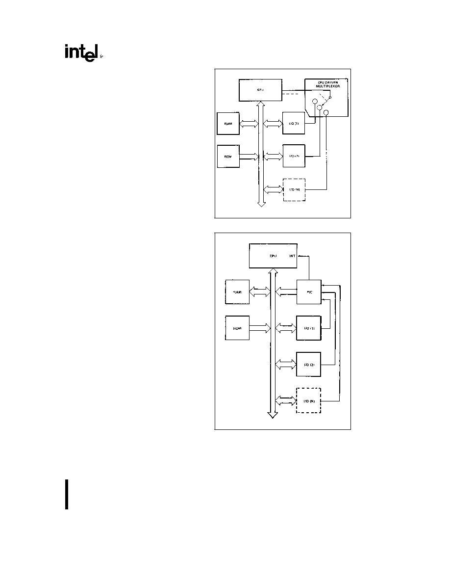
Figure 3a Polled Method
231468 ≠ 4
Figure 3b Interrupt Method
3

8259A
The 8259A is a device specifically designed for use
in real time interrupt driven microcomputer systems
It manages eight levels or requests and has built-in
features for expandability to other 8259A's (up to 64
levels) It is programmed by the system's software
as an I O peripheral A selection of priority modes is
available to the programmer so that the manner in
which the requests are processed by the 8259A can
be configured to match his system requirements
The priority modes can be changed or reconfigured
dynamically at any time during the main program
This means that the complete interrupt structure can
be defined as required based on the total system
environment
INTERRUPT REQUEST REGISTER (IRR) AND
IN-SERVICE REGISTER (ISR)
The interrupts at the IR input lines are handled by
two registers in cascade the Interrupt Request Reg-
ister (IRR) and the In-Service (ISR) The IRR is used
to store all the interrupt levels which are requesting
service and the ISR is used to store all the interrupt
levels which are being serviced
PRIORITY RESOLVER
This logic block determines the priorites of the bits
set in the IRR The highest priority is selected and
strobed into the corresponding bit of the ISR during
INTA pulse
INTERRUPT MASK REGISTER (IMR)
The IMR stores the bits which mask the interrupt
lines to be masked The IMR operates on the IRR
Masking of a higher priority input will not affect the
interrupt request lines of lower quality
INT (INTERRUPT)
This output goes directly to the CPU interrupt input
The V
OH
level on this line is designed to be fully
compatible with the 8080A 8085A and 8086 input
levels
INTA (INTERRUPT ACKNOWLEDGE)
INTA pulses will cause the 8259A to release vector-
ing information onto the data bus The format of this
data depends on the system mode (mPM) of the
8259A
DATA BUS BUFFER
This 3-state bidirectional 8-bit buffer is used to inter-
face the 8259A to the system Data Bus Control
words
and
status
information
are
transferred
through the Data Bus Buffer
READ WRITE CONTROL LOGIC
The function of this block is to accept OUTput com-
mands from the CPU It contains the Initialization
Command Word (ICW) registers and Operation
Command Word (OCW) registers which store the
various control formats for device operation This
function block also allows the status of the 8259A to
be transferred onto the Data Bus
CS (CHIP SELECT)
A LOW on this input enables the 8259A No reading
or writing of the chip will occur unless the device is
selected
WR (WRITE)
A LOW on this input enables the CPU to write con-
trol words (ICWs and OCWs) to the 8259A
RD (READ)
A LOW on this input enables the 8259A to send the
status of the Interrupt Request Register (IRR) In
Service Register (ISR) the Interrupt Mask Register
(IMR) or the Interrupt level onto the Data Bus
A
0
This input signal is used in conjunction with WR and
RD signals to write commands into the various com-
mand registers as well as reading the various status
registers of the chip This line can be tied directly to
one of the address lines
4

8259A
231468 ≠ 5
Figure 4a 8259A Block Diagram
5