 | –≠–ª–µ–∫—Ç—Ä–æ–Ω–Ω—ã–π –∫–æ–º–ø–æ–Ω–µ–Ω—Ç: 82801E | –°–∫–∞—á–∞—Ç—å:  PDF PDF  ZIP ZIP |

Intel
Æ
82801E Communications I/O
Controller Hub (C-ICH)
for Applied Computing
Advance Information Datasheet
Product Features
s
Supports Intel processors, the
82815E GMCH and the 82810E GMCH
s
8-Bit Hub Interface
-- 266 Mbyte/s maximum throughput
s
Two integrated LAN controllers
s
USB
-- Includes one UHCI Host Controller
with a total of two ports
-- USB 1.1 compliant
s
PCI Bus interface
-- Supports PCI Rev 2.2 specification at
33 MHz
-- 133 Mbyte/s maximum throughput
s
Low-Pincount (LPC) interface
s
Firmware Hub (FWH) interface
-- Supports 8-Mbyte memory size
s
Integrated IDE controller supports
Ultra100 DMA, Ultra66 and Ultra33
DMA mode transfers
s
Interrupt Controller
-- Two cascaded 82C59 interrupt
controllers
-- Integrated I/O (x) APIC supporting 24
interrupts
-- 15 interrupts supported in 8259 mode
s
Two cascaded 8237 DMA controllers
s
Integrated 82C54-compatible timers
s
Real-time clock with 256-byte battery-
backed CMOS RAM
s
System Management Bus (SMBus)
-- Compatible with most two-wire
components that are also I
2
C compatible
-- Slave interface allows external
microcontroller to access system
resources
s
GPIO
-- Exact number varies by configuration.
Maximum: 12 inputs, eight outputs, four
I/O
s
Integrated 16550 compatible UARTs
-- Two UARTs
-- Serial Interrupts
s
Supports IRQ1/IRQ12 emulation to avoid
external keyboard controller
s
1.8 V operation with 3.3 V I/O. 5 V
tolerance on many buffers, including PCI
and IDE
s
Package: 421 BGA
Order Number: 273598-003
January 2002
Notice: This document contains information on products in the sampling and initial production
phases of development. The specifications are subject to change without notice. Verify with your
local Intel sales office that you have the latest datasheet before finalizing a design.

2
Advance Information Datasheet
Information in this document is provided in connection with Intel
Æ
products. No license, express or implied, by estoppel or otherwise, to any intellectual
property rights is granted by this document. Except as provided in Intel's Terms and Conditions of Sale for such products, Intel assumes no liability
whatsoever, and Intel disclaims any express or implied warranty, relating to sale and/or use of Intel products including liability or warranties relating to
fitness for a particular purpose, merchantability, or infringement of any patent, copyright or other intellectual property right. Intel products are not
intended for use in medical, life saving, or life sustaining applications.
Intel may make changes to specifications and product descriptions at any time, without notice.
Designers must not rely on the absence or characteristics of any features or instructions marked "reserved" or "undefined." Intel reserves these for
future definition and shall have no responsibility whatsoever for conflicts or incompatibilities arising from future changes to them.
The Intel
Æ
82801E Communications I/O Controller Hub may contain design defects or errors known as errata which may cause the product to deviate
from published specifications. Current characterized errata are available on request.
Contact your local Intel sales office or your distributor to obtain the latest specifications and before placing your product order.
Copies of documents which have an ordering number and are referenced in this document, or other Intel literature may be obtained by calling
1-800-548-4725 or by visiting Intel's website at http://www.intel.com.
Copyright © Intel Corporation, 2002
AlertVIEW, i960, AnyPoint, AppChoice, BoardWatch, BunnyPeople, CablePort, Celeron, Chips, Commerce Cart, CT Connect, CT Media, Dialogic,
DM3, EtherExpress, ETOX, FlashFile, GatherRound, i386, i486, iCat, iCOMP, Insight960, InstantIP, Intel, Intel logo, Intel386, Intel486, Intel740,
IntelDX2, IntelDX4, IntelSX2, Intel ChatPad, Intel Create&Share, Intel Dot.Station, Intel GigaBlade, Intel InBusiness, Intel Inside, Intel Inside logo, Intel
NetBurst, Intel NetStructure, Intel Play, Intel Play logo, Intel Pocket Concert, Intel SingleDriver, Intel SpeedStep, Intel StrataFlash, Intel TeamStation,
Intel WebOutfitter, Intel Xeon, Intel XScale, Itanium, JobAnalyst, LANDesk, LanRover, MCS, MMX, MMX logo, NetPort, NetportExpress, Optimizer
logo, OverDrive, Paragon, PC Dads, PC Parents, Pentium, Pentium II Xeon, Pentium III Xeon, Performance at Your Command, ProShare,
RemoteExpress, Screamline, Shiva, SmartDie, Solutions960, Sound Mark, StorageExpress, The Computer Inside, The Journey Inside, This Way In,
TokenExpress, Trillium, Vivonic, and VTune are trademarks or registered trademarks of Intel Corporation or its subsidiaries in the United States and
other countries.
*Other names and brands may be claimed as the property of others.

Advance Information Datasheet
3
Contents
Contents
1.0
Introduction....................................................................................................................................7
1.1
Overview ............................................................................................................................... 9
1.2
About this Document .......................................................................................................... 10
2.0
Package Information ................................................................................................................... 11
2.1
Ball Location ....................................................................................................................... 11
2.2
Mechanical Specifications .................................................................................................. 23
3.0
Signal Descriptions ..................................................................................................................... 25
3.1
Alphabetical Signal Reference............................................................................................25
3.2
Signals Grouped By Type ................................................................................................... 36
3.2.1
Hub Interface to Host Controller ............................................................................ 36
3.2.2
Link to LAN Connect .............................................................................................. 36
3.2.3
EEPROM Interface ................................................................................................ 36
3.2.4
Firmware Hub Interface ......................................................................................... 37
3.2.5
PCI Interface .......................................................................................................... 37
3.2.6
IDE Interface .......................................................................................................... 40
3.2.7
LPC Interface ......................................................................................................... 41
3.2.8
Interrupt Interface .................................................................................................. 41
3.2.9
USB Interface ........................................................................................................42
3.2.10 Power Signals ........................................................................................................42
3.2.11 Processor Interface................................................................................................ 43
3.2.12 SMBus Interface .................................................................................................... 44
3.2.13 System Management Interface ..............................................................................44
3.2.14 Real Time Clock Interface .....................................................................................44
3.2.15 Other Clocks .......................................................................................................... 45
3.2.16 Universal Asynchronous Receive and Transmit (UART 0,1) .................................45
3.2.17 SIU LPC Interface .................................................................................................. 46
3.2.18 Miscellaneous Signals ........................................................................................... 47
3.2.19 General Purpose I/O .............................................................................................. 47
3.2.20 Power and Ground.................................................................................................48
3.3
Pin Straps ...........................................................................................................................49
3.3.1
Functional Straps ................................................................................................... 49
3.3.2
Test Signals ........................................................................................................... 49
3.3.2.1
Test Mode Selection ..............................................................................49
3.3.2.2
Test Straps............................................................................................. 50
3.3.3
External RTC Circuitry ........................................................................................... 50
3.3.4
V5REF/Vcc3_3 Sequencing Requirements ...........................................................51
3.4
Power Planes and Pin States ............................................................................................. 51
3.4.1
Power Planes......................................................................................................... 51
3.4.2
Integrated Pull-Ups and Pull-Downs ...................................................................... 52
3.4.3
IDE Integrated Series Termination Resistors......................................................... 52
3.4.4
Output and I/O Signals Planes and States ............................................................ 53
3.4.5
Power Planes for Input Signals..............................................................................55
4.0
Electrical Characteristics............................................................................................................ 57
4.1
Absolute Maximum Ratings ................................................................................................ 57

Contents
4
Advance Information Datasheet
4.2
Functional Operating Range............................................................................................... 57
4.3
DC Characteristics.............................................................................................................. 58
4.4
AC Characteristics .............................................................................................................. 62
4.5
Timing Diagrams................................................................................................................. 70
5.0
Testability..................................................................................................................................... 77
5.1
Test Mode Description........................................................................................................ 77
5.2
Tri-state Mode..................................................................................................................... 78
5.3
XOR Chain Mode................................................................................................................ 78
5.3.1
XOR Chain Testability Algorithm Example ............................................................ 84
5.3.1.1
Test Pattern Consideration for XOR Chain 4......................................... 84
Figures
1
System Configuration ................................................................................................................... 7
2
Intel
Æ
82801E C-ICH Simplified Block Diagram ........................................................................... 8
3
Ball Diagram (Top View)............................................................................................................. 11
4
Intel
Æ
82801E C-ICH Package (Top View) ................................................................................. 23
5
Intel
Æ
82801E C-ICH Package (Side View) ................................................................................ 24
6
Intel
Æ
82801E C-ICH Package (Bottom View)............................................................................ 24
7
Required External RTC Circuit ................................................................................................... 50
8
Example V5REF Sequencing Circuit .......................................................................................... 51
9
Clock Timing ............................................................................................................................... 70
10
Valid Delay From Rising Clock Edge.......................................................................................... 70
11
Setup And Hold Times................................................................................................................ 71
12
Float Delay ................................................................................................................................. 71
13
Pulse Width ................................................................................................................................ 71
14
Output Enable Delay .................................................................................................................. 71
15
IDE PIO Mode ............................................................................................................................ 72
16
IDE Multiword DMA .................................................................................................................... 72
17
Ultra ATA Mode (Drive Initiating a Burst Read) .......................................................................... 73
18
Ultra ATA Mode (Sustained Burst) ............................................................................................. 73
19
Ultra ATA Mode (Pausing a DMA Burst) .................................................................................... 74
20
Ultra ATA Mode (Terminating a DMA Burst) .............................................................................. 74
21
USB Rise and Fall Times ........................................................................................................... 74
22
USB Jitter ................................................................................................................................... 75
23
USB EOP Width ......................................................................................................................... 75
24
SMBus Transaction .................................................................................................................... 75
25
SMBus Time-out ......................................................................................................................... 75
26
Power Sequencing and Reset Signal Timings ........................................................................... 76
27
1.8 V/3.3 V Power Sequencing................................................................................................... 76
28
C0 to C2 to C0 Timings .............................................................................................................. 76
29
Test Mode Entry (XOR Chain Example)..................................................................................... 77
30
Example XOR Chain Circuitry .................................................................................................... 78

Advance Information Datasheet
5
Contents
Tables
1
PCI Devices and Functions ..........................................................................................................9
2
Related Documents ....................................................................................................................10
3
Industry Specifications................................................................................................................ 10
4
Ball List By Number ....................................................................................................................12
5
Ball List By Signal Name ............................................................................................................ 17
6
82801E C-ICH Signal Description .............................................................................................. 25
7
Hub Interface Signals ................................................................................................................. 36
8
LAN Interface.............................................................................................................................. 36
9
EEPROM Interface ..................................................................................................................... 36
10
Firmware Hub Interface Signals .................................................................................................37
11
PCI Interface Signals .................................................................................................................. 37
12
IDE Interface Signals .................................................................................................................. 40
13
LPC Interface Signals ................................................................................................................. 41
14
Interrupt Signals.......................................................................................................................... 41
15
USB Interface Signals................................................................................................................. 42
16
Power Signals............................................................................................................................. 42
17
Processor Interface Signals ........................................................................................................43
18
SMBus Interface Signals ............................................................................................................ 44
19
System Management Interface Signals ...................................................................................... 44
20
Real Time Clock Interface .......................................................................................................... 44
21
Other Clocks ............................................................................................................................... 45
22
Universal Asynchronous Receive And Transmit (UART 0, 1) ....................................................45
23
SIU Interface............................................................................................................................... 46
24
Miscellaneous Signals ................................................................................................................ 47
25
General Purpose I/O Signals ...................................................................................................... 47
26
Power and Ground Signals......................................................................................................... 48
27
Functional Strap Definitions ........................................................................................................49
28
Test Mode Selection ................................................................................................................... 49
29
82801E C-ICH Power Planes ..................................................................................................... 51
30
Integrated Pull-Up and Pull-Down Resistors ..............................................................................52
31
IDE Series Termination Resistors............................................................................................... 52
32
Power Plane and States for Output and I/O Signals................................................................... 53
33
Power Plane for Input Signals ................................................................................................ .... 56
34
Absolute Maximum Ratings ........................................................................................................57
35
Functional Operating Range....................................................................................................... 57
36
82801E C-ICH Power Consumption Measurements ..................................................................58
37
DC Characteristic Input Signal Association ................................................................................ 58
38
DC Input Characteristics............................................................................................................. 59
39
DC Characteristic Output Signal Association ............................................................................. 59
40
DC Output Characteristics .......................................................................................................... 60
41
Other DC Characteristics............................................................................................................ 61
42
Clock Timings ............................................................................................................................. 62
43
Clock Timings - UART_CLK ....................................................................................................... 63
44
PCI Interface Timing ................................................................................................................... 63
45
IDE PIO & Multiword DMA Mode Timing .................................................................................... 64
46
Ultra ATA Timing (Mode 0, Mode 1, Mode 2) ............................................................................. 65
47
Ultra ATA Timing (Mode 3, Mode 4, Mode 5) ............................................................................. 66
48
Universal Serial Bus Timing........................................................................................................67
49
IOAPIC Bus Timing..................................................................................................................... 68
Contents
6
Advance Information Datasheet
50
SMBus Timing ............................................................................................................................ 68
51
SIU LPC and Serial IRQ Timings ............................................................................................... 68
52
UART Timings ............................................................................................................................ 69
53
LPC Timing ................................................................................................................................. 69
54
Miscellaneous Timings ............................................................................................................... 69
55
Power Sequencing and Reset Signal Timings ........................................................................... 70
56
Test Mode Selection ................................................................................................................... 77
57
XOR Chain #1 ............................................................................................................................ 79
58
XOR Chain #2; Chain 2-1 and Chain 2-2 ................................................................................... 80
59
XOR Chain #3; Chain 3-1 and Chain 3-2 ................................................................................... 81
60
XOR Chain #4; Chain 4-1 and Chain 4-2 ................................................................................... 82
61
Signals Not in XOR Chain .......................................................................................................... 83
62
XOR Test Pattern Example ........................................................................................................ 84
Revision History
Date
Revision
Description
January 2001
003
Corrected XOR Chain 2. Added note to CPUSLP# signal
description.
December 2001
002
Corrected pinouts and pin list.
December 2001
001
First release of this datasheet.

Intel
Æ
82801E C-ICH
Advance Information Datasheet
7
1.0
Introduction
The Intel
Æ
82801E Communications I/O Controller Hub (82801E C-ICH) is a highly integrated
multifunctional communications I/O controller hub that provides the interface to the PCI bus and
integrates many of the functions needed in today's communications applications. This document
provides a detailed description of the 82801E C-ICH thermal, electrical and mechanical
specifications, including signals, pinout, packaging, electrical characteristics, and testability.
Figure 1 illustrates the typical system configuration using the 82801E C-ICH. Figure 2 is a
simplified block diagram of the functional units of the 82801E C-ICH.
Figure 1. System Configuration
Main
Memory
Processor
sys_blk_CICH.vsd
PCI Bus
Up to Four
PCI Slots
Host
Controller
Communications
I/O Controller Hub
(C-ICH)
FWH
Two USB Ports
GPIO
LPC I/F
Graphics
Controller
SMBus
Device(s)
SMBus
ATA/100/66/33
4 IDE Drives
Hub Interface
Two LAN Controllers
Two UARTs

Intel
Æ
82801E C-ICH
8
Advance Information Datasheet
Figure 2. Intel
Æ
82801E C-ICH Simplified Block Diagram
INTRUDER#
SMLINK[1:0]
HL[11:0]
HL_STB
HL_STB#
HLCOMP
PWROK
RSMRST#
RSM_PWROK
VRMPWRGD
AD[31:0]
C/BE[3:0]#
DEVSEL#
FRAME#
IRDY#
TRDY#
STOP#
PAR
PERR#
REQ[3:0]#
REQ[5]#/REQ[B]#/GPIO[1]
REQ[A]#/GPIO[0]
GNT[3:0]#
GNT[5]#/GNT[B]#/GPIO[17]
GNT[A]#/GPIO[16]
PCICLK
PCIRST#
PLOCK#
SERR#
Interrupt
A20M#
CPUSLP#
FERR#
IGNNE#
INIT#
INTR
NMI
SMI#
STPCLK#
RCIN#
A20GATE
CPUPWRGD
Processor
Interface
PCI
Interface
USB
SERIRQ
PIRQ[A:F]#
PIRQ[G:H]/GPIO[5:4]
IRQ[15:14]
APICCLK
APICD[1:0]
USBP1P
USBP1N
USBP0P
USBP0N
OC[1:0]#
RTCX1
RTCX2
CLK14
CLK48
CLK66
RTC
Clocks
Miscellaneous
Signals
SPKR
RTCRST#
TP[3:0]
PDCS1#
SDCS1#
PDCS3#
SDCS3#
PDA[2:0]
SDA[2:0]
PDD[15:0]
SDD[15:0]
PDDREQ
SDDREQ
PDDACK#
SDDACK#
PDIOR#
SDIOR#
PDIOW#
SDIOW#
PIORDY
SIORDY
IDE
Interface
Hub
Interface
LPC
Interface
SMBus
Interface
Power
Signals
Firmware
Hub
System
Manage-
ment
General
Purpose
I/O
FWH[3:0]/LAD[3:0]
FWH[4]/LFRAME#
LAD[3:0]/FWH[3:0]
LFRAME#/FWH[4]
LDRQ[1:0]#
SMBDATA
SMBCLK
SMBALERT#/GPIO[11]
GPIO[13:11,8:4,1:0]
GPIO[23:16]
GPIO[28:27,25:24]
LAN1_CLK
LAN1_RXD[2:0]
LAN1_TXD[2:0]
LAN1_RSTSYNC
LAN1
EEPROM1
EE1_SHCLK
EE1_DIN
EE1_DOUT
EE1_CS
LAN0_CLK
LAN0_RXD[2:0]
LAN0_TXD[2:0]
LAN0_RSTSYNC
LAN0
Serial I/O
Unit
SIU_LCLK
SIU0_RXD
SIU0_TXD
SIU0_CTS#
SIU0_DSR#
SIU0_DCD#
SIU0_RI#
SIU0_DTR#
SIU0_RTS#
SIU_RESET#
SIU_LAD[3:0]
EE0_SHCLK
EE0_DIN
EE0_DOUT
EE0_CS
EEPROM0
UART_CLK
SIU1_RXD
SIU1_TXD
SIU1_CTS#
SIU1_DSR#
SIU1_DCD#
SIU1_RI#
SIU1_DTR#
SIU1_RTS#
SIU_LFRAME#
SIU_LDRQ#
SIU_SERIRQ
Blk_CICH.vsd
THRM#
RI#
SUSCLK
Intel
Æ
82801E C-ICH
Advance Information Datasheet
9
1.1
Overview
The 82801E C-ICH provides extensive I/O support. Functions and capabilities include:
∑
PCI Rev 2.2 compliant with support for 33 MHz PCI operations
∑
PCI slots support up to four Req/Gnt pairs
∑
Enhanced DMA Controller, Interrupt Controller, and Timer Functions
∑
Integrated IDE controller supports Ultra ATA100/66/33
∑
USB host interface with support for two USB ports; one host controller
∑
Two integrated LAN controllers
∑
System Management Bus (SMBus) with additional support for I
2
C devices
∑
Low Pin Count (LPC) interface
∑
Firmware Hub (FWH) interface support
∑
Serial I/O unit containing two UARTs
The 82801E C-ICH incorporates a variety of PCI functions that are divided into two logical
devices (30 and 31) on PCI Bus 0 and one device on Bus 1. Device 30 is the Hub Interface-to-PCI
bridge. Device 31 contains all the other PCI functions, except the LAN controller as shown in
Table 1. The LAN controllers are located on Bus 1.
Table 1. PCI Devices and Functions
Bus:Device:Function
Function Description
Bus 0:Device 30:Function 0
Hub Interface to PCI Bridge
Bus 0:Device 31:Function 0
PCI to LPC Bridge
(includes: DMA, Timers, compatible interrupt controller, APIC, RTC, SIU,
processor interface control, power management control, system
management control, and GPIO control)
Bus 0:Device 31:Function 1
IDE Controller
Bus 0:Device 31:Function 2
USB Controller
Bus 0:Device 31:Function 3
SMBus Controller
Bus 1:Device 8:Function 0
LAN0 Controller
Bus 1:Device 9:Function 0
LAN1 Controller

Intel
Æ
82801E C-ICH
10
Advance Information Datasheet
1.2
About this Document
This document is intended for original equipment manufacturers (OEMs) and BIOS vendors
creating 82801E C-ICH-based products. This document contains electrical thermal and mechanical
specifications for the 82801E C-ICH, including complete signal descriptions, pin maps, and
testability information. For additional information, refer to the documents listed in Table 2.
This document assumes a working knowledge of the vocabulary and principles of USB, IDE,
SMBus, PCI, LAN, LPC, and serial I/O. Details of these features are described in the Intel
Æ
82801E Communications I/O Controller Hub (C-ICH) Developer's Manual (order number 273599)
and in the industry specifications listed in Table 3.
Table
2. Related
Documents
Document
Order Number
Intel
Æ
82801E Communications I/O Controller Hub (C-ICH) Developer's Manual
273599
Intel
Æ
82801E Communications I/O Controller Hub (C-ICH) Specification Update
273645
Intel
Æ
82801E Communications I/O Controller Hub (C-ICH) Platform Design Guide
273671
Intel
Æ
810E Chipset: 82810E Graphics and Memory Controller Hub (GMCH)
Datasheet
290676
82802AB/82802AC Firmware Hub (FWH)
Datasheet
290658
Table 3. Industry Specifications
Specification
Location
LPC
http://developer.intel.com/design/chipsets/industry/lpc.htm
WfM
http://developer.intel.com/ial/WfM/usesite.htm
SMBus
http://www.sbs-forum.org/specs/
PCI
http://pcisig.com/
USB
http://www.usb.org

Intel
Æ
82801E C-ICH
Advance Information Datasheet
11
2.0
Package Information
2.1
Ball Location
This section describes the 82801E C-ICH ball assignment. Figure 3 provides a 421-ball location
diagram. The diagram also indicates general signal groupings. Table 4 lists the 82801E C-ICH
signal assignments by ball number. Table 5 lists the assignments alphabetically by signal name.
Figure 3. Ball Diagram (Top View)
A8684-02
IDE
SMLINK
POWER
MANAGEMENT
SIU
LPC
PCI
LAN
PCI
SMBUS
USB
HUB INTERFACE
PROCESSOR
IDE
A
C
B
E
D
G
F
J
H
L
K
N
M
R
P
U
T
W
V
AA
Y
AC
AB
A
C
B
E
D
G
F
J
H
L
K
N
M
R
P
U
T
W
V
AA
Y
AC
AB
23
22
21
20
19
18
17
16
15
14
13
12
11
10
9
8
7
6
5
4
3
2
1
23
22
21
20
19
18
17
16
15
14
13
12
11
10
9
8
7
6
5
4
3
2
1
PIRQ[A]# VSS
NC[4]
GNT[3]#
VSS
AD[28]
VSS
SIU0_
RI#
UART_
CLK
VSS
SIU_
LAD[1]
LAN1_
TXD[1]
VSS
SIU1_
DSR#
SIU1_
RTS#
SIU_
SERIRQ
TP[0]
VSS
THRM#
GPIO[21]
VSS
GNT[0]#
PIRQ[H]#/
GPIO[5]
REQ[0]# NC[5]
AD[26]
AD[22]
FRAME# AD[16]
LAN1_
RXD[2]
LAN1_
CLK
SIU0_
DTR#
VCC3_3
SIU_
LFRAME#
Vcc1_8
SIU0_
DCD#
SIU1_
RXD
SIU1_
DTR#
Vcc1_8
LAD[0]/
FWH[0]
LAD[3]/
FWH[3]
LDRQ[0]#
GNT[A]#/
GPIO[16]
GNT[B]#/
GNT[5]#/
GPIO[17]
VCC1_8
PIRQ[D]#
AD[30]
VSS
VSS
PAR
AD[13]
AD[20]
EE0_
SHCLK
LAN1_
RXD[0]
VSS
SIU1_
TXD
SIU_
LDRQ#
LAN1_
RSTSYNC
LAN1_
TXD[0]
Vcc3_3
SIU1_
DCD#
SIU_
LAD[2]
VSS LFRAME#/
FWH[4]
LDRQ[1]#
REQ[B]#/
REQ[5]#/
GPIO[1]
REQ[A]#/
GPIO[0]
PIRQ[E]#
PIRQ[C]#
AD[18] AD[24]
STOP#
AD[15]
VSS
AD[4]
LAN0_
RSTSYNC
EE1_
DOUT
SIU0_
TXD
SIU0_
CTS#
SIU1_
RI#
VSS
LAN1_
TXD[2]
SIU0_
DSR#
SIU1_
CTS#
SIU_
LAD[0]
LAD[1]/
FWH[1]
SIU_
RESET#
V5REF
GNT[1]#
VSS
PIRQ[B]#
REQ[1]#
VSS
Vcc3_3
TRDY#
AD[9]
AD[0]
Vcc1_8
LAN0_
TXD[2]
EE0_
DIN
VSS
SIU0_
RXD
VSS
LAN0_
RXD[2]
EE1_
SHCLK
Vcc3_3
SIU0_
RTS#
SIU_
LAD[3]
LAD[2]/
FWH[2]
SIU_
LCLK
PIRQ[G]#/
GPIO[4]
PIRQ[F]#
REQ[2]#
GNT[2]#
VSS
V5REF Vcc3_3
NC[6]
Vcc3_3
NC[10]
USBP1N
IGNNE#
V_CPU_IO
SDDACK#
Vcc3_3
Vcc3_3
CPUPWRGD
SIORDY
Vcc3_3
Vcc3_3
Vcc3_3
Vcc3_3
Vcc3_3
Vcc3_3
Vcc3_3
VSS
VSS
OC[1]#
NC[7]
USBP1P
NC[9]
RCIN#
VRMPWRGD
SDIOW#
SDD[14]
PDA[1]
V_CPU_IO
SDA[2]
SDIOR#
SDD[5]
PDD[1]
CLK14
PDD[5]
PDCS1#
Vcc3_3
PWROK
VccRTC
NC[1]
SMLINK[0] VSS
RESERVED2
V5REF
VSS
NC[8]
A20GATE
SDCS3#
SDD[0]
SDD[10]
SDD[6]
GPIO[18]
SDD[15]
SDD[12]
PDA[0]
PDD[12]
PDD[6]
PDD[10]
PDIOW#
APICD[1]
NC[2]
RSMRST#
RTCX1
TP[1]
RTCRST#
SMLINK[1]
VSS
OC0#
VSS
GPIO[19]
SDA[1]
SDD[3]
SDD[8]
PDDACK#
VSS
VSS
SDD[4]
VSS
PDD[3]
PDD[7]
VSS
PDD[0]
SERIRQ
FERR#
VccRTC
RTCX2
INTRUDER#
VBIAS
GPIO[24]
Vcc3_3
V5REF
TP[3]
SDA[0]
Vcc3_3
SDD[11]
PDIOR#
PDD[15]
IRQ[15]
SDD[13]
SDD[9]
IRQ[14]
PDD[13]
PDD[8]
PDD[4]
PDD[14]
SPKR
APICD[0]
CLK48
VSS
VSS
VSS
VSS
VSS
VSS
TP[2]
VSS
SDD[1]
PDCS3#
PIORDY
PDDREQ
SDDREQ
SDD[2]
SDD[7]
PDA[2]
VSS
PDD[9]
PDD[11]
PDD[2]
V5REF
APICCLK
VSS
NC[3]
Vcc3_3
C/BE[2]#
VSS
VSS
Vcc1_8
PLOCK# Vcc3_3
Vcc3_3
IRDY#
AD[17]
AD[19]
AD[23]
VSS
VSS
HLCOMP
HL[11]
HUBREF
Vcc1_8
Vcc1_8
Vcc1_8
Vcc1_8
VSS
VSS
VSS
Vcc1_8
AD[21]
C/BE[3]#
VSS
AD[27]
AD[25]
HL[2]
HL[1]
HL[0]
VSS
VSS
Vcc1_8
VSS
VSS
VSS
VSS
Vcc1_8
GPIO[28]
GPIO[27]
VSS
GPIO[7]
HL_STB#
HL[10]
HL[4]
VSS
VSS
VSS
VSS
VSS
VSS
VSS
VSS
RESERVED1
GPIO[13]
GPIO[8]
GPIO[12]
VSS
VSS
HL[7]
HL[8]
HL[5]
Vcc1_8
Vcc1_8
VSS
Vcc1_8
Vcc3_3
Vcc1_8
RI#
SMBDATA
Vcc3_3
PCIRST#
GPIO[25]
HL[6]
VSS
CPUSLP#
VSS
VSS
Vcc3_3
Vcc1_8
USBP0N
NC[12]
RSM_PWROK
VSS
SMBCLK
A20M#
SMI#
GPIO[20]
STPCLK#
GPIO[23]
Vcc3_3
Vcc3_3
VSS
USBP0P
SUSCLK
SMBALERT#/
GPIO[11]
NC[11]
INTR
INIT#
SDCS1#
NMI
GPIO[22]
VSS
PCICLK
REQ[3]#
GPIO[6]
AD[29]
AD[31]
VSS
VSS
HL[9]
HL_STB
HL[3]
Vcc1_8
VSS
VSS
Vcc1_8
AD[11] Vcc3_3
C/BE[0]#
AD[6]
AD[7]
AD[10]
Vcc1_8
Vcc1_8
EE1_CS
Vcc3_3
Vcc3_3
LAN0_CLK
EE0_CS
Vcc3_3
AD[2]
Vcc3_3
AD[3]
VSS
SERR#
AD[12]
LAN0_
RXD[1]
LAN0_
TXD[1]
EE1_
DIN
VSS
EE0_
DOUT
Vcc3_3
AD[5]
Vcc3_3
AD[1]
AD[8]
C/BE[1]# AD[14]
VSS
LAN0_
TXD[0]
LAN1_
RXD[1]
Vcc1_8
LAN0_
RXD[0]
Vcc3_3
VSS
PERR#
DEVSEL#
VSS
CLK66
(HLCLK)
VSS
VSS
VSS
Vcc3_3
Vcc1_8
Vcc1_8
Vcc1_8
Vcc1_8
Vcc3_3
Intel
Æ
82801E C-ICH
12
Advance Information Datasheet
Table 4. Ball List By Number
Ball Number
Signal Name
A1
VSS
A2
AD[28]
A3
GNT[3]#
A4
NC[4]
A5
PIRQ[A]#
A6
VSS
A7
PIRQ[H]#/GPIO[5]
A8
GNT[0]#
A9
VSS
A10
GPIO[21]
A11
THRM#
A12
TP[0]
A13
VSS
A14
SIU_SERIRQ
A15
SIU_LAD[1]
A16
SIU1_RTS#
A17
VSS
A18
SIU1_DSR#
A19
UART_CLK
A20
VSS
A21
SIU0_RI#
A22
LAN1_TXD[1]
A23
VSS
B1
FRAME#
B2
AD[16]
B3
AD[22]
B4
AD[26]
B5
REQ[0]#
B6
NC[5]
B7
PIRQ[D]#
B8
Vcc1_8
B9
GNT[B]#/GNT[5]#/GPIO[17]
B10
GNT[A]#/GPIO[16]
B11
LDRQ[0]#
B12
LAD[0]/FWH[0]
B13
LAD[3]/FWH[3]
B14
Vcc1_8
B15
SIU_LFRAME#
B16
SIU1_DTR#
B17
Vcc3_3
B18
SIU1_RXD
B19
SIU0_DTR#
B20
SIU0_DCD#
B21
LAN1_CLK
B22
Vcc1_8
B23
LAN1_RXD[2]
C1
AD[13]
C2
AD[20]
C3
PAR
C4
VSS
C5
AD[30]
C6
VSS
C7
PIRQ[C]#
C8
PIRQ[E]#
C9
REQ[A]#/GPIO[0]
C10
REQ[B]#/REQ[5]#/GPIO[1]
C11
LDRQ[1]#
C12
VSS
C13
LFRAME#/FWH[4]
C14
SIU_LAD[2]
C15
SIU_LDRQ#
C16
SIU1_DCD#
C17
SIU1_TXD
C18
Vcc3_3
C19
VSS
C20
LAN1_TXD[0]
C21
LAN1_RXD[0]
C22
LAN1_RSTSYNC
C23
EE0_SHCLK
D1
VSS
D2
AD[4]
D3
AD[15]
D4
STOP#
D5
AD[18]
D6
AD[24]
D7
REQ[1]#
D8
PIRQ[B]#
D9
VSS
D10
GNT[1]#
D11
V5REF
D12
LAD[1]/FWH[1]
D13
SIU_RESET#
D14
SIU_LAD[0]
D15
SIU1_RI#
D16
SIU1_CTS#
D17
SIU0_CTS#
D18
SIU0_DSR#
Table 4. Ball List By Number
Ball Number
Signal Name
Intel
Æ
82801E C-ICH
Advance Information Datasheet
13
D19
SIU0_TXD
D20
LAN1_TXD[2]
D21
EE1_DOUT
D22
VSS
D23
LAN0_RSTSYNC
E1
AD[0]
E2
Vcc1_8
E3
AD[9]
E4
TRDY#
E5
VSS
E6
Vcc3_3
E7
VSS
E8
GNT[2]#
E9
REQ[2]#
E10
PIRQ[F]#
E11
PIRQ[G]#/GPIO[4]
E12
LAD[2]/FWH[2]
E13
SIU_LCLK
E14
SIU_LAD[3]
E15
VSS
E16
SIU0_RTS#
E17
SIU0_RXD
E18
Vcc3_3
E19
VSS
E20
EE1_SHCLK
E21
EE0_DIN
E22
LAN0_RXD[2]
E23
LAN0_TXD[2]
F1
AD[7]
F2
AD[10]
F3
AD[6]
F4
C/BE[0]#
F5
AD[11]
F6
Vcc3_3
F7
Vcc3_3
F8
Vcc1_8
F9
Vcc1_8
F10
Vcc1_8
F14
Vcc1_8
F15
Vcc3_3
F16
Vcc3_3
F17
Vcc3_3
F18
Vcc3_3
F19
EE1_CS
Table 4. Ball List By Number
Ball Number
Signal Name
F20
EE0_CS
F21
Vcc1_8
F22
LAN0_CLK
F23
Vcc1_8
G1
SERR#
G2
AD[12]
G3
VSS
G4
AD[3]
G5
AD[2]
G6
Vcc3_3
G18
Vcc3_3
G19
EE1_DIN
G20
EE0_DOUT
G21
LAN0_TXD[1]
G22
VSS
G23
LAN0_RXD[1]
H1
C/BE[1]#
H2
AD[14]
H3
AD[8]
H4
AD[1]
H5
AD[5]
H6
Vcc3_3
H18
Vcc3_3
H19
LAN1_RXD[1]
H20
LAN0_RXD[0]
H21
LAN0_TXD[0]
H22
Vcc1_8
H23
VSS
J1
VSS
J2
C/BE[2]#
J3
DEVSEL#
J4
PERR#
J5
VSS
J6
Vcc3_3
J18
Vcc1_8
J19
VSS
J20
VSS
J21
VSS
J22
VSS
J23
CLK66 (HLCLK)
K1
AD[23]
K2
AD[19]
K3
AD[17]
K4
IRDY#
Table 4. Ball List By Number
Ball Number
Signal Name

Intel
Æ
82801E C-ICH
14
Advance Information Datasheet
K5
PLOCK#
K6
Vcc3_3
K10
Vcc1_8
K11
VSS
K12
Vcc1_8
K13
VSS
K14
Vcc1_8
K18
Vcc1_8
K19
HLCOMP
K20
HUBREF
K21
VSS
K22
HL[11]
K23
VSS
L1
AD[27]
L2
AD[25]
L3
VSS
L4
C/BE[3]#
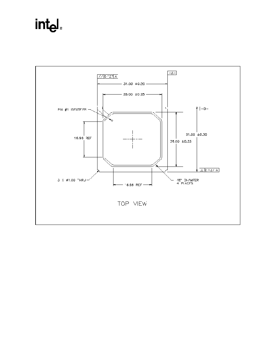
L5
AD[21]
L10
VSS
L11
VSS
L12
VSS
L13
VSS
L14
Vcc1_8
L19
HL[0]
L20
VSS
L21
HL[1]
L22
VSS
L23
HL[2]
M1
AD[29]
M2
AD[31]
M3
GPIO[6]
M4
REQ[3]#
M5
PCICLK
M10
Vcc1_8
M11
VSS
M12
VSS
M13
VSS
M14
Vcc1_8
M19
HL[9]
M20
HL[3]
M21
VSS
M22
HL_STB
M23
VSS
N1
VSS
Table 4. Ball List By Number
Ball Number
Signal Name
N2
GPIO[7]
N3
GPIO[27]
N4
GPIO[28]
N5
Vcc1_8
N10
VSS
N11
VSS
N12
VSS
N13
VSS
N14
VSS
N19
HL[4]
N20
VSS
N21
HL[10]
N22
VSS
N23
HL_STB#
P1
GPIO[8]
P2
GPIO[12]
P3
GPIO[13]
P4
RESERVED1
P5
VSS
P6
Vcc3_3
P10
Vcc1_8
P11
VSS
P12
Vcc1_8
P13
VSS
P14
Vcc1_8
P18
Vcc1_8
P19
HL[7]
P20
HL[5]
P21
VSS
P22
HL[8]
P23
VSS
R1
PCIRST#
R2
GPIO[25]
R3
Vcc3_3
R4
SMBDATA
R5
RI#
R6
Vcc3_3
R18
Vcc1_8
R19
CPUSLP#
R20
VSS
R21
VSS
R22
VSS
R23
HL[6]
T1
VSS
Table 4. Ball List By Number
Ball Number
Signal Name
Intel
Æ
82801E C-ICH
Advance Information Datasheet
15
T2
SMBCLK
T3
RSM_PWROK
T4
NC[12]
T5
USBP0N
T6
Vcc3_3
T18
Vcc1_8
T19
GPIO[20]
T20
GPIO[23]
T21
SMI#
T22
STPCLK#
T23
A20M#
U1
SMBALERT#/GPIO[11]
U2
NC[11]
U3
SUSCLK
U4
USBP0P
U5
VSS
U6
Vcc3_3
U18
Vcc3_3
U19
SDCS1#
U20
GPIO[22]
U21
INIT#
U22
NMI
U23
INTR
V1
NC[10]
V2
USBP1N
V3
Vcc3_3
V4
NC[6]
V5
V5REF
V6
Vcc3_3
V7
Vcc3_3
V8
Vcc3_3
V9
Vcc3_3
V10
Vcc3_3
V14
Vcc3_3
V15
Vcc3_3
V16
Vcc3_3
V17
Vcc3_3
V18
Vcc3_3
V19
SDDACK#
V20
SIORDY (/SDRSTB/
SWDMARDY#)
V21
V_CPU_IO
V22
CPUPWRGD
V23
IGNNE#
Table 4. Ball List By Number
Ball Number
Signal Name
W1
USBP1P
W2
NC[9]
W3
NC[7]
W4
OC[1]#
W5
VSS
W6
VSS
W7
NC[1]
W8
VccRTC
W9
PWROK
W10
Vcc3_3
W11
CLK14
W12
PDD[5]
W13
PDD[1]
W14
PDCS1#
W15
PDA[1]
W16
SDD[5]
W17
SDD[14]
W18
SDIOR# (/SDWSTB/
SRDMARDY#)
W19
SDIOW# (/SDSTOP)
W20
SDA[2]
W21
VRMPWRGD
W22
V_CPU_IO
W23
RCIN#
Y1
VSS
Y2
NC[8]
Y3
V5REF
Y4
RESERVED2
Y5
SMLINK[0]
Y6
VSS
Y7
RTCX1
Y8
RSMRST#
Y9
NC[2]
Y10
APICD[1]
Y11
PDD[6]
Y12
PDD[10]
Y13
PDD[12]
Y14
PDIOW# (/PDSTOP)
Y15
SDD[6]
Y16
PDA[0]
Y17
SDD[10]
Y18
SDD[12]
Y19
SDD[0]
Y20
SDD[15]
Table 4. Ball List By Number
Ball Number
Signal Name

Intel
Æ
82801E C-ICH
16
Advance Information Datasheet
Y21
SDCS3#
Y22
GPIO[18]
Y23
A20GATE
AA1
OC[0]#
AA2
VSS
AA3
VSS
AA4
SMLINK[1]
AA5
TP[1]
AA6
RTCRST#
AA7
RTCX2
AA8
VccRTC
AA9
FERR#
AA10
SERIRQ
AA11
PDD[7]
AA12
VSS
AA13
PDD[3]
AA14
PDD[0]
AA15
PDDACK#
AA16
VSS
AA17
SDD[8]
AA18
SDD[4]
AA19
SDD[3]
AA20
VSS
AA21
SDA[1]
AA22
VSS
AA23
GPIO[19]
AB1
V5REF
AB2
TP[3]
AB3
Vcc3_3
AB4
GPIO[24]
AB5
INTRUDER#
AB6
VBIAS
AB7
VSS
AB8
CLK48
AB9
APICD[0]
AB10
SPKR
AB11
PDD[8]
Table 4. Ball List By Number
Ball Number
Signal Name
AB12
PDD[4]
AB13
PDD[13]
AB14
PDD[14]
AB15
PDD[15]
AB16
IRQ[14]
AB17
PDIOR# (/PDWSTB/
PRDMARDY#)
AB18
SDD[9]
AB19
SDD[11]
AB20
SDD[13]
AB21
Vcc3_3
AB22
IRQ[15]
AB23
SDA[0]
AC1
VSS
AC2
TP[2]
AC3
VSS
AC4
VSS
AC5
VSS
AC6
VSS
AC7
NC[3]
AC8
VSS
AC9
APICCLK
AC10
V5REF
AC11
PDD[9]
AC12
PDD[11]
AC13
VSS
AC14
PDD[2]
AC15
PDDREQ
AC16
PDA[2]
AC17
PIORDY (/PDRSTB/
PWDMARDY#)
AC18
SDD[7]
AC19
PDCS3#
AC20
SDD[2]
AC21
SDD[1]
AC22
SDDREQ
AC23
VSS
Table 4. Ball List By Number
Ball Number
Signal Name

Intel
Æ
82801E C-ICH
Advance Information Datasheet
17
Table 5. Ball List By Signal Name
Signal Name
Ball Number
A20GATE
Y23
A20M#
T23
AD[0]
E1
AD[1]
H4
AD[2]
G5
AD[3]
G4
AD[4]
D2
AD[5]
H5
AD[6]
F3
AD[7]
F1
AD[8]
H3
AD[9]
E3
AD[10]
F2
AD[11]
F5
AD[12]
G2
AD[13]
C1
AD[14]
H2
AD[15]
D3
AD[16]
B2
AD[17]
K3
AD[18]
D5
AD[19]
K2
AD[20]
C2
AD[21]
L5
AD[22]
B3
AD[23]
K1
AD[24]
D6
AD[25]
L2
AD[26]
B4
AD[27]
L1
AD[28]
A2
AD[29]
M1
AD[30]
C5
AD[31]
M2
APICCLK
AC9
APICD[0]
AB9
APICD[1]
Y10
C/BE[0]#
F4
C/BE[1]#
H1
C/BE[2]#
J2
C/BE[3]#
L4
CLK14
W11
CLK48
AB8
CLK66 (HLCLK)
J23
CPUPWRGD
V22
CPUSLP#
R19
DEVSEL#
J3
EE0_CS
F20
EE0_DIN
E21
EE0_DOUT
G20
EE0_SHCLK
C23
EE1_CS
F19
EE1_DIN
G19
EE1_DOUT
D21
EE1_SHCLK
E20
FERR#
AA9
FRAME#
B1
GNT[0]#
A8
GNT[1]#
D10
GNT[2]#
E8
GNT[3]#
A3
GNT[A]#/GPIO[16]
B10
GNT[B]#/GNT[5]#/GPIO[17]
B9
GPIO[6]
M3
GPIO[7]
N2
GPIO[8]
P1
GPIO[12]
P2
GPIO[13]
P3
GPIO[18]
Y22
GPIO[19]
AA23
GPIO[20]
T19
GPIO[21]
A10
GPIO[22]
U20
GPIO[23]
T20
GPIO[24]
AB4
Table 5. Ball List By Signal Name
Signal Name
Ball Number
Intel
Æ
82801E C-ICH
18
Advance Information Datasheet
GPIO[25]
R2
GPIO[27]
N3
GPIO[28]
N4
HL[0]
L19
HL[1]
L21
HL[2]
L23
HL[3]
M20
HL[4]
N19
HL[5]
P20
HL[6]
R23
HL[7]
P19
HL[8]
P22
HL[9]
M19
HL[10]
N21
HL[11]
K22
HL_STB
M22
HL_STB#
N23
HLCOMP
K19
HUBREF
K20
IGNNE#
V23
INIT#
U21
INTR
U23
INTRUDER#
AB5
IRDY#
K4
IRQ[14]
AB16
IRQ[15]
AB22
LAD[0]/FWH[0]
B12
LAD[1]/FWH[1]
D12
LAD[2]/FWH[2]
E12
LAD[3]/FWH[3]
B13
LAN0_CLK
F22
LAN0_RSTSYNC
D23
LAN0_RXD[0]
H20
LAN0_RXD[1]
G23
LAN0_RXD[2]
E22
LAN0_TXD[0]
H21
LAN0_TXD[1]
G21
LAN0_TXD[2]
E23
Table 5. Ball List By Signal Name
Signal Name
Ball Number
LAN1_CLK
B21
LAN1_RSTSYNC
C22
LAN1_RXD[0]
C21
LAN1_RXD[1]
H19
LAN1_RXD[2]
B23
LAN1_TXD[0]
C20
LAN1_TXD[1]
A22
LAN1_TXD[2]
D20
LDRQ[0]#
B11
LDRQ[1]#
C11
LFRAME#/FWH[4]
C13
NC[1]
W7
NC[2]
Y9
NC[3]
AC7
NC[4]
A4
NC[5]
B6
NC[6]
V4
NC[7]
W3
NC[8]
Y2
NC[9]
W2
NC[10]
V1
NC[11]
U2
NC[12]
T4
NMI
U22
OC[0]#
AA1
OC[1]#
W4
PAR
C3
PCICLK
M5
PCIRST#
R1
PDA[0]
Y16
PDA[1]
W15
PDA[2]
AC16
PDCS1#
W14
PDCS3#
AC19
PDD[0]
AA14
PDD[1]
W13
PDD[2]
AC14
PDD[3]
AA13
Table 5. Ball List By Signal Name
Signal Name
Ball Number
Intel
Æ
82801E C-ICH
Advance Information Datasheet
19
PDD[4]
AB12
PDD[5]
W12
PDD[6]
Y11
PDD[7]
AA11
PDD[8]
AB11
PDD[9]
AC11
PDD[10]
Y12
PDD[11]
AC12
PDD[12]
Y13
PDD[13]
AB13
PDD[14]
AB14
PDD[15]
AB15
PDDACK#
AA15
PDDREQ
AC15
PDIOR# (/PDWSTB/
PRDMARDY#)
AB17
PDIOW# (/PDSTOP)
Y14
PERR#
J4
PIORDY (/PDRSTB/
PWDMARDY#)
AC17
PIRQ[A]#
A5
PIRQ[B]#
D8
PIRQ[C]#
C7
PIRQ[D]#
B7
PIRQ[E]# C8
PIRQ[F]#
E10
PIRQ[G]#/GPIO[4]
E11
PIRQ[H]#/GPIO[5]
A7
PLOCK#
K5
PWROK
W9
RCIN#
W23
REQ[0]#
B5
REQ[1]#
D7
REQ[2]#
E9
REQ[3]#
M4
REQ[A]#/GPIO[0]
C9
REQ[B]#/REQ[5]#/GPIO[1]
C10
RESERVED1
P4
Table 5. Ball List By Signal Name
Signal Name
Ball Number
RESERVED2
Y4
RI#
R5
RSM_PWROK
T3
RSMRST#
Y8
RTCRST#
AA6
RTCX1
Y7
RTCX2
AA7
SDA[0]
AB23
SDA[1]
AA21
SDA[2]
W20
SDCS1#
U19
SDCS3#
Y21
SDD[0]
Y19
SDD[1]
AC21
SDD[2]
AC20
SDD[3]
AA19
SDD[4]
AA18
SDD[5]
W16
SDD[6]
Y15
SDD[7]
AC18
SDD[8]
AA17
SDD[9]
AB18
SDD[10]
Y17
SDD[11]
AB19
SDD[12]
Y18
SDD[13]
AB20
SDD[14]
W17
SDD[15]
Y20
SDDACK#
V19
SDDREQ
AC22
SDIOR# (/SDWSTB/
SRDMARDY#)
W18
SDIOW# (/SDSTOP)
W19
SERIRQ
AA10
SERR#
G1
SIORDY (/SDRSTB/
SWDMARDY#)
V20
SIU_LAD[0]
D14
Table 5. Ball List By Signal Name
Signal Name
Ball Number

Intel
Æ
82801E C-ICH
20
Advance Information Datasheet
SIU_LAD[1]
A15
SIU_LAD[2]
C14
SIU_LAD[3]
E14
SIU_LCLK
E13
SIU_LDRQ#
C15
SIU_LFRAME#
B15
SIU_RESET#
D13
SIU_SERIRQ
A14
SIU0_CTS#
D17
SIU0_DCD#
B20
SIU0_DSR#
D18
SIU0_DTR#
B19
SIU0_RI#
A21
SIU0_RTS#
E16
SIU0_RXD
E17
SIU0_TXD
D19
SIU1_CTS#
D16
SIU1_DCD#
C16
SIU1_DSR#
A18
SIU1_DTR#
B16
SIU1_RI#
D15
SIU1_RTS#
A16
SIU1_RXD
B18
SIU1_TXD
C17
SMBALERT#/GPIO[11]
U1
SMBCLK
T2
SMBDATA
R4
SMI#
T21
SMLINK[0]
Y5
SMLINK[1]
AA4
SPKR
AB10
STOP#
D4
STPCLK#
T22
SUSCLK
U3
THRM#
A11
TP[0]
A12
TP[1]
AA5
TP[2]
AC2
Table 5. Ball List By Signal Name
Signal Name
Ball Number
TP[3]
AB2
TRDY#
E4
UART_CLK
A19
USBP0N
T5
USBP0P
U4
USBP1N
V2
USBP1P
W1
V_CPU_IO
V21
V_CPU_IO
W22
V5REF
AB1
V5REF
AC10
V5REF
D11
V5REF
V5
V5REF
Y3
VBIAS
AB6
Vcc1_8
B8
Vcc1_8
B14
Vcc1_8
B22
Vcc1_8
E2
Vcc1_8
F8
Vcc1_8
F9
Vcc1_8
F10
Vcc1_8
F14
Vcc1_8
F21
Vcc1_8
F23
Vcc1_8
H22
Vcc1_8
J18
Vcc1_8
K10
Vcc1_8
K12
Vcc1_8
K14
Vcc1_8
K18
Vcc1_8
L14
Vcc1_8
M10
Vcc1_8
M14
Vcc1_8
N5
Vcc1_8
P10
Vcc1_8
P12
Vcc1_8
P14
Table 5. Ball List By Signal Name
Signal Name
Ball Number

Intel
Æ
82801E C-ICH
Advance Information Datasheet
21
Vcc1_8
P18
Vcc1_8
R18
Vcc1_8
T18
Vcc3_3
AB3
Vcc3_3
AB21
Vcc3_3
B17
Vcc3_3
C18
Vcc3_3
E6
Vcc3_3
E18
Vcc3_3
F6
Vcc3_3
F7
Vcc3_3
F15
Vcc3_3
F16
Vcc3_3
F17
Vcc3_3
F18
Vcc3_3
G6
Vcc3_3
G18
Vcc3_3
H6
Vcc3_3
H18
Vcc3_3
J6
Vcc3_3
K6
Vcc3_3
P6
Vcc3_3
R3
Vcc3_3
R6
Vcc3_3
T6
Vcc3_3
U6
Vcc3_3
U18
Vcc3_3
V3
Vcc3_3
V6
Vcc3_3
V7
Vcc3_3
V8
Vcc3_3
V9
Vcc3_3
V10
Vcc3_3
V14
Vcc3_3
V15
Vcc3_3
V16
Vcc3_3
V17
Vcc3_3
V18
Table 5. Ball List By Signal Name
Signal Name
Ball Number
Vcc3_3
W10
VccRTC
W8
VccRTC
AA8
VRMPWRGD
W21
VSS
A1
VSS
A6
VSS
A9
VSS
A13
VSS
A17
VSS
A20
VSS
A23
VSS
C4
VSS
C6
VSS
C12
VSS
C19
VSS
D1
VSS
D9
VSS
D22
VSS
E5
VSS
E7
VSS
E15
VSS
E19
VSS
G3
VSS
G22
VSS
H23
VSS
J1
VSS
J5
VSS
J19
VSS
J20
VSS
J21
VSS
J22
VSS
K11
VSS
K13
VSS
K21
VSS
K23
VSS
L3
VSS
L10
VSS
L11
Table 5. Ball List By Signal Name
Signal Name
Ball Number
Intel
Æ
82801E C-ICH
22
Advance Information Datasheet
VSS
L12
VSS
L13
VSS
L20
VSS
L22
VSS
M11
VSS
M12
VSS
M13
VSS
M21
VSS
M23
VSS
N1
VSS
N10
VSS
N11
VSS
N12
VSS
N13
VSS
N14
VSS
N20
VSS
N22
VSS
P5
VSS
P11
VSS
P13
VSS
P21
VSS
P23
VSS
R20
Table 5. Ball List By Signal Name
Signal Name
Ball Number
VSS
R21
VSS
R22
VSS
T1
VSS
U5
VSS
W5
VSS
W6
VSS
Y1
VSS
Y6
VSS
AA2
VSS
AA3
VSS
AA12
VSS
AA16
VSS
AA20
VSS
AA22
VSS
AB7
VSS
AC1
VSS
AC3
VSS
AC4
VSS
AC5
VSS
AC6
VSS
AC8
VSS
AC13
VSS
AC23
Table 5. Ball List By Signal Name
Signal Name
Ball Number
Intel
Æ
82801E C-ICH
Advance Information Datasheet
23
2.2
Mechanical Specifications
Figure 4. Intel
Æ
82801E C-ICH Package (Top View)
Notes:
1. All Dimensions and tolerances conform to ANSI Y14.5M - 1982
2. All Dimensions are in millimeters.

Intel
Æ
82801E C-ICH
24
Advance Information Datasheet
Figure 5. Intel
Æ
82801E C-ICH Package (Side View)
Figure 6. Intel
Æ
82801E C-ICH Package (Bottom View)
Notes:
1. All Dimensions and tolerances conform to ANSI Y14.5M - 1982
3. Primary datum -C- and seating plane are defined
2. All Dimensions are in millimeters.
by the spherical crowns of the solder balls.
Notes:
1. All Dimensions and tolerances conform to ANSI Y14.5M - 1982
3. All Dimensions are in millimeters.
2. Dimension is measured at the maximum solder ball diameter.
Parallel to Datum -C- on side view illustration.
Intel
Æ
82801E C-ICH
Advance Information Datasheet
25
3.0
Signal Descriptions
This section provides a detailed description of each signal. The signals are arranged in functional
groups according to their associated interface.
The "#" symbol at the end of the signal name indicates that the active, or asserted state occurs when
the signal is at a low voltage level. When "#" is not present, the signal is asserted when at the high
voltage level.
The following notations are used to describe the signal type:
I
Input pin
O Output
pin
OD
Open drain output pin.
I/O
Bidirectional input/output pin.
3.1
Alphabetical Signal Reference
Table 6. 82801E C-ICH Signal Description (Sheet 1 of 11)
Signal
Type
Description
A20GATE
I
A20 Gate: This signal is from the keyboard controller. It acts as an alternative
method to force the A20M# signal active. A20GATE eliminates the need for
the external OR gate needed with various other PCIsets.
A20M#
O
Mask A20: A20M# goes active based on setting the appropriate bit in the
Port 92h register, or based on the A20GATE signal.
Speed Strap: During the reset sequence, 82801E C-ICH drives A20M# high
if the corresponding bit is set in the FREQ_STRP register.
AD[31:0]
I/O
PCI Address/Data: AD[31:0] is a multiplexed address and data bus. During
the first clock of a transaction, AD[31:0] contain a physical address (32 bits).
During subsequent clocks, AD[31:0] contain data. The 82801E C-ICH drives
all 0s on AD[31:0] during the address phase of all PCI Special Cycles.
APICCLK
I
APIC Clock: The APIC clock runs at 33.333 MHz.
APICD[1:0]
I/OD
APIC Data: These bidirectional open drain signals are used to send and
receive data over the APIC bus. As inputs, the data is valid on the rising edge
of APICCLK. As outputs, new data is driven from the rising edge of the
APICCLK.

Intel
Æ
82801E C-ICH
26
Advance Information Datasheet
C/BE[3:0]#
I/O
Bus Command and Byte Enables: The command and byte enable signals
are multiplexed on the same PCI pins. During the address phase of a
transaction, C/BE[3:0]# define the bus command. During the data phase,
C/BE[3:0]# define the Byte Enables.
C/BE[3:0]#
Command Type
0000
Interrupt Acknowledge
0001
Special Cycle
0010
I/O Read
0011
I/O Write
0110
Memory Read
0111
Memory Write
1010
Configuration Read
1011
Configuration Write
1100
Memory Read Multiple
1101
DAC Mode Address to be latched (target only)
1110
Memory Read Line
1111
Memory Write and Invalidate
All command encodings not shown are reserved. The 82801E C-ICH does
not decode reserved values, and therefore will not respond when a PCI
master generates a cycle using one of the reserved values.
As a target, the 82801E C-ICH can support DAC mode addressing for 44 bits.
CLK14
I
Oscillator Clock: CLK14 is used for 8254 timers and runs at 14.31818 MHz.
CLK48
I
48 MHz Clock: CLK48 is used to for the USB controller and runs at 48 MHz.
CLK66
(HLCLK)
I
66 MHz Clock (HLCLK): CLK66 is used for the hub interface and runs at
66 MHz.
CPUPWRGD
OD
Processor Power Good: This signal should be connected to the processor's
PWRGOOD input. This is an open-drain output signal (external pull-up
resistor required) that represents a logical AND of the 82801E C-ICH's
PWROK and VRMPWRGD signals.
CPUSLP#
O
Processor Sleep: This signal puts the processor into a state that saves
substantial power compared to Stop-Grant state. However, during that time,
no snoops occur.
NOTE: The 82801E C-ICH does not support Sleep states. This signal must
be pulled up through an 8.2 K
resistor to 3.3 V.
DEVSEL#
I/O
Device Select: The 82801E C-ICH asserts DEVSEL# to claim a PCI
transaction. As an output, the 82801E C-ICH asserts DEVSEL# when a PCI
master peripheral attempts an access to an internal 82801E C-ICH address
or an address destined for the hub interface (main memory or AGP). As an
input, DEVSEL# indicates the response to an 82801E C-ICH-initiated
transaction on the PCI bus. DEVSEL# is tri-stated from the leading edge of
PCIRST#. DEVSEL# remains tri-stated by the 82801E C-ICH until driven by a
target device.
EE0_CS
EE1_CS
O
EEPROM Chip Select: These signals are chip-select signals to the
EEPROMs.
EE0_DIN
EE1_DIN
I
EEPROM Data In: These signals transfer data from the EEPROMs to the
82801E C-ICH. These signals have an integrated pull-up resistor.
EE0_DOUT
EE1_DOUT
O
EEPROM Data Out: These signals transfer data from the 82801E C-ICH to
the EEPROMs.
EE0_SHCLK
EE1_SHCLK
O
EEPROM Shift Clock: These signals are the serial shift clock output to the
EEPROMs.
Table 6. 82801E C-ICH Signal Description (Sheet 2 of 11)
Signal
Type
Description
Intel
Æ
82801E C-ICH
Advance Information Datasheet
27
FERR#
I
Numeric Coprocessor Error: This signal is tied to the coprocessor error
signal on the processor. FERR# is only used if the 82801E C-ICH
coprocessor error reporting function is enabled in the General Control
Register (Device 31:Function 0, Offset D0, bit 13). If FERR# is asserted, the
82801E C-ICH generates an internal IRQ13 to its interrupt controller unit. It is
also used to gate the IGNNE# signal to ensure that IGNNE# is not asserted to
the processor unless FERR# is active. FERR# requires an external weak
pull-up to ensure a high level when the coprocessor error function is disabled.
FRAME#
I/O
Cycle Frame: The current Initiator asserts FRAME# to indicate the beginning
and duration of a PCI transaction. While the initiator asserts FRAME#, data
transfers continue. When the initiator deasserts FRAME#, the transaction is in
the final data phase. FRAME# is an input to the 82801E C-ICH when the
82801E C-ICH is the target, and FRAME# is an output from the 82801E
C-ICH when the 82801E C-ICH is the Initiator. FRAME# remains tri-stated by
the 82801E C-ICH until driven by an Initiator.
FWH[3:0]
/LAD[3:0]
I/O
Firmware Hub Signals: These signals are muxed with LPC address signals.
FWH[4]
/LFRAME#
I/O
Firmware Hub Signals: This signal is muxed with the LPC LFRAME# signal.
GNT[3:0]#
GNT[5]#
/GNT[B]#
/GPIO[17]#
O
PCI Grants: The 82801E C-ICH supports up to four masters on the PCI bus.
GNT[5]# is muxed with PC/PCI GNT[B]# (must choose one or the other, but
not both). If not needed for PCI or PC/PCI, GNT[5]# can instead be used as a
GPIO.
Pull-up resistors are not required on these signals. If pullups are used, they
should be tied to the Vcc3_3 power rail. GNT[B]#/GNT[5]#/GPIO[17] has an
internal pull-up.
GNT[A]#
/GPIO[16]
/GNT[B]#
/GNT[5]#
/GPIO[17]
O
PC/PCI DMA Acknowledges [A:B]: This grant serializes an ISA-like DACK#
for the purpose of running DMA/ISA master cycles over the PCI bus. This is
used by devices such as PCI-based Super I/O or audio codecs which need to
perform legacy 8237 DMA but have no ISA bus.
When not used for PC/PCI, these signals can be used as General Purpose
Outputs. GNTB# can also be used as the fourth PCI bus master grant output.
These signal have internal pull-up resistors.
GPIO[1:0]
I
Fixed as Input only. Main Power Well. Can instead be used for PC/PCI
REQ[A:B]#. GPIO[1] can also alternatively be used for PCI REQ[5]#.
GPIO[3:2]
Not implemented.
GPIO[5:4]
I
Fixed as Input only. Main power well. Can be used instead as PIRQ[G:H]#.
GPIO[6]
I
Fixed as Input only. Main power well.
GPIO[7]
I
Fixed as Input only. Main power well. Not muxed.
GPIO[8]
I
Fixed as Input only. Main power well. Not muxed.
GPIO[10:9]
I
Not implemented.
GPIO[11]
I
Fixed as Input only. Main power well. Can instead be used for SMBALERT#.
GPIO[13:12]
I
Fixed as Input only. Main power well. Not muxed.
GPIO[15:14]
I
Not implemented.
GPIO[17:16]
O
Fixed as Output only. Main Power Well. Can instead be used for PC/PCI
GNT[A:B]#. GPIO[17] can also alternatively be used for PCI GNT[5]#.
Integrated pull-up resistor.
GPIO[20:18]
O
Fixed as Output only. Main power well.
GPIO[21]
O
Fixed as Output only. Main power well.
GPIO[22]
OD
Fixed as Output only. Main power well. Open-drain output.
GPIO[23]
O
Fixed as Output only. Main power well.
Table 6. 82801E C-ICH Signal Description (Sheet 3 of 11)
Signal
Type
Description
Intel
Æ
82801E C-ICH
28
Advance Information Datasheet
GPIO[24]
I/O
Can be input or output. Main power well.
GPIO[25]
I/O
Can be input or output. Main power well. Not Muxed.
GPIO[26]
I/O
Not implemented.
GPIO[28:27]
I/O
Can be input or output. Main power well. Unmuxed.
GPIO[31:29]
O
Not implemented.
HL[11:0]
I/O
Hub Interface Signals
HL_STB
I/O
Hub Interface Strobe: One of two differential strobe signals used to transmit
and receive data through the hub interface.
HL_STB#
I/O
Hub Interface Strobe Complement: Second of the two differential strobe
signals.
HLCOMP
I/O
Hub Interface Compensation: Used for hub interface buffer compensation.
HUBREF
0.9 V reference for the hub interface.
IGNNE#
O
Ignore Numeric Error: This signal is connected to the ignore error pin on the
processor. IGNNE# is only used if the 82801E C-ICH coprocessor error
reporting function is enabled in the General Control Register (Device
31:Function 0, Offset D0, bit 13). When FERR# is active, indicating a
coprocessor error, a write to the Coprocessor Error Register (F0h) causes the
IGNNE# to be asserted. IGNNE# remains asserted until FERR# is negated. If
FERR# is not asserted when the Coprocessor Error Register is written, the
IGNNE# signal is not asserted.
Speed Strap: During the reset sequence, 82801E C-ICH drives IGNNE# high
if the corresponding bit is set in the FREQ_STRP register.
INIT#
O
Initialization: INIT# is asserted by the 82801E C-ICH for 16 PCI clocks to
reset the processor. 82801E C-ICH can be configured to support processor
BIST. In that case, INIT# will be active when PCIRST# is active.
INTR
O
Processor Interrupt: INTR is asserted by the 82801E C-ICH to signal the
processor that an interrupt request is pending and needs to be serviced. It is
an asynchronous output and normally driven low.
Speed Strap: During the reset sequence, 82801E C-ICH drives INTR high if
the corresponding bit is set in the FREQ_STRP register.
INTRUDER#
I
Intruder Detect: This signal can be set to disable system if box detected
open. This signal's status is readable, so it can be used like a GPI if the
Intruder Detection is not needed.
IRDY#
I/O
Initiator Ready: IRDY# indicates the 82801E C-ICH's ability, as an Initiator,
to complete the current data phase of the transaction. It is used in conjunction
with TRDY#. A data phase is completed on any clock both IRDY# and TRDY#
are sampled asserted. During a write, IRDY# indicates the 82801E C-ICH has
valid data present on AD[31:0]. During a read, it indicates the 82801E C-ICH
is prepared to latch data. IRDY# is an input to the 82801E C-ICH when the
82801E C-ICH is the Target and an output from the 82801E C-ICH when the
82801E C-ICH is an Initiator. IRDY# remains tri-stated by the 82801E C-ICH
until driven by an Initiator.
IRQ[14:15]
I
Interrupt Request 14:15: These interrupt inputs are connected to the IDE
drives. IRQ14 is used by the drives connected to the primary controller and
IRQ15 is used by the drives connected to the secondary controller.
LAD[3:0]
/FWH[3:0]
I/O
LPC Multiplexed Command, Address, Data: Internal pull-ups are provided.
LAN0_CLK
LAN1_CLK
I
LAN Interface Clock: This signal is driven by the LAN Connect component.
The frequency range is 0.8 MHz to 50 MHz.
LAN0_RSTSYNC
LAN1_RSTSYNC
O
LAN Reset/Sync: The LAN Connect component's Reset and Sync signals
are multiplexed onto this pin.
Table 6. 82801E C-ICH Signal Description (Sheet 4 of 11)
Signal
Type
Description

Intel
Æ
82801E C-ICH
Advance Information Datasheet
29
LAN0_RXD[2:0]
LAN1_RXD[2:0]
I
Received Data: The LAN Connect component uses these signals to transfer
data and control information to the integrated LAN Controller. These signals
have integrated weak pull-up resistors.
LAN0_TXD[2:0]
LAN1_TXD[2:0]
O
Transmit Data: The integrated LAN Controller uses these signals to transfer
data and control information to the LAN Connect component.
LDRQ[1:0]#
I
LPC Serial DMA/Master Request Inputs: These signals are used to request
DMA or bus master access. Typically, they are connected to external Super
I/O device. An internal pull-up resistor is provided on these signals.
LFRAME#
/FWH[4]
O
LPC Frame: LFRAME# indicates the start of an LPC cycle, or an abort.
NC[10:1]
--
No Connect. Do not connect these pins.
Optional: NC[10:6, 3:1] can be routed to a test point for use in manufacturing
NAND tree testing.
NMI
O
Non-Maskable Interrupt: NMI is used to force a non-maskable interrupt to
the processor. The 82801E C-ICH can generate an NMI when either SERR#
or IOCHK# is asserted. The processor detects an NMI when it detects a rising
edge on NMI. NMI is reset by setting the corresponding NMI source
enable/disable bit in the NMI Status and Control Register.
Speed Strap: During the reset sequence, 82801E C-ICH drives NMI high if
the corresponding bit is set in the FREQ_STRP register.
OC[1:0]#
I
Overcurrent Indicators: These signals set corresponding bits in the USB
controllers to indicate that an overcurrent condition has occurred.
PAR
I/O
Calculated/Checked Parity: PAR uses "even" parity calculated on 36 bits,
AD[31:0] plus C/BE[3:0]#. "Even" parity means that the 82801E C-ICH counts
the number of 1s within the 36 bits plus PAR and the sum is always even. The
82801E C-ICH always calculates PAR on 36 bits, regardless of the valid byte
enables. The 82801E C-ICH generates PAR for address and data phases and
only guarantees PAR to be valid one PCI clock after the corresponding
address or data phase. The 82801E C-ICH drives and tri-states PAR
identically to the AD[31:0] lines except that the 82801E C-ICH delays PAR by
exactly one PCI clock. PAR is an output during the address phase (delayed
one clock) for all 82801E C-ICH initiated transactions. PAR is an output
during the data phase (delayed one clock) when the 82801E C-ICH is the
Initiator of a PCI write transaction, and when it is the target of a read
transaction. 82801E C-ICH checks parity when it is the target of a PCI write
transaction. If a parity error is detected, the 82801E C-ICH sets the
appropriate internal status bits, and has the option to generate an NMI# or
SMI#.
PCICLK
I
PCI Clock: This is a 33 MHz clock. PCICLK provides timing for all
transactions on the PCI Bus.
PCIRST#
O
PCI Reset: 82801E C-ICH asserts PCIRST# to reset devices that reside on
the PCI bus. The 82801E C-ICH asserts PCIRST# during power-up and when
S/W initiates a hard reset sequence through the RC (CF9h) register. The
82801E C-ICH drives PCIRST# inactive a minimum of 1 ms after PWROK is
driven active. The 82801E C-ICH drives PCIRST# active a minimum of 1 ms
when initiated through the RC register.
PDA[2:0]
O
Primary IDE Device Address: These output signals are connected to the
corresponding signals on the primary IDE connector. They are used to
indicate which byte in either the ATA command block or control block is being
addressed.
PDCS1#
O
Primary IDE Device Chip Selects for 100 Range: This signal is for the ATA
command register block. This output signal is connected to the corresponding
signal on the primary IDE connector.
Table 6. 82801E C-ICH Signal Description (Sheet 5 of 11)
Signal
Type
Description
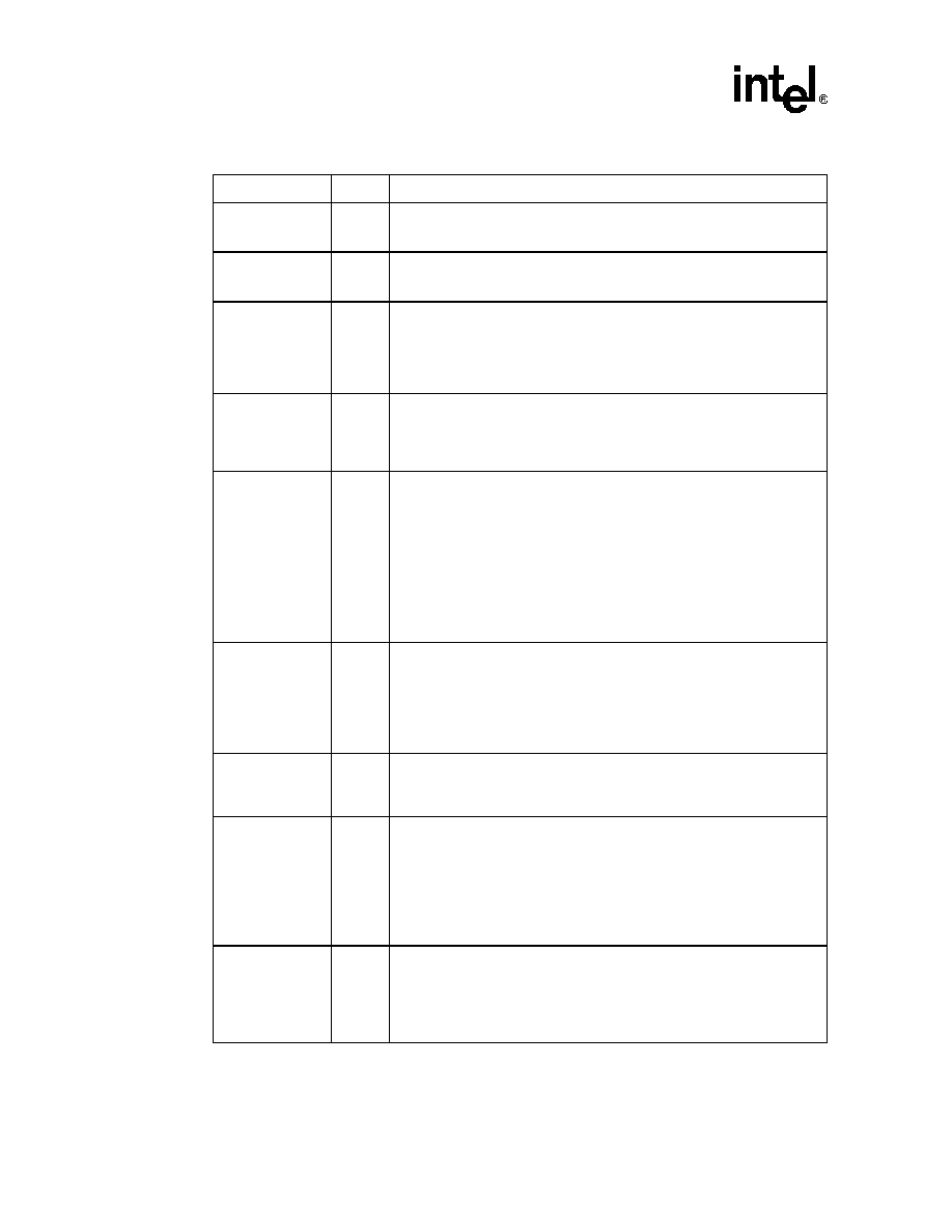
Intel
Æ
82801E C-ICH
30
Advance Information Datasheet
PDCS3#
O
Primary IDE Device Chip Select for 300 Range: This signal is for the ATA
control register block. This output signal is connected to the corresponding
signal on the primary IDE connector.
PDD[15:0]
I/O
Primary IDE Device Data: These signals directly drive the corresponding
signals on the primary IDE connector. There is a weak internal pull-down
resistor on PDD[7].
PDDACK#
O
Primary IDE Device DMA Acknowledge: This signal directly drives the
DAK# signal on the primary IDE connector. This signal is asserted by the
82801E C-ICH to indicate to the IDE DMA slave device that a given data
transfer cycle (assertion of DIOR# or DIOW#) is a DMA data transfer cycle.
This signal is used in conjunction with the PCI bus master IDE function and is
not associated with any AT-compatible DMA channel.
PDDREQ
I
Primary IDE Device DMA Request: This input signal is directly driven from
the DRQ signal on the primary IDE connector. It is asserted by the IDE device
to request a data transfer, and used in conjunction with the PCI bus master
IDE function. This signal is not associated with any AT-compatible DMA
channel. There is a weak internal pull-down resistor on PDDREQ.
PDIOR#
/(PDWSTB
/PRDMARDY#)
O
Primary Disk I/O Read (PIO and Non-Ultra DMA): This is the command to
the IDE device that it may drive data on the PDD lines. Data is latched by the
82801E C-ICH on the deassertion edge of PDIOR#. The IDE device is
selected either by the ATA register file chip selects (PDCS1#, PDCS3#) and
the PDA lines, or the IDE DMA acknowledge (PDDAK#).
Primary Disk Write Strobe (Ultra DMA Writes to Disk): PDWSTB is the
data write strobe for writes to disk. When writing to disk, the 82801E C-ICH
drives valid data on rising and falling edges of PDWSTB.
Primary Disk DMA Ready (Ultra DMA Reads from Disk): PRDMARDY# is
the DMA ready for reads from disk. When reading from disk, the 82801E
C-ICH deasserts PRDMARDY# to pause burst data transfers.
PDIOW#
/(PDSTOP)
O
Primary Disk I/O Write (PIO and Non-Ultra DMA): This is the command to
the IDE device that it may latch data from the PDD lines. Data is latched by
the IDE device on the deassertion edge of PDIOW#. The IDE device is
selected either by the ATA register file chip selects (PDCS1#, PDCS3#) and
the PDA lines, or the IDE DMA acknowledge (PDDAK#).
Primary Disk Stop (Ultra DMA): 82801E C-ICH asserts PDSTOP to
terminate a burst.
PERR#
I/O
Parity Error: An external PCI device drives PERR# when it receives data that
has a parity error. The 82801E C-ICH drives PERR# when it detects a parity
error. The ICH can either generate an NMI# or SMI# upon detecting a parity
error (either detected internally or reported via the PERR# signal).
PIORDY
/(PDRSTB
/PWDMARDY#)
I
Primary I/O Channel Ready (PIO): This signal keeps the strobe active
(PDIOR# on reads, PDIOW# on writes) longer than the minimum width. It
adds wait states to PIO transfers.
Primary Disk Read Strobe (Ultra DMA Reads from Disk):
When reading
from disk, the 82801E C-ICH latches data from the disk on rising and falling
edges of PDRSTB.
Primary Disk DMA Ready (Ultra DMA Writes to Disk): When writing to disk,
PWDMARDY# is deasserted by the disk to pause burst data transfers.
PIRQ[A:D]#
I/OD
PCI Interrupt Requests: In Non-APIC Mode the PIRQx# signals can be
routed to interrupts 3:7, 9:12, 14, or 15 as described in the Interrupt Steering
section. Each PIRQx# line has a separate Route Control Register.
In APIC mode, these signals are connected to the internal I/O APIC in the
following fashion: PIRQ[A]# is connected to IRQ16, PIRQ[B]# to IRQ17,
PIRQ[C]# to IRQ18, and PIRQ[D]# to IRQ19. This frees the ISA interrupts.
Table 6. 82801E C-ICH Signal Description (Sheet 6 of 11)
Signal
Type
Description
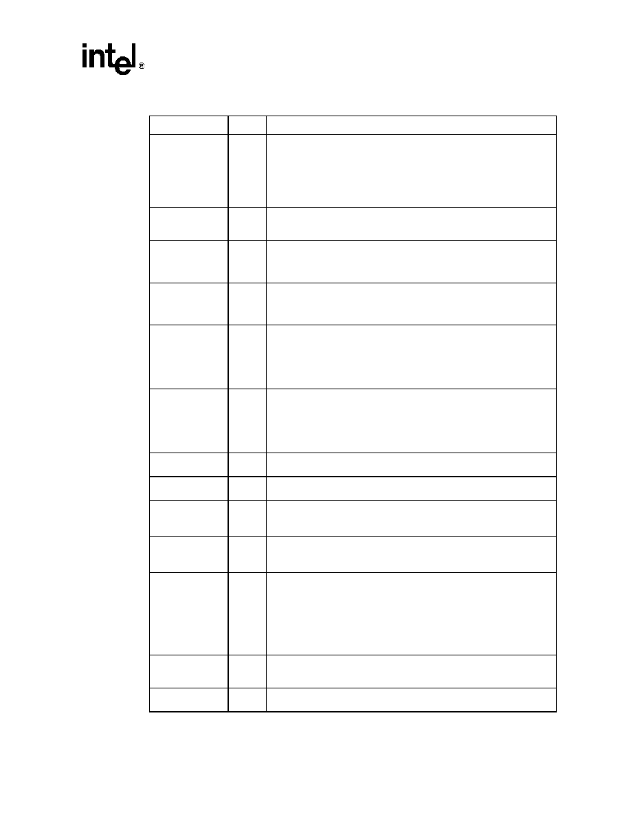
Intel
Æ
82801E C-ICH
Advance Information Datasheet
31
PIRQ[E:F]#
PIRQ[G]#/GPIO[4]
PIRQ[H]#/GPIO[5]
I/OD
PCI Interrupt Requests: In Non-APIC Mode the PIRQx# signals can be
routed to interrupts 3:7, 9:12, 14 or 15 as described in the Interrupt Steering
section. Each PIRQx# line has a separate Route Control Register.
In APIC mode, these signals are connected to the internal I/O APIC in the
following fashion: PIRQ[E]# is connected to IRQ20, PIRQ[F]# to IRQ21,
PIRQ[G]# to IRQ22, and PIRQ[H]# to IRQ23. If not needed for interrupts,
these signals can be used as GPIO.
PLOCK#
I/O
PCI Lock: PLOCK# indicates an exclusive bus operation and may require
multiple transactions to complete. 82801E C-ICH asserts PLOCK# when it
performs non-exclusive transactions on the PCI bus.
PWROK
I
Power OK: When asserted, PWROK is an indication to the 82801E C-ICH
that core power and PCICLK have been stable for at least 1 ms. PWROK can
be driven asynchronously. When PWROK is negated, the 82801E C-ICH
asserts PCIRST#.
RCIN#
I
Keyboard Controller Reset Processor: The keyboard controller can
generate INIT# to the processor. This saves the external OR gate with the
82801E C-ICH's other sources of INIT#. When the 82801E C-ICH detects the
assertion of this signal, INIT# is generated for 16 PCI clocks.
REQ[3:0]#
REQ[5]#
/REQ[B]#
/GPIO[1]
I
PCI Requests: The 82801E C-ICH supports up to four masters on the PCI
bus. REQ[5]# is muxed with PC/PCI REQ[B]# (must choose one or the other,
but not both). If not used for PCI or PC/PCI, REQ[5]#/REQ[B]# can instead be
used as GPIO[1].
NOTE: REQ[0]# is programmable to have improved arbitration latency for
supporting PCI-based 1394 controllers.
REQ[A]#
/GPIO[0]
REQ[B]#
/REQ[5]#
/GPIO[1]
I
PC/PCI DMA Request [A:B]: This request serializes ISA-like DMA Requests
for the purpose of running ISA-compatible DMA cycles over the PCI bus. This
is used by devices such as PCI-based Super I/O or audio codecs that need to
perform legacy 8237 DMA but have no ISA bus.
When not used for PC/PCI requests, these signals can be used as General
Purpose Inputs. Instead, REQ[B]# can be used as the fourth PCI bus request.
RESERVED1
RESERVED2
--
This signal must have an external pull up to Vcc3_3.
RI#
I
Ring Indicate: From the modem interface. This signal can be enabled as a
wake event; this is preserved across power failures.
RSM_PWROK
I
Resume Well Power OK: When asserted, this signal is an indication to the
82801E C-ICH that the resume well power has been stable for at least 10 ms.
NOTE: The 82801E C-ICH does not use the Resume Well Power OK signal.
RSMRST#
I
Resume Well Reset: RSMRST# is used for resetting the resume power
plane logic.
NOTE: The 82801E C-ICH does not use the Resume Well Reset signal.
RTCRST#
I
RTC Reset: When asserted, this signal resets register bits in the RTC well
and sets the RTC_PWR_STS bit (bit 2 in GEN_PMCON3 register). This
signal is also used to enter the test modes documented in "Test Signals" on
page 49.
NOTE: Clearing CMOS in an 82801E C-ICH-based platform can be done by
using a jumper on RTCRST# or GPI, or using SAFEMODE strap.
Implementations should not attempt to clear CMOS by using a
jumper to pull VccRTC low.
RTCX1
Special
Crystal Input 1: This signal is connected to the 32.768 KHz crystal. If no
external crystal is used, then RTCX1 can be driven with the desired clock
rate.
RTCX2
Special
Crystal Input 2: This signal is connected to the 32.768 KHz crystal. If no
external crystal is used, then RTCX2 should be left floating.
Table 6. 82801E C-ICH Signal Description (Sheet 7 of 11)
Signal
Type
Description

Intel
Æ
82801E C-ICH
32
Advance Information Datasheet
SDA[2:0]
O
Secondary IDE Device Address: These output signals are connected to the
corresponding signals on the secondary IDE connectors. They are used to
indicate which byte in either the ATA command block or control block is being
addressed.
SDCS1#
O
Secondary IDE Device Chip Selects for 100 Range: This signal is for the
ATA command register block. This output signal is connected to the
corresponding signal on the secondary IDE connector.
SDCS3#
O
Secondary IDE Device Chip Select for 300 Range: This signal is for the
ATA control register block. This output signal is connected to the
corresponding signal on the secondary IDE connector.
SDD[15:0]
I/O
Secondary IDE Device Data: These signals directly drive the corresponding
signals on the secondary IDE connector. There is a weak internal pull-down
resistor on SDD[7].
SDDACK#
O
Secondary IDE Device DMA Acknowledge: This signal directly drives the
DAK# signal on the secondary IDE connectors. This signal is asserted by the
82801E C-ICH to indicate to the IDE DMA slave device that a given data
transfer cycle (assertion of DIOR# or DIOW#) is a DMA data transfer cycle.
This signal is used in conjunction with the PCI bus master IDE function and is
not associated with any AT-compatible DMA channel.
SDDREQ
I
Secondary IDE Device DMA Request: This input signal is directly driven
from the DRQ signals on the secondary IDE connector. It is asserted by the
IDE device to request a data transfer, and used in conjunction with the PCI
bus master IDE function. It is not associated with any AT-compatible DMA
channel. There is a weak internal pull-down resistor on SDDREQ.
SDIOR#
/(SDWSTB/
SRDMARDY#)
O
Secondary Disk I/O Read (PIO and Non-Ultra DMA): This is the command
to the IDE device that it may drive data on the SDD lines. Data is latched by
the 82801E C-ICH on the deassertion edge of SDIOR#. The IDE device is
selected either by the ATA register file chip selects (SDCS1# or SDCS3#) and
the SDA lines, or the IDE DMA acknowledge (SDDAK#).
Secondary Disk Write Strobe (Ultra DMA Writes to Disk): This is the data
write strobe for writes to disk. When writing to disk, the 82801E C-ICH drives
valid data on rising and falling edges of SDWSTB.
Secondary Disk DMA Ready (Ultra DMA Reads from Disk): This is the
DMA ready for reads from disk. When reading from disk, the 82801E C-ICH
deasserts SRDMARDY# to pause burst data transfers.
SDIOW#
/(SDSTOP)
O
Secondary Disk I/O Write (PIO and Non-Ultra DMA): This is the command
to the IDE device that it may latch data from the SDD lines. Data is latched by
the IDE device on the deassertion edge of SDIOW#. The IDE device is
selected either by the ATA register file chip selects (SDCS1# or SDCS3#) and
the SDA lines, or the IDE DMA acknowledge (SDDAK#).
Secondary Disk Stop (Ultra DMA): The 82801E C-ICH asserts SDSTOP to
terminate a burst.
SERIRQ
I/O
Serial Interrupt Request: This pin implements the serial interrupt protocol.
SERR#
I
System Error: SERR# can be pulsed active by any PCI device that detects a
system error condition. Upon sampling SERR# active, the 82801E C-ICH has
the ability to generate an NMI, SMI#, or interrupt.
SIORDY
/(SDRSTB
/SWDMARDY#)
I
Secondary I/O Channel Ready (PIO): This signal keeps the strobe active
(SDIOR# on reads, SDIOW# on writes) longer than the minimum width. It
adds wait states to SIO transfers.
Secondary Disk Read Strobe (Ultra DMA Reads from Disk):
When reading
from disk, the 82801E C-ICH latches data from the disk on rising and falling
edges of SDRSTB.
Secondary Disk DMA Ready (Ultra DMA Writes to Disk): When writing to
disk, SWDMARDY# is deasserted by the disk to pause burst data transfers.
Table 6. 82801E C-ICH Signal Description (Sheet 8 of 11)
Signal
Type
Description

Intel
Æ
82801E C-ICH
Advance Information Datasheet
33
SIU_LAD[3:0]
I/O
SIU LPC Multiplexed Command, Address, Data: Internal pull-ups are
provided.
SIU_LCLK
I
SIU LPC clock input to SIU: 33 MHz LPC clock.
SIU_LDRQ#
O
SIU LPC Serial DMA/Master Request Output: Used by SIU devices to
indicate a DMA request. These signals have weak internal pull-up resistors to
avoid external glue.
SIU_LFRAME#
I
SIU LPC Frame: Indicates the start of an LPC cycle, or an abort.
SIU_RESET#
I
SIU Reset: This signal should be tied to PCI RESET.
SIU_SERIRQ
I/O
SIU Serial IRQ input: This pin receives the serial interrupt protocol from
external devices. Pull up if unused.
SIU0_CTS#
SIU1_CTS#
I
Clear To Send: Active low, this pin indicates that data can be exchanged
between CICH and external interface. These pins have no effect on the
transmitter.
NOTE: These pins could be used as Modem Status Input whose condition
can be tested by the processor by reading bit 4 (CTS) of the Modem
Status register (MSR). Bit 4 is the complement of the CTS# signal.
Bit 0 (DCTS) of the MSR indicates whether the CTS# input has
changed state since the previous reading of the MSR. When the CTS
bit of the MSR changes state an interrupt is generated if the Modem
Status Interrupt is enabled.
SIU0_DCD#
SIU1_DCD#
I
Data Carrier Detect for UART0 and UART1: Active low, this pin indicates
that data carrier has been detected by the external agent.
NOTE: These pins are Modem Status Inputs whose condition can be tested
by the processor by reading bit 7 (DCD) of the Modem Status register
(MSR). Bit 7 is the complement of the DCD# signal. Bit 3 (DDCD) of
the MSR indicates whether the DCD# input has changed state since
the previous reading of the MSR. When the DCD bit of the MSR
changes state an interrupt is generated if the Modem Status Interrupt
is enabled.
SIU0_DSR#
SIU1_DSR#
I
Data Set Ready for UART0 and UART1: Active low, this pin indicates that
the external agent is ready to communicate with 82801E C-ICH UARTs.
These pins have no effect on the transmitter.
NOTE: These pins could be used as Modem Status Inputs whose condition
can be tested by the processor by reading bit 5 (DSR) of the Modem
Status register. Bit 5 is the complement of the DSR# signal. Bit 1
(DDSR) of the Modem status register (MSR) indicates whether the
DSR# input has changed state since the previous reading of the
MSR. When the DSR bit of the MSR changes state an interrupt is
generated if the Modem Status Interrupt is enabled.
SIU0_DTR#
SIU1_DTR#
O
Data Terminal Ready for UART0 and UART1: When low these pins informs
the modem or data set that CICH UART 0, 1 are ready to establish a
communication link. The DTR#x(x=0,1) output signals can be set to an active
low by programming the DTRx (x-0,1) (bit0) of the Modem control register to a
logic `1'. A Reset operation sets this signal to its inactive state (logic `1').
LOOP mode operation holds this signal in its inactive state.
SIU0_RI#
SIU1_RI#
I
Ring Indicator for UART0 and UART1: Active low, this pin indicates that a
telephone ringing signal has been received by the external agent.
NOTE: These pins are Modem Status Input whose condition can be tested
by the processor by reading bit 6 (RI) of the Modem Status register
(MSR). Bit 6 is the complement of the RI# signal. Bit 2 (TERI) of the
MSR indicates whether the DCD# input has changed state since the
previous reading of the MSR. When the RI bit of the MSR changes
state an interrupt is generated if the Modem Status Interrupt is
enabled.
Table 6. 82801E C-ICH Signal Description (Sheet 9 of 11)
Signal
Type
Description
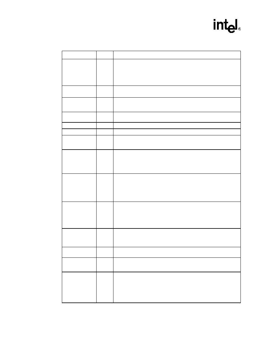
Intel
Æ
82801E C-ICH
34
Advance Information Datasheet
SIU0_RTS#
SIU1_RTS#
O
Request To Send for UART0 and UART1: When low these pins informs the
modem or data set that CICH UART 0, 1 are ready to establish a
communication link. The RTS#x(x=0,1) output signals can be set to an active
low by programming the RTSx (x-0,1) (bit1) of the Modem control register to a
logic `1'. A Reset operation sets this signal to its inactive state (logic `1').
LOOP mode operation holds this signal in its inactive state.
SIU0_RXD
SIU1_RXD
I
Serial Input for UART0 and UART1: Serial data input from device pin to the
receive port.
SIU0_TXD
SIU1_TXD
O
Serial Output for UART0 and UART1: Serial data output to the
communication peripheral/modem or data set. Upon reset, the TXD pins will
be set to MARKING condition (logic `1' state).
SMBALERT#
/GPIO[11]
I
SMBus Alert: This signal is used to wake the system or generate an SMI#. If
not used for SMBALERT#, it can be used as a GPI.
SMBCLK
I/OD
SMBus Clock: External pull-up is required.
SMBDATA
I/OD
SMBus Data: External pull-up is required.
SMI#
O
System Management Interrupt: SMI# is an active low output synchronous
to PCICLK. It is asserted by the 82801E C-ICH in response to one of many
enabled hardware or software events.
SMLINK[1:0]
I/OD
System Management Link: These signals are an SMBus link to an optional
external system management ASIC or LAN controller. External pull-ups are
required.
NOTE: SMLINK[0] corresponds to an SMBus Clock signal and SMLINK[1]
corresponds to an SMBus Data signal.
SPKR
O
Speaker: The SPKR signal is the output of counter 2 and is internally ANDed
with Port 61h bit 1 to provide Speaker Data Enable. This signal drives an
external speaker driver device, which in turn drives the system speaker. Upon
PCIRST#, its output state is 1.
NOTE: SPKR is sampled at the rising edge of PWROK as a functional strap.
See "Functional Straps" on page 49 for more details.
STOP#
I/O
Stop: STOP# indicates that the 82801E C-ICH, as a Target, is requesting the
Initiator to stop the current transaction. STOP# causes the 82801E C-ICH, as
an Initiator, to stop the current transaction. STOP# is an output when the
82801E C-ICH is a target and an input when the 82801E C-ICH is an Initiator.
STOP# is tri-stated from the leading edge of PCIRST#. STOP# remains
tri-stated until driven by the 82801E C-ICH.
STPCLK#
O
Stop Clock Request: STPCLK# is an active low output synchronous to
PCICLK. It is asserted by the 82801E C-ICH in response to one of many
hardware or software events. When the processor samples STPCLK#
asserted, it responds by stopping its internal clock.
SUSCLK
O
Suspend Clock: This signal is an output of the RTC generator circuit and is
used by other chips for the refresh clock.
THRM#
I
Thermal Alarm: THRM# is an active low signal generated by external
hardware to start the hardware clock throttling mode. This signal can also
generate an SMI# or an SCI.
TP[3:0]
I
Test Points:
TP0: This signal must have an external pull-up to Vcc3_3.
TP1: Route to a test point with option to jumper to Vcc1_8. Used for NAND
tree testing. Otherwise jumper to Vcc1_8.
TP2 and TP3: Route to a test point with option to jumper to V
SS
. Used for
NAND tree testing. Otherwise jumper to V
SS
.
Table 6. 82801E C-ICH Signal Description (Sheet 10 of 11)
Signal
Type
Description

Intel
Æ
82801E C-ICH
Advance Information Datasheet
35
TRDY#
I/O
Target Ready: TRDY# indicates the 82801E C-ICH's ability as a Target to
complete the current data phase of the transaction. TRDY# is used in
conjunction with IRDY#. A data phase is completed when both TRDY# and
IRDY# are sampled asserted. During a read, TRDY# indicates that the
82801E C-ICH, as a Target, has placed valid data on AD[31:0]. During a write,
TRDY# indicates the 82801E C-ICH, as a Target is prepared to latch data.
TRDY# is an input to the 82801E C-ICH when the 82801E C-ICH is the
Initiator and an output from the 82801E C-ICH when the 82801E C-ICH is a
Target. TRDY# is tri-stated from the leading edge of PCIRST#. TRDY#
remains tri-stated by the 82801E C-ICH until driven by a target.
UART_CLK
I
Input clock to the SIU. This clock is passed to the baud clock generation logic
of each UART in the SIU.
USBP0P
USBP0N
USBP1P
USBP1N
I/O
Universal Serial Bus Port 1:0 Differential: These differential pairs are used
to transmit Data/Address/Command signals for ports 0 and 1.
V_CPU_IO
Powered by the same supply as the processor I/O voltage. This supply is
used to drive the processor interface outputs.
V5REF
Reference for 5 V tolerance on Core well inputs.
VBIAS
RTC well bias voltage. The DC reference voltage applied to this pin sets a
current that is mirrored throughout the oscillator and buffer circuitry. See
"External RTC Circuitry" on page 50.
Vcc1_8
1.8 V supply for Core well logic.
Vcc3_3
3.3 V supply for Core well I/O buffers.
VccRTC
3.3 V (can drop to 2.0 V minimum in the G3 state) supply for the RTC well.
This power is not expected to be shut off unless the RTC battery is removed
or completely drained.
NOTE: Implementations should not attempt to clear CMOS by using a
jumper to pull VccRTC low. Clearing CMOS in an 82801E
C-ICH-based platform can be done by using a jumper on RTCRST#
or GPI, or using SAFEMODE strap.
VRMPWRGD
I
VRM Power Good: This can be considered to be the CPU's VRM power
good. This signal should be ANDed with the ATX power supply's PWROK
signal.
Vss
Grounds.
Table 6. 82801E C-ICH Signal Description (Sheet 11 of 11)
Signal
Type
Description
Intel
Æ
82801E C-ICH
36
Advance Information Datasheet
3.2
Signals Grouped By Type
3.2.1
Hub Interface to Host Controller
3.2.2
Link to LAN Connect
3.2.3
EEPROM Interface
Table 7. Hub Interface Signals
Name
Type
Description
HL[11:0]
I/O
Hub Interface Signals
HL_STB
I/O
Hub Interface Strobe: One of two differential strobe signals used to transmit and
receive data through the hub interface.
HL_STB#
I/O
Hub Interface Strobe Complement: Second of the two differential strobe signals.
HLCOMP
I/O
Hub Interface Compensation: Used for hub interface buffer compensation.
Table
8. LAN
Interface
Name
Type
Description
LAN0_CLK
LAN1_CLK
I
LAN Interface Clock: This signal is driven by the LAN Connect component. The
frequency range is 0.8 MHz to 50 MHz.
LAN0_RSTSYNC
LAN1_RSTSYNC
O
LAN Reset/Sync: The LAN Connect component's Reset and Sync signals are
multiplexed onto this pin.
LAN0_RXD[2:0]
LAN1_RXD[2:0]
I
Received Data: The LAN Connect component uses these signals to transfer
data and control information to the integrated LAN Controller. These signals
have integrated weak pull-up resistors.
LAN0_TXD[2:0]
LAN1_TXD[2:0]
O
Transmit Data: The integrated LAN Controller uses these signals to transfer
data and control information to the LAN Connect component.
Table 9. EEPROM Interface
Name
Type
Description
EE0_CS
EE1_CS
O
EEPROM Chip Select: These signals are chip-select signals to the EEPROMs.
EE0_DIN
EE1_DIN
I
EEPROM Data In: These signals transfer data from the EEPROMs to the 82801E
C-ICH. These signals have an integrated pull-up resistor.
EE0_DOUT
EE1_DOUT
O
EEPROM Data Out: These signals transfer data from the 82801E C-ICH to the
EEPROMs.
EE0_SHCLK
EE1_SHCLK
O
EEPROM Shift Clock: These signals are the serial shift clock output to the
EEPROMs.

Intel
Æ
82801E C-ICH
Advance Information Datasheet
37
3.2.4
Firmware Hub Interface
3.2.5
PCI Interface
Table 10. Firmware Hub Interface Signals
Name
Type
Description
FWH[3:0]
/LAD[3:0]
I/O
Firmware Hub Signals: These signals are muxed with LPC address signals.
FWH[4]
/LFRAME#
I/O
Firmware Hub Signals: This signal is muxed with the LPC LFRAME# signal.
Table 11. PCI Interface Signals (Sheet 1 of 3)
Name
Type
Description
AD[31:0]
I/O
PCI Address/Data: AD[31:0] is a multiplexed address and data bus. During the first
clock of a transaction, AD[31:0] contain a physical address (32 bits). During
subsequent clocks, AD[31:0] contain data. The 82801E C-ICH drives all 0s on
AD[31:0] during the address phase of all PCI Special Cycles.
C/BE[3:0]#
I/O
Bus Command and Byte Enables: The command and byte enable signals are
multiplexed on the same PCI pins. During the address phase of a transaction,
C/BE[3:0]# define the bus command. During the data phase, C/BE[3:0]# define the
Byte Enables.
C/BE[3:0]#
Command Type
0000
Interrupt Acknowledge
0001
Special Cycle
0010
I/O Read
0011
I/O Write
0110 Memory
Read
0111
Memory Write
1010 Configuration
Read
1011 Configuration
Write
1100
Memory Read Multiple
1101
DAC Mode Address to be latched (target only)
1110
Memory Read Line
1111
Memory Write and Invalidate
All command encodings not shown are reserved. The 82801E C-ICH does not
decode reserved values, and therefore will not respond if a PCI master generates a
cycle using one of the reserved values.
As a target, the 82801E C-ICH can support DAC mode addressing for 44 bits.
DEVSEL#
I/O
Device Select: The 82801E C-ICH asserts DEVSEL# to claim a PCI transaction.
As an output, the 82801E C-ICH asserts DEVSEL# when a PCI master peripheral
attempts an access to an internal 82801E C-ICH address or an address destined
for the hub interface (main memory or AGP). As an input, DEVSEL# indicates the
response to an 82801E C-ICH-initiated transaction on the PCI bus. DEVSEL# is
tri-stated from the leading edge of PCIRST#. DEVSEL# remains tri-stated by the
82801E C-ICH until driven by a target device.
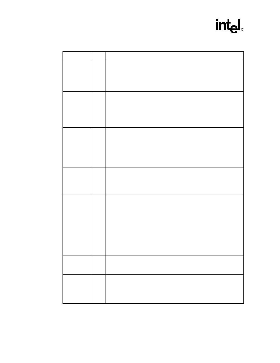
Intel
Æ
82801E C-ICH
38
Advance Information Datasheet
FRAME#
I/O
Cycle Frame: The current Initiator drives FRAME# to indicate the beginning and
duration of a PCI transaction. While the initiator asserts FRAME#, data transfers
continue. When the initiator negates FRAME#, the transaction is in the final data
phase. FRAME# is an input to the 82801E C-ICH when the 82801E C-ICH is the
target, and FRAME# is an output from the 82801E C-ICH when the 82801E C-ICH
is the Initiator. FRAME# remains tri-stated by the 82801E C-ICH until driven by an
Initiator.
IRDY#
I/O
Initiator Ready: IRDY# indicates the 82801E C-ICH's ability, as an Initiator, to
complete the current data phase of the transaction. It is used in conjunction with
TRDY#. A data phase is completed on any clock both IRDY# and TRDY# are
sampled asserted. During a write, IRDY# indicates the 82801E C-ICH has valid
data present on AD[31:0]. During a read, it indicates the 82801E C-ICH is prepared
to latch data. IRDY# is an input to the 82801E C-ICH when the 82801E C-ICH is the
Target and an output from the 82801E C-ICH when the 82801E C-ICH is an
Initiator. IRDY# remains tri-stated by the 82801E C-ICH until driven by an Initiator.
TRDY#
I/O
Target Ready: TRDY# indicates the 82801E C-ICH's ability as a Target to complete
the current data phase of the transaction. TRDY# is used in conjunction with
IRDY#. A data phase is completed when both TRDY# and IRDY# are sampled
asserted. During a read, TRDY# indicates that the 82801E C-ICH, as a Target, has
placed valid data on AD[31:0]. During a write, TRDY# indicates the 82801E C-ICH,
as a Target is prepared to latch data. TRDY# is an input to the 82801E C-ICH when
the 82801E C-ICH is the Initiator and an output from the 82801E C-ICH when the
82801E C-ICH is a Target. TRDY# is tri-stated from the leading edge of PCIRST#.
TRDY# remains tri-stated by the 82801E C-ICH until driven by a target.
STOP#
I/O
Stop: STOP# indicates that the 82801E C-ICH, as a Target, is requesting the
Initiator to stop the current transaction. STOP# causes the 82801E C-ICH, as an
Initiator, to stop the current transaction. STOP# is an output when the 82801E
C-ICH is a target and an input when the 82801E C-ICH is an Initiator. STOP# is
tri-stated from the leading edge of PCIRST#. STOP# remains tri-stated until driven
by the 82801E C-ICH.
PAR
I/O
Calculated/Checked Parity: PAR uses "even" parity calculated on 36 bits,
AD[31:0] plus C/BE[3:0]#. "Even" parity means that the 82801E C-ICH counts the
number of 1s within the 36 bits plus PAR and the sum is always even. The 82801E
C-ICH always calculates PAR on 36 bits, regardless of the valid byte enables. The
82801E C-ICH generates PAR for address and data phases and only guarantees
PAR to be valid one PCI clock after the corresponding address or data phase. The
82801E C-ICH drives and tri-states PAR identically to the AD[31:0] lines except that
the 82801E C-ICH delays PAR by exactly one PCI clock. PAR is an output during
the address phase (delayed one clock) for all 82801E C-ICH initiated transactions.
PAR is an output during the data phase (delayed one clock) when the 82801E
C-ICH is the Initiator of a PCI write transaction, and when it is the target of a read
transaction. 82801E C-ICH checks parity when it is the target of a PCI write
transaction. If a parity error is detected, the 82801E C-ICH sets the appropriate
internal status bits, and has the option to generate an NMI# or SMI#.
PERR#
I/O
Parity Error: An external PCI device drives PERR# when it receives data that has
a parity error. The 82801E C-ICH drives PERR# when it detects a parity error. The
ICH can either generate an NMI# or SMI# upon detecting a parity error (either
detected internally or reported via the PERR# signal).
REQ[3:0]#
/REQ[5]#
/REQ[B]#
/GPIO[1]
I
PCI Requests: The 82801E C-ICH supports up to five masters on the PCI bus.
REQ[5]# is muxed with PC/PCI REQ[B]# (must choose one or the other, but not
both). If not used for PCI or PC/PCI, REQ[5]#/REQ[B]# can instead be used as
GPIO[1].
NOTE: REQ[0]# is programmable to have improved arbitration latency for
supporting PCI-based 1394 controllers.
Table 11. PCI Interface Signals (Sheet 2 of 3)
Name
Type
Description

Intel
Æ
82801E C-ICH
Advance Information Datasheet
39
GNT[3:0]#
/GNT[5]#
/GNT[B]#
/GPIO[17]#
O
PCI Grants: The 82801E C-ICH supports up to four masters on the PCI bus.
Pull-up resistors are not required on these signals. If pullups are used, they should
be tied to the Vcc3_3 power rail. GNT[B]#/GNT[5]#/GPIO[17] has an internal
pull-up.
PCICLK
I
PCI Clock: This is a 33 MHz clock. PCICLK provides timing for all transactions on
the PCI Bus.
PCIRST#
O
PCI Reset: 82801E C-ICH asserts PCIRST# to reset devices that reside on the PCI
bus. The 82801E C-ICH asserts PCIRST# during power-up and when S/W initiates
a hard reset sequence through the RC (CF9h) register. The 82801E C-ICH drives
PCIRST# inactive a minimum of 1 ms after PWROK is driven active. The 82801E
C-ICH drives PCIRST# active a minimum of 1 ms when initiated through the RC
register.
PLOCK#
I/O
PCI Lock: PLOCK# indicates an exclusive bus operation and may require multiple
transactions to complete. 82801E C-ICH asserts PLOCK# when it performs
non-exclusive transactions on the PCI bus.
SERR#
I
System Error: SERR# can be pulsed active by any PCI device that detects a
system error condition. Upon sampling SERR# active, the 82801E C-ICH has the
ability to generate an NMI, SMI#, or interrupt.
REQ[A]#
/GPIO[0]
REQ[B]#
/REQ[5]#
/GPIO[1]
I
PC/PCI DMA Request [A:B]: This request serializes ISA-like DMA Requests for
the purpose of running ISA-compatible DMA cycles over the PCI bus. This is used
by devices such as PCI-based Super I/O or audio codecs that need to perform
legacy 8237 DMA but have no ISA bus.
When not used for PC/PCI requests, these signals can be used as General
Purpose Inputs. Instead, REQ[B]# can be used as the fifth PCI bus request.
GNT[A]#
/GPIO[16]
GNT[B]#
/GNT[5]#
/GPIO[17]
O
PC/PCI DMA Acknowledges [A:B]: This grant serializes an ISA-like DACK# for
the purpose of running DMA/ISA master cycles over the PCI bus. This is used by
devices such as PCI-based Super/IO or audio codecs which need to perform
legacy 8237 DMA but have no ISA bus.
When not used for PC/PCI, these signals can be used as General Purpose
Outputs. GNTB# can also be used as the fifth PCI bus master grant output. These
signal have internal pull-up resistors.
Table 11. PCI Interface Signals (Sheet 3 of 3)
Name
Type
Description

Intel
Æ
82801E C-ICH
40
Advance Information Datasheet
3.2.6
IDE Interface
Table 12. IDE Interface Signals
Name
Type
Description
PDCS1#
SDCS1#
O
Primary and Secondary IDE Device Chip Selects for 100 Range: These
signals are for the ATA command register block. This output signal is connected
to the corresponding signal on the primary or secondary IDE connector.
PDCS3#
SDCS3#
O
Primary and Secondary IDE Device Chip Select for 300 Range: These signals
are for the ATA control register block. This output signal is connected to the
corresponding signal on the primary or secondary IDE connector.
PDA[2:0]
SDA[2:0]
O
Primary and Secondary IDE Device Address: These output signals are
connected to the corresponding signals on the primary or secondary IDE
connectors. They are used to indicate which byte in either the ATA command
block or control block is being addressed.
PDD[15:0]
SDD[15:0]
I/O
Primary and Secondary IDE Device Data: These signals directly drive the
corresponding signals on the primary or secondary IDE connector. There is a
weak internal pull-down resistor on PDD[7] and SDD[7].
PDDREQ
SDDREQ
I
Primary and Secondary IDE Device DMA Request: These input signals are
directly driven from the DRQ signals on the primary or secondary IDE connector.
It is asserted by the IDE device to request a data transfer, and used in
conjunction with the PCI bus master IDE function. They are not associated with
any AT-compatible DMA channel. There is a weak internal pull-down resistor on
these signals.
PDDACK#
SDDACK#
O
Primary and Secondary IDE Device DMA Acknowledge: These signals
directly drive the DAK# signals on the primary and secondary IDE connectors.
Each signal is asserted by the 82801E C-ICH to indicate to the IDE DMA slave
devices that a given data transfer cycle (assertion of DIOR# or DIOW#) is a DMA
data transfer cycle. This signal is used in conjunction with the PCI bus master
IDE function and are not associated with any AT-compatible DMA channel.
PDIOR#
/(PDWSTB
/PRDMARDY#)
SDIOR#
/(SDWSTB
/SRDMARDY#)
O
Primary and Secondary Disk I/O Read (PIO and Non-Ultra DMA): This is the
command to the IDE device that it may drive data on the PDD or SDD lines. Data
is latched by the 82801E C-ICH on the deassertion edge of PDIOR# or SDIOR#.
The IDE device is selected either by the ATA register file chip selects (PDCS1# or
SDCS1#, PDCS3# or SDCS3#) and the PDA or SDA lines, or the IDE DMA
acknowledge (PDDAK# or SDDAK#).
Primary and Secondary Disk Write Strobe (Ultra DMA Writes to Disk): This is
the data write strobe for writes to disk. When writing to disk, 82801E C-ICH drives
valid data on rising and falling edges of PDWSTB or SDWSTB.
Primary and Secondary Disk DMA Ready (Ultra DMA Reads from Disk): This
is the DMA ready for reads from disk. When reading from disk, 82801E C-ICH
deasserts PRDMARDY# or SRDMARDY# to pause burst data transfers.
PDIOW#
/(PDSTOP)
SDIOW#
/(SDSTOP)
O
Primary and Secondary Disk I/O Write (PIO and Non-Ultra DMA): This is the
command to the IDE device that it may latch data from the PDD or SDD lines.
Data is latched by the IDE device on the deassertion edge of PDIOW# or
SDIOW#. The IDE device is selected either by the ATA register file chip selects
(PDCS1# or SDCS1#, PDCS3# or SDCS3#) and the PDA or SDA lines, or the
IDE DMA acknowledge (PDDAK# or SDDAK#).
Primary and Secondary Disk Stop (Ultra DMA): 82801E C-ICH asserts this
signal (PDSTOP, SDSTOP) to terminate a burst.
PIORDY
/(PDRSTB
/PWDMARDY#)
SIORDY
/(SDRSTB
/SWDMARDY#)
I
Primary and Secondary I/O Channel Ready (PIO): This signal keeps the strobe
active (PDIOR# or SDIOR# on reads, PDIOW# or SDIOW# on writes) longer than
the minimum width. It adds wait states to PIO transfers.
Primary and Secondary Disk Read Strobe (Ultra DMA Reads from Disk):
When reading from disk, 82801E C-ICH latches data on rising and falling edges
of this signal from the disk.
Primary and Secondary Disk DMA Ready (Ultra DMA Writes to Disk): When
writing to disk, this is deasserted by the disk to pause burst data transfers.
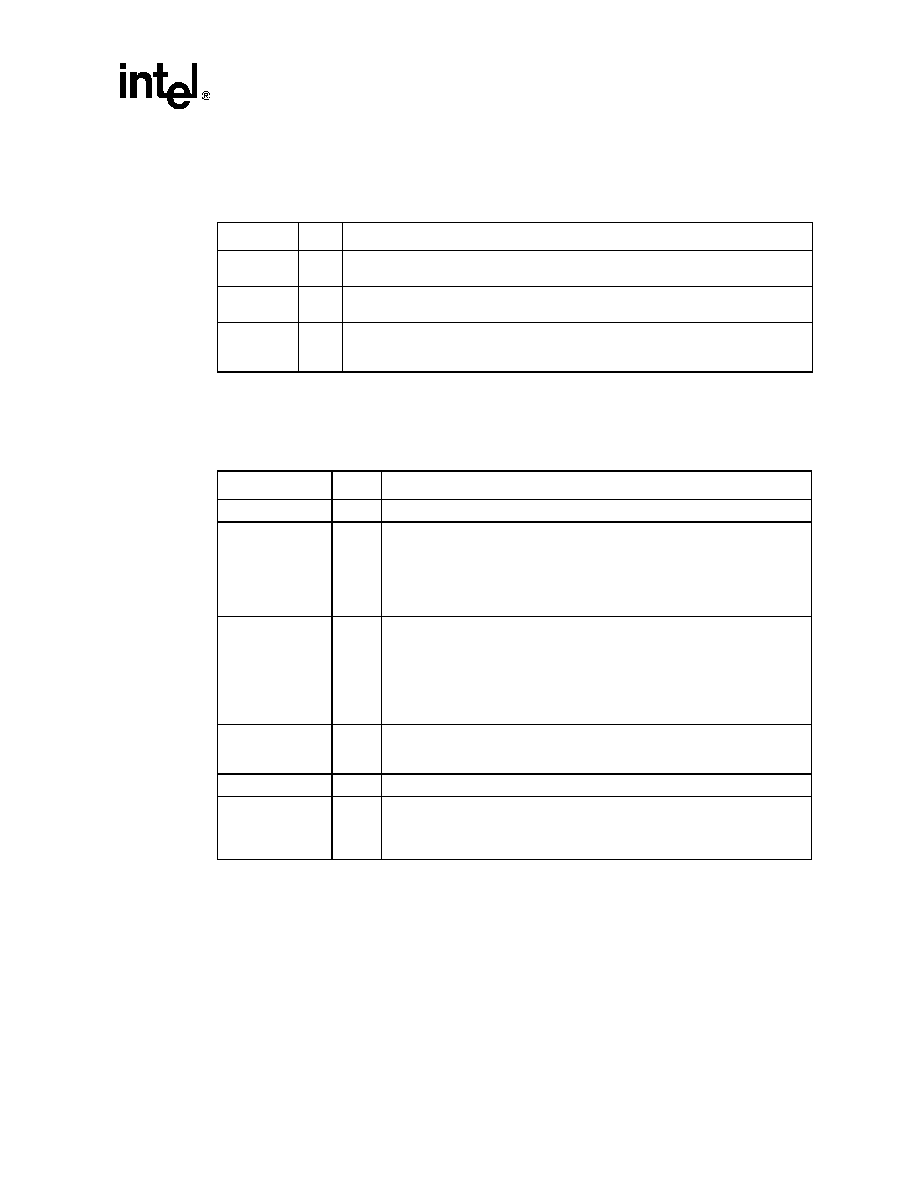
Intel
Æ
82801E C-ICH
Advance Information Datasheet
41
3.2.7
LPC Interface
3.2.8
Interrupt Interface
Table 13. LPC Interface Signals
Name
Type
Description
LAD[3:0]
/FWH[3:0]
I/O
LPC Multiplexed Command, Address, Data: Internal pull-ups are provided.
LFRAME#
/FWH[4]
O
LPC Frame: LFRAME# indicates the start of an LPC cycle, or an abort.
LDRQ[1:0]#
I
LPC Serial DMA/Master Request Inputs: These signals are used to request DMA or
bus master access. Typically, they are connected to external Super I/O device. An
internal pull-up resistor is provided on these signals.
Table 14. Interrupt Signals
Name
Type
Description
SERIRQ
I/O
Serial Interrupt Request: This pin implements the serial interrupt protocol.
PIRQ[A:D]#
I/OD
PCI Interrupt Requests: In Non-APIC Mode the PIRQx# signals can be routed
to interrupts 3:7, 9:12, 14, or 15 as described in the Interrupt Steering section.
Each PIRQx# line has a separate Route Control Register.
In APIC mode, these signals are connected to the internal I/O APIC in the
following fashion: PIRQ[A]# is connected to IRQ16, PIRQ[B]# to IRQ17,
PIRQ[C]# to IRQ18, and PIRQ[D]# to IRQ19. This frees the ISA interrupts.
PIRQ[E:F]#
PIRQ[G]#/GPIO[4]
PIRQ[H]#/GPIO[5]
I/OD
PCI Interrupt Requests: In Non-APIC Mode the PIRQx# signals can be routed
to interrupts 3:7, 9:12, 14 or 15 as described in the Interrupt Steering section.
Each PIRQx# line has a separate Route Control Register.
In APIC mode, these signals are connected to the internal I/O APIC in the
following fashion: PIRQ[E]# is connected to IRQ20, PIRQ[F]# to IRQ21,
PIRQ[G]# to IRQ22, and PIRQ[H]# to IRQ23. This frees the ISA interrupts. If
not needed for interrupts, PIRQ[H:G] can be used as GPIO.
IRQ[14:15]
I
Interrupt Request 14:15: These interrupt inputs are connected to the IDE
drives. IRQ14 is used by the drives connected to the primary controller and
IRQ15 is used by the drives connected to the secondary controller.
APICCLK
I
APIC Clock: The APIC clock runs at 33.333 MHz.
APICD[1:0]
I/OD
APIC Data: These bidirectional open drain signals are used to send and
receive data over the APIC bus. As inputs, the data is valid on the rising edge
of APICCLK. As outputs, new data is driven from the rising edge of the
APICCLK.
Intel
Æ
82801E C-ICH
42
Advance Information Datasheet
3.2.9
USB Interface
3.2.10
Power Signals
Table 15. USB Interface Signals
Name
Type
Description
USBP0P
USBP0N
USBP1P
USBP1N
I/O
Universal Serial Bus Port 1:0 Differential: These differential pairs are used to
transmit Data/Address/Command signals for ports 0 and 1.
OC[1:0]#
I
Overcurrent Indicators: These signals set corresponding bits in the USB
controllers to indicate that an overcurrent condition has occurred.
Table 16. Power Signals
Name
Type
Description
PWROK
I
Power OK: When asserted, PWROK is an indication to the 82801E C-ICH that
core power and PCICLK have been stable for at least 1 ms. PWROK can be driven
asynchronously. When PWROK is negated, the 82801E C-ICH asserts PCIRST#.
RSM_PWROK
I
Resume Well Power OK: When asserted, this signal is an indication to the
82801E C-ICH that the resume well power has been stable for at least 10 ms.
NOTE: The 82801E C-ICH does not use the resume well power OK signal.
RSMRST#
I
Resume Well Reset: RSMRST# is used for resetting the resume power plane
logic.
NOTE: The 82801E C-ICH does not use the resume well reset signal.
VRMPWRGD
I
VRM Power Good: VRMPWRGD should be connected to be the processor's VRM
Power Good.
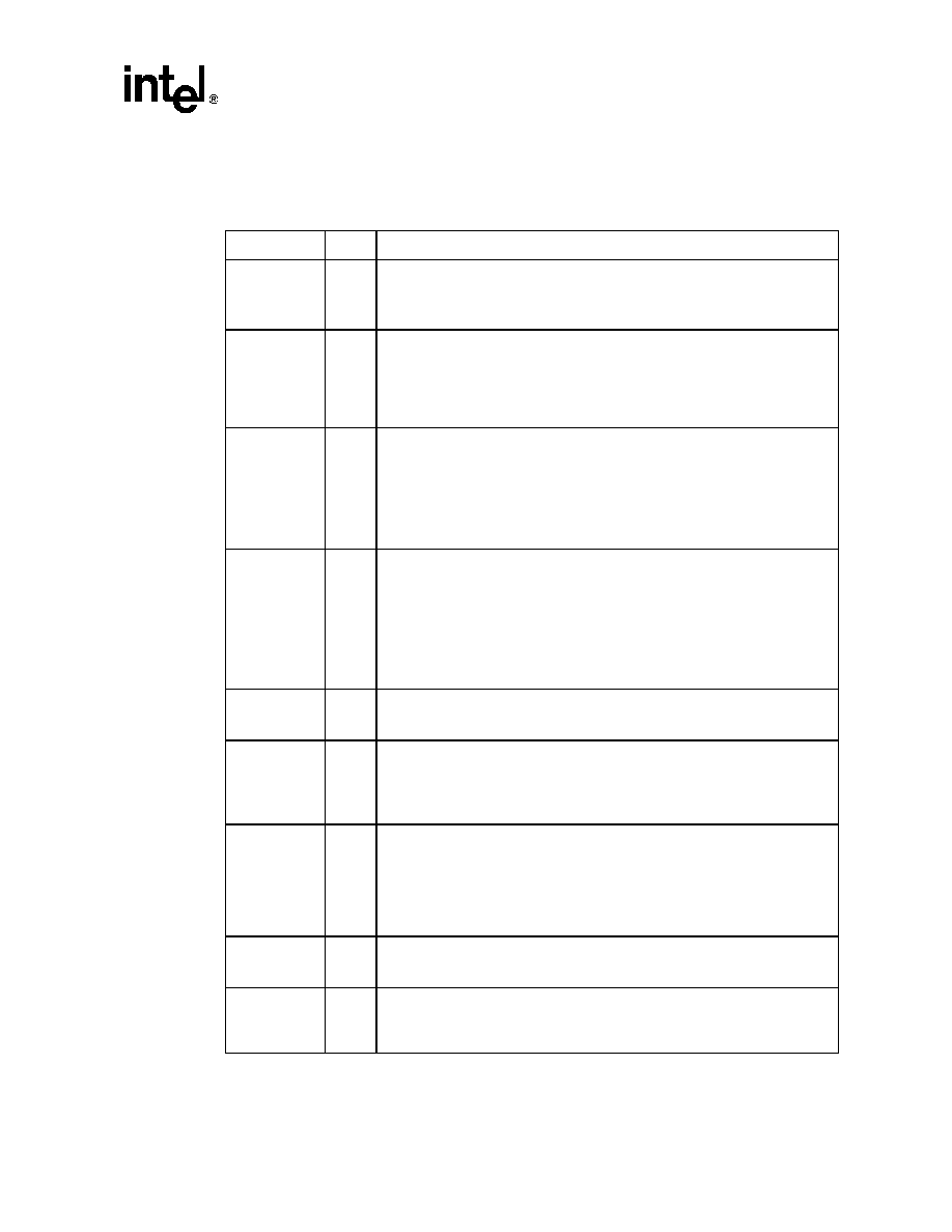
Intel
Æ
82801E C-ICH
Advance Information Datasheet
43
3.2.11
Processor Interface
Table 17. Processor Interface Signals (Sheet 1 of 2)
Name
Type
Description
A20M#
O
Mask A20: A20M# goes active based on setting the appropriate bit in the Port 92h
register, or based on the A20GATE signal.
Speed Strap: During the reset sequence, 82801E C-ICH drives A20M# high if the
corresponding bit is set in the FREQ_STRP register.
CPUSLP#
O
Processor Sleep: This signal puts the processor into a state that saves
substantial power compared to Stop-Grant state. However, during that time, no
snoops occur. The 82801E C-ICH can optionally assert the CPUSLP# signal when
going to the S1 state.
NOTE: The 82801E C-ICH does not support Sleep states. This signal must be
pulled up through an 8.2 K
resistor to 3.3 V.
FERR#
I
Numeric Coprocessor Error: This signal is tied to the coprocessor error signal
on the processor. FERR# is only used if the 82801E C-ICH coprocessor error
reporting function is enabled in the General Control Register (Device 31:Function
0, Offset D0, bit 13). If FERR# is asserted, the 82801E C-ICH generates an
internal IRQ13 to its interrupt controller unit. It is also used to gate the IGNNE#
signal to ensure that IGNNE# is not asserted to the processor unless FERR# is
active. FERR# requires an external weak pull-up to ensure a high level when the
coprocessor error function is disabled.
IGNNE#
O
Ignore Numeric Error: This signal is connected to the ignore error pin on the
processor. IGNNE# is only used if the 82801E C-ICH coprocessor error reporting
function is enabled in the General Control Register (Device 31:Function 0, Offset
D0, bit 13). If FERR# is active, indicating a coprocessor error, a write to the
Coprocessor Error Register (F0h) causes the IGNNE# to be asserted. IGNNE#
remains asserted until FERR# is negated. If FERR# is not asserted when the
Coprocessor Error Register is written, the IGNNE# signal is not asserted.
Speed Strap: During the reset sequence, 82801E C-ICH drives IGNNE# high if
the corresponding bit is set in the FREQ_STRP register.
INIT#
O
Initialization: INIT# is asserted by the 82801E C-ICH for 16 PCI clocks to reset
the processor. 82801E C-ICH can be configured to support processor BIST. In that
case, INIT# will be active when PCIRST# is active.
INTR
O
Processor Interrupt: INTR is asserted by the 82801E C-ICH to signal the
processor that an interrupt request is pending and needs to be serviced. It is an
asynchronous output and normally driven low.
Speed Strap: During the reset sequence, 82801E C-ICH drives INTR high if the
corresponding bit is set in the FREQ_STRP register.
NMI
O
Non-Maskable Interrupt: NMI is used to force a non-maskable interrupt to the
processor. The 82801E C-ICH can generate an NMI when either SERR# or
IOCHK# is asserted. The processor detects an NMI when it detects a rising edge
on NMI. NMI is reset by setting the corresponding NMI source enable/disable bit in
the NMI Status and Control Register.
Speed Strap: During the reset sequence, 82801E C-ICH drives NMI high if the
corresponding bit is set in the FREQ_STRP register.
SMI#
O
System Management Interrupt: SMI# is an active low output synchronous to
PCICLK. It is asserted by the 82801E C-ICH in response to one of many enabled
hardware or software events.
STPCLK#
O
Stop Clock Request: STPCLK# is an active low output synchronous to PCICLK.
It is asserted by the 82801E C-ICH in response to one of many hardware or
software events. When the processor samples STPCLK# asserted, it responds by
stopping its internal clock.

Intel
Æ
82801E C-ICH
44
Advance Information Datasheet
3.2.12
SMBus Interface
3.2.13
System Management Interface
3.2.14
Real Time Clock Interface
RCIN#
I
Keyboard Controller Reset Processor: The keyboard controller can generate
INIT# to the processor. This saves the external OR gate with the 82801E C-ICH's
other sources of INIT#. When the 82801E C-ICH detects the assertion of this
signal, INIT# is generated for 16 PCI clocks.
A20GATE
I
A20 Gate: This signal is from the keyboard controller. It acts as an alternative
method to force the A20M# signal active. A20GATE saves the external OR gate
needed with various other PCIsets.
CPUPWRGD
OD
Processor Power Good: This signal should be connected to the processor's
PWRGOOD input. This is an open-drain output signal (external pull-up resistor
required) that represents a logical AND of the 82801E C-ICH's PWROK and
VRMPWRGD signals.
Table 18. SMBus Interface Signals
Name
Type
Description
SMBDATA
I/OD
SMBus Data: External pull-up is required.
SMBCLK
I/OD
SMBus Clock: External pull-up is required.
SMBALERT#
/GPIO[11]
I
SMBus Alert: This signal is used to wake the system or generate an SMI#. If not
used for SMBALERT#, it can be used as a GPI.
Table 19. System Management Interface Signals
Name
Type
Description
INTRUDER#
I
Intruder Detect: This signal can be set to disable system if box detected open.
This signal's status is readable, so it can be used like a GPI if the Intruder
Detection is not needed.
SMLINK[1:0]
I/OD
System Management Link: These signals are an SMBus link to an optional
external system management ASIC or LAN controller. External pull-ups are
required.
NOTE: SMLINK[0] corresponds to an SMBus Clock signal and SMLINK[1]
corresponds to an SMBus Data signal.
Table 20. Real Time Clock Interface
Name
Type
Description
RTCX1
Special
Crystal Input 1: This signal is connected to the 32.768 KHz crystal. If no
external crystal is used, then RTCX1 can be driven with the desired clock rate.
RTCX2
Special
Crystal Input 2: This signal is connected to the 32.768 KHz crystal. If no
external crystal is used, then RTCX2 should be left floating.
Table 17. Processor Interface Signals (Sheet 2 of 2)
Name
Type
Description

Intel
Æ
82801E C-ICH
Advance Information Datasheet
45
3.2.15
Other Clocks
3.2.16
Universal Asynchronous Receive and Transmit (UART 0,1)
Table 21. Other Clocks
Name
Type
Description
CLK14
I
Oscillator Clock: CLK14 is used for 8254 timers and runs at 14.31818 MHz.
CLK48
I
48 MHz Clock: CLK48 is used to for the USB controller and runs at 48 MHz.
CLK66
(HLCLK)
I
66 MHz Clock (HLCLK): CLK66 is used for the hub interface and runs at 66 MHz.
Table 22. Universal Asynchronous Receive And Transmit (UART 0, 1) (Sheet 1 of 2)
Signal Name
Type
Description
UART_CLK
I
Input clock to the SIU. This clock is passed to the baud clock generation logic of
each UART in the SIU.
SIU0_CTS#
SIU1_CTS#
I
Clear to Send: Active low, this pin indicates that data can be exchanged
between CICH and external interface. These pins have no effect on the
transmitter.
NOTE: These pins could be used as Modem Status Inputs whose condition can
be tested by the processor by reading bit 4 (CTS) of the Modem Status
register (MSR). Bit 4 is the complement of the CTS# signal. Bit 0
(DCTS) of the MSR indicates whether the CTS# input has changed state
since the previous reading of the MSR. When the CTS bit of the MSR
changes state an interrupt is generated if the Modem Status Interrupt is
enabled.
SIU0_DCD#
SIU1_DCD#
I
Data Carrier Detect for UART0 and UART1: Active low, this pin indicates that
data carrier has been detected by the external agent.
NOTE: These pins are Modem Status Inputs whose condition can be tested by
the processor by reading bit 7 (DCD) of the Modem Status register
(MSR). Bit 7 is the complement of the DCD# signal. Bit 3 (DDCD) of the
MSR indicates whether the DCD# input has changed state since the
previous reading of the MSR. When the DCD bit of the MSR changes
state an interrupt is generated if the Modem Status Interrupt is enabled.
SIU0_DSR#
SIU1_DSR#
I
Data Set Ready for UART0 and UART1: Active low, this pin indicates that the
external agent is ready to communicate with 82801E C-ICH UARTs. These pins
have no effect on the transmitter.
NOTE: These pins could be used as Modem Status Input whose condition can
be tested by the processor by reading bit 5 (DSR) of the Modem Status
register. Bit 5 is the complement of the DSR# signal. Bit 1 (DDSR) of the
Modem status register (MSR) indicates whether the DSR# input has
changed state since the previous reading of the MSR. When the DSR bit
of the MSR changes state an interrupt is generated if the Modem Status
Interrupt is enabled.
SIU0_DTR#
SIU1_DTR#
O
Data Terminal Ready for UART0 and UART1: When low these pins informs the
modem or data set that 82801E C-ICH UART0 and UART1 are ready to establish
a communication link. The DTR#x(x=0,1) output signals can be set to an active
low by programming the DTRx (x-0,1) (bit0) of the Modem control register to a
logic `1'. A Reset operation sets this signal to its inactive state (logic `1'). LOOP
mode operation holds this signal in its inactive state.
Intel
Æ
82801E C-ICH
46
Advance Information Datasheet
3.2.17
SIU LPC Interface
SIU0_RI#
SIU1_RI#
I
Ring Indicator for UART0 and UART1: Active low, this pin indicates that a
telephone ringing signal has been received by the external agent.
NOTE: These pins are Modem Status Input whose condition can be tested by
the processor by reading bit 6 (RI) of the Modem Status register (MSR).
Bit 6 is the complement of the RI# signal. Bit 2 (TERI) of the MSR
indicates whether the DCD# input has changed state since the previous
reading of the MSR. When the RI bit of the MSR changes state an
interrupt is generated if the Modem Status Interrupt is enabled.
SIU0_RTS#
SIU1_RTS#
O
Request to Send for UART0 and UART1: When low these pins informs the
modem or data set that 82801E C-ICH UART0 and UART1 are ready to establish
a communication link. The RTS#x(x=0,1) output signals can be set to an active
low by programming the RTSx (x-0,1) (bit1) of the Modem control register to a
logic `1'. A Reset operation sets this signal to its inactive state (logic `1'). LOOP
mode operation holds this signal in its inactive state.
SIU0_RXD
SIU1_RXD
I
Serial Inputs for UART0 and UART1: Serial data input from device pin to the
receive port.
SIU0_TXD
SIU1_TXD
O
Serial Output for UART0 and UART1: Serial data output to the communication
peripheral/modem or data set. Upon reset, the TXD pins will be set to MARKING
condition (logic `1' state).
Table 23. SIU Interface
Signal Name
Type
Description
SIU_LAD[3:0]
I/O
SIU LPC Multiplexed Command, Address, Data: Internal pull-ups are provided.
SIU_LCLK
I
SIU LPC clock input to SIU: 33 MHz LPC clock.
SIU_LDRQ#
O
SIU LPC Serial DMA/Master Request Output: Used by SIU devices to indicate a
DMA request.
NOTE: These signals have weak internal pull-up resistors to avoid external glue.
SIU_LFRAME#
I
SIU LPC Frame: Indicates the start of an LPC cycle, or an abort.
SIU_RESET#
I
SIU RESET: This signal should be tied to PCI RESET.
SIU_SERIRQ
I/O
SIU Serial IRQ input: This pin receives the serial interrupt protocol from external
devices. Pull up if unused.
Table 22. Universal Asynchronous Receive And Transmit (UART 0, 1) (Sheet 2 of 2)
Signal Name
Type
Description

Intel
Æ
82801E C-ICH
Advance Information Datasheet
47
3.2.18
Miscellaneous Signals
3.2.19
General Purpose I/O
Table 24. Miscellaneous Signals
Name
Type
Description
HL[11]
I
No pull-up required. Use a no-stuff or a test point for NAND tree testing.
RTCRST#
I
RTC Reset: When asserted, this signal resets register bits in the RTC well and
sets the RTC_PWR_STS bit (bit 2 in GEN_PMCON3 register). This signal is also
used to enter the test modes documented in "Test Signals" on page 49.
NOTE: Clearing CMOS in an 82801E C-ICH-based platform can be done by
using a jumper on RTCRST# or GPI, or using SAFEMODE strap.
Implementations should not attempt to clear CMOS by using a jumper to
pull VccRTC low.
SPKR
O
Speaker: The SPKR signal is the output of counter 2 and is internally ANDed with
Port 61h bit 1 to provide Speaker Data Enable. This signal drives an external
speaker driver device, which in turn drives the system speaker. Upon PCIRST#, its
output state is 1.
NOTE: SPKR is sampled at the rising edge of PWROK as a functional strap. See
"Functional Straps" on page 49for more details.
TP0
I
Test Point 0: This signal must have an external pull-up to Vcc3_3.
THRM#
I
Thermal Alarm: THRM# is an active low signal generated by external hardware to
start the hardware clock throttling mode. This signal can also generate an SMI# or
an SCI.
RI#
I
Ring Indicate: From the modem interface. This signal can be enabled as a wake
event; this is preserved across power failures.
RESERVED1
RESERVED2
--
This signal must have an external pull up to Vcc3_3.
SUSCLK
O
Suspend Clock: This signal is an output of the RTC generator circuit and is used
by other chips for the refresh clock.
TP1
I
Test Point 1: Route to a test point with option to jumper to Vcc1_8. Used for
NAND tree testing. Otherwise jumper to Vcc1_8.
TP2
I
Test Point 2: Route to a test point with option to jumper to V
SS
. Used for NAND
tree testing. Otherwise jumper to V
SS
.
TP3
I
Test Point 3: Route to a test point with option to jumper to V
SS
. Used for NAND
tree testing. Otherwise jumper to V
SS
.
Table 25. General Purpose I/O Signals (Sheet 1 of 2)
Name
Type
Description
GPIO[31:29]
O
Not implemented.
GPIO[28:27]
I/O
Can be input or output. Main power well. Unmuxed.
GPIO[26]
I/O
Not implemented.
GPIO[25]
I/O
Can be input or output. Main power well. Not Muxed.
GPIO[24]
I/O
Can be input or output. Main power well.
GPIO[23]
O
Fixed as Output only. Main power well.
GPIO[22]
OD
Fixed as Output only. Main power well. Open-drain output.

Intel
Æ
82801E C-ICH
48
Advance Information Datasheet
3.2.20
Power and Ground
GPIO[21]
O
Fixed as Output only. Main power well.
GPIO[20:18]
O
Fixed as Output only. Main power well.
GPIO[17:16]
O
Fixed as Output only. Main Power Well. Can instead be used for PC/PCI
GNT[A:B]#. GPIO[17] can also alternatively be used for PCI GNT[5]#. Integrated
pull-up resistor.
GPIO[15:14]
I
Not implemented.
GPIO[13:12]
I
Fixed as Input only. Main Power Well. Not muxed.
GPIO[11]
I
Fixed as Input only. Main Power Well. Can instead be used for SMBALERT#.
GPIO[10:9]
I
Not implemented.
GPIO[8]
I
Fixed as Input only. Main Power Well. Not muxed.
GPIO[7]
I
Fixed as Input only. Main power well. Not muxed.
GPIO[6]
I
Fixed as Input only. Main power well.
GPIO[5:4]
I
Fixed as Input only. Main power well. Can be used instead as PIRQ[G:H]#.
GPIO[3:2]
Reserved.
GPIO[1:0]
I
Fixed as Input only. Main Power Well. Can instead be used for PC/PCI
REQ[A:B]#. GPIO[1] can also alternatively be used for PCI REQ[5]#.
Table 26. Power and Ground Signals
Name
Description
HUBREF
0.9 V reference for the hub interface.
V5REF
Reference for 5 V tolerance on Core well inputs.
VBIAS
RTC well bias voltage. The DC reference voltage applied to this pin sets a current that is
mirrored throughout the oscillator and buffer circuitry. See "External RTC Circuitry" on
page 50.
Vcc1_8
1.8 V supply for Core well logic.
Vcc3_3
3.3 V supply for Core well I/O buffers.
VccRTC
3.3 V (can drop to 2.0 V min. in G3 state) supply for the RTC well. This power is not
expected to be shut off unless the RTC battery is removed or completely drained.
NOTE: Implementations should not attempt to clear CMOS by using a jumper to pull
VccRTC low. Clearing CMOS in an 82801E C-ICH-based platform can be done
by using a jumper on RTCRST# or GPI, or using SAFEMODE strap.
V_CPU_IO
Powered by the same supply as the processor I/O voltage. This supply is used to drive the
processor interface outputs.
Vss
Ground.
Table 25. General Purpose I/O Signals (Sheet 2 of 2)
Name
Type
Description
Intel
Æ
82801E C-ICH
Advance Information Datasheet
49
3.3
Pin Straps
3.3.1
Functional Straps
The following signals are used for static configuration. They are sampled at the rising edge of
PWROK to select configurations and then revert later to their normal usage. To invoke the
associated mode, the signal should be driven at least four PCI clocks prior to the time it is sampled.
3.3.2
Test Signals
3.3.2.1
Test Mode Selection
When PWROK is active (high), driving RTCRST# low for a number of PCI clocks (33 MHz) will
activate a particular test mode as specified in Table 28.
Note:
RTCRST# may be driven low any time after PCIRST is inactive. Refer to "Testability" on page 77
for a detailed description of the 82801E C-ICH test modes.
Table 27. Functional Strap Definitions
Signal
Usage
When
Sampled
Comment
EE0_DOUT,
EE1_DOUT
Reserved
System designers should include a placeholder for a pull-down
resistor on EE
n
_DOUT but
do not populate the resistor
.
GNT[A]#
Top-Swap
Override
Rising
Edge of
PWROK
The signal has a weak internal pull-up. If the signal is sampled low,
the system is strapped to the "Top-Swap" mode (82801E C-ICH will
invert A16 for all cycles targeting FWH BIOS space). The status of this
strap is readable via the Top-Swap bit (bit 13, D31: F0, Offset D4h).
Note that software will not be able to clear the Top-Swap bit until the
system is rebooted without GNT[A]# being pulled down.
HLCOMP
Enhanced
Hub
Interface
Mode
During
PCIRST#
assertion
If this signal is sampled high (via an external pull-up to VCC1_8), the
normal hub interface buffer mode will be selected. If this signal is
sampled low (via an external pull-down), the enhanced hub interface
buffer mode will be selected.
See the specific platform design guide for resistor values and routing
guidelines for each hub interface mode.
SPKR
No Reboot
Rising
Edge of
PWROK
The signal has a weak internal pull-up. If the signal is sampled low,
the system is strapped to the "No Reboot" mode (82801E C-ICH will
disable the TCO Timer system reboot feature). The status of this strap
is readable via the NO_REBOOT bit (bit 1, D31: F0, Offset D4h).
Table 28. Test Mode Selection
Number of PCI Clocks RTCRST# driven low after PWROK active
Test Mode
<4
No Test Mode Selected
4
XOR Chain 1
5
XOR Chain 2
6
XOR Chain 3
7
XOR Chain 4
Intel
Æ
82801E C-ICH
50
Advance Information Datasheet
3.3.2.2
Test Straps
∑
The 82801E C-ICH's TP[0] (Test Point) signal must be pulled to Vcc3_3 with an external
pull-up resistor.
∑
The 82801E C-ICH's TP[1] must be routed to a test point with an option to jumper to Vcc1_8.
This test point is used for NAND tree testing. Otherwise jumper to Vcc1_8.
∑
The 82801E C-ICH's TP[2] must be routed to a test point with an option to jumper to V
SS
.
This test point is used for NAND tree testing. Otherwise jumper to V
SS
.
∑
The 82801E C-ICH's TP[3] must be routed to a test point with an option to jumper to V
SS
.
This test point is used for NAND tree testing. Otherwise jumper to V
SS
.
3.3.3
External RTC Circuitry
To reduce RTC well power consumption, the 82801E C-ICH implements an internal oscillator
circuit that is sensitive to step voltage changes in VccRTC and VBIAS. Figure 7 shows a schematic
diagram of the circuitry required to condition these voltages to ensure correct operation of the
82801E C-ICH RTC.
8
All "Z"
9≠24
Reserved. DO NOT ATTEMPT
>24
No Test Mode Selected
Table 28. Test Mode Selection
Number of PCI Clocks RTCRST# driven low after PWROK active
Test Mode
Figure 7. Required External RTC Circuit
C3
12.5 pF
3.3V
VCCSUS
1 k
Vbatt
1 k
C1
0.047 uF
32768 Hz
Xtal
R1
10 M
R2
10 M
C2
12.5 pF
1
µ
F
VCCRTC
RTCX2
RTCX1
VBIAS
VSSRTC
Note: Capacitor C2 and C3 values are crystal-dependent.
Intel
Æ
82801E C-ICH
Advance Information Datasheet
51
3.3.4
V5REF/Vcc3_3 Sequencing Requirements
V5REF is the reference voltage for 5 V tolerance on inputs to the 82801E C-ICH. V5REF must
power up before or simultaneous to Vcc3_3, and must power down after or simultaneous to
Vcc3_3. Refer to Figure 8 for an example circuit schematic that may be used to ensure proper
V5REF sequencing.
3.4
Power Planes and Pin States
3.4.1
Power Planes
Figure 8. Example V5REF Sequencing Circuit
Table 29. 82801E C-ICH Power Planes
Plane
Description
Main I/O
(3.3 V)
Vcc3_3: Powered by the main power supply.
Main Logic
(1.8 V)
Vcc1_8: Powered by the main power supply.
Processor Interface
(1.3 ~ 2.5 V)
V_CPU_IO: Powered by the main power supply via processor voltage regulator.
RTC
VccRTC: When other power is available (from the main supply), external diode
coupling will provide power to reduce the drain on the RTC battery. Assumed to operate
from 3.3 V down to 2.0 V.
VCC Supply
(3.3V)
5V Supply
1k
1 uF
5VREF
To System
To System
Schottky
Diode

Intel
Æ
82801E C-ICH
52
Advance Information Datasheet
3.4.2
Integrated Pull-Ups and Pull-Downs
NOTES:
1. Simulation data shows that these resistor values can range from 18 K
to 42 K
.
2. Simulation data shows that these resistor values can range from 6 K
to 14 K
.
3. Simulation data shows that these resistor values can range from 4.3 K
to 20 K
.
4. The pull-up or pull-down on this signal is only enabled at boot/reset for strapping function.
3.4.3
IDE Integrated Series Termination Resistors
Table 31 shows the 82801E C-ICH IDE signals that have integrated series termination resistors.
NOTE: Simulation data indicates that the integrated series termination resistors are a nominal 33
but can
range from 31
to 43
.
Table 30. Integrated Pull-Up and Pull-Down Resistors
Signal
Resistor Type
Nominal Value
Notes
EE0_DIN, EE1_DIN
pull-up
24 K
1
EE0_DOUT, EE1_DOUT
pull-up
24 K
1
GNT[A:B]#/GNT[5]#/GPIO[17:16]
pull-up
24 K
1
LAD[3:0]#/FWH[3:0]#
pull-up
24 K
1
LDRQ[1:0]
pull-up
24 K
1
SPKR
pull-up
24 K
1, 4
LAN0_RXD[2:0], LAN1_RXD[2:0]
pull-up
9 K
2
PDD[7]/SDD[7]
pull-down
5.9 K
3
PDDREQ/SDDREQ
pull-down
5.9 K
3
Table 31. IDE Series Termination Resistors
Signal
Integrated Series Termination Resistor Value
PDD[15:0], SDD[15:0], PDIOW#, SDIOW#,
PDIOR#, PDIOW#, PDREQ, SDREQ,
PDDACK#, SDDACK#, PIORDY, SIORDY,
PDA[2:0], SDA[2:0], PDCS1#, SDCS1#,
PDCS3#, SDCS3#, IRQ14, IRQ15
approximately 33
(See Note)

Intel
Æ
82801E C-ICH
Advance Information Datasheet
53
3.4.4
Output and I/O Signals Planes and States
Table 32 shows the power plane associated with the output and I/O signals, as well as the state at
various times. Within the table, the following terms are used:
"High-Z"
Tri-state. 82801E C-ICH not driving the signal high or low.
"High"
The 82801E C-ICH is driving the signal to a logic `1'.
"Low"
The 82801E C-ICH is driving the signal to a logic `0'.
"Defined"
The signal is driven to a level that is defined by the function (will be high or low).
"Undefined"
The 82801E C-ICH is driving the signal, but the value is indeterminate.
"Running"
The clock is toggling or signal is transitioning because function not stopping.
"Off"
The power plane is off; the 82801E C-ICH is not driving.
Table 32. Power Plane and States for Output and I/O Signals (Sheet 1 of 3)
Signal Name
Power Plane
Reset Signal
During Reset
Immediately
after Reset
PCI Bus
AD[31:0]
Main I/O
PCIRST#
High-Z
Undefined
C/BE#[3:0]
Main I/O
PCIRST#
High-Z
Undefined
DEVSEL#
Main I/O
PCIRST#
High-Z
High-Z
FRAME#
Main I/O
PCIRST#
High-Z
High-Z
GNT[3:0]#, GNT[5]#
Main I/O
PCIRST#
High
High
GNT[A:B]#
Main I/O
PCIRST#
High-Z
High
IRDY#, TRDY#
Main I/O
PCIRST#
High-Z
High-Z
PAR
Main I/O
PCIRST#
High-Z
Undefined
PCIRST#
Main I/O
RSMRST#
Low
High
PERR#
Main I/O
PCIRST#
High-Z
High-Z
PLOCK#
Main I/O
PCIRST#
High-Z
High-Z
STOP#
Main I/O
PCIRST#
High-Z
High-Z
LPC Interface
LAD[3:0]
Main I/O
PCIRST#
High
High
LFRAME#
Main I/O
PCIRST#
High
High
LAN Connect and EEPROM Interface
EE0_CS, EE1_CS
LAN I/O
RSM_PWROK
Low
Running
NOTES:
1. The 82801E C-ICH sets these signals at reset for processor frequency strap.
2. I GPIO[18] will toggle at a frequency of approximately 1 Hz when the 82801E C-ICH comes out of reset
3. CPUPWRGD is an open-drain output that represents a logical AND of the VRMPWRGD and PWROK
signals and, thus, are driven low by 82801E C-ICH when either VRMPWRGD or PWROK are inactive.
During boot, or during a hard reset with power cycling, CPUPWRGD will be expected to transition from low
to High-Z.
4. GPIO[24:25, 27:28]: These signals remain tri-stated for up to 110 ms after RSMRST# deassertion. At this
point, they will be driven to their default (High) state.
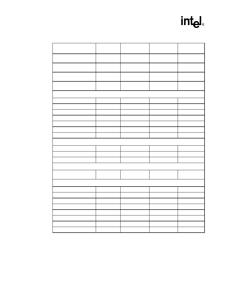
Intel
Æ
82801E C-ICH
54
Advance Information Datasheet
EE0_DOUT,
EE1_DOUT
LAN I/O
RSM_PWROK
High
Running
EE0_SHCLK,
EE1_SHCLK
LAN I/O
RSM_PWROK
Low
Running
LAN0_RSTSYNC,
LAN1_RSTSYNC
LAN I/O
RSM_PWROK
High
Defined
LAN0_TXD[2:0],
LAN1_TXD[2:0]
LAN I/O
RSM_PWROK
Low
Defined
IDE Interface
PDA[2:0], SDA[2:0]
Main I/O
PCIRST#
Low
Undefined
PDCS1#, PDCS3#
Main I/O
PCIRST#
High
High
PDD[15:0], SDD[15:0]
Main I/O
PCIRST#
High-Z
High-Z
PDDACK#, SDDACK#
Main I/O
PCIRST#
High
High
PDIOR#, PDIOW#
Main I/O
PCIRST#
High
High
SDCS1#, SDCS3#
Main I/O
PCIRST#
High
High
SDIOR#, SDIOW#
Main I/O
PCIRST#
High
High
Interrupts
PIRQ[A:H]#
Main I/O
PCIRST#
High-Z
High-Z
SERIRQ
Main I/O
PCIRST#
High-Z
High-Z
APICD[1:0]
Main I/O
PCIRST#
High-Z
High-Z
USB Interface
USBP0P, USBP0N,
USBP1P, USBP1N
Main I/O
RSMRST#
High-Z
High-Z
Processor Interface
A20M#
CPU I/O
PCIRST#
See Note 1
High
CPUPWRGD
Main I/O
PCIRST#
See Note 3
High-Z
CPUSLP#
CPU I/O
PCIRST#
High
High
IGNNE#
CPU I/O
PCIRST#
See Note 1
High
INIT#
CPU I/O
PCIRST#
High
High
INTR
CPU I/O
PCIRST#
See Note 1
Low
NMI
CPU I/O
PCIRST#
See Note 1
Low
SMI#
CPU I/O
PCIRST#
High
High
Table 32. Power Plane and States for Output and I/O Signals (Sheet 2 of 3)
Signal Name
Power Plane
Reset Signal
During Reset
Immediately
after Reset
NOTES:
1. The 82801E C-ICH sets these signals at reset for processor frequency strap.
2. I GPIO[18] will toggle at a frequency of approximately 1 Hz when the 82801E C-ICH comes out of reset
3. CPUPWRGD is an open-drain output that represents a logical AND of the VRMPWRGD and PWROK
signals and, thus, are driven low by 82801E C-ICH when either VRMPWRGD or PWROK are inactive.
During boot, or during a hard reset with power cycling, CPUPWRGD will be expected to transition from low
to High-Z.
4. GPIO[24:25, 27:28]: These signals remain tri-stated for up to 110 ms after RSMRST# deassertion. At this
point, they will be driven to their default (High) state.

Intel
Æ
82801E C-ICH
Advance Information Datasheet
55
3.4.5
Power Planes for Input Signals
Table 33 shows the power plane associated with each input signal, as well as what device drives the
signal at various times. Valid states include:
∑
High
∑
Low
∑
Static: Will be high or low, but will not change
∑
Driven: Will be high or low, and is allowed to change
∑
Running: For input clocks
STPCLK#
CPU I/O
PCIRST#
High
High
SMBus Interface
SMBCLK, SMBDATA
Main I/O
RSMRST#
High-Z
High-Z
System Management Interface
SMLINK[1:0]
Main I/O
RSMRST#
High-Z
High-Z
Miscellaneous Signals
SPKR
Main I/O
PCIRST#
High-Z with
internal pull-up
Low
SUSCLK
Main I/O
RSMRST#
Running
Unmuxed GPIO Signals
GPIO[18]
Main I/O
PCIRST#
High
See Note 2
GPIO[19:20]
Main I/O
PCIRST#
High
High
GPIO[21]
Main I/O
PCIRST#
High
High
GPIO[22]
Main I/O
PCIRST#
High-Z
High-Z
GPIO[23]
Main I/O
PCIRST#
Low
Low
GPIO[24]
Main I/O
RSMRST#
High-Z
High
GPIO[25]
Main I/O
RSMRST#
High-Z
High
GPIO[27:28]
Main I/O
RSMRST#
HIgh-Z
High
Table 32. Power Plane and States for Output and I/O Signals (Sheet 3 of 3)
Signal Name
Power Plane
Reset Signal
During Reset
Immediately
after Reset
NOTES:
1. The 82801E C-ICH sets these signals at reset for processor frequency strap.
2. I GPIO[18] will toggle at a frequency of approximately 1 Hz when the 82801E C-ICH comes out of reset
3. CPUPWRGD is an open-drain output that represents a logical AND of the VRMPWRGD and PWROK
signals and, thus, are driven low by 82801E C-ICH when either VRMPWRGD or PWROK are inactive.
During boot, or during a hard reset with power cycling, CPUPWRGD will be expected to transition from low
to High-Z.
4. GPIO[24:25, 27:28]: These signals remain tri-stated for up to 110 ms after RSMRST# deassertion. At this
point, they will be driven to their default (High) state.

Intel
Æ
82801E C-ICH
56
Advance Information Datasheet
Table 33. Power Plane for Input Signals
Signal Name
Power Well
Driver During Reset
A20GATE
Main I/O
External Microcontroller
APICCLK
Main I/O
Clock Generator
CLK14
Main I/O
Clock Generator
CLK48
Main I/O
Clock Generator
CLK66
Main Logic
Clock Generator
EE0_DIN,
EE1_DIN
LAN I/O
EEPROM component
FERR#
Main I/O
CPU
INTRUDER#
RTC
External Switch
IRQ[15:14]
Main I/O
IDE
LAN0_CLK,
LAN1_CLK
LAN I/O
LAN Connect component
RSM_PWROK
Main I/O
External RC Circuit
LAN0_RXD[2:0],
LAN1_RXD[2:0]
LAN I/O
LAN Connect component
LDRQ[0]#
Main I/O
LPC Devices
LDRQ[1]#
Main I/O
LPC Devices
OC[1:0]#
Main I/O
External Pull-Ups
PCICLK
Main I/O
Clock Generator
PDDREQ
Main I/O
IDE Device
PIORDY
Main I/O
IDE Device
PWROK
Main I/O
System Power Supply
RCIN#
Main I/O
External Microcontroller
REQ[3:0]#,
REQ[5]#
Main I/O
PCI Master
REQ[B:A]#
Main I/O
PC/PCI Devices
RI#
Main I/O
Serial Port Buffer
RSMRST#
RTC
External RC circuit
RTCRST#
RTC
External RC circuit
SDDREQ
Main I/O
IDE Drive
SERR#
Main I/O
PCI Bus Peripherals
SIORDY
Main I/O
IDE Drive
SMBALERT#
Main I/O
External pull-up
THRM#
Main I/O
Thermal Sensor
VRMPWRGD
Main I/O
CPU Voltage Regulator

Intel
Æ
82801E C-ICH
Advance Information Datasheet
57
4.0
Electrical Characteristics
Note:
This document contains information on products in the sampling and initial production phases of
development. The specifications are subject to change without notice. Verify with your local Intel
sales office that you have the latest datasheet before finalizing a design.
4.1
Absolute Maximum Ratings
Note:
A non-condensing environment is required to maintain RTC accuracy.
Warning:
Stressing the device beyond the "Absolute Maximum Ratings" may cause permanent damage.
These are stress ratings only. See Section 4.2 for the Functional Operating Range of the 82801E
C-ICH.
4.2
Functional Operating Range
All of the AC and DC Characteristics specified in this document assume that the 82801E C-ICH
component is operating within the Functional Operating Range given in this section. Operation
outside of the Functional Operating Range is not recommended, and extended exposure outside of
the Functional Operating Range may affect component reliability.
Table 34. Absolute Maximum Ratings
Case Temperature under Bias
0∫
C to +109∫
C
Storage Temperature
-55∫ C to +150∫ C
Voltage on Any 3.3 V Pin with Respect to Ground
-0.5 to Vcc + 0.3 V
Voltage on Any 5 V Tolerant Pin with Respect to Ground
(V
REF
=5 V)
-0.5 to V
REF
+ 0.3 V
1.8 V Supply Voltage with Respect to Vss
-0.5 to +2.7V
3.3 V Supply Voltage with Respect to Vss
-0.5 to +4.6 V
5.0 V Supply Voltage (Vref) with Respect to Vss
-0.5 to +5.5 V
Maximum Power Dissipation
2.0 W
Table 35. Functional Operating Range
Case Temperature under Bias
0∫ C to +109∫ C
1.8 V Supply Voltage (VCC1_8) with respect to Vss
1.7 V to 1.9 V
3.3 V Supply Voltage (VCC3_3) with respect to Vss
3.102 V to 3.498 V
5 V Supply Voltage (V5REF) with respect to Vss
4.75 V to 5.25 V
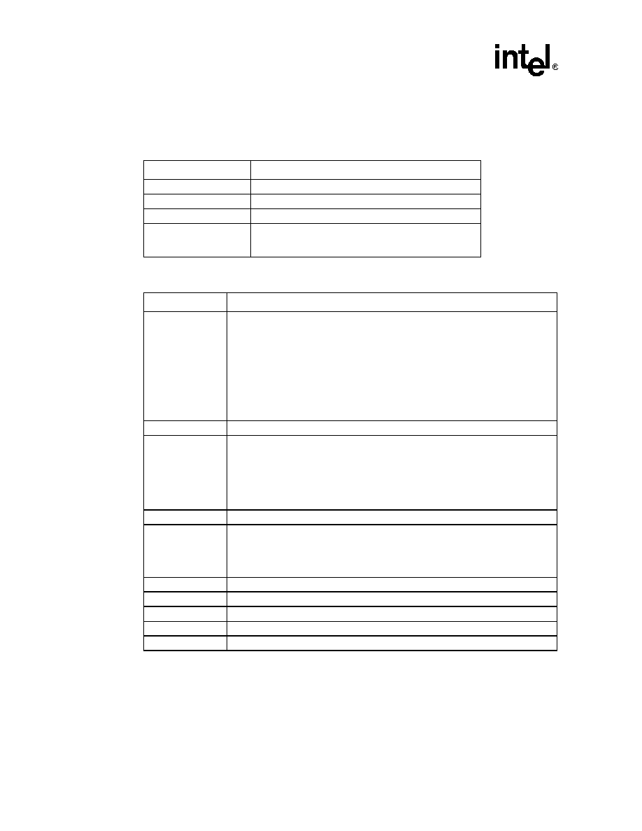
Intel
Æ
82801E C-ICH
58
Advance Information Datasheet
4.3
DC Characteristics
Table 36. 82801E C-ICH Power Consumption Measurements
Power Plane
Maximum Sustain Supply Current I
CC
(max)
1.8 V Core
300 mA
3.3 V I/O
410 mA
1.8 V LAN
30 mA
3.3 V LAN
(LAN+LAN Connect
Component)
186 mA
Table 37. DC Characteristic Input Signal Association
Symbol
Associated Signals
V
IH1
/V
IL1
(5 V Tolerant)
PCI Signals: AD[31:0], C/BE[3:0]#, DEVSEL#, FRAME#, IRDY#, TRDY#, STOP#,
PAR, PERR#, PLOCK#, SERR#, REQ[4:0]#
PC/PCI Signals: REQ[A]#/GPIO[0], REQB[#]/REQ[5]#/GPIO[1]
IDE Signals: PDD[15:0], SDD[15:0], PDDREQ, PIORDY, SDDREQ, SIORDY
Interrupt Signals: IRQ[15:14], SERIRQ, PIRQ[D:A]#, PIRQ[H]#,
PIRQ[F:G]#/GPIO[4:3], PIRQ[E]#
Legacy Signals: RCIN#, A20GATE
USB Signals: OC[1:0]#
GPIO Signals: GPIO[7:6, 4:3, 1:0]
V
IH2
/V
IL2
Clock Signals: CLK66, CLK48, CLK14, LAN_CLK, PCICLK
V
IH3
/V
IL3
LPC/FWH Signals: LDRQ[1:0]#, LAD[3:0]/FWH[3:0]
.
System Management Signals: SMBALERT#/GPIO[11]
EEPROM Signals: EE_DIN
Power Management Signals: PME#, PWRBTN#, RI#, RSM_PWROK, RTCRST#,
THRM#, VRMPWRGD
GPIO Signals: GPIO[25:24, 13:12, 8]
V
IH4
/V
IL4
Clock Signals: APICCLK
V
IH5
/V
IL5
SMBus Signals: SMBCLK, SMBDATA
System Management Signals: INTRUDER#, SMLINK[1:0]
Power Management Signals: RSMRST#, PWROK,
GPIO Signals: GPIO[28:27]
V
IL6
/V
IH6
LAN Signals: LAN0_RXD[2:0], LAN1_RXD[2:0]
V
IL7
/V
IH7
Processor Signals: FERR#, APICD[1:0]
V
IL8
/V
IH8
Hub Interface Signals: HL[11:0], HL_STB#, HL_STB
V
DI
/V
CM
/V
SE
USB Signals: USBP0P, USBP0N, USBP1P, USBP1N
V
IL9
/V
IH9
RTCX1

Intel
Æ
82801E C-ICH
Advance Information Datasheet
59
Table 38. DC Input Characteristics
Symbol
Parameter
Min.
Max
Unit
Notes
V
IL1
Input Low Voltage
-0.5
0.8
V
V
IH1
Input High Voltage
2.0
V5REF + 0.5
V
V
IL2
Input Low Voltage
-0.5
0.8
V
V
IH2
Input High Voltage
2.0
Vcc3_3 + 0.5
V
V
IL3
Input Low Voltage
-0.5
0.3Vcc3_3
V
V
IH3
Input High Voltage
0.5 Vcc3_3
Vcc3_3 + 0.5
V
V
IL4
Input Low Voltage
-0.5
0.7
V
V
IH4
Input High Voltage
1.7
2.625
V
V
IL5
Input Low Voltage
-0.5
0.6
V
V
IH5
Input High Voltage
2.1
Vcc3_3 + 0.5
V
V
IL6
Input Low Voltage
-0.5
0.3Vcc3_3
V
V
IH6
Input High Voltage
0.6 Vcc3_3
Vcc3_3 + 0.5
V
V
IL7
Input Low Voltage
-0.5
0.6
V
V
IH7
Input High Voltage
1.2
Vcc3_3 + 0.5
V
V
IL8
Input Low Voltage
-0.5
HUBREF - 0.15
V
Normal Mode
HUBREF - 0.20
Enhanced Mode
V
IH8
Input High Voltage
HUBREF + 0.15
Vcc1_8 + 0.5
V
Normal Mode
HUBREF + 0.20
Enhanced Mode
V
DI
Differential Input
Sensitivity
0.2
V
Note 1
V
CM
Differential Common
Mode Range
0.8
2.5
V
Note 2
V
SE
Single-Ended
Receiver Threshold
0.8
2.0
V
V
IL9
Input Low Voltage
-0.5
0.10
V
V
IH9
Input High Voltage
0.40
2.0
V
NOTES:
1. V
DI
= | USBPx[P] - USBPx[N] |
2. Includes V
DI
range.
Table 39. DC Characteristic Output Signal Association (Sheet 1 of 2)
Symbol
Associated Signals
V
OH1
/V
OL1
IDE Signals: PDD[15:0], SDD[15:0], PDIOW#/PDSTOP, SDIOW#/SDSTOP,
PDIOR#/PDWSTB/PRDMARDY#, SDIOR#/STWSTB/SRDMARDY#, PDDACK#,
SDDACK#, PDA[2:0], SDA[2:0], PDCS[3,1]#, SDCS[3,1]#
V
OH2
/V
OL2
Processor Signals: A20M#, CPUPWRGD, CPUSLP#, IGNNE#, INIT#, INTR, NMI,
SMI#, STPCLK#
V
OH3
/V
OL3
PCI Signals: AD[31:0], C/BE[3:0]#, PCIRST#, GNT[5, 3:0]#, PAR, DEVSEL#, PERR#,
PLOCK#, STOP#, TRDY#, IRDY#, FRAME#, SERR#
Interrupt Signals: SERIRQ, PIRQ[A:F]#, PIRQ[G:H]#/GPIO[5:4]
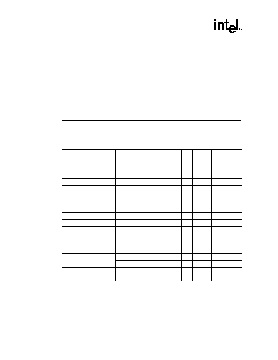
Intel
Æ
82801E C-ICH
60
Advance Information Datasheet
V
OH4
/V
OL4
PCI Signals: GNT[5]#/GNT[B]#/GPIO[17], GNT[A]#/GPIO[16]
LPC/FWH Signals: LAD[3:0]/FWH[3:0], LFRAME#/FWH[4]
LAN Signals: LAN0_RSTSYNC, LAN1_RSTSYNC, LAN0_TXD[2:0], LAN1_TXD[2:0]
GPIO Signals: GPIO[21]
V
OL5
/V
OH5
SMBus Signals: SMBCLK, SMBDATA
System Management Signals: SMLINK[1:0]
Interrupt Signals: APICD[1:0]
V
OL6
/V
OH6
EEPROM Signals: EE0_CS, EE1_CS, EE0_DOUT, EE1_DOUT, EE0_SHCLK,
EE1_SHCLK
Other Signals: SPKR
GPIO Signals: GPIO[28:27, 25:22, 20:18]
V
OL7
/V
OH7
USB Signals: USBP0P, USBP0N, USBP1P, USBP1N
V
OL8
/V
OH8
Hub Signals: HL[11:0], HL_STB#, HL_STB
Table 40. DC Output Characteristics
Symbol
Parameter
Min.
Max
Unit
I
OL /
I
OH
Notes
V
OL1
Output Low Voltage
0.5
V
4 mA
V
OH1
Output High Voltage
2.4
V
-0.4 mA
V
OL2
Output Low Voltage
0.4
V
4.0 mA
V
OH2
Output High Voltage
V_CPU_IO ≠ 0.13V
V
-0.5 mA
Note 1
V
OL3
Output Low Voltage
0.55
V
6 mA
V
OH3
Output High Voltage
2.4
V
-2 mA
Note 1
V
OL4
Output Low Voltage
0.1 Vcc
V
1.5 mA
V
OH4
Output High Voltage
0.9 Vcc
V
-0.5 mA
Note 1
V
OL5
Output Low Voltage
0.4
V
3.0 mA
V
OH5
Output High Voltage
N/A
V
Note 1
V
OL6
Output Low Voltage
0.4
V
4.0 mA
V
OH6
Output High Voltage
Vcc3_3 - 0.5
V
-2.0 mA
Note 1
V
OL7
Output Low Voltage
0.4
V
5 mA
V
OH7
Output High Voltage
Vcc - 0.5
V
-2 mA
V
OL8
Output Low Voltage
0.1
◊
(Vcc1_8)
V
1 mA
Normal Mode
0.8
V
20 mA
Enhanced Mode
V
OH8
Output High Voltage
0.9
◊
(Vcc1_8)
V
-1 mA
Normal Mode
1.6
V
-1.5 mA
Enhanced Mode
NOTES:
1. The CPUPWRGD, SERR#, PIRQ[A:H], GPIO22/CPUPERF, APIC[1:0], SMBDATA, SMBCLK and
SMLINK[1:0] signals have an open drain driver, and the VOH specification does not apply. These signals
must have external pull-up resistors.
Table 39. DC Characteristic Output Signal Association (Sheet 2 of 2)
Symbol
Associated Signals
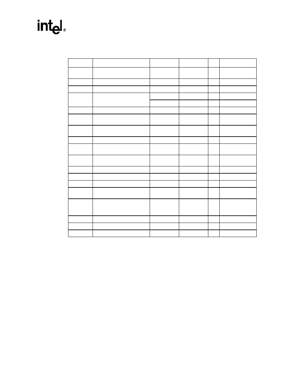
Intel
Æ
82801E C-ICH
Advance Information Datasheet
61
Table 41. Other DC Characteristics
Symbol
Parameter
Min.
Max
Unit
Notes
V5REF
ICH2 Core Well Reference
Voltage
4.75
5.25
V
VCC3_3
I/O Buffer Voltage
3.102
3.498
V
VCC1_8
Internal Logic Voltage
1.7
1.9
V
HUBREF
Hub Interface Reference
Voltage
0.48
◊
(Vcc1.8)
0.52
◊
(Vcc1.8)
V
Normal Mode
0.64
◊
(Vcc1.8)
0.70
◊
(Vcc1.8)
V
Enhanced Mode
Vcc(RTC)
Battery Voltage
2.0
3.6
V
VIT+
Hysteresis Input Rising
Threshold
1.9
V
Applied to
USBP[1:0][P:N]
VIT-
Hysteresis Input Falling
Threshold
1.3
V
Applied to
USBP[1:0]P:N]
VDI
Differential Input Sensitivity
0.2
V
|(USBPx+,USBPx-)|
VCM
Differential Common Mode
Range
0.8
2.5
V
Includes VDI
VCRS
Output Signal Crossover
Voltage
1.3
2.0
V
VSE
Single Ended Rcvr Threshold
0.8
2.0
V
ILI1
Input Leakage Current
-1.0
+1.0
µA
ILI2
Hi-Z State Data Line Leakage
-10
+10
µA
(0 V< VIN< 3.3V)
ILI3
Input Leakage Current - Clock
signals
-100
+100
µA
See Note
CIN
Input Capacitance - Hub
interface
Input Capacitance - All Other
8
12
pF
FC = 1 MHz
COUT
Output Capacitance
12
pF
FC = 1 MHz
CI/O
I/O Capacitance
12
pF
FC = 1 MHz
CL
Crystal Load Capacitance
pF
2.5 ≠ 6 pF Typical
NOTES:
1. Includes APICCLK, CLK14, CLK48, CLK66, LAN_CLK and PCICLK

Intel
Æ
82801E C-ICH
62
Advance Information Datasheet
4.4
AC Characteristics
Table 42. Clock Timings (Sheet 1 of 2)
Sym
Parameter
Min
Max
Unit
Notes
Figure
PCI Clock (PCICLK)
t1
Period
30
33.3
ns
9
t2
High Time
12
ns
9
t3
Low Time
12
ns
9
t4
Rise Time
3
ns
9
t5
Fall Time
3
ns
9
Oscillator Clock (OSC)
t6
Period
67
70
ns
9
t7
High Time
20
9
t8
Low time
20
ns
9
USB Clock (USBCLK)
fclk48
Operating Frequency
48
MHz
t9
Frequency Tolerance
500
ppm
1
t10
High Time
7
ns
9
t11
Low time
7
ns
9
t12
Rise Time
1.2
ns
9
t13
Fall Time
1.2
ns
9
Suspend Clock (SUSCLK)
fsusclk
Operating Frequency
32
KHz
4
t14
High time
10
µs
4
9
t15
Low Time
10
µs
4
9
SMBus Clock (SMBCLK)
fsmb
Operating Frequency
10
16
KHz
t18
High time
4.0
50
µs
2
24
t19
Low time
4.7
µs
24
t20
Rise time
1000
ns
24
t21
Fall time
300
ns
24
I/O APIC Clock (APICCLK)
fioap
Operating Frequency
14.32
33.33
MHz
NOTES:
1. The USBCLK is a 48 MHz that expects a 40/60% duty cycle. The source of this PPM is external to this
component.
2. The maximum high time (t18 Max) provide a simple guaranteed method for devices to detect bus idle
conditions.
3. This specification includes pin-to-pin skew from the clock generator as well as board skew.
4. SUSCLK duty cycle can range from 30% minimum to 70% maximum.

Intel
Æ
82801E C-ICH
Advance Information Datasheet
63
t22
High time
12
36
ns
9
t23
Low time
12
36
ns
9
t24
Rise time
1.0
5.0
ns
9
t25
Fall time
1.0
5.0
ns
9
Hub Interface Clock
fhl
Operating Frequency
66
t31
High time
6.0
ns
9
t32
Low time
6.0
ns
9
t33
Rise time
0.25
1.2
ns
9
t34
Fall time
0.25
1.2
ns
9
t35
CLK66 leads PCICLK
1.0
4.5
3
Table 43. Clock Timings - UART_CLK
Sym
Parameter
Min
Max
Units
Notes
Fig
t1a
Operating Frequency
14.7456
48
MHz
t9a
Frequency Tolerance
2500
PPM
t10a
High Time
7
ns
9
t11a
Low time
7
ns
9
t12a
Rise Time
3
ns
9
t155a
Fall Time
3
ns
9
Table 44. PCI Interface Timing (Sheet 1 of 2)
Sym
Parameter
Min
Max
Units
Notes
Figure
t40
AD[31:0] Valid Delay
2
11
ns
Min: 0pF
Max: 50pF
10
t41
AD[31:0] Setup Time to PCICLK Rising
7
ns
11
t42
AD[31:0] Hold Time from PCICLK Rising
0
ns
11
t43
C/BE[3:0]#, FRAME#, TRDY#, IRDY#, STOP#,
PAR, PERR#, PLOCK#, DEVSEL# Valid Delay
from PCICLK Rising
2
11
ns
Min: 0pF
Max: 50pF
10
t44
C/BE[3:0]#, FRAME#, TRDY#, IRDY#, STOP#,
PAR, PERR#, PLOCK#, IDSEL, DEVSEL# Output
Enable Delay from PCICLK Rising
2
ns
14
Table 42. Clock Timings (Sheet 2 of 2)
Sym
Parameter
Min
Max
Unit
Notes
Figure
NOTES:
1. The USBCLK is a 48 MHz that expects a 40/60% duty cycle. The source of this PPM is external to this
component.
2. The maximum high time (t18 Max) provide a simple guaranteed method for devices to detect bus idle
conditions.
3. This specification includes pin-to-pin skew from the clock generator as well as board skew.
4. SUSCLK duty cycle can range from 30% minimum to 70% maximum.

Intel
Æ
82801E C-ICH
64
Advance Information Datasheet
t45
C/BE[3:0]#, FRAME#, TRDY#, IRDY#, STOP#,
PERR#, PLOCK#, DEVSEL#, GNT[A:B]# Float
Delay from PCICLK Rising
2
28
ns
12
t46
C/BE[3:0]#, FRAME#, TRDY#, IRDY#, STOP#,
SERR#, PERR#, DEVSEL#, Setup Time to
PCICLK Rising
7
ns
11
t47
C/BE[3:0]#, FRAME#, TRDY#, IRDY#, STOP#,
SERR#, PERR#, DEVSEL#, REQ[A:B]# Hold
Time from PCLKIN Rising
0
ns
11
t48
PCIRST# Low Pulse Width
1
ms
13
t49
GNT[A:B}#, GNT[5, 3:0]# Valid Delay from
PCICLK Rising
2
12
ns
t50
REQ[A:B]#, REQ[5, 3:0]# Setup Timer to PCICLK
Rising
12
ns
Table 45. IDE PIO & Multiword DMA Mode Timing (Sheet 1 of 2)
Sym
Parameter
Min
Max
Units
Notes
Figure
t60
PDIOR#/PDIOW#/SDIOR#/SDIOW# Active From
CLK66 Rising
2
20
ns
15, 16
t61
PDIOR#/PDIOW#/SDIOR#/SDIOW# Inactive From
CLK66 Rising
2
20
ns
15, 16
t62
PDA[2:0]/SDA[2:0] Valid Delay From CLK66 Rising
2
30
ns
15
t63
PDCS1#/SDCS1#, PDCS3#/SDCS3# Active From
CLK66 Rising
2
30
ns
15
t64
PDCS1#/SDCS1#, PDCS3#/SDCS3# Inactive From
CLK66 Rising
2
30
ns
15
t65
PDDACK#/SDDACK# Active From CLK66 Rising
2
20
ns
16
t66
PDDACK#/SDDACK# Inactive From CLK66 Rising
2
20
ns
t67
PDDREQ/SDDREQ Setup Time to CLK66 Rising
7
ns
16
t68
PDDREQ/SDDREQ Hold From CLK66 Rising
7
ns
16
t69
PDD[15:0]/SDD[15:0] Valid Delay From CLK66
Rising
2
30
ns
15, 16
t70
PDD[15:0]/SDD[15:0] Setup Time to CLK66 Rising
10
ns
15, 16
t71
PDD[15:0]/SDD[15:0] Hold From CLK66 Rising
7
ns
15, 16
t72
PIORDY/SIORDY Setup Time to CLK66 Rising
7
ns
1
15
t73
PIORDY/SIORDY Hold From CLK66 Rising
7
ns
1
15
NOTES:
1. IORDY is internally synchronized. This timing is to guarantee recognition on the next clock.
2. PIORDY sample point from DIOx# assertion and PDIOx# active pulse width is programmable from 2-5 PCI
clocks when the drive mode is Mode 2 or greater. Refer to the ISP field in the IDE Timing Register
3. PIORDY sample point from DIOx# assertion, PDIOx# active pulse width and PDIOx# inactive pulse width
cycle time is the compatible timing when the drive mode is Mode 0/1. Refer to the TIM0/1 field in the IDE
timing register.
4. PDIOx# inactive pulse width is programmable from 1-4 PCI clocks when the drive mode is Mode 2 or
greater. Refer to the RCT field in the IDE Timing Register.
Table 44. PCI Interface Timing (Sheet 2 of 2)
Sym
Parameter
Min
Max
Units
Notes
Figure
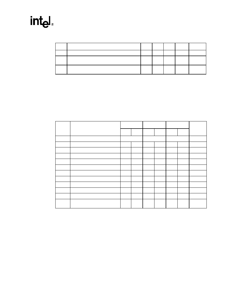
Intel
Æ
82801E C-ICH
Advance Information Datasheet
65
t74
PIORDY/SIORDY Inactive Pulse Width
48
ns
15
t75
PDIOR#/PDIOW#/SDIOR#/SDIOW# Pulse Width
Low
2,3
15, 16
t76
PDIOR#/PDIOW#/SDIOR#/SDIOW# Pulse Width
High
3,4
15, 16
Table 46. Ultra ATA Timing (Mode 0, Mode 1, Mode 2)
Sym
Parameter (1)
Mode 0 (ns)
Mode 1 (ns)
Mode 2 (ns)
Figure
Min
Max
Min
Max
Min
Max
t80
Sustained Cycle Time (T2cyctyp)
240
160
120
t81
Cycle Time (Tcyc)
112
73
54
18
t82
Two Cycle Time (T2cyc)
230
154
115
18
t83
Data Setup Time (Tds)
15
10
7
18
t84
Data Hold Time (Tdh)
5
5
5
18
t85
Data Valid Setup Time (Tdvs)
70
48
30
18
t86
Data Valid Hold Time (Tdvh)
6
6
6
18
t87
Limited Interlock Time (Tli)
0
150
0
150
0
150
20
t88
Interlock Time w/ Minimum (Tmli)
20
20
20
20
t89
Envelope Time (Tenv)
20
70
20
70
20
70
17
t90
Ready to Pause Time (Trp)
160
125
100
19
t91
DMACK setup/hold Time (Tack)
20
20
20
17,
20
NOTE:
1. The specification symbols in parentheses correspond to the Ultra ATA specification name.
Table 45. IDE PIO & Multiword DMA Mode Timing (Sheet 2 of 2)
Sym
Parameter
Min
Max
Units
Notes
Figure
NOTES:
1. IORDY is internally synchronized. This timing is to guarantee recognition on the next clock.
2. PIORDY sample point from DIOx# assertion and PDIOx# active pulse width is programmable from 2-5 PCI
clocks when the drive mode is Mode 2 or greater. Refer to the ISP field in the IDE Timing Register
3. PIORDY sample point from DIOx# assertion, PDIOx# active pulse width and PDIOx# inactive pulse width
cycle time is the compatible timing when the drive mode is Mode 0/1. Refer to the TIM0/1 field in the IDE
timing register.
4. PDIOx# inactive pulse width is programmable from 1-4 PCI clocks when the drive mode is Mode 2 or
greater. Refer to the RCT field in the IDE Timing Register.

Intel
Æ
82801E C-ICH
66
Advance Information Datasheet
Table 47. Ultra ATA Timing (Mode 3, Mode 4, Mode 5)
Sym
Parameter (1)
Mode 3 (ns)
Mode 4 (ns)
Mode 5 (ns)
Figure
Min
Max
Min
Max
Min
Max
t80
Sustained Cycle Time (T2cyctyp)
90
60
40
t81
Cycle Time (Tcyc) (2)
39
25
16.8
18
t82
Two Cycle Time (T2cyc)
86
57
38
18
t83
Data Setup Time (Tds)
7
5
4.0
18
t84
Data Hold Time (Tdh)
5
5
4.6
18
t85
Data Valid Setup Time (Tdvs)
20
6
6.0
18
t86
Data Valid Hold Time (Tdvh)
6
6
6.0
18
t87
Limited Interlock Time (Tli)
0
100
0
100
0
75
20
t88
Interlock Time w/ Minimum (Tmli)
20
20
20
20
t89
Envelope Time (Tenv)
20
55
20
55
20
50
17
t90
Ready to Pause Time (Trp)
100
100
85
19
t91
DMACK setup/hold Time (Tack)
20
20
20
17,
20

Intel
Æ
82801E C-ICH
Advance Information Datasheet
67
Table 48. Universal Serial Bus Timing
Sym
Parameter
Min
Max
Units
Notes
Fig
Full Speed Source (Note 7)
t122
USBPx+, USBPx- Driver Rise Time
4
20
ns
1, CL = 50 pF
21
t123
USBPx+, USBPx- Driver Fall Time
4
20
ns
1, CL = 50 pF
21
t102
Source Differential Driver Jitter
To Next Transition
For Paired Transitions
-3.5
-4
3.5
4
ns
ns
2, 3
22
t103
Source SE0 interval of EOP
160
175
ns
4
23
t104
Source Jitter for Differential Transition to
SE0 Transition
-2
5
ns
5
t105
Receiver Data Jitter Tolerance
To Next Transition
For Paired Transitions
-18.5
-9
18.5
9
ns
ns
3
22
t106
EOP Width: Must accept as EOP
82
ns
4
23
t107
Width of SE0 interval during differential
transition
14
ns
Low Speed Source (Note 8)
t122
USBPx+, USBPx- Driver Rise Time
75
300
ns
ns
1, 6
CL = 50 pF
CL = 350 pF
21
t123
USBPx+, USBPx- Driver Fall Time
75
300
ns
ns
1,6
CL = 50 pF
CL = 350 pF
21
t110
Source Differential Driver Jitter
To Next Transition
For Paired Transitions
-25
-14
25
14
ns
ns
2, 3
22
t111
Source SE0 interval of EOP
1.25
1.50
µs
4
23
t112
Source Jitter for Differential Transition to
SE0 Transition
-40
100
ns
5
t113
Receiver Data Jitter Tolerance
To Next Transition
For Paired Transitions
-152
-200
152
200
ns
ns
3
22
t114
EOP Width: Must accept as EOP
670
ns
4
23
t115
Width of SE0 Interval during Differential
Transition
210
ns
5
NOTES:
1. Driver output resistance under steady state drive is specified at 28 ohms at minimum and 43 ohms at
maximum
2. Timing difference between the differential data signals
3. Measured at crossover point of differential data signals
4. Measured at 50% swing point of data signals
5. Measured from last crossover point to 50% swing point of data line at leading edge of EOP
6. Measured from 10% to 90% of the data signal
7. Full Speed Data Rate has minimum of 11.97 Mbps and maximum of 12.03 Mbps
8. Low Speed Data Rate has a minimum of 1.48 Mbps and a maximum of 1.52 Mbps

Intel
Æ
82801E C-ICH
68
Advance Information Datasheet
Table 49. IOAPIC Bus Timing
Sym
Parameter
Min
Max
Units
Notes
Fig
t120
APICCD[1:0]# Valid Delay from APICCLK Rising
3.0
12.0
ns
10
t121
APICCD[1:0]# Setup Time to APICCLK Rising
8.5
ns
11
t122
APICCD[1:0]# Hold Time from APICCLK Rising
3.0
ns
11
Table 50. SMBus Timing
Sym
Parameter
Min
Max
Units
Notes
Fig
t130
Bus Tree Time Between Stop and Start Condition
4.7
µs
24
t131
Hold Time after (repeated) Start Condition. After this
period, the first clock is generated.
4.0
µs
24
t132
Repeated Start Condition Setup Time
4.7
µs
24
t133
Stop Condition Setup Time
4.0
µs
24
t134
Data Hold Time
300
ns
24
t135
Data Setup Time
250
ns
24
t136
Device Time Out
25
35
ms
1
t137
Cumulative Clock Low Extend Time (slave device)
25
ms
2
25
t138
Cumulative Clock Low Extend Time (master device)
10
ms
3
25
NOTES:
1. A device will time out when any clock low exceeds this value.
2. t137 is the cumulative time a slave device is allowed to extend the clock cycles in one message from the
initial start to stop. If a slave device exceeds this time, it is expected to release both its clock and data lines
and reset itself.
3. t138 is the cumulative time a master device is allowed to extend its clock cycles within each byte of a
message as defined from start-to-ack, ack-to-ack or ack-to-stop.
Table 51. SIU LPC and Serial IRQ Timings
Sym
Parameter
Min
Max
Units
Notes
Fig
t150a
SIU_LAD[3:0]/SIU_SERIRQ Valid Delay from
SIU_LCLK Rising
2
11
ns
10
t151a
SIU_LAD[3:0]/SIU_SERIRQ Output Enable Delay from
SIU_LCLK Rising
2
ns
14
t152a
SIU_LAD[3:0]/SIU_SERIRQ Float Delay from
SIU_LCLK Rising
28
ns
12
t153a
SIU_LAD[3:0]/SIU_SERIRQ Setup Time to SIU_LCLK
Rising
7
ns
11
t154a
SIU_LAD[3:0]/SIU_SERIRQ Hold Time from SIU_LCLK
Rising
0
ns
11
t155a
SIU_LDRQ# Valid Delay from SIU_LCLK Rising
2
11
ns
10
t157a
SIU_LFRAME# Setup Time to SIU_LCLK Rising
7
ns
11
t157b
SIU_LAD[3:0] Hold Time from SIU_LCLK Rising
0
ns
11
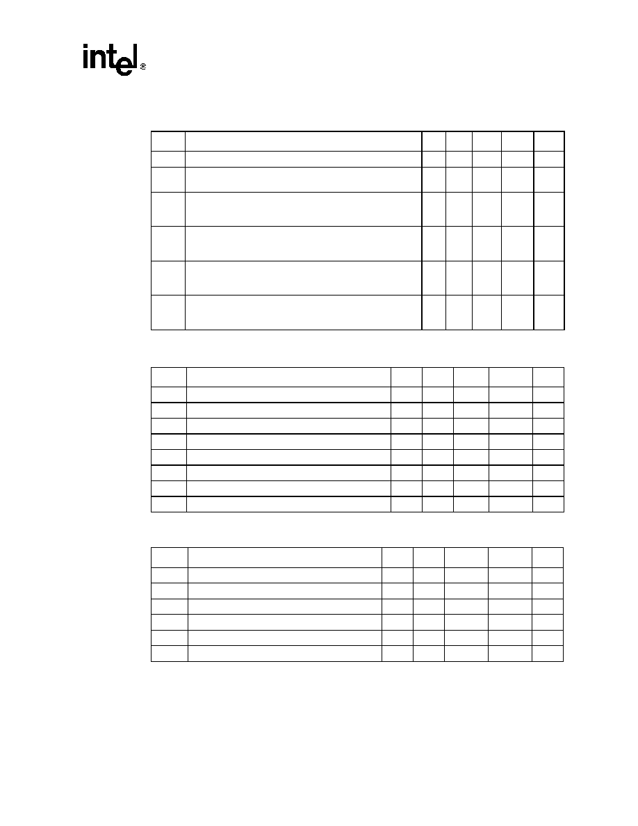
Intel
Æ
82801E C-ICH
Advance Information Datasheet
69
Table 52. UART Timings
Sym
Parameter
Min
Max
Units
Notes
Fig
t150a
SIU0_TXD, SIU1_TXD Valid Delay from UART_CLK Rising
2
13
ns
10
t150a
SIU0_DTR#, SIU0_RTS#, SIU1_DTR#, and SIU1_RTS# Valid
Delay from SIU_LCLK Rising
2
11
ns
10
t153a
SIU0_RXD, SIU0_CTS#, SIU0_DSR#, SIU0_DCD#,
SIU0_RI# SIU1_RXD, SIU1_CTS#, SIU1_DSR#,
SIU1_DCD#, and SIU1_RI# Setup Time to SIU_LCLK Rising
7
ns
11
t154a
SIU0_RXD, SIU0_CTS#, SIU0_DSR#, SIU0_DCD#,
SIU0_RI#, SIU1_RXD, SIU1_CTS#, SIU1_DSR#,
SIU1_DCD#, and SIU1_RI# Hold Time from SIU_LCLK Rising
0
ns
11
t10a
SIU0_CTS#, SIU0_DSR#, SIU0_DCD#, SIU0_RI#,
SIU1_CTS#, SIU1_DSR#, SIU1_DCD#, and SIU1_RI#
high time
100
9
t11a
SIU0_CTS#, SIU0_DSR#, SIU0_DCD#, SIU0_RI#,
SIU1_CTS#, SIU1_DSR#, SIU1_DCD#, and SIU1_RI#
low time
100
9
Table 53. LPC Timing
Sym
Parameter
Min
Max
Units
Notes
Fig
t150
LAD[3:0] Valid Delay from PCICLK Rising
2
11
ns
10
t151
LAD[3:0] Output Enable Delay from PCICLK Rising
2
ns
14
t152
LAD[3:0] Float Delay from PCICLK Rising
28
ns
12
t153
LAD[3:0] Setup Time to PCICLK Rising
7
ns
11
t154
LAD[3:0] Hold Time from PCICLK Rising
0
ns
11
t155
LDRQ[1:0]# Setup Time to PCICLK Rising
12
ns
11
t156
LDRQ[1:0]# Hold Time from PCICLK Rising
0
ns
11
t157
LFRAME# Valid Delay from PCICLK Rising
2
12
ns
10
Table 54. Miscellaneous Timings
Sym
Parameter
Min
Max
Units
Notes
Fig
t160
SERIRQ Setup Time to PCICLK Rising
7
ns
11
t161
SERIRQ Hold Time from PCICLK Rising
0
ns
11
t162
RI#, EXTSMI#, GPI, USB Resume Pulse Width
2
RTCCLK
13
t163
SPKR Valid Delay from OSC Rising
200
ns
10
t164
SERR# Active to NMI Active
200
ns
t165
IGNNE# Inactive from FERR# Inactive
230
ns

Intel
Æ
82801E C-ICH
70
Advance Information Datasheet
4.5
Timing Diagrams
Table 55. Power Sequencing and Reset Signal Timings
Sym
Parameter
Min
Max
Units
Notes
Fig
t170
VccRTC active to RTCRST# inactive
5
-
ms
26
t171
VccRTC supply active to Vcc supplies active
0
-
ms
3
26
t172
V5Ref active to Vcc3_3, Vcc1_8 active
0
-
ms
1, 2
26, 27
t173
Vcc supplies active to PWROK, VRMPWRGD
active
10
-
ms
2
26, 27
t174
AC_RST# active low pulse width
1
µs
t175
AC_RST# inactive to BIT_CLK startup delay
162.8
ns
NOTES:
1. The V5Ref supply must power up before or simultaneous with its associated 3.3 V supply, and must power
down simultaneous with or after the 3.3V supply. See Section 3.3.4 for details.
2. The associated 3.3 V and 1.8 V supplies are assumed to power up or down together. The difference
between the levels of the 3.3 V and 1.8 V supplies must never be greater than 2.0V.
3. The Vcc supplies must never be active while the VccRTC supply is inactive.
Figure 9. Clock Timing
Figure 10. Valid Delay From Rising Clock Edge
2.0V
0.8V
Period
High Time
Low Time
Fall Time
Rise Time
Clock
1.5V
Valid Delay
VT
Output

Intel
Æ
82801E C-ICH
Advance Information Datasheet
71
Figure 11. Setup And Hold Times
Figure 12. Float Delay
Figure 13. Pulse Width
Figure 14. Output Enable Delay
Clock
VT
Input
Hold Time
Setup Time
VT
1.5V
Input
VT
Output
Float
Delay
VT
Pulse Width
VT
Clock
Output
Output
Enable
Delay
VT
1.5V
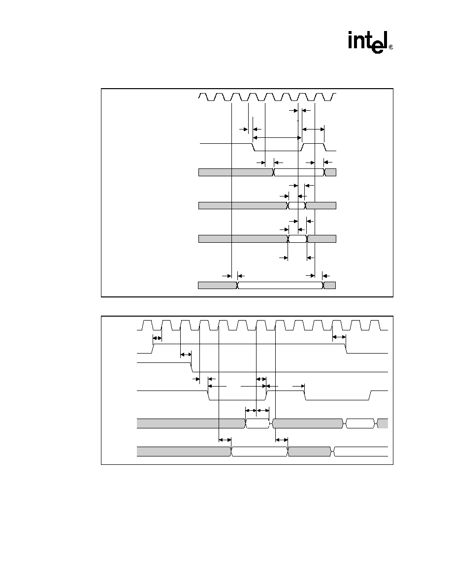
Intel
Æ
82801E C-ICH
72
Advance Information Datasheet
Figure 15. IDE PIO Mode
Figure 16. IDE Multiword DMA
t62,t63
t64
DA[2:0], CS1#, CS3#
t75
t69
t69
t70
t71
t72
t73
t61
read data
CLK66
DIOx#
DD[15:0] Write
DD[15:0] Read
IORDY
t60
t76
write data
sample point
t74
CLK66
id d
d
t67
DDREQ[1:0]
DDACK[1:0]
t65
DIOx#
DD[15:0] Read
DD[15:0] Write
t60
t61
t75
t76
t70
t71
t69
t69
Read Data
Write Data
Write Data
Read Data
t68
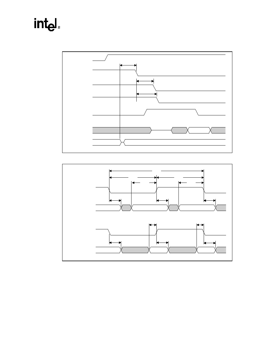
Intel
Æ
82801E C-ICH
Advance Information Datasheet
73
Figure 17. Ultra ATA Mode (Drive Initiating a Burst Read)
Figure 18. Ultra ATA Mode (Sustained Burst)
DMARQ (drive)
t91
t89
t89
DMACK# (host)
STOP (host)
DMARDY# (host)
STROBE (drive)
DD[15:0]
DA[2:0], CS[1:0]
STROBE @ sender
t81
Data @ sender
t86
t85
t86
t85
t81
t82
t86
STROBE @ receiver
Data @ receiver
t84
t83
t84
t83
t84
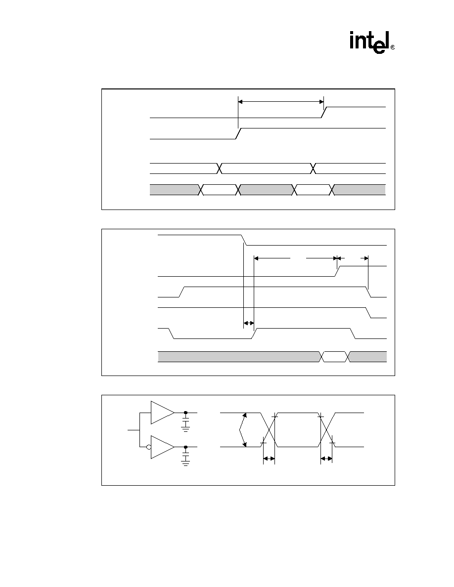
Intel
Æ
82801E C-ICH
74
Advance Information Datasheet
Figure 19. Ultra ATA Mode (Pausing a DMA Burst)
Figure 20. Ultra ATA Mode (Terminating a DMA Burst)
Figure 21. USB Rise and Fall Times
t90
STROBE
DATA
STOP (host)
DMARDY#
t88
STOP (host)
Strobe (host)
DMARDY# (drive)
DATA (host)
DMACK# (host)
t91
t87
DMARQ (drive)
CRC
Full Speed: 4 to 20 ns at C
L
= 50 pF
Differential
Data Lines
90%
10%
10%
90%
t122
t123
Rise Time
Fall Time
Low Speed: 75 ns at C
L
= 50 pF, 300 ns at C
L
= 350 pF
C
L
C
L

Intel
Æ
82801E C-ICH
Advance Information Datasheet
75
Figure 22. USB Jitter
Figure 23. USB EOP Width
Figure 24. SMBus Transaction
Figure 25. SMBus Time-out
Differential
Data Lines
Consecutive
Transitions
Paired
Transitions
Crossover
Points
Tperiod
Differential
Data Lines
EOP
Width
Data
Crossover
Level
Tperiod
t130
SMBCLK
SMBDATA
t131
t19
t134
t20
t21
t135
t132
t18
t133
Start
Stop
t137
CLK
ack
CLK
ack
t138
t138
SMBCLK
SMBDATA
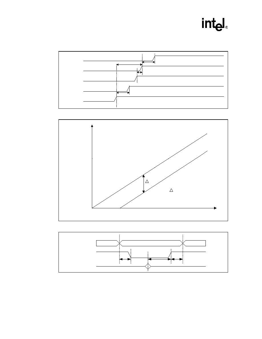
Intel
Æ
82801E C-ICH
76
Advance Information Datasheet
Figure 26. Power Sequencing and Reset Signal Timings
Figure 27. 1.8 V/3.3 V Power Sequencing
Figure 28. C0 to C2 to C0 Timings
VccRTC
V5Ref
Vcc3_3, Vcc1_8,
V_CPU_IO
RTCRST#
PWROK,
VRMPWRGD
T170
T172
T171
T173
ich2_powerup_reset_DT.vsd
t
Time
1.8
3.3
V
V
V < 2.0V
Voltage
S
2
Unlatched
Latched
Unlatched
CPU I/F
Signals
STPCLK#
Break
Event
ICH2 C0 C2 Ti i
d
T204
T205
T206
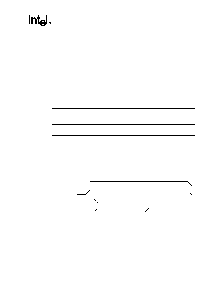
Intel
Æ
82801E C-ICH
Advance Information Datasheet
77
5.0
Testability
5.1
Test Mode Description
The 82801E C-ICH supports two types of test modes, a tri-state test mode and an XOR Chain test
mode. Driving RTCRST# low for a specific number of PCI clocks while PWROK is high activates
a particular test mode as described in Table 56.
Note:
RTCRST# can be driven low any time after PCIRST# is inactive.
.
Figure 29 illustrates the entry into a test mode. A particular test mode is entered upon the rising
edge of the RTCRST# after being asserted for a specific number of PCI clocks while PWROK is
active. To change test modes, the same sequence should be followed again. To restore the 82801E
C-ICH to normal operation, execute the sequence with RTCRST# being asserted so that no test
mode is selected as specified in Table 56.
Table 56. Test Mode Selection
Number of PCI Clocks RTCRST# Driven Low After
PWROK Active
Test Mode
<4
No Test Mode Selected
4
XOR Chain 1
5
XOR Chain 2
6
XOR Chain 3
7
XOR Chain 4
8
All "Z"
9 - 24
Reserved. DO NOT ATTEMPT
>24
No Test Mode Selected
Figure 29. Test Mode Entry (XOR Chain Example)
RSMRST#
PWROK
RTCRST#
Other Signal
Outputs
N Number of PCI Clocks
Test Mode Entered
All Output Signals Tri-Stated
XOR Chain Output Enabled

Intel
Æ
82801E C-ICH
78
Advance Information Datasheet
5.2
Tri-state Mode
When in the tri-state mode, all outputs and bidirectional pin are tri-stated, including the XOR
Chain outputs.
5.3
XOR Chain Mode
In the 82801E C-ICH, provisions for Automated Test Equipment (ATE) board level testing are
implemented with XOR Chains. The 82801E C-ICH signals are grouped into four independent
XOR chains which are enabled individually. When an XOR chain is enabled, all output and
bidirectional buffers within that chain are tri-stated, except for the XOR chain output. Every signal
in the enabled XOR chain (except for the XOR chain's output) functions as an input. All output and
bidirectional buffers for pins not in the selected XOR chain are tri-stated. Figure 30 is a schematic
example of XOR chain circuitry.
Table 57 - Table 60 list each XOR chain pin ordering, with the first value being the first input and
the last value being the XOR chain output. Table 61 lists the signal pins not included in any XOR
chain.
Figure 30. Example XOR Chain Circuitry
Input
Pin 2
Vcc
Input
Pin 1
Input
Pin 3
Input
Pin 4
Input
Pin 5
Input
Pin 6
XOR
Chain
Output
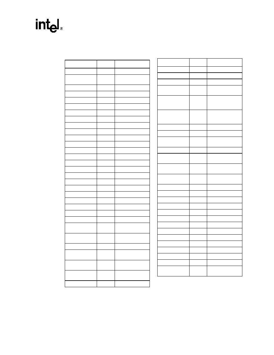
Intel
Æ
82801E C-ICH
Advance Information Datasheet
79
Table 57. XOR Chain #1
(RTCRST# Asserted for four PCI Clocks while
PWROK Active)
Pin Name
Ball #
Notes
SIU0_RXD
E17
Top of XOR Chain 1
SIU0_TXD
D19
Second signal in
XOR
SIU0_CTS#
D17
SIU0_DSR#
D18
SIU0_DCD#
B20
SIU0_RI#
A21
SIU0_DTR#
B19
SIU0_RTS#
E16
SIU1_RXD
B18
SIU1_TXD
C17
SIU1_CTS#
D16
SIU1_DSR#
A18
SIU1_DCD#
C16
SIU1_RI#
D15
SIU1_DTR#
B16
SIU1_RTS#
A16
SIU_LDRQ#
C15
SIU_LAD[3]
E14
SIU_LFRAME#
B15
SIU_LAD[0]
D14
SIU_LAD[1]
A15
SIU_LAD[2]
C14
SIU_SERIRQ
A14
SIU_RESET#
D13
LFRAME#
/FWH4
C13
FWH3
/LAD3
B13
TP0
A12
FWH0
/LAD0
B12
FWH1
/LAD1
D12
FWH2
/LAD2
E12
THRM#
A11
LDRQ0#
B11
LDRQ1#
C11
GPIO[21]
A10
GNTA#
/GPIO16
B10
REQB#
/REQ5#
/GPIO1
C10
GNTB#
/GNT5#
/GPIO17
B9
GNT1#
D10
GNT0#
A8
REQA#
/GPIO0
C9
PIRQH#
A7
PIRQG#
/GPIO4
E11
PIRQF#
/GPIO3
E10
PIRQE#
/GPIO2
C8
PIRQD#
B7
PIRQA#
A5
PIRQB#
D8
PIRQC#
C7
REQ0#
B5
REQ1#
D7
REQ2#
E9
GNT2#
E8
GNT3#
A3
AD_26
B4
AD_30
C5
AD_24
D6
AD_28
A2
TP[2]
AC2
XOR Chain #1
Output
Table 57. XOR Chain #1
(RTCRST# Asserted for four PCI Clocks while
PWROK Active)
Pin Name
Ball #
Notes
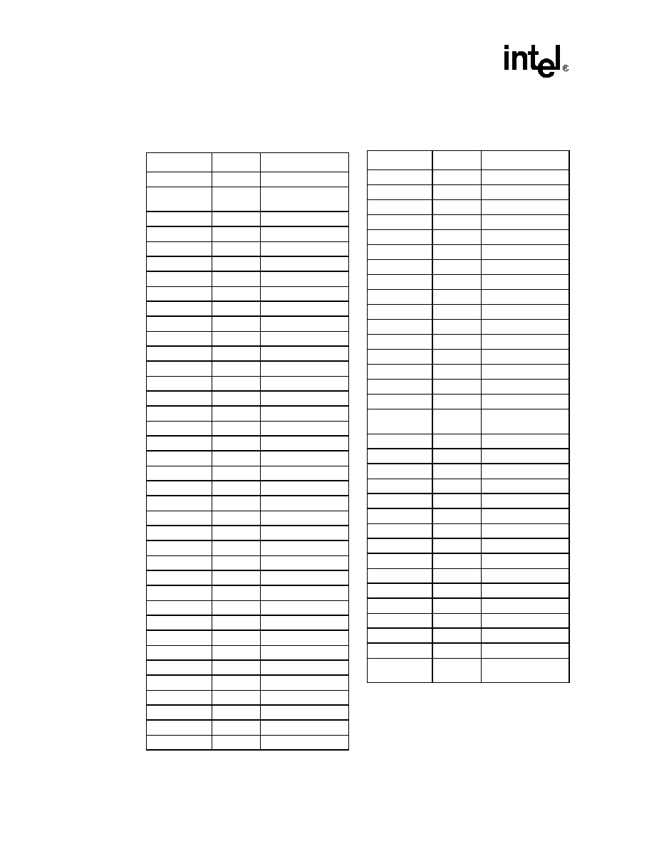
Intel
Æ
82801E C-ICH
80
Advance Information Datasheet
Table 58. XOR Chain #2; Chain 2-1 and
Chain 2-2
(RTCRST# Asserted for Five PCI Clocks while
PWROK Active)
Pin Name
Ball #
Notes
AD_18
D5
Top of XOR Chain 2
AD_22
B3
Second signal in
XOR
AD_16
B2
STOP#
D4
PAR
C3
FRAME#
B1
AD_20
C2
AD_15
D3
TRDY#
E4
AD_11
F5
AD_13
C1
AD_4
D2
AD_9
E3
C/BE[0]#
F4
AD_2
G5
AD_6
F3
AD_3
G4
AD_0
E1
AD_5
H5
AD_10
F2
AD_7
F1
AD_1
H4
AD_12
G2
AD_8
H3
SERR#
G1
AD_14
H2
PERR#
J4
C/BE[1]#
H1
DEVSEL#
J3
PLOCK#
K5
C/BE[2]#
J2
IRDY#
K4
AD_17
K3
AD_19
K2
AD_23
K1
AD_21
L5
C/BE[3]#
L4
AD_25
L2
AD_27
L1
AD_29
M1
AD_31
M2
REQ3#
M4
GPIO[6]
M3
GPIO[7]
N2
Out XOR Chain 2-1
GPIO[27]
N3
In XOR Chain 2-2
GPIO[28]
N4
GPIO[8]
P1
GPIO[12]
P2
GPIO[13]
P3
PCIRST#
R1
RESERVED1
P4
GPIO[25]
R2
SMBCLK
T2
SMBDATA
R4
SMBALERT#
/GPIO11
U1
NC[11]
U2
NC[12]
T4
NC[10]
V1
SUSCLK
U3
USBP0P
U4
USBP0N
T5
USBP1P
W1
USBP1N
V2
NC[9]
W2
NC[6]
V4
NC[7]
W3
NC[8]
Y2
OC1#
W4
VSS
AB2
RESERVED2
Y4
TP[1]
AA5
XOR Chain #2
Output, (Chain 2-2)
Table 58. XOR Chain #2; Chain 2-1 and
Chain 2-2
(RTCRST# Asserted for Five PCI Clocks while
PWROK Active)
Pin Name
Ball #
Notes

Intel
Æ
82801E C-ICH
Advance Information Datasheet
81
Table 59. XOR Chain #3; Chain 3-1 and
Chain 3-2
(RTCRST# Asserted for Six PCI Clocks While
PWROK Active)
Pin Name
Ball #
Notes
SMLINK1
AA4
Top of XOR Chain 3
SMLINK0
Y5
Second signal in XOR
NC
W7
GPIO[24]
AB4
Out XOR Chain 3-1
NC
Y9
In XOR Chain 3-2
NC
AC7
FERR#
AA9
APICD_0
AB9
APCID_1
Y10
SERIRQ
AA10
SPKR
AB10
PDD_6
Y11
PDD_7
AA11
PDD_8
AB11
PDD_9
AC11
PDD_5
W12
PDD_10
Y12
PDD_4
AB12
PDD_11
AC12
PDD_13
AB13
PDD_3
AA13
PDD_12
Y13
PDD_1
W13
PDD_2
AC14
PDD_14
AB14
PDD_0
AA14
PDDREQ
AC15
PDIOW#
Y14
PDD_15
AB15
PDDACK#
AA15
PDA_2
AC16
IRQ14
AB16
SDD_6
Y15
PIORDY
AC17
PDCS1#
W14
PDIOR#
AB17
PDA_0
Y16
SDD_8
AA17
SDD_9
AB18
PDA_1
W15
SDD_7
AC18
SDD_5
W16
SDD_10
Y17
SDD_4
AA18
PDCS3#
AC19
SDD_11
AB19
SDD_2
AC20
SDD_12
Y18
SDD_3
AA19
SDD_13
AB20
SDD_1
AC21
SDD_14
W17
SDD_0
Y19
RI#
R5
XOR Chain #3
Output, (Chain 3-2)
Table 59. XOR Chain #3; Chain 3-1 and
Chain 3-2
(RTCRST# Asserted for Six PCI Clocks While
PWROK Active)
Pin Name
Ball #
Notes
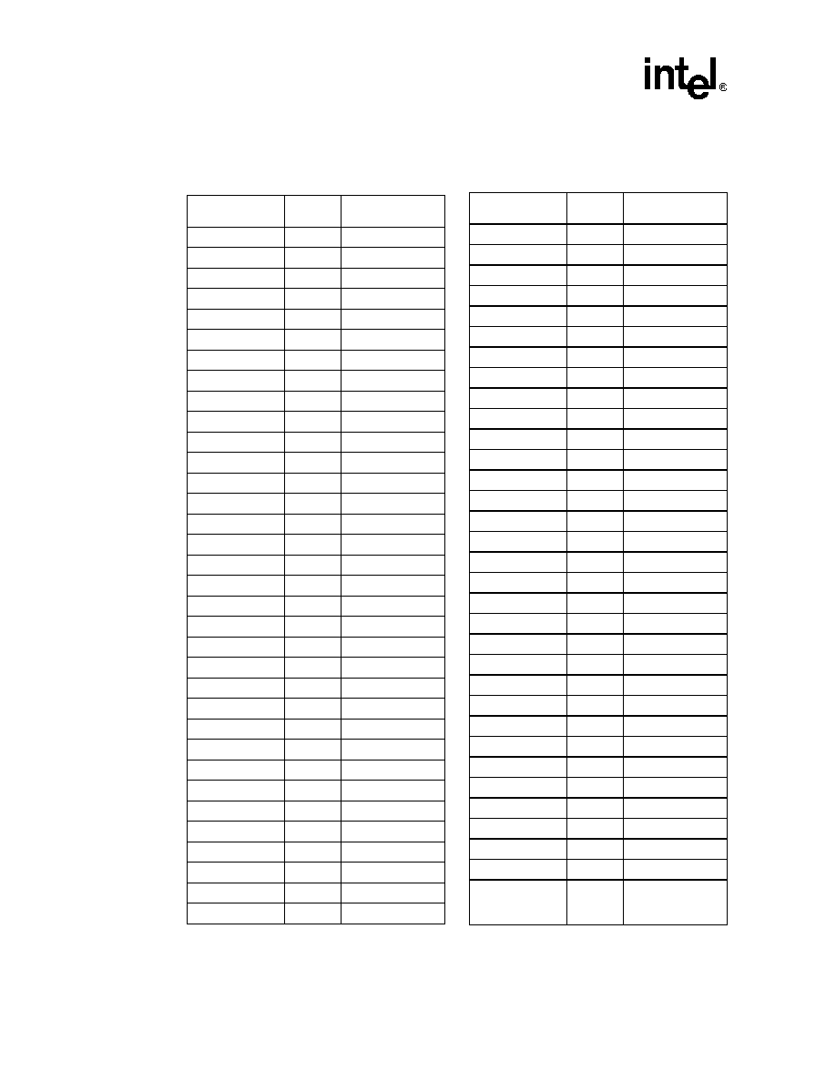
Intel
Æ
82801E C-ICH
82
Advance Information Datasheet
Table 60. XOR Chain #4; Chain 4-1 and
Chain 4-2
(RTCRST# Asserted for Seven PCI Clocks While
PWROK Active)
Pin Name
Ball #
Notes
SDIOR#
W18
SDDREQ
AC22
SDIOW#
W19
SDD_15
Y20
SDA_1
AA21
SDDACK#
V19
IRQ15
AB22
SIORDY
V20
SDA_2
W20
SDCS3#
Y21
SDA_0
AB23
SDCS1#
U19
VRMPWRGD
W21
GPIO[18]
Y22
GPIO[19]
AA23
GPIO[20]
T19
GPIO[22]
U20
GPIO[23]
T20
A20GATE
Y23
RCIN#
W23
CPUPWRGD
V22
INIT#
U21
SMI#
T21
CPUSLP#
R19
IGNNE#
V23
NMI
U22
INTR
U23
A20M#
T23
STPCLK#
T22
HL7
P19
HL5
P20
HL6
R23
HL4
N19
H1REQM
P22
H1STOP
N21
See Section 5.3.1.1
HL_STR#
N23
HL_STR
M22
See Section 5.3.1.1
H1REQI
M19
HL3
M20
HL2
L23
HL1
L21
HL0
L19
H1PAR
K22
HLCOMP
K19
Out XOR Chain 4-1
LAN1_RXD[1]
G23
In XOR Chain 4-2
LAN1_TXD[0]
H21
LAN1_TXD[1]
G21
LAN1_TXD[2]
E23
LAN1_RXD[0]
H20
EE1_DOUT
G20
LAN1_RXD[2]
E22
LAN1_RSTSYNC
D23
EE1_SHCLK
C23
EE1_DIN
E21
EE1_CS
F20
LAN0_RXD[1]
H19
LAN0_RXD[2]
B23
LAN0_RSTSYNC
C22
EE0_DOUT
D21
EE0_SHCLK
E20
EE0_CS
F19
EE0_DIN
G19
LAN0_RXD[0]
C21
LAN0_TXD[2]
D20
LAN0_TXD[1]
A22
LAN0_TXD[0]
C20
OC0#
AA1
XOR Chain #4
Output, (Chain 4-
2)
Table 60. XOR Chain #4; Chain 4-1 and
Chain 4-2
(RTCRST# Asserted for Seven PCI Clocks While
PWROK Active)
Pin Name
Ball #
Notes

Intel
Æ
82801E C-ICH
Advance Information Datasheet
83
Table 61. Signals Not in XOR Chain
Pin Name
Ball #
Notes
APICCLK
AC9
CLK14
W11
CLK48
AB8
CLK66(HCLK)
J23
PCICLK
M5
SIU_LCLK
E13
UART_CLK
A19
LAN1_CLK
B21
LAN0_CLK
F22
INTRUDER#
AB5
PWROK
W9
RSMRST#
Y8
RTCX1
Y7
RTCX2
AA7
RTCRST#
AA6
TP[2]
AC2
RSM_PWROK
T3
TP[1]
AA5
OC0#
AA1
RI#
R5
Table 61. Signals Not in XOR Chain
Pin Name
Ball #
Notes
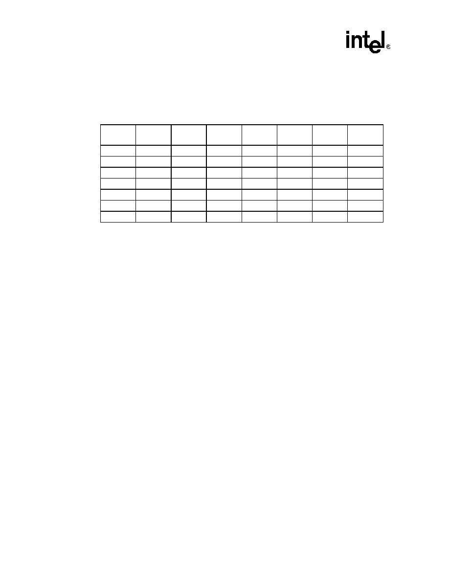
Intel
Æ
82801E C-ICH
84
Advance Information Datasheet
5.3.1
XOR Chain Testability Algorithm Example
XOR chain testing allows motherboard manufacturers to check component connectivity (e.g.,
opens and shorts to VCC or GND). An example algorithm to do this is shown in Table 62.
In this example, Vector 1 applies all "0s" to the chain inputs. The outputs being non-inverting, will
consistently produce a "1" at the XOR output on a good board. One short to Vcc (or open floating
to Vcc) will result in a "0" at the chain output, signaling a defect.
Likewise, applying Vector 7 (all "1s") to the chain inputs (given that there are an even number of
input signals in the chain), will consistently produce a "1" at the XOR chain output on a good
board. One short to Vss (or open floating to Vss) will result in a "0" at the chain output, signaling a
defect. It is important to note that the number of inputs pulled to "1" will affect the expected chain
output value. If the number of chain inputs pulled to "1" is even, then expect "1" at the output. If
the number of chain inputs pulled to "1" is odd, expect "0" at the output.
Continuing with the example in Table 62, as the input pins are driven to "1" across the chain in
sequence, the XOR Output will toggle between "0" and "1." Any break in the toggling sequence
(e.g., "1011") will identify the location of the short or open.
5.3.1.1
Test Pattern Consideration for XOR Chain 4
When the 82801E C-ICH is operated with the Hub Interface in "Normal" mode (See "Functional
Straps" on page 49), the HL_STB and HL_STB# signals must always be driven to complementary
logic levels. For example, if a "1" is driven on HL_STB, then a "0" must be driven on HL_STB#
and vice versa. This will need to be considered in applying test patterns to this chain.
When the 82801E C-ICH is operated with the Hub Interface in "Enhanced" mode there are no
restrictions on the values that may be driven onto the HL_STB and HL_STB# signals.
Table 62. XOR Test Pattern Example
Vector
Input
Pin 1
Input
Pin 2
Input
Pin 3
Input
Pin 4
Input
Pin 5
Input
Pin 6
XOR
Output
1
0
0
0
0
0
0
1
2
1
0
0
0
0
0
0
3
1
1
0
0
0
0
1
4
1
1
1
0
0
0
0
5
1
1
1
1
0
0
1
6
1
1
1
1
1
0
0
7
1
1
1
1
1
1
1