
Intel
815 Chipset Family:
82815EP and 82815P
Memory Controller Hub (MCH)
Datasheet
March 2001
Document Reference Number: 290693-002
R

82815EP and 82815P MCH
R
2
Datasheet
Information in this document is provided in connection with Intel products. No license, express or implied, by estoppel or otherwise, to any intellectual
property rights is granted by this document. Except as provided in Intel's Terms and Conditions of Sale for such products, Intel assumes no liability
whatsoever, and Intel disclaims any express or implied warranty, relating to sale and/or use of Intel products including liability or warranties relating to fitness
for a particular purpose, merchantability, or infringement of any patent, copyright or other intellectual property right. Intel products are not intended for use in
medical, life saving, or life sustaining applications.
Intel may make changes to specifications and product descriptions at any time, without notice.
Designers must not rely on the absence or characteristics of any features or instructions marked "reserved" or "undefined." Intel reserves these for future
definition and shall have no responsibility whatsoever for conflicts or incompatibilities arising from future changes to them.
The
Intel
82815EP and 82815P chipset MCH
may contain design defects or errors known as errata which may cause the product to deviate from
published specifications. Current characterized errata are available on request.
Contact your local Intel sales office or your distributor to obtain the latest specifications and before placing your product order.
I
2
C is a 2-wire communications bus/protocol developed by Philips. SMBus is a subset of the I
2
C bus/protocol and was developed by Intel. Implementations
of the I
2
C bus/protocol may require licenses from various entities, including Philips Electronics N.V. and North American Philips Corporation.
Alert on LAN is a result of the Intel-IBM Advanced Manageability Alliance and a trademark of IBM
Copies of documents which have an ordering number and are referenced in this document, or other Intel literature, may be obtained from:
Intel Corporation
www.intel.com
or call 1-800-548-4725
*Third-party brands and names are the property of their respective owners.
Copyright © 2000,2001 Intel Corporation

82815EP and 82815P MCH
R
Datasheet
3
Contents
1.
Overview .................................................................................................................................... 11
1.1.
Related Documents....................................................................................................... 11
1.2.
The Intel
815EP Chipset Family .................................................................................. 12
1.3.
82815EP MCH Overview............................................................................................... 14
1.4.
Host Interface ................................................................................................................ 15
1.5.
System Memory Interface ............................................................................................. 15
1.6.
AGP Interface................................................................................................................ 16
1.7.
Hub Interface................................................................................................................. 16
1.8
System Clocking............................................................................................................ 17
1.9
MCH Power Delivery ..................................................................................................... 17
2.
Signal Description ...................................................................................................................... 19
2.1.
Host Interface Signals ................................................................................................... 20
2.2.
System Memory Interface Signals................................................................................. 21
2.3.
AGP Interface Signals ................................................................................................... 22
2.3.1.
AGP Addressing Signals ............................................................................. 22
2.3.2.
AGP Flow Control Signals........................................................................... 23
2.3.3.
AGP Status Signals..................................................................................... 23
2.3.4.
AGP Clocking Signals (Strobes) ................................................................. 24
2.3.5.
AGP FRAME# Signals ................................................................................ 25
2.4.
Hub Interface Signals .................................................................................................... 27
2.5
Power Signals................................................................................................................ 28
2.5
Power Signals................................................................................................................ 28
2.5.
Clock Signals................................................................................................................. 28
2.6.
MCH Power-Up/Reset Strap Options............................................................................ 28
3.
Configuration Registers.............................................................................................................. 31
3.1.
Register Nomenclature and Access Attributes.............................................................. 31
3.2.
PCI Configuration Space Access .................................................................................. 31
3.2.1.
PCI Bus Configuration Mechanism ............................................................. 32
3.2.2.
Logical PCI Bus #0 Configuration Mechanism ............................................ 32
3.2.3.
Primary PCI (PCI0) and Downstream Configuration Mechanism ............... 33
3.2.4.
MCH Register Introduction .......................................................................... 33
3.3.
I/O Mapped Registers ................................................................................................... 33
3.3.1.
CONF_ADDR
Configuration Address Register ........................................ 33
3.3.2.
CONF_DATA
Configuration Data Register .............................................. 35
3.4.
Host-Hub Interface Bridge/DRAM Controller Device Registers (Device 0) ................... 36
3.4.1.
VID--Vendor Identification Register (Device 0) .......................................... 38
3.4.2.
DID--Device Identification Register (Device 0)........................................... 38
3.4.3.
PCICMD--PCI Command Register (Device 0) ........................................... 39
3.4.4.
PCISTS--PCI Status Register (Device 0)................................................... 40
3.4.5.
RID--Revision Identification Register (Device 0)........................................ 41
3.4.6.
SUBC--Sub-Class Code Register (Device 0)............................................. 41
3.4.7.
BCC--Base Class Code Register (Device 0) ............................................. 41
3.4.8.
MLT--Master Latency Timer Register (Device 0)....................................... 42
3.4.9.
HDR--Header Type Register (Device 0) .................................................... 42
3.4.10.
APBASE--Aperture Base Configuration Register (Device 0: AGP Mode
Only) ........................................................................................................ 42

82815EP and 82815P MCH
R
4
Datasheet
3.4.11.
SVID--Subsystem Vendor Identification Register (Device 0) .....................44
3.4.12.
SID--Subsystem Identification Register (Device 0) ....................................44
3.4.13.
CAPPTR--Capabilities Pointer (Device 0) ..................................................44
3.4.14.
MCHCFG--MCH Configuration Register (Device 0) ...................................45
3.4.15.
APCONT--Aperture Control (Device 0) ......................................................47
3.4.16.
DRP--DRAM Row Population Register (Device 0) .....................................48
3.4.17.
DRAMT--DRAM Timing Register (Device 0) ..............................................49
3.4.18.
DRP2--DRAM Row Population Register 2 (Device 0) ................................50
3.4.19.
FDHC--Fixed DRAM Hole Control Register (Device 0) ..............................51
3.4.20.
PAM--Programmable Attributes Map Registers (Device 0)........................51
3.4.21.
SMRAM--System Management RAM Control Register (Device 0) ...........56
3.4.22.
MISCC--Miscellaneous Control Register (Device 0) ..................................58
3.4.23.
CAPID--Capability Identification (Device 0: AGP Mode Only) ....................60
3.4.24.
BUFF_SC--System Memory Buffer Strength Control Register (Device 0) .61
3.4.25.
BUFF_SC2--System Memory Buffer Strength Control Register 2 (Device 0)64
3.4.26.
SM_RCOMP--System Memory R Compensation Control Register (Device
0) ........................................................................................................65
3.4.27.
SM--System Memory Control Register .......................................................66
3.4.28.
ACAPID--AGP Capability Identifier Register (Device 0: AGP Mode Only) 67
3.4.29.
AGPSTAT--AGP Status Register (Device 0: AGP Mode Only)..................68
3.4.30.
AGPCMD--AGP Command Register (Device 0: AGP Mode Only) ............69
3.4.31.
AGPCTRL--AGP Control Register (Device 0: AGP Mode Only) ................70
3.4.32.
APSIZE--Aperture Size (Device 0: AGP Mode Only) .................................71
3.4.33.
ATTBASE--Aperture Translation Table Base Register (Device 0: AGP
Mode Only)
........................................................................................................72
3.4.34.
AMTT--AGP Multi-Transaction Timer (Device 0: AGP Mode Only) ..........73
3.4.35.
LPTT--AGP Low Priority Transaction Timer Register (Device 0: AGP Mode
Only) ........................................................................................................74
3.4.36.
MCHCFG--MCH Configuration Register (Device 0: AGP Mode Only) ......75
3.4.37.
ERRCMD--Error Command Register (Device 0: AGP Mode Only) ...........76
3.5.
AGP/PCI Bridge Registers (Device 1: Visible in AGP Mode Only) ...............................78
3.5.1.
VID1--Vendor Identification Register (Device 1).........................................79
3.5.2.
DID1--Device Identification Register (Device 1) .........................................79
3.5.3.
PCICMD1--PCI-PCI Command Register (Device 1) ..................................79
3.5.4.
PCISTS1--PCI-PCI Status Register (Device 1) ..........................................81
3.5.5.
RID1--Revision Identification Register (Device 1) ......................................82
3.5.6.
SUBC1--Sub-Class Code Register (Device 1) ...........................................82
3.5.7.
BCC1--Base Class Code Register (Device 1) ............................................82
3.5.8.
MLT1--Master Latency Timer Register (Device 1) .....................................83
3.5.9.
HDR1--Header Type Register (Device 1)...................................................83
3.5.10.
PBUSN--Primary Bus Number Register (Device 1)....................................83
3.5.11.
SBUSN--Secondary Bus Number Register (Device 1)...............................84
3.5.12.
SUBUSN--Subordinate Bus Number Register (Device 1) ..........................84
3.5.13.
SMLT--Secondary Master Latency Timer Register (Device 1)...................85
3.5.14.
IOBASE--I/O Base Address Register (Device 1)........................................86
3.5.15.
IOLIMIT--I/O Limit Address Register (Device 1).........................................87
3.5.16.
SSTS--Secondary PCI-PCI Status Register (Device 1) .............................88
3.5.17.
MBASE--Memory Base Address Register (Device 1) ................................89
3.5.18.
MLIMIT--Memory Limit Address Register (Device 1) .................................90
3.5.19.
PMBASE--Prefetchable Memory Base Address Register (Device 1).........91
3.5.20.
PMLIMIT--Prefetchable Memory Limit Address Register (Device 1)..........92
3.5.21.
BCTRL--PCI-PCI Bridge Control Register (Device 1) ................................93
3.5.22.
ERRCMD1--Error Command Register (Device 1)......................................95
4.
Functional Description ................................................................................................................97

82815EP and 82815P MCH
R
Datasheet
5
4.1.
System Address Map .................................................................................................... 97
4.1.1.
Memory Address Ranges............................................................................ 98
4.1.2.
Compatibility Area ....................................................................................... 99
4.1.3.
Extended Memory Area............................................................................. 102
4.1.3.1.
System Management Mode (SMM) Memory Range .................... 105
4.2.
Memory Shadowing..................................................................................................... 106
4.3.
I/O Address Space ...................................................................................................... 106
4.3.1.
MCH Decode Rules and Cross-Bridge Address Mapping ........................ 106
4.3.2.
Address Decode Rules.............................................................................. 107
4.3.2.1.
AGP Interface Decode Rules ....................................................... 108
4.3.2.2.
Legacy VGA Ranges .................................................................... 109
4.4.
Host Interface .............................................................................................................. 110
4.4.1.
Host Bus Device Support .......................................................................... 110
4.4.2.
Special Cycles ........................................................................................... 112
4.5.
System Memory DRAM Interface................................................................................ 113
4.5.1.
DRAM Organization and Configuration ..................................................... 113
4.5.1.1.
Configuration Mechanism For DIMMs .......................................... 114
4.5.1.2.
DRAM Register Programming...................................................... 115
4.5.2.
DRAM Address Translation and Decoding ............................................... 115
4.5.3.
DRAM Array Connectivity.......................................................................... 116
4.5.4.
SDRAMT Register Programming .............................................................. 117
4.5.5.
SDRAM Paging Policy............................................................................... 117
4.6.
System Reset for the MCH.......................................................................................... 117
4.7.
System Clock Description ........................................................................................... 117
4.8.
Power Management .................................................................................................... 118
4.8.1.
Specifications Supported........................................................................... 118
5.
Pinout and Package Information.............................................................................................. 119
5.1.
82815EP MCH Pinout ................................................................................................. 119
5.2.
Package Information ................................................................................................... 126
6.
Testability ................................................................................................................................. 129
6.1.
XOR Tree Testability Algorithm Example.................................................................... 130
6.1.1.
Test Pattern Consideration for XOR Chains 3 and 4, and 7 and 8 ........... 130
6.2.
XOR Tree Initialization................................................................................................. 131
6.2.1.
Chain [1:6] Initialization ............................................................................. 131
6.2.2.
Chain [7:8] Initialization ............................................................................. 131
6.3.
XOR Chain .................................................................................................................. 132
6.4.
All Z ............................................................................................................................. 137

82815EP and 82815P MCH
R
6
Datasheet
Figures
Figure 1. Intel
815EP Chipset Family System Block Diagram................................................13
Figure 2. 82815EP MCH Block Diagram ..................................................................................14
Figure 3. PAM Registers ..........................................................................................................53
Figure 4. System Memory Address Map ..................................................................................98
Figure 5. Detailed Memory System Address Map ....................................................................98
Figure 6. DRAM Array Sockets ..............................................................................................116
Figure 7. MCH Pinout (Top View-Left Side) ...........................................................................120
Figure 8. MCH Pinout (Top View-Right Side) .........................................................................121
Figure 9. MCH BGA Package Dimensions (Top and Side Views) .........................................126
Figure 10. MCH BGA Package Dimensions (Bottom View) ...................................................127
Figure 11. XOR Tree Implementation ....................................................................................129
Tables
Table 1. Supported System Bus and System Memory Bus Frequencies.................................17
Table 2. MCH PCI Configuration Space (Device 0) .................................................................36
Table 3. Supported System Memory DIMM Configurations .....................................................48
Table 4. Attribute Bit Assignments ...........................................................................................52
Table 5. PAM Registers and Associated Memory Segments...................................................53
Table 6. Summary of MCH Error Sources, Enables and Status Flags.....................................77
Table 7. MCH Configuration Space (Device 1) ........................................................................78
Table 8. Memory Segments and Their Attributes .....................................................................99
Table 9. Summay of Transactions Supported By MCH..........................................................110
Table 10. Host Responses Supported by the MCH................................................................111
Table 11. Special Cycles ........................................................................................................112
Table 12. Sample Of Possible Mix And Match Options For 4 Row/2 DIMM Configurations ..114
Table 13. Data Bytes on DIMM Used for Programming DRAM Registers .............................115
Table 14. MCH DRAM Address Mux Function .......................................................................116
Table 15. Programmable SDRAM Timing Parameters ..........................................................117
Table 16. Alphabetical Pin Assignment ..................................................................................122
Table 17. Package Dimensions..............................................................................................127
Table 18. XOR Test Pattern Example ....................................................................................130
Table 19
XOR Chain 1 35 Inputs Output: SMAA5 (A12).......................................................132
Table 20
XOR Chain 2 33 Inputs Output: SMAA2 (F12).......................................................132
Table 21
XOR Chain 3 38 Inputs Output: SMAA0 (D13) ......................................................133
Table 22
XOR Chain 4 36 Inputs Output: SMAA9 (D13) ......................................................133
Table 23
XOR Chain 5 56 Inputs Output: SMD31 (K5).........................................................134
Table 24
XOR Chain 6 60 Inputs Output: SMAA11 (A13).....................................................135
Table 25
XOR Chain 7 33 Inputs Output: SMAA8 (D12) ......................................................136
Table 26
XOR Chain 8 31 Inputs Output: SMAA4 (B12).......................................................136
82815EP and 82815P MCH
R
Datasheet
7
Revision History
Rev. Description
Date
-001 Initial
Release
November 2000
-002
Added 82815P MCH references; added IntelÆ 815 Chipset Family information to
the Overview section
March 2001

82815EP and 82815P MCH
R
8
Datasheet
This page is intentionally left blank.

82815EP and 82815P MCH
R
Datasheet
9
82815EP MCH Features
!
Processor/Host Bus Support
Intel
Pentium
III
processor and Intel
Æ
CeleronTM
Processor in FC-PGA package
Supports processor 370-Pin Socket
Supports 32-Bit System Bus Addressing
4 deep in-order queue; 4 or 1 deep request queue
Supports Uni-processor systems only
In-order and Dynamic Deferred Transaction Support
66/100/133MHz System Bus Frequency
GTL+ I/O Buffer
!
Integrated SDRAM Controller
32 MB to 512 MB using 16Mb/64Mb/128Mb/256Mb
technology
Supports up to 3 double sided DIMMs at 100 MHz system
memory bus
Supports up to 2 double sided or 3 single sided DIMMs at
133 MHz system memory bus.
64-bit data interface
100/133 MHz system memory bus frequency
Support for Asymmetrical SDRAM addressing only
Support for x8 and x16 SDRAM device width
Unbuffered, Non-ECC SDRAM only supported
Refresh Mechanism: CBR ONLY supported
Enhanced Open page arbitration SDRAM paging scheme
Suspend to RAM support
!
Accelerated Graphics Port (AGP) Interface
Supports a single AGP device via a connector
Supports AGP 2.0 including 4x AGP data transfers
AGP Universal Connector support via dual mode buffers
to allow AGP 2.0 3.3V or 1.5V signaling
AGP PIPE# or SBA initiated accesses to SDRAM not
snooped
AGP FRAME# initiated accesses to SDRAM are snooped
High priority access support
Hierarchical PCI configuration mechanism
Delayed transaction support for AGP-to-SDRAM reads
that can not be serviced immediately
!
Arbitration Scheme and Concurrency
Intelligent Centralized Arbitration Model for Optimum
Concurrency Support
Concurrent operations of processor and System busses
supported via dedicated arbitration and data buffering
!
Data Buffering
Distributed Data Buffering Model for optimum
concurrency
SDRAM Write Buffer with read-around-write capability
Dedicated processor ≠SDRAM, hub interface-SDRAM
and Graphics-SDRAM Read Buffers
!
Power Management Functions
SMRAM space remapping to A0000h (128 KB)
Optional Extended SMRAM space above 256 MB,
additional 512 KB / 1MB TSEG from Top of Memory,
cacheable
Stop Clock Grant and Halt special cycle translation from
the host to the hub interface
ACPI Compliant power management
APIC Buffer Management
SMI, SCI, and SERR error indication
!
Supporting I/O Bridge
82801AA I/O Controller Hub (ICH)
82801BA I/O Controller Hub (ICH2)
!
Packaging/Power
544 BGA
1.85V core with 3.3V CMOS I/O

82815EP and 82815P MCH
R
10
Datasheet
82815EP MCH Simplified Block Diagram
HA[31:3]#
HD[63:0]#
ADS#
BNR#
BPRI#
DBSY#
DEFER#
DRDY#
HIT#
HITM#
HLOCK#
HREQ[4:0]#
HTRDY#
RS[2:0]#
CPURST#
Host Bus
Interface
SMAA[12:0]
SMAB[7:4]#
SBS[1:0]
SMD[63:0]
SDQM[7:0]
SCSA[5:0]#
SRAS#
SCAS#
SWE#
SCKE[5:0]
System
Memory
Interface
Hub
Interface
HLREF
HL[10:0]
HLSTRB
HLSTRB#
HLZCOMP
Clock
And Reset
HCLK
SCLK
LTCLK[1:0]
LOCLK
LRCLK
DCLKREF
HLCLK
RESET#
AGP
Interface
SMAC[7:4]#
SCSB[5:0]#
PIPE#
SBA[7:0]
RBF#
WBF#
ST[2:0]
AD_STB[1:0]
AD_STB[1:0]#
G_FRAME#
G_IRDY#
G_TRDY#
G_STOP#
G_DEVSEL#
G_REQ#
G_GNT#
G_AD[31:0]#
G_C/BE[3:0]#
G_PAR
AGPREF
SB_STB
SB_STB#
GRCOMP
SRCOMP
GTLREF[1:0]
Signals

82815EP and 82815P MCH
R
Datasheet
11
1. Overview
The Intel
815EP chipset family is a high-flexibility chipset designed to extend from the basic
graphics/multimedia PC platform up to the mainstream performance desktop platform. The chipset
consists of a 82815EP Memory Controller Hub (MCH) and an I/O Controller Hub for the I/O subsystem.
The MCH integrates a system memory SDRAM controller that supports a 64-bit 100/133 MHz SDRAM
array.
The 82815EP MCH integrates an AGP controller interface to enable graphics configuration and upgrade
flexibility with the Intel
815EP chipset family.
There are four chipsets in the Intel
Æ
815 chipset family:
∑
Intel
Æ
82815 chipset: This chipset contains the 82815 and the 82801AA ICH.
∑
Intel
Æ
82815E chipset: This chipset contains the 82815E and the 82801BA ICH2.
∑
Intel
Æ
82815EP chipset: This chipset contains the 82815EP and the 82801BA ICH2. There is no
internal graphics capability. This MCH uses an AGP port only.
∑
Intel
Æ
82815P chipset: This chipset contains the 82815P and the 82801AA (ICH) and IntelÆ
82801AB (ICH0). There is no internal graphics capability. This MCH uses an AGP port only.
The only component difference between the Intel
Æ
82815 GMCH and the Intel
Æ
82815E GMCH is the
I/O Controller Hub.
This datasheet provides an overview of the 815EP chipset family (see Section 1.2). The remainder of the
document describes the Intel
82815EP Memory Controller Hub (MCH).
The Intel
815EP chipset family may contain design defects or errors known as errata which may cause the product to deviate
from published specifications. Current characterized errata are available on request.
1.1. Related Documents
∑
I/O Specification: Contained in the Intel
Pentium
II Processor Datasheet
∑
PCI Local bus Specification 2.2: Contact
www.pcisig.com
∑
Intel
Æ
82801AA (ICH) and Intel
Æ
82801AB (ICH0) I/O Controller Hub Datasheet
(Document Number 290655)
∑
Intel
Æ
82801BA I/O Controller Hub (ICH2) Datasheet (Document Number 290687)
∑
Intel
Æ
82802 Firmware Hub (FWH) Datasheet (Document Number 290658)
∑
Intel
Æ
815EP Chipset Design Guide (Document Number 290692)
∑
Intel
Æ
815 Chipset Family: 82815EP and 82815P Memory Controller Hub (MCH)
Specification Update (Document Number 290695)

82815EP and 82815P MCH
R
12
Datasheet
1.2. The Intel
815EP Chipset Family
Figure 1 shows a typical system block diagram based on the Intel
Æ
815EP chipset family. The chipset
uses a hub architecture with the MCH as the host bridge hub and the I/O Controller Hub as the I/O hub.
The MCH supports processor bus frequencies of 66/100/133 MHz. The I/O Controller Hub is highly
integrated providing many of the functions needed in today's PC platforms; it also provides the interface
to the PCI Bus. The MCH and I/O Controller Hub communicate over a dedicated hub interface.
82801BA ICH2 functions include:
∑
PCI Rev 2.2 compliant with support for 33 MHz PCI operations
∑
Supports up to 6 Req/Gnt pairs (PCI Slots)
∑
Power management logic support
∑
Enhanced DMA controller, interrupt controller, and timer functions
∑
Integrated IDE controller
Ultra ATA/100/66/33
∑
USB host interface
2 host controllers and supports 4 USB ports
∑
Integrated LAN controller
∑
System Management Bus (SMBus) compatible with most I
2
C devices
ICH2 has both bus master and slave capability
∑
AC'97 2.1 compliant link for audio and telephony codecs
Up to 6 channels
∑
Low Pin Count (LPC) interface
∑
Firmware Hub (FWH) interface support
Intel's FWH component is the 82802: It contains a Random Number Generator (RNG), five
General Purpose Inputs (GPIs), register-based block locking, hardware-based locking, and
Flash memory for platform code/data nonvolatile storage
FWH component is also available from other suppliers
∑
Alert on LAN*
AOL
AOL2
82815EP and 82815P MCH
R
Datasheet
13
Figure 1. Intel
815EP Chipset Family System Block Diagram
Hub
Interface
System Bus (66/100/133 MHz)
815_SysBlk
Intel
Æ
Pentium
Æ
III Processor
or
Intel
Æ
CeleronTM Processor
AGP Connector
AGP
Graphics
System
Memory
82815EP MCH
(Memory Controller
Hub)
- Memory Controller
- AGP Contoller
64 Bit /
100/133 MHz Only
Intel
Æ
815EP Chipset family
I/O Controller Hub
82801BA ICH2)
PCI Bus
4 USB Ports; 2 HC (ICH2)
UltraATA/100/66/33 (ICH2)
AC'97 Codec(s)
(optional)
AC'97 2.1
LPC I/F
Super I/O
Keyboard,
Mouse, FD, PP,
SP, IR
FWH
PCI
Slots
PCI
Agent
GPIO
LAN Connect
4 IDE Drives
AGP 2.0

82815EP and 82815P MCH
R
14
Datasheet
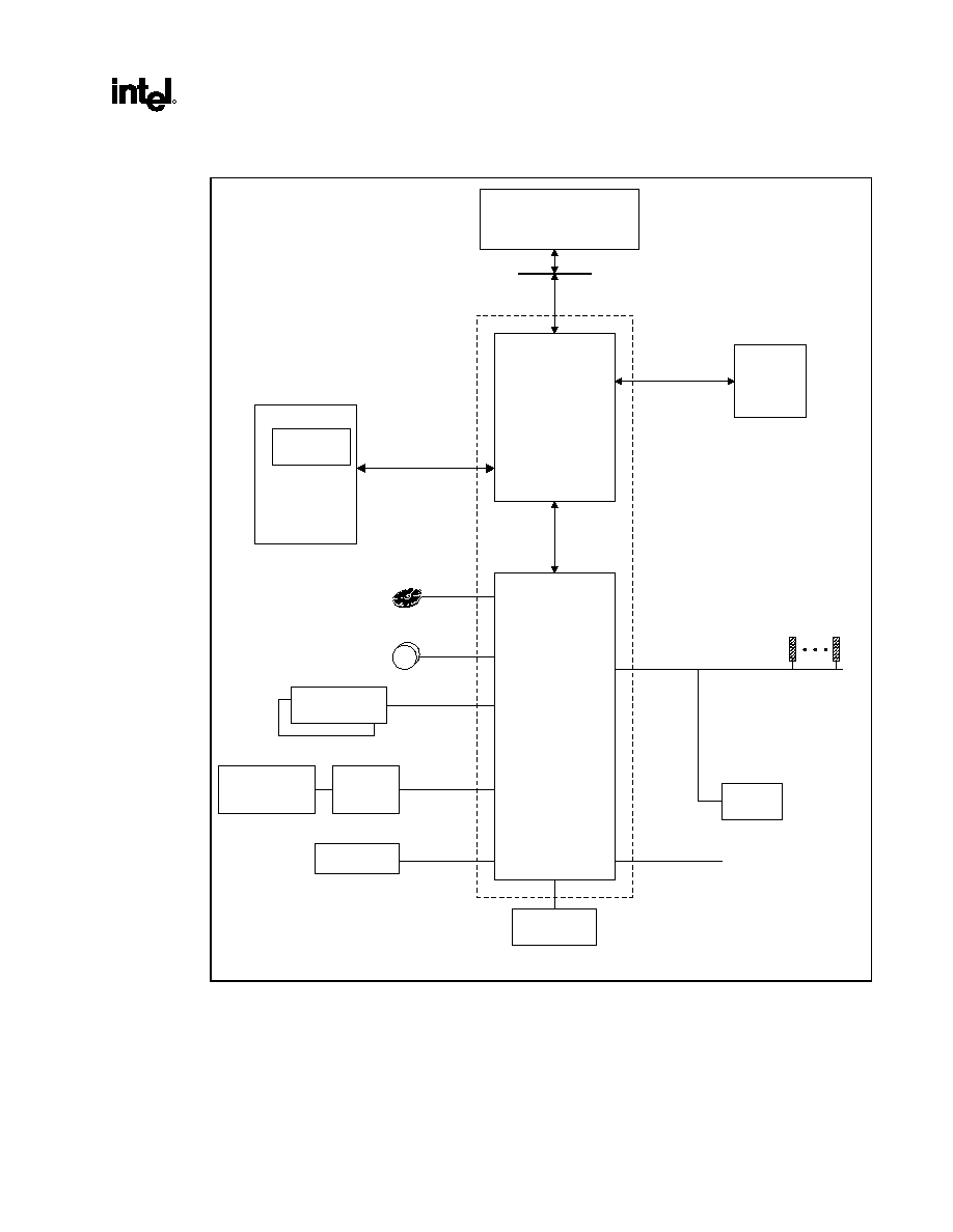
1.3. 82815EP MCH Overview
Figure 2 is a block diagram of the MCH illustrating the various interfaces and integrated functions. The
functions and capabilities include:
∑
Support for a single processor configuration
∑
64-bit AGTL+ based System Bus Interface at 66/100/133 MHz
∑
32-bit Host Address Support
∑
64-bit System Memory Interface with optimized support for SDRAM at 100/133 MHz
∑
AGP 1X/2X/4X Controller
Figure 2. 82815EP MCH Block Diagram
System Bus Interface
Buffer
Memory Interface
Buffer
Hub Interface
System
Memory
gmch_blk2.vsd
AGP Interface
Local Memory
Interface
AGP
Pins

82815EP and 82815P MCH
R
Datasheet
15
1.4. Host Interface
The host interface of the MCH is optimized to support the Intel
Pentium
Æ
III
processor and Intel
Celeron
TM
processor in the FC-PGA package. The MCH implements the host address, control, and data
bus interfaces within a single device. The MCH supports a 4-deep in-order queue (i.e., supports
pipelining of up to 4 outstanding transaction requests on the host bus) . Host bus addresses are decoded
by the MCH for accesses to system memory, PCI memory and PCI I/O (via hub interface), PCI
configuration space and Graphics memory. The MCH takes advantage of the pipelined addressing
capability of the processor to improve the overall system performance.
The 82815EP MCH supports the 370-pin socket processor.
∑
370-pin socket (PGA370). The PGA370 is a zero insertion force (ZIF) socket that a processor in
the FC-PGA package will use to interface with a system board.
1.5. System Memory Interface
The MCH integrates a system memory controller that supports a 64-bit 100/133 MHz SDRAM array.
The only DRAM type supported is industry standard Synchronous DRAM (SDRAM). The SDRAM
controller interface is fully configurable through a set of control registers.
The MCH supports industry standard 64-bit wide DIMMs with SDRAM devices. The thirteen
multiplexed address lines (SMAA[12:0]) along with the two bank select lines (SBS[1:0]) allow the MCH
to support 2M, 4M, 8M, 16M, and 32M x64 DIMMs. Only asymmetric addressing is supported. The
MCH has 6 SCS# lines (2 copies of each for electrical loading), enabling the support of up to six 64-bit
rows of SDRAM. The MCH targets SDRAM with CL2 and CL3, and supports both single and double-
sided DIMMs. Additionally, the MCH also provides a 1024 deep refresh queue. The MCH can be
configured to keep up to 4 pages open within the memory array. Pages can be kept open in any one bank
of memory.
The Intel
815EP chipset family supports up to 3 DIMM connectors in a system. A maximum of 2
double-sided or 3 single-sided DIMMs may be populated when the SDRAM interface is operating at
133 MHz. Upon detection that additional rows are populated beyond these configurations, the BIOS
must down-shift the SDRAM clocks to 100 MHz through a two-wire interface of the system clock
generator.
SCKE[5:0] is used in configurations requiring powerdown mode for the SDRAM.

82815EP and 82815P MCH
R
16
Datasheet
1.6. AGP Interface
A single AGP connector is supported by the MCH AGP interface. The AGP buffers operate in one of
two selectable modes in order to support the AGP Universal Connector:
∑
3.3V drive, not 5 volt safe: This mode is compliant to the AGP 1.0 and 2.0 specifications.
∑
1.5V drive, not 3.3 volt safe: This mode is compliant with the AGP 2.0 specification.
The following table shows the AGP Data Rate and the Signaling Levels supported by the MCH.
Signaling Level
Data Rate
1.5V 3.3V
1x AGP
Yes
Yes
2x AGP
Yes
Yes
4x AGP
Yes
No
The AGP interface supports 4x AGP signaling. The Intel 82815EP only supports AGP4X cards that use
differential clocking mode.
AGP semantic (PIPE# or SBA[7:0]) cycles to SDRAM are not snooped on the host bus. AGP FRAME#
cycles to SDRAM are snooped on the host bus. The MCH supports PIPE# or SBA[7:0] AGP address
mechanisms, but not both simultaneously. Either the PIPE# or the SBA[7:0] mechanism must be selected
during system initialization. High priority accesses are supported. Only memory writes from the hub
interface to AGP are allowed. No transactions from AGP to the hub interface are allowed.
1.7. Hub Interface
The hub interface is a private interconnect between the MCH and the I/O Controller Hub.

82815EP and 82815P MCH
R
Datasheet
17
1.8 System
Clocking
The 82815EP MCH has a new type of clocking architecture. It has integrated SDRAM buffers that run at
either 100 or 133 MHz, independent of the system bus frequency. See table below for supported system
bus and system memory bus frequencies. The system bus frequency is selectable between 66 MHz,
100 MHz, or 133 MHz. The MCH uses a copy of the USB clock as the DOT Clock input for the graphics
pixel clock PLL.
Table 1. Supported System Bus and System Memory Bus Frequencies
Front Side Bus
Frequency
System Memory
Bus Frequency
Display Cache Interface
Frequency
66 MHz
100 MHz
133 MHz or DVMT
100 MHz
100 MHz
133 MHz or DVMT
133 MHz
100 MHz
133 MHz or DVMT
133 MHz
133 MHz
3 MHz or DVMT
1.9
MCH Power Delivery
The 82815EP MCH core voltage is 1.85V. System memory operates from a 3.3V supply. AGP 1X/2X
I/O can operate from either a 3.3V or a 1.5V supply. AGP 4X I/O requires a 1.5V supply. The AGP
interface voltage is determined by the VDDQ generation on the motherboard.

82815EP and 82815P MCH
R
18
Datasheet
This page intentionally left blank

82815EP and 82815P MCH
R
Datasheet
19
2. Signal
Description
This section provides a detailed description of the MCH signals. The signals are arranged in functional
groups according to their associated interface. The states of all of the signals during reset are provided in
the System Reset section.
The "#" symbol at the end of a signal name indicates that the active, or asserted state occurs when the
signal is at a low voltage level. When "#" is not present after the signal name the signal is asserted when
at the high voltage level.
The following notations are used to describe the signal type:
I Input
pin
O Output
pin
I/OD
Input / Open Drain Output pin. This pin requires a pullup
I/O
Bi-directional Input/Output pin
s/t/s
Sustained Tristate. This pin is driven to its inactive state prior to tri-stating.
As/t/s
Active Sustained Tristate. This applies to some of the hub interface signals. This pin
is weakly driven to its last driven value.
The signal description also includes the type of buffer used for the particular signal:
AGTL+
Open Drain AGTL+ interface signal. Refer to the AGTL+ I/O Specification for
complete details
AGP
AGP interface signals. These signals can be programmed to be compatible with AGP
2.0 3.3V or 1.5V Signaling Environment DC and AC Specifications. In 3.3V mode
the buffers are not 5V tolerant. In 1.5V mode the buffers are not 3.3V tolerant.
CMOS
The CMOS buffers are low voltage TTL compatible signals. These are 3.3V only.
LVTTL
Low Voltage TTL compatible signals. There are 3.3V only.
1.8V
1.8V signals for the digital video interface
Analog
Analog CRT Signals
Note that the processor address and data bus signals (Host Interface) are logically inverted signals
(i.e., the actual values are inverted of what appears on the processor bus). This must be taken into
account and the addresses and data bus signals must be inverted inside the MCH. All processor control
signals follow normal convention. A 0 indicates an active level (low voltage) if the signal is followed by
a # symbol and a 1 indicates an active level (high voltage) if the signal has no # suffix.

82815EP and 82815P MCH
R
20
Datasheet
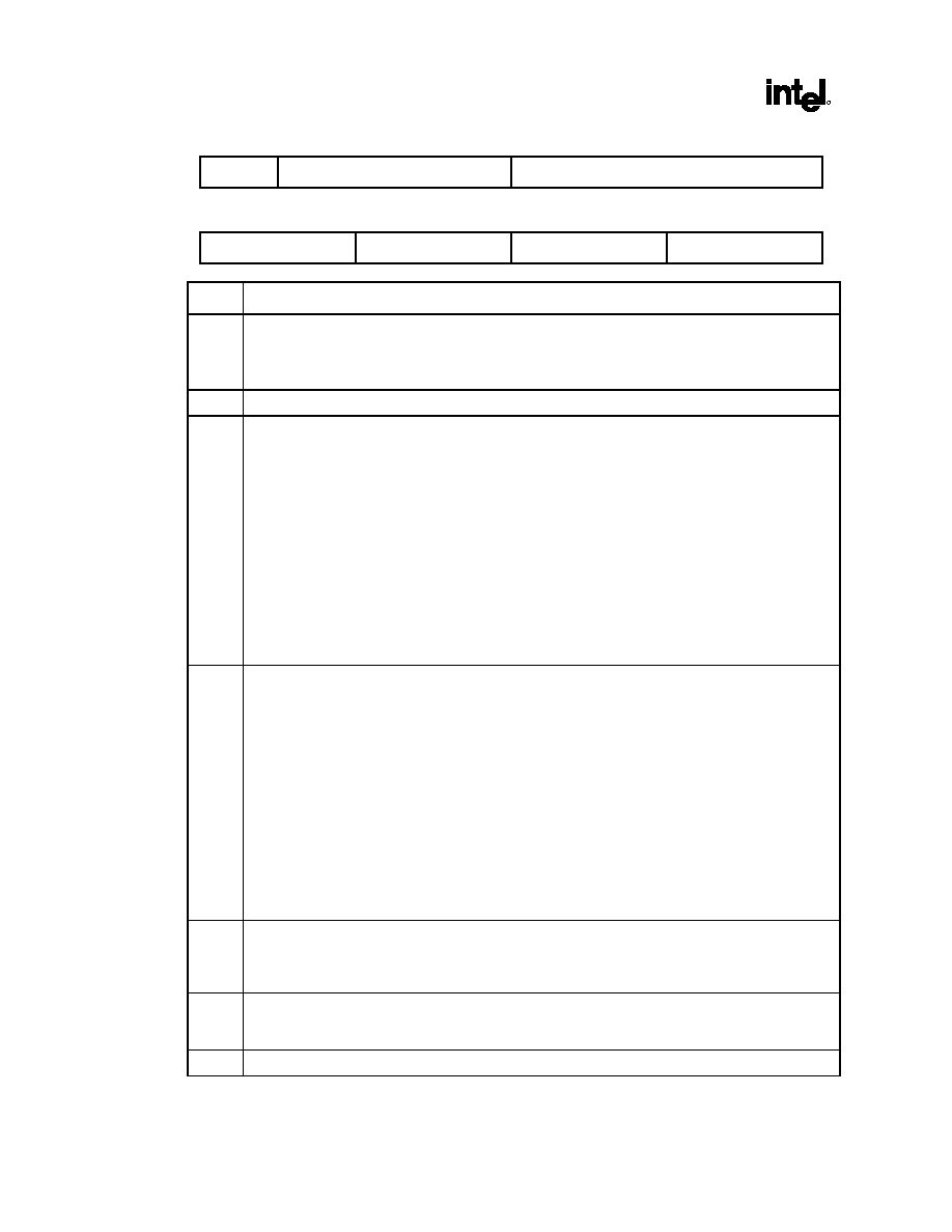
2.1. Host Interface Signals
Signal Name
Type
Description
CPURST# O
AGTL+
CPU Reset. The MCH asserts CPURST# while RESET# (PCIRST# from the I/O
Controller Hub) is asserted and for approximately 1 ms after RESET# is deasserted.
The MCH also pulses CPURST# for approximately 1 ms when requested via a hub
interface special cycle. The CPURST# allows the processor to begin execution in a
known state.
HA[31:3]# I/O
AGTL+
Host Address Bus. HA[31:3]# connect to the processor address bus. During
processor cycles, HA[31:3]# are inputs. The MCH drives HA[31:3]# during snoop
cycles on behalf of Primary PCI. Note that the address bus is inverted on the
processor bus.
HD[63:0]# I/O
AGTL+
Host Data. These signals are connected to the processor data bus. Note that the
data signals are inverted on the processor bus.
ADS# I/O
AGTL+
Address Strobe. The processor bus owner asserts ADS# to indicate the first of two
cycles of a request phase.
BNR# I/O
AGTL+
Block Next Request. Used to block the current request bus owner from issuing a
new request. This signal is used to dynamically control the processor bus pipeline
depth.
BPRI# O
AGTL+
Priority Agent Bus Request. The MCH is the only priority agent on the processor
bus. It asserts this signal to obtain the ownership of the address bus. This signal
has priority over symmetric bus requests and will cause the current symmetric
owner to stop issuing new transactions unless the HLOCK# signal was asserted.
DBSY# I/O
AGTL+
Data Bus Busy. Used by the data bus owner to hold the data bus for transfers
requiring more than one cycle.
DEFER# O
AGTL+
Defer. The MCH will generate a deferred response as defined by the rules of the
MCH dynamic defer policy. The MCH will also use the DEFER# signal to indicate a
processor retry response.
DRDY# I/O
AGTL+
Data Ready. Asserted for each cycle that data is transferred.
HIT# I/O
AGTL+
Hit. Indicates that a caching agent holds an unmodified version of the requested
line. Also driven in conjunction with HITM# by the target to extend the snoop
window.
HITM# I/O
AGTL+
Hit Modified. Indicates that a caching agent holds a modified version of the
requested line and that this agent assumes responsibility for providing the line.
HITM# is also driven in conjunction with HIT# to extend the snoop window.
HLOCK# I
AGTL+
Host Lock. All processor bus cycles sampled with the assertion of HLOCK# and
ADS#, until the negation of HLOCK# must be atomic (i.e., no hub interface or MCH
graphics snoopable access to SDRAM is allowed when HLOCK# is asserted by the
processor).
HREQ[4:0]# I/O
AGTL+
Host Request Command. Asserted during both clocks of request phase. In the first
clock, the signals define the transaction type to a level of detail that is sufficient to
begin a snoop request. In the second clock, the signals carry additional information
to define the complete transaction type.
The transactions supported by the MCH are defined in the Host Interface section of
this document.
HTRDY# I/O
AGTL+
Host Target Ready. Indicates that the target of the processor transaction is able to
enter the data transfer phase.

82815EP and 82815P MCH
R
Datasheet
21
Signal Name
Type
Description
RS[2:0]# I/O
AGTL+
Response Signals. Indicates type of response as shown below:
000 = Idle state
001 = Retry response
010 = Deferred response
011 = Reserved (not driven by the MCH)
100 = Hard Failure (not driven by the MCH)
101 = No data response
110 = Implicit Writeback
111 = Normal data response
GTLREF[1:0] I GTL Reference. Reference voltage input for the Host GTL interface. GTLREF is
2/3 * VTT. VTT is nominally 1.5V.
2.2. System Memory Interface Signals
Signal Name
Type
Description
SMAA[12:0]
SMAB[7:4]#
SMAC[7:4]#
SBS[1:0]
O
CMOS
Memory Address. SMAA[12:0], SMAB[7:4]#, and SMAC[7:4]# are used to provide
the multiplexed row and column address to SDRAM. SBS[1:0] provide the Bank
Select.
SBS[1:0] O
CMOS
Memory Bank Select. These signals define the banks that are selected within
each DRAM row. The SMAx and SBS signals combine to address every possible
location within a DRAM device.
SBS[1:0] may be heavily loaded and require 2 SDRAM clock cycles for setup time
to the SDRAMs. For this reason, all chip select signals (SCSA[5:0]# and
SCSB[5:0]#) must be deasserted on any SDRAM clock cycle that one of these
signals change.
SMD[63:0] I/O
CMOS
Memory Data. These signals are used to interface to the SDRAM data bus.
SDQM[7:0] O
CMOS
Input/Output Data Mask. These pins act as synchronized output enables during
read cycles and as a byte enables during write cycles.
SCSA[5:0]#
SCSB[5:0]#
O
CMOS
Chip Select. For the memory row configured with SDRAM, these pins perform the
function of selecting the particular SDRAM components during the active state.
SRAS# O
CMOS
SDRAM Row Address Strobe. These signals drive the SDRAM array directly
without any external buffers.
SCAS# O
CMOS
SDRAM Column Address Strobe. These signals drive the SDRAM array directly
without any external buffers.
SWE# O
CMOS
Write Enable Signal. SWE# is asserted during writes to SDRAM.
SCKE[5:0] O
CMOS
System Memory Clock Enable. SCKE SDRAM Clock Enable is used to signal a
self-refresh or power-down command to an SDRAM array when entering system
suspend.
SRCOMP O
System Memory RCOMP. Used to calibrate the System memory I/O buffers. This
pin should be connected to a 40 ohm resistor tied to 3.3V VCC (VSUS3.3).

82815EP and 82815P MCH
R
22
Datasheet
2.3. AGP Interface Signals
For more details on the operation of these signals, refer to the AGP Interface Specification Revision 2.0.
82815EP AGP inteface signals function as documented in this section.
2.3.1.
AGP Addressing Signals
There are two mechanisms that the AGP master can enqueue AGP requests: PIPE# and SBA (side-band
addressing). Upon initialization, one of the methods is chosen. The master may not switch methods
without a full reset of the system. When
PIPE#
is used to enqueue addresses, the master is not allowed to
queue addresses using the SBA bus. For example, during configuration time, if the master indicates that
it can use either mechanism, the configuration software will indicate which mechanism the master will
use. Once this choice has been made, the master will continue to use the mechanism selected until the
system is reset (and reprogrammed) to use the other mode. This change of modes is not a dynamic
mechanism but rather a static decision when the device is first being configured after reset.
Signal Name
Type
Description
PIPE# I
AGP
Pipeline.
During PIPE# Operation. This signal is asserted by the AGP master to indicate a
full-width address is to be enqueued on by the target using the AD bus. One
address is placed in the AGP request queue on each rising clock edge while PIPE#
is asserted.
During SBA Operation. This signal is not used if SBA (Side Band Addressing) is
selected.
During FRAME# Operation. This signal is not used during AGP FRAME#
operation.
SBA[7:0] I
AGP
Side-band Addressing.
During PIPE# Operation. These signals are not used during PIPE# operation.
During SBA Operation. These signals (the SBA, or side-band addressing, bus) are
used by the AGP master (graphics component) to place addresses into the AGP
request queue. The SBA bus and AD bus operate independently. That is,
transactions can proceed on the SBA bus and the AD bus simultaneously.
During FRAME# Operation. These signals are not used during AGP FRAME#
operation.

82815EP and 82815P MCH
R
Datasheet
23
2.3.2.
AGP Flow Control Signals
Signal Name
Type
Description
RBF# I
AGP
Read Buffer Full.
During PIPE# and SBA Operation. Read buffer full indicates if the master is ready
to accept previously requested low priority read data. When RBF# is asserted the
MCH is not allowed to initiate the return low priority read data. That is, the MCH can
finish returning the data for the request currently being serviced, however it can not
begin returning data for the next request. RBF# is only sampled at the beginning of
a cycle.
If the AGP master is always ready to accept return read data, then it is not required
to implement this signal.
During FRAME# Operation. This signal is not used during AGP FRAME#
operation.
WBF# I
AGP
Write-Buffer Full.
During PIPE# and SBA Operation. Write bufffer full indicates if the master is ready
to accept Fast Write data from the MCH. When WBF# is asserted the MCH is not
allowed to drive Fast Write data to the AGP master. WBF# is only sampled at the
beginning of a cycle.
If the AGP master is always ready to accept fast write data, then it is not required to
implement this signal.
During FRAME# Operation: This signal is not used during AGP FRAME#
operation.
2.3.3.
AGP Status Signals
Signal Name
Type
Description
ST[2:0] O
AGP
Status Bus.
During PIPE# and SBA Operation. Provides information from the arbiter to a AGP
Master on what it may do. ST[2:0] only have meaning to the master when its GNT#
is asserted. When GNT# is deasserted, these signals have no meaning and must
be ignored. Refer to the AGP Interface Specificaiton revision 2.0 for further
explanation of the ST[2:0] values and their meanings.
During FRAME# Operation. These signals are not used during FRAME# based
operation; except that a `111' indicates that the master may begin a FRAME#
transaction.

82815EP and 82815P MCH
R
24
Datasheet
2.3.4.
AGP Clocking Signals (Strobes)
Signal Name
Type
Description
AD_STB0 I/O
s/t/s
AGP
AD Bus Strobe-0.
During 2X Operation. During 2X operation, this signal provides timing for the
G_AD[15:0] and G_C/BE[1:0]# signals. The agent that is providing the data will
drive this signal.
During 4X Operation. During 4X operation, this is one-half of a differential strobe
pair that provides timing information for the G_AD[15:0] and G_C/BE[1:0]# signals.
AD_STB0# I/O
s/t/s
AGP
AD Bus Strobe-0 Compliment.
During 2X Operation. During 2X operation, this signal is not used.
During 4X Operation. During 4X operation, this is one-half of a differential strobe
pair that provides timing information for the G_AD[15:0] and G_C/BE[1:0]# signals.
The agent that is providing the data will drive this signal.
AD_STB1 I/O
s/t/s
AGP
AD Bus Strobe-1.
During 2X Operation. During 2X operation, this signal provides timing for the
G_AD[16:31] and G_C/BE[2:3]# signals. The agent that is providing the data drives
this signal.
During 4X Operation. During 4X operation, this is one-half of a differential strobe
pair that provides timing information for the G_AD[16:31] and G_C/BE[2:3]# signals.
The agent that is providing the data drives this signal.
AD_STB1# I/O
s/t/s
AGP
AD Bus Strobe-1 Compliment.
During 2X Operation. During 2X operation, this signal is not used
During 4X Operation. During 4X operation, this is one-half of a differential strobe
pair that provides timing information for the G_AD[16:31] and G_C/BE[2:3]# signals.
The agent that is providing the data drives this signal.
SB_STB I
AGP
SBA Bus Strobe.
During 2X Operation. During 2X operation, this signal provides timing for the SBA
bus signals. The agent that is driving the SBA bus drives this signal.
During 4X Operation. During 4X operation, this is one-half of a differential strobe
pair that provides timing information for the SBA bus signals. The agent that is
driving the SBA bus drives this signal.
SB_STB# I
AGP
SBA Bus Strobe Compliment.
During 2X Operation. During 2X operation, this signal is not used.
During 4X Operation. During 4X operation, this is one-half of a differential strobe
pair that provides timing information for the SBA bus signals. The agent that is
driving the SBA bus drives this signal.
GRCOMP O
AGP RCOMP. Used to calibrate AGP I/O buffers. This pin should be connected to a
40 ohm pull down resistor tied to VSS.
AGPREF I
AGP Reference. Reference voltage input for the AGP interface. AGPREF should
be 0.4*VDD
AGP
when VDD is 3.3V, or 0.5* VDD
AGP
when VDD is 1.5V.

82815EP and 82815P MCH
R
Datasheet
25
2.3.5.
AGP FRAME# Signals
Signal Name
Type
Description
G_FRAME# I/O
s/t/s
AGP
FRAME.
During PIPE# and SBA Operation. Not used by AGP SBA and PIPE#, but used
during AGP FRAME# .
During Fast Write Operation. G_FRAME# is used to frame transactions as an
output from the MCH during Fast Writes.
During FRAME# Operation. G_FRAME# is an output when the MCH acts as an
initiator on the AGP Interface. G_FRAME# is asserted by the MCH to indicate the
beginning and duration of an access. G_FRAME# is an input when the MCH acts as
a FRAME# based AGP target. As a FRAME# based AGP target, the MCH latches
the G-C/BE[3:0]# and the G_AD[31:0] signals on the first clock edge on which it
samples G_FRAME# active.
G_IRDY# I/O
s/t/s
AGP
Initiator Ready.
During PIPE# and SBA Operation. Not used while enqueueing requests via AGP
SBA and PIPE#, but used during the data phase of PIPE# and SBA transactions.
During FRAME# Operation. G_IRDY# is an output when MCH acts as a FRAME#
based AGP initiator and an input when the MCH acts as a FRAME# based AGP
target. The assertion of G_IRDY# indicates the current FRAME# based AGP bus
initiator's ability to complete the current data phase of the transaction.
During Fast Write Operation. G_IRDY# indicates the AGP compliant master is
ready to provide all write data for the current transaction. Once G_IRDY# is
asserted for a write operation, the master is not allowed to insert wait states. The
master is never allowed to insert a wait state during the initial data transfer (32
bytes) of a write transaction. However, it may insert wait states after each 32 byte
block is transferred.
G_TRDY# I/O
s/t/s
AGP
Target Ready.
During PIPE# and SBA Operation. Not used while enqueueing requests via AGP
SBA and PIPE#, but used during the data phase of PIPE# and SBA transactions.
During FRAME# Operation. G_TRDY# is an input when the MCH acts as an AGP
initiator and an output when the MCH acts as a FRAME# based AGP target. The
assertion of G_TRDY# indicates the target's ability to complete the current data
phase of the transaction.
During Fast Write Operation. G_TRDY# indicates the AGP compliant target is
ready to receive write data for the entire transaction (when the transfer size is less
than or equal to 32 bytes) or is ready to transfer the initial or subsequent block (32
bytes) of data when the transfer size is greater than 32 bytes. The target is allowed
to insert wait states after each block (32 bytes) is transferred on write transactions.
G_STOP# I/O
s/t/s
AGP
Stop.
During PIPE# and SBA Operation. This signal is not used during PIPE# or SBA
operation.
During FRAME# Operation. STOP# is an input when the MCH acts as a FRAME#
based AGP initiator and an output when the MCH acts as a FRAME# based AGP
target. STOP# is used for disconnect, retry, and abort sequences on the AGP
interface.

82815EP and 82815P MCH
R
26
Datasheet
Signal Name
Type
Description
G_DEVSEL# I/O
s/t/s
AGP
Device Select.
During PIPE# and SBA Operation. This signal is not used during PIPE# or SBA
operation.
During FRAME# Operation. G_DEVSEL#, when asserted, indicates that a
FRAME# based AGP target device has decoded its address as the target of the
current access. The MCH asserts G_DEVSEL# based on the SDRAM address
range being accessed by a PCI initiator. As an input it indicates whether any device
on the bus has been selected.
G_REQ# I
AGP
Request.
During SBA Operation. This signal is not used during SBA operation.
During PIPE# and FRAME# Operation. G_REQ#, when asserted, indicates that a
FRAME# or PIPE# based AGP master is requesting use of the AGP interface. This
signal is an input into the MCH.
G_GNT# O
AGP
Grant.
During SBA, PIPE# and FRAME# Operation. G_GNT# along with the information
on the ST[2:0] signals (status bus) indicates how the AGP interface will be used
next. Refer to the AGP Interface Specificaiton revision 2.0 for further explanation of
the ST[2:0] values and their meanings.
G_AD[31:0] I/O
AGP
Address/Data Bus.
During PIPE# and FRAME# Operation. G_AD[31:0] are used to transfer both
address and data information on the AGP inteface.
During SBA Operation. G_AD[31:0] are used to transfer data on the AGP
interface.
G_C/BE[3:0]# I/O
AGP
Command/Byte Enable.
During FRAME# Operation. During the address phase of a transaction,
G_C/BE[3:0]# define the bus command. During the data phase G_C/BE[3:0]# are
used as byte enables. The byte enables determine which byte lanes carry
meaningful data. The commands issued on the G_C/BE# signals during FRAME#
based AGP are the same G_C/BE# command described in the PCI 2.1 and 2.2
specifications.
During PIPE# Operation. When an address is enqueued using PIPE#, the C/BE#
signals carry command information. Refer to the AGP 2.0 Interface Specification
Revision 2.0 for the definition of these commands. The command encoding used
during PIPE# based AGP is Different than the command encoding used during
FRAME# based AGP cycles (or standard PCI cycles on a PCI bus).
During SBA Operation. These signals are not used during SBA operation.
G_PAR I/O
AGP
Parity.
During FRAME# Operation. G_PAR is driven by the MCH when it acts as a
FRAME# based AGP initiator during address and data phases for a write cycle, and
during the address phase for a read cycle. G_PAR is driven by the MCH when it
acts as a FRAME# based AGP target during each data phase of a FRAME# based
AGP memory read cycle. Even parity is generated across G_AD[31:0] and
G_C/BE[3:0]#.
During SBA and PIPE# Operation. This signal is not used during SBA and PIPE#
operation.
NOTES:
1. LOCK#, SERR#, and PERR# signals are not supported on the AGP Interface (even for PCI operations).
2. PCI signals described in this table behave according to PCI 2.1 specifications when used to perform PCI
transactions on the AGP interface.

82815EP and 82815P MCH
R
Datasheet
27
2.4. Hub Interface Signals
Signal Name
Type
Description
HL[10:0] I/O
Hub Interface Signals. Signals used for the hub interface.
HLSTRB I/O
Packet Strobe. One of two differential strobe signals used to transmit or receive
packet data.
HLSTRB# I/O
Packet Strobe Compliment. One of two differential strobe signals used to transmit
or receive packet data.
HCOMP I/O
Hub Compensation Pad. Used to calibrate the hub interface buffers. This pin
should be connected to a 40 ohm resistor tied to 1.8V VCC (VSUS_1.8)
HLREF I
Ref
HUB Reference. Sets the differential voltage reference for the hub interface.

82815EP and 82815P MCH
R
28
Datasheet
2.5 Power
Signals
Signal Name
Type
Description
V1.8
Power
Core Power (1.85V)
VDDQ
Power
AGP I/O Supply Power
VSUS3.3
Power
System Memory Buffer Power (Separate 3.3V power plane for power down modes)
VCCDA
Power
Display Power Signal (Connect to an isolated 1.85V plane with VCCDACA1 and
VCCDACA2.) Note that VCCDA, VCCDACA1, and VCCDACA2 provide display
power. However, in an 815EP platform these circuits are not functional. DAC power
is disabled via BIOS software.
VCCDACA1
Power
Display Power Signal (See description for VCCDA.)
VCCBA
Power
AGP/Hub I/F Power (1.85V)
VCCDACA2
Power
Display Power Signal (See description for VCCDA)
VCCDPLL
Power
System Memory PLL Power (1.85V)
VSS Power
Core
Ground
VSSDPLL
Power
System Memory PLL Ground
VSSBA
Power
AGP/Hub I/F Ground
2.5. Clock Signals
Signal Name
Type
Description
HCLK I
CMOS
Host Clock Input. Clock used on the host interface. Externally generated
66/100/133 MHz clock.
SCLK I
CMOS
System Memory Clock. Clock used on the output buffers of system memory.
Externally generated 100/133 MHz clock.
HLCLK I
CMOS
Hub Interface Clock. 66 MHz hub interface clock generated by an external clock
synthesizer.
RESET# I
Global Reset. Driven by the I/O Controller Hub when PCIRST# is active.
2.6. MCH Power-Up/Reset Strap Options
Pin Name
Strap Description
Configuration
Interface
Type
Buffer Type
SBA[7]
Local Memory Frequency
Select
High = 133 MHz (default)
Low = 100MHz
AGP/LM Input
SCAS#
Host Frequency
High = 133 MHz (default)
Low = 100 or 66 MHz
System
Memory
Bi-directional
SWE#
Host Frequency
High = 100 MHz (default)
Low = 66 MHz
System
Memory
Bi-directional
SMAA[11]
IOQ Depth
High = 4 (default)
Low = 1
System
Memory
Bi-directional
SMAA[10]
ALL Z
High = Normal (default)
Low = All Z
System
Memory
Bi-directional

82815EP and 82815P MCH
R
Datasheet
29
SRAS#
XOR Test mode
High = Normal (default)
Low = XOR test mode
System
Memory
Bi-directional
SMAA[9]
FSB P-MOS Kicker
Enable
High = enabled
(non-CuMine) (default)
Low = disabled (CuMine)
System
Memory
Bi-directional
NOTES:
1. For normal operation, all strap pins must be set high "1" (except IOQ Depth and Host Frequency straps which
should be set appropriately).
2. External reset signal used to sample the straps is RESET#.
3. All system memory reset straps have internal 50K ohm pull-ups during reset.

82815EP and 82815P MCH
R
30
Datasheet
This page is intentionally left blank.

82815EP and 82815P MCH
R
Datasheet
31
3. Configuration
Registers
This chapter describes the following register sets:
∑
PCI Configuration Registers. The MCH contains PCI configuration registers for Device 0 (Host-
hub interface Bridge/DRAM Controller) and Device 1 (AGP Bridge).
3.1. Register Nomenclature and Access Attributes
Mnemonic Description
RO
Read-Only. If a register is read-only, writes to this register have no effect.
R/W
Read/Write. A register with this attribute can be read and written
R/WC
Read/Write Clear. A register bit with this attribute can be read and written. However, a write of a 1
clears (sets to 0) the corresponding bit and a write of a 0 has no effect.
R/WO
Read/Write-Once. A register bit with this attribute can be written to only once after power up.
After the first write, the bit becomes read-only.
Reserved
Bits
Some of the MCH registers described in this section contain reserved bits. These bits are labeled
"Reserved" or "Intel Reserved". Software must deal correctly with fields that are reserved. On
reads, software must use appropriate masks to extract the defined bits and not rely on reserved
bits being any particular value. On writes, software must ensure that the values of reserved bit
positions
are preserved. That is, the values of reserved bit positions must first be read, merged
with the new values for other bit positions and then written back. Note that software does not
need to perform read, merge, write operation for the configuration address register.
Reserved
Registers
In addition to reserved bits within a register, the MCH contains address locations in the
configuration space of the Host-hub interface Bridge/DRAM Controller and the internal graphics
device entities that are marked either "Reserved" or Intel Reserved". When a "Reserved" register
location is read, a random value can be returned. ("Reserved" registers can be 8-, 16-, or 32-bit in
size). Registers that are marked as "Reserved" must not be modified by system software. Writes
to "Reserved" registers may cause system failure.
Default
Value Upon
Reset
Upon a Full Reset, the MCH sets all of its internal configuration registers to predetermined
default states. Some register values at reset are determined by external strapping options. The
default state represents the minimum functionality feature set required to successfully bring up
the system. Hence, it does not represent the optimal system configuration. It is the responsibility
of the system initialization software (usually BIOS) to properly determine the DRAM
configurations, operating parameters, and optional system features that are applicable, and to
program the MCH registers accordingly.
3.2. PCI Configuration Space Access
The MCH and the I/O Controller Hub are physically connected via the hub interface. From a
configuration standpoint, the hub interface connecting the MCH and the I/O Controller Hub is logically
PCI bus #0. All devices internal to the MCH and I/O Controller Hub appear to be on PCI bus #0. The
system primary PCI expansion bus is physically attached to the I/O Controller Hub and, from a
configuration standpoint, appears as a hierarchical PCI bus behind a PCI-to-PCI bridge. The primary PCI
expansion bus connected to the I/O Controller Hub has a programmable PCI Bus number.
Note: Even though the primary PCI expansion bus is referred to as PCI0 in this document it is not PCI bus #0
from a configuration standpoint.

82815EP and 82815P MCH
R
32
Datasheet
The MCH contains two PCI devices within a single physical component. The configuration registers for
Devices 0 and 1 are mapped as devices residing on PCI bus #0.
∑
Device 0: Host-hub interface Bridge/DRAM Controller. Logically this appears as a PCI device
residing on PCI bus #0. Physically, Device 0 contains the PCI registers, DRAM registers, and other
MCH specific registers.
∑
Device 1: AGP Bridge supporting 1X/2X/4X transactions. Logically this appears as a PCI device
residing on PCI bus #0.
Note: A physical PCI bus #0 does not exist. The hub interface and the internal devices in the MCH and I/O
Controller Hub logically constitute PCI Bus #0 to configuration software.
3.2.1.
PCI Bus Configuration Mechanism
The PCI Bus defines a slot based "configuration space" that allows each device to contain up to 8
functions with each function containing up to 256 8-bit configuration registers. The PCI specification
defines two bus cycles to access the PCI configuration space: Configuration Read and Configuration
Write. Memory and I/O spaces are supported directly by the processor. Configuration space is supported
by a mapping mechanism implemented within the MCH. The PCI specification defines two mechanisms
to access configuration space, Mechanism #1 and Mechanism #2.
The MCH supports only Mechanism #1
The configuration access mechanism makes use of the CONF_ADDR Register and CONF_DATA
Register. To reference a configuration register a DWord I/O write cycle is used to place a value into
CONF_ADDR that specifies the PCI bus, the device on that bus, the function within the device, and a
specific configuration register of the device function being accessed. CONF_ADDR[31] must be 1 to
enable a configuration cycle. CONF_DATA then becomes a window into the four bytes of configuration
space specified by the contents of CONF_ADDR. Any read or write to CONF_DATA results in the
MCH translating the CONF_ADDR into the appropriate configuration cycle.
The MCH is responsible for translating and routing the processor I/O accesses to the CONF_ADDR and
CONF_DATA registers to internal MCH configuration registers, the internal graphic device, or the hub
interface.
3.2.2.
Logical PCI Bus #0 Configuration Mechanism
The MCH decodes the Bus Number (bits 23:16) and the Device Number fields of the CONF_ADDR
register. If the Bus Number field of CONF_ADDR is 0, the configuration cycle is targeting a PCI Bus #0
device.
∑
Device #0: The Host-hub interface Bridge/DRAM Controller entity within the MCH is hardwired as
Device #0 on PCI Bus #0.
∑
Device #1: The AGP interface entity within the MCH is hardwired as Device #1 on PCI Bus #0.
Note: Configuration cycles to one of the MCH internal devices are confined to the MCH and not sent over the
hub interface. Note that accesses to devices #3 to #31 on PCI Bus #0 are forwarded over the hub
interface.

82815EP and 82815P MCH
R
Datasheet
33
3.2.3.
Primary PCI (PCI0) and Downstream Configuration Mechanism
If the Bus Number in the CONF_ADDR is non-zero, the MCH generates a configuration cycle over the
hub interface. The I/O Controller Hub compares the non-zero Bus Number with the Secondary Bus
Number and Subordinate Bus Number registers of its P2P bridges to determine if the configuration cycle
is meant for Primary PCI expansion bus (PCI0), or a downstream PCI bus.
3.2.4.
MCH Register Introduction
The MCH contains two sets of software accessible registers, accessed via the Host I/O address space:
∑
Control registers I/O mapped into the host I/O space that control access to PCI configuration space
(see section entitled I/O Mapped Registers)
∑
Internal configuration registers residing within the MCH are partitioned into two logical device
register sets ("logical" since they reside within a single physical device). The first register set is
dedicated to Host-hub interface Bridge/DRAM Controller functionality (controls PCI bus 0 such as
DRAM configuration, other chip-set operating parameters, and optional features). The second
register block is dedicated to the AGP interface.
The MCH supports PCI configuration space accesses using the mechanism denoted as Configuration
Mechanism #1 in the PCI specification.
The MCH internal registers (both I/O Mapped and Configuration registers) are accessible by the host.
The registers can be accessed as Byte, Word (16-bit), or DWord (32-bit) quantities, with the exception of
CONF_ADDR which can only be accessed as a DWord. All multi-byte numeric fields use "little-endian"
ordering (i.e., lower addresses contain the least significant parts of the field).
3.3. I/O Mapped Registers
The MCH contains two registers that reside in the processor I/O address space
-
the Configuration
Address (CONF_ADDR) Register and the Configuration Data (CONF_DATA) Register. The
Configuration Address Register enables/disables the configuration space and determines what portion of
configuration space is visible through the Configuration Data window.
3.3.1. CONF_ADDR
Configuration Address Register
I/O Address:
0CF8h Accessed as a DWord
Default Value:
00000000h
Access: Read/Write
Size: 32
bits
CONF_ADDR is a 32 bit register accessed only when referenced as a DWord. A Byte or Word reference
will "pass through" the Configuration Address Register onto the PCI0 bus as an I/O cycle. The
CONF_ADDR register contains the Bus Number, Device Number, Function Number, and Register
Number for which a subsequent configuration access is intended.
82815EP and 82815P MCH
R
34
Datasheet
31
30
24
23
24
CFGE
Reserved (0)
Bus Number
15
11 10
8 7
2 1
0
Device Number
Function Number
Register Number
Reserved
Bit Descriptions
31
Configuration Enable (CFGE). This bit enables/disables accesses to PCI configuration space.
1 = Enabled.
0 = Disable.
30:24 Reserved. These bits are read-only and have a value of 0.
23:16
Bus Number. When the Bus Number is programmed to 00h the target of the Configuration Cycle is one
of the two devices in the MCH or the PCI Bus (the hub interface is logically a PCI bus) that is directly
connected to the MCH, depending on the Device Number field.
A type 0 Configuration Cycle is generated on the hub interface if the Bus Number is programmed to 00h
and the MCH is not the target.
If the Bus Number is non-zero and matches the value programmed into the Secondary Bus Number
Register a Type 0 PCI configuration cycle will be generated on the AGP bridge.
If the Bus Number is non-zero, greater than the value in the Secondary Bus Number Register (Device 1)
and less than or equal to the value programmed into the Subordinate Bus Number Register (Device 1) a
Type 1 PCI configuration cycle will be generated on the AGP bridge.
If the Bus Number is non-zero, and is less than the value programmed into the Secondary Bus Number
or is greater than the value programmed into the Subordinate Bus Number Register a Type 1 hub
interface configuration cycle is generated.
15:11
Device Number. This field selects one agent on the PCI bus selected by the Bus Number. During a
Type 1 Configuration cycle, this field is mapped to AD[15:11]. During a Type 0 Configuration Cycle, this
field is decoded and one bit among AD[31:11] is driven to a 1.
The MCH is always Device Number 0 for the Host bridge (MCH) entity and Device Number 1 for the
AGP bridge entity.
If the Bus Number is non-zero and matches the value programmed into the Secondary Bus Number
Register, a Type 0 PCI configuration cycle is generated on the AGP bridge. The Device Number field is
decoded and the MCH asserts one and only one GADxx signal as an IDSEL. GAD16 is asserted to
access Device 0, GAD17 for Device 1, GAD18 for Device 2 and so forth up to Device 15 which asserts
AD31. All device numbers higher than 15 cause a type 0 configuration access with no IDSEL asserted,
which results in a Master Abort reported in the MCH's "virtual" PCI-PCI bridge registers.
For Bus Numbers resulting in hub interface configuration cycles the MCH propagates the Device
Number field as A[15:11]. For Bus Numbers resulting in AGP bridge Type 1 Configuration cycles the
Device Number is propagated as GAD[15:11].
10:8
Function Number. This field is mapped to AD[10:8] during PCIx configuration cycles. This allows the
configuration registers of a particular function in a multi-function device to be accessed. The MCH only
responds to configuration cycles with a function number of 000b; all other function number values
attempting access to the MCH (Device Number = 0 or 1, Bus Number = 0) will generate a master abort.
7:2
Register Number. This field selects one register within a particular Bus, Device, and Function as
specified by the other fields in the Configuration Address Register. This field is mapped to AD[7:2]
during PCI configuration cycles.
1:0 Reserved.
82815EP and 82815P MCH
R
Datasheet
35
3.3.2. CONF_DATA
Configuration Data Register
I/O Address:
0CFCh
Default Value:
00000000h
Access: Read/Write
Size: 32
bits
CONF_DATA is a 32 bit read/write window into configuration space. The portion of configuration space
that is referenced by CONF_DATA is determined by the contents of CONF_ADDR.
Bit Descriptions
31:0
Configuration Data Window (CDW). If bit 31 of CONF_ADDR is 1, any I/O reference that falls in the
CONF_DATA I/O space is mapped to configuration space using the contents of CONF_ADDR.

82815EP and 82815P MCH
R
36
Datasheet
3.4. Host-Hub Interface Bridge/DRAM Controller Device
Registers (Device 0)
Table 2 shows the MCH configuration space for device #0.
Table 2. MCH PCI Configuration Space (Device 0)
Address
Offset
Mnemonic
Register Name
Default Value
Access
00≠01h VID
Vendor
Identification
8086h
RO
02≠03h DID
Device
Identification
1130h
RO
04≠05h PCICMD
PCI
Command
0006h
R/W
06≠07h
PCISTS
PCI Status
0090h (AGP)
0080h (GFX)
RO, R/WC
08h
RID
Revision Identification
02h (see note)
RO
09h
Reserved 00h
0Ah SUBC
Sub-Class
Code
00h
RO
0Bh
BCC
Base Class Code
06h
RO
0Ch
Reserved
00h
0Dh MLT
Master
Latency
Timer
00h
RO
0Eh HDR
Header
Type
00h
RO
0Fh
Reserved
10≠13h
APBASE
Aperture Base Configuration
00000008h (AGP)
00000000h (GFX)
R/W, RO
14≠2Bh
Reserved
2C≠2Dh
SVID
Subsystem Vendor Identification
0000h
R/WO
2E≠2Fh SID
Subsystem
Identification
0000h R/WO
30≠33h
Reserved
34h CAPPTR
Capabilities
Pointer
00h
(GFX)
A0h (AGP)
RO
35≠4Fh
Reserved
50h MCHCFG
MCH
Configuration
40h
R/W
51h APCONT
Aperture
Control
00h R/WO/RO
52h DRP
DRAM
Row
Population
00h R/W
53h
DRAMT
DRAM Timing Register
00h
R/W
54h
DRP2
DRAM Row Population Register 2
00h
R/W
55≠57h
Reserved
58h
FDHC
Fixed DRAM Hole Control
00h
R/W
59≠5Fh
PAM
Programmable Attributes Map
Registers
00h R/W

82815EP and 82815P MCH
R
Datasheet
37
Address
Offset
Mnemonic
Register Name
Default Value
Access
60≠6Fh
Reserved
70h
SMRAM
System Management RAM Control
00h
R/W
71h
Reserved
72≠73h MISCC
Miscellaneous
Control
Register
0000h R/W,RO
74≠87h
Reserved
88≠8Bh CAPID
Capability
Identification
F104A009h RO
8C≠91h
Reserved
92≠93h
BUFF_SC
Buffer Strength Control
FFFFh
R/W
94≠95h
BUFF_SC2
Buffer Strength Control 2
FFFFh
R/W
96≠9Fh
Reserved
A0≠A3h ACAPID
AGP
Capability
Identifier
00200002h
RO
A4≠A7h AGPSTAT
AGP
Status
1F000207h
RO
A8≠Abh AGPCMD
AGP
Command
00000000h
R/W
AC≠Afh
Reserved
B0≠B3h AGPCTRL
AGP
Control
00000000h
R/W
B4h APSIZE
Aperture
Size
00h
R/W
B5≠B7h
Reserved
B8≠BBh
ATTBASE
Aperture Translation Table Base
00000000h
R/W
BCh AMTT
AGP
Multi-Transaction
Timer
00h
R/W
BDh
LPTT
Low Priority Transaction Timer
00h
R/W
BEh
MCHCFG
MCH Configuration
0000 x000b
R/W, RO
BF≠CAh
Reserced
CBh ERRCMD
Error
Command
00h
R/W
CC≠FFh
Reserved
Note:
See Specification Update document for latest information.

82815EP and 82815P MCH
R
38
Datasheet
3.4.1.
VID--Vendor Identification Register (Device 0)
Address Offset:
00≠01h
Default Value:
8086h
Attribute: Read-Only
Size: 16
bits
The VID Register contains the vendor identification number. This 16-bit register combined with the
Device Identification Register uniquely identify any PCI device. Writes to this register have no effect.
Bit Description
15:0
Vendor Identification Number. This is a 16-bit value assigned to Intel. Intel VID = 8086h.
3.4.2.
DID--Device Identification Register (Device 0)
Address Offset:
02≠03h
Default Value:
1130h
Attribute: Read-Only
Size: 16
bits
This 16-bit register combined with the Vendor Identification register uniquely identifies any PCI device.
Writes to this register have no effect.
Bit Description
15:0
Device Identification Number. This is a 16 bit value assigned to the MCH Host-Hub Interface Bridge /
DRAM Controller Device 0.
1130h = Device ID for Device 0.

82815EP and 82815P MCH
R
Datasheet
39
3.4.3.
PCICMD--PCI Command Register (Device 0)
Address Offset:
04≠05h
Default: 0006h
Access: Read/Write
Size: 16
bits
This register provides basic control over the PCI0 interface (hub interface) ability to respond to PCI
cycles. The PCICMD Register enables and disables the SERR# signal, parity checking (PERR# signal),
MCH's response to PCI special cycles, and enables and disables PCI0 bus master accesses to main
memory.
15
10
9 8
Reserved (0)
FB2B
(Not Impl)
SERR En
7 6 5 4 3 2 1 0
Addr/Data
Stepping
(Not Impl)
Parity
Error En
(Not Impl)
VGA Pal
Sn
(Not Impl)
Mem WR
& Inval En
(Not Impl)
Special
Cycle En
(Not Impl)
Bus
Master En
(Not Impl)
Mem Acc
En
(Not Impl)
I/O Acc En
(Not Impl)
Bit Descriptions
15:10 Reserved.
9
Fast Back-to-Back. (Not implemented). Hardwired to 0. Selects whether the MCH can generate fast
back-to-back transactions to different PCI targets.
8
SERR Enable (SERRE). This bit is a global enable bit for Device 0 SERR messaging. The MCH does
not have an SERR# signal. The MCH communicates the SERR# condition by sending an SERR
message to the I/O Controller Hub.
1 = Enable. MCH is enabled to generate SERR messages over the Hub interface for specific Device 0
error conditions
0 = Disable. SERR message is not generated by the MCH for Device 0.
NOTE: This bit only controls SERR messaging for Device 0. Device 1 has its own SERRE bit to
control error reporting for error conditions occurring on Device 1. The two control bits are used
in a logical OR manner to enable the SERR hub interface message mechanism.
7
Address/Data Stepping. (Not implemented). Hardwired to 0.
6
Parity Error Enable (PERRE). (Not implemented). Hardwired to 0. PERR# is not implemented by
MCH. Writes to this bit position have no affect.
5
VGA Palette Snoop. (Not implemented). Hardwired to 0. Writes to this bit position have no affect.
4
Memory Write and Invalidate Enable. The MCH will never use this command and this bit is hardwired
to 0. Writes to this bit position will have no affects.
3
Special Cycle Enable. (Not implemented). Hardwired to 0. The MCH ignores all special cycles
generated on the PCI.
2
Bus Master Enable (BME). (Not implemented). Hardwired to 1. The MCH is always allowed to be a
Bus Master. . Writes to this bit position have no affect.
1
Memory Access Enable (MAE). (Not implemented). Hardwired to 1. The MCH always allows access
to main memory. Writes to this bit position have no affect.
0
I/O Access Enable (IOAE). (Not implemented). Hardwired to 0. Writes to this bit position have no
affect.

82815EP and 82815P MCH
R
40
Datasheet
3.4.4.
PCISTS--PCI Status Register (Device 0)
Address Offset:
06≠07h
Default Value:
0090h
Access:
Read-Only, Read/Write Clear
Size: 16
bits
PCISTS is a 16-bit status register that reports the occurrence of a PCI master abort and PCI target abort
on the PCI0 bus. PCISTS also indicates the DEVSEL# timing that has been set by the MCH hardware for
target responses on the PCI0 bus. Bits [15:12] and bit 8 are read/write clear and bits [10:9] are read-only.
15 14 13 12 11
10
9
8
Detected
Par Error
(HW=0)
Sig Sys
Error
Recog
Mast Abort
Sta
Rec
Target
Abort Sta
Sig Target
Abort Sta
(HW=0)
DEVSEL# Timing
(HW=00)
Data Par
Detected
(HW=0)
7 6
5 4 3
0
FB2B
(HW=1)
Reserved Cap
List
(HW=1)
Reserved
Bit Descriptions
15
Detected Parity Error (DPE). This bit is hardwired to a 0. Writes to this bit position have no affect.
14
Signaled System Error (SSE).
1 = MCH Device 0 generates an SERR message over the hub interface for any enabled Device 0 error
condition. Device 0 error conditions are enabled in the PCICMD register. Device 0 error flags are
read/reset from the PCISTS register.
0 = Software sets SSE to 0 by writing a 1 to this bit.
13
Received Master Abort Status (RMAS).
1 = MCH generates a hub interface request that receives a Master Abort completion packet.
0 = Software clears this bit by writing a 1 to it.
12
Received Target Abort Status (RTAS).
1 = MCH generates a hub interface request that receives a Target Abort completion packet.
0 = Software clears this bit by writing a 1 to it.
11
Signaled Target Abort Status (STAS). (Not implemented). Hardwired to a 0. Writes to this bit
position have no affect.
10:9
DEVSEL# Timing (DEVT). These bits are hardwired to 00. Writes to these bit positions have no affect.
Device 0 does not physically connect to PCI0. These bits are set to 00 (fast decode) so that optimum
DEVSEL timing for PCI0 is not limited by the MCH.
8
Data Parity Detected (DPD). This bit is hardwired to a 0. Writes to this bit position have no affect.
7
Fast Back-to-Back (FB2B). This bit is hardwired to 1. Writes to these bit positions have no affect.
Device 0 does not physically connect to PCI. This bit is set to 1 (indicating fast back-to-back capability)
so that the optimum setting for PCI is not limited by the MCH.
6:5 Reserved.
4
Capability List (CLIST). This bit is hardwired to 1 to indicate that the MCH always has a capability list.
The list of capabilities is accessed via register CAPPTR at configuration address offset 34h. Register
CAPPTR contains an offset pointing to the address of the first of a linked list of capability registers.
Writes to this bit position have no affect.
3:0 Reserved.
82815EP and 82815P MCH
R
Datasheet
41
3.4.5.
RID--Revision Identification Register (Device 0)
Address Offset:
08h
Default Value:
02h (see Spec. Update document for latest information.)
Access: Read-Only
Size: 8
bits
This register contains the revision number of the Device 0. These bits are read-only and writes to this
register have no effect.
Bit Description
7:0
Revision Identification Number. This is an 8-bit value that indicates the revision identification number
for Device 0.
02h = A-2 Stepping
3.4.6.
SUBC--Sub-Class Code Register (Device 0)
Address Offset:
0Ah
Default Value:
00h
Access: Read-Only
Size: 8
bits
This register contains the Sub-Class Code for the MCH Function #0. The register is read-only.
Bit Description
7:0
Sub-Class Code (SUBC). This is an 8-bit value that indicates the category of Bridge into which MCH
falls.
00h = Host Bridge.
3.4.7.
BCC--Base Class Code Register (Device 0)
Address Offset:
0Bh
Default Value:
06h
Access: Read-Only
Size: 8
bits
This register contains the Base Class Code of the MCH Function #0. This register is read-only.
Bit Description
7:0
Base Class Code (BASEC). This is an 8-bit value that indicates the Base Class Code for the MCH.
06h = Bridge device.

82815EP and 82815P MCH
R
42
Datasheet
3.4.8.
MLT--Master Latency Timer Register (Device 0)
Address Offset:
0Dh
Default Value:
00h
Access: Read-Only
Size: 8
bits
Device 0 is not a PCI master; therefore, this register is not implemented.
Bit Descriptions
7:0
Master Latency Timer Value. This read-only field always returns 0 when read and writes have no
affect.
3.4.9.
HDR--Header Type Register (Device 0)
Address Offset:
0Eh
Default: 00h
Access: Read-Only
Size: 8
bits
This register identifies the header layout of the configuration space. No physical register exists at this
location.
Bit Descriptions
7:0
Header Type. This read-only field always returns 0 when read and writes have no affect.
3.4.10. APBASE--Aperture Base Configuration Register
(Device 0: AGP Mode Only)
Address Offset:
10≠3h
Default Value (AGP Mode):
00000008h
Default Value (GFX Mode):
00000000h
Access: Read/Write,
Read-Only
Size: 32
bits
The APBASE is a standard PCI Base Address register that is used to set the base of the AGP aperture.
The standard PCI Configuration mechanism defines the base address configuration register such that only
a fixed amount of space can be requested (dependent on which bits are hardwired to "0" or behave as
hardwired to "0"). To allow for flexibility (of the aperture) an additional register called APSIZE is used
as a "back-end" register to control which bits of the APBASE will behave as hardwired to "0". This
register is programmed by the MCH specific BIOS code that runs before any of the generic configuration
software is run.
Note: Bit 1 of the APCONT register is used to prevent accesses to the aperture range before this register is
initialized by the configuration software and the appropriate translation table structure has been
established in the main memory.
82815EP and 82815P MCH
R
Datasheet
43
31
26 25 24
16
Upper Prog. Base Address Bits
Lower
"HW"/Prog
Base
Address
Hardwired to 0s
15
4
3
2 0
Hardwired to 0s
Prefetch
able
Type Mem
Space
Indicator
Bit Description
31:26
Upper Programmable Base Address bits--R/W. These bits are used to locate the range size selected
via lower bits 25:4.
Default = 0000
25
Lower "Hardwired"/Programmable Base Address bit . This bit behaves as "hardwired" or as
programmable depending on the contents of the APSIZE register as defined below:
Aperture Size = 32 MB
#
r/w
Aperture Size = 64 MB
#
0 (default)
Bit 25 is controlled by the bit 3 of the APSIZE register in the following manner:
∑
If bit APSIZE[3]=0 (indicating 64 MB aperture size), then APBASE[25]=0. If APSIZE[3]=1, then
APBASE[25]=r/w (read/write) allowing 32 MB aperture size if desired.
∑
Default for APSIZE[3]=0b forces default APBASE[25] = 0b (bit responds as "hardwired" to 0). This
provides a default to the maximum aperture size of 64 MB. The MCH specific BIOS is responsible for
selecting smaller size (if required) before PCI configuration software runs and establishes the system
address map.
24:4
Hardwired to 0. This forces minimum aperture size selected by this register to be 32 MB.
3
Prefetchable--RO. This bit is hardwired to 1 to identify the Graphics Aperture range as a prefetchable
(i.e., There are no side effects on reads, the device returns all bytes on reads regardless of the byte
enables, and the MCH may merge processor writes into this range without causing errors).
2:1
Type--RO. These bits determine addressing type and they are hardwired to 00 to indicate that address
range defined by the upper bits of this register can be located anywhere in the 32-bit address space.
0
Memory Space Indicator--RO. Hardwired to 0 to identify aperture range as a memory range.
82815EP and 82815P MCH
R
44
Datasheet
3.4.11. SVID--Subsystem Vendor Identification Register (Device 0)
Address Offset:
2C≠2Dh
Default: 0000h
Access: Read/Write-Once
Size: 16
bits
Bit Description
15:0
Subsystem Vendor ID--R/WO. This value is used to identify the vendor of the subsystem. The default
value is 0000h. This field should be programmed by BIOS during boot-up. Once written, this register
becomes read-only. This Register can only be cleared by a Reset.
3.4.12. SID--Subsystem Identification Register (Device 0)
Address Offset:
2E≠2Fh
Default: 0000h
Access: Read/Write-Once
Size: 16
bits
Bit Description
15:0
Subsystem ID--R/WO. This value is used to identify a particular subsystem. The default value is
0000h. This field should be programmed by BIOS during boot-up. Once written, this register becomes
read-only. This Register can only be cleared by a Reset.
3.4.13. CAPPTR--Capabilities Pointer (Device 0)
Address Offset:
34h
Default Value:
88h
Access: Read-Only
Size: 8
bits
The CAPPTR provides the offset that is the pointer to the location where the capability identification
register is located.
Bit Description
7:0
Pointer to Start of CAPPTR Linked List.
88h = Points to the CAPID register that provides capability information regarding the MCH. The
capabilities are determined by which fuses are blown.
82815EP and 82815P MCH
R
Datasheet
45
3.4.14. MCHCFG--MCH Configuration Register (Device 0)
Address Offset:
50h
Default: 01ss0s00
Access: Read/Write,
Read-Only
Size: 8
bits
7 6 5 4 3 2
1
0
Mem Arb
Gnt Win
Enable
CPU
Latency
Timer
Reserved
Local
Memory
Frequency
Select
DRAM
Page
Closing
Policy
System
Memory
Frequency
Select
Reserved
Bit Description
7
Memory Arbiter Grant Window Enable (MAGWE). This bit controls the Host vs Low Priority Graphics
timeslice regulation in the arbiter for the System DRAM.
At pre-arbitration (aka, stage 1)
0 = Disabled. Enforce fixed priority.
1 = Limit grant to host-to-graphics stream to 6 consecutive packets.
At main-arbitration (aka, stage 2)
0 = Disabled. Enforce fixed priority.
1 = 24 clocks limiting host, 24 clocks guaranteed to low priority graphics stream.
In fixed mode arbitration (MAGWE=0) the host stream always has higher priority over the low priority
graphics stream for accesses to system memory. In timeslice mode, the host stream and the low
priority graphics stream are both regulated by a time window to provide fairness to the graphics stream.
Fixed priority mode, where the host stream is always favored, is the recommended mode of operation;
this setting gives highest system performance without adversely affecting graphics performance under
real life applications workload.
6
CLT (CPU Latency Timer).
0 = Deferrable processor cycle will be Deferred immediately after receiving another ADS#
1 = Deferrable processor cycle will only be Deferred after in has been held in a "Snoop Stall" for 31
clocks and another ADS# has arrived (default).
5 Reserved.
4
Local Memory Frequency Select (LMFS). This bit selects the operating frequency for the Local
Memory Controller. Default is set by sampling the LM_FREQ_SEL strap (AGP SBA[7] pin) at reset. It
has a weak internal pull-up enabled during reset.
This is a reserved bit in the UMA Only and No Internal Graphics SKUs. A 0 is read back in these SKUs.
The output of the register bit in these SKUs is also forced to 0 such that a customer cannot effectively
program the part for 133 MHz local memory. In the Fully-Featured and 100 MHz FSB & SM SKUs,
either 1 or 0 can be programmed by the customer.
1 = 133 MHz, (default). This is a reflection of LM_FREQ_SEL strap being pulled up (default).
0 = 100 MHz. This is a reflection of LM_FREQ_SEL strap being pulled down.
Note. The value of this bit should only be changed when the Internal Graphics device is disabled
(i.e., GMS = 00).

82815EP and 82815P MCH
R
46
Datasheet
Bit Description
3
DRAM Page Closing Policy (DPCP). When this bit is a 0, the MCH will tend to leave the DRAM pages
open. In this mode the only times that the MCH will close memory pages are:
0 = Precharge Bank during service of a "Page Miss" access.
Precharge All when changing from one Row to another if any Pages are open.
Precharge All at leadin to a Refresh operation
When this bit is a 1, the MCH will tend to leave the DRAM pages closed. In this the MCH will:
1 = Precharge All during the service of any "Page Miss" access.
Precharge All when changing from one Row to another if any Pages are open.
Precharge All at leadin to a Refresh operation.
2
System Memory Frequency Select (SMFS). This bit selects the operating frequency for the main
system memory.
Default is set by sampling SBS0# pin at reset.
0 = 100 MHz.
1 = 133 MHz.
The default Is determined by SBS0# reset strap.
1:0 Reserved.

82815EP and 82815P MCH
R
Datasheet
47
3.4.15. APCONT--Aperture Control (Device 0)
Address Offset:
51h
Default Value:
00h
Access:
Read/Write, Write-Once, Read-Only
Size: 8
bits
The Aperture Control Register controls selection and access to aperture space.
7
3
2 1
0
Reserved AGP
Select
Lock
Aperture
Access
Global EN
AGP
Select
Bit Description
7:3 Reserved.
2
GFX AGP Select Lock--WO. This GFX AGP Select (bit 0) can be made read-only by this bit. This is
a write-once bit. After it is written, this bit can not be changed without a system reset.
0 = GFX AGP Select remains writeable.
1 = GFX AGP Select is read-only.
1
Aperture Access Global Enable≠R/W. This bit is used to prevent access to the aperture from any
port (processor, PCI0, or AGP/PCI1) before the aperture range is established by the configuration
software and appropriate translation table in the main DRAM has been initialized. It must be set after
system is fully configured for aperture accesses. Default is 0.
0
GFX AGP Select--R/W. This field selects the graphics device to be either AGP or Internal Graphics
(GFX).
0 = AGP Mode. AGP interface device is enabled. All registers in device 0 and device 1 are visible.
No device 2 registers are visible; reads from those addresses return 1s.
1 = GFX Mode. Internal Graphics device is enabled. All non-AGP related device 0 registers and all
device 2 registers are visible. No device 1 registers are visible; reads from those addresses
return 1s. Reads from AGP related device 0 registers return 0s. The internal graphics device
does not respond to any configuration cycles unless SMRAM[7:6] (@ 70h) are NOT 00 AND
APCONT[0] (@ 51h) is 1.
R/W, RO if GFX AGP Select Lock (bit 2 =1)
GFX AGP Select must be programmed before any other access is made to the configuration space.
The two possible modes are mutually exclusive. This bit determines whether other configuration
registers are enabled or disabled. This bit must be set as part of the initialization sequence. See
Software Start-Up Sequence section.

82815EP and 82815P MCH
R
48
Datasheet
3.4.16. DRP--DRAM Row Population Register (Device 0)
Address Offset:
52h
Default Value:
00h
Access:
Read/Write (Read-Only if D_LCK = 1)
Size: 8
bits
The MCH supports 6 physical rows of DRAM in 3 DIMMs. The width of a row is 64 bits. The DRAM
Row Population Register defines the population of each side of each DIMM. Note that this entire register
becomes read-only when the D_LCK bit is set to 1. For D_LCK bit description, see SMRAM register
(Device 0, address offset 70h).
If the system memory interface is configured to run at 133 MHz, the system BIOS must use the DRP
register (offset 52h) along with the DRP2 register (offset 52h) to detect whether the memory
configuration exceeds 2 double-sided DIMMs or 3 single-sided DIMMs. If so, the system BIOS must
down-shift the clock generator to 100 MHz to guarantee electrical integrity and timings.
7
4
3
0
DIMM 1 Population
DIMM 0 Population
Bit Description
7:4
DIMM 1 Population. This field indicates the population of DIMM 1. (See table below)
3:0
DIMM 0 Population. This field indicates the population of DIMM 0. (See table below)
Table 3. Supported System Memory DIMM Configurations
Register
Code
DIMM
Capacity
# of Devices /
DIMM
# of
Sides
DRAM
Tech.
Front Side
Population
Back Side
Population
Row Bank Column
Count Config Count Config
0 0
N/A Empty Empty
N/A
N/A
N/A
1
32 MB
16
DS
16 Mb
8 -
2 Mb x 8
8 -
2 Mb x 8
11
1
9
2
32 MB
4
SS
64 Mb
4 -
4 Mb x 16
12
2
8
3
48 MB
12
DS
64/16 Mb
4 -
4 Mb x 16
8 -
2 Mb x 8
12
2/1
8
4
64 MB
8
DS
64 Mb
4 -
4 Mb x 16
4 -
4 Mb x 16
12
2
8
5
64 MB
8
SS
64 Mb
8 -
8 Mb x 8
12
2
9
5
64 MB
4
SS
128 Mb
4 -
8 Mb x 16
12
2
9
6
96 MB
12
DS
64 Mb
8 -
8 Mb x 8
4 -
4 Mb x 16
12
2
9/8
6
96 MB
8
DS
128/64 Mb
4 -
8 Mb x 16
4 -
4 Mb x 16
12
2
9/8
7
128 MB
16
DS
64 Mb
8 -
8 Mb x 8
8 -
8 Mb x 8
12
2
9
7
128 MB
8
DS
128 Mb
4 -
8 Mb x 16
4 -
8 Mb x 16
12
2
9
9
128 MB
8
SS
128 Mb
8 -
16 Mb x 8
12
2
10
A
128 MB
4
SS
256 Mb
4 -
16 Mb x 16
13
2
9
B
192 MB
12
DS
128 Mb
8 -
16 Mb x 8
4 -
8 Mb x 16
12
2
10/9
B
192 MB
16
DS
128/64 Mb
8 -
16 Mb x 8
8 -
8 Mb x 8
12
2
10/9
C
256 MB
16
DS
128 Mb
8 -
16 Mb x 8
8 -
16 Mb x 8
12
2
10
D
256 MB
8
DS
256 Mb
4 -
16 Mb x 16
4 -
16 Mb x 16
13
2
9
E
256 MB
8
SS
256 Mb
8 -
32 Mb x 8
13
2
10
F
512 MB
16
DS
256 Mb
8 -
32 Mb x 8
8 -
32 Mb x 8
13
2
10
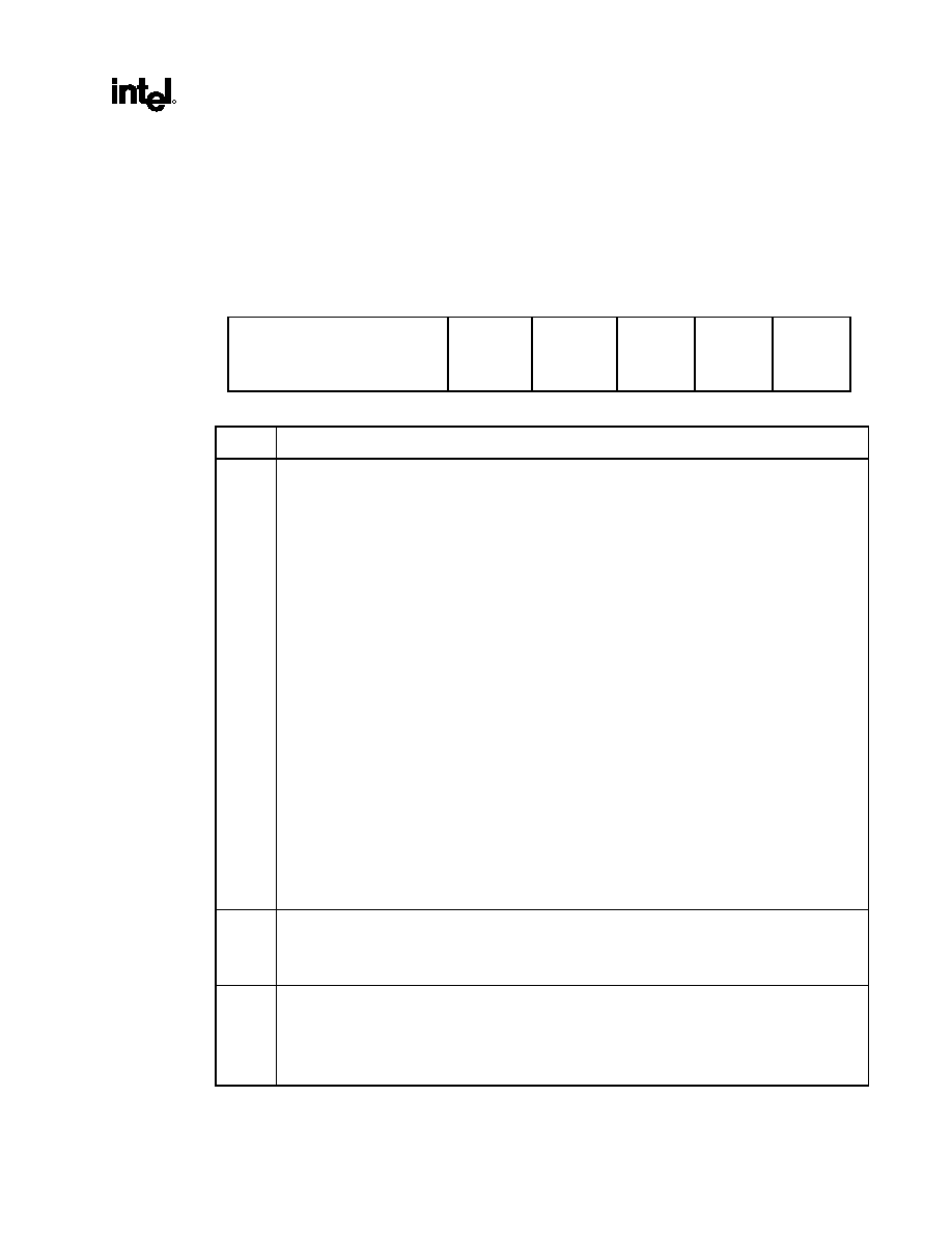
82815EP and 82815P MCH
R
Datasheet
49
3.4.17. DRAMT--DRAM Timing Register (Device 0)
Address Offset:
53h
Default Value:
00h
Access: Read/Write
Size: 8
bits
This register controls the operating mode and the timing of the DRAM Controller.
7
5
4 3 2 1 0
SDRAM Mode Select
DRAM
Cycle Time
Host
Aperture
Cycle
Queue Slot
CAS#
Latency
SDRAM
RAS# to
CAS# Dly
SDRAM
RAS#
Precharge
Bit Description
7:5
SDRAM Mode Select (SMS). These bits select the operational mode of the MCH DRAM interface. The
special modes are intended for initialization at power up.
000 = DRAM in Self-Refresh Mode, Refresh Disabled (Default)
001 = Normal Operation, 100 MHz System memory ≠ Refresh interval 15.6 uSec
133 MHz System memory ≠ Refresh interval 11.7 uSec
010 = Normal Operation, 100 MHz System memory ≠ Refresh interval 7.8
133 MHz System memory ≠ Refresh interval 5.85 uSec
011 = Normal Operation, 100 MHz System memory ≠ Refresh interval 1.28 uSec
133 MHz System memory ≠ Refresh interval 0.96 uSec
100 = NOP Command Enable. In this mode all processor cycles to SDRAM result in a NOP
Command on the SDRAM interface.
101 = All Banks Precharge Enable. In this mode all processor cycles to SDRAM result in an All
Banks Precharge Command on the SDRAM interface.
110 = Mode Register Set Enable. In this mode all processor cycles to SDRAM result in a mode
register set command on the SDRAM interface. The Command is driven on the MA[12:0] lines.
MA[2:0] must always be driven to 010 for burst of 4 mode. MA3 must be driven to 1 for
interleave wrap type. MA4 needs to be driven to the value programmed in the CAS# Latency bit.
MA[6:5] should always be driven to 01. MA[12:7] must be driven to 00000. BIOS must calculate
and drive the correct host address for each row of memory such that the correct command is
driven on the MA[12:0] lines.
Note that MAB[7:4]# are inverted from MAA[7:4]; BIOS must account for this.
111 = CBR Enable. In this mode all processor cycles to SDRAM result in a CBR cycle on the SDRAM
interface.
4
DRAM Cycle Time (DCT). This bit controls the number of SCLKs for an access cycle.
0 = Tras = 5 SCLKs and Trc = 7 SCLKs (Default)
1 = Tras = 7 SCLKs and Trc = 9 SCLKs.
3
Host Aperture Cycle Queue Slot
0 = Default value. No dedicated queue slot is reserved for host to aperture cycles.
1 = A dedicated queue slot is reserved for host to aperture cycles.
The BIOS should set this bit to `1'.
82815EP and 82815P MCH
R
50
Datasheet
Bit Description
2
CAS# Latency (CL). This bit controls the number of CLKs between when a read command is sampled
by the SDRAMs and when MCH samples read data from the SDRAMs.
0 = CAS# latency is 3 SCLKs.
1 = CAS# latency is 2 SCLKs.
1
SDRAM RAS# to CAS# Delay (SRCD). This bit controls the number of SCLKs from a Row Activate
command to a read or write command.
0 = 3 clocks are inserted between a row activate command and either a read or write command.
1 = 2 clocks are inserted between a row activate and either a read or write command.
0
SDRAM RAS# Precharge (SRP). This bit controls the number of SCLKs for RAS# precharge.
0 = 3 clocks of RAS# precharge are provided.
1 = 2 clocks of RAS# precharge are provided
3.4.18. DRP2--DRAM Row Population Register 2 (Device 0)
Address Offset:
54h
Default Value:
00h
Access:
Read/Write (Read-Only if D_LCK = 1)
Size: 8
bits
This register extends support to 6 physical rows of DRAM in 3 DIMMs. The width of a row is 64 bits.
This second DRAM Row Population Register (DRP2) defines the population of each side of DIMM 2.
Note that this entire register becomes read-only when the D_LCK bit is set. For D_LCK bit description,
see SMRAM register (Device 0, address offset 70h).
If the system memory interface is configured to run at 133 MHz, the system BIOS must use the DRP
register (offset 52h) along with the DRP2 register (offset 52h) to detect whether the memory
configuration exceeds 2 double-sided DIMMs or 3 single-sided DIMMs. If so, the system BIOS must
down-shift the clock generator to 100 MHz to guarantee electrical integrity and timings.
7
4
3
0
Reserved DIMM
2
Population
Bit Description
7:4 Reserved.
3:0
DIMM 2 Population. This field indicates the population of DIMM 2. Refer to the Supported System
Memory DIMM Configurations table located with the DRP register definition. Note that some of the
larger capacity DIMMs may not be supported in DIMM 2 based on the capacities of DIMM 0 and
DIMM 1. The maximum supported main memory capacity is 512 MB.

82815EP and 82815P MCH
R
Datasheet
51
3.4.19. FDHC--Fixed DRAM Hole Control Register (Device 0)
Address Offset:
58h
Default Value:
00h
Access: Read/Write
Size: 8
bits
This 8-bit register controls a single fixed DRAM hole: 15 MB≠16 MB.
7 6
0
Hole EN
Reserved
Bit Description
7
Hole Enable (HEN). This field enables a memory hole in DRAM space. Host cycles matching an
enabled hole are passed on to the I/O Controller Hub through the hub interface. Hub interface and PCI
cycles matching an enabled hole are ignored by the MCH. Note that a selected hole is not re-mapped.
0 = No Hole Enabled
1 = 15 MB≠16 MB (1MB) Hole Enabled
6:0 Reserved.
3.4.20. PAM--Programmable Attributes Map Registers (Device 0)
Address Offset:
59≠5Fh
Default Value:
00h
Attribute: Read/Write
Size: 4
bits/register
The MCH allows programmable memory attributes on 13 Legacy memory segments of various sizes in
the 640 KB to 1 MB address range. Seven Programmable Attribute Map (PAM) Registers are used to
support these features. Cacheability of these areas is controlled via the MTRR registers in the P6
processor. Two bits are used to specify memory attributes for each memory segment. These bits apply to
both host, AGP/PCI, and hub interface initiator accesses to the PAM areas. These attributes are:
∑
Read Enable (RE). When RE = 1, the processor read accesses to the corresponding memory
segment are claimed by the MCH and directed to main memory. Conversely, when RE = 0, the host
read accesses are directed to the hub interface/PCI0.
∑
Write Enable (WE). When WE = 1, the host write accesses to the corresponding memory segment
are claimed by the MCH and directed to main memory. Conversely, when WE = 0, the host write
accesses are directed to the hub interface/PCI0.
The RE and WE attributes permit a memory segment to be Read-Only, Write Only, Read/Write, or
disabled. For example, if a memory segment has RE = 1 and WE = 0, the segment is Read-Only.
Each PAM Register controls two regions, typically 16 KB in size. Each of these regions has a 4-bit field.
The four bits that control each region have the same encoding and are defined in the following table.

82815EP and 82815P MCH
R
52
Datasheet
Table 4. Attribute Bit Assignments
Bits [7, 3]
Reserved
Bits [6, 2]
Reserved
Bits [5, 1]
WE
Bits [4, 0]
RE
Description
X X 0 0
Disabled. DRAM is disabled and all accesses
are directed to the hub interface. The MCH
does not respond as a AGP/PCI or hub
interface target for any read or write access to
this area.
X X 0 1
Read-Only. Reads are forwarded to DRAM
and writes are forwarded to the hub interface
for termination. This write protects the
corresponding memory segment. The MCH
responds as a AGP/PCI or hub interface
target for read accesses but not for any write
accesses.
X X 1 0
Write Only. Writes are forwarded to DRAM
and reads are forwarded to the hub interface
for termination. The MCH responds as a
AGP/PCI or hub interface target for write
accesses but not for any read accesses.
X X 1 1
Read/Write. This is the normal operating
mode of main memory. Both read and write
cycles from the host are claimed by the MCH
and forwarded to DRAM. The MCH responds
as a AGP/PCI or hub interface target for both
read and write accesses.
As an example, consider a BIOS that is implemented on the expansion bus. During the initialization
process, BIOS can be shadowed in main memory to increase the system performance. When BIOS is
shadowed in main memory, it should be copied to the same address location. To shadow the BIOS, the
attributes for that address range should be set to write only. BIOS is shadowed by first doing a read of
that address. This read is forwarded to the expansion bus. The host then does a write of the same address,
which is directed to main memory. After BIOS is shadowed, the attributes for that memory area are set to
read-only so that all writes are forwarded to the expansion bus. The table above and the figure below
show the PAM registers and the associated attribute bits.
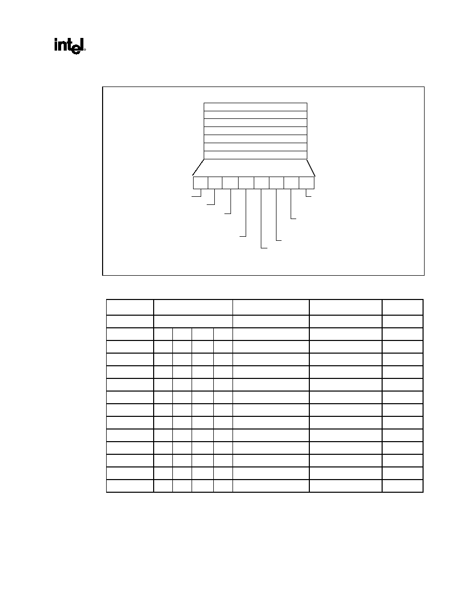
82815EP and 82815P MCH
R
Datasheet
53
Figure 3. PAM Registers
pam
RE
WE
RE
R
R
WE
R
R
7
6
5
4
3
2
1
0
PAM6
PAM5
PAM4
PAM3
PAM2
PAM1
PAM0
Read Enable (R/W
1=Enable
0=Disable
Write Enable (R/W)
1=Enable
0=Disable
Reserved
Reserved
Read Enable (R/W)
1=Enable
0=Disable
Write Enable (R/W)
1=Enable
0=Disable
Reserved
Reserved
5Fh
5Eh
5Dh
5Ch
5Bh
5Ah
59h
Offset
Table 5. PAM Registers and Associated Memory Segments
PAM Reg
Attribute Bits
Memory Segment
Comments
Offset
PAM0[3:0] Reserved
59h
PAM0[7:4] R
R
WE
RE
0F0000h≠0FFFFFh BIOS
Area
59h
PAM1[3:0]
R
R
WE
RE
0C0000h≠0C3FFFh
ISA Add-on BIOS
5Ah
PAM1[7:4] R
R
WE
RE
0C4000h≠0C7FFFh ISA
Add-on
BIOS
5Ah
PAM2[3:0]
R
R
WE
RE
0C8000h≠0CBFFFh
ISA Add-on BIOS
5Bh
PAM2[7:4]
R
R
WE
RE
0CC000h≠ 0CFFFFh
ISA Add-on BIOS
5Bh
PAM3[3:0]
R
R
WE
RE
0D0000h≠ 0D3FFFh
ISA Add-on BIOS
5Ch
PAM3[7:4]
R
R
WE
RE
0D4000h≠ 0D7FFFh
ISA Add-on BIOS
5Ch
PAM4[3:0]
R
R
WE
RE
0D8000h≠ 0DBFFFh
ISA Add-on BIOS
5Dh
PAM4[7:4]
R
R
WE
RE
0DC000h≠ 0DFFFFh
ISA Add-on BIOS
5Dh
PAM5[3:0]
R
R
WE
RE
0E0000h≠ 0E3FFFh
BIOS Extension
5Eh
PAM5[7:4]
R
R
WE
RE
0E4000h≠ 0E7FFFh
BIOS Extension
5Eh
PAM6[3:0]
R
R
WE
RE
0E8000h≠ 0EBFFFh
BIOS Extension
5Fh
PAM6[7:4]
R
R
WE
RE
0EC000h≠ 0EFFFFh
BIOS Extension
5Fh

82815EP and 82815P MCH
R
54
Datasheet
DOS Area (00000h≠9FFFFh)
The DOS area is 640 KB in size is always mapped to the main memory controlled by the MCH.
Video Buffer Area (A0000h≠BFFFFh)
The 128 KB graphics adapter memory region is normally mapped to a legacy video device on the hub
interface/PCI (typically VGA controller). This area is not controlled by attribute bits and processor ≠
initiated cycles in this region are forwarded to either the hub interface or the AGP/Internal Graphics
Device for termination. This region is also the default region for SMM space.
Accesses to this range are directed to either the hub interface or the AGP/internal Graphics Device based
on the configuration. The configuration is specified by:
1. AGP on/off configuration bit
2. AGP off: GMS bits of the SMRAM register in the MCH Device 0 configuration space. There is
additional steering information coming from the Device 2* configuration registers and from some
of the VGA registers in the Graphics device.
3. AGP on: MCHCFG (Device 0, bit 5, PCI-PCI Command) and BCTRL (Device 1, bit 3, PCI-PCI
Bridge Control) configuration registers
Control is applied for accesses initiated from any of the system interfaces; that is, processor bus, the hub
interface, or AGP (if enabled). Note that for the hub interface to AGP/PCI accesses, only memory write
operations are supported. Any AGP/PCI initiated VGA accesses targeting the MCH will master abort.
For more details, see the descriptions in the configuration registers specified above.
The SMRAM Control register controls how SMM accesses to this space are treated.
Monochrome Adapter (MDA) Range (B0000h≠B7FFFh)
Legacy support requires the ability to have a second graphics controller (monochrome) in the system.
In an AGP system, accesses in the standard VGA range are forwarded to the AGP bus (depending on
configuration bits). Since the monochrome adapter may be on the hub interface/PCI (or ISA) bus, the
MCH must decode cycles in the MDA range and forward them to the hub interface. This capability is
controlled by a configuration bit (MDA bit ≠ Device 0, BEh). In addition to the memory range B0000h
to B7FFFh, the MCH decodes I/O cycles at 3B4h, 3B5h, 3B8h, 3B9h, 3Bah and 3BFh and forwards
them to the hub interface.
In an internal graphics system, the GMS bits of the SMRAM register in Device 0, bits in the Device 2
PCICMD register, and bits from some of the VGA registers control this functionality.

82815EP and 82815P MCH
R
Datasheet
55
Expansion Area (C0000h≠DFFFFh)
This 128 KB ISA Expansion region is divided into eight 16 KB segments. Each segment can be assigned
one of four Read/Write states: read-only, write-only, read/write, or disabled. Typically, these blocks are
mapped through MCH and are subtractively decoded to ISA space. Memory that is disabled is not
remapped.
Extended System BIOS Area (E0000h≠EFFFFh)
This 64 KB area is divided into four 16 KB segments. Each segment can be assigned independent read
and write attributes so it can be mapped either to main DRAM or to the hub interface. Typically, this area
is used for RAM or ROM. Memory segments that are disabled are not remapped elsewhere.
System BIOS Area (F0000h≠FFFFFh)
This area is a single 64 KB segment. This segment can be assigned read and write attributes. It is by
default (after reset) read/write disabled and cycles are forwarded to the hub interface. By manipulating
the read/write attributes, the MCH can "shadow" BIOS into the main DRAM. When disabled, this
segment is not remapped.
82815EP and 82815P MCH
R
56
Datasheet
3.4.21. SMRAM--System Management RAM Control Register
(Device 0)
Address Offset:
70h
Default Value:
00h
Access: Read/Write,
Read-Only
Size: 8
bits
The SMRAM register controls how accesses to Compatible and Extended SMRAM spaces are treated,
and how much (if any) memory is "Stolen" from the system to support both SMRAM and graphics local
memory needs.
7 6
5 4
3 2
1
0
Graphics Mode Select
Upper SMM Select
Lower SMM Select
SMM
Space
Locked
E_SMRA
M_ERR
Bit Description
7:6
Graphics Mode Select (GMS). This field is used to enable/disable the Internal Graphics device and
select the amount of main memory that is "Stolen" to support the internal graphics device in VGA (non-
linear) mode only. These 2 bits only have meaning if we are not in AGP mode.
00 = Internal graphics device Disabled, No memory "Stolen"
01 = Internal graphics device Enabled, No memory "Stolen"
10 = Internal graphics device Enabled, 512 KB of memory "Stolen" for frame buffer.
11 = Internal graphics device Enabled, 1 MB of memory "Stolen" for frame buffer.
Notes:
∑
When the internal graphics device is disabled (00), the graphics device and all of its memory and I/O
functions are disabled and the clocks to this logic are turned off; memory accesses to the VGA range
(A0000≠BFFFF) are forwarded on to the hub interface and the graphics local memory space is NOT
"stolen" from main memory. Any change to the SMRAM register will not affect AGP mode or cause
the controller to go into AGP mode. When this field is non-zero, the internal graphics device and all of
its memory and I/O functions are enabled; all non-SMM memory accesses to the VGA range will be
handled internally and the selected amount of graphics local memory space (0, 512 KB or 1 MB) is
"stolen" from the main memory. Graphics memory is "stolen" AFTER TSEG memory is "stolen".
∑
Once D_LCK is set, these bits becomes read-only.
∑
MCH does not support VGA on local memory. Software must not use the 01 mode for VGA.

82815EP and 82815P MCH
R
Datasheet
57
Bit Description
5:4
Upper SMM Select (USMM). This field is used to enable/disable the various SMM memory ranges
above 1 MB. TSEG is a block of memory ("Stolen" from Main Memory at [TOM-Size] : [TOM]) that is
only accessable by the processor and only while operating in SMM mode. HSEG is a remap of the AB
segment at FEEA0000 : FEEBFFFF. Both of these areas, when enabled, are usable as SMM RAM.
00 = TSEG and HSEG are both disabled
01 = TSEG is disabled, HSEG is conditionally enabled
10 = TSEG is enabled as 512 KB and HSEG is conditionally enabled
11 = TSEG is enabled as 1 MB and HSEG is conditionally enabled
Note:
∑
Non-SMM Operations (SMM processor accesses and all other access) that use these address ranges
are forwarded to the hub interface.
∑
Once D_LCK is set, these bits becomes read-only.
∑
HSEG is ONLY enabled if LSMM = 00.
3:2
Lower SMM Select (LSMM). This field controls the definition of the AB segment SMM space.
00 = AB segment disabled (no one can write to it).
01 = AB segment enabled as general system RAM (anyone can write to it).
10 = AB segment enabled as SMM Code RAM shadow. Only SMM code reads can access DRAM in the
AB segment (processor code reads only). SMM Data operations and all Non-SMM Operations go
to either the internal graphics device or are broadcast on the hub interface.
11 = AB segment enabled as SMM RAM. All SMM operations to the AB segment are serviced by
DRAM, all Non-SMM operations go to either the internal graphics device or are broadcast on the
hub interface (processor SMM R/W can access SMM space).
When D_LCK is set, bit 3 becomes read-only, and bit 2 is writable ONLY if bit 3 is a 1. When bit 3 is set,
only the processor can access it.
1
SMM Space Locked (D_LCK). When D_LCK is set to 1 then D_LCK, GMS, USMM, and the most
significant bit of LSMM become read-only. D_LCK can be set to 1 via a normal configuration space write
but can only be cleared by a reset. The combination of D_LCK and LSMM provide convenience with
security. The BIOS can use LSMM=01 to initialize SMM space and then use D_LCK to "lock down"
SMM space in the future so that no application software (or BIOS itself) can violate the integrity of SMM
space, even if the program has knowledge of the LSMM function. This bit also Locks the DRP and
DRP2 registers.
0
E_SMRAM_ERR (E_SMERR).
1 = This bit is set when processor accesses the defined memory ranges in Extended SMRAM (HSEG or
TSEG) while not in SMM mode. This bit is Not set for the case of an explicit write-back operation.
0 = It is software's responsibility to clear this bit. Software must write a 1 to this bit to clear it.
82815EP and 82815P MCH
R
58
Datasheet
3.4.22. MISCC--Miscellaneous Control Register (Device 0)
Address Offset:
72≠73h
Default Value:
0000h
Access: Read/Write,
Read-Only
Size: 16
bits
This register holds all of the miscellaneous control bits for the MCH .
15 14
12 11 10
8
SM GFX
133
Enable
Reserved CPC
Mask Reserved
7
6
5
4
3 2 1 0
Read PWR Throttle Cntl
Write PWR Throttle Cntl
Throttle
Lock
Reserved BNR
Looka
head
GFX LM
Win Size
Sel
Bit Description
15
System Memory Graphics PC133 Enable--R/W. This bit allows the MCH to operate in Graphics
Mode with Enhanced System Memory (PC133). Normally, SM frequency is locked to 100 MHz in
Internal Graphics mode, and MCHCFG[2] (SMFS) is read-only. Setting this bit allows the SM frequency
to be changed by writing to MCHCFG[2]. This bit has no effect in AGP mode.
0 = Normal Operation. MCHCFG[2] hardwired to 0 when MCH is in Graphics Mode
(i.e., APCONT[0] = 1)
1 = Allow 133 MHz System Memory when the MCH is in Graphics Mode. Note that this just enables
PC133. To actually run graphics with 133 MHz SM, MCHCFG[2] must be set to 1. Also, this bit
should be set by BIOS before MCH is changed from AGP to Graphics mode via APCONT[0].
14 Reserved.
13
SM Transmit Stage Bypass--R/W.
0 = Normal Operation (Default). Bypass if SM=100 MHz; No bypass if SM=133 MHz.
1 = Always bypass, regardless of SM frequency.
System BIOS should set this bit to 1 to enable the bypass and optimize system memory latency by one
clock for 133 MHz operation (has no affect on 100 MHz operation).
12 Reserved.
11
CPC Mask Enable--R/W.
0 = Normal Operation (default).
1 = Never perform command per clock accesses to system memory. Mask command per clock.
Note: This bit must be set to 1 if using 133 MHz system memory.
10:8 Reserved.

82815EP and 82815P MCH
R
Datasheet
59
Bit Description
7:6
Read Power Throttle Control--R/W. These bits select the Power Throttle Bandwidth Limits for read
operations to system memory.
R/W, RO if Throttle Lock (bit 3 =1). These bits are locked (read-only) when bit 3 (Throttle Lock) is 1.
00 = No Limit
(800 MB/Sec) (Default)
01 = Limit at 87 Ω %
(700 MB/Sec)
10 = Limit at 75 %
(600 MB/Sec)
11 = Limit at 62 Ω %
(500 MB/Sec)
5:4
Write Power Throttle Control--R/W. These bits select the Power Throttle Bandwidth Limits for Write
operations to System Memory.
R/W, RO if Throttle Lock (bit 3 =1). These bits are locked (read-only) when bit 3 (Throttle Lock) is 1.
00 = No Limit
(800 MB/Sec) (Default)
01 = Limit at 62 Ω % ( 500 MB/Sec)
10 = Limit at 50 %
( 400 MB/Sec)
11 = Limit at 37 Ω % ( 300 MB/Sec)
Note: These bits must be set to `01' if using 100 MHz system memory and `10' if using 133 MHz
system memory.
3
Throttle Lock--R/W.
R/W, RO if Throttle Lock (bit 3 =1). Once set, this bit can only be cleared by a reset.
0 = Bits [7:3] remain writeable
1 = Block writes to bits [7:3]
2 Reserved--RO.
1
BNR Lookahead--R/W. This enables the HT unit to look further up the data path to optimize the BNR
(Block New Requests) signal to increase our effective IOQ (In Order Queue) depth.
0 = Normal Behavior (default)
1 = BNR Lookahead Enable
0
Graphics Translation Window Size Select--R/W. In GFX mode this would be the size of the GTT
(Graphics Translation Table). Not a valid bit in AGP mode.
0 = 64 MB (default)
1 = 32 MB.
82815EP and 82815P MCH
R
60
Datasheet
3.4.23. CAPID--Capability Identification (Device 0: AGP Mode Only)
Address Offset:
88≠8Bh
Default Value:
F104 A009h
Access: Read-Only
Size: 32
bits
This register
uniquely identifies chipset capabilities as defined in the table below. Writes to this register have no
effect.
31 30 29 28
27
24
133 MHz
Capability
Display
Cache
Capability
AGP
Capability
Internal
Graphics
Capability
CAPID Version
23
16
CAPID Length
15
8
Next Capability Pointer
7
0
CAP_ID
Bit Description
31
133 MHz Capability--RO.
0 = Component is capable of up to 100 MHz front side bus and system memory.
1 = Component is capable of up to 133 MHz front side bus and system memory.
30
Display Cache Capability--RO.
0 = Only supports UMA mode (no local memory).
1 = Component is local memory (Display Cache) and UMA capable.
29
AGP Capability--RO.
0 = AGP mode not supported. Note that the AGP interface may still be active through the addition of
an AIMM card if bits 28 and 30 are both 1.
1 = AGP mode supported.
28
Internal Graphics Capability--RO.
0 = Internal graphic controller not supported.
1 = Internal graphic controller supported.
27:24
CAPID Version--RO. This field has the value 0001b to identify the first revision of the CAPID register
definition.
23:16
CAPID Length--RO. This field has the value 04h to indicate the structure length.
82815EP and 82815P MCH
R
Datasheet
61
Bit Description
15:8
Next Capability Pointer--RO. This field has two possible values based on APCONT[0] at offset 51h:
A0h when APCONT[0] = 0 (AGP Mode) meaning the next capability pointer is ACAPID.
00h when APCONT[0] = 1 (GFX Mode) meaning that this was the last capability pointer in the list.
7:0
CAP_ID--RO. This field has the value 1001b to identify the CAP_ID assigned by the PCI SIG for
vendor dependent capability pointers.
3.4.24. BUFF_SC--System Memory Buffer Strength Control Register
(Device 0)
Address Offset:
92≠93h
Default Value:
FFFFh
Access: Read/Write
Size: 16
bits
This register programs the system memory DRAM interface signal buffer strengths, with the exception of
the CKEs. The programming of these bits should be based on DRAM density (x8 or x16), DRAM
technology (16Mb, 64Mb, 128Mb or 256 Mb), rows populated, etc.. Note that x4 & x32 DRAMs are not
supported. Registered DIMMs and DIMMS with ECC are also not supported and BIOS upon detection
of ECC via SPD, should report to the user that ECC DIMM timings are not supported by the MCH.
In the descriptions below, the term "Row" is equivalent to one side of one DIMM. In other words, a
"single-sided" DIMM contains one populated row (always an odd numbered), and one empty row (even
numbered). A "double-sided" DIMM contains two populated rows.
All buffer strengths are based on the number of "loads" connected to each pin of a given signal group. A
"load" represents one pin of one SDRAM Device. The MCH pin is implied and not counted in the load
equations. The number of loads on a given signal for a given configuration can be determined entirely
from the width of the SDRAM devices that populate each row in the configuration. This information is
readily available for each row via the Serial Presence Detect mechanism.
Regardless of system memory interface frequency, the SMAA [11:8, 3:0], SBS [1:0] SWE#, SCAS#, and
SRAS# signal buffer strengths for all rows should be set accordingly to the DIMM loading which is
defined by bits [1:0] in the table below.
15 14 13 12 11 10
9
8
SCS[5]#
Buffer
Strength
SCS[4]#
Buffer
Strength
SCS[3]#
Buffer
Strength
SCS[2]#
Buffer
Strength
SCS[1]#
Buffer
Strength
SCS[0]#
Buffer
Strength
SMAC[7:4]# Buffer
Strength
7 6
5 4
3 2
1 0
SMAB[7:4]# Buffer
Strength
SMAA[7:4] Buffer
Strength
MD and DQM Buffer
Strengths
Control Buffer Strengths

82815EP and 82815P MCH
R
62
Datasheet
Bit Description
15
SCS[5]# Buffer Strength (Row 5).
0 = Reserved
1 = 1.0x 0 or 2 load or 4 loads
Each Row is actually selected by a pair of chip select signals (SCSA[n]# and SCSB[n]#). The number of
SCS# loads for a given row can be determined from SPD data using the following equation:
Loads = 32 / (width of SDRAM devices in row)
14
SCS[4]# Buffer Strength (Row 4).
0 = Reserved
1 = 1.0x 0 or 2 load or 4 loads
13
SCS[3]# Buffer Strength (Row 3).
0 = Reserved
1 = 1.0x 0 or 2 load or 4 loads
12
SCS[2]# Buffer Strength (Row 2).
0 = Reserved
1 = 1.0x 0 or 2 load or 4 loads
11
SCS[1]# Buffer Strength (Row 1).
0 = Reserved
1 = 1.0x 0 or 2 load or 4 loads
10
SCS[0]# Buffer Strength (Row 0).
0 = Reserved
1 = 1.0x 0 or 2 load or 4 loads
9:8
SMAC[7:4]# Buffer Strength (Rows 4/5).
00 = 2.7x > 8 loads
01 = 1.7x 8 loads
10 = 1.0x 0 or 4 loads
11 = 1.0x 0 or 4 loads
Separate copies of these SMA*[7:4] "Command-Per-Clock" signals are provided for each DIMM. So the
loads for each copy are determined by the number of SDRAM devices on the corresponding DIMM (4, 8,
12, or 16 loads). The number of loads for each SMA*[7:4] signal group can be determined from SPD
data using the following equation:
Loads = (64 / (SDRAM Device Width for 1
st
row)) + (64 / (SDRAM Device Width for 2
nd
row))
7:6
SMAB[7:4]# Buffer Strength (Rows 2/3).
00 = 2.7x > 8 loads
01 = 1.7x 8 loads
10 = 1.0x 0 or 4 loads
11 = 1.0x 0 or 4 loads

82815EP and 82815P MCH
R
Datasheet
63
Bit Description
5:4
SMAA[7:4] Buffer Strength (Rows 0/1).
00 = 2.7x > 8 loads
01 = 1.7x 8 loads
10 = 1.0x 0 or 4 loads
11 = 1.0x 0 or 4 loads
3:2
SMD[63:0] and SDQM[7:0] Buffer Strengths (All Rows).
00 = Reserved (1.7x)
01 = Reserved (0.7x)
10 = Reserved (1.0x)
11 = 1.0x 1-6 loads
The load on the SMD and SDQM signals is a function only of the number of populated rows in the
system (range 1 to 6 loads):
Loads = Number of populated rows.
1:0
SWE#, SCAS#, SRAS#, SMAA[11:8, 3:0], SBS[1:0] Control Buffer Strengths (All Rows).
00 = 1.7x > 32 loads
01 = 0.7x < 8 loads
10 = 1.0x 8-32 loads
11 = 1.0x 8-32 loads
The load on the address and control signals (other than SMA*[7:4] above) is simply the number of
devices populated in ALL rows (range from 4 to 48 loads!).
Loads = (64 / Row 0 Device Width) + (64 / Row 1 Device Width) + (64 / Row 2 Device Width) +
(64 / Row 3 Device Width) + (64 / Row 4 Device Width) + (64 / Row 5 Device Width)
82815EP and 82815P MCH
R
64
Datasheet
3.4.25. BUFF_SC2--System Memory Buffer Strength Control Register
2 (Device 0)
Address Offset:
94≠95h
Default Value:
FFFFh
Access: Read/Write
Size: 16
bits
This register programs the system memory DRAM interface CKE signal buffer strengths. See BUFF_SC
register for the remainder of the buffer strength controls.
15
8
Reserved (R/W)
7
6
5 4 3 2 1 0
Reserved (R/W)
CKE5
Buffer
Strength
CKE4
Buffer
Strength
CKE3
Buffer
Strength
CKE2
Buffer
Strength
CKE1
Buffer
Strength
CKE0
Buffer
Strength
Bit Description
15:6 Reserved.
5
SCKE[5] Buffer Strength (Row 5).
0 = 2.7x 8 loads
1 = 1.7x 0 or 4 loads
The load on a given SCKE signal is equal to the number of SDRAM devices for that particular row
(either 4 or 8 loads).
Loads = (64 / SDRAM Device Width for this row)
4
SCKE[4] Buffer Strength (Row 4).
0 = 2.7x 8 loads
1 = 1.7x 0 or 4 loads
3
SCKE[3] Buffer Strength (Row 3).
0 = 2.7x 8 loads
1 = 1.7x 0 or 4 loads
2
SCKE[2] Buffer Strength (Row 2).
0 = 2.7x 8 loads
1 = 1.7x 0 or 4 loads
1
SCKE[1] Buffer Strength (Row 1).
0 = 2.7x 8 loads
1 = 1.7x 0 or 4 loads
0
SCKE[0] Buffer Strength (Row 0).
0 = 2.7x 8 loads
1 = 1.7x 0 or 4 loads
82815EP and 82815P MCH
R
Datasheet
65
3.4.26. SM_RCOMP--System Memory R Compensation Control
Register (Device 0)
Address Offset:
98≠9Bh
Default Value:
XXXXXXXXh
Access: Read/Write,
Read-Only
Size: 32
bits
This register controls the system memory Rcomp buffers (both horizontally and vertically oriented).
31 30
23
22
20 19 18
16
V Override
Enable
Reserved SRCOMP_VP
Reserved
SRCOMP_VN
15 14
7
6
4 3 2
0
H Override
Enable
Reserved SRCOMP_HP
Reserved
SRCOMP_HN
Bit Description
31
SRCOMP_V Override Enable--R/W.
0 = SM Rcomp is active for vertically oriented buffers (Default).
1 = SM Rcomp is NOT-active for vertically oriented buffers.
30:23 Reserved.
22:20
SRCOMP_VP--RO or R/W. P-Channel Compensation Value for Vertical Buffers. This value is
generated by the Rcomp logic to control the drive characteristics of the vertically oriented P-channel
devices in the SM buffers.
In Normal operation, field is read-only and reflects current compensation.
In Override Mode (see bit 31), field is written with desired compensation value which is loaded via
software when SM Rcomp operation is disabled.
19 Reserved.
18:16
SRCOMP_VN--RO or R/W. N-Channel Compensation Value for Vertical Buffers. This value is
generated by the Rcomp logic to control the drive characteristics of the vertically oriented N-channel
devices in the SM buffers.
In Normal operation, field is read-only and reflects current compensation.
In Override Mode (see bit 31), field is written with desired compensation value which is loaded via
software when SM Rcomp operation is disabled.
15
SRCOMP_H Override Enable--R/W.
0 = SM Rcomp is active for horizontally oriented buffers (Default).
1 = SM Rcomp is NOT-active for horizontally oriented buffers.
14:7 Reserved.
82815EP and 82815P MCH
R
66
Datasheet
Bit Description
6:4
SRCOMP_HP--RO or R/W. P-Channel Compensation Value for Horizontal Buffers. This value is
generated by the Rcomp logic to control the drive characteristics of the horizontally oriented P-channel
devices in the SM buffers.
In Normal operation, field is read-only and reflects current compensation.
In Override Mode (see bit 15), field is written with desired compensation value which is loaded via
software when SM Rcomp operation is disabled.
3 Reserved.
2:0
SRCOMP_HN--RO or R/W. N-Channel Compensation Value for Horizontal Buffers. This value is
generated by the Rcomp logic to control the drive characteristics of the horizontally oriented N-channel
devices in the SM buffers.
In Normal operation, field is read-only and reflects current compensation.
In Override Mode (see bit 15), field is written with desired compensation value which is loaded via
software when SM Rcomp operation is disabled.
3.4.27. SM--System Memory Control Register
Address Offset:
9C≠9Fh
Default Value:
XXXXXXXXh
Access: Read/Write,
Read-Only
Size: 32
bits
This register controls the two System Memory Delay Locked Loop (DLL) blocks that offset the transmit
and receive clocks used to interface with the external SDRAM devices. The Transmit DLL provides an
early version of SCLK to provide additional setup margin to the external SDRAM devices. The Receive
DLL provides a late version of SCLK to provide additional setup time on read data driven by the
SDRAM devices back to the MCH.
By default, the Transmit DLL is enabled (whether the operating frequency is 100 MHz or 133 MHz).
The Receive DLL is always bypassed, regardless of operating frequency. When the RDLL is bypassed,
the RDLL Bias field, instead, controls a buffer delay chain with programmable tap points. This chain has
8 tap points each with approximately 200 ps of incremental delay at the slow corner (total delay range
0 to 1.4 ns) and about 80 ps of incremental delay at the "fast" corner (0 to 0.56 ns total range).
31
16
15
14
0
Reserved TDLL
Bypass
Reserved
Bit Description
31:16 Reserved.
15
Transmit DLL Enable (TDLLE)--R/W.
0 = TDLL Enabled (Default)
1 = TDLL Disabled and bypassed
14:0 Reserved.
82815EP and 82815P MCH
R
Datasheet
67
3.4.28. ACAPID--AGP Capability Identifier Register
(Device 0: AGP Mode Only)
Address Offset:
A0≠A3h
Default Value:
00200002h
Access: Read-Only
Size: 32
bits
This register provides standard identifier for AGP capability.
31
24
Reserved
23
20
19
16
Major AGP Revision Number
Minor AGP Revision Number
15
8
Next Capability Pointer
7
0
AGP Capability ID
Bit Description
31:24 Reserved.
23:20
Major AGP Revision Number. These bits provide a major revision number of AGP specification that
this version of MCH conforms. These bits are set to the value 0010b to indicate AGP Rev. 2.x.
19:16
Minor AGP Revision Number. These bits provide a minor revision number of AGP specification that
this version of MCH conforms. This number is hardwired to a value of "0000" (i.e., implying Rev x.0).
Together with major revision number this field identifies MCH as an AGP REV 2.0 compliant device.
15:8
Next Capability Pointer. AGP capability is the first and the last capability described via the capability
pointer mechanism; therefore, these bits are hardwired to 0s to indicate the end of the capability linked
list.
7:0
AGP Capability ID. This field identifies the linked list item as containing AGP registers. This field has
the value 0000_0010b as assigned by the PCI SIG.
82815EP and 82815P MCH
R
68
Datasheet
3.4.29. AGPSTAT--AGP Status Register (Device 0: AGP Mode Only)
Address Offset:
A4≠A7h
Default Value:
1F000207h
Access: Read-Only
Size: 32
bits
This register reports AGP device capability/status.
31
24
Request Queue (RQ) (HW=1Fh)
23
16
Reserved
15
10
1 8
Reserved SBA
(HW=1)
Reserved
7
6 5
4
3 2
0
Reserved >4
GB
Support
(HW=0)
Fast
Writes
(HW=0)
Reserved
Data Transfer Rate
(HW=111; 1x,2x,4x modes supported)
Bit Description
31:24
Request Queue (RQ). This field is hardwired to 1Fh to indicate a maximum of 32 outstanding AGP
command requests can be handled by the MCH. This field contains the maximum number of AGP
command requests the MCH is configured to manage. The lower 6 bits of this field reflect the value
programmed in AGPCTRL[12:10]. Only discrete values of 32, 16, 8, 4 , 2 and 1 can be selected via
AGPCTRL. Upper bits are hardwired to 0.
Default =1Fh to allow a maximum of 32 outstanding AGP command requests.
23:10 Reserved
9
SideBand Addressing (SBA). Indicates the MCH supports sideband addressing. Hardwired to 1.
8:6 Reserved
5
Greater Than 4 GB Address Support (4GB). This bit indicates that the MCH does not support
addresses greater than 4 GB. It is hardwired to 0.
4
Fast Writes (FW). This bit indicates that the MCH does not support Fast Writes from the processor to
the AGP master. It is hardwired to a 0.
3 Reserved
2:0
Data Transfer Rate Capability (RATE). After reset the MCH reports its data transfer rate capability.
Note that the selected data transfer mode applies to both AD bus and SBA bus.
Bit 0 = 1 = 1x data transfer mode
Bit 1 = 1 = 2x data transfer mode
Bit 2 = 1 = 4x data transfer mode. This bit can be masked by the AGPCTRL register bit 0
(AGP 4X Override).
1x , 2x , and 4x data transfer modes are supported by the MCH; therefore, this bit field has a Default
Value = 111.
82815EP and 82815P MCH
R
Datasheet
69
3.4.30. AGPCMD--AGP Command Register (Device 0: AGP Mode Only)
Address Offset:
A8≠Abh
Default Value:
00000000h
Access: Read/Write
Size: 32
bits
This register provides control of the AGP operational parameters.
31
10
9 8
Reserved
SBA EN
AGP EN
7
6 5
4
3 2
0
Reserved 4
GB
(HW=0)
FW EN
Reserved
Data Rate
Bit Description
31:10 Reserved.
9
Sideband Address Enable (SBA).
1 = Enable. The sideband addressing mechanism is enabled.
0 = Disable
8
AGP Enable. When this bit is reset to 0, the MCH ignores all AGP operations, including the sync
cycle. Any AGP operations received while this bit is set to 1 will be serviced, even if this bit is reset to
0. If this bit transitions from a 1 to a 0 on a clock edge in the middle of an SBA command being
delivered in 1X mode, the command is issued. When this bit is set to 1 the MCH will respond to AGP
operations delivered via PIPE#, or to operations delivered via SBA, if the AGP Side Band Enable bit is
also set to 1.
7:6 Reserved.
5
Greater Than 4 GB Support (4GB). Hardwired to 0. The MCH as an AGP target does not support
addressing greater than 4 GB.
4
Fast Writes Enable (FW). This bit must always be programmed to 0. The chipset will behave
unpredictably if this bit is programmed with 1.
3 Reserved.
2:0
Data Rate Capability. The settings of these bits determines the AGP data transfer rate. One (and only
one) bit in this field must be set to indicate the desired data transfer rate. The same bit must be set on
both master and target. Configuration software will update this field by setting only one bit that
corresponds to the capability of AGP master (after that capability has been verified by accessing the
same functional register within the AGP master's configuration space.)
Bit 0 = 1= 1X
Bit 1 = 1 = 2X
Bit 2 = 1 = 4x
Bit 2 becomes reserved (but will still read 4x, erroneously) when the 4x Override bit in the AGP CTRL
register is set to 1 because this bit will not be updated in 4x Override mode. When the 4x Override bit
is set writes to Data Rate[2] have no functional impact.
Note: This field applies to AD and SBA buses.

82815EP and 82815P MCH
R
70
Datasheet
3.4.31. AGPCTRL--AGP Control Register (Device 0: AGP Mode Only)
Address Offset:
B0≠B3h
Default Value:
00000000h
Access: Read/Write
Size: 32
bits
This register provides for additional control of the AGP interface.
31
8 7 6
1 0
Reserved GTLB_EN
Reserved
4X
Override
Bit Description
31:8 Reserved
7
GTLB Enable ( and GTLB Flush Control)--R/W.
1 = Enables normal operations of the Graphics Translation Lookaside Buffer.
0 = Disable (default). The GTLB is flushed by clearing the valid bits associated with each entry. In this
mode of operation all accesses that require translation bypass the GTLB. All requests that are
positively decoded to the graphics aperture force the MCH to access the translation table in main
memory before completing the request. Translation table entry fetches are not cached in the GTLB.
NOTE:
∑
When an invalid translation table entry is read, this entry is still cached in the GTLB (ejecting the least
recently used entry).
∑
The MCH flushes the GWB when software sets or clears this bit to ensure coherency between the
GTLB and main memory.
∑
This bit can be changed dynamically (i.e., while an access to GTLB occurs).
6:1 Reserved
0
4X Override. When this bit is set to 1 the Rate[2] bit in the AGPSTAT register will be read as a 0. This
"back-door" register bit allows BIOS to disable AGP 4X mode.
The introduction of universal AGP cards and universal motherboards has raised some potential
problems that this bit alleviates. AGP 2X can operation at 1.5V or 3.3V. AGP 4X can operate only at
1.5V. In a system that is supporting 3.3V operation, and therefore cannot support a 4X transfer
rate, it is the responsibility of the BIOS to make sure that 4X mode is not selected.
82815EP and 82815P MCH
R
Datasheet
71
3.4.32. APSIZE--Aperture Size (Device 0: AGP Mode Only)
Address Offset:
B4h
Default Value:
00h
Access: Read/Write
Size: 8
bits
This register determines the effective size of the graphics aperture used for a particular MCH
configuration. This register can be updated by the MCH-specific BIOS configuration sequence before the
PCI standard bus enumeration sequence takes place. If the register is not updated, a default value will
select an aperture of maximum size (i.e., 64 MB).
7
4
3
2 0
Reserved GFX
Aperture
Size
Reserved
Bit Description
7:4 Reserved.
3
Graphics Aperture Size (GASIZE). Bit 3 operates on bit 25 of the Aperture Base (APBASE)
configuration register. When this bit is 0, it forces bit 25 in APBASE to behave as "hardwired" to 0.
When this bit is 1, it forces bit 25 in APBASE to be read/write accessible. Only the following
combinations are allowed:
0 = 64 MB Aperture Size
1 = 32 MB Aperture Size
Default for APSIZE[3]=0b forces default APBASE[25] =0b (responds as "hardwired" to 0). This provides
maximum aperture size of 64 MB. Programming APSIZE[3]=1b enables APBASE[25] as read/write
programmable.
2:0 Reserved.
82815EP and 82815P MCH
R
72
Datasheet
3.4.33. ATTBASE--Aperture Translation Table Base Register
(Device 0: AGP Mode Only)
Address Offset:
B8≠BBh
Default Value:
00000000h
Access: Read/Write
Size: 32
bits
This register provides the starting address of the Graphics Aperture Translation Table Base located in the
main DRAM. This value is used by the MCH's Graphics Aperture address translation logic (including
the GTLB logic) to obtain the appropriate address translation entry required during the translation of the
aperture address into a corresponding physical DRAM address. The ATTBASE register may be
dynamically changed.
Note: The address provided via ATTBASE is 4 KB aligned.
31 29
28
12
11
0
Reserved ATT
Base
Address
Reserved
Bit Description
31:29 Reserved.
28:12
ATT Base Address. This field contains a pointer to the base of the translation table used to map
memory space addresses in the aperture range to addresses in main memory.
11:0 Reserved.
82815EP and 82815P MCH
R
Datasheet
73
3.4.34. AMTT--AGP Multi-Transaction Timer
(Device 0: AGP Mode Only)
Address Offset:
BCh
Default Value:
00h
Access: Read/Write
Size: 8
bits
AMTT controls the amount of time that the MCH's arbiter allows AGP/PCI master to perform multiple
back-to-back transactions. The MCH's AMTT mechanism is used to optimize the performance of the
AGP master (using PCI semantics) that performs multiple back-to-back transactions to fragmented
memory ranges (and as a consequence it can not use long burst transfers). The AMTT mechanism applies
to the processor -- AGP/PCI transactions as well and it guarantees to the processor a fair share of the
AGP/PCI interface bandwidth.
The number of clocks programmed in the AMTT represents the guaranteed time slice (measured in
66 MHz clocks) allotted to the current agent (either AGP/PCI master or Host bridge) after which the
AGP arbiter grants the bus to another agent. The default value of AMTT is 00h and disables this
function. The AMTT value can be programmed with 8-clock granularity. For example, if the AMTT is
programmed to 18h, the selected value corresponds to the time period of 24 AGP (66 MHz) clocks.
7
3
2 0
Multi-Transaction Timer Count Value
Reserved
Bit Description
7:3
Multi-Transaction Timer Count Value. The number programmed in these bits represents the
guaranteed time slice (measured in eight 66 MHz clock granularity) allotted to the current agent (either
AGP/PCI master or Host bridge) after which the AGP arbiter will grant the bus to another agent.
2:0 Reserved.
82815EP and 82815P MCH
R
74
Datasheet
3.4.35. LPTT--AGP Low Priority Transaction Timer Register
(Device 0: AGP Mode Only)
Address Offset:
BDh
Default Value:
00h
Access: Read/Write
Size: 8
bits
LPTT is similar in function to AMTT. This register is used to control the minimum tenure on the AGP
for low priority data transaction (both reads and writes) issued using PIPE# or SB mechanisms.
The number of clocks programmed in the LPTT represents the guaranteed time slice (measured in
66 MHz clocks) allotted to the current low priority AGP transaction data transfer state. This does not
necessarily apply to a single transaction but it can span over multiple low-priority transactions of the
same type. After this time expires, the AGP arbiter may grant the bus to another agent if there is a
pending request. The LPTT does not apply in the case of high-priority request where ownership is
transferred directly to high-priority requesting queue. The default value of LPTT is 00h and disables this
function. The LPTT value can be programmed with 8-clock granularity. For example, if the LPTT is
programmed to 10h, the selected value corresponds to the time period of 16 AGP (66 MHz) clocks.
7
3
2 0
Low Priority Transaction Timer Count Value
Reserved
Bit Description
7:3
Low Priority Transaction Timer Count Value. The number of clocks programmed in these bits
represents the guaranteed time slice (measured in eight 66 MHz clock granularity) allotted to the current
low priority AGP transaction data transfer state.
2:0 Reserved.

82815EP and 82815P MCH
R
Datasheet
75
3.4.36. MCHCFG--MCH Configuration Register
(Device 0: AGP Mode Only)
Address Offset:
BEh
Default: 0000
X000b
Access: Read/Write,
Read-Only
Size: 8
bits
7
6 5
4
3 2
0
Reserved MDA
Present
(R/W)
Reserved
AGP_BUF
Mode
(RO)
Reserved
Bit Description
7:6 Reserved.
5
MDA Present (MDAP)--R/W. This bit works with the VGA Enable bit in the BCTRL register (3Eh, bit 3)
of device 1 to control the routing of processor-initiated transactions targeting MDA compatible I/O and
memory address ranges. This bit should not be set when the VGA Enable bit is not set. If the VGA
enable bit is set, accesses to IO address range x3BCh≠x3BFh are forwarded to the hub interface. If the
VGA enable bit is not set, accesses to IO address range x3BCh≠x3BFh are treated just like any other IO
accesses (i.e., the cycles are forwarded to AGP if the address is within IOBASE and IOLIMIT, and the
ISA enable bit is not set; otherwise, they are forwarded to the hub interface). MDA resources are defined
as the following:
∑
Memory:
0B0000h≠0B7FFFh
∑
I/O:
3B4h, 3B5h, 3B8h, 3B9h, 3BAh, 3BFh,
(including ISA address aliases, A[15:10] are not used in decode)
Any I/O reference that includes the I/O locations listed above, or their aliases, will be forwarded to the
hub interface, even if the reference includes I/O locations not listed above.
The following table shows the behavior for all combinations of MDA and VGA:
VGA MDA Behavior
0
0
All references to MDA and VGA go to hub interface
0
1
Illegal combination (DO NOT USE)
1
0
All references to VGA go to AGP/PCI. MDA-only references (I/O address 3BFh and
aliases) will go to the hub interface.
1
1
VGA references go to AGP/PCI; MDA references go to the hub interface.
4 Reserved.
3
AGP I/O Buffer Mode (AGP_BUF)--RO. The MCH has an internal circuit that detects the voltage level
on the AGP I/O buffer VDDQ rail. The voltage level information is latched 500 us after the deasserting
edge of RSTIN# and stored in this register bit.
1 = AGP VDDQ is sensed at 3.3V.
0 = AGP VDDQ is sensed at 1.5V.
2:0 Reserved.
82815EP and 82815P MCH
R
76
Datasheet
3.4.37. ERRCMD--Error Command Register
(Device 0: AGP Mode Only)
Address Offset:
CBh
Default Value:
00h
Access: Read/Write
Size: 8
bits
This register enables various errors to generate a SERR hub interface special cycle. Since the MCH does
not have an SERR# signal, SERR messages are passed from the MCH to the I/O Controller Hub over the
hub interface. The actual generation of the SERR message is globally enabled for Device 0 via the PCI
Command register.
Note: An error can generate one and only one hub interface error special cycle. It is software's responsibility to
make sure that when an SERR error message is enabled for an error condition, SMI and SCI error
messages are disabled for that same error condition.
7
6
5 4 3 2 1 0
Reserved SRMMRO
SRTA
SLNDM
SAAOGA
SIAA
SAIGATTE
Bit Description
7:6 Reserved.
5
SERR on Receiving Main Memory Refresh Overrun Enable. Identical functionality in Device 2
memory mapped space @ 020B8h. This bit allows use of this same functionality in AGP Mode.
1 = Enable. MCH generates a SERR hub interface special cycle when a main memory refresh overrun
occurs.
0 = Disable. Reporting of this condition is disabled.
4
SERR on Receiving Target Abort on the hub interface.
1 = Enable. MCH generates a SERR hub interface special cycle when a MCH-originated hub interface
cycle is terminated with a Target Abort.
0 = Disable. Reporting of this condition is disabled.
3
SERR on LOCK to non-DRAM Memory.
1 = Enable. MCH generates a SERR hub interface special cycle when a processor-initiated LOCK
transaction targeting non-DRAM memory space occurs.
0 = Disable. Reporting of this condition is disabled.
2
SERR on AGP Access Outside of Graphics Aperture.
1 = Enable. MCH generates a SERR hub interface special cycle when an AGP access occurs to an
address outside of the graphics aperture.
0 = Disable. Reporting of this condition is disabled.
1
SERR on Invalid AGP Access.
1 = Enable. MCH generates a SERR hub interface special cycle when an AGP access occurs to an
address outside of the graphics aperture and either to the 640 KB≠1 MB range or above the top of
memory.
0 = Disable.
0
SERR on Access to Invalid Graphics Aperture Translation Table Entry.
1 = Enable. MCH generates a SERR hub interface special cycle when an invalid translation table entry
was returned in response to a AGP access to the graphics aperture.
0 = Disable. Reporting of this condition via SERR messaging is disabled.

82815EP and 82815P MCH
R
Datasheet
77
Table 6. Summary of MCH Error Sources, Enables and Status Flags
Error Event
Hub Interface
Message
Enable Bits Required
to be Set
Status Flags Set
Processor LOCK to non-DRAM
memory
SERR
PCICMD bit 8
ERRCMD bit 3
PCISTS bit 14
Received Hub Interface Target Abort
SERR
PCICMD bit 8
ERRCMD bit 4
PCISTS bit 14
PCISTS bit 12
AGP Access Outside of Graphics
Aperture
SERR
PCICMD bit 8
ERRCMD bit 2
PCISTS bit 14
Invalid AGP Access
SERR
PCICMD bit 8
ERRCMD bit 1
PCISTS bit 14
Access to Invalid GTLB Entry
SERR
PCICMD bit 8
ERRCMD bit 0
PCISTS bit 14
AGP/PCI Parity Error Detected
SERR
PCICMD1 bit 8
BCTRL bit 2
PCISTS1 bit 14
PCISTS1 bit 15
AGP/PCI Received Target Abort
SERR
PCICMD1 bit 8
ERRCMD1 bit 0
PCISTS1 bit 14
PCISTS1 bit 12

82815EP and 82815P MCH
R
78
Datasheet
3.5. AGP/PCI Bridge Registers
(Device 1: Visible in AGP Mode Only)
These registers are accessible through the configuration mechanism defined in an earlier section of this
document.
Table 7. MCH Configuration Space (Device 1)
Address
Offset
Mnemonic
Register Name
Default Value
Access
Type
00≠01h VID1
Vendor
Identification
8086h RO
02≠03h DID1
Device
Identification
1131h RO
04≠05h
PCICMD1
PCI Command
0000h
RO, R/W
06≠07h
PCISTS1
PCI Status
0020h
RO, R/WC
08
RID1
Revision Identification
02h (see note)
RO
09
Reserved
00h
0Ah SUBC1
Sub-Class
Code
04h RO
0Bh
BCC1
Base Class Code
06h
RO
0Ch
Reserved
00h
0Dh
MLT1
Master Latency Timer
00h
R/W
0Eh HDR1
Header
Type
01h RO
0F≠17h
Reserved
00h
18h
PBUSN
Primary Bus Number
00h
RO
19h
SBUSN
Secondary Bus Number
00h
R/W
1Ah
SUBUSN
Subordinate Bus Number
00h
R/W
1Bh
SMLT
Secondary Bus Master Latency Timer
00h
R/W
1Ch
IOBASE
I/O Base Address
F0h
R/W
1Dh
IOLIMIT
I/O Limit Address
00h
R/W
1E≠1Fh
SSTS
Secondary Status
02A0h
RO, R/WC
20≠21h MBASE
Memory
Base
Address
FFF0h R/W
22≠23h
MLIMIT
Memory Limit Address
0000h
R/W
24≠25h
PMBASE
Prefetchable Memory Base Address
FFF0h
R/W
26≠27h
PMLIMIT
Prefetchable Memory Limit Address
0000h
R/W
28≠3Dh
Reserved
00h
3Eh BCTRL
Bridge
Control
00h R/W
3Fh
Reserved
00h
40h ERRCMD1
Error
Command
00h R/W
41≠FFh
Reserved
00h
Note:
See Specification Update document for latest information.
82815EP and 82815P MCH
R
Datasheet
79
3.5.1.
VID1--Vendor Identification Register (Device 1)
Address Offset:
00≠01h
Default Value:
8086h
Attribute: Read-Only
Size: 16
bits
The VID1 Register contains the vendor identification number. This 16-bit register combined with the
Device Identification Register uniquely identify any PCI device. Writes to this register have no effect.
Bit Description
15:0
Vendor Identification Number. This is a 16-bit value assigned to Intel. Intel VID = 8086h.
3.5.2.
DID1--Device Identification Register (Device 1)
Address Offset:
02≠03h
Default Value:
1131h
Attribute: Read-Only
Size: 16
bits
This 16-bit register combined with the Vendor Identification register uniquely identifies any PCI device.
Writes to this register have no effect.
Bit Description
15:0
Device Identification Number. This is a 16 bit value assigned to the MCH AGP interface device.
1131h = Device ID for Device 1.
3.5.3.
PCICMD1--PCI-PCI Command Register (Device 1)
Address Offset:
04≠05h
Default: 0000h
Access: Read/Write,
Read-Only
Size 16
bits
15
10
9 8
Reserved (0)
FB2B
(Not Impl)
SERR En
7 6 5 4 3 2 1 0
Addr/Data
Stepping
(Not Impl)
Parity
Error En
(Not Impl)
Reserved Mem
WR
& Inval En
(Not Impl)
Special
Cycle En
(Not Impl)
Bus
Master En
Mem Acc
En
I/O Acc En

82815EP and 82815P MCH
R
80
Datasheet
Bit Descriptions
15:10 Reserved.
9
Fast Back-to-Back. (Not Applicable). Hardwired to 0.
8
SERR Message Enable (SERRE1). This bit is a global enable bit for Device 1 SERR messaging. The
MCH does not have an SERR# signal. The MCH communicates the SERR# condition by sending an
SERR message to the I/O Controller Hub. If this bit is set to a 1, the MCH is enabled to generate
SERR messages over the hub interface for specific Device 1 error conditions that are individually
enabled in the ERRCMD1 and BCTRL registers. The error status is reported in the PCISTS1 register. If
SERRE1 is reset to 0, the SERR message is not generated by the MCH for Device 1.
1 = Enable.
0 = Disable.
NOTE: This bit only controls SERR messaging for the Device 1. Device 0 has its own SERRE bit to
control error reporting for error conditions occurring on Device 0. The two control bits are used
in a logical OR manner to enable the SERR hub interface message mechanism.
7
Address/Data Stepping. (Not Applicable). Hardwired to 0.
6
Parity Error Enable (PERRE1). Hardwired to 0. PERR# is not supported on AGP/PCI1.
5 Reserved.
4
Memory Write and Invalidate Enable--RO. This bit is implemented as read-only and returns a value
of 0 when read.
3
Special Cycle Enable--RO. This bit is implemented as read-only and returns a value of 0 when read.
2
Bus Master Enable (BME1)--R/W.
1 = Enable. AGP Master-initiated FRAME# cycles are accepted by the MCH if they hit a valid address
decode range. This bit has no affect on AGP Master originated SBA or PIPE# cycles.
0 = Disable (default). AGP Master-initiated FRAME# cycles are ignored by the MCH resulting in a
Master Abort. Ignoring incoming cycles on the secondary side of the P2P bridge effectively
disables the bus master on the primary side.
1
Memory Access Enable (MAE1)--R/W.
1 = Enable. Enables the Memory and Prefetchable memory address ranges defined in the MBASE,
MLIMIT, PMBASE, and PMLIMIT registers, as well as the VGA window.
0 = Disable. All of the memory space for Device 1 is disabled.
0
I/O Access Enable (IOAE1)--R/W.
1 = Enable. Enables the I/O address range defined in the IOBASE and IOLIMIT registers.
0 = Disable. All of I/O space for Device 1 is disabled.
82815EP and 82815P MCH
R
Datasheet
81
3.5.4.
PCISTS1--PCI-PCI Status Register (Device 1)
Address Offset:
06≠07h
Default Value:
0020h
Access:
Read-Only, Read/Write Clear
Size: 16
bits
PCISTS1 reports the occurrence of error conditions associated with the primary side of the "virtual"
PCI-PCI bridge embedded in the MCH. Since this device does not physically reside on PCI0, it reports
the optimum operating conditions so that it does not restrict the capability of PCI0.
15 14 13 12 11
10
9
8
Detected
Par Error
(HW=0)
Sig Sys
Error
Recog
Mast Abort
Sta
(HW=0)
Rec
Target
Abort Sta
(HW=0)
Sig Target
Abort Sta
(HW=0)
DEVSEL# Timing
(HW=00)
Data Par
Detected
(HW=0)
7 6
5 4 3
0
FB2B
(HW=1)
Reserved Cap
List
(HW=1)
Reserved
Bit Descriptions
15
Detected Parity Error (DPE1). (Not Applicable). Hardwired to 0.
14
Signaled System Error (SSE1).
1 = MCH Device 1 generated an SERR message over hub interface for any enabled Device 1 error
condition. Device 1 error conditions are enabled in the PCICMD1, ERRCMD1 and BCTRL
registers. Device 1 error flags are read/reset from the SSTS register.
0 = Software clears this bit by writing a 1 to it.
13
Received Master Abort Status (RMAS1). (Not Applicable). Hardwired to 0.
12
Received Target Abort Status (RTAS1). (Not Applicable). Hardwired to 0.
11
Signaled Target Abort Status (STAS1). (Not Applicable). Hardwired to 0.
10:9
DEVSEL# Timing (DEVT1). (Not Applicable). Hardwired to 00b.
8
Data Parity Detected (DPD1). (Not Applicable). Hardwired to 0.
7
Fast Back-to-Back (FB2B1). (Not Applicable). Hardwired to 0.
6 Reserved.
5
66/60 MHz Capability. (Not Applicable). Hardwired to 1.
4:0 Reserved.

82815EP and 82815P MCH
R
82
Datasheet
3.5.5.
RID1--Revision Identification Register (Device 1)
Address Offset:
08h
Default Value:
02h (see Spec. Update document for latest information.)
Access: Read-Only
Size: 8
bits
This register contains the revision number of the MCH Device 1. These bits are read-only and writes to
this register have no effect.
Bit Description
7:0
Revision Identification Number. This 8-bit value indicates the revision identification number for the
MCH Device 1.
02h = A-2 Stepping
3.5.6.
SUBC1--Sub-Class Code Register (Device 1)
Address Offset:
0Ah
Default Value:
04h
Access: Read-Only
Size: 8
bits
This register contains the Sub-Class Code for the MCH Device 1. This code is 04h indicating a
PCI-PCI Bridge device. The register is read-only.
Bit Description
7:0
Sub-Class Code (SUBC1). This 8-bit value indicates the category of Bridge of the MCH.
04h = Host Bridge.
3.5.7.
BCC1--Base Class Code Register (Device 1)
Address Offset:
0Bh
Default Value:
06h
Access: Read-Only
Size: 8
bits
This register contains the Base Class Code of the MCH Device 1. This code is 06h indicating a Bridge
device. This register is read-only.
Bit Description
7:0
Base Class Code (BASEC). This 8-bit value indicates the Base Class Code for the MCH Device 1.
06h = Bridge device.
82815EP and 82815P MCH
R
Datasheet
83
3.5.8.
MLT1--Master Latency Timer Register (Device 1)
Address Offset:
0Dh
Default Value:
00h
Access: Read/Write
Size: 8
bits
This functionality is not applicable. It is described here since these bits should be implemented as a
read/write to prevent standard PCI-PCI bridge configuration software from getting "confused".
Bit Description
7:3
Not applicable but supports read/write operations. (Reads return previously written data.)
2:0 Reserved.
3.5.9.
HDR1--Header Type Register (Device 1)
Address Offset:
0Eh
Default: 01h
Access: Read-Only
Size: 8
bits
This register identifies the header layout of the configuration space. No physical register exists at this
location.
Bit Descriptions
7:0
This read-only field always returns 01h when read. Writes have no effect.
3.5.10. PBUSN--Primary Bus Number Register (Device 1)
Address Offset:
18h
Default: 00h
Access: Read-Only
Size: 8
bits
This register identifies that the "virtual" PCI-PCI bridge is connected to bus #0.
Bit Descriptions
7:0
Bus Number. Hardwired to 0.
82815EP and 82815P MCH
R
84
Datasheet
3.5.11. SBUSN--Secondary Bus Number Register (Device 1)
Address Offset:
19h
Default: 00h
Access: Read
/Write
Size: 8
bits
This register identifies the bus number assigned to the second bus side of the "virtual" PCI-PCI bridge
(i.e., to PCI1/AGP). This number is programmed by the PCI configuration software to allow mapping of
configuration cycles to PCI1/AGP.
Bit Descriptions
7:0
Bus Number. Programmable
3.5.12. SUBUSN--Subordinate Bus Number Register (Device 1)
Address Offset:
1Ah
Default: 00h
Access: Read
/Write
Size: 8
bits
This register identifies the subordinate bus (if any) that resides at the level below PCI1/AGP. This
number is programmed by the PCI configuration software to allow mapping of configuration cycles to
PCI1/AGP.
Bit Descriptions
7:0
Bus Number. Programmable
82815EP and 82815P MCH
R
Datasheet
85
3.5.13. SMLT--Secondary Master Latency Timer Register (Device 1)
Address Offset:
1Bh
Default Value:
00h
Access: Read/Write
Size: 8
bits
This register controls the bus tenure of the MCH on AGP/PCI. SMLT is an 8-bit register that controls the
amount of time the MCH, as a AGP/PCI bus master, can burst data on the AGP/PCI Bus. The count
value is an 8-bit quantity; however, SMLT[2:0] are reserved and assumed to be 0 when determining the
count value. The MCH's SMLT is used to guarantee to the AGP master a minimum amount of the system
resources. When the MCH begins the first PCI bus cycle after being granted the bus, the counter is
loaded and enabled to count from the assertion of FRAME#. If the count expires while the MCH's grant
is removed (due to AGP master request), the MCH will lose the use of the bus and the AGP master agent
may be granted the bus. If the MCH's bus grant is not removed, the MCH continues to own the AGP/PCI
bus, regardless of the SMLT expiration or idle condition. Note that the MCH must always properly
terminate a AGP/PCI transaction, with FRAME# negation prior to the final data transfer.
The number of clocks programmed in the SMLT represents the guaranteed time slice (measured in
66 MHz PCI clocks) allotted to the MCH, after which it must complete the current data transfer phase
and then surrender the bus as soon as its bus grant is removed. For example, if the SMLT is programmed
to 18h, the value is 24 AGP clocks. The default value of SMLT is 00h and disables this function. When
the SMLT is disabled, the burst time for the MCH is unlimited (i.e., the MCH can burst forever).
7
3
2 0
Secondary MLT Counter Value
Reserved
Bit Description
7:3
Secondary MLT Counter Value. Default=0 (i.e., SMLT disabled)
2:0 Reserved.

82815EP and 82815P MCH
R
86
Datasheet
3.5.14. IOBASE--I/O Base Address Register (Device 1)
Address Offset:
1Ch
Default Value:
F0h
Access: Read/Write
Size: 8
bits
This register control the processor to PCI1/AGP I/O access routing based on the following formula:
IO_BASE
address
IO_LIMIT
Only the upper 4 bits are programmable. For the purpose of address decode, address bits A[11:0] are
treated as 0. Thus, the bottom of the defined I/O address range will be aligned to a 4-KB boundary.
Note: BIOS must not set this register to 00h; otherwise, 0CF8h/0CFCh accesses will be forwarded to AGP.
7
4
3
0
I/O Address Base
I/O Addressing Capability
Bit Description
7:4
I/O Address Base. Corresponds to A[15:12] of the I/O address. (Default=Fh)
3:0
I/O Addressing Capability. Hardwired to 0h indicating that only 16 bit I/O addressing is supported. Bits
[31:16] of the I/O base address are assumed to be 0000h.

82815EP and 82815P MCH
R
Datasheet
87
3.5.15. IOLIMIT--I/O Limit Address Register (Device 1)
Address Offset:
1Dh
Default Value:
00h
Access: Read/Write
Size: 8
bits
This register controls the processor to PCI1/AGP I/O access routing based on the following formula:
IO_BASE
address
IO_LIMIT
Only upper 4 bits are programmable. For the purpose of address decode address bits A[11:0] are
assumed to be FFFh. Thus, the top of the defined I/O address range will be at the top of a 4-KB aligned
address block.
7
4
3
0
I/O Address Limit
Reserved
Bit Description
7:4
I/O Address Limit. Corresponds to A[15:12] of the I/O address. (Default=0)
3:0
Reserved. (Only 16 bit addressing supported.)

82815EP and 82815P MCH
R
88
Datasheet
3.5.16. SSTS--Secondary PCI-PCI Status Register (Device 1)
Address Offset:
1E≠1Fh
Default Value:
02A0h
Access:
Read-Only, Read/Write Clear
Size: 16
bits
SSTS is a 16-bit status register that reports the occurrence of error conditions associated with the
secondary side (i.e., PCI1/AGP side ) of the "virtual" PCI-PCI bridge embedded within MCH.
15 14 13 12 11
10
9
8
Det. Parity
Error
Rec Sys
Error
(HW=0)
Rec
Master
Abort
Rec
Target
Abort
Sig Target
Abort
(HW=0)
DEVSEL Timing
(HW=01b; medium)
Data
Parity Det.
(HW=0)
7 6 5
4
0
FB2B
(HW=1)
Reserved 66/60
MHz
Cap
(HW=1)
Reserved
Bit Descriptions
15
Detected Parity Error (DPE1). Note that the function of this bit is not affected by the PERRE1 bit. Also
note that PERR# is not implemented in the MCH.
1 = MCH detected a parity error in the address or data phase of PCI1/AGP bus transactions.
0 = Software sets DPE1 to 0 by writing a 1 to this bit.
14
Received System Error (SSE1). Hardwired to 0. The MCH does not have an SERR# signal pin.
13
Received Master Abort Status (RMAS1).
1 = MCH terminated a Host-to-PCI1/AGP with an unexpected master abort.
0 = Software resets this bit to 0 by writing a 1 to it.
12
Received Target Abort Status (RTAS1).
1 = MCH-initiated transaction on PCI1/AGP is terminated with a target abort.
0 = Software resets RTAS1 to 0 by writing a 1 to it.
11
Signaled Target Abort Status (STAS1). Hardwired to 0. The MCH does not generate target abort on
PCI1/AGP.
10:9
DEVSEL# Timing (DEVT1). This 2-bit field indicates the timing of the DEVSEL# signal when the MCH
responds as a target on PCI1/AGP, and is hard-wired to the value 01b (medium) to indicate the time
when a valid DEVSEL# can be sampled by the initiator of the PCI cycle.
8
Data Parity Detected (DPD1). Hardwired to 0. MCH does not implement G_PERR# function. However,
data parity errors are still detected and reported using SERR hub interface special cycles (if enabled by
SERRE1 and the BCTRL register, bit 0).
7
Fast Back-to-Back (FB2B1). Hardwired to 1. The MCH as a target supports fast back-to-back
transactions on PCI1/AGP.
6 Reserved.
5
66/60 MHz Capability. Hardwired to 1.
4:0 Reserved.
82815EP and 82815P MCH
R
Datasheet
89
3.5.17. MBASE--Memory Base Address Register (Device 1)
Address Offset:
20≠21h
Default Value:
FFF0h
Access: Read/Write
Size: 16
bits
This register controls the processor to PCI1 non-prefetchable memory access routing based on the
following formula:
MEMORY_BASE
address
MEMORY_LIMIT
The upper 12 bits of the register are read/write and correspond to the upper 12 address bits A[31:20] of
the 32 bit address. The bottom 4 bits of this register are read-only and return zeroes when read. The
configuration software must initialize this register. For the purpose of address decode, address bits
A[19:0] are assumed to be 0. Thus, the bottom of the defined memory address range will be aligned to a
1 MB boundary.
15
4
3
0
Memory Address Base
Reserved
Bit Description
15: 4
Memory Address Base (MEM_BASE). Corresponds to A[31:20] of the memory address.
3:0 Reserved.
82815EP and 82815P MCH
R
90
Datasheet
3.5.18. MLIMIT--Memory Limit Address Register (Device 1)
Address Offset:
22≠23h
Default Value:
0000h
Access: Read/Write
Size: 16
bits
This register controls the processor to PCI1 non-prefetchable memory access routing based on the
following formula:
MEMORY_BASE
address
MEMORY_LIMIT
The upper 12 bits of the register are read/write and correspond to the upper 12 address bits A[31:20] of
the 32 bit address. The bottom 4 bits of this register are read-only and return zeroes when read. The
configuration software must initialize this register. For the purpose of address decode, address bits
A[19:0] are assumed to be FFFFFh. Thus, the top of the defined memory address range will be at the top
of a 1 MB aligned memory block.
15
4
3
0
Memory Address Limit
Reserved
Bit Description
15: 4
Memory Address Limit (MEM_LIMIT). Corresponds to A[31:20] of the memory address. (Default=0)
3:0 Reserved.
Note: Memory range covered by MBASE and MLIMIT registers are used to map non-prefetchable
PCI1/AGPaddress ranges (typically, where control/status memory-mapped I/O data structures of the
graphics controller will reside) and PMBASE and PMLIMIT are used to map prefetchable address
ranges (typically, graphics local memory). This segregation allows application of USWC space attribute
to be performed in a true plug-and-play manner to the prefetchable address range for improved processor
≠AGP memory access performance.
Note: Configuration software is responsible for programming all address range registers (prefetchable, non-
prefetchable) with the values that provide exclusive address ranges (i.e., prevent overlap with each other
and/or with the ranges covered with the main memory). There is no provision in the MCH hardware to
enforce prevention of overlap and operations of the system in the case of overlap are not guaranteed.

82815EP and 82815P MCH
R
Datasheet
91
3.5.19. PMBASE--Prefetchable Memory Base Address Register
(Device 1)
Address Offset:
24≠25h
Default Value:
FFF0h
Access: Read/Write
Size: 16
bits
This register controls the processor to PCI1 prefetchable memory accesses routing based on the
following formula:
PREFETCHABLE_MEMORY_BASE
address
PREFETCHABLE_MEMORY_LIMIT
The upper 12 bits of the register are read/write and correspond to the upper 12 address bits A[31:20] of
the 32 bit address. The bottom 4 bits of this register are read-only and return zeroes when read. The
configuration software must initialize this register. For the purpose of address decode, address bits
A[19:0] are assumed to be 0. Thus, the bottom of the defined memory address range will be aligned to a
1 MB boundary.
15
4
3
0
Prefetchable Memory Address Base
Reserved
Bit Description
15: 4
Prefetchable Memory Address Base(PMEM_BASE). Corresponds to A[31:20] of the memory
address. (Default=FFFh)
3:0 Reserved.

82815EP and 82815P MCH
R
92
Datasheet
3.5.20. PMLIMIT--Prefetchable Memory Limit Address Register
(Device 1)
Address Offset:
26≠27h
Default Value:
0000h
Access: Read/Write
Size: 16
bits
This register controls the processor to PCI1 prefetchable memory accesses routing based on the
following formula.
PREFETCHABLE_MEMORY_BASE
address
PREFETCHABLE_MEMORY_LIMIT
The upper 12 bits of the register are read/write and correspond to the upper 12 address bits A[31:20] of
the 32 bit address. The bottom 4 bits of this register are read-only and return zeroes when read. The
configuration software must initialize this register. For the purpose of address decode, address bits
A[19:0] are assumed to be FFFFFh. Thus, the top of the defined memory address range will be at the top
of a 1 MB aligned memory block.
15
4
3
0
Prefetchable Memory Address Limit
Reserved
Bit Description
15: 4
Prefetchable Memory Address Limit (PMEM_LIMIT). Corresponds to A[31:20] of the memory
address. (Default=0)
3:0 Reserved.
Note: Prefetchable memory range is supported to allow segregation by the configuration software between the
memory ranges that must be defined as UC and the ones that can be designated as a USWC
(i.e., prefetchable) from the processor perspective.

82815EP and 82815P MCH
R
Datasheet
93
3.5.21. BCTRL--PCI-PCI Bridge Control Register (Device 1)
Address Offset:
3Eh
Default: 00h
Access: Read/Write
Size 8
bits
This register provides extensions to the PCICMD1 register that are specific to PCI-PCI bridges. The
BCTRL provides additional control for the secondary interface (i.e., PCI1/AGP) as well as some bits that
affect the overall behavior of the "virtual" PCI-PCI bridge embedded in MCH (e.g., VGA compatible
address ranges mapping).
7 6 5 4 3 2 1 0
FB2B EN
Sec Bus
Reset
Reserved Reserved
VGA
EN
SERR#
EN
Parity Err
Response
EN
Bit Description
7
Fast Back to Back Enable. Hardwired to 0. Since there is only one target allowed on AGP, this bit is
meaningless.
6
Secondary Bus Reset. Hardwired to 0. The MCH does not support generation of reset via this bit on
the AGP. Note that the only way to perform a hard reset of the AGP is via the system reset, either
initiated by software or hardware via the I/O Controller Hub.
5
Master Abort Mode. Hardwired to 0. This means that when acting as a master on AGP/PCI1, the MCH
will drop writes on the "floor" and return all 1s during reads when a Master Abort occurs.
4 Reserved.

82815EP and 82815P MCH
R
94
Datasheet
Bit Description
3
VGA Enable. This bit works with the MDA present bit (MCHCFG[3]) of device 0 to control the routing of
processor-initiated transactions targeting VGA compatible I/O and memory address ranges. When this
bit is set, the MCH forwards the following processor accesses to the AGP:
∑
Memory accesses in the range 0A0000h to 0BFFFFh
∑
I/O addresses where A[9:0] are in the ranges 3B0h to 3BBh and 3C0h to 3DFh
(inclusive of ISA address aliases ≠ A[15:10] are not decoded)
1 = Enable. Forwarding of these accesses issued by the processor is independent of the I/O address
and memory address ranges defined by the previously defined Base and Limit registers.
Forwarding of these accesses is also independent of the settings of bit 2 (ISA Enable) of this
register if this bit is 1. If the VGA enable bit is set, accesses to IO address range x3BCh≠x3BFh are
forwarded to the hub interface. If the VGA enable bit is not set, accesses to IO address range
x3BCh≠x3BFh are treated just like any other IO accesses (i.e., cycles are forwarded to AGP, if the
address is within IOBASE and IOLIMIT and ISA enable bit is not set; otherwise, they are forwarded
to hub interface).
0 = Disable (default). VGA compatible memory and I/O range accesses are not forwarded to AGP;
rather, they are mapped to primary PCI unless they are mapped to AGP via I/O and memory range
registers defined above (IOBASE, IOLIMIT, MBASE, MLIMIT, PMBASE, PMLIMIT).
The following table shows the behavior for all combinations of MDA and VGA:
VGA MDA
Behavior
0
0
All references to MDA and VGA Go To hub interface
0
1
Illegal combination (DO NOT USE)
1
0
All references To VGA Go To AGP MDA-only references (I/O Address 3BF
and aliases) will go to hub interface.
1
1
VGA references go to AGP/PCI; MDA references go to the hub interface
2
ISA Enable. Modifies the response by the MCH to an I/O access issued by the processor that targets
ISA I/O addresses. This applies only to I/O addresses that are enabled by the IOBASE and IOLIMIT
registers.
1 = Enable. MCH will not forward to PCI1/AGP any I/O transactions addressing the last 768 bytes in
each 1 KB block, even if the addresses are within the range defined by the IOBASE and IOLIMIT
registers. Instead of going to PCI1/AGP, these cycles are forwarded to the hub interface where
they can eventually be subtractively or positively claimed by the ISA bridge.
0 = Disable (default). All addresses defined by the IOBASE and IOLIMIT for processor I/O transactions
are mapped to PCI1/AGP.
1
SERR# Enable. Hardwired to 0. This bit normally controls forwarding SERR# on the secondary
interface to the primary interface. The MCH does not support the SERR# signal on the AGP/PCI1 bus.
0
Parity Error Response Enable. Controls MCH's response to data phase parity errors on PCI1/AGP.
G_PERR# is not implemented by the MCH.
1 = Enable. Address and data parity errors on PCI1 are reported via SERR messaging, if enabled by
SERRE1.
0 = Disable. Address and data parity errors on PCI1/AGP are not reported via SERR messaging. Other
types of error conditions can still be signaled via SERR messaging independent of this bit's state.

82815EP and 82815P MCH
R
Datasheet
95
3.5.22. ERRCMD1--Error Command Register (Device 1)
Address Offset:
40h
Default: 00h
Access: Read/Write
Size 8
bits
7
1
0
Reserved SERR
on
Rec Targ.
Abort on
AGP/PCI
Bit Descriptions
7:1 Reserved.
0
SERR on Receiving Target Abort on AGP/PCI.
1 = Enable. The MCH generates an SERR hub interface special cycle when an MCH-originated
AGP/PCI cycle is terminated with a Target Abort.
0 = Disable. Reporting of this condition is disabled.

82815EP and 82815P MCH
R
96
Datasheet
This page is intentionally left blank.

82815EP and 82815P MCH
R
Datasheet
97
4. Functional
Description
This chapter describes the Graphics and Memory Controller Hub (MCH) interfaces, and boot
sequencing.. The "System Address Map" provides a system-level address memory map and describes the
memory space controls provided by the MCH.
4.1. System Address Map
An Intel
Pentium
III
processor, Intel
Pentium II processor, or Intel
Celeron
TM
processor system based
on the MCH, supports 4 GB of addressable memory space and 64 KB+3 of addressable I/O space. (The
P6 bus I/O addressability is 64KB + 3). There is a programmable memory address space under the 1 MB
region which can be controlled with programmable attributes of write-only, or read-only. Attribute
programming is described in the Configuration Register Description section. This section focuses on how
the memory space is partitioned and what these separate memory regions are used for. The I/O address
space is explained at the end of this section.
The Intel
Pentium
III
processor, Intel
Pentium II processor, and Intel
Celeron
TM
processor supports
addressing of memory ranges larger than 4 GB. The MCH Host Bridge claims any access over 4 GB by
terminating transaction (without forwarding it to the hub interface). Writes are terminated by dropping
the data and for reads the MCH returns all zeros on the host bus.
In the following sections, it is assumed that all of the compatibility memory ranges reside on the hub
interface. The exceptions to this rule are the VGA ranges which may be mapped to the internal Graphics
Device.
Note: The MCH memory map includes a number of programmable ranges. All of these ranges MUST be
unique and NON-OVERLAPPING. There are NO Hardware Interlocks to prevent problems in the case
of overlapping ranges. Accesses to overlapped ranges may produce indeterminate results.
82815EP and 82815P MCH
R
98
Datasheet
4.1.1.
Memory Address Ranges
Figure 4 shows a high-level representation of the system memory address map. Figure 5 provides
additional details on mapping specific memory regions as defined and supported by the MCH.
Figure 4. System Memory Address Map
Top of the Main Memory
PCI
Memory
Address
Range
4 GB
0
Independently
Programmable Non-
Overlapping Memory
Windows
mem_map_s
Local
Memory
Range
Memory
Mapped
Range
Main
Memory
Address
Range
Figure 5. Detailed Memory System Address Map
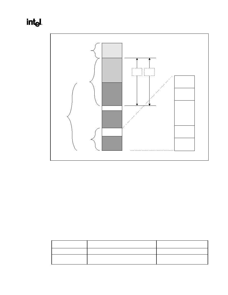
82815EP and 82815P MCH
R
Datasheet
99
mem_map
DOS Area
(640 KB)
000000h
0A0000h
09FFFFh
0C0000h
0BFFFF
h
0E0000h
0DFFFFh
0FFFFF
h
1 MB
896 KB
768 KB
640 KB
0 KB
0F0000h
0EFFFFh
960 KB
DOS
Compatibility
Memory
0 MB
Std PCI/ISA
Video Mem
(SMM Mem)
128 KB
Expansion Card
BIOS
and Buffer Area
(128 KB;
16 KB x 8)
Lower BIOS Area
(64 KB; 16 KB x 4)
Upper BIOS Area
(64 KB)
System Memory
Space
64 GB
1 MB
16 MB
640 KB
15 MB
512 MB
4 GB Max TOM
Optional ISA Hole
Main Memory
Range
PCI
Memory
Range
Extended
P6
Memory
AGP
Window
Graphics
Aperture
4.1.2. Compatibility
Area
This area is divided into the following address regions:
∑
0≠640 KB DOS Area
∑
640≠768 KB Video Buffer Area
∑
768≠896 KB in 16KB sections (total of 8 sections) ≠ Expansion Area
∑
896≠960 KB in 16KB sections (total of 4 sections) ≠ Extended System BIOS Area
∑
960 KB≠1 MB Memory (BIOS Area) ≠ System BIOS Area
The MCH supports all sixteen memory segments of interest in the compatibility area. Thirteen of the
memory ranges can be enabled or disabled independently for both read and write cycles.
Table 8. Memory Segments and Their Attributes
Memory Segments
Attributes
Comments
000000h≠09FFFFh
Fixed; always mapped to main DRAM
0 to 640K: DOS Region
0A0000h≠0BFFFFh
mapped to the hub interface or AGP ≠
configurable as SMM space
Video Buffer (physical DRAM
configurable as SMM space)
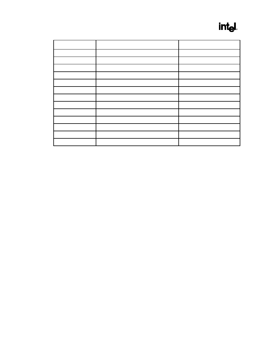
82815EP and 82815P MCH
R
100
Datasheet
Memory Segments
Attributes
Comments
0C0000h≠0C3FFFh
WE RE
Add-on BIOS
0C4000h≠0C7FFFh
WE RE
Add-on BIOS
0C8000h≠0CBFFFh
WE RE
Add-on BIOS
0CC000h≠0CFFFFh
WE RE
Add-on BIOS
0D0000h≠0D3FFFh
WE RE
Add-on BIOS
0D4000h≠0D7FFFh
WE RE
Add-on BIOS
0D8000h≠0DBFFFh
WE RE
Add-on BIOS
0DC000h≠0DFFFFh
WE RE
Add-on BIOS
0E0000h≠0E3FFFh
WE RE
BIOS Extension
0E4000h≠0E7FFFh
WE RE
BIOS Extension
0E8000h≠0EBFFFh
WE RE
BIOS Extension
0EC000h≠0EFFFFh
WE RE
BIOS Extension
0F0000h≠0FFFFFh
WE RE
BIOS Area
DOS Area (00000h≠9FFFh)
The DOS area is 640 KB and is always mapped to the main memory controlled by the MCH.

82815EP and 82815P MCH
R
Datasheet
101
Video Buffer Area (A0000h≠BFFFFh)
The 128 KB graphics adapter memory region is normally mapped to a legacy video device on the hub
interface/PCI (typically VGA controller). This area is not controlled by attribute bits and processor ≠
initiated cycles in this region are forwarded to either the hub interface or the AGP/internal graphics
device for termination. This region is also the default region for SMM space.
Accesses to this range are directed to either the hub interface or the AGP/internal graphics device based
on the configuration. The configuration is specified by:
1. AGP on/off configuration bit
2. AGP off: GMS bits of the SMRAM register in the MCH Device #0 configuration space. There is
additional steering information coming from some of the VGA registers in the Graphics device.
3. AGP on: PCICMD1 (PCI-PCI Command) and BCTRL (PCI-PCI Bridge Control) registers in
Device #1 configuration registers
The control is applied for accesses initiated from any of the system interfaces; that is, processor bus, the
hub interface, or AGP(if enabled). Note that for hub interface to AGP/PCI accesses, only memory write
operations are supported. Any AGP/PCI initiated VGA accesses targeting the MCH will master abort.
For more details, see the descriptions in the configuration registers specified above.
The SMRAM Control register controls how SMM accesses to this space are treated.
Monochrome Adapter (MDA) Range (B0000h≠B7FFFh)
Legacy support requires the ability to have a second graphics controller (monochrome) in the system.
In an AGP system, accesses in the standard VGA range are forwarded to the AGP bus (depending on
configuration bits). Since the monochrome adapter may be on the hub interface/PCI (or ISA) bus, the
MCH must decode cycles in the MDA range and forward them to the hub interface. This capability is
controlled by a configuration bit (MDA bit ≠ Device 0, BEh). In addition to the memory range B0000h
to B7FFFh, the MCH decodes IO cycles at 3B4h, 3B5h, 3B8h, 3B9h, 3Bah and 3BFh and forwards them
to the hub interface bus
Expansion Area (C0000h≠DFFFFh)
This 128 KB ISA Expansion region is divided into eight 16 KB segments. Each segment can be assigned
one of four read/write states: read only, write-only, read/write, or disabled. Typically, these blocks are
mapped through MCH and are subtractively decoded to ISA space. Memory that is disabled is not
remapped.
Extended System BIOS Area (E0000h≠EFFFFh)
This 64 KB area is divided into four 16 KB segments. Each segment can be assigned independent read
and write attributes so it can be mapped either to main DRAM or to the hub interface. Typically, this area
is used for RAM or ROM. Memory segments that are disabled are not remapped elsewhere.
System BIOS Area (F0000h≠FFFFFh)
This area is a single 64 KB segment. This segment can be assigned read and write attributes. It is by
default (after reset) read/write disabled and cycles are forwarded to the hub interface. By manipulating

82815EP and 82815P MCH
R
102
Datasheet
the read/write attributes, the MCH can "shadow" BIOS into the main DRAM. When disabled, this
segment is not remapped.
4.1.3.
Extended Memory Area
This memory area covers 100000h (1 MB) to FFFFFFFFh (4 GB-1) address range and it is divided into
the following regions:
∑
Main DRAM Memory from 1 MB to the Top of Memory; maximum of 512 MB using 128M
technology
∑
PCI Memory space from the Top of Memory to 4 GB with two specific ranges:
∑
APIC Configuration Space from FEC0_0000h (4 GB-20 MB) to FECF_FFFFh and FEE0_0000h to
FEEF_FFFFh
∑
High BIOS area from 4 GB to 4 GB≠2 MB
Main DRAM Address Range (0010_0000h to Top of Main Memory)
The address range from 1 MB to the top of main memory (TOM) is mapped to main DRAM address
range. The Top of memory is limited to 512 MB. All accesses to addresses within this range will be
forwarded to the DRAM unless a hole in this range is created.
15 MB≠16 MB Hole
A hole can be created at 15 MB≠16 MB as controlled by the fixed hole enable (FDHC register) in
Device 0 space. Accesses within this hole are forwarded to the hub interface. The range of physical
DRAM memory disabled by opening the hole is not remapped to the Top of the memory ≠ that physical
DRAM space is not accessible. This 15 MB≠16 MB hole is an optionally enabled ISA hole. Video
accelerators originally used this hole. It is also used by validation and customer SV teams for some of
their test cards. This is why it is being supported. There is no inherent BIOS request for the 15≠16 MB
hole.
Extended SMRAM Address Range (Top of Main Memory≠TSEG)
The HSEG and TSEG SMM transaction address spaces reside in this extended memory area.
HSEG
SMM-mode processor accesses to enabled HSEG are remapped to 000A0000h≠000BFFFFh. Non-SMM-
mode processor accesses to enabled HSEG are considered invalid are terminated immediately on the
FSB. The exception to this is non-SMM-mode write-back cycles. They are remapped to SMM space to
maintain cache coherency. AGP and hub interface originated cycles to enabled SMM space are not
allowed. Physical DRAM behind the HSEG transaction address is not remapped and is not accessible.
TSEG
TSEG can be up to 1 MB and is at the top of memory. SMM-mode processor accesses to enabled TSEG
access the physical DRAM at the same address. Non-SMM-mode processor accesses to enabled TSEG
are considered invalid and are terminated immediately on the FSB. The exception is non-SMM-mode
write-back cycles. They are directed to the physical SMM space to maintain cache coherency. AGP and
hub interface originated cycle to enabled SMM space are not allowed.

82815EP and 82815P MCH
R
Datasheet
103
The size of the SMRAM space is determined by the USMM value in the SMRAM register. When the
extended SMRAM space is enabled, non-SMM processor accesses and all other accesses in this range
are forwarded to the hub interface. When SMM is enabled, the amount of memory available to the
system is equal to the amount of physical DRAM minus the value in the TSEG register.
Note that there is potential for cache corruption if illegal accesses are requested to TSEG. Originally,
TSEG was intended for additional data storage for non-cached solutions. As such, it added protection as
direct reads and writes to TSEG are not allowed to occur outside of SMM. However, when the region is
enabled as cacheable, this protection can cause problems if improperly used. The reason is that, if any
piece of software (including ITP) is to read TSEG outside of SMM, the read can cause corruption of the
cached version of the code in the processor and result in a SMM "hang".
Example of Problem Manifestation:
1. SMM handler initialized and SMM code/data is written to TSEG
2. Processor cache emptied of TSEG data sometime later as cache lines are evicted and replaced
3. Rogue application requests illegal memory read to TSEG (illegal because processor is not in
SMM)
4. Processor runs memory read cycles to MCH to perform read from TSEG
5. MCH realizes processor is NOT in SMM and blocks the reads from targeting actual memory.
Instead it runs the cycle down the hub interface, which ICH2 then converts to a PCI cycle. This
typically gets master aborted and returns a floating bus (FFFFFFFFh).
6. Processor read cycles complete and FFFFFFFFh is pulled into processor cache lines.
7. Processor thinks it has valid TSEG code/data in its cache, when it really has incorrect data
(FFFFFFFFh)
8. Processor runs other system level code, evicting cache lines as needed, but some lines of
FFFFFFFFh remain
9. Eventually, an SMI is generated and this puts the processor into SMM and calls for execution of
the SMM handler stored in TSEG.
10. Processor begins fetching TSEG and hits a line in its cache read by the rogue application
(FFFFFFFFh).
11. This code is corrupted and a "hang" is eminent
The result is that the TSEG protection built into the chipset could potentially cause a system to "hang"
for cached operations, if not properly used. In fact, an application that only reads from the TSEG region
can cause SMRAM corruption by causing the SMM handler to execute bogus code fetched from the PCI
bus.
An alternative is to not use TSEG chipset features at all when running cached. Simply reserve a piece of
system memory at the top of memory region, indicate a lower actual top of memory to the operating
system (through E820h/E801h function calls), and use this region as SMRAM. As there is no restriction
that this memory cannot be accessed when not in SMM mode, then the MCH will not block accesses to
it. When it is cached, a read to the region (whether performed inside or outside of SMRAM) will return
the correct data and this coherency issue is avoided.
PCI Memory Address Range (Top of Main Memory to 4 GB)
The address range from the top of main DRAM to 4 GB (top of physical memory space supported by the
MCH) is normally mapped via the hub interface to PCI.
As an AGP configuration, there are two exceptions to this rule.

82815EP and 82815P MCH
R
104
Datasheet
∑
Addresses decoded to the AGP memory window defined by the MBASE, MLIMIT, PMBASE, and
PMLIMIT registers are mapped to AGP.
∑
Addresses decoded to the graphics aperture range defined by the APBASE and APSIZE registers
are mapped to the main DRAM.
There are two sub-ranges within the PCI memory address range defined as APIC Configuration Space
and High BIOS Address Range. As an AGP device, the AGP memory window and Graphics Aperture
Window MUST NOT overlap with these two ranges. These ranges are described in detail in the
following paragraphs.

82815EP and 82815P MCH
R
Datasheet
105
APIC Configuration Space (FEC0_0000h ≠FECF_FFFFh,
FEE0_0000h≠ FEEF_FFFFh)
This range is reserved for APIC configuration space, which includes the default I/O APIC configuration
space. The default Local APIC configuration space is FEE0_0000h to FEEF_0FFFh.
Processor accesses to the local APIC configuration space do not result in external bus activity since the
local APIC configuration space is internal to the processor. However, a MTRR must be programmed to
make the local APIC range uncacheable (UC). The local APIC base address in each processor should be
relocated to the FEC0_0000h (4 GB ≠ 20 MB) to FECF_FFFFh range so that one MTRR can be
programmed to 64 KB for the local and I/O APICs. The I/O APIC(s) usually reside in the I/O Bridge
portion (I/O Controller Hub) of the chipset or as a stand-alone component(s).
I/O APIC units will be located beginning at the default address FEC0_0000h. The first I/O APIC will be
located at FEC0_0000h. Each I/O APIC unit is located at FEC0_x000h where x is I/O APIC unit number
0 through F(hex). This address range will be normally mapped via the hub interface to PCI.
Note: There is no provision to support an I/O APIC device on AGP
The address range between the APIC configuration space and the High BIOS (FED0_0000h to
FFDF_FFFFh) is always mapped via the hub interface to PCI.
High BIOS Area (FFE0_0000h ≠FFFF_FFFFh)
The top 2 MB of the extended memory region is reserved for system BIOS (High BIOS), extended BIOS
for PCI devices, and the A20 alias of the system BIOS. The processor begins execution from the High
BIOS after reset. This region is mapped via the hub interface to PCI so that the upper subset of this
region aliases to 16 MB≠256 MB range. The actual address space required for the BIOS is less than
2 MB but the minimum processor MTRR range for this region is 2 MB so that full 2 MB must be
considered. The I/O Controller Hub supports a maximum of 1 MB in the High BIOS range.
4.1.3.1.
System Management Mode (SMM) Memory Range
The MCH supports the use of main memory as System Management RAM (SMRAM) enabling the use
of System Management Mode (SMM). The MCH supports three SMM options: Compatible SMRAM
(AB segment enabled), High Segment (HSEG), and Top of Memory Segment (TSEG). System
Management RAM (SMRAM) space provides a memory area that is available for the SMI handler's
code and data storage. This memory resource is normally hidden from the operating system so that the
processor has immediate access to this memory space upon entry to SMM. The MCH provides three
SMRAM options:
∑
Below 1 MB option that supports compatible SMI handlers.
∑
Above 1 MB option that allows new SMI handlers to execute with write-back cacheable SMRAM.
∑
Optional larger write-back cacheable T_SEG area of either 512 KB or 1MB in size above 1 MB
that is reserved from the highest area in system DRAM memory. The above 1 MB solutions
require changes to compatible SMRAM handler's code to properly execute above 1 MB.
Refer to the Power Management section for more details on SMRAM support.
Note: The hub interface and AGP masters are not allowed to access the SMM space. This must be insured even
for the GTLB translation.

82815EP and 82815P MCH
R
106
Datasheet
4.2. Memory Shadowing
Any block of memory that can be designated as read only or write-only can be "shadowed" into MCH
DRAM memory. Typically, this is done to allow ROM code to execute more rapidly out of main DRAM.
ROM is used as a read-only during the copy process while DRAM at the same time is designated write-
only. After copying, the DRAM is designated read-only so that ROM is shadowed. Processor bus
transactions are routed accordingly.
4.3. I/O Address Space
∑
The MCH never responds to I/O cycles initiated on AGP.
∑
The MCH does not support the existence of any other I/O devices other than itself on the processor
bus. The MCH generates either hub interface or AGP/PCI (if enabled) bus cycles for all processor
I/O accesses. If internal graphics is enabled, the MCH routes the access to hub interface or legacy
I/O registers supported by the internal graphics device. The MCH contains two internal registers in
the processor I/O space, Configuration Address Register (CONF_ADDR) and the Configuration
Data Register (CONF_DATA). These locations are used to implement PCI configuration space
access mechanism and as described in this document.
∑
The processor allows 64K+3 bytes to be addressed within the I/O space. The MCH propagates the
processor I/O address without any translation on to the destination bus and, therefore, provides
addressability for 64K+3 byte locations. Note that the upper 3 locations can be accessed only during
I/O address wrap-around when processor bus A16# address signal is asserted. A16# is asserted on
the processor bus when an I/O access is made to 4 bytes from address 0FFFDh, 0FFFEh, or
0FFFFh. A16# is also asserted when an I/O access is made to 2 bytes from address 0FFFFh.
∑
The I/O accesses, other than ones used for PCI configuration space access or ones that target the
internal graphics device (or AGP/PCI) are forwarded to the hub interface. The MCH will not post
I/O write cycles to IDE. The PCICMD1 or PCICMD2 register can disable the routing of I/O cycles
to the AGP.
∑
The MCH never responds to I/O cycles initiated on AGP.
4.3.1.
MCH Decode Rules and Cross-Bridge Address Mapping
The MCH's address map applies globally to accesses arriving on any of the two interfaces (i.e., Host bus
or hub interface).

82815EP and 82815P MCH
R
Datasheet
107
4.3.2.
Address Decode Rules
The MCH accepts all memory read and write accesses from the hub interface to system memory. The hub
interface accesses that fall elsewhere within the PCI memory range will not be accepted. The MCH never
responds to hub interface initiated I/O read or write cycles.
The MCH accepts accesses from the hub interface to the following address ranges:
∑
All memory read and write accesses to main DRAM including PAM region (except SMM space)
∑
All memory read/write accesses to the graphics aperture (DRAM) defined by APBASE and
APSIZE.
∑
All hub interface memory write accesses to AGP memory range defined by MBASE, MLIMIT,
PMBASE, and PMLIMIT.
∑
Memory writes to VGA range on AGP, if enabled.
The hub interface memory accesses that fall elsewhere within the memory range are considered invalid
and will be remapped to a translated memory address, snooped on the host bus, and dispatched to
DRAM. Reads will return all 1s with Master Abort completion. Writes will have byte enables deasserted
and will terminate with Master Abort, if completion is required. I/O cycles will not be accepted. They are
terminated with Master Abort completion packets.
The Hub Interface Accesses to MCH that Cross Device Boundaries
The hub interface accesses are limited to 256 bytes but have no restrictions on crossing address
boundaries. A single hub interface request may, therefore, span device boundaries (AGP, DRAM) or
cross from valid addresses to invalid addresses (or vica versa). The MCH does not support transactions
that cross device boundaries. For reads and for writes requiring completion, the MCH provides separate
completion status for each naturally-aligned 32 or 64 byte block. If the starting address of a transaction
hits a valid address, the portion of a request that hits that target device (AGP or DRAM) will complete
normally.
The remaining portion of the access that crosses a device boundary (targets a different device than that of
the starting address) or hits an invalid address will be remapped to memory address 0h, snooped on the
host bus, and dispatched to DRAM. Reads will return all 1s with Master Abort completion. Writes will
have byte enables deasserted and will terminate with Master Abort if completion is required.
If the starting address of a transaction hits an invalid address, the entire transaction will be remapped to
memory address 0h, snooped on the host bus, and dispatched to DRAM. Reads will return all 1s with
Master Abort completion. Writes will have byte enables deasserted and will terminate with Master Abort
if completion is required.

82815EP and 82815P MCH
R
108
Datasheet
4.3.2.1.
AGP Interface Decode Rules
Cycles Initiated Using PCI Protocol
The MCH does not support any AGP/PCI access targeting the hub interface. The MCH will claim
AGP/PCI initiated memory read and write transactions decoded to the main DRAM range or the graphics
Aperture range. All other memory read and write requests will be master-aborted by the AGP/PCI
initiator as a consequence of the MCH not responding to a transaction.
Under certain conditions, the MCH restricts access to the DOS compatibility ranges governed by the
PAM registers by distinguishing access type and destination bus. The MCH accepts AGP/PCI write
transactions to the compatibility ranges if the PAM designates DRAM as write-able. If accesses to a
range are not write enabled by the PAM, the MCH does not respond and the cycle results in a master-
abort. AGP/PCI read transactions to the compatibility ranges are accepted if the PAM designates DRAM
as readable. If accesses to a range are not read enabled by the PAM, the MCH does not respond and the
cycle will result in a master-abort.
If agent on AGP/PCI issues an I/O or PCI Special Cycle transaction, the MCH does not respond and
cycle results in a master-abort. The MCH does not accept PCI configuration cycles to the internal MCH
devices.
Cycles Initiated Using AGP Protocol
All cycles must reference main memory--main DRAM address range (excluding PAM) or graphics
aperture range (also physically mapped within DRAM but using different address range). AGP accesses
to the PAM region from 640 KB ≠to- 1 MB are not allowed. AGP accesses to SMM space are not
allowed. AGP-initiated cycles that target DRAM are not snooped on the host bus, even if they fall
outside of the AGP aperture range.
If a cycle is outside of a valid main memory range, then it will terminate as follows:
∑
Reads: Remap to memory address 0h, return data from address 0h, and set the IAAF error flag.
∑
Writes: Remapped to memory address 0h with byte enables deasserted (effectively dropped "on the
floor") and set the IAAF error flag.
AGP Accesses to MCH that Cross Device Boundaries
For FRAME# accesses, when an AGP or PCI master gets disconnected, it will resume at the new address
that allows the cycle to be routed to or claimed by the new target. Therefore, accesses should be
disconnected by the target on potential device boundaries. The MCH disconnects AGP/PCI transactions
on 4 KB boundaries.
AGP PIPE# and SBA accesses are limited to 256 bytes and must hit DRAM. AGP accesses are
dispatched to DRAM on naturally aligned 32-byte block boundaries. The portion of the request that hits
a valid address completes normally. The portion of a read access that hits an invalid address is remapped
to address 0h, returns data from address 0h, and sets the IAAF error flag. The portion of a write access
that hits an invalid address is remapped to memory address 0h with byte enables deasserted (effectively
dropped "on the floor") and set the IAAF error flag.

82815EP and 82815P MCH
R
Datasheet
109
4.3.2.2.
Legacy VGA Ranges
The legacy VGA memory range A0000h≠BFFFFh is mapped either to the hub interface or to AGP/PCI1
depending on the programming of the VGA Enable bit in the BCTRL configuration register in MCH
Device #1 configuration space, and the MDAP bit in the MCHCFG configuration register in Device #0
configuration space. The same register controls mapping VGA I/O address ranges. The VGA I/O range is
defined as addresses where A[9:0] are in the ranges 3B0h to 3BBh and 3C0h to 3DFh (inclusive of ISA
address aliases: A[15:10] are not decoded). The function and interaction of these two bits is described
below:
MDA Present (MDAP): This bit works with the VGA Enable bit in the BCTRL register of device 1 to
control the routing of processor-initiated transactions targeting MDA compatible I/O and memory
address ranges. This bit should not be set when the VGA Enable bit is not set. If the VGA enable bit is
set, accesses to IO address range x3BCh≠x3BFh are forwarded to the hub interface. If the VGA enable
bit is not set, I/O address range accesses x3BCh≠x3BFh are treated like other I/O accesses (the cycles are
forwarded to AGP if the address is within IOBASE and IOLIMIT and ISA enable bit is not set);
otherwise, they are forwarded to the hub interface. MDA resources are defined as the following:
Memory:
0B0000h≠0B7FFFh
I/O:
3B4h, 3B5h, 3B8h, 3B9h, 3BAh, 3BFh,
(including ISA address aliases, A[15:10] are not used in decode)
Any I/O reference that includes the I/O locations listed above, or their aliases, are forwarded to the hub
interface, even if the reference includes I/O locations not listed above.
VGA Enable: Controls the routing of processor-initiated transactions targeting VGA compatible I/O and
memory address ranges. When this bit is set, the MCH forwards the following processor accesses to
AGP:
∑
Memory accesses in the range 0A0000h to 0BFFFFh
∑
I/O addresses where A[9:0] are in the ranges 3B0h to 3BBh and 3C0h to 3DFh
(inclusive of ISA address aliases: A[15:10] are not decoded)
When this bit is set , forwarding of these accesses issued by the processor is independent of the I/O
address and memory address ranges defined by the previously defined Base and Limit registers.
Forwarding of these accesses is also independent of the settings of bit 2 (ISA Enable) of BCTRL if this
bit is 1. If the VGA enable bit is set, accesses to I/O address range x3BCh≠x3BFh are forwarded to the
hub interface. If the VGA enable bit is not set, I/O address range accesses x3BCh≠x3BFh are treated like
other I/O accesses (the cycles are forwarded to AGP, if the address is within IOBASE and IOLIMIT and
ISA enable bit is not set); otherwise, they are forwarded to the hub interface.
If this bit is 0 (default), VGA compatible memory and I/O range accesses are not forwarded to AGP;
rather, they are mapped to the hub interface, unless they are mapped to AGP via I/O and memory range
registers defined above (IOBASE, IOLIMIT, MBASE, MLIMIT, PMBASE, PMLIMIT).
The following table shows the behavior for all combinations of MDA and VGA:
VGA MDA
Behavior
0
0
All references to MDA and VGA go to the hub interface
0
1
Illegal combination (DO NOT USE)
1
0
All references to VGA Go To AGP/PCI. MDA-only references (I/O Address 3BFh and
aliases) will go to the hub interface.
1
1
VGA references go to AGP/PCI; MDA references go to the hub interface.
82815EP and 82815P MCH
R
110
Datasheet
4.4. Host Interface
The host interface of the MCH is optimized to support the Intel
Pentium
III
processor,
Intel
Pentium II processor, and Intel
Celeron
TM
processor. The MCH implements the host address,
control, and data bus interfaces within a single device. The MCH supports a 4-deep in-order queue (i.e.,
supports pipelining of up to 4 outstanding transaction requests on the host bus) . Host bus addresses are
decoded by the MCH for accesses to system memory, PCI memory and PCI I/O (via hub interface), and
PCI configuration space. The MCH takes advantage of the pipelined addressing capability of the
processor to improve the overall system performance. The MCH supports the 370-pin socket processor
connector.
4.4.1.
Host Bus Device Support
The MCH recognizes and supports a large subset of the transaction types that are defined for the Intel
Pentium
III
processor, Intel
Pentium II processor, or Intel
Celeron
TM
processor bus interface. However,
each of these transaction types have a multitude of response types, some of which are not supported by
this controller. All transactions are processed in the order that they are received on the processor bus.
Table 9. Summay of Transactions Supported By MCH
Transaction REQa[4:0]#
REQb[4:0]#
MCH
Support
Deferred Reply
0 0 0 0 0
X X X X X
The MCH will initiate a deferred reply request for a
previously deferred transaction.
Reserved
0 0 0 0 1
X X X X X
Reserved
Interrupt
Acknowledge
0 1 0 0 0
0 0 0 0 0
Interrupt acknowledge cycles are forwarded to the hub
interface.
Special
Transactions
0 1 0 0 0
0 0 0 0 1
See separate table in special cycles section.
Reserved
0 1 0 0 0
0 0 0 1 x
Reserved
Reserved
0 1 0 0 0
0 0 1 x x
Reserved
Branch Trace
Message
0 1 0 0 1
0 0 0 0 0
The MCH will terminate a branch trace message without
latching data.
Reserved
0 1 0 0 1
0 0 0 0 1
Reserved
Reserved
0 1 0 0 1
0 0 0 1 x
Reserved
Reserved
0 1 0 0 1
0 0 1 x x
Reserved
I/O Read
1 0 0 0 0
0 0 x LEN#
I/O read cycles are forwarded to hub interface. I/O cycles
that are in the MCH configuration space are not forwarded
to the hub interface.
I/O Write
1 0 0 0 1
0 0 x LEN#
I/O write cycles are forwarded to hub interface. I/O cycles
that are in the MCH configuration space are not forwarded
to the hub interface.
Reserved
1 1 0 0 x
0 0 x x x
Reserved
Memory Read &
Invalidate
0 0 0 1 0
0 0 x LEN#
Host initiated memory read cycles are forwarded to DRAM
or the hub interface.
Reserved
0 0 0 1 1
0 0 x LEN#
Reserved

82815EP and 82815P MCH
R
Datasheet
111
Transaction REQa[4:0]#
REQb[4:0]#
MCH
Support
Memory Code
Read
0 0 1 0 0
0 0 x LEN#
Memory code read cycles are forwarded to DRAM or the
hub interface.
Memory Data
Read
0 0 1 1 0
0 0 x LEN#
Host-initiated memory read cycles are forwarded to DRAM
or the hub interface.
Memory Write
(no retry)
0 0 1 0 1
0 0 x LEN#
This memory write is a writeback cycle and cannot be
retried. The MCH forwards the write to DRAM.
Memory Write
(can be retried)
0 0 1 1 1
0 0 x LEN#
The standard memory write cycle is forwarded to DRAM or
the hub interface.
NOTES:
1. For Memory cycles, REQa[4:3]# = ASZ#. MCH only supports ASZ# = 00 (32 bit address).
2. REQb[4:3]# = DSZ#. DSZ# = 00 (64 bit data bus size).
3. LEN# = data transfer length as follows:
LEN# Data
length
00
<= 8 bytes (BE[7:0]# specify granularity)
01
Length = 16 bytes BE[7:0]# all active
10
Length = 32 bytes BE[7:0]# all active
11
Reserved
Table 10. Host Responses Supported by the MCH
RS2# RS1# RS0# Description
MCH
Support
0 0 0
idle
0
0
1
Retry Response
This response is generated if an access is to a resource
that cannot be accessed by the processor at this time and
the logic must avoid deadlock . Hub interface directed
reads, writes, and DRAM locked reads can be retried.
0 1 0
Deferred
Response
This response can be returned for all transactions that can
be executed `out of order.' Hub interface directed reads
(memory, I/O and Interrupt Acknowledge) and writes (I/O
only), and internal Graphics device directed reads
(memory and I/O) and writes (I/O only) can be deferred.
0 1 1
Reserved Reserved
1
0
0
Hard Failure
Not supported.
1 0 1
No
Data
Response
This is for transactions where the data has already been
transferred or for transactions where no data is
transferred. Writes and zero length reads receive this
response.
1 1 0
Implicit
Writeback
This response is given for those transactions where the
initial transactions snoop hits on a modified cache line.
1 1 1
Normal
Data
Response
This response is for transactions where data accompanies
the response phase. Reads receive this response.

82815EP and 82815P MCH
R
112
Datasheet
4.4.2. Special
Cycles
A Special Cycle is defined when REQa[4:0] = 01000 and REQb[4:0]= xx001. The first address phase
Aa[35:3]# is undefined and can be driven to any value. The second address phase, Ab[15:8]# defines the
type of Special Cycle issued by the processor.
Table 11 specifies the cycle type and definition as well as the action taken by the MCH when the
corresponding cycles are identified.
Table 11. Special Cycles
BE[7:0]#
Special Cycle Type
Action Taken
0000 0000
NOP
This transaction has no side-effects.
0000 0001
Shutdown
This transaction is issued when an agent detects a severe software error
that prevents further processing. This cycle is claimed by the MCH. The
MCH issues a shutdown special cycle on the hub interface. This cycle is
retired on the processor bus after it is terminated on the hub interface via
a master abort mechanism.
0000 0010
Flush
This transaction is issued when an agent has invalidated its internal
caches without writing back any modified lines. The MCH claims this
cycle and retires it.
0000 0011
Halt
This transaction is issued when an agent executes a HLT instruction and
stops program execution. This cycle is claimed by the MCH and
propagated to the hub interface as a Special Halt Cycle. This cycle is
retired on the processor bus after it is terminated on the hub interface via
a master abort mechanism.
0000 0100
Sync
This transaction is issued when an agent has written back all modified
lines and has invalidated its internal caches. The MCH claims this cycle
and retires it.
0000 0101
Flush Acknowledge
This transaction is issued when an agent has completed a cache sync
and flush operation in response to an earlier FLUSH# signal assertion.
The MCH claims this cycle and retires it.
0000 0110
Stop Clock
Acknowledge
This transaction is issued when an agent enters Stop Clock mode. This
cycle is claimed by the MCH and propagated to the hub interface as a
Special Stop Grant Cycle. This cycle is completed on the processor bus
after it is terminated on the hub interface via a master abort mechanism.
0000 0111
SMI Acknowledge
This transaction is first issued when an agent enters the System
Management Mode (SMM). Ab[7]# is also set at this entry point. All
subsequent transactions from the processor with Ab[7]# set are treated
by the MCH as accesses to the SMM space. No corresponding cycle is
propagated to the hub interface. To exit the System Management Mode
the processor issues another one of these cycles with the Ab[7]# bit
deasserted. The SMM space access is closed by the MCH at this point.
All others
Reserved

82815EP and 82815P MCH
R
Datasheet
113
4.5. System Memory DRAM Interface
The MCH integrates a system DRAM controller that supports a 64-bit DRAM array. The DRAM type
supported is synchronous (SDRAM). The MCH generates the SCSA#, SCSB#, SDQM, SCAS#, SRAS#,
SWE# and multiplexed addresses, SMA for the DRAM array. The MCH's DRAM interface operates at a
clock frequency of either 100 or 133 MHz, dependent upon the system bus interface clock frequency.
The DRAM controller interface is fully configurable through a set of control registers. Complete
descriptions of these registers are given in the register description section of this document.
The MCH supports industry standard 64-bit wide DIMM modules with SDRAM devices. The 2 bank
select lines (SBS[1:0]), the 13 address lines (SMAA[12:0]), and copies of 4 address lines (SMAB[7:4]#
and SMAC[7:4]#) allow the MCH to support 64-bit wide DIMMs using 16Mbit, 64Mbit, 128Mbit, and
256Mbit technology SDRAMs. The MCH has a sufficient amount of SCS# lines to enable the support of
up to six 64-bit rows of DRAM. For write operations of less than a QWord, the MCH performs a byte-
wise write. The MCH targets SDRAM with CL2 and CL3 and supports both single and double-sided
DIMMs. The MCH provides refresh functionality with programmable rate (normal DRAM rate is
1 refresh/15.6
µ
s). The MCH can be configured via the Page Closing Policy Bit in the MCH
Configuration Register to keep multiple pages open within the memory array. Pages can be kept open in
any one row of memory. Up to 4 pages can be kept open within that row (The MCH only supports 4
Bank SDRAMs on system DRAM interface).
4.5.1.
DRAM Organization and Configuration
The MCH supports 64-bit DRAM configurations. In the following discussion the term row refers to a set
of memory devices that are simultaneously selected by a SCS# signal. The MCH supports a maximum of
6 rows of memory. Both single-sided and double-sided DIMMs are supported.
The interface consists of the following pins:
Multiple copies: SMAA[7:4], SMAB[7:4]# , SMAC[7:4]#
Single Copies: SMD[63:0]
SDQM[7:0]
SMAA[12:8,3:0]
SBS[1:0]
SCSA[5:0]#
SCSB[5:0]#
SCAS#
SRAS#
SWE#
SCKE[1:0]
The MCH supports DIMMs populated with 8, 16, and 32 bit wide SDRAM devices. Registered DIMMs
or DIMMs populated with 4 bit wide SDRAM devices are not supported. The MCH supports 3.3V
standard SDRAMs.

82815EP and 82815P MCH
R
114
Datasheet
Table 12 illustrates a sample of the possible DIMM socket configurations along with corresponding DRP
programming. See the register section of this document for a complete DRP programming table.
Table 12. Sample Of Possible Mix And Match Options For 4 Row/2 DIMM Configurations
DIMM0 DIMM1
DRP
Total
Memory
0
4x(4M x 16 ) S
70
32 MB
4x (4M x16 ) S
0
07
32 MB
4x(4Mx16) + 2x(2Mx32) D
0
08
48 MB
4x(4Mx16) S
4x(4Mx16) S
77
64 MB
8x(8Mx8) + 4x(4Mx16) D
0
0B
96 MB
8x(8Mx8) D
0
0C
128 MB
8x(8Mx8) D
8x(8Mx8) D
CC
256 MB
NOTES:
1. "S" denotes single-sided DIMMs, "D" denotes double-sided DIMMs.
4.5.1.1.
Configuration Mechanism For DIMMs
Detection of the type of DRAM installed on the DIMM is supported via Serial Presence Detect
mechanism as defined in the JEDEC 168-pin DIMM standard. This standard uses the SCL, SDA and
SA[2:0] pins on the DIMMs to detect the type and size of the installed DIMMs. No special
programmable modes are provided on the MCH for detecting the size and type of memory installed.
Type and size detection must be done via the serial presence detection pins. Use of Serial Presence
Detection is required.
Memory Detection and Initialization
Before any cycles to the memory interface can be supported, the MCH DRAM registers must be
initialized. The MCH must be configured for operation with the installed memory types. Detection of
memory type and size is done via the System Management Bus (SMBus) interface on the I/O Controller
Hub. This two wire bus is used to extract the DRAM type and size information from the serial presence
detect port on the DRAM DIMM modules.
DRAM DIMM modules contain a 5-pin serial presence detect interface, including SCL (serial clock),
SDA (serial data) and SA[2:0]. Devices on the SMBus bus have a seven bit address. For the DRAM
DIMM modules, the upper four bits are fixed at 1010. The lower three bits are strapped on the SA[2:0]
pins. SCL and SDA are connected directly to the System Management Bus on the I/O Controller Hub.
Thus, data is read from the Serial Presence Detect port on the DRAM DIMM modules via a series of IO
cycles to the I/O Controller Hub. BIOS essentially needs to determine the size and type of memory used
for each of the four rows of memory in order to properly configure the MCH system memory interface.
SMBus Configuration and Access of the Serial Presence Detect Ports
For more details on this, see the Intel
Æ
82801BA (ICH2) I/O Controller Hub datasheet.

82815EP and 82815P MCH
R
Datasheet
115
4.5.1.2.
DRAM Register Programming
This section provides an overview of how the required information for programming the DRAM registers
is obtained from the Serial Presence Detect ports on the DIMMs. The Serial Presence Detect ports are
used to determine Refresh Rate, MA and MD Buffer Strength, Row Type (on a row by row basis),
SDRAM Timings, Row Sizes and Row Page Sizes. Table 13 lists a subset of the data available through
the on-board Serial Presence Detect ROM on each DIMM module.
Table 13. Data Bytes on DIMM Used for Programming DRAM Registers
Byte Function
2
Memory Type (EDO, SDRAM) the MCH only supports SDRAM.
3
# of Row Addresses, not counting Bank Addresses
4
# of Column Addresses
5
# of banks of DRAM (Single or Double sided) DIMM
12
Refresh Rate
17
# Banks on each SDRAM Device
36≠41
Access Time from Clock for CAS# Latency 1 through 7
42
Data Width of SDRAM Components
Table 13 is only a subset of the defined SPD bytes on the DIMM module. These bytes collectively
provide enough data for BIOS to program the MCH DRAM registers.
4.5.2.
DRAM Address Translation and Decoding
The MCH translates the address received on the host bus, hub interface, or from the internal graphics
device to an effective memory address. The MCH supports 16Mbit, 64Mbit, 128Mbit, and 256Mbit
SDRAM devices. The MCH supports a 2 KB page sizes only. The multiplexed row / column address to
the DRAM memory array is provided by the SBS[1:0] and SMAA[11:0] signals and copies. These
addresses are derived from the host address bus as defined by by the following table for SDRAM
devices.
∑
Row size is internally computed using the values programmed in the DRP register.
∑
Up to 4 pages can be open at any time within any row (Only 2 active pages are supported in rows
populated with either 8 MBs or 16 MBs ).
82815EP and 82815P MCH
R
116
Datasheet
Table 14. MCH DRAM Address Mux Function
Address Usage
BS
BS
MA
MA
MA
MA
MA
MA
MA
MA
MA
MA
MA
MA
MA
Tech
(Mb)
De
p
t
h
W
i
dth
Row Col Bank
Mem
Size
(MB)
1 0 12 11
10 9 8 7 6 5 4 3 2 1 0
16 2M 8 11 9 1
16 X 11 X X [A] 22 21 20 19 18 17 16 15 14 13
X 11 X X PA X 23
10 9 8 7 6 5 4 3
64 8M 8 12 9 2
64 12 11 X 24 [A] 22 21 20 19 18 17 16 15 14 13
12
11 X X PA X 25
10 9 8 7 6 5 4 3
64 4M 16 12 8 2
32 12 11 X 24 [A] 22 21 20 19 18 17 16 15 14 13
12
11 X X PA X X 10 9 8 7 6 5 4 3
128 16M 8 12 10 2 128 12 11 X 24 [A] 22 21 20 19 18 17 16 15 14 13
12
11 X X PA
26 25
10 9 8 7 6 5 4 3
128 8M 16 12 9 2
64 12 11 X 24 [A] 22 21 20 19 18 17 16 15 14 13
12
11 X X PA X 25
10 9 8 7 6 5 4 3
256 32M 8 13 10 2 256 12 11 27 24 [A] 22 21 20 19 18 17 16 15 14 13
12
11 X X PA
26 25
10 9 8 7 6 5 4 3
256 16M 16 13 9 2 128 12 11 26 24 [A] 22 21 20 19 18 17 16 15 14 13
12
11 X X PA X 25
10 9 8 7 6 5 4 3
NOTES:
MA bit 10 at RAS time uses the XOR of Address bit 12 and Address bit 23
4.5.3.
DRAM Array Connectivity
Figure 6. DRAM Array Sockets
SCS[3:2]#
SCS[1:0]#
SCKE0
SCKE1
SRAS#
SCAS#
SWE#
SBS[1:0]
SMAA[12:8,3:0]
SMAA[7:4]
SMAB[7:4]#
SDQM[7:0]
SMD[63:0]
DIMM_CLK[3:0]
DIMM_CLK[7:4]
SMB_CLK
SMB_DATA
Note:
Min (16Mbit) 8MB
Max (64Mbit) 256MB
Max (128Mbit) 512MB
mem_dimm

82815EP and 82815P MCH
R
Datasheet
117
4.5.4.
SDRAMT Register Programming
Several DRAM timing parameters are programmable in the MCH configuration registers. Table 15
summarizes the programmable parameters.
Table 15. Programmable SDRAM Timing Parameters
Parameter
DRAMT Bit
Values (SCLKs)
RAS# Precharge (SRP)
0
2,3
RAS# to CAS# Delay (SRCD)
1
2,3
CAS# Latency (CL)
2
2,3
DRAM Cycle Time (DCT)
4
Tras = 5,6
Trc = 7,8
These parameters are controlled via the DRAMT register. To support different device speed grades,
CAS# Latency, RAS# to CAS# Delay, and RAS# Precharge are all programmable as either two or three
SCLKs. To provide flexibility, these are each controlled by separate register bits (i.e., the MCH can
support any combination of CAS# Latency, RAS#-to-CAS# Delay and RAS# Precharge).
4.5.5.
SDRAM Paging Policy
The MCH can maintain up to 4 active pages in any one row; however, the MCH does not support active
pages in more than 1 row at a time.
The DRAM page closing policy (DPCP) in the MCH configuration register (MCHCFG) controls the
page closing policy of the MCH. This bit controls whether the MCH "precharges bank" or "precharges
all" during the service of a page miss. When this bit is 0, the MCH prechanges bank during the service of
a page miss. When this bit is 1, the MCH prechanges all during the service of a page miss.
4.6. System Reset for the MCH
Refer to the Intel
815EP Chipset Design Guide or Intel
815EP Chipset Design Guide (Power
Sequencing section) for details.
4.7. System Clock Description
The Intel
815EP chipset family is supported by the CK815 chipset 2DIMM and CK815 chipset 3DIMM
clock synthesizers. For details, refer to the Intel
815EP Chipset Design Guide or Intel
815EP Chipset
Design Guide.

82815EP and 82815P MCH
R
118
Datasheet
4.8. Power Management
4.8.1. Specifications
Supported
The platform is compliant with the following specifications:
∑
APM Rev 1.2
∑
ACPI Rev 1.0
∑
PCI Power Management Rev 1.0
∑
PC 99 System Design Guide, Rev 1.0

82815EP and 82815P MCH
R
Datasheet
119
5.
Pinout and Package Information
5.1. 82815EP MCH Pinout
Figure 10 and Figure 11 show the ball foot print of the MCH. These figures represent the ballout by ball
number. Table 16 provides an alphabetical signal listing of the ballout.
The following Notes apply to Figure 10, Figure 11, and Table 22:
NOTES:
NC = No Connect. These pins should float
PU = Pull Up. These GPIO(x) related pins should be pulled up to the appropriate voltage
through a weak pull-up resistor (8.2K to 10K Ohm resistor.) The appropriate voltage
depends upon in which voltage well the GPIO(x) resides. Typically, this is the 3.3V core
voltage well.
PD = Pull Down. These pins should be pulled down to ground through a weak pull-down
resistor. (8.2K to 10K Ohm resistor.)
VSS = Connect to ground.
PU1.8 = Pull Up to 1.8V through a weak pull-up resistor. (8.2K to 10K Ohm resistor.)

82815EP and 82815P MCH
R
120
Datasheet
Figure 7. MCH Pinout (Top View-Left Side)
1 2 3 4 5 6 7 8 9 10 11 12 13
A
SMD17 SMD49 SMD16 SMD48 SDQM7 SDQM3 SDQM2 SCSB5# SMAC7# SMAC5# SMAA7 SMAA5 SMAA11
B
SMD50 VSUS3.3 SMD56 SMD23 VSUS3.3 SDQM6 SMAA12 VSUS3.3 SCSB4# SMAC4# VSUS3.3 SMAA4 SBS0
C
SMD18
SMD25 VSS SMD55
SMD22 VSS SCKE5
SCKE4 VSS SMAC6#
SMAA6 VSS SMAA9
D
VSS SMD57 SMD26 SMD24 SMD54 SMD21 SCKE3 SCKE0 SCSB3# SCSB2# SBS1 SMAA8 SMAA0
E
SMD51
VSUS3.3
SMD58
SMD27 VSS SMD53 VSS SCKE1
SCKE2 VSS SMAA10 VSS SCSA4#
F
VSS SMD19 VSS SMD59
SMD28
SMD60 SCLK
SCSB1#
SCSB0#
VSUS3.3 VSS SMAA2 VSS
G
ADS# SMD52 SMD20 SMD29 SMD61 VSUS3.3
SRCOMP
VSUS3.3 VSS
NC
H
RS2#
VSUS3.3
RESET#
SMD62
VSUS3.3
VSS
VSUS3.3
J
DRDY#
VSS
DBSY#
SMD63
VSS
SMD30
VCCDPLL
K
HIT#
RS0#
HTRDY#
VSS
SMD31
V1.8
VSSDPLL
L
RS1#
VSS
HITM#
HLOCK#
HREQ3#
VSS
VSS
VSS
VSS
M
HREQ0#
HREQ2#
DEFER#
VSS
BPRI#
V1.8
VSS
VSS
VSS
N
HREQ1#
VSS
HREQ4#
BNR#
HA7#
VSS
VSS
VSS
VSS
P
HA4#
HA11#
HA14#
VSS
HA8#
V1.8
VSS
VSS
VSS
R
HA9#
VSS
HA6#
HA3#
HA16#
VSS
VSS
VSS
VSS
T
HA12# HA5# HA13# VSS HA15# V1.8
VSS VSS VSS
U
HA10#
VSS
HA28#
HA21#
HA25#
GTLREF0
VSS
V
HA31#
HA22#
HA19#
VSS
HA17#
VSS
V1.8
W
HA20#
VSS
HA23#
HA24#
HA30#
V1.8
VSS
Y
HA29# HA18# HA27# VSS HA26# VSS V1.8 VSS V1.8 VSS
AA
HD0# VSS HD6# HD15#
CPURST#
V1.8 HCLK V1.8 VSS
GTLREF1
V1.8 VSS V1.8
AB
HD4# HD1# HD5# VSS HD23# HD19# HD31# HD34# HD37# HD42# HD41# HD48# HD55#
AC
HD8# VSS HD17# HD7# VSS HD25# VSS HD22# VSS HD44# VSS HD63# VSS
AD
HD10# HD12# HD13# HD3# HD30# HD16# HD33# HD29# HD43# HD39# HD27# HD47# HD59#
AE
HD18# VSS HD11# VSS HD21# VSS HD35# VSS HD36# VSS HD49# VSS HD57#
AF
HD14# HD2# HD9# HD20# HD24# HD26# HD32# HD28# HD38# HD45# HD51# HD40# HD52#
1 2 3 4 5 6 7 8 9 10 11 12 13

82815EP and 82815P MCH
R
Datasheet
121
Figure 8. MCH Pinout (Top View-Right Side)
14
15 16 17 18 19 20 21 22 23 24 25 26
SMAB7#
SMAB5#
SMAA3 SCSA1# SDQM4 SMD47
SMD45 SMD42 SMD39 SMD37 SMD35 SMD33 SMD32
A
VSUS3.3 SMAB4# SMAA1
SCSA5#
SMD12
VSUS3.3
SMD44
SMD41
VSUS3.3
SMD36
SMD34
VSUS3.3
VSS
B
SMAB6#
VSS
SRAS#
SDQM5
VSS SMD46 SMD43 VSS
SMD38
SMD1 VSS V1.8 HL10
C
SCSA2#
SCSA0#
SDQM0
SMD15
SCAS#
SMD10 SMD7
SMD40
SMD2
SMD0 HL9 HL8 HL7
D
SCSA3# VSS SWE#
VSS
SMD11
SMD9
VSS
SMD4 VSSBA VCCBA
V1.8
HL6
HL5
E
VSUS3.3
SDQM1
VSS
VSUS3.3
SMD13 SMD8 SMD6 SMD3
HLCLK
V1.8 HL4 VSS
HLPSTRB#
F
VSS
SMD14
VSUS3.3
SMD5
VSS
V1.8
VSS
HL3
HLPSTRB
V1.8
G
HLZCOMP
HLREF
VSS
G_C/BE0#
HL0
HL2
HL1
H
G_AD5
G_AD3
G_AD1
VSS
AGPREF
VSS
GRCOMP
J
VDDQ
VSS
G_AD8
G_AD7
VSS
G_AD2
G_AD0
K
VSS VSS VSS
VDDQ VSS AD_STB0#
G_AD4 VSS G_AD6
L
VSS VSS VSS
G_AD12
AD_STB0 VDDQ G_AD10 G_AD9 G_AD11
M
VSS VSS VSS
G_C/BE1#
G_AD14 VSS G_AD13 VDDQ G_AD15
N
VSS VSS VSS
G_TRDY# PD G_IRDY# VSS G_STOP#
G_DEVSEL#
P
VSS VSS VSS
VDDQ NC
VSS G_PAR VSS
G_FRAME#
R
VSS
VSS
VSS
VSS
G_AD17 G_AD19 G_AD21 G_C/BE2# G_AD16
T
VDDQ
G_AD23
AD_STB1
VDDQ
G_AD18
VDDQ
G_AD20
U
VSS
G_AD25
VSS
AD_STB1#
G_AD22
G_AD24
G_AD26
V
VDDQ G_AD27
G_AD29 VSS G_AD28 VSS G_AD30
W
VSS
V1.8 VSS PD
G_AD31
SBA6
SB_STB
VDDQ
SBA7
G_C/BE3#
Y
VSS V1.8 VSS V1.8
PU
V1.8
PU
VCCDA SBA4 VSS SB_STB# VSS SBA5
AA
HD53# HD56# V1.8
NC
PU
NC
V1.8
PU
SBA0
SBA2
WBF#
SBA1
SBA3
AB
HD58# VSS
NC
VSS
PU1.8
VSS
NC
VSS
V1.8
ST2
ST1
VSS
PIPE#
AC
HD46#
HD60#
NC NC NC V1.8 NC NC NC PD ST0
G_GNT#
RBF#
AD
VSS
HD50#
VSS NC VSS NC
VSS NC NC NC PD VSS
G_REQ#
AE
HD54#
HD62#
HD61#
NC NC NC
NC NC NC NC VSS
VCCDACA2
VCCDACA1
AF
14
15 16 17 18 19 20 21 22 23 24 25 26

82815EP and 82815P MCH
R
122
Datasheet
Table 16. Alphabetical Pin Assignment
Signal Name
Ball #
ADS# G1
AD_STB0 M22
AD_STB0# L23
AD_STB1 U22
AD_STB1# V23
AGPREF J24
NC AE23
BNR# N4
BPRI# M5
CPURST# AA5
DBSY# J3
PD AE24
PU AB18
PU AA18
DEFER# M3
DRDY# J1
G_AD0 K26
G_AD1 J22
G_AD2 K25
G_AD4 L24
G_AD5 J20
G_AD6 L26
G_AD7 K23
G_AD8 K22
G_AD9 M25
G_AD10 M24
G_AD11 M26
G_AD12 M21
G_AD13 N24
G_AD14 N22
G_AD15 N26
G_AD16 T26
G_AD17 T22
G_AD18 U24
G_AD19 T23
Signal Name
Ball #
G_AD20 U26
G_AD21 T24
G_AD22 V24
G_AD23 U21
G_AD24 V25
G_AD25 V21
G_AD26 V26
G_AD27 W21
G_AD28 W24
G_AD29 W22
G_AD3 J21
G_AD30 W26
G_AD31 Y21
G_C/BE0# H23
G_C/BE1# N21
G_C/BE2# T25
G_C/BE3# Y26
G_DEVSEL# P26
G_FRAME# R26
G_GNT# AD25
G_IRDY# P23
G_PAR R24
GRCOMP J26
NC AE22
G_REQ# AE26
G_STOP# P25
GTLREF0 U6
GTLREF1 AA10
G_TRDY# P21
HA3# R4
HA4# P1
HA5# T2
HA6# R3
HA7# N5
HA8# P5
HA9# R1
Signal Name
Ball #
HA10# U1
HA11# P2
HA12# T1
HA13# T3
HA14# P3
HA15# T5
HA16# R5
HA17# V5
HA18# Y2
HA19# V3
HA20# W1
HA21# U4
HA22# V2
HA23# W3
HA24# W4
HA25# U5
HA26# Y5
HA27# Y3
HA28# U3
HA29# Y1
HA30# W5
HA31# V1
HCLK AA7
HD0# AA1
HD1# AB2
HD2# AF2
HD3# AD4
HD4# AB1
HD5# AB3
HD6# AA3
HD7# AC4
HD8# AC1
HD9# AF3
HD10# AD1
HD11# AE3
HD12# AD2
Signal Name
Ball #
HD13# AD3
HD14# AF1
HD15# AA4
HD16# AD6
HD17# AC3
HD18# AE1
HD19# AB6
HD20# AF4
HD21# AE5
HD22# AC8
HD23# AB5
HD24# AF5
HD25# AC6
HD26# AF6
HD27# AD11
HD28# AF8
HD29# AD8
HD30# AD5
HD31# AB7
HD32# AF7
HD33# AD7
HD34# AB8
HD35# AE7
HD36# AE9
HD37# AB9
HD38# AF9
HD39# AD10
HD40# AF12
HD41# AB11
HD42# AB10
HD43# AD9
HD44# AC10
HD45# AF10
HD46# AD14
HD47# AD12
HD48# AB12

82815EP and 82815P MCH
R
Datasheet
123
Signal Name
Ball #
HD49# AE11
HD50# AE15
HD51# AF11
HD52# AF13
HD53# AB14
HD54# AF14
HD55# AB13
HD56# AB15
HD57# AE13
HD58# AC14
HD59# AD13
HD60# AD15
HD61# AF16
HD62# AF15
HD63# AC12
HIT# K1
HITM# L3
HL0 H24
HL1 H26
HL2 H25
HL3 G24
HL4 F24
HL5 E26
HL6 E25
HL7 D26
HL8 D25
HL9 D24
HL10 C26
HLCLK F22
HLOCK# L4
HLPSTRB G25
HLPSTRB# F26
HLREF H21
HLZCOMP H20
HREQ0# M1
HREQ1# N1
HREQ2# M2
Signal Name
Ball #
HREQ3# L5
HREQ4# N3
NC AF23
HTRDY# K3
PD AD23
PD Y20
NC R22
PD P22
NC AB19
PU AB21
PU1.8 AC18
NC
AE19
NC
AF19
PU AA20
NC AD16
NC AF17
NC AE21
NC AD21
NC AE17
NC AD17
NC AF18
NC AD18
NC AF20
NC AD20
NC AC20
NC AF21
NC AB17
NC AC16
NC G10
PIPE# AC26
RBF# AD26
NC AD22
RESET# H3
RS0# K2
RS1# L1
RS2# H1
SBA0 AB22
Signal Name
Ball #
SBA1 AB25
SBA2 AB23
SBA3 AB26
SBA4 AA22
SBA5 AA26
SBA6 Y22
SBA7 Y25
SBS0 B13
SBS1 D11
SB_STB Y23
SB_STB# AA24
SCAS# D18
SCKE0 D8
SCKE1 E8
SCKE2 E9
SCKE3 D7
SCKE4 C8
SCKE5 C7
SCLK F7
SCSA0# D15
SCSA1# A17
SCSA2# D14
SCSA3# E14
SCSA4# E13
SCSA5# B17
SCSB0# F9
SCSB1# F8
SCSB2# D10
SCSB3# D9
SCSB4# B9
SCSB5# A8
SDQM0 D16
SDQM1 F15
SDQM2 A7
SDQM3 A6
SDQM4 A18
SDQM5 C17
Signal Name
Ball #
SDQM6 B6
SDQM7 A5
SMAA0 D13
SMAA1 B16
SMAA10 E11
SMAA11 A13
SMAA12 B7
SMAA2 F12
SMAA3 A16
SMAA4 B12
SMAA5 A12
SMAA6 C11
SMAA7 A11
SMAA8 D12
SMAA9 C13
SMAB4# B15
SMAB5# A15
SMAB6# C14
SMAB7# A14
SMAC4# B10
SMAC5# A10
SMAC6# C10
SMAC7# A9
SMD0 D23
SMD1 C23
SMD2 D22
SMD3 F21
SMD4 E21
SMD5 G20
SMD6 F20
SMD7 D20
SMD8 F19
SMD9 E19
SMD10 D19
SMD11 E18
SMD12 B18
SMD13 F18

82815EP and 82815P MCH
R
124
Datasheet
Signal Name
Ball #
SMD14 G18
SMD15 D17
SMD16 A3
SMD17 A1
SMD18 C1
SMD19 F2
SMD20 G3
SMD21 D6
SMD22 C5
SMD23 B4
SMD24 D4
SMD25 C2
SMD26 D3
SMD27 E4
SMD28 F5
SMD29 G4
SMD30 J6
SMD31 K5
SMD32 A26
SMD33 A25
SMD34 B24
SMD35 A24
SMD36 B23
SMD37 A23
SMD38 C22
SMD39 A22
SMD40 D21
SMD41 B21
SMD42 A21
SMD43 C20
SMD44 B20
SMD45 A20
SMD46 C19
SMD47 A19
SMD48 A4
SMD49 A2
SMD50 B1
Signal Name
Ball #
SMD51 E1
SMD52 G2
SMD53 E6
SMD54 D5
SMD55 C4
SMD56 B3
SMD57 D2
SMD58 E3
SMD59 F4
SMD60 F6
SMD61 G5
SMD62 H4
SMD63 J4
SRAS# C16
SRCOMP G7
ST0 AD24
ST1 AC24
ST2 AC23
SWE# E16
V1.8 C25
V1.8 T6
V1.8 V7
V1.8 W6
V1.8 AA6
V1.8 Y9
V1.8 Y18
V1.8 AA8
V1.8 AA11
V1.8 AA13
V1.8 AA15
V1.8 E24
V1.8 AA17
V1.8 AA19
V1.8 AD19
V1.8 AC22
V1.8 AB16
V1.8 AB20
Signal Name
Ball #
V1.8 F23
V1.8 G22
V1.8 G26
V1.8 K6
V1.8 M6
V1.8 P6
V1.8 Y7
VCCBA E23
VCCDA AA21
VCCDACA1 AF26
VCCDACA2 AF25
VCCDPLL J7
VDDQ N25
VDDQ K20
VDDQ L21
VDDQ M23
VDDQ U25
VDDQ R21
VDDQ U23
VDDQ W20
VDDQ Y24
VDDQ U20
VSS F1
VSS AA12
VSS AC11
VSS P14
VSS P15
VSS P16
VSS P4
VSS R11
VSS R12
VSS R13
VSS R14
VSS R15
VSS R16
VSS AC13
VSS R2
Signal Name
Ball #
VSS R23
VSS R25
VSS R6
VSS T11
VSS T12
VSS T13
VSS T14
VSS T15
VSS T16
VSS AC15
VSS T21
VSS T4
VSS U2
VSS K24
VSS U7
VSS V22
VSS V4
VSS V6
VSS W2
VSS AC17
VSS V20
VSS W23
VSS W25
VSS W7
VSS Y10
VSS Y17
VSS P13
VSS Y4
VSS Y8
VSS AC19
VSS AC2
VSS AC21
VSS AC25
VSS AC5
VSS AC7
VSS AA14
VSS AC9

82815EP and 82815P MCH
R
Datasheet
125
Signal Name
Ball #
VSS AE10
VSS AE12
VSS AE14
VSS AE16
VSS AE18
VSS AE2
VSS AE20
VSS AE4
VSS AE6
VSS AA16
VSS AE8
VSS B26
VSS C12
VSS C15
VSS C18
VSS C21
VSS C24
VSS C3
VSS C6
VSS C9
VSS AA2
VSS D1
VSS E10
VSS E12
VSS E15
VSS E17
VSS E20
Signal Name
Ball #
VSS E5
VSS E7
VSS F11
VSS AA25
VSS F13
VSS F16
VSS F25
VSS F3
VSS G17
VSS G21
VSS G23
VSS G9
VSS Y6
VSS H22
VSS H6
VSS J2
VSS J23
VSS J25
VSS J5
VSS K4
VSS L11
VSS AA9
VSS L12
VSS L13
VSS L14
VSS L15
VSS L16
Signal Name
Ball #
VSS L2
VSS L22
VSS L25
VSS L6
VSS M11
VSS AA23
VSS M12
VSS M13
VSS M14
VSS M15
VSS M16
VSS K21
VSS M4
VSS N11
VSS N12
VSS N13
VSS AB4
VSS N14
VSS N15
VSS N16
VSS N2
VSS N23
VSS P24
VSS N6
VSS P11
VSS P12
VSSBA E22
Signal Name
Ball #
VSS Y19
VSS AE25
VSS AF24
VSSDPLL K7
VSUS3.3 F14
VSUS3.3 B2
VSUS3.3 F10
VSUS3.3 F17
VSUS3.3 G6
VSUS3.3 G8
VSUS3.3 H2
VSUS3.3 H5
VSUS3.3 H7
VSUS3.3 G19
VSUS3.3 B5
VSUS3.3 B8
VSUS3.3 B11
VSUS3.3 B14
VSUS3.3 B19
VSUS3.3 B22
VSUS3.3 B25
VSUS3.3 E2
NC AF22
WBF# AB24
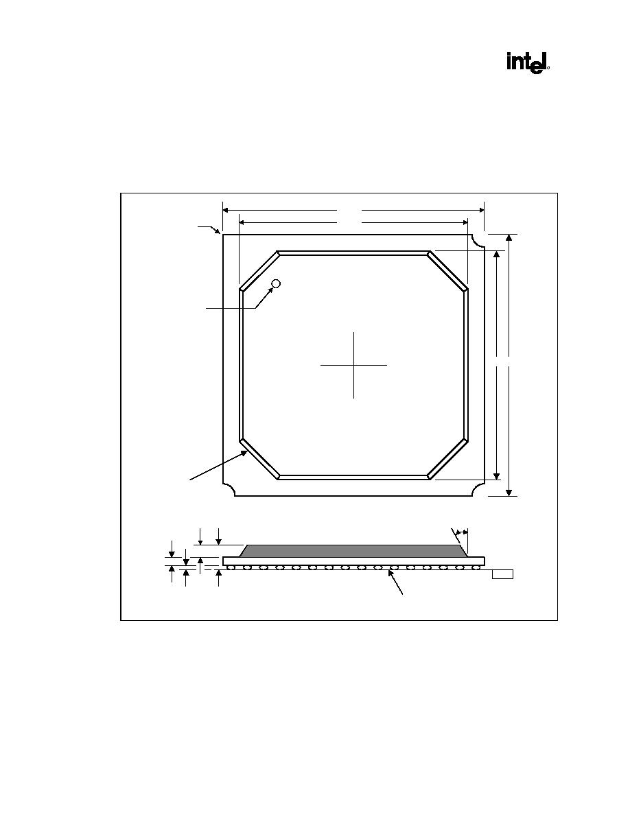
82815EP and 82815P MCH
R
126
Datasheet
5.2. Package Information
This specification outlines the mechanical dimensions for the MCH. The package is a 544 ball grid array
(BGA).
Figure 9. MCH BGA Package Dimensions (Top and Side Views)
Pin A1 I.D.
Pin A1 corner
D
D1
E
E1
Top View
A
A2
A1
c
Side View
pkgbga_top&side.vsd
Seating Plane
-C-
45∞ Chamfer
(4 places)
30∞

82815EP and 82815P MCH
R
Datasheet
127
Figure 10. MCH BGA Package Dimensions (Bottom View)
pkgbga_544.vsd
Pin A1 corner
e
544 BGA
Bottom View
2
10
16
20
22
3
5
7
9
11
13
15
17
19
1
21
23
4
6
18
8
12
14
A
B
C
D
E
F
G
H
J
K
L
P
R
T
U
V
Y
AB
AA
AC
N
W
M
j
l
e
b
24
25
26
AD
AE
AF
Table 17. Package Dimensions
Symbol Min
Nominal
Max
Units Note
A 2.17
2.38
2.59 mm
A1 0.50
0.60
0.70
mm
A2 1.12
1.17
1.22
mm
D 34.80
35.00
35.20 mm
D1 29.75
30.00
30.25
mm
E 34.80
35.00
35.20 mm
E1 29.75
30.00
30.25
mm
e
1.27 (solder ball pitch)
mm
I 1.63
REF. mm
J 1.63
REF. mm
M
26 x 26 Matrix
mm
b
2
0.60
0.75
0.90 mm
c 0.55
0.61
0.67 mm
NOTES:
1. All dimensions and tolerances conform to ANSI Y14.5-1982
2. Dimension is measured at maximum solder ball diameter parallel to primary datum (-C-)
3. Primary Datum (-C-) and seating plane are defined by the spherical crowns of the solder balls.

82815EP and 82815P MCH
R
128
Datasheet
This page is intentionally left blank.
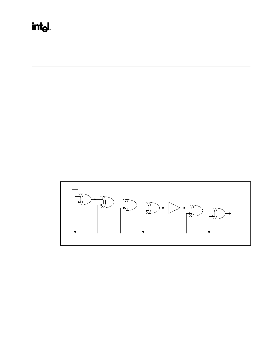
82815EP and 82815P MCH
R
Datasheet
129
6. Testability
In the 82815EP MCH, the testability for Automated Test Equipment (ATE) board level testing has been
changed from the traditional NAND chain mode to a XOR chain. The MCH pins are grouped in eight
XOR chains.
Because the 82815EP MCH device has defined pins previously found in 82815E XOR chains as Pull-
Ups and Pull-Downs, board level XOR testing can no longer be completely tested as was done with the
82815E device. The affected XOR chains are #3 and #6. These two chains have pins in them that should
either pulled up or pulled down externally on an 815EP board. The initialization of chains #7 and #8 are
also affected by the renaming of the 815E LTVCK pin to "PU" (pull-up) on the 815EP device. The
impact of these changes is:
- On platforms designed specifically for 82815EP devices, XOR chains #3, #6, #7, and #8
cannot be tested.
An XOR-Tree is a chain of XOR gates each with one of its inputs connected to a MCH input pin or bi-
directional pin (used as an input pin only). The other input of each XOR gate connects to the non-
inverted output of the previous XOR gate in the chain. The first XOR gate of each chain will have one
pin internally connected tied to Vcc. The output of the last XOR gate is the chain output. Figure 11
shows the MCH XOR chain implementation.
Figure 11. XOR Tree Implementation
Vcc
Pin 1
XOR
Out
xor.vsd
Pin 2
Pin 3
Pin 4
Pin 5
Pin 6
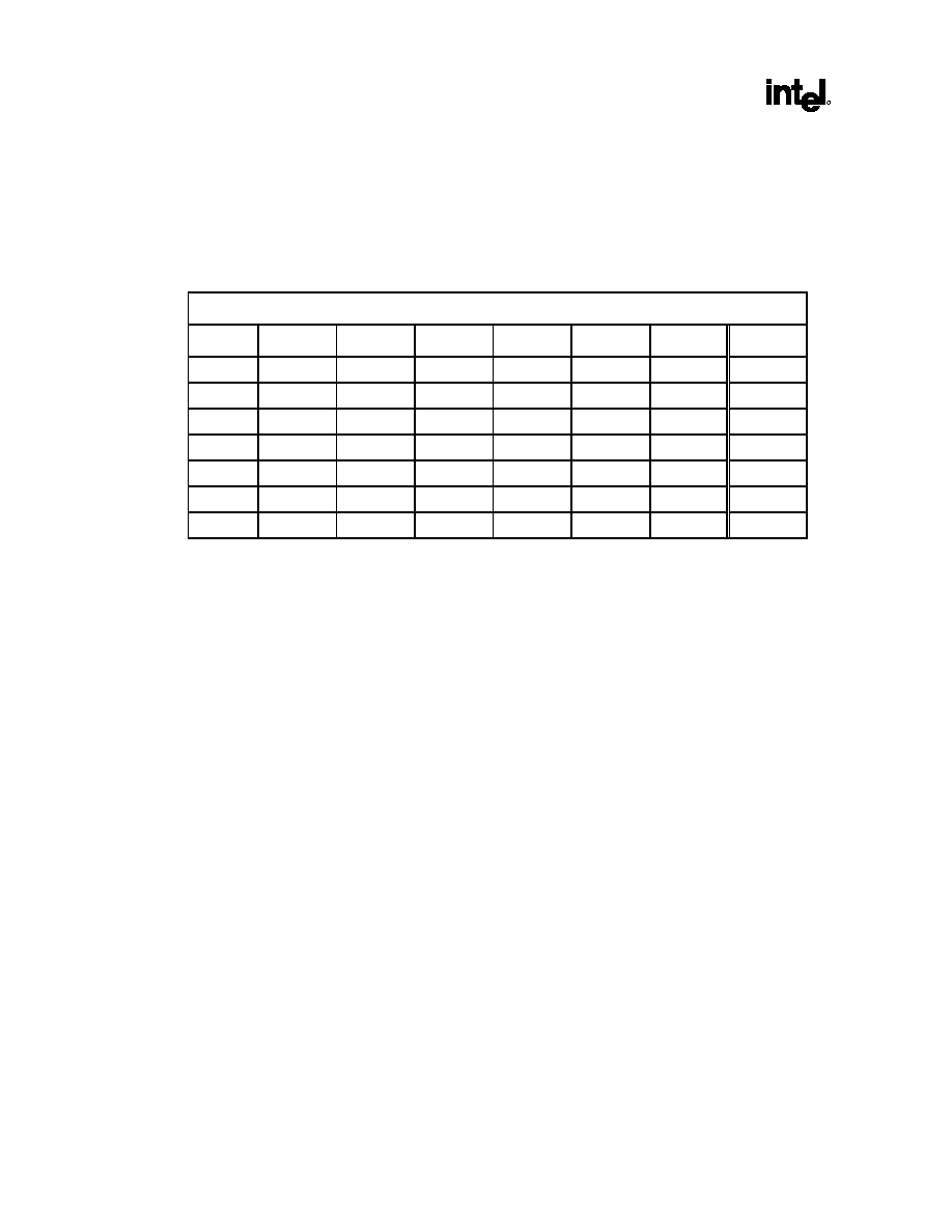
82815EP and 82815P MCH
R
130
Datasheet
6.1. XOR Tree Testability Algorithm Example
XOR tree testing allows users to check, for example, opens and shorts to VCC or GND. An example
algorithm to do this is shown in Table 18.
Table 18. XOR Test Pattern Example
Pin # from Figure 11
Vector
PIN1 PIN2 PIN3 PIN4 PIN5 PIN6
XOROut
1 0 0 0 0 0 0 1
2 1 0 0 0 0 0 0
3 1 1 0 0 0 0 1
4 1 1 1 0 0 0 0
5 1 1 1 1 0 0 1
6 1 1 1 1 1 0 0
7 1 1 1 1 1 1 1
In this example, Vector 1 applies all 0s to the chain inputs. The outputs being non-inverting, will
consistently produce a 1 at the XOR chain output on a good board. One short to Vcc (or open floating to
Vcc) will cause a 0 at the chain output, signaling a defect.
Likewise, applying Vector 7 (all 1s) to chain inputs (given that there are an even number of signals in the
chain), will consistently produce a 1 at the XOR chain output on a good board. One short to Vss (or open
floating to Vss) will cause a 0 at the chain output, signaling a defect. It is important to note that the
number of inputs pulled to 1 will affect the expected chain output value. If the number chain inputs
pulled to 1 is even, then expect 1 at XOR-out; otherwise, if odd, expect 0.
Continuing to Illustrate with the example pattern in Table 18, as the pins are driven to 1 across the chain
in sequence, XOR-out will toggle between 0 and 1. Any break in the toggling sequence (e.g., 1011) will
identify the location of the short or open.
6.1.1.
Test Pattern Consideration for XOR Chains 3 and 4, and 7 and 8
Bi-directional pins HLPSTRB (chain 3) and HLPSTRB# (chain 4), and AGP strobes AD_STB0,
AD_STB1, and SB_STB (chain 7) and AD_STB0#, AD_STB1#, and SB_STB# (chain 8) must always
be complementary to each other. For example, if a 1 is driven on to HLPSTRB, a 0 must be driven on
HLPSTRB# and vice versa. This will need to be considered in applying test patterns to these chains.
Note that on platforms designed for the 82815EP device, XOR chains #3, #6, #7, and #8 cannot be
tested.

82815EP and 82815P MCH
R
Datasheet
131
6.2. XOR Tree Initialization
6.2.1.
Chain [1:6] Initialization
On chains [1:6], all that is required to prepare the device for XOR chain testing is to pull SRAS# low
prior to deasserting RESET#. The following sequence will put the MCH into XOR testability mode:
1. Deassert RESET# high and assert SRAS# low
2. Assert RESET# low; maintain SRAS# low
3. Deassert RESET# high; maintain SRAS# low
4. RESET# must be maintained high for the duration of testing.
No external clocking of the MCH is required for testing these chains. Note that on platforms designed for
the 82815EP device, XOR chains #3, #6, #7, and #8 cannot be tested.
6.2.2.
Chain [7:8] Initialization
On chains[7:8], all that is required to prepare the device for XOR chain testing is to pull SMAA2 low
prior to deasserting RESET#, then set LTVCK high and LTVDATA[11:6] to [101101] (1 means high
and 0 means low), follow other LTVCK high and LTVDATA[11:6] to [100011]. The following
sequence puts the MCH into XOR testability mode for Chain[7:8] only:
1. Deassert RESET# high and assert SMAA2 low
2. Assert RESET# low; maintain SMAA2 low
3. Deassert RESET# high; maintain SMAA2 low
4. Deassert LTVCK low and assert LTVDATA[11:6] to [101101]
5. Assert LTVCK high; maintain LTVDATA[11:6] to [101101]
6. Deassert LTVCK low; maintain LTVDATA[11:6] to [101101]
7. Deassert LTVCK low and assert LTVDATA[11:6] to [100011]
8. Assert LTVCK high; maintain LTVDATA[11:6] to [100011]
9. Deassert LTVCK low; maintain LTVDATA[11:6] to [100011]
10. RESET# must be maintained high for the duration of testing
No external clocking of the MCH is required for testing these chains. Note that on platforms designed for
the 82815EP device, XOR chains #3, #6, #7, and #8 cannot be tested.
82815EP and 82815P MCH
R
132
Datasheet
6.3. XOR Chain
This is the primary test mode for checking the IO buffer connectivity. There are a total of 8 XOR chains
each containing less than 65 XOR gates. The XOR gates are physically located in the IO buffers. This
test mode can be invoked with the use of reset straps.
Table 19 XOR Chain 1
35 Inputs
Output: SMAA5 (A12)
Pin Name
Ball
Voltage
Pin Name
Ball
Voltage
Pin Name
Ball
Voltage
DEFER#
M3
1.5V HD12#
AD2
1.5V HD30#
AD5
1.5V
HD0# AA1 1.5V
HD18# AE1 1.5V
HD9# AF3 1.5V
HA30# W5 1.5V
HD7# AC4 1.5V
HD16# AD6 1.5V
HD4#
AB1
1.5V HD13#
AD3
1.5V HD21#
AE5
1.5V
HD6# AA3 1.5V
HD23# AB5 1.5V
HD20# AF4 1.5V
HA26# AF6 1.5V
HD14# AF1 1.5V
HD24# AF5 1.5V
HD1# AB2 1.5V
HD2# AF2 1.5V
HD22# AC8 1.5V
HD15# AA4 1.5V
HD19# AB6 1.5V
HD26# AF6 1.5V
HD8# AC1 1.5V
HD3# AD4 1.5V
HD29# AD8 1.5V
HD5# AB3 1.5V
HD11# AE3 1.5V
HD28# AF8 1.5V
HD10#
AD1
1.5V HD31#
AB7
1.5V HD27#
AD11
1.5V
HD17# AC3 1.5V
HD25# AC6 1.5V
Table 20 XOR Chain 2
33 Inputs
Output: SMAA2 (F12)
Pin Name
Ball
Voltage
Pin Name
Ball
Voltage
Pin Name
Ball
Voltage
BPRI#
M5
1.5V HD38#
AF9
1.5V HD55#
AB13
1.5V
HD34#
AB8
1.5V HD45#
AF10
1.5V HD52#
AF13
1.5V
HD33#
AD7
1.5V HD41#
AB11
1.5V HD58#
AC14
1.5V
HD37#
AB9
1.5V HD49#
AE11
1.5V HD46#
AD14
1.5V
HD35#
AE7
1.5V HD63#
AC12
1.5V HD54#
AF14
1.5V
HD32#
AF7
1.5V HD51#
AF11
1.5V HD53#
AB14
1.5V
HD43#
AD9
1.5V HD47#
AD12
1.5V HD62#
AF15
1.5V
HD44#
AC10
1.5V HD48#
AB12
1.5V HD50#
AE15
1.5V
HD36#
AE9
1.5V HD40#
AF12
1.5V HD60#
AD15
1.5V
HD42#
AB10
1.5V HD59#
AD13
1.5V HD56#
AB15
1.5V
HD39#
AD10
1.5V HD57#
AE13
1.5V HD61#
AF16
1.5V

82815EP and 82815P MCH
R
Datasheet
133
Table 21 XOR Chain 3
38 Inputs
Output: SMAA0 (D13)
Pin
Name Ball Voltage Pin
Name Ball Voltage Pin
Name Ball Voltage
HL1 H26 1.8V
HA7# N5 1.5V
HA24# W4 1.5V
HL0 H24
1.8V
HA14#
P3 1.5V
HA27# Y3 1.5V
HLPSTRB G25 1.8V
HA8# P5
1.5V
CPURST# AA5 1.5V
HL5 E26 1.8V
HA3# R4 1.5V LTVHSYNC
AB17
1.8V
HL6 E25 1.8V
HA9# R1 1.5V
LTVCLKIN
AC18
1.8V
HL8 D25 1.8V
HA12#
T1 1.5V LTVDATA6
AF20
1.8V
ADS# G1 1.5V
HA13# T3 1.5V
LTVDATA9
AF21
1.8V
HTRDY# K3
1.5V
HA10# U1 1.5V
LTVDATA7 AD20 1.8V
DRDY# J1 1.5V
HA21# AE5 1.5V
LTVBLANK#
AB19 1.8V
RS0# K2 1.5V
HA22# AC8 1.5V
LTVDATA10
AE21
1.8V
HIT# K1 1.5V
HA19# AB6 1.5V
LTVDATA8
AC20
1.8V
HREQ2# M2 1.5V
HA23# W3 1.5V
LTVDATA11 AD21 1.8V
HREQ0# M1 1.5V
HA17# V5
1.5V
Note that on platforms designed for the 82815EP device, XOR chains #3, #6, #7, and #8 cannot be
tested.
Table 22 XOR Chain 4
36 Inputs
Output: SMAA9 (D13)
Pin Name
Ball
Voltage
Pin Name
Ball
Voltage
Pin Name
Ball
Voltage
HL2 H25
1.8V HREQ4#
N3
1.5V
HA18# Y2 1.5V
HL3 G24
1.8V HREQ1#
N1
1.5V LTVDATA0
AD16
1.8V
HLPSTRB# F26 1.8V
HA11# P2 1.5V
LTVVSYNC AC16 1.8V
HL4 F24
1.8V
HA4#
P1
1.5V LTVDATA1
AF17
1.8V
HL7 D26
1.8V
HA6#
R3
1.5V LTVDATA2
AE17
1.8V
HL10 C26
1.8V
HA16#
AD6
1.5V
LTVDATA3
AD17
1.8V
DBSY# J3 1.5V
HA5# T2 1.5V
LTVDATA4 AF18
1.8V
RS2# H1 1.5V
HA15#
T5
1.5V
LTVDATA5
AD18
1.8V
HLOCK# L4 1.5V
HA28# U3 1.5V
LTVCLKOUT1
AF19 1.8V
HREQ3# L5 1.5V
HA31# V1 1.5V
LTVCLKOUT0
AE19 1.8V
HITM# L3 1.5V
HA25#
U5
1.5V
HA20# W1 1.5V
RS1# L1 1.5V
BNR# N4
1.5V
HA29# Y1 1.5V

82815EP and 82815P MCH
R
134
Datasheet
Table 23 XOR Chain 5
56 Inputs
Output: SMD31 (K5)
Pin Name
Ball
Voltage
Pin Name
Ball
Voltage
Pin Name
Ball
Voltage
SBS1 D11
3.3V
SCKE5
C7
3.3V
SMD59 F4 3.3V
SMAA10 E11 3.3V
SCKE3 D7 3.3V
SMD50 B1 3.3V
SMAC5# A10 3.3V
SMD39 A22 3.3V
SMD58 E3 3.3V
SMAC4# B10 3.3V
SDQM7 A5 3.3V
SMD57 D2 3.3V
SMAC6# C10 3.3V
SMD53 E6 3.3V
SMD62 H4 3.3V
SMAC7# A9 3.3V
SMD54 D5 3.3V
SMD63 J4 3.3V
SMAA12 B7 3.3V
SMD48 A4 3.3V
SMD51 E1 3.3V
SDQM6 B6 3.3V
SMD55 C4 3.3V
SMD52 G2 3.3V
SCKE4 C8 3.3V
SMD60 F6 3.3V
SCSA2# D14 3.3V
SMAB4# B15 3.3V
SMD56 B3 3.3V
SMAB6# C14 3.3V
SMD36 B23 3.3V
SMD49 A2 3.3V
SMAB5# A15 3.3V
SMD35 A24 3.3V
SMD61 G5 3.3V
SMAB7# A14 3.3V
VSYNC AF22 3.3V
SDQM5 C17
3.3V
SCSA4# E13 3.3V
SMD32 A26 3.3V
SCSA5# B17
3.3V
SMD37 A23 3.3V
SMD41 B21 3.3V
SDQM4 A18
3.3V
SMD34 B24 3.3V
SMD42 A21 3.3V
SMD46 C19
3.3V
SMD33 A25 3.3V
SCSA0# D15 3.3V
SMD45 A20 3.3V
SMD40 D21 3.3V
SCSA1# A17 3.3V
SMD47 A19 3.3V
SMD38 C22 3.3V
SCSA3# E14 3.3V
SMD43 C20 3.3V

82815EP and 82815P MCH
R
Datasheet
135
Table 24 XOR Chain 6
60 Inputs
Output: SMAA11 (A13)
Pin Name
Ball
Voltage
Pin Name
Ball
Voltage
Pin Name
Ball
Voltage
LOCLK R22 3.3V
SMD11 E18
3.3V
SRAS# C16 3.3V
LRCLK P22 3.3V
SMD10 D19
3.3V
SMAA1 B16 3.3V
SMD3 F21 3.3V
SMD13 F18
3.3V
SMAA3 A16 3.3V
SMD0 D23 3.3V
SMD44 B20
3.3V
SBS0 B13 3.3V
SMD5 G20 3.3V
SCAS# D18
3.3V
LTVCK AB21
3.3V
SMD6 F20 3.3V
SMD15 D17
3.3V
LTVDA AA20
3.3V
SMD4 E21 3.3V
SWE# E16
3.3V
DDCK AB18
3.3V
SMD2 D22 3.3V
SMD12 B18
3.3V
DDDA AA18
3.3V
SMD1 C23 3.3V
SDQM1
F15
3.3V
HSYNC AF23
3.3V
SMD8 F19 3.3V
SDQM0
D16
3.3V
SMD19 F2 3.3V
SMD9 E19 3.3V
SMD27 E4 3.3V
SMD30 J6 3.3V
SMD7 D20 3.3V
SMD25 C2 3.3V
SMD20 G3 3.3V
SMD14 G18 3.3V
SMD29 G4 3.3V
SCSB1# F8 3.3V
SCSB4# B9 3.3V
SMD24 D4 3.3V
SDQM2 A7 3.3V
SCSB3# D9 3.3V
SMD28 F5 3.3V
SCKE0 D8 3.3V
SCSB5# A8 3.3V
SMD26 D3 3.3V
SCKE1 E8 3.3V
SCKE2 E9 3.3V
SMD17 A1 3.3V
SDQM3 A6 3.3V
SMAA7 A11 3.3V
SMD18 C1 3.3V
SMD21 D6 3.3V
SMAA6 C11 3.3V
SMD23 B4 3.3V
SMD22 C5 3.3V
SCSB2# D10 3.3V
SMD16 A3 3.3V
SCSB0# F9 3.3V
Note that on platforms designed for the 82815EP device, XOR chains #3, #6, #7, and #8 cannot be
tested.

82815EP and 82815P MCH
R
136
Datasheet
Table 25 XOR Chain 7
33 Inputs
Output: SMAA8 (D12)
Pin Name
Ball
Voltage
Pin Name
Ball
Voltage
Pin Name
Ball
Voltage
ST2 AC23
Vddq GAD25
V21
Vddq
G_STOP#
P25
Vddq
ST0 AD24
Vddq G_AD28
W24
Vddq
G_AD14 N22
Vddq
G_GNT# AD25 Vddq
G_AD22 V24 Vddq
G_AD13 N24 Vddq
RBF# AD26
Vddq AD_STB1
U22
Vddq
G_AD11 M26 Vddq
PIPE# AC26
Vddq
G_AD26
V26
Vddq
G_AD9 M25 Vddq
SBA4 AA22 Vddq
G_AD17 T22 Vddq
AD_STB0 M22 Vddq
SB_STB Y23 Vddq
G_AD21 T24 Vddq
G_AD4 L24 Vddq
SBA3 AB26 Vddq
G_AD18 U24 Vddq
G_AD7 K23 Vddq
SBA5 AA26
Vddq G_C/BE2#
T25
Vddq
G_AD1 J22 Vddq
G_C/BE3# Y26 Vddq
G_PAR R24 Vddq
G_AD3
J21 Vddq
G_AD27 W21 Vddq
G_TRDY#
P21 Vddq
G_C/BE0# H23 Vddq
Note that on platforms designed for the 82815EP device, XOR chains #3, #6, #7, and #8 cannot be
tested.
Table 26 XOR Chain 8
31 Inputs
Output: SMAA4 (B12)
Pin Name
Ball
Voltage
Pin Name
Ball
Voltage
Pin Name
Ball
Voltage
ST1 AC24 Vddq
G_AD30 W26
Vddq
G_AD23 U21 Vddq
G_REQ# AE26 Vddq
AD_STB1# V23 Vddq
G_AD12 M21 Vddq
WBF# AB24 Vddq
G_AD24 V25
Vddq
G_AD10 M24 Vddq
SBA0 AB22
Vddq
G_AD19 T23
Vddq
G_AD8 K22 Vddq
SBA2 AB23
Vddq
G_AD20 U26
Vddq AD_STB0#
L23 Vddq
SBA6 Y22 Vddq
G_AD16 T26
Vddq
G_AD6 L26 Vddq
SB_STB# AA24 Vddq
G_IRDY# P23 Vddq
G_AD2 K25 Vddq
SBA1 AB25
Vddq G_FRAME#
R26
Vddq
G_AD5 J20 Vddq
SBA7 Y25 Vddq G_DEVSEL#
P26
Vddq
G_AD0 K26 Vddq
G_AD29 W22 Vddq
G_C/BE1# N21
Vddq
G_AD31 Y21 Vddq
G_AD15 N26
Vddq

82815EP and 82815P MCH
R
Datasheet
137
6.4. All Z
To apply vectors to XOR chains on a system board, other chips on the board must be tri-stated to allow
for this vector application. This is a feature that enables all MCH outputs to be tristated when the I/O
Controller Hub is in the XOR chain mode. This mode can also be activate using the assigned reset strap.
Tri-state MCH Outputs
When testing other devices in the system, the MCH outputs can be tri-stated. To tri-state these outputs
pull the SMAA10 pin low (GND) prior to deasserting RESET#. The following sequence will put the
MCH into tri-state mode:
1. 1. Deassert RESET# high and SMAA10 low
2. 2. Assert RESET# low; maintain SMAA10 low
3. 3. Deassert RESET# high; maintain SMAA10 low
4. 4. RESET# must be maintained high for the duration of testing.
No external clocking of the MCH is required.