 | –≠–Ľ–Ķ–ļ—ā—Ä–ĺ–Ĺ–Ĺ—č–Ļ –ļ–ĺ–ľ–Ņ–ĺ–Ĺ–Ķ–Ĺ—ā: 82870P2 | –°–ļ–į—á–į—ā—Ć:  PDF PDF  ZIP ZIP |
Document Outline
- Contents
- 1 Introduction 17
- Tables
- Revision History
- Introduction
- Signal Description
- Register Description
-
- Register Nomenclature and Access Attributes
- Hub Interface-to-PCI Bridge PCI Configuration Registers (Device 31 and 29)
- VIDĄVendor ID Register (D29,31: F0)
- DIDĄDevice ID Register (D29,31: F0)
- PD_CMDĄPCI Primary Device Command Register �(D29,31: F0)
- PD_STSĄPCI Primary Device Status Register (D29,31: F0)
- RIDĄRevision ID Register (D29,31: F0)
- CCĄClass Code Register (D29,31: F0)
- CLSĄCache Line Size Register (D29,31: F0)
- PMLTĄPrimary Master Latency Timer Register �(D29,31: F0)
- HEADTYPĄHeader Type Register (D29,31: F0)
- BNUMĄBus Number Register (D29,31: F0)
- SMLTĄSecondary Master Latency Timer (D29,31: F0)
- IOBL_ADRĄI/O Base and Limit Address Register �D29,31: F04
- SECSTSĄSecondary Status Register (D29,31: F0)
- MBL_ADRĄMemory Base and Limit Address Register (D29,31: F0)
- PMBL_ADRĄPrefetchable Memory Base and Limit Address Register (D29,31: F0)
- PREF_MEM_BASE_UPPERĄPrefetchable Memory Base Upper 32 Bit Address Register (D29,31: F0)
- PREF_MEM_LIM_UPPERĄPrefetchable Memory Limit Upper 32 Bit Address Register (D29,31: F0)
- IOBLU16_ADRĄI/O Base and Limit Upper 16 Bit Address Register (D29,31: F0)
- CAPPĄCapabilities List Pointer Register (D29,31: F0)
- INTRĄInterrupt Information Register (D29,31: F0)
- BRIDGE_CNTĄBridge Control Register (D31: F0)
- CNFĄP64H2 Configuration Register (D29,31: F0)
- MTTĄMulti-Transaction Timer Register (D29,31: F0)
- STRPĄPCI Strap Status Register (D29,31: F0)
- PX_CAPIDĄPCI-X Capabilities Identifier Register �(D29,31: F0)
- PX_SSTSĄPCI-X Secondary Status Register (D29,31: F0)
- PX_BSTSĄPCI-X Bridge Status Register (D29,31: F0)
- PX_USTCĄPCI-X Upstream Split Transaction Control Register (D29,31: F0)
- PX_DSTCĄPCI-X Downstream Split Transaction Control Register (D29,31: F0)
- RAS_STSĄRAS Status Register (D29,31: F0)
- RAS_DIĄRAS Data Integrity Codes Register (D29,31: F0)
- RAS_PHĄRAS PCI Header Register (D29,31: F0)
- RAS_PALĄRAS PCI Address Low Register (D29,31: F0)
- RAS_PAHĄRAS PCI Address High Register (D29,31: F0)
- RAS_PDLĄRAS PCI Data Low 32 Bits Register �(D29,31: F0)
- RAS_PDHĄRAS PCI Data High 32 bits Register �(D29,31: F0)
- RAS_HHĄRAS Hub Interface Header Register (D29,31: F0)
- RAS_HALĄRAS Hub Interface Address Low 32 Bits Register (D29,31: F0)
- RAS_HAHĄRAS Hub Interface Address High 32 Bits Register (D29,31: F0)
- RAS_HPĄRAS Hub Interface Prefetch Horizon Register (D29,31: F0)
- RAS_D0ĄRAS Hub Interface DWord 0 Register �(D29,31: F0)
- RAS_D1ĄRAS Hub Interface DWord 1 Register �(D29,31: F0)
- RAS_D2ĄRAS Hub Interface DWord 2 Register �(D29,31: F0)
- RAS_D3ĄRAS Hub Interface DWord 3 Register �(D29,31: F0)
- ACNFĄAdditional P64H2 Configuration Register �(D29,31: F0)
- PCCĄPCI Delay Compensation Control Register �(D29,31: F0)
- HCCRĄHub Interface Command/Control Register �(D29,31: F0)
- Prefetch Control Registers
- Hot Plug Controller Registers (Device 31)
- I/OxAPIC Interrupt Controller Registers
- PCI Configuration Space Registers (Device 28 and 30)
- VIDĄVendor ID Register (D28,30: F0)
- DIDĄDevice ID Register (D28,30: F0)
- PCICMDĄPCI Device Command Register (D28,30: F0)
- PCISTSĄPCI Device Status Register (D28,30: F0)
- RIDĄRevision ID Register (D28,30: F0)
- CCĄClass Code Register (D28,30: F0)
- HDRĄHeader (D28,30: F0)
- MBARĄMemory Base Register (D28,30: F0)
- SSĄSubsystem Identifier Register (D28,30: F0)
- CAP_PTRĄCapabilities Pointer Register (D28,30: F0)
- ABARĄAlternate Base Address Register (D28,30: F0)
- XIDĄPCI-X Identifier Register (D28,30: F0)
- XCRĄPCI-X Command Register (D28,30: F0)
- XSRĄPCI-X Status Register (D28,30: F0)
- Direct Memory Space Registers
- Indirect Memory Space Registers
- SMBus Interface
- Functional Description
- Electrical Characteristics
- Ballout and Package Information
- Testability

Intel
ģ
82870P2 PCI/PCI-X 64-bit
Hub 2 (P64H2)
Datasheet
January 2003
Document Number:
290732-002
R

R
2
Intel
ģ
82870P2 P64H2 Datasheet
Information in this document is provided in connection with Intel
ģ
products. No license, express or implied, by estoppel or otherwise, to any intellectual
property rights is granted by this document. Except as provided in Intel's Terms and Conditions of Sale for such products, Intel assumes no liability
whatsoever, and Intel disclaims any express or implied warranty, relating to sale and/or use of Intel products including liability or warranties relating to
fitness for a particular purpose, merchantability, or infringement of any patent, copyright or other intellectual property right. Intel products are not
intended for use in medical, life saving, or life sustaining applications.
Intel may make changes to specifications and product descriptions at any time, without notice.
Designers must not rely on the absence or characteristics of any features or instructions marked "reserved" or "undefined." Intel reserves these for
future definition and shall have no responsibility whatsoever for conflicts or incompatibilities arising from future changes to them.
The Intel
ģ
PCI/PCI-X 64-bit Hub 2 (P64H2) may contain design defects or errors known as errata which may cause the product to deviate from
published specifications. Current characterized errata are available on request.
Contact your local Intel sales office or your distributor to obtain the latest specifications and before placing your product order.
Copies of documents which have an ordering number and are referenced in this document, or other Intel literature, may be obtained from:
Intel Corporation
www.intel.com
or call 1-800-548-4725
Intel and the Intel logo are trademarks or registered trademarks of Intel Corporation or its subsidiaries in the United States and other countries.
*Other names and brands may be claimed as the property of others.
Copyright © 2003, Intel Corporation

R
Intel
ģ
82870P2 P64H2 Datasheet 3
Contents
1
Introduction ....................................................................................................................... 17
1.1
Related Documents.............................................................................................. 17
1.2
Intel
ģ
P64H2 Overview ......................................................................................... 17
2
Signal Description ............................................................................................................. 19
2.1
Hub Interface........................................................................................................ 21
2.2
PCI Bus Interface 64-bit Extension ...................................................................... 25
2.3
PCI Bus Interface Clocks and Reset.................................................................... 27
2.4
Interrupt Interface ................................................................................................. 28
2.5
Hot Plug Interface................................................................................................. 29
2.6
SMBus Interface................................................................................................... 31
2.7
Miscellaneous Signals.......................................................................................... 31
2.8
Power and Reference Voltage Signals
................................................................. 32
2.9
Pin Straps............................................................................................................. 32
3
Register Description.......................................................................................................... 34
3.1
Register Nomenclature and Access Attributes..................................................... 35
3.2
Hub Interface-to-PCI Bridge PCI Configuration Registers (Device 31 and 29).... 36
3.2.1
VID--Vendor ID Register (D29,31: F0) ................................................ 38
3.2.2
DID--Device ID Register (D29,31: F0)................................................. 38
3.2.3
PD_CMD--PCI Primary Device Command Register (D29,31: F0) ..... 38
3.2.4
PD_STS--PCI Primary Device Status Register (D29,31: F0) .............. 40
3.2.5
RID--Revision ID Register (D29,31: F0) .............................................. 41
3.2.6
CC--Class Code Register (D29,31: F0)............................................... 41
3.2.7
CLS--Cache Line Size Register (D29,31: F0) ..................................... 42
3.2.8
PMLT--Primary Master Latency Timer Register (D29,31: F0)............ 42
3.2.9
HEADTYP--Header Type Register (D29,31: F0)................................. 42
3.2.10
BNUM--Bus Number Register (D29,31: F0)........................................ 43
3.2.11
SMLT--Secondary Master Latency Timer (D29,31: F0) ...................... 43
3.2.12
IOBL_ADR--I/O Base and Limit Address Register D29,31: F04 ........ 44
3.2.13
SECSTS--Secondary Status Register (D29,31: F0)............................ 44
3.2.14
MBL_ADR--Memory Base and Limit Address Register (D29,31: F0) . 46
3.2.15
PMBL_ADR--Prefetchable Memory Base and Limit Address
Register (D29,31: F0) ........................................................................... 46
3.2.16
PREF_MEM_BASE_UPPER--Prefetchable Memory Base
Upper 32 Bit Address Register (D29,31: F0) ........................................ 47
3.2.17
PREF_MEM_LIM_UPPER--Prefetchable Memory Limit
Upper 32 Bit Address Register (D29,31: F0) ........................................ 47
3.2.18
IOBLU16_ADR--I/O Base and Limit Upper 16 Bit Address
Register (D29,31: F0) ........................................................................... 47
3.2.19
CAPP--Capabilities List Pointer Register (D29,31: F0) ....................... 48
3.2.20
INTR--Interrupt Information Register (D29,31: F0).............................. 48
3.2.21
BRIDGE_CNT--Bridge Control Register (D31: F0) ............................. 48
3.2.22
CNF--P64H2 Configuration Register (D29,31: F0).............................. 51
3.2.23
MTT--Multi-Transaction Timer Register (D29,31: F0) ......................... 52

R
4
Intel
ģ
82870P2 P64H2 Datasheet
3.2.24
STRP--PCI Strap Status Register (D29,31: F0) .................................. 52
3.2.25
PX_CAPID--PCI-X Capabilities Identifier Register (D29,31: F0)........ 53
3.2.26
PX_SSTS--PCI-X Secondary Status Register (D29,31: F0) ............... 53
3.2.27
PX_BSTS--PCI-X Bridge Status Register (D29,31: F0) ...................... 54
3.2.28
PX_USTC--PCI-X Upstream Split Transaction Control
Register (D29,31: F0) ........................................................................... 55
3.2.29
PX_DSTC--PCI-X Downstream Split Transaction Control
Register (D29,31: F0) ........................................................................... 55
3.2.30
RAS_STS--RAS Status Register (D29,31: F0).................................... 56
3.2.31
RAS_DI--RAS Data Integrity Codes Register (D29,31: F0) ................ 59
3.2.32
RAS_PH--RAS PCI Header Register (D29,31: F0) ............................. 59
3.2.33
RAS_PAL--RAS PCI Address Low Register (D29,31: F0) .................. 60
3.2.34
RAS_PAH--RAS PCI Address High Register (D29,31: F0)................. 60
3.2.35
RAS_PDL--RAS PCI Data Low 32 Bits Register (D29,31: F0)........... 60
3.2.36
RAS_PDH--RAS PCI Data High 32 bits Register (D29,31: F0).......... 61
3.2.37
RAS_HH--RAS Hub Interface Header Register (D29,31: F0) ............. 61
3.2.38
RAS_HAL--RAS Hub Interface Address Low 32 Bits
Register (D29,31: F0) ........................................................................... 61
3.2.39
RAS_HAH--RAS Hub Interface Address High 32 Bits
Register (D29,31: F0) ........................................................................... 62
3.2.40
RAS_HP--RAS Hub Interface Prefetch Horizon Register (D29,31: F0)62
3.2.41
RAS_D0--RAS Hub Interface DWord 0 Register (D29,31: F0) .......... 62
3.2.42
RAS_D1--RAS Hub Interface DWord 1 Register (D29,31: F0) .......... 63
3.2.43
RAS_D2--RAS Hub Interface DWord 2 Register (D29,31: F0) .......... 63
3.2.44
RAS_D3--RAS Hub Interface DWord 3 Register (D29,31: F0) .......... 63
3.2.45
ACNF--Additional P64H2 Configuration Register (D29,31: F0).......... 64
3.2.46
PCC--PCI Delay Compensation Control Register (D29,31: F0) ......... 66
3.2.47
HCCR--Hub Interface Command/Control Register (D29,31: F0) ....... 67
3.2.48
Prefetch Control Registers.................................................................... 68
3.2.48.1
PC33--Prefetch Control for 33 MHz
Register (D29,31: F0).......................................................... 68
3.2.48.2
PC66--Prefetch Control for 66 MHz
Register (D29,31: F0).......................................................... 68
3.2.48.3
PC100--Prefetch Control for 100 MHz
Register (D29,31: F0).......................................................... 69
3.2.48.4
PC133--Prefetch Control for 133 MHz
Register (D29,31: F0).......................................................... 69
3.3
Hot Plug Controller Registers (Device 31) ........................................................... 70
3.3.1
PCI Configuration Registers ................................................................. 70
3.3.1.1
VID--Vendor ID Register (Device 31)................................. 71
3.3.1.2
DID--Device ID Register (Device 31) ................................. 71
3.3.1.3
PCICMD--PCI Command Register (Device 31) ................. 71
3.3.1.4
PCISTS--PCI Status Register (Device 31)......................... 72
3.3.1.5
RID--Revision ID Register (Device 31) .............................. 72
3.3.1.6
CC--Class Code Register (Device 31) ............................... 73
3.3.1.7
MBAR--Memory Base Register (Device 31) ...................... 73
3.3.1.8
MBARU--Memory Base Address (Upper 32-bits)
Register (Device 31)............................................................ 73
3.3.1.9
SVID--Subsystem Vendor ID Register (Device 31)............ 74
3.3.1.10
SID--Subsystem ID Register (Device 31)........................... 74
3.3.1.11
CAP_PTR--Capabilities Pointer Register (Device 31) ....... 74
3.3.1.12
INTR--Interrupt Information Register (Device 31) .............. 75
3.3.1.13
SID--Slot ID Register (Device 31) ...................................... 75

R
Intel
ģ
82870P2 P64H2 Datasheet 5
3.3.1.14
HPFC--Hot Plug Frequency Control Register
(Device 31) .......................................................................... 75
3.3.1.15
MCNF--Miscellaneous Configuration Register
(Device 31) .......................................................................... 76
3.3.1.16
FTR--Features Register (Device 31).................................. 78
3.3.1.17
SSEL--Slot Status Select Register (Device 31) ................. 78
3.3.1.18
SSTS--Slot Status Register (Device 31) ............................ 79
3.3.1.19
SERR--SERR Status Register (Device 31)........................ 80
3.3.1.20
MIDX--Alternate Memory Access Index Port Register
(Device 31) .......................................................................... 80
3.3.1.21
MDTA--Alternate Memory Access Data Port Register
(Device 31) .......................................................................... 81
3.3.1.22
XID--PCI-X Identifiers Register (Device 31)....................... 81
3.3.1.23
XCR--PCI-X Command Register (Device 31) .................... 81
3.3.1.24
XSR--PCI-X Status Register (Device 31)........................... 82
3.3.1.25
ABAR--Alternate Base Register (Device 31)...................... 82
3.3.2
Memory Space Registers ..................................................................... 83
3.3.2.1
GPT--General Purpose Timer Register ............................. 84
3.3.2.2
SE--Slot Enable Register ................................................... 84
3.3.2.3
MCNF--Miscellaneous Configuration Register................... 85
3.3.2.4
LEDC--LED Control Register ............................................. 87
3.3.2.5
HMIC--Hot Plug Interrupt Input and Clear Register ........... 88
3.3.2.6
HMIR--Hot Plug Interrupt Mask Register ........................... 89
3.3.2.7
SIR--Serial Input Register .................................................. 90
3.3.2.8
GPO--General Purpose Output Register ........................... 90
3.3.2.9
HMIN--Hot Plug Non-Interrupt Inputs Register .................. 91
3.3.2.10
SID--Slot ID Register.......................................................... 91
3.3.2.11
SIRE--Switch Interrupt Redirect Enable Register .............. 91
3.3.2.12
SPE--Slot Power Enable Register...................................... 92
3.3.2.13
EMR--Extended Hot Plug Miscellaneous Register............. 93
3.4
I/OxAPIC Interrupt Controller Registers ............................................................... 94
3.4.1
PCI Configuration Space Registers (Device 28 and 30)....................... 94
3.4.1.1
VID--Vendor ID Register (D28,30: F0) ............................... 95
3.4.1.2
DID--Device ID Register (D28,30: F0) ............................... 95
3.4.1.3
PCICMD--PCI Device Command Register (D28,30: F0) ... 96
3.4.1.4
PCISTS--PCI Device Status Register (D28,30: F0) ........... 97
3.4.1.5
RID--Revision ID Register (D28,30: F0)............................. 97
3.4.1.6
CC--Class Code Register (D28,30: F0) ............................. 98
3.4.1.7
HDR--Header (D28,30: F0) ................................................ 98
3.4.1.8
MBAR--Memory Base Register (D28,30: F0)..................... 98
3.4.1.9
SS--Subsystem Identifier Register (D28,30: F0)................ 99
3.4.1.10
CAP_PTR--Capabilities Pointer Register (D28,30: F0)...... 99
3.4.1.11
ABAR--Alternate Base Address Register (D28,30: F0)...... 99
3.4.1.12
XID--PCI-X Identifier Register (D28,30: F0)..................... 100
3.4.1.13
XCR--PCI-X Command Register (D28,30: F0) ................ 100
3.4.1.14
XSR--PCI-X Status Register (D28,30: F0) ....................... 100
3.4.2
Direct Memory Space Registers ......................................................... 101
3.4.2.1
IDX--Index Register (D28,30: F0) .................................... 101
3.4.2.2
WND--Window Register (D28,30: F0) ............................. 101
3.4.2.3
PAR--IRQ Pin Assertion Register (D28,30: F0) ............... 102
3.4.2.4
EOI--End of Interrupt Register (D28,30: F0) .................... 102

R
6
Intel
ģ
82870P2 P64H2 Datasheet
3.4.3
Indirect Memory Space Registers....................................................... 103
3.4.3.1
ID--APIC ID Register (D28,30: F0)................................... 103
3.4.3.2
VS--Version Register (D28,30: F0) .................................. 104
3.4.3.3
ARBID--Arbitration ID Register (D28,30: F0) ................... 104
3.4.3.4
BCFG--Boot Configuration Register (D28,30: F0) ........... 105
3.4.3.5
RDL--Redirection Table Low DWord Register
(D28,30: F0) ...................................................................... 105
3.4.3.6
RDH--Redirection Table High Register (D28,30: F0)....... 106
3.5
SMBus Interface................................................................................................. 107
3.5.1
CMDSTS--Command / Status Register............................................. 108
3.5.2
BNUM--Bus Number Register ........................................................... 109
3.5.2.1
DFNUM--Device / Function Number Register.................. 109
3.5.3
RNUM--Register Number .................................................................. 109
3.5.3.1
DATA--Data Register ....................................................... 110
3.5.4
CFG--SMBus Configuration Register ................................................ 110
4
Functional Description .................................................................................................... 112
4.1
PCI Interface ...................................................................................................... 112
4.1.1
Summary of Changes ......................................................................... 112
4.1.2
Transaction Types .............................................................................. 113
4.1.3
Detection of 64-bit Environment ......................................................... 113
4.1.4
Data Bus ............................................................................................. 114
4.1.5
Read Transactions.............................................................................. 115
4.1.6
Configuration Transactions................................................................. 115
4.1.7
Transaction Termination..................................................................... 118
4.1.8
Lock Cycles ........................................................................................ 119
4.1.9
Error Handling..................................................................................... 119
4.1.9.1
Address Parity Errors ........................................................ 120
4.1.9.2
Data Parity Errors .............................................................. 121
4.1.9.3
Hub Interface Configuration Write Transactions ............... 121
4.1.9.4
Read Transactions from Hub Interface Targeting PCI...... 121
4.1.9.5
Read Transactions from PCI Targeting Hub Interface...... 121
4.1.9.6
Write Transactions on Hub Interface
(Intel
ģ
P64H2 As Hub Interface Target) ............................ 122
4.1.9.7
Write Transactions on Hub Interface
(Intel
ģ
P64H2 As Hub Interface Master)............................ 122
4.1.9.8
Write Transactions on PCI
(Intel
ģ
P64H2 As PCI Target)............................................ 122
4.1.9.9
Write Transactions on PCI
(Intel
ģ
P64H2 As PCI Master) ........................................... 122
4.1.9.10
System Errors.................................................................... 123
4.1.9.11
PCI SERR# Pin Assertion ................................................. 123
4.1.9.12
Other System Errors.......................................................... 123
4.2
PCI-X Interface................................................................................................... 124
4.2.1
Command Encoding ........................................................................... 124
4.2.2
Attributes............................................................................................. 125
4.2.3
Burst Transactions.............................................................................. 125
4.2.4
Device Select Timing .......................................................................... 125
4.2.5
Wait States ......................................................................................... 126
4.2.6
Split Transactions ............................................................................... 126
4.2.6.1
Completer Attributes.......................................................... 126
4.2.6.2
Requirements for Accepting Split Completions................. 126
4.2.6.3
Split Completion Messages............................................... 126

R
Intel
ģ
82870P2 P64H2 Datasheet 7
4.2.7
Arbitration Among Multiple Split Completions..................................... 127
4.2.8
Transaction Termination as a PCI-X Target ....................................... 127
4.2.9
Arbitration ........................................................................................... 127
4.2.10
System Initialization ............................................................................ 128
4.2.11
Bridge Buffer Requirements ............................................................... 129
4.2.12
Cycle Translation Between Interfaces ................................................ 129
4.2.12.1
Conventional PCI to PCI-X / Hub Interface ....................... 129
4.2.12.2
PCI-X to Conventional PCI (peer) / Hub Interface............. 130
4.2.13
Locked Transactions .......................................................................... 130
4.2.14
Error Support ...................................................................................... 130
4.2.15
Transaction Termination Translation Between Interfaces .................. 130
4.2.15.1
Behavior of Hub Interface Initiated Cycles to
PCI/PCI-X Receiving Immediate Terminations ................. 131
4.2.15.2
Behavior of Hub Interface Initiated Cycles to
PCI-X Receiving Split Terminations .................................. 132
4.2.15.3
Hub Interface Action on Immediate Responses to
PCI-X Split Completions.................................................... 133
4.2.16
Configuration Transactions................................................................. 134
4.3
Hot Plug Controllers ........................................................................................... 135
4.3.1
System Architecture............................................................................ 135
4.3.1.1
Output Control ................................................................... 135
4.3.1.2
Input Control...................................................................... 136
4.3.1.3
Stutter Mode ...................................................................... 136
4.3.1.4
Serial Input Stream............................................................ 137
4.3.1.5
Serial Output Stream ......................................................... 140
4.3.1.6
Power Sequencing ............................................................ 143
4.3.1.7
Arbitration .......................................................................... 146
4.3.1.8
Power-on and Reset Initialization ...................................... 146
4.3.1.9
PCI Card Initialization ........................................................ 147
4.3.1.10
Changing PCI Frequency/Modes ...................................... 147
4.3.2
Pin Multiplexing in Single and Dual Slot Modes.................................. 148
4.3.3
Single Slot Mode PCI Bus Effects ...................................................... 150
4.3.3.1
Driving Bus To Ground When PCI Card is
Disconnected..................................................................... 150
4.3.3.2
Aborting Outbound PCI Cycles When Card is
Disconnected..................................................................... 151
4.3.3.3
Special Note on M66EN in Single Slot Mode .................... 151
4.3.4
Generating SCI Instead of Interrupt.................................................... 151
4.3.5
Disabling the Hot Plug Controller........................................................ 151
4.4
Addressing ......................................................................................................... 152
4.4.1
I/O Window Addressing ...................................................................... 152
4.4.2
Memory Window Addressing .............................................................. 153
4.4.2.1
Memory Base and Limit Address Registers ...................... 153
4.4.2.2
Prefetchable Memory Base and Limit Address
Registers, Upper 32-bit Registers .................................... 153
4.4.3
VGA Addressing ................................................................................. 154
4.4.4
Configuration Addressing ................................................................... 155

R
8
Intel
ģ
82870P2 P64H2 Datasheet
4.5
Transaction Ordering ......................................................................................... 156
4.5.1
Comparison of Rules vs A PCI≠PCI Bridge........................................ 156
4.5.2
Ordering Relationships ....................................................................... 156
4.5.3
Hub Interface Fence Special Cycle .................................................... 157
4.5.4
Master Abort / Target Abort Completions on Hub Interface ............... 157
4.5.4.1
Behavior of Hub Interface Initiated Cycles to
PCI/PCI-X Receiving Immediate Terminations ................. 157
4.5.4.2
Behavior of Hub Interface Initiated Cycles PCI-X
Receiving Split Terminations............................................. 158
4.5.4.3
Hub Interface Action on Immediate Responses to
PCI-X Split Completions.................................................... 159
4.5.4.4
Behavior of PCI/PCI-X Initiated Cycles to Hub Interface... 159
4.6
I/OxAPIC Interrupt Controller (Device 30 and 28) .............................................. 160
4.6.1
Interrupt Insertion................................................................................ 160
4.6.1.1
Pin Interrupts ..................................................................... 160
4.6.1.2
Message Signaled Interrupts (MSI)................................... 160
4.6.2
Interrupt Delivery................................................................................. 160
4.6.2.1
Front-Side Interrupt Delivery ............................................. 160
4.6.3
Buffer Flushing.................................................................................... 162
4.6.4
Boot Interrupt ...................................................................................... 162
4.7
SMBus Interface................................................................................................. 163
4.7.1
SMBus Signaling................................................................................. 163
4.7.1.1
Waveforms ........................................................................ 164
4.7.1.2
Architecture ....................................................................... 166
4.7.1.3
Data Transfer Examples ................................................... 168
4.7.1.4
Configuration Space Registers.......................................... 169
4.7.1.5
Memory Space Registers .................................................. 169
4.7.2
Configuration Access Arbitration ........................................................ 170
4.8
System Setup ..................................................................................................... 171
4.8.1
Clocking .............................................................................................. 171
4.8.2
Component Reset............................................................................... 172
4.8.2.1
Software PCI Reset........................................................... 172
4.8.2.2
RSTIN#.............................................................................. 173
4.8.2.3
PowerOK ........................................................................... 173
4.8.3
I/OxAPIC System Assumptions .......................................................... 174
4.9
Reliability, Availability, and Serviceability (RAS)................................................. 175
4.9.1
Error Types ......................................................................................... 176
4.9.2
Error Logging ...................................................................................... 176
4.9.3
Logged Errors ..................................................................................... 178
4.9.4
Allowable Error Combinations for RAS_STS...................................... 178
4.9.5
Data Poisoning ................................................................................... 179

R
Intel
ģ
82870P2 P64H2 Datasheet 9
5
Electrical Characteristics................................................................................................. 180
5.1
DC Voltage and Current Characteristics ............................................................ 180
5.1.1
Intel
ģ
P64H2 DC Characteristics ........................................................ 180
5.1.2
Input Characteristic Signal Association .............................................. 181
5.1.3
DC Input Characteristics..................................................................... 181
5.1.4
DC Characteristic Output Signal Association ..................................... 182
5.1.5
DC Output Characteristics .................................................................. 183
5.1.6
Other DC Characteristics.................................................................... 183
5.1.6.1
Hub Interface 2.0 DC Characteristics................................ 184
5.1.6.2
PCI Interface DC Characteristics
(5 V Signaling Environment).............................................. 185
5.1.6.3
PCI Interface DC Characteristics
(3.3 V Signaling Environment)........................................... 186
5.1.6.4
PCI-X Interface DC Characteristics................................... 186
5.1.6.5
PCI Hot Plug DC Characteristics....................................... 187
5.1.6.6
Input Clock DC Characteristics ......................................... 187
5.1.6.7
Output Clock DC Characteristics ...................................... 188
5.2
AC Characteristics and Timing........................................................................... 189
5.2.1
PCI Interface Timing ........................................................................... 189
5.2.1.1
PCI Clock Characteristics ................................................. 191
5.2.1.2
PCI Clock Uncertainty ....................................................... 192
5.2.2
PCI-X Interface Timing ....................................................................... 193
5.2.2.1
PCI-X Clock Characteristics.............................................. 195
5.2.2.2
PCI-X Clock Uncertainty.................................................... 196
5.2.2.3
P64H2 Clock Timings........................................................ 197
5.2.2.4
Spread Spectrum Clocking ............................................... 200
6
Ballout and Package Information .................................................................................... 201
6.1
Package Information .......................................................................................... 210
6.1.1
Package Trace Lengths for Hub Interface.......................................... 213
7
Testability ........................................................................................................................ 215
7.1
XOR Power Up Strap ......................................................................................... 215
7.2
XOR Test Chain Test ......................................................................................... 215
7.3
Pins Excluded from XOR Chain Testing ............................................................ 217

R
10
Intel
ģ
82870P2 P64H2 Datasheet
Figures
Figure 1. Intel
ģ
P64H2 Signal Block Diagram ................................................................... 20
Figure 2. Type 1 to Type 0 Translation ........................................................................... 116
Figure 3. Serial Input 6-slot Stutter Mode ....................................................................... 137
Figure 4. Intel P64H2 Appearance to Software .............................................................. 155
Figure 5. Basic SMBus Transfer Waveform ................................................................... 164
Figure 6. Start (S) / Repeat Start (Sr) Signaling ............................................................. 164
Figure 7. Stop (P) Signaling ............................................................................................ 164
Figure 8. ACK (A) Signaling ............................................................................................ 165
Figure 9. NACK (N) Signaling ......................................................................................... 165
Figure 10. Stack View of SMBus Register Space........................................................... 166
Figure 11. Flow Diagram for SMBus............................................................................... 167
Figure 12. Intel
ģ
P64H2 Busy ......................................................................................... 168
Figure 13. Intel
ģ
P64H2 Busy ......................................................................................... 168
Figure 14. Reading A Register........................................................................................ 169
Figure 15. 66 MHz PCLK Skew ...................................................................................... 172
Figure 16. PCI Output Timing ......................................................................................... 190
Figure 17. PCI Input Timing ............................................................................................ 190
Figure 18. PCI Clock Waveforms ................................................................................... 191
Figure 19. PCI Clock Skew ............................................................................................. 192
Figure 20. PCI-X Output Timing...................................................................................... 194
Figure 21. PCI-X Input Timing ........................................................................................ 194
Figure 22. PCI-X 3.3 V Clock Waveform ........................................................................ 195
Figure 23. PCI-X Clock Skew ......................................................................................... 196
Figure 24. Intel
ģ
P64H2 Ballout (Left Side)..................................................................... 202
Figure 25. Intel
ģ
P64H2 Ballout (Right Side) .................................................................. 203
Figure 26. 567-Ball FCBGA Package Dimensions (Top View) ....................................... 210
Figure 27. 567-Ball FCBGA Package Dimensions (Bottom View).................................. 211
Figure 28. 567-Ball FCBGA Solder Balls Detail .............................................................. 212

R
Intel
ģ
82870P2 P64H2 Datasheet 11
Tables
Table 1. Hub Interface ...................................................................................................... 21
Table 2. PCI Bus Interface A Signals................................................................................ 21
Table 3. PCI Bus Interface B Signals................................................................................ 23
Table 4. PCI Bus Interface 64-bit Extension Interface A Signals...................................... 25
Table 5. PCI Bus Interface 64-bit Extension Interface B Signals...................................... 26
Table 6. PCI Bus Interface Clocks and Reset Interface A Signals ................................... 27
Table 7. PCI Bus Interface Clocks and Reset Interface B Signals ................................... 27
Table 8. Interrupt Interface Signals................................................................................... 29
Table 9. Hot Plug Interface A Signals ............................................................................... 29
Table 10. Hot Plug Interface B Signals ............................................................................. 30
Table 11. SMBus Interface Signals................................................................................... 31
Table 12. Miscellaneous Signals ...................................................................................... 31
Table 13. Power and Reference Voltage Signals ............................................................. 32
Table 14. Normal Functional Pin Straps ........................................................................... 32
Table 15. Hub Interface-to-PCI Bridges Address Map (D31,29, F0) ................................ 36
Table 16. Hot Plug Controller PCI Configuration Address Map (Device 31)..................... 70
Table 17. Hot Plug Controller Memory Space Register Map ............................................ 83
Table 18. I/OxAPIC PCI Configuration Space Register Map ............................................ 94
Table 19. I/OxAPIC Memory Space Register Map ......................................................... 101
Table 20. I/OxAPIC Indirect Memory Space Register Address Map .............................. 103
Table 21. SMBus Register Address Map........................................................................ 107
Table 22. Intel
ģ
P64H2 PCI Transactions....................................................................... 113
Table 23. Command Encoding ....................................................................................... 124
Table 24. Intelģ P64H2 Implementation of Requester Attribute Fields .......................... 125
Table 25. DEVSEL# Timing ............................................................................................ 125
Table 26. Intel
ģ
P64H2 Implementation Completion Attribute Fields.............................. 126
Table 27. Split Completion Abort Registers .................................................................... 126
Table 28. M66EN and PCIXCAP Encoding .................................................................... 128
Table 29. PCI-X Initialization Pattern .............................................................................. 128
Table 30. Conventional PCI to PCI-X / Hub Interface..................................................... 129
Table 31.
PCI-X to Conventional PCI (peer) / Hub Interface .......................................... 130
Table 32. Immediate Terminations of Completion Required Cycles to PCI/PCI-X ......... 131
Table 33. Immediate Terminations of Posted Write Cycles to PCI/PCI-X ...................... 131
Table 34. Split Terminations of Completion Required Cycles to PCI-X .......................... 132
Table 35. Response to PCI-X Split Completions ............................................................ 133
Table 36. Terminations of Completion Requited Cycles to Hub Interface ...................... 133
Table 37. Stutter Logic Modes ........................................................................................ 136
Table 38. Shift Register Data.......................................................................................... 140
Table 39. Serial Mode Output Shift-Out SR Bit Order .................................................... 142
Table 40. Power Up Timings (CBF Mode) ...................................................................... 143
Table 41. Power Down Timings (CBF Mode) ................................................................. 144
Table 42. Power Up Timings (CBL Mode) ...................................................................... 145
Table 43. Power Down Timings (CBL Mode).................................................................. 146
Table 44. Registers Not Reset with a Secondary Bus Reset.......................................... 146
Table 45. Hot Plug Mode Settings .................................................................................. 148
Table 46. Hot Plug Mode Signals.................................................................................... 149
Table 47. Hot Plug Mode Reset Values .......................................................................... 149
Table 48. PCI Functions/Devices Table.......................................................................... 155
Table 49. Ordering Rules for a PCI-PCI Bridge .............................................................. 156
Table 50. Immediate Terminations of Completion Required Cycles to PCI/PCI-X ......... 157

R
12
Intel
ģ
82870P2 P64H2 Datasheet
Table 51. Immediate Terminations of Posted Write Cycles to PCI/PCI-X ...................... 158
Table 52. Split Terminations of Completion Required Cycles to PCI-X .......................... 158
Table 53. Hub Interface Response to PCI-X Split Completion Terminations of
Completion Required Cycles ................................................................................... 159
Table 54. Terminations of Completion Required Cycles to Hub Interface...................... 159
Table 55. System Bus Delivery Address Format ............................................................ 161
Table 56. System Bus Delivery Data Format .................................................................. 161
Table 57. SMBus Address Configuration........................................................................ 163
Table 58. P64H2 Clocking .............................................................................................. 171
Table 59. Determining PCI/PCI-X Bus Frequency.......................................................... 173
Table 60. Hot Plug Mode and Final Bus State ................................................................ 173
Table 61. RAS_STS Register (offset 60h) Values .......................................................... 179
Table 62. Intel
ģ
P64H2 DC Voltage Characteristics ....................................................... 180
Table 63. Intel
ģ
P64H2 DC Current Characteristics ....................................................... 180
Table 64.
DC Characteristics Input Signal Association .................................................. 181
Table 65.
DC Input Characteristics................................................................................. 181
Table 66.
DC Characteristic Output Signal Association ................................................. 182
Table 67.
DC Output Characteristics .............................................................................. 183
Table 68.
Other DC Characteristics................................................................................ 183
Table 69. DC Characteristics for Hub Interface Common Clock Signaling .................... 184
Table 70. DC Characteristics for Hub Interface Source Synchronous Signaling ............ 185
Table 71. DC Characteristics for PCI 5 V Signaling........................................................ 185
Table 72. DC Characteristics for PCI 3.3 V Signaling..................................................... 186
Table 73. DC Characteristics for PCI-X .......................................................................... 186
Table 74. PCI Hot Plug Slot Power Requirements ......................................................... 187
Table 75. DC Characteristics for Input Clock Signals..................................................... 187
Table 76. DC Characteristics for Output Clock Signals .................................................. 188
Table 77. PCI Interface Timing (HI_VREF = 5 V + 5%, VCC = 3.3 V + 5%, Tcase=0
į
C to
105
į
C)...................................................................................................................... 189
Table 78. PCI Clock Characteristics (HI_VREF = 5 V + 5%, VCC = 3.3 V + 5%,
Tcase=0
į
C to 105
į
C)............................................................................................. 191
Table 79. PCI Clock Skew Parameters (HI_VREF = 5 V + 5%, VCC = 3.3 V + 5%,
Tcase=0
į
C to 105
į
C)............................................................................................... 192
Table 80. PCI-X General Timing Parameters (HI_VREF = 5 V + 5%, VCC = 3.3 V + 5%,
Tcase=0
į
C to 105
į
C)............................................................................................... 193
Table 81. PCI-X Clock Timings (HI_VREF = 5 V + 5%, VCC = 3.3 V + 5%, Tcase=0
į
C to
105
į
C)...................................................................................................................... 195
Table 82. PCI-X Clock Uncertainty Parameters (HI_VREF = 5 V + 5%, VCC = 3.3 V
+ 5%, Tcase=0
į
C to 105
į
C) .................................................................................... 196
Table 83. P64H2 Clock Timings (HI_VREF = 5 V + 5%, VCC = 3.3 V + 5%, Tcase=0
į
C to
105
į
C)...................................................................................................................... 197
Table 84. Intel
ģ
P64H2 Ballout Listed Alphabetically by Signal Name............................ 204
Table 85. Intel
ģ
P64H2 Hub Interface Package Trace Lengths...................................... 213
Table 86. XOR Power Up Strap (Sampled during RESET) ............................................ 215
Table 87. XOR Chain Table (Chains 1≠6) ...................................................................... 215
Table 88. Pins Excluded from XOR Chain Testing......................................................... 217

R
Intel
ģ
82870P2 P64H2 Datasheet 13
Revision History
Revision Description
Date
-001
Initial Release.
February 2002
-002
Incorporated changes from P64H2 Spec Update Rev 001-007
January 2003

R
14
Intel
ģ
82870P2 P64H2 Datasheet
This page is intentionally left blank.

R
Intel
ģ
82870P2 P64H2 Datasheet 15
Intel
ģ
82870P2 P64H2 Features
Primary bus (the Hub Interface)
16 bit data interface
8x clock modes
64-bit and 32-bit addressing support
Parity/ECC Support
66 MHz base clock
Parallel Termination
Secondary bus (2 PCI Bus Interfaces)
PCI Specification, Revision 2.2 compliant
PCI-PCI Bridge Specification, Revision 1.1
compliant
PCI-X Specification, Revision 1.0 compliant
66 MHz 64bit, 3.3 V PCI bus (5 V Tolerant)
6 REQ/GNT per PCI bus segment (Internal
arbiter only)
Decoupled operation from Hub interface
64 bit addressing for inbound and outbound
transactions
Supports outbound LOCK# cycles
Fast Back-to-Back capable Bus parking on
Hub Interface
Bus parking on last PCI agent
Up to 4 active and 4 pending inbound
delayed transactions, and 1 outbound
delayed transaction per interface
Fair arbitration algorithm between each PCI
interface for ownership of Hub Interface
based upon the maximum bandwidth
requirements on each interface
PCI Bus B (with APIC B and Hot Plug
Controller B) can be hidden for a product
sku via a fuse
SMBus Interface
Full read/write access to all Configuration
and Memory registers
No accesses to PCI bus or Hub Interface
Hot Plug Controller
1 interface per PCI bus segment
Parallel support for 1 and 2 slot systems,
updates for PCI-X support.
Buffer Architecture (per interface)
4 KB of data, split into four 1024-byte
buffers, for inbound read requests from
PCI / PCI-X agents.
1.5 KB for inbound write transactions.
128 bytes for outbound read completions
16 outbound commands for completions and
requests.
16 inbound commands (posted and non-
posted)
I/O APIC
1 interface per PCI bus segment
Supports up to 24 interrupts (16 pins) per
interface
Serial interface for future PCG product
Compatible with both IA-32 and IA-64
Boot interrupt output
Test/Debug
Pilot Mode to monitor internals
Head-to-Head Mode to test two P64H2s tied
together with no MCH
Other features
Peer-to-peer memory writes between PCI
segments with fence ordering
Trapping of address / command for first
cycle with parity/ECC errors.
Parity protection of SRAM data
R
16
Intel
ģ
82870P2 P64H2 Datasheet
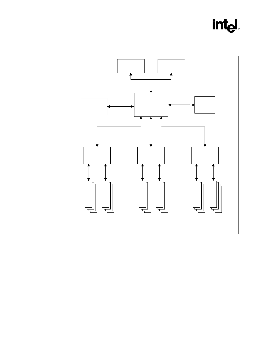
Intel
ģ
82870P2 P64H2 System Block Diagram
Sys_Blk
Processor
Processor
MCH
System
Memory
Intel
ģ
ICH3-S
P64H2
Intel
ģ
P64H2
P64H2
System Bus
16-Bit Hub
Interface
(1 GB/s)
8-Bit HI1.5
266 MB/s
PCI
or
PCI-X
PCI
or
PCI-X
PCI
or
PCI-X
PCI
or
PCI-X
PCI
or
PCI-X
PCI
or
PCI-X
PC
I
Slo
t
PC
I
Slo
t
PC
I
Slo
t
PC
I
Slo
t
PC
I
Slo
t
PC
I
Slo
t
Note: The two P64H2 secondary PCI buses can be independently
configured as either PCI or PCI-X buses (66 MHz to 133 MHz).
16-Bit Hub
Interface
(1 GB/s)
16-Bit Hub
Interface
(1 GB/s)

Introduction
R
Intel
ģ
82870P2 P64H2 Datasheet 17
1 Introduction
The Intel
ģ
82870P2 PCI/PCI-X 64 Hub 2 (P64H2) is a peripheral chip that performs PCI bridging
functions between hub interface and the PCI Bus. On the primary bus, the P64H2 utilizes a 16-bit
data bus to interface with the hub interface, and on the secondary bus the P64H2 supports two
64-bit PCI bus interfaces. Either one of the secondary PCI bus interfaces can be configured to
operate in PCI or PCI-X mode. Each PCI interface contains an I/O APIC with 24 interrupts and a
hot plug controller supporting each PCI bus segment.
1.1 Related
Documents
Document
Doc Number / Location
PCI Local Bus Specification, Revision 2.0
http://www.pcisig.com/specifications
/conventional_pci
PCI-X Addendum to the PCI Local Bus Specification, Revision 1.0
http://www.pcisig.com/specifications
/pci_x
PCI Hot Plug Specification, Revision 1.0
http://www.pcisig.com/specifications
/pci_hot_plug
PCI-to-PCI Bridge Architecture Specification, Revision 1.1
http://www.pcisig.com/specifications
/pci_to_pci_bridge_architecture
System Management Bus (SMBus) Specification, Revision 2.0
http://www.smbus.org/specs/
1.2 Intel
ģ
P64H2 Overview
Primary Bus (the Hub Interface)
The Primary bus is the hub interface between the MCH and P64H2. This 16-bit data interface
provides support for 32-bit and 64-bit addressing. The base clock is 66 MHz.
Secondary Bus (2 PCI Bus Interfaces)
The P64H2 has two PCI Bus interfaces (PCI Bus A and PCI Bus B). In this document these buses
are referred to as the secondary buses. These interfaces can be independently configured as either
a PCI Bus or PCI-X Bus. PCI Bus extensions are also provided. There is 64-bit addressing
outbound, with the capability to assert DAC. Full 64 bit addressing inbound is supported. The
inbound packet size is based on the cache line size of the platform.
I/O space can be programmed to 1 KB granularity. If inbound reads are retried, they will be moved
to the side so that posted writes and completion packets can pass. I/O reads and writes on PCI will
no longer be forwarded to the hub interface, nor will they be forwarded to the other PCI interface.

Introduction
R
18
Intel
ģ
82870P2 P64H2 Datasheet
The PCI Bus interface is compliant with the PCI Local Bus Specification, Revision 2.2. The PCI-X
interface is compliant with the PCI-X Addendum to the PCI Local Bus Specification, Revision 1.0.
PCI-X provides enhancements over PCI that enable faster and more efficient data transfers. For
PCI Mode, the P64H2 supports PCI bus frequencies of 33 MHz and 66 MHz. For the PCI-X
mode, the P64H2 supports PCI bus frequencies of 66 MHz, 100 MHz, and 133 MHz. Four PCI
bus slots are supported at 33 MHz and 66 MHz, two slots are supported at 100 MHz, and one slot
is supported at 133 MHz.
Hot Plug Controller
The P64H2 hot plug controller allows PCI card removal, replacement, and addition without
powering down the system. The P64H2 hot plug controller resides in Function 0 of the secondary
bus device 31. It supports three to six PCI slots through an input/output serial interface when
operating in Serial Mode, and one to two slots through an input/output parallel interface when
operating in Parallel Mode. The input serial interface is polling and is in continuous operation. The
output serial interface is "demand" and acts only when requested. These serial interfaces run at
about 8.25 MHz regardless of the speed of the PCI bus. In parallel mode, the P64H2 performs the
serial-to-parallel conversion internally, so the serial interface cannot be observed. However,
internally the hot plug controller always operates in a serial mode.
I/O APIC
The P64H2 contains two I/O APIC controllers (I/OxAPIC where x=A or B), both of which reside
on the primary bus. The intended use of these controllers is to have the interrupts from PCI Bus A
connected to the interrupt controller on device 28, and have the interrupts on PCI Bus B connected
to the interrupt controller on device 30.
SMBus Interface
The System Management Bus (SMBus) is a two-wire interface through which various system
devices (e.g., the P64H2) can communicate with each other and with the rest of the system. It is
based on the principles of I
2
C.
The SMBus controller has access to all internal registers. It can perform reads and writes from all
registers through the particular interface's configuration space. Hot plug and I/O APIC memory
spaces are accessible through their respective configuration spaces. The reason for the SMBus
interface is to access registers when the system may be unstable or locked, which can result with
broken queues. Any register access through SMBus must be able to proceed while the system is
stuck.

Signal Description
R
Intel
ģ
82870P2 P64H2 Datasheet 19
2 Signal
Description
The "#" symbol at the end of a signal name indicates that the active, or asserted state occurs when
the signal is at a low voltage level. When "#" is not present after the signal name the signal is
asserted when at the high voltage level.
Note: Some interfaces are divided into Interface A and Interface B. In these cases the signal names use
the letter "A" or "B" to signify the interface (interface A or interface B). For example, in the PCI
Bus interface, PAAD[31:0] refer to the AD bus signals on PCI Bus A and PBAD[31:0] refer to the
AD bus signals on PCI Bus B. When a description applies to both interface A and interface B, a
lower case "x" may be used in the signal name (e.g., PxAD[31:0]).
The following notations are used to describe the signal type:
P Power
pin
I Input
pin
O Output
pin
I/O
Bi-directional Input/Output pin

Signal Description
R
20
Intel
ģ
82870P2 P64H2 Datasheet
Figure 1. Intel
ģ
P64H2 Signal Block Diagram
CLK66
CLK200 / CLK200#
HI_[21:0]
PSTRBF
PSTRBS
PUSTRBF
PUSTRBS
HI_RCOMP
HI_VREF
HI_VSWING
blk_p64h2
Hub
Interface
PAAD[31:0]
PAC/BE[3:0]#
PAPAR
PADEVSEL#
PAFRAME#
PAIRDY#
PATRDY#
PASTOP#
PAPERR#
PASERR#
PAREQ[5:0]#
PAGNT[5:0]#
PAM66EN
PA_133EN
PAPCIXCAP
PAPLOCK#
PCI
A
PBAD[31:0]
PBC/BE[3:0]#
PBPAR
PBDEVSEL#
PBFRAME#
PBIRDY#
PBTRDY#
PBSTOP#
PBPERR#
PBSERR#
PBREQ[5:0]#
PBGNT[5:0]#
PBM66EN
PB_133EN
PBPCIXCAP
PBPLOCK#
PCI
B
PCI Bus
Interface
B
(64-Bit
Expansion)
PBAD[63:32]
PBC/BE[7:4]#
PBPAR64
PBREQ64#
PBACK64#
PCI Bus
Interface
B
(Clocks and
Reset)
PBPCLKO[6:0]
PBPCLKI
PBPCIRST#
HPB_SIC
HPB_SIL#
HPB_SID
HPB_SOR#
HPB_SORR#
HPB_SOC
HPB_SOL
HPB_SOLR
HPB_SOD
HPB_SLOT[2:0]
Hot Plug
Interface
B
PCI Bus
Interface
A
(64-Bit
Expansion)
PAAD[63:32]
PAC/BE[7:4]#
PAPAR64
PAREQ64#
PAACK64#
PCI Bus
Interface
A
(Clocks and
Reset)
PAPCLKO[6:0]
PAPCLKI
PAPCIRST#
BPCLK100
BPCLK133
HPA_SIC
HPA_SIL#
HPA_SID
HPA_SOR#
HPA_SORR#
HPA_SOC
HPA_SOL
HPA_SOLR
HPA_SOD
HPA_SLOT[2:0]
Hot Plug
Interface
A
SMBus
Interface
SDTA
SCLK
Interrupt
Interface
PAIRQ[15:0]
PBIRQ[15:0]
BT_INTR#
APICCLK
APICD[1:0]
Misc.
Signals
RASERR#
TEST#
RSTIN#
PWROK
TPO
Signal Description
R
Intel
ģ
82870P2 P64H2 Datasheet 21
2.1 Hub
Interface
Table 1. Hub Interface
Signal Type
Description
CLK66 I
Hub Interface Clock In: This is a 66 MHz clock input.
CLK200/CLK200# I
200 MHz Differential Clock Input: This clock pair is a 200 MHz clock
input.
HI_[21:0]
I/O
Hub Interface Signals:
PSTRBF I/O
Hub Interface Strobe: One of two differential strobe signal pairs used to
transmit and receive lower data packet over the hub interface.
PSTRBS I/O
Hub Interface Strobe Complement: One of two differential strobe signal
pairs used to transmit and receive lower data packet over the hub interface.
PUSTRBF I/O
Hub Interface Upper Strobe: One of two differential strobe signal pairs
used to transmit and receive upper data packet over the hub interface.
PUSTRBS I/O
Hub Interface Upper Strobe Complement: One of two differential strobe
signal pairs used to transmit and receive upper data packet over the hub
interface.
HI_RCOMP I/O
Hub Interface Compensation: Used for I/O buffer compensation.
HI_VREF I
Hub Interface Reference Voltage: See Section 2.8.
HI_VSWING I
Hub Interface Reference Swing Voltage: See Section 2.8.
Table 2. PCI Bus Interface A Signals
Signal Type
Description
PAAD[31:0] I/O
PCI Address/Data: These signals are a multiplexed address and data bus.
During the address phase or phases of a transaction, the initiator drives a
physical address on PAAD[31:0]. During the data phases of a transaction, the
initiator drives write data, or the target drives read data.
PAC/BE[3:0]# I/O
Bus Command and Byte Enables: These signals are a multiplexed command
field and byte enable field. During the address phase or phases of a transaction,
the initiator drives the transaction type on PAC/BE[3:0]#. For both read and
write transactions, the initiator drives byte enables on PAC/BE[3:0]# during the
data phases.
PAPAR I/O
Parity: Even parity calculated on 36 bits (PAAD[31:0] plus PAC/BE[3:0]#). It is
calculated on all 36 bits, regardless of the valid byte enables. It is driven
identically to the PAAD[31:0] lines, except it is delayed by exactly one PCI
clock.
PADEVSEL# I/O
Device Select: The Intelģ P64H2 asserts PADEVSEL# to claim a PCI
transaction. As a target, the P64H2 asserts PADEVSEL# when a PCI master
peripheral attempts an access to an internal address or an address destined for
the hub interface. As an initiator, PADEVSEL# indicates the response to a
P64H2-initiated transaction on the PCI bus. PADEVSEL# is tri-stated from the
leading edge of PCIRST#. PADEVSEL# remains tri-stated by the P64H2 until
driven as a target.
PAFRAME# I/O
Frame: FRAME# is driven by the Initiator to indicate the beginning and duration
of an access. While PAFRAME# is asserted, data transfers continue. When
FRAME# is negated, the transaction is in the final data phase.

Signal Description
R
22
Intel
ģ
82870P2 P64H2 Datasheet
Signal Type
Description
PAIRDY# I/O
Initiator Ready: PAIRDY# indicates the ability of the initiator to complete the
current data phase of the transaction. A data phase is completed when both
PAIRDY# and PATRDY# are sampled asserted.
PATRDY# I/O
Target Ready: PATRDY# indicates the ability of the target to complete the
current data phase of the transaction. A data phase is completed when both
PATRDY# and PAIRDY# are sampled asserted. PATRDY# is tri-stated from the
leading edge of PCIRST#. PATRDY# remains tri-stated by the P64H2 until
driven as a target.
PASTOP# I/O
Stop: PASTOP# indicates that the target is requesting an initiator to stop the
current transaction.
PAPERR# I/O
Parity Error: PAPERR# is driven by an external PCI device when it receives
data that has a parity error. Driven by the P64H2 when, as an initiator it detects
a parity error during a read transaction and as a target during write transactions.
PASERR# I
System Error: PASERR# can be pulsed active by any PCI device that detects
a system error condition except the P64H2. The P64H2 samples PASERR# as
an input and conditionally forwards it to the hub interface.
PAREQ[5:0]# I
PCI Requests: PAREQ[5:0]# supports up to six masters on the PCI bus. The
P64H2 accepts six request inputs, PAREQ[5:0]# into its internal bus arbiter. The
P64H2 request input to the arbiter is an internal signal.
PAGNT[5:0]# O
PCI Grants: PAGNT[5:0]# supports up to six masters on the PCI bus. The
arbiter can assert one of the six bus grant outputs, to indicate that an initiator
can start a transaction on the PCI Bus.
PAGNT [3] - 66/200 MHz Clocking Strap: When this pin is sampled high (logic
1) on PWROK, the P64H2 uses the 200 MHz differential clock. When this pin is
sampled low (logic 0) on PWROK, the P64H2 uses the 66 MHz clock input.
PAM66EN I/O
66 MHz Enable: This input signal from the PCI Bus indicates the speed of the
PCI Bus. If it is high, the bus speed is 66 MHz; if it is low, the bus speed is
33 MHz. This signal will be used to generate the appropriate clock (33 MHz or
66 MHz) on the PCI Bus.
If Hot plug is enabled, the PCI bus will power-up as 33 MHz PCI and the P64H2
will drive this pin low. Also, if software ever writes 00 to the PFREQ Register,
the P64H2 will drive this pin low.
If Hot plug is not enabled at power-up or if software never writes 00 to the
PFREQ Register, the P64H2 tri-states this pin. Additionally, if the hot plug mode
is single slot with no glue, the P64H2 tri-states this pin, regardless of the setting
of the PFREQ Register. The system board will pull this pin to a logic 1.
PA_133EN I
Enable PCI-X at 133 MHz for PCI Bus A: This pin, when high, allows the
PCI-X segment to run at 133 MHz when PA_PCIXCAP is sampled high. When
low, the PCI-X segment will only run at 100 MHz when PA_PCIXCAP is
sampled high.
PAPCIXCAP I
PCI-X Capable: This signal indicates whether all devices on the PCI bus are
PCI-X devices, so that the P64H2 can switch into PCI-X mode.
PAPLOCK# O
PCI Lock: This signal indicates an exclusive bus operation and may require
multiple transactions to complete. The P64H2 asserts PLOCK# when it is doing
exclusive transactions on PCI. PLOCK# is ignored when PCI masters are
granted the bus. The P64H2 does not propagate locked transactions upstream.

Signal Description
R
Intel
ģ
82870P2 P64H2 Datasheet 23
Table 3. PCI Bus Interface B Signals
Signal Type
Description
PBAD[31:0] I/O
PCI Address/Data: These signals are a multiplexed address and data bus.
During the address phase or phases of a transaction, the initiator drives a
physical address on PBAD[31:0]. During the data phases of a transaction, the
initiator drives write data, or the target drives read data.
PBC/BE[3:0]# I/O
Bus Command and Byte Enables: These signals are a multiplexed command
field and byte enable field. During the address phase or phases of a
transaction, the initiator drives the transaction type on PBC/BE[3:0]#. For both
read and write transactions, the initiator drives byte enables on PBC/BE[3:0]#
during the data phases.
PBPAR I/O
Parity: Even parity calculated on 36 bits (AD[31:0] plus PBC/BE[3:0]#). It is
calculated on all 36 bits, regardless of the valid byte enables. It is driven
identically to the PBAD[31:0] lines, except it is delayed by exactly one PCI
clock.
PBDEVSEL# I/O
Device Select: The Intelģ P64H2 asserts PBDEVSEL# to claim a PCI
transaction. As a target, the P64H2 asserts PBDEVSEL# when a PCI master
peripheral attempts an access to an internal address or an address destined
for the hub interface. As an initiator, PBDEVSEL# indicates the response to a
P64H2-initiated transaction on the PCI bus. PBDEVSEL# is tri-stated from the
leading edge of PCIRST#. PBDEVSEL# remains tri-stated by the P64H2 until
driven as a target.
PBFRAME# I/O
Frame: PBFRAME# is driven by the Initiator to indicate the beginning and
duration of an access. While PBFRAME# is asserted, data transfers continue.
When PBFRAME# is negated, the transaction is in the final data phase.
PBIRDY# I/O
Initiator Ready: PBIRDY# indicates the ability of the initiator to complete the
current data phase of the transaction. A data phase is completed when both
PBIRDY# and PBTRDY# are sampled asserted.
PBTRDY# I/O
Target Ready: PBTRDY# indicates the ability of the target to complete the
current data phase of the transaction. A data phase is completed when both
PBTRDY# and PBIRDY# are sampled asserted. PBTRDY# is tri-stated from
the leading edge of PCIRST#. PBTRDY# remains tri-stated by the P64H2 until
driven as a target.
PBSTOP# I/O
Stop: PBSTOP# indicates that the target is requesting an initiator to stop the
current transaction.
PBPERR# I/O
Parity Error: PBPERR# is driven by an external PCI device when it receives
data that has a parity error. It is driven by the P64H2 when, as an initiator it
detects a parity error during a read transaction and as a target during write
transactions.
PBSERR# I
System Error: PBSERR# can be pulsed active by any PCI device that detects
a system error condition except the P64H2. The P64H2 samples PBSERR# as
an input and conditionally forwards it to the hub interface.
PBREQ[5:0]# I
PCI Requests: PBREQ[5:0]# supports up to six masters on the PCI bus. The
P64H2 accepts six request inputs into its internal bus arbiter. The P64H2
request input to the arbiter is an internal signal.
PBGNT[5:0]# O
PCI Grants: PBGNT[5:0]# supports up to six masters on the PCI bus. The
arbiter can assert one of the six bus grant outputs to indicate that an initiator
can start a transaction on the PCI bus.

Signal Description
R
24
Intel
ģ
82870P2 P64H2 Datasheet
Signal Type
Description
PBM66EN I/O
66 MHz Enable: This input signal from the PCI bus indicates the speed of the
PCI bus. If it is high then the bus speed is 66 MHz and if it is low, the bus
speed is 33 MHz. This signal will be used to generate the appropriate clock
(33 MHz or 66 MHz) on the PCI bus.
If Hot plug is enabled, the PCI bus will power-up as 33 MHz PCI and the
P64H2 will drive this pin low. Also, if software writes 00 to the PFREQ Register,
the P64H2 will drive this pin low.
If Hot plug is not enabled at power-up or if software never writes 00 to the
PFREQ Register, the P64H2 tri-states this pin. Additionally, if the hot plug
mode is single slot with no glue, the P64H2 tri-states this pin, regardless of the
setting of the PFREQ Register. The system board will pull this pin to a logic 1.
PB_133EN I
Enable PCI-X at 133MHz for PCI Bus B: This pin, when high, allows the
PCI-X segment to run at 133 MHz when PBPCIXCAP is sampled high. When
low, the PCI-X segment will only run at 100 MHz when PBPCIXCAP is sampled
high.
PBPCIXCAP I
PCI-X Capable: Indicates whether all devices on the PCI bus are PCI-X
devices, so that the P64H2 can switch into PCI-X mode.
PBPLOCK# O
PCI Lock: This signal indicates an exclusive bus operation and may require
multiple transactions to complete. The P64H2 asserts PLOCK# when it is
doing exclusive transactions on PCI. PLOCK# is ignored when PCI masters
are granted the bus. The P64H2 does not propagate locked transactions
upstream.

Signal Description
R
Intel
ģ
82870P2 P64H2 Datasheet 25
2.2
PCI Bus Interface 64-bit Extension
There are two sets of PCI Bus extension signals; one for PCI Bus A and one for PCI Bus B.
Table 4. PCI Bus Interface 64-bit Extension Interface A Signals
Signal Type
Description
PAAD[63:32] I/O
PCI Address/Data: These signals are a multiplexed address and data bus. This
bus provides an additional 32 bits to the PCI bus. During the data phases of a
transaction, the initiator drives the upper 32 bits of 64-bit write data, or the
target drives the upper 32 bits of 64-bit read data, when PAREQ64# and
PAACK64# are both asserted. When not driven, PAAD[63:00] are pulled up to a
valid logic level through external resistors. For a 5 V environment use a 2.7 k
resistor, in a 3.3 V environment use an 8.2 K
resistor.
PAC/BE[7:4]# I/O
Bus Command and Byte Enables (Upper 4 bits): These signals are a
multiplexed command field and byte enable field. For both read and write
transactions, the initiator will drive byte enables for the PAAD[63:32] data bits
on PAC/BE[7:4]# during the data phases when PAREQ64# and PAACK64# are
both asserted.
When not driven, PAC/BE[7:4]# is pulled up to a valid logic level through
external resistors. In a 5 V environment use a 2.7 k
resistor; in a 3.3 V
environment use a 8.2 k
resistor
PAPAR64 I/O
PCI Interface Upper 32-bits Parity: This signal carries the even parity of the
36 bits of PAAD[63:32] and PAC/BE[7:4]# for both address and data phases.
When not driven, PAPAR64 is pulled up to a valid logic level through external
resistors.
PAREQ64# I/O
PCI interface Request 64-bit Transfer: This signal is asserted by the initiator
to indicate that the initiator is requesting a 64-bit data transfer. It has the same
timing as PAFRAME#. When the Intelģ P64H2 is the initiator, this signal is an
output. When the P64H2 is the target, this signal is an input.
PAACK64# I/O
PCI Interface Acknowledge 64-bit Transfer: This signal is asserted by the
target only when PAREQ64# is asserted by the initiator. It indicates the target's
ability to transfer data using 64 bits. It has the same timing as PADEVSEL#.

Signal Description
R
26
Intel
ģ
82870P2 P64H2 Datasheet
Table 5. PCI Bus Interface 64-bit Extension Interface B Signals
Signal Type
Description
PBAD[63:32] I/O
PCI Address/Data: These signals are a multiplexed address and data bus. This
bus provides an additional 32 bits to the PCI bus. During the data phases of a
transaction, the initiator drives the upper 32 bits of 64-bit write data, or the target
drives the upper 32 bits of 64-bit read data, when PBREQ64# and PBACK64#
are both asserted.
When not driven, PBAD[63:00] are pulled up to a valid logic level through
external resistors. In a 5 V environment use a 2.7 k
resistor; in a 3.3 V
environment use a 8.2 k
resistor
PBC/BE[7:4]# I/O
Bus Command and Byte Enables (Upper 4 bits): These signals are a
multiplexed command field and byte enable field. For both read and write
transactions, the initiator will drive byte enables for the PBAD[63:32] data bits
on PAC/BE[7:4]# during the data phases when PBREQ64# and PBACK64# are
both asserted.
When not driven, PAC/BE[7:4]# are pulled up to a valid logic level through
external resistors. In a 5 V environment use a 2.7 k
resistor; in a 3.3 V
environment use a 8.2 k
resistor
PBPAR64 I/O
PCI Interface Upper 32-bits Parity: This signal carries the even parity of the
36 bits of PBAD[63:32] and PBC/BE[7:4]# for both address and data phases.
When not driven, PBPAR64 is pulled up to a valid logic level through external
resistors.
PBREQ64# I/O
PCI interface request 64-bit Transfer: This signal is asserted by the initiator to
indicate that the initiator is requesting a 64-bit data transfer. It has the same
timing as PBFRAME#. When the Intelģ P64H2 is the initiator, this signal is an
output. When the P64H2 is the target, this signal is an input.
PBACK64# I/O
PCI interface acknowledge 64-bit Transfer: This signal is asserted by the
target only when PBREQ64# is asserted by the initiator. It indicates the target's
ability to transfer data using 64 bits. It has the same timing as PBDEVSEL#.

Signal Description
R
Intel
ģ
82870P2 P64H2 Datasheet 27
2.3
PCI Bus Interface Clocks and Reset
There are two sets of PCI Bus clock and reset signals: one for PCI Bus A and one for PCI Bus B.
Table 6. PCI Bus Interface Clocks and Reset Interface A Signals
Signal Type
Description
PAPCLKO[6:0] O
PCI Clock Output: These signals provide 33/66/100/133 MHz clock for a PCI
device. PAPCLKO6 is connected to the PAPCLKI input. It must be externally
connected.
PAPCLKI I
PCI Clock In: This signal is connected to an output of the low skew PCI clock
buffer tree. It is used by the PLL to synchronize the PCI clock driven from
PCLKOUT to the clock used for the internal PCI logic.
PAPCIRST# O
PCI Reset: The Intelģ P64H2 asserts PCIRST# to reset devices that reside on
the secondary PCI bus. The P64H2 asserts PCIRST# due to one of the
following events:
∑
RSTIN#
∑
Setting the PCI Reset (bit 6) in the Bridge Control Register.
BPCLK100 I
Bypass Clock ≠ 100 MHz: This clock input can be up to 100 MHz, and will be
driven by the P64H2 as the PCI-X clock if in bypass mode and the PCI-X
frequency is supposed to be 100 MHz.
BPCLK133 I
Bypass Clock ≠ 133 MHz: This clock input can be up to 133 MHz, and will be
driven by the P64H2 as the PCI-X clock if in bypass mode and the PCI-X
frequency is supposed to be 133 MHz.

Signal Description
R
28
Intel
ģ
82870P2 P64H2 Datasheet
Table 7. PCI Bus Interface Clocks and Reset Interface B Signals
Signal Type
Description
PBPCLKO[6:0]
O
PCI Clock Output: These signals provide the 33/66/100/133 MHz clock for a
PCI device. PBPCLKO6 is connected to the PBPCLKI input.
PBPCLKI
I
PCI Clock In: This signal is connected to an output of the low skew PCI clock
buffer tree. It is used by the PLL to synchronize the PCI clock driven from
PCLKOUT to the clock used for the internal PCI logic.
PBPCIRST# O
PCI Reset: The Intelģ P64H2 asserts PCIRST# to reset devices that reside on
the secondary PCI bus. The P64H2 asserts PCIRST# due to one of the
following events:
∑
RSTIN#
∑
Setting the PCI Reset (bit 6) in the Bridge Control Register.
Note: Platforms that are ACPI Compliant may encounter a noise/spike glitch on PCIRST# upon entering a
sleep state. The noise spike approaches Vih minimum levels that may cause PCI-X devices to inadvertently
exit the sleep state prematurely, the LOM (LAN on motherboard) configuration register contents are
discarded, which prevents the system to respond from a true LAN event and wake up.
To prevent the noise spike from occurring on the PCIRST# signal, the 1.8 voltage input to the P64H2 has to
drop with or before the 3.3 voltage rail. The 1.8V can be derived from 3.3V to ensure this timing
requirement is met.

Signal Description
R
Intel
ģ
82870P2 P64H2 Datasheet 29
2.4 Interrupt
Interface
This section lists the interrupt interface signals. There are two sets of IRQ interrupt signals;
PAIRQ[15:0] for PCI Bus A and PBIRQ[15:0] for PCI Bus B.
Table 8. Interrupt Interface Signals
Signal Type
Description
PAIRQ[15:0] I
Interrupt Request Bus A: The PIRQ# lines from PCI interrupts PIRQ[A:D] can
be routed to these interrupt lines. PAIRQ[15:0] are connected to an I/OxAPIC
that resides on PCI bus A (pins [15:0]).
PBIRQ[15:0] I
Interrupt Request Bus B: The PIRQ# lines from PCI interrupts PIRQ[A:D] can
be routed to these interrupt lines. PBIRQ[15:0] are connected to an I/OxAPIC
that resides on PCI bus B (pins [15:0]).
BT_INTR# O
Boot Interrupt: This open drain output is a logical OR of all interrupt request
inputs from both I/OxAPICs. These pins may be connected to the ICH to support
connecting boot devices behind the Intelģ P64H2 to an 8259.
Each interrupt is qualified with the mask. If the interrupt is masked, it goes out
on the BT_INTR# pin.
APICCLK I
APIC Clock: This clock is 16.66667 MHz and is the APIC bus clock. The
frequency of this clock can be raised to as high as 33 MHz to support FRC
mode on dual-processor systems.
APICD[1:0] I/O
APIC Data: These bi-directional open drain signals are used to send and
receive data over the APIC bus. As inputs the data is valid on the rising edge of
APICCLK. As outputs, new data is driven from the rising edge of the APICCLK.
2.5
Hot Plug Interface
There are two sets of hot plug interface signals; one for PCI Bus A and one for PCI Bus B.
Table 9. Hot Plug Interface A Signals
Signal Type
Description
HPA_SIC O
Serial Input Clock: This signal is normally high. It pulses low to shift
external serial input shift register data one bit position. (The shift
registers should be similar to standard "74x165" series).
HPA_SIL# O
Serial Input Load: This signal is normally high. It pulses low to
synchronously parallel load external serial input shift registers on the next
rising edge of HPA_SIC.
HPA_SID I
Serial Input Data: Data shifted in from external logic on HPA_SIC.
HPA_SOR# O
Serial Output Non-Reset Latch Clear: This signal is normally high. It
asynchronously clears the power-enable, clock-enable, slot bus-enable,
and LED latches.
HPA_SORR# O
Serial Output Reset Latch Clear: This signal is normally high. It
asynchronously clears the PCI slot reset latches.

Signal Description
R
30
Intel
ģ
82870P2 P64H2 Datasheet
Signal Type
Description
HPA_SOC O
Serial Output Clock: This signal is normally high. It pulses low to shift
internal serial output shift register data one bit position. (The shift
registers should be similar to standard "74x164" series).
HPA_SOL O
Serial Output Non-Reset Latch Load: This signal is normally high. It
pulses low to clock external latches (power-enable, clock-enable, slot
bus-enable, and LED latches). The high edge acts as the clock.
HPA_SOLR O
Serial Output Reset Latch Load: This signal is normally high. It pulses
high to clock external latches (Reset latches) reading the serial output
shift registers. The high edge acts as the clock.
HPA_SOD O
Serial Output Data: Data is shifted out to external logic on HPA_SOC.
HPA_SLOT [2:0]
I
Number of Hot Plug Slots: Input strap to denote number of hot plug
slots. The straps should be pulled high or low to indicate a binary
encoded value, the number of hot plug slots in the system. They should
be pulled up to 3.3 V or down to Ground with an 8.2 k
resistor.
Table 10. Hot Plug Interface B Signals
Signal Type
Description
HPB_SIC O
Serial Input Clock: This signal is normally high. It pulses low to shift
external serial input shift register data one bit position. (The shift
registers should be similar to standard "74x165" series).
HPB_SIL# O
Serial Input Load: This signal is normally high. It pulses low to
synchronously parallel load external serial input shift registers on the next
rising edge of HPB_SIC.
HPB_SID I
Serial Input Data: Data shifted in from external logic on HPB_SIC.
HPB_SOR# O
Serial Output Non-Reset Latch Clear: This signal is normally high. It
asynchronously clears the power-enable, clock-enable, slot bus-enable,
and LED latches.
HPB_SORR# O
Serial Output Reset Latch Clear: This signal is normally high. It
asynchronously clears the PCI slot reset latches.
HPB_SOC O
Serial Output Clock: This signal is normally high. It pulses low to shift
internal serial output shift register data one bit position. (The shift
registers should be similar to standard "74x164" series).
HPB_SOL O
Serial Output Non-Reset Latch Load: This signal is normally high. It
pulses low to clock external latches (power-enable, clock-enable, slot
bus-enable, and LED latches). The high edge acts as the clock.
HPB_SOLR O
Serial Output Reset Latch Load: This signal is normally high. It pulses
high to clock external latches (Reset latches) reading the serial output
shift registers. The high edge acts as the clock.
HPB_SOD O
Serial Output Data: Data shifted out to external logic on HPB_SOC.
HPB_SLOT [2:0]
I
Number of Hot Plug Slots: Input strap to denote number of hot plug
slots. The straps should be pulled high or low to indicate a binary
encoded value, the number of hot plug slots in the system. They should
be pulled up to 3.3 V or down to ground with an 8.2 k
resistor.

Signal Description
R
Intel
ģ
82870P2 P64H2 Datasheet 31
2.6 SMBus
Interface
Table 11. SMBus Interface Signals
Signal Type
Description
SDTA I/OD
SMBus Data: SMBus Data Pin. External pull-up required, refer to SMBus 2.0
specification.
SCLK I/OD
SMBus Clock: SMBus Clock Pin. External pull-up required, refer to SMBus 2.0
specification.
2.7 Miscellaneous
Signals
Table 12. Miscellaneous Signals
Signal Type
Description
RASERR# O
RAS Error: This pin indicates that a Reliability, Availability, and Serviceability
error has been logged. This is an active low signal that is a logical OR of all the
Reliability, Availability, and Serviceability error events. If one of these errors is
active, the pin is low. If none are active, then the pin is tri-stated. RASERR#
should be tied high to 3.3 V though an 8.2 k
pull-up resistor.
TEST# I
Intel Test Mode: This signal must be tied high to 3.3 V though an 8.2 k
resistor for normal operation.
RSTIN# I
Reset In: When asserted, this signal asynchronously resets the P64H2 logic
and asserts PCIRST# active output from each PCI interface. This signal is
typically connected to the PCIRST# output of the ICH.
PWROK I
Power is OK: This signal is used to determine whether the hot plug controller
for a particular interface is in single-slot, dual-slot, or serial mode.
TPO I
Test Point 0: This signal is connect to VCC3.3 through an 8.2 k
pull-up
resistor.

Signal Description
R
32
Intel
ģ
82870P2 P64H2 Datasheet
2.8
Power and Reference Voltage Signals
Table 13. Power and Reference Voltage Signals
Signal Description
VCC
Core Reference Voltage: This is the voltage for core (1.8 V nominal).
VCC3.3
3.3 V Reference Voltage: This is the voltage for PCI I/O (3.3 V nominal).
VCC1.8
1.8 V Reference Voltage: This is the voltage for hub interface I/O (1.8 V nominal).
VCC5REF
5 V Reference Voltage: This is the reference voltage for 5 V-tolerance on PCI inputs
(5.0 V nominal).
VSS
Ground: Ground for all VCC rails.
HI_VREF
Hub Interface Reference Voltage: This is the reference voltage for the hub interface
inputs (nominally 0.350 V).
HI_VSWING
Hub Interface RCOMP Reference Voltage: This is the reference voltage for the hub
interface RCOMP circuit (nominally 0.800 V).
2.9 Pin
Straps
The following signals are used for static configuration. These signals are sampled when PWROK
goes high and then return to normal usage afterward.
Table 14. Normal Functional Pin Straps
Strap Pin
Function
PA_133EN
When high, bus A is capable of 133 MHz. When low, bus A is only capable of
100 MHz.
PB_133EN
When high, bus B is capable of 133 MHz. When low, bus B is only capable of
100 MHz.
HPA_SLOT[2:0]
Number of hot plug slots on bus A. "000" will hide the hot plug controller from
software.
HPB_SLOT[2:0]
Number of hot plug slots on bus B. "000" will hide the hot plug controller from
software.
PAGNT[5:4]
PBGNT[5:4]
SMBus strap address.
PAGNT3
When high, the P64H2 uses the 200 MHz differential clock. When low, Intelģ P64H2
uses the 66 MHz clock.
PBGNT3
When high, hub interface RCOMP is disabled. When low, RCOMP is enabled.

Signal Description
R
Intel
ģ
82870P2 P64H2 Datasheet 33
This page is intentionally left blank.

Register Description
R
34
Intel
ģ
82870P2 P64H2 Datasheet
3 Register
Description
The Intelģ P64H2 contains registers for its hub interface to PCI bridges, hot plug controller,
IOAPIC controller, and SMBus interface. This chapter describes these registers. A detailed bit
description is provided. For register access description, refer to Section 4.4.
PCI Configuration Registers
The P64H2 contains three PCI Devices that reside in Function 0--Hub Interface-to-PCI Bridge
(Device 31 and 29), I/O APIC devices (Device 28 and 30), and the hot plug controller
(Device 31).
∑
Hub Interface-to-PCI Bridge (D31, 29: F0). This portion of the P64H2 implements the
buffering and control logic between PCI and the hub interface. The PCI bus arbitration is
handled by these PCI devices. The PCI decoder in this device must decode the ranges for hub
interface to the MCH. This register set also provides support for Reliability, Availability, and
Serviceability (RAS). Device 31 is intended for the Hub Interface to PCI A Bridge and device
29 is intended for Hub Interface to PCI B Bridge.
∑
I/OxAPIC Devices (D28, 30: F0). The P64H2 implements a variation of the APIC known as
the I/OxAPIC. There are two I/OxAPIC devices on the P64H2 and they reside on the primary
bus. Device 28 is intended to be used with interrupts from PCI Bus A and Device 30 is
intended to be used with interrupts on PCI Bus B.
∑
Hot Plug Controller (Device 31: F0). There are two hot plug controllers; one for PCI Bus A
and one for PCI Bus B. These controllers reside on the secondary PCI bus.
The P64H2 supports PCI configuration space accesses using the mechanism denoted as
Configuration Mechanism #1 in the PCI specification. Refer to Section 4.1.6 for information on
accessing the P64H2 PCI configuration registers.
Memory-Mapped Registers
∑
I/OxAPIC. In addition to the PCI Configuration Registers mentioned above, the I/OxAPIC
memory-mapped registers are located in the processor memory space located by the MBAR
Register (PCI offset 10h) and MBARU Register (PCI offset 14h). MBAR and MBARU are
located in the I/OxAPIC PCI Configuration space.
∑
Hot Plug Controller. In addition to the PCI Configuration Registers mentioned above, the
hot plug controller memory-mapped registers are located in the processor memory space
located by the MBAR Register (PCI offset 10h). MBAR is located in the hot plug controller
PCI Configuration space.
SMBus Port Registers
∑
SMBus interface. The SMBus does not have any PCI configuration registers. These registers
are only accessible via the SMBus port (see Section 3.5).

Register Description
R
Intel
ģ
82870P2 P64H2 Datasheet 35
3.1
Register Nomenclature and Access Attributes
Symbol Description
RO
Read Only. If a register is read only, writes to this register have no effect.
R/W
Read/Write. A register with this attribute can be read and written
R/W/L
Read/Write/Lock. A register with this attribute can be read, written, and Locked.
R/WC
Read/Write Clear. A register bit with this attribute can be read and written. However, a
write of a 1 clears (sets to 0) the corresponding bit and a write of a 0 has no effect.
R/WO
Read/Write Once. A register bit with this attribute can be written to only once after power
up. After the first write, the bit becomes read only.
L
Lock. A register bit with this attribute becomes Read Only after a lock bit is set.
Reserved
Bits
Some of the Intelģ P64H2 registers described in this section contain reserved bits. These
bits are labeled "Reserved". Software must deal correctly with fields that are reserved. On
reads, software must use appropriate masks to extract the defined bits and not rely on
reserved bits being any particular value. On writes, software must ensure that the values
of reserved bit positions are preserved. That is, the values of reserved bit positions must
first be read, merged with the new values for other bit positions and then written back.
Note the software does not need to perform read, merge, and write operations for the
configuration address register.
Reserved
Registers
In addition to reserved bits within a register, the P64H2 contains address locations in the
configuration space that are marked "Reserved. When a "Reserved" register location is
read, a random value can be returned. ("Reserved" registers can be 8-, 16-, or 32-bit in
size). Registers that are marked as "Reserved" must not be modified by system software.
Writes to "Reserved" registers may cause system failure.
Default
Value Upon
Reset
Upon a Full Reset, the P64H2 sets its internal configuration registers to predetermined
default states. The default state represents the minimum functionality feature set required
to successfully bring up the system. Hence, it does not represent the optimal system
configuration. It is the responsibility of the system initialization software (usually BIOS) to
properly determine the operating parameters and optional system features that are
applicable, and to program the P64H2 registers accordingly.

Register Description
R
36
Intel
ģ
82870P2 P64H2 Datasheet
3.2
Hub Interface-to-PCI Bridge PCI Configuration
Registers (Device 31 and 29)
Table 15 lists the registers contained in this section. The register descriptions that follow are
arranged by address as indicated in Table 15.
Note: The Hub Interface-to-PCI Bridge does not perform function decode.
Table 15. Hub Interface-to-PCI Bridges Address Map (D31,29, F0)
Address
Offset
Symbol Register
Name Default
Access
00≠01h VID
Vendor
Identification
8086h RO
02≠03h DID
Device
Identification
1460h RO
04≠05h
PD_CMD
PCI Primary Device Command
0000h
R/W
06≠07h
PD_STS
PCI Primary Device Status
0030h
R/W
08h
RID
Revision Identification
04h
RO
09≠0Bh
CC
Class Code
060400h
RO
0Ch
CLS
Cache Line Size
00h
R/W
0Dh
PMLT
Primary Master Latency Timer
00h
R/W
0Eh
HEADTYP
Header Type
01h
RO
18≠1Ah
BNUM
Bus Number
000000h
R/W
1Bh
SMLT
Secondary Master Latency Timer
00h
R/W
1C≠1Dh
IOBL_ADR
I/O Base and Limit Address
0000h
R/W
1E≠1Fh
SECSTS
Secondary Status
02A0h
R/W
20≠23h
MBL_ADR
Memory Base and Limit Address
00000000h
R/W
24≠27h PMBL_ADR
Prefetchable Memory Base and Limit
Address
00010001h R/W
28≠2Bh
PREF_MEM_
BASE_UPPER
Prefetchable Memory Base Upper 32 Bit
Address
00000000h R/W
2C≠2Fh
PREF_MEM_
LIM_UPPER
Prefetchable Memory Limit Upper 32 Bit
Address
00000000h R/W
30≠33h
IOBLU16_ADR
I/O Base and Limit Upper 16 Bit Address
00000000h
RO
34h
CAPP
Capabilities List Pointer
05h
RO
35≠3Bh
-- Reserved
--
--
3C≠3Dh
INTR
Interrupt Information
0000h
RO
3E≠3Fh
BRIDGE_CNT
Bridge Control
0000h
R/W
40≠41h
CNF
Intel P64H2 Configuration
0000h
R/W
42h MTT
Multi-Transaction
Timer
00h
R/W
44≠47h
STRP
PCI Strap Status
00000000h
RO
48≠4Fh
-- Reserved
--
--

Register Description
R
Intel
ģ
82870P2 P64H2 Datasheet 37
Address
Offset
Symbol Register
Name Default
Access
50h
PX_CAPID
PCI-X Capabilities Identifier
07h
RO
51h
-- Reserved
--
--
52≠53h
PX_SSTS
PCI-X Secondary Status
0003h
R/W
54≠57h
PX_BSTS
PCI-X Bridge Status
000100F8h/
000100E8h
RO
58≠5Bh
PX_USTC
PCI-X Upstream Split Transaction Control
0000FFFFh
R/W
5C≠5Fh PX_DSTC
PCI-X Downstream Split Transaction
Control
0000FFFFh R/W
60≠62h
RAS_STS
RAS Status
xxxxxxh R/W
63h
-- Reserved
--
--
64≠66h
RAS_DI
RAS Data Integrity Codes
xxxxxxh RO
67≠6Bh
-- Reserved
--
--
6C≠6Dh
RAS_PH
RAS PCI Header
xxxxh RO
6E≠6Fh
-- Reserved
--
--
70≠73h
RAS_PAL
RAS PCI Address Low
xxxxxxxxh RO
74≠77h
RAS_PAH
RAS PCI Address High
xxxxxxxxh RO
78≠7Bh
RAS_PDL
RAS PCI Data Low 32 bits
xxxxxxxxh
RO
7C≠7Fh
RAS_PDH
RAS PCI Data High 32 bits
xxxxxxxxh
RO
80≠83h
RAS_HH
RAS Hub Interface Header
xxxxxxxxh RO
84≠87h
RAS_HAL
RAS Hub Interface Address Low 32 Bits
xxxxxxxxh RO
88≠8Bh
RAS_HAH
RAS Hub Interface Address High 32 Bits
xxxxxxxxh
RO
8C≠8Fh
RAS_HP
RAS Hub Interface Prefetch Horizon
xxxxxxxxh
RO
90≠93h
RAS_D0
RAS Hub Interface DWord 0
xxxxxxxxh RO
94≠97h
RAS_D1
RAS Hub Interface DWord 1
xxxxxxxxh RO
98≠9Bh
RAS_D2
RAS Hub Interface DWord 2
xxxxxxxxh
RO
9C≠9Dh
RAS_D3
RAS Hub Interface DWord 3
xxh
RO
E0≠E3h
ACNF
Additional P64H2 Configuration
0000000Fh
R/W
E4≠E5h
PCC
PCI Compensation Control
0000h
R/W
E6≠EFh
-- Reserved
--
--
F0≠F3h
HCCR
Hub Interface Command/Control
00000000h
R/W
F8≠F9h
PC33
Prefetch Control for 33 MHz
1212h
R/W
FA≠FBh
PC66
Prefetch Control for 66 MHz
3323h
R/W
FC≠FDh
PC100
Prefetch Control for 100 MHz
7B7Bh
R/W
FE≠FFh
PC133
Prefetch Control for 133 MHz
BFFFh
R/W

Register Description
R
38
Intel
ģ
82870P2 P64H2 Datasheet
3.2.1 VID--Vendor ID Register (D29,31: F0)
Offset:
00≠01h Attribute:
RO
Default Value: 8086h
Size:
16 bits
This register contains the vendor identification.
Bits Description
15:00
Vendor ID (VID). 16-bit vendor ID assigned to Intel VID=8086h.
3.2.2 DID--Device ID Register (D29,31: F0)
Offset:
02≠03h Attribute:
RO
Default Value: 1460h
Size:
16 bits
This register contains the device identification.
Bits Description
15:00
Device ID (DID). Device number of the Intelģ P64H2 hub interface to PCI bridge. DID=1460h.
3.2.3 PD_CMD--PCI Primary Device Command Register
(D29,31: F0)
Offset:
04≠05h Attribute:
R/W
Default Value: 0000h
Size:
16 bits
This register controls how the device behaves on the primary interface and is the same as all other
devices, with the exception of the VGA Palette Snoop bit. As this component is a bridge,
additional command information is located in a separate register called "Bridge Control" located at
offset 3Eh.

Register Description
R
Intel
ģ
82870P2 P64H2 Datasheet 39
Bits Description
15:10 Reserved.
9
Fast Back-to-back Enable (FBE)--RO. Hardwired to 0. This bit has no meaning on the hub
interface.
8
SERR# Enable (SEE)--R/W. This bit controls the enable for DO_SERR special cycle on the hub
interface
0 = Disable special cycle.
1 = Enable special cycle.
7
Wait Cycle Control (WCC)--RO. Reserved. Hardwired to 0.
6
Parity Error Response Enable (PERE)--R/W. This bit controls the P64H2's response when a
parity / multi-bit ECC error is detected on the hub interface.
0 = Disable. The P64H2 ignores these errors on the hub interface.
1 = Enable. The P64H2 reports these errors on the hub interface and sets the DPD bit in the
PD_STS Register.
5
VGA Palette Snoop Enable (VGA_PSE)--RO. Reserved. Hardwired to 0.
4
Memory Write and Invalidate Enable (MWIE)--RO. Hardwired to 0. The P64H2 does not
generate memory write and invalidate transactions, as the hub interface does not have a
corresponding transfer type.
3
Special Cycle Enable (SCE)--RO. Reserved.
2
Bus Master Enable (BME)--R/W. This bit controls the P64H2's ability to act as a master on the
hub interface when forwarding memory transactions from PCI.
0 = Disable. The P64H2 does not respond to any memory transactions on the PCI interface that
target the hub interface.
1 = Enable.
1
Memory Space Enable (MSE)--R/W. This bit controls the P64H2's response as a target to
memory accesses on the hub interface that address a device behind the P64H2.
0 = Disable. The P64H2 does not respond to Memory or I/O transactions on the PCI bus and
does not initiate I/O or memory transactions on the hub interface.
1 = Enable. The P64H2 is allowed to accept cycles from PCI to be passed to the hub interface
0
I/O Space Enable (IOSE)--R/W. This bit controls the P64H2's response as a target to I/O
transactions on the primary interface that addresses a device that resides behind the P64H2.
0 = Disables the P64H2 from responding to I/O transactions initiated on the hub interface.
1 = Enables the P64H2 to respond to I/O transaction initiated on the hub interface

Register Description
R
40
Intel
ģ
82870P2 P64H2 Datasheet
3.2.4 PD_STS--PCI Primary Device Status Register (D29,31: F0)
Offset:
06≠07h
Attribute:
R/WC, RO
Default Value: 0030h
Size:
16 bits
Bits Description
15
Detected Parity Error (DPE)--R/WC.
0 = No address parity error, data parity error, or mulit-bit ECC error detected.
1 = Intelģ P64H2 detected an address parity, data parity, or multi-bit ECC error on the hub
interface. This bit gets set even if the Parity Error Response (bit 6 of the PCI Primary Device
Command Register) is not set. Note that each bridge will set this bit, regardless of address.
Note: Software clears this bit by writing a 1 to it.
14
Signaled System Error (SSE)--R/WC.
0 = No SERR# is reported to the hub interface
1 = SERR# is reported to the hub interface via the DO_SERR special cycle.
Note: Software clears this bit by writing a 1 to it.
13
Received Master Abort (RMA)--R/WC.
0 = No Master Abort status received.
1 = P64H2 is acting as master on the hub interface and receives a completion packet with
master abort status.
Note: Software clears this bit by writing a 1 to it.
12
Received Target Abort (RTA)--R/WC.
0 = No target abort status received.
1 = P64H2 is acting as master on the hub interface and receives a completion packet with target
abort status.
Note: Software clears this bit by writing a 1 to it.
11
Signaled Target Abort (STA)--R/WC.
0 = No target abort status generated.
1 = P64H2 generates a completion packet with target abort status.
Note: Software clears this bit by writing a 1 to it.
10:9
DEVSEL# Timing (DVT)--RO. Hardwired to 00. These bits have no meaning on the hub
interface. Fast decode timing is reported.
8
Data Parity Error Detected (DPD)--R/WC.
0 = No data parity error or multi-bit ECC error detected.
1 = P64H2 receives a completion packet from the hub interface from a previous request, and
detects a parity or multi-bit ECC error, and the Parity Error Response bit in the PCI Primary
Device Command Register (offset 04h, bit 6) is set.
Note: Software clears this bit by writing a 1 to it.
7
Fast Back-to-Back Capable (FBC)--RO. Hardwired to 0. This bit has no meaning on the hub
interface.

Register Description
R
Intel
ģ
82870P2 P64H2 Datasheet 41
Bits Description
6 Reserved
5
66 MHz Capable (C66)--RO. Hardwired to 1. This bit has no meaning on the hub interface, but
is set to be true in case of any software dependencies on bandwidth calculations.
4
Capabilities List Enable (CAPE)--RO. This bit indicates that the P64H2 contains the
capabilities pointer in the bridge. The register at offset 34h (Capabilities List Pointer) indicates
the offset for the first entry in the linked list of capabilities.
3:0 Reserved
3.2.5 RID--Revision ID Register (D29,31: F0)
Offset:
08h
Attribute:
RO
Default Value:
04h
Size:
8 bits
Bits Description
7:0
Revision ID (RID). This field indicates the stepping of the Intelģ P64H2:
03h = B0 Stepping
04h = B1 stepping
3.2.6 CC--Class Code Register (D29,31: F0)
Offset:
09≠0Bh Attribute:
RO
Default Value: 060400h
Size:
24 bits
This contains the class code, sub class code, and programming interface for the device.
Bits Description
23:16
Base Class Code (BCC).
06h = Bridge device.
15:8
Sub Class Code (SCC).
04h = Type of PCI-PCI bridge.
7:0
Programming Interface (PIF).
00h = Standard (non-subtractive) PCI-PCI bridge.
Register Description
R
42
Intel
ģ
82870P2 P64H2 Datasheet
3.2.7 CLS--Cache Line Size Register (D29,31: F0)
Offset:
0Ch
Attribute:
R/W
Default Value: 00h
Size:
8 bits
This register indicates the cache line size of the system.
Bits Description
7:0
Cache Line Size (CLS). The value in this field is used by the Intelģ P64H2 to determine the size
of packets on the hub interface. This read/write register specifies the system cacheline size in
units of DWords.
08h = 32-byte line (8 DWords).
10h = 64-byte line
20h = 128-byte line.
Any value outside this range will default to a 64-byte line. When the P64H2 is creating read and
write requests to the hub interface, this value is used to partition the requests such that multiple
snoops for the same line are avoided in the memory subsystem.
3.2.8 PMLT--Primary Master Latency Timer Register
(D29,31: F0)
Offset:
0Dh
Attribute:
R/W
Default Value: 00h
Size:
8 bits
This register does not apply to the hub interface and is maintained as R/W for software
compatibility.
Bits Description
7:3
Time Value (TV). Read / write used for software compatibility only.
2:0 Reserved
3.2.9 HEADTYP--Header Type Register (D29,31: F0)
Offset:
0Eh
Attribute:
RO
Default Value: 01h
Size:
8 bits
This register determines how the rest of the configuration space is laid out.
Bits Description
7
Multi-Function Device (MFD). This bit returns 0 to indicate the bridge is a single-function
device.
6:0
Header Type (HTYPE). This field defines the layout of addresses 10h through 3Fh in PCI
configuration space. This field reads as 01h to indicate that the register layout conforms to the
standard PCI-to-PCI bridge layout.

Register Description
R
Intel
ģ
82870P2 P64H2 Datasheet 43
3.2.10 BNUM--Bus Number Register (D29,31: F0)
Offset:
18≠1Ah Attribute:
R/W
Default Value: 000000h
Size:
24 bits
This contains the primary, secondary, and maximum subordinate bus number registers.
Bits Description
23:16
Subordinate Bus Number (SBBN). This field indicates the highest PCI bus number below this
bridge. Any type 1 configuration cycle on the hub interface whose bus number is greater than the
secondary bus number and less than or equal to the subordinate bus number will be run as a
type 1 configuration cycle on the PCI bus.
15:08
Secondary Bus Number (SCBN). This field indicates the bus number of PCI to which the
secondary interface is connected. Any type 1 configuration cycle matching this bus number will
be translated to a type 0 configuration cycle and run on the PCI bus.
7:0
Primary Bus Number (PBN). This field indicates the bus number of the hub interface. Any type
1 configuration cycle with a bus number less than this number will not be accepted by this portion
of the P64H2 (in other words, it still may match the other bridge).
3.2.11 SMLT--Secondary Master Latency Timer (D29,31: F0)
Offset:
1Bh
Attribute:
R/W
Default Value: 00h
Size:
8 bits
This timer controls the amount of time that the P64H2 will continue to burst data on its secondary
interface. The counter starts counting down from the assertion of PxFRAME#. If the grant is
removed, then the expiration of this counter will result in the deassertion of PxFRAME#. If the
grant has not been removed, then the P64H2 may continue ownership of the bus.
Secondary
latency timer's default value should be 64 in PCI-X mode (Section 8.6.1 of the PCI-X Addendum
to the PCI Local Bus Specification, Revision 1.0).
Bits Description
7:3
Secondary Latency Timer (TV). This 5-bit value indicates the number of PCI clocks, in 8-clock
increments, that the P64H2 remains as a master of the PCI bus if another master is requesting
use of the PCI bus.
2:0 Reserved

Register Description
R
44
Intel
ģ
82870P2 P64H2 Datasheet
3.2.12 IOBL_ADR--I/O Base and Limit Address Register
D29,31: F04
Offset:
1C≠1Dh
Attribute:
R/W, RO
Default Value: 0000h
Size:
16 bits
This register defines the base and limit (aligned to a 4 KB boundary) of the I/O area of the bridge.
Accesses from the hub interface that are within the ranges specified in this register will be sent to
PCI if the I/O space enable bit is set. Accesses from PCI that are outside the ranges specified will
master abort.
Bits Description
15:12
I/O Limit Address Bits [15:12] (IOLA)--R/W. Defines the top address of an address range to
determine when to forward I/O transactions from one interface to the other. These bits
correspond to address lines 15:12 for 4 KB alignment. Bits [11:0] are assumed to be FFFh.
11:10
I/O Limit Address Bits [11:10] (IOLA1K)--R/W, RO. When the EN1K bit is set in the Intelģ
P64H2 Configuration register (CNF), these bits become read/write and are compared with I/O
address bits [11:10] to determine the 1 KB limit address.
When the EN1K bit is cleared, this field becomes read only.
9:8
I/O Limit Addressing Capability (IOLC)--RO. Hardwired to 00. This indicates support for only
16-bit I/O addressing.
7:4
I/O Base Address Bits [15:12] (IOBA)--R/W. This filed defines the bottom address of an
address range to determine when to forward I/O transactions from one interface to the other.
These bits correspond to address lines 15:12 for 4 KB alignment. Bits [11:0] are assumed to be
000h.
3:2
I/O Base Address Bits [11:10] (IOBA1K)--R/W, RO. When the EN1K bit is set in the P64H2
Configuration register (CNF), these bits become read/write and are compared with I/O address
bits [11:10] to determine the 1 KB base address. When the EN1K bit is 0, this field becomes read
only.
1:0
I/O Base Addressing Capability (IOBC)--RO. Hardwired to 00. This indicates support for only
16-bit I/O addressing.
3.2.13 SECSTS--Secondary Status Register (D29,31: F0)
Offset:
1E≠1Fh
Attribute:
R/WC, RO
Default Value: 02A0h
Size:
16 bits
Bits Description
15
Detected Parity Error (DPE)--R/WC.
0 = No address or data parity error detected.
1 = Intelģ P64H2 detects an address or data parity error on the PCI bus. This bit gets set even
if the Parity Error Response bit (bit 0 of offset 3E≠3Fh) is not set.
Note: Software clears this bit by writing a 1 to it.

Register Description
R
Intel
ģ
82870P2 P64H2 Datasheet 45
Bits Description
14
Received System Error (RSE)--R/WC.
0 = No SERR# received.
1 = P64H2 sets this bit when a SERR# assertion is received on PCI.
Note: Software clears this bit by writing a 1 to it.
13
Received Master Abort (RMA)--R/WC.
0 = No master abort received.
1 = P64H2 is acting as an initiator on the PCI bus and the cycle is master-aborted. For hub
interface packets that have completion required, this should also cause a target abort
completion status to be returned and set the Signaled Target Abort bit in the PCI Primary
Device Status (PD_STS) Register.
Note: Software clears this bit by writing a 1 to it.
12
Received Target Abort (RTA)--R/WC.
0 = No target abort received.
1 = P64H2 is acting as an initiator on PCI and a cycle is target-aborted on PCI. For "completion
required" hub interface packets, this event should force a completion status of "target abort"
on the hub interface, and set the Signaled Target Abort in the PCI Primary Device Status
(PD_STS) Register.'
Note: Software clears this bit by writing a 1 to it.
11
Signaled Target Abort (STA)--R/WC.
0 = No target abort signaled.
1 = P64H2 is acting as a target on the PCI Bus and signals a target abort.
Note: Software clears this bit by writing a 1 to it.
10:9
DEVSEL# Timing (DVT)--RO. Hardwired to 01. This field indicates that the P64H2 responds in
medium decode time to all cycles targeting the hub interface.
8
Data Parity Error Detected. (DPD)--R/WC.
0 = No data parity error detected.
1 = P64H2 sets this bit when all of the following is true:
∑
The P64H2 is the initiator on PCI.
∑
PxPERR# is detected asserted or a parity error is detected internally
∑
The Parity Error Response Enable bit in the Bridge Control Register (bit 0, offset 3Eh) is
set.
Note: Software clears this bit by writing a 1 to it.
7
Fast Back-to-Back Capable (FBC)--RO. Hardwired to 1; indicates that the secondary interface
of the P64H2 can receive fast back-to-back cycles.
6 Reserved
5
66 MHz Capable (C66)--RO. Hardwired to 1; indicates the secondary interface of the bridge is
66 MHz capable.
4:0 Reserved

Register Description
R
46
Intel
ģ
82870P2 P64H2 Datasheet
3.2.14 MBL_ADR--Memory Base and Limit Address Register
(D29,31: F0)
Offset:
20≠23h Attribute:
R/W
Default Value: 00000000h
Size:
32 bits
This register defines the base and limit (aligned to a 1 MB boundary) of the prefetchable memory
area of the bridge. Accesses from the hub interface that are within the ranges specified in this
register will be sent to PCI if the memory space enable bit is set.
If the bus master enable bit is set, accesses from PCI that are outside the ranges specified in this
register will be forwarded to the hub interface.
Bits Description
31:20
Memory Limit (ML). These bits are compared with bits [31:20] of the incoming address to
determine the upper 1 MB aligned value (exclusive) of the range. The incoming address must be
less than this value.
19:16 Reserved
15:4
Memory Base (MB). These bits are compared with bits [31:20] of the incoming address to
determine the lower 1 MB aligned value (inclusive) of the range. The incoming address must be
greater than or equal to this value.
3:0 Reserved
3.2.15 PMBL_ADR--Prefetchable Memory Base and Limit
Address Register (D29,31: F0)
Offset:
24≠27h
Attribute:
R/W, RO
Default Value: 00010001h
Size:
32 bits
This register defines the base and limit (aligned to a 1 MB boundary) of the prefetchable memory
area of the bridge. Accesses from the hub interface that are within the ranges specified in this
register will be sent to PCI if the memory space enable bit is set.
If the bus master enable bit is set, accesses from PCI that are outside the ranges specified in this
register are forwarded to the hub interface.
Bits Description
31:20
Prefetchable Memory Limit (PML)--R/W. These bits are compared with bits [31:20] of the
incoming address to determine the upper 1 MB aligned value (exclusive) of the range. The
incoming address must be less than this value.
19:16
64-bit Indicator (IS64L)--RO. Indicates that 32-bit addressing is supported for the limit. This
value must be in agreement with the IS64B field.
15:4
Prefetchable Memory Base (PMB)--R/W. These bits are compared with bits [31:20] of the
incoming address to determine the lower 1 MB aligned value (inclusive) of the range. The
incoming address must be greater than or equal to this value.
3:0
64-bit Indicator (IS64B)--RO. Indicates that 32-bit addressing is supported for the limit. This
value must be in agreement with the IS64L field.
Register Description
R
Intel
ģ
82870P2 P64H2 Datasheet 47
3.2.16 PREF_MEM_BASE_UPPER--Prefetchable Memory Base
Upper 32 Bit Address Register (D29,31: F0)
Offset:
28≠2Bh Attribute:
R/W
Default Value: 00000000h
Size:
32 bits
This defines the upper 32 bits of the prefetchable address base register.
Bits Description
31:0
Prefetchable Memory Base Upper Portion (PMBU). All bits are read/writeable; the Intelģ
P64H2 supports full 64-bit addressing.
3.2.17 PREF_MEM_LIM_UPPER--Prefetchable Memory Limit
Upper 32 Bit Address Register (D29,31: F0)
Offset:
2C≠2Fh Attribute:
R/W
Default Value: 00000000h
Size:
32 bits
This defines the upper 32 bits of the prefetchable address limit register.
Bits Description
31:0
Prefetchable Memory Limit Upper Portion (PMLU). All bits are read/writeable; the Intelģ
P64H2 supports full 64-bit addressing.
3.2.18 IOBLU16_ADR--I/O Base and Limit Upper 16 Bit Address
Register (D29,31: F0)
Offset:
30≠33h Attribute:
RO
Default Value: 00000000h
Size:
32 bits
Since I/O is limited to 64 KB, this register is reserved and not used.
Bits Description
31:16
I/O Base High 16 Bits (IOBH). Reserved
15:0
I/O Limit High 16 Bits (IOLH). Reserved
Register Description
R
48
Intel
ģ
82870P2 P64H2 Datasheet
3.2.19 CAPP--Capabilities List Pointer Register (D29,31: F0)
Offset:
34h
Attribute:
RO
Default Value: 50h
Size:
8 bits
This register contains the pointer for the first entry in the capabilities list.
Bits Description
7:0
Capabilities Pointer (PTR). This field indicates that the pointer for the first entry in the
capabilities list is at 50h in configuration space.
3.2.20 INTR--Interrupt Information Register (D29,31: F0)
Offset:
3C≠3Dh Attribute:
RO
Default Value: 0000h
Size:
16 bits
This register contains information on interrupts on the bridge.
Bits Description
15:08
Interrupt Pin (PIN). Bridges do not support the generation of interrupts.
07:00
Interrupt Line (LINE). The Intelģ P64H2 Bridge does not generate interrupts, so this is reserved
as 00h.
3.2.21 BRIDGE_CNT--Bridge Control Register (D31: F0)
Offset:
3E≠3Fh
Attribute:
R/W, R/WC
Default Value: 0000h
Size:
16 bits
This register provides extensions to the PCI Primary Device Command Register that are specific to
a bridge. The Bridge Control Register provides many of the same controls for the secondary
interface that are provided by the PCI Primary Device Command Register for the primary
interface. Some bits affect operation of both interfaces of the bridge.
Bits
Description
15:12 Reserved
11
Discard
Timer
SERR# Enable (DTSE)--R/W. This bit controls the generation of SERR# on the
primary interface in response to a timer discard on the secondary interface.
0 = Do not generate SERR# on a secondary timer discard
1 = Generate SERR# in response to a secondary timer discard

Register Description
R
Intel
ģ
82870P2 P64H2 Datasheet 49
Bits
Description
10
Discard Timer Status (DTS)--R/WC.
0 = Secondary discard timer has Not expired.
1 = Secondary discard timer expires (there is no discard timer for the primary interface).
Note: Software clears this bit by writing a 1 to it.
9
Secondary Discard Timer (SDT)--R/W. This bit sets the maximum number of PCI clock cycles
that the P64H2 waits for an initiator on PCI to repeat a delayed transaction request. The counter
starts once the delayed transaction completion is at the head of the queue. If the master has not
repeated the transaction at least once before the counter expires, the P64H2 discards the
transaction from its queues.
0 = The PCI master timeout value is between 215 and 216 PCI clocks.
1 = The PCI master timeout value is between 210 and 211 PCI clocks
8
Primary Discard Timer (PDT)--R/W. Not relevant to the hub interface. This bit is R/W for
software compatibility only.
7
Fast Back-to-Back Enable (FBE)--RO. The P64H2 cannot generate fast back-to-back cycles on
the PCI bus from hub interface-initiated transactions.
6
Secondary
Bus Reset (SBR)--R/W
This bit controls PCIRST# assertion on PCI.
0 = P64H2 deasserts PCIRST#.
1 = P64H2 asserts PCIRST#. When PCIRST# is asserted, the data buffers between the hub
interface and PCI and the PCI bus are initialized back to reset conditions. The hub interface
and the configuration registers are not affected.
5
Master Abort Mode (MAM)--R/W. This bit controls the P64H2's behavior when a master abort
occurs on either interface.
Master Abort on the hub interface
0 = The P64H2 asserts PxTRDY# on PCI/PCI-X. It drives all 1s for reads, and discards data on
writes.
1 = The P64H2 returns a target abort on PCI/PCI-X.
Master Abort PCI/PCI-X (Completion required packets only)
0 = Normal completion status will be returned on the hub interface.
1 = Target abort completion status will be returned on the hub interface.
4
VGA 16-bit Decode Enable--R/W. This bit enables the bridge to provide 16-bits decoding of
VGA I/O address precluding the decode of VGA alias addresses every 1 KB. This bit requires the
VGA enable bit (bit 3 of this register) to be set 1.
0 = Disable
1 = Enable.

Register Description
R
50
Intel
ģ
82870P2 P64H2 Datasheet
Bits
Description
3
VGA Enable (VGAE)--R/W. This bit modifies the P64H2's response to VGA compatible address.
0 = When the bit is 0, memory and I/O addresses on the secondary interface between the
ranges shown below will be forwarded to the hub interface.
1 = P64H2 forwards the following transactions from the hub interface to PCI regardless of the
value of the I/O Base and Limit Address Registers. The transactions are qualified by the
Memory Enable bit and I/O Enable bit in the PCI Primary Device Command Register
(offset 04≠05h).
Memory addresses: 000A0000h≠000BFFFFh
I/O addresses:
3B0h≠3BBh and 3C0h-3DFh. For the I/O addresses, bits [63:16] of
the address must be 0, and bits [15:10] of the address are ignored
(i.e., aliased).
2
ISA Enable (IE)--R/W. This bit modifies the response by the bridge to ISA I/O addresses. This
only applies to I/O addresses that are enabled by the I/O Base and I/O Limit registers and are in
the first 64 KB of PCI I/O space.
0 = Disable.
1 = Enable. The bridge will block any forwarding from primary to secondary of I/O transactions
addressing the last 768 bytes in each 1 KB block (offsets 100h to 3FFh). This bit has no
effect on transfers originating on the secondary bus as the P64H2 does not forward I/O
transactions across the bridge.
1
SERR# Enable (SE)--R/W. This bit controls the forwarding of secondary interface SERR#
assertions on the primary interface.
0 = Disable
1 = Enable. P64H2 will send a hub interface DO_SERR special cycle when all of the following
are true:
∑
SERR# is asserted on the secondary interface.
∑
This bit is set
∑
The SERR# Enable bit in the PCI Primary Device Command Register (offset 04≠05h) is
set.
0
Parity Error Response Enable (PERE)--R/W. This bit control's the P64H2's response to
address and data parity errors on the secondary interface.
0 = Disable. The bridge must ignore any parity errors that it detects and continue normal
operation. The P64H2 must generate parity even if parity error reporting is disabled.
1 = Enable. Parity errors reported on the secondary interface.

Register Description
R
Intel
ģ
82870P2 P64H2 Datasheet 51
3.2.22 CNF--P64H2 Configuration Register (D29,31: F0)
Offset:
40≠41h Attribute:
R/W
Default Value: 0000h
Size:
16 bits
Bits Description
15:10
Disable PCLKOUT [5:0] (DPCLK)--R/W.
0 = Enable.
1 = Disable. Disables a PCI clock output that is not used in the system. Bit 15 refers to
PCLKOUT5, bit 14 to PCLKOUT4, etc. When disabled, the PCLKOUT pin is tri-stated.
9
Enable I/O Space to 1 KB Granularity (EN1K)--R/W.
0 = Disable
1 = Enable. I/O space is decoded to 1 KB instead of the 4 KB limit that currently exists in the I/O
base and I/O limit registers. It does this by redefining bits [11:10] and bits [3:2] of the
IOBL_ADR Register (offset 1Ch) to be read/write, and enables them to be compared with
the I/O address bits [11:10] to determine if they are within the bridge's I/O range.
8
PCI Mode (PMODE)--R/W.
0 = Bus is in PCI mode.
1 = Bus is operating in PCI-X mode.
7:6
PCI Frequency (PFREQ)--R/W. This field determines the frequency the PCI bus operates. After
software determines the busses capabilities, it sets this value and the PMODE (bit 8 of this
register) to the desired frequency and resets the PCI bus.
00 = 33 MHz (Only valid if PMODE is 0)
01 = 66 MHz
10 = 100 MHz (Only valid if PMODE is 1)
11 = 133 MHz (Only valid if PMODE is 1)
Invalid combinations should not be written by software. Results will be indeterminate.
5
Restreaming Disable (RSDIS)--R/W.
0 = Enable.
1 = Disable. This bridge of the P64H2 will no longer perform restreaming. This bit only applies
when the bridge is in PCI mode, and not when the bridge is in PCI-X mode. When the PCI
transaction ends, either due to a PCI master removing PxFRAME# or the P64H2 asserting
PxSTOP#, the P64H2 will discard all data in the prefetch buffer.
4:3
Prefetch Policy (PP)--R/W. This field controls how the P64H2 prefetches data on behalf of PCI
masters.
0x = Allow prefetching on memory read multiple (MRM)
1x = Disable all prefetching

Register Description
R
52
Intel
ģ
82870P2 P64H2 Datasheet
Bits Description
2
Delayed Transaction Depth (DTD)--R/W. This bit controls the number and size of P64H2's
delayed transaction butters. This bit should be left at its default of 0b.
0 = 4 Delayed Transaction Buffers (each 1024 bytes) when 33/66 MHz;
2 Delayed Transaction Buffers (each 2048 bytes) when 100/133 MHz
1 = 4 Delayed Transaction Buffers, each at 1024 bytes at all frequencies
1:0
Maximum Delayed Transactions (MDT)--R/W. This field controls the maximum number of
delayed transactions the P64H2 is allowed to have.
00 = 4 active, 4 pending
01 = 1 active, 1 pending
10 = 2 active, 2 pending
11 = Reserved
3.2.23 MTT--Multi-Transaction Timer Register (D29,31: F0)
Offset:
42h
Attribute:
R/W
Default Value: 00h
Size:
8 bits
This register controls the amount of time that the P64H2's arbiter allows a PCI initiator to perform
multiple back-to-back transactions on the PCI bus. The number of clocks programmed in the
Multi-Transition Timer represents the guaranteed time slice (measured in PCI clocks) allotted to
the current agent, after which the arbiter will grant another agent that is requesting the bus.
Bits Description
7:3
Timer Count Value (MTC). This field specifies the amount of time that grant remains asserted to
a master continuously asserting its request for multiple transfers. This field specifies the count in
an 8-clock (PCI clock) granularity.
2:0 Reserved
3.2.24 STRP--PCI Strap Status Register (D29,31: F0)
Offset:
44h≠47h Attribute:
RO
Default Value: 00000000h
Size:
32 bits
This register indicates the states of various straps for this PCI interface.
Bit Description
31:2 Reserved
1
HPCAP. This bit indicates the state of the HPx_SLOT straps for this interface.
0 = Strap is 000
1 = Strap is 001 through 111
0
EN133. This bit indicates the state of the Px_EN133 strap for this interface.

Register Description
R
Intel
ģ
82870P2 P64H2 Datasheet 53
3.2.25 PX_CAPID--PCI-X Capabilities Identifier Register
(D29,31: F0)
Offset:
50h
Attribute:
RO
Default Value: 07h
Size:
8 bits
This register identifies this item in the Capabilities list as a PCI-X register set. It returns 07h when
read.
Bits Description
7:0
Identifier (ID). This field has a value of 07h that indicates this is a PCI-X capabilities list.
3.2.26 PX_SSTS--PCI-X Secondary Status Register (D29,31: F0)
Offset:
52≠53h
Attribute:
R/WC, RO
Default Value: 0003h
Size:
16 bits
This is the PCI-X command register, which controls various modes of the bridge.
Bits Description
15:9 Reserved
8:6
Secondary Clock Frequency (SCF)--RO. This field is set with the frequency of the secondary
bus.
Bits
Max Frequency
Clock Period
000
PCI
Mode
N/A
001
66
MHz
15
010
100
MHz
10
011
133
MHz
7.5
1xx
Reserved
Reserved
5
Split Request Delayed. (SRD)--RO. Hardwired to 0. This bit is intended to be set by a bridge if
it cannot forward a transaction on the secondary bus to the primary bus because there is not
enough room within the limit specified in the Split Transaction Commitment Limit field in the
Downstream Split Transaction Control Register. The Intelģ P64H2 never sets this bit.
4
Split Completion Overrun (SCO)--RO. Hardwired to 0. This bit is intended to be set if a bridge
terminates a Split Completion on the secondary bus with retry or Disconnect at the next ADB
because its buffers are full. The P64H2 never sets this bit.
3
Unexpected Split Completion (USC)--R/WC.
0 = No unexpected split completion received.
1 = This bit is set if an unexpected split completion with a requester ID equal to the P64H2's
secondary bus number, device number 00h, and function number 0 is received on the
secondary interface.
Note: Software clears this bit by writing a 1 to it.
Register Description
R
54
Intel
ģ
82870P2 P64H2 Datasheet
Bits Description
2
Split Completion Discarded (SCD)--R/WC.
0 = No split completion discarded.
1 = P64H2 discarded a split completion moving toward the secondary bus because the
requester would not accept it.
Note: Software clears this bit by writing a 1 to it.
1
133 MHz Capable (C133)--RO. Hardwired to 1; indicates that the P64H2's secondary interface
is capable of 133 MHz operation in PCI-X mode.
0
64-bit Device (D64)--RO. Hardwired to 1; indicates the width of the secondary bus as 64-bits.
3.2.27 PX_BSTS--PCI-X Bridge Status Register (D29,31: F0)
Offset:
54≠57h Attribute:
RO
Default Value: 000100F8h (PCI Bus A) Size:
32 bits
000100E8h (PCI Bus B)
This register identifies PCI-X capabilities and current operating mode of the bridge.
Bits Description
31:22 Reserved
21
Split Request Delayed (SRD). Hardwired to 0. This bit is not supported by the Intelģ P64H2,
because it will never be in a position where it cannot issue a request.
20
Split Completion Overrun (SCO). Hardwired to 0. This bit is not set by the P64H2 because the
P64H2 never requests on the hub interface more data than it has room to receive.
19
Unexpected Split Completion (USC). Hardwired to 0. This does not apply to the hub interface,
which is the primary interface.
18
Split Completion Discarded (SCD). Hardwired to 0. This does not apply to the hub interface.
17
133 MHz Capable (C133). Hardwired to 0. This bit indicates that the bridge's primary interface is
capable of 133 MHz operation in PCI-X mode.
16
64-bit Device (D64). Hardwired to 1. The hub interface is a 64-bit interface (in Hub Interface2.0,
it really is 128-bits). This field really does not apply to the hub interface, but is set to 1 to be safe
in case some software gets written.
15:8
Bus Number (BNUM). This field is an alias to the PBN field of the BNUM register at offset 18h.
7:3
Device Number (DNUM). This field provides read only bits for PCI-X
For PCI Bus A, this field defaults to 1Fh (device 31).
For PCI Bus B, this field defaults to 1Dh (device 29).
2:0
Function Number (FNUM). This field provides additional read only bits for PCI-X. These bits are
typically used by PCI-X diagnostic software.

Register Description
R
Intel
ģ
82870P2 P64H2 Datasheet 55
3.2.28 PX_USTC--PCI-X Upstream Split Transaction Control
Register (D29,31: F0)
Offset:
58≠5B
Attribute:
R/W, RO
Default Value: 0000FFFFh
Size:
32 bits
This register controls the behavior of the P64H2's buffers for forwarding Split Transactions from
the secondary bus to the hub interface.
Bits Description
31:16
Split Transaction Limit (STL)--R/W. This field is not used by the Intelģ P64H2 for modifying its
"commitment" level. The P64H2 internal launch algorithms keep buffers from being over
allocated. These read/write bits are provided for PCI-X diagnostic software.
15:0
Split Transaction Capacity (STC)--RO. The P64H2 essentially has infinite capacity, because
its launch algorithm keeps buffers from overrunning.
3.2.29 PX_DSTC--PCI-X Downstream Split Transaction Control
Register (D29,31: F0)
Offset:
5C≠5Fh
Attribute:
R/W, RO
Default Value: 0000FFFFh
Size:
32 bits
This register controls behavior of the P64H2 buffers for forwarding Split Transactions from the
hub interface to the secondary bus.
Bits Description
31:16
Split Transaction Limit (STL)--R/W. This field is not used by the Intelģ P64H2 for modifying its
"commitment" level. P64H2 internal launch algorithms keep buffers from being over allocated.
15:0
Split Transaction Capacity (STC)--RO. The P64H2 essentially has infinite capacity, because
its launch algorithm keeps buffers from overrunning.

Register Description
R
56
Intel
ģ
82870P2 P64H2 Datasheet
3.2.30 RAS_STS--RAS Status Register (D29,31: F0)
Offset:
60≠62h
Attribute:
R/W, R/WC, RO
Default Value: xxxxxxh
Size:
24 bits
This register contains information relating to internal errors (soft errors) or errors on the hub
interface and PCI for this bridge. Note that all RAS registers are not reset and are sticky through
reset. Initialization software must clear bits [5:0] and bits [13:8] of this register at power-on reset
to assure that no false errors are logged by system management logic.
Bits Description
23:21
PCI Agent of Failure (PAGT)--RO. This filed indicates which agent was active when the PCI
failure occurred. This field is only valid if the AEP, DEP, or DEBO bits in this register are set.
000 = REQ0
001 = REQ1
010 = REQ2
011 = REQ3
100 = REQ4
101 = REQ5
110 = Reserved
111 = P64H2
20
Hub Interface Failure Agent (HAGT)--RO. This bit indicates which one of the hub interface
agents is the cause of the failure. This bit is only valid when the AEHM, AEHS, DEBI, DEHM, or
DEHS bits are set. This bit is only visible from device 31.
0 = P64H2 generated the failing request.
1 = MCH generated the failing request.
19:16 Reserved
15
Enable Non-fatal Errors (ENFE)--R/W. This bit enables bits 8 to 13 and bits 0 and 2 if bit 14 is
set to participate in generating RASERR#. This bit has no effect on logging of errors. When
cleared, if bits 8 to 13 are set or bits 0 and 2 if bit 14 is set, RASERR# is not generated.
14
Data Parity Errors are Non-Fatal (DPENF)--R/W. This bit does not affect data parity errors
from internal buffers that are always fatal errors. The DPENF bits must be programmed to the
same value for both bridges. The Intelģ P64H2 hub interface logic will use only the value from
device 31.
0 = PCI data parity errors and hub interface parity/multi-bit ECC data errors are treated as fatal
errors. (default)
1 = PCI data parity errors and hub interface data parity/multi-bit ECC errors are treated as non-
fatal errors.
13
Hub Interface Target Abort (HTA)--R/WC. This bit is only visible from device 31.
0 = No hub interface target abort received.
1 = P64H2 generated a request on the hub interface and received a target abort.
Note: Software clears this bit by writing a 1 to it.

Register Description
R
Intel
ģ
82870P2 P64H2 Datasheet 57
Bits Description
12
Hub Interface Master Abort (HMA)--R/WC. This bit is only visible from device 31.
0 = No hub interface master abort received.
1 = Intelģ P64H2 generated a request on the hub interface and received a master abort
completion.
Note: Software clears this bit by writing a 1 to it.
11
PCI Target Abort (PTA)--R/WC.
0 = No PCI target abort received.
1 = P64H2 generated a cycle on PCI and received a target abort from a PCI target. It does not
set it for generating target aborts, because the only time this occurs is if there was a master
abort on the peer PCI agent or on the hub interface. In the case of peer PCI, the PRMA bit
will be set in the peer interface, and in the case of the hub interface, the HMA bit will have
been set.
Note: Software clears this bit by writing a 1 to it.
10
PCI Received Master Abort (PRMA)--R/WC.
0 = No master abort received.
1 = This bit indicates that the P64H2 generated a cycle on PCI and received a master abort.
Note: Software clears this bit by writing a 1 to it.
9
Single-bit ECC Address Error in from the Hub Interface (AEHS)--R/WC. This bit is only
visible from device 31.
0 = No single-bit ECC address error detected.
1 = Packet arrived on the hub interface that had a single-bit ECC error in the command phase
(address / header).
Note: Software clears this bit by writing a 1 to it.
8
Single-bit ECC Data error in from the Hub Interface (DEHS)--R/WC. This bit is only visible
from device 31.
0 = No single-bit ECC data error detected.
1 = P64H2 generated a cycle on the hub interface with a single-bit ECC error, or received a
packet on the hub interface with a single-bit ECC error.
Note: Software clears this bit by writing a 1 to it.
7 Reserved
6
Register Data Parity Error (RDPE)--R/WC.
0 = No register data parity error detected.
1 = Write with data parity error happens to any internal register (configuration or memory
mapped or I/O mapped) associated with this bridge. This includes the bridge registers, hot
plug registers, and APIC registers. This bit is not set if P64H2 is not the consumer of the
data and is simply forwarding the bad data across the bridge.
Note: Software clears this bit by writing a 1 to it.
5
Address parity error in from PCI (AEP)--R/WC.
0 = No address parity error detected.
1 = Address parity error was detected on PCI.
Note: Software clears this bit by writing a 1 to it.

Register Description
R
58
Intel
ģ
82870P2 P64H2 Datasheet
Bits Description
4
Address Parity / Multi-bit ECC Error in from the Hub Interface (AEHM)--R/WC. This bit is
only visible from device 31.
0 = No address parity / multi-bit ECC error detected.
1 = Packet arrived on the hub interface that had a parity / multi-bit ECC error in the command
phase (address / header).
Note: Software clears this bit by writing a 1 to it.
3
Inbound Data Parity from Internal Buffers (DEBI)--R/WC.
0 = No inbound data soft error detected.
1 = Soft error was detected in the internal buffer on data flowing inbound from a PCI cycle.
Note: Software clears this bit by writing a 1 to it.
2
Data Parity in from PCI (DEP)--R/WC.
0 = No data parity error calculated.
1 = Data parity error was calculated on an P64H2 read from PCI or a write from PCI
Note: Software clears this bit by writing a 1 to it.
1
Outbound Data Parity Error from Internal Buffers (DEBO)--R/WC.
0 = No outbound data soft error detected.
1 = Soft error occurred in the internal SRAM on data headed outbound to PCI.
Note: Software clears this bit by writing a 1 to it.
0
Data Parity / Multi-bit ECC Error in from the Hub Interface (DEHM)--R/WC. This bit is only
visible from device 31.
0 = No data parity / multi-bit ECC error detected.
1 = P64H2 received a packet on the hub interface with a data parity / multi-bit ECC error.
Note: Software clears this bit by writing a 1 to it.

Register Description
R
Intel
ģ
82870P2 P64H2 Datasheet 59
3.2.31 RAS_DI--RAS Data Integrity Codes Register (D29,31: F0)
Offset:
64≠66h Attribute:
RO
Default Value: xxxxxxh
Size:
24 bits
This register contains the ECC and parity bit information from the failed cycle.
Bits
Description
23:19
Reserved
18
PCI-X Attribute Parity (PP). This bit represents the parity detected in the attribute phase of a
request and completion. When the Intelģ P64H2 is driving, it is the value driven. When the
P64H2 is receiving, it is the value captured.
17
PCI Address High (PAH). This bit represents the parity detected in the second phase (upper
32-bits) of a dual address cycle. It is forced to 0 if the address was a single address cycle. When
the P64H2 is driving, it is the value driven. When the P64H2 is receiving, it is the value captured.
16
PCI Address Low (PAL). For PCI-X requests and all PCI cycles, this bit represents the parity
detected in the first phase (lower 32-bits) of a dual address cycle, or just the address of a regular
address cycle. For PCI-X completions, this bit represents the first clock (requester attributes)
driven in the completion cycle. When the P64H2 is driving, it is the value driven. When the
P64H2 is receiving, it is the value captured.
15:0
Hub
Interface
Data Integrity (HDI). This field is only visible from device 31.This field is only
valid if the AEHS, AEHM, DEHM, DEHS, or DEBI bits are set in the RAS_STS Register (60h).
This field contains the captures the hub interface ECC or parity code of the failure. Only bit '0' is
used if in parity mode for Hub Interface2.0.
If the type of error is an address error, then this is the code for the header that failed. If the type
of error is a data error, then this is the code for the data that failed.
3.2.32 RAS_PH--RAS PCI Header Register (D29,31: F0)
Offset:
6C≠6Dh Attribute:
RO
Default Value: xxxxh
Size:
16 bits
This register contains the PCI header information from a PCI failure. The bits in this register are
only valid if the AEP, DEP, PRTA, PRMA, or DEBO bits are set in the RAS_STS Register (60h).
Bits Description
15:12 Reserved
11:8
PCI Command (PCMD). This field logs the command of the PCI bus when there is a failure.
7:0
PCI Byte Enables (PBE). This field contains the 8-byte enables, which are part of the error. If
the cycle was only in 32-bit mode, then only the low 4 bits are valid.

Register Description
R
60
Intel
ģ
82870P2 P64H2 Datasheet
3.2.33 RAS_PAL--RAS PCI Address Low Register (D29,31: F0)
Offset:
70≠73h Attribute:
RO
Default Value: xxxxxxxxh
Size:
32 bits
This register contains the low 32 bits of address from the PCI header.
Bits Description
31:0
Address - low 32 bits (ADR). This field is only valid if the AEP, DEP, PRTA, PRMA, or DEBO
bits are set in the RAS_STS Register (60h).
3.2.34 RAS_PAH--RAS PCI Address High Register (D29,31: F0)
Offset:
74≠77h Attribute:
RO
Default Value: xxxxxxxxh
Size:
32 bits
This register contains the upper 32 bits of address from the PCI cycle.
Bits Description
31:0
Address - High 32 bits (ADR). This field is only valid if the AEP, DEP, PRTA, PRMA, or DEBO
bits are set in the RAS_STS Register (60h). If an address parity error occurred during a single
address cycle, then these bits will be forced to 0s. Reliability Availability Serviceability software
must assume that if these bits are 0s, the cycle was a single address cycle.
3.2.35 RAS_PDL--RAS PCI Data Low 32 Bits Register
(D29,31: F0)
Offset:
78≠7Bh Attribute:
RO
Default Value: xxxxxxxxh
Size:
32 bits
This register provides the low 32 bits of data from the PCI cycle.
Bits Description
31:0
PCI Data - low 32 bits. (DTA). This field is only valid if the AEP, DEP, PRTA, PRMA, or DEBO
bits are set in the RAS_STS Register (60h). This field will contain the 32-bit value driven during
the attribute phase on all attribute parity errors. This field is not valid for parity errors that occur
during the address phase.

Register Description
R
Intel
ģ
82870P2 P64H2 Datasheet 61
3.2.36 RAS_PDH--RAS PCI Data High 32 bits Register
(D29,31: F0)
Offset:
7C≠7Fh Attribute:
RO
Default Value: xxxxxxxxh
Size:
32 bits
This register contains the upper 32 bits of PCI data.
Bits Description
31:0
PCI Data ≠ High 32 bits (DTA). This field is only valid if the AEP, DEP, PRTA, PRMA, or DEBO
bits are set in the RAS_STS Register (60h).
3.2.37 RAS_HH--RAS Hub Interface Header Register (D29,31: F0)
Offset:
80≠83h Attribute:
RO
Default Value: xxxxxxxxh
Size:
32 bits
This register contains information from the first 32 bits of the hub interface header packet. This
represents the entire header as seen on the hub interface ≠ including reserved bits. This field is
only visible from device 31.
Bits Description
31:0
Header (HDR). This field contains the 32-bit header of the hub interface packet. It is only valid if
the AEHM, AEHS, DEHM, DEHS, DEBI, HTA, or HMA bits are set in the RAS_STS Register
(60h).
3.2.38 RAS_HAL--RAS Hub Interface Address Low 32 Bits
Register (D29,31: F0)
Offset:
84≠87h Attribute:
RO
Default Value: xxxxxxxxh
Size:
32 bits
This register contains information related to the low 32-bits of the hub interface packet address.
This represents the entire address as seen on the hub interface ≠ including bits [1:0].
Bits Description
31:0
Low 32-bits of Address (ADR). This field is only visible from device 31. The field contains the
low 32-bits of the address from the hub interface packet. On read completion packets, where no
address is sent on the hub interface, the address from the perceived destination (based upon the
Hub ID / Pipe ID) is used. This field is only valid if the AEHM, AEHS, DEHM, DEHS, HTA, or
HMA bits are set in the RAS_STS Register (60h).
Register Description
R
62
Intel
ģ
82870P2 P64H2 Datasheet
3.2.39 RAS_HAH--RAS Hub Interface Address High 32 Bits
Register (D29,31: F0)
Offset:
88≠8Bh Attribute:
RO
Default Value: xxxxxxxxh
Size:
32 bits
This register contains information from the high 32 bits of the hub interface packet address.
Bits Description
31:0
High 32-bits of Address (ADR). This field is only visible from device 31. The field contains the
high 32-bits of the address from the hub interface header. On read completion packets, where
the hub interface agent transmits no address, the perceived destination (based upon the Hub
ID / Pipe ID) is used. This field is only valid if the AEHM, AEHS, DEHM, DEHS, HTA, or HMA
bits are set in the RAS_STS Register (60h).
3.2.40 RAS_HP--RAS Hub Interface Prefetch Horizon Register
(D29,31: F0)
Offset:
8C≠8Fh Attribute:
RO
Default Value: xxxxxxxxh
Size:
32 bits
This register contains the information from the prefetch horizon field of the packet. This represents
the entire 32-bit field, not just the valid bits from the horizon.
Bits Description
31:0
Prefetch Hint (Hint). This field is only visible from device 31. The field contains the prefetch hint
transmitted on the hub interface. Even though only various bits of this field are valid as prefetch
hint, since ECC and parity are calculated over the entire range, all bits must be captured when
there is an error. This field is only valid if the AEHM, AEHS, DEHM, DEHS, HTA, or HMA bits are
set in the RAS_STS Register (60h).
3.2.41 RAS_D0--RAS Hub Interface DWord 0 Register
(D29,31: F0)
Offset:
90≠93h Attribute:
RO
Default Value: xxxxxxxxh
Size:
32 bits
Bits Description
31:0
DWord 0 (D0). This field is only visible from Device 31. The field contains the 1
st
DWord of data
received from the hub interface. This field is only valid if the DEHM or DEHS bits are set in the
RAS_STS Register (60h).

Register Description
R
Intel
ģ
82870P2 P64H2 Datasheet 63
3.2.42 RAS_D1--RAS Hub Interface DWord 1 Register
(D29,31: F0)
Offset:
94≠97h Attribute:
RO
Default Value: xxxxxxxxh
Size:
32 bits
Bits Description
31:0
DWord 1 (D1). This field is only visible from Device 31. The field contains the 2
nd
DWord of data
received from the hub interface. This field is only valid if the DEHM or DEHS bits are set in the
RAS_STS Register (60h).
3.2.43 RAS_D2--RAS Hub Interface DWord 2 Register
(D29,31: F0)
Offset:
98≠9Bh Attribute:
RO
Default Value: xxxxxxxxh
Size:
32 bits
Bits Description
31:0
DWord 2 (D2). This field is only visible from Device 31. The field contains the 3
rd
DWord of data
received from the hub interface. This field is only valid if the DEHM or DEHS bits are set in the
RAS_STS Register (60h).
3.2.44 RAS_D3--RAS Hub Interface DWord 3 Register
(D29,31: F0)
Offset:
9C≠9Dh Attribute:
RO
Default Value: xxh
Size:
16 bits
Bits Description
15:00
DWord 3 (D3). This field is only visible from Device 31. The field contains the 4
th
DWord of data
received from the hub interface. This field is only valid if the DEHM or DEHS bits are set in the
RAS_STS Register (60h).

Register Description
R
64
Intel
ģ
82870P2 P64H2 Datasheet
3.2.45 ACNF--Additional P64H2 Configuration Register
(D29,31: F0)
Offset:
E0≠E3h Attribute:
R/W
Default Value: 0000000Fh
Size:
32 bits
Bits Description
31:16 Reserved
15
Write Starvation Enable (WSE). Only the value from PCI Bus A (device 31) will be used.
0 = No write starvation control logic will be activated.
1 = The Intelģ P64H2 will activate logic to prevent write, read, completion, and other posted
request starvation of PCI devices.
14
Read Starvation Enable (RSE). Only the value from PCI Bus A (device 31) will be used.
0 = No read starvation control logic will be activated.
1 = The P64H2 will activate logic to prevent read starvation of PCI devices.
13:12 Reserved
11
Disable RCOMP Calibration Pattern Detection Logic (DISRCPD). The P64H2 has logic to end
the RCOMP calibration when a pattern of 1-0-1-0-1 is detected.
0 = The pattern detection is disabled and the RCOMP calibration does not end when a pattern of
1-0-1-0-1 is detected. (default)
1 = Enables the pattern detection logic to potentially end calibration early.
10 Reserved
9
Outbound First Data. Only the value from PCI bus A (Device 31) will be used.
1 = If this bit is 1 and the P64H2 is running in Hub Interface 2.0 mode, the P64H2 will enqueue
it's read completion and write request command with the first DWord of data in a 64 byte
cache line.
8
Outbound Bypass. Only the value from PCI bus A (Device 31) will be used.
1 = If this bit is 1 and the P64H2 is running in Hub Interface 2.0 mode, the P64H2 will bypass it's
outbound read and write command queues and write/read completion data queue if they are
empty.
7
Inbound Bypass. Only the value from PCI bus A (Device 31) will be used.
1 = P64H2 bypasses its inbound read command queue, if empty.
6
Peer Memory Read Enable (PMRE). Both bridges must program this bit to the same value;
however, the value from PCI A (device 31) will be used for all devices, except device 30.
0 = Normal operation. Peer memory reads are not allowed and all memory reads from the PCI
bridge will be sent to the hub interface regardless of address.
5
Inbound Pending Queue Bypass.
1 = P64H2 bypasses its read pending queue, if empty. This bit can only be set to 1 if in PCI
mode.

Register Description
R
Intel
ģ
82870P2 P64H2 Datasheet 65
Bits Description
4
Synchronous PXPCLKI to CLK66 (SYNCPH).
0 = PCI/PCI-X input clock will be considered asynchronous.
1 = If 1, the PCI/PCI-X input clock, PXPCLKI, will be considered a synchronous clock relative to
the hub interface input clock, CLK66.
Note: This bit must not be set to 1 if operating in 100 MHz or 133 MHz mode. It may be set to 0
if operating at 33 MHz or 66 MHz mode and if the clock meets the requirements laid out
in Section 4.8.
3:0
Maximum Outstanding Requests (MAXR). Only the value from PCI bus A (Device 31) will be
used. This field specifies the maximum number of completion required requests the P64H2 can
issue on the hub interface.
0000 = 1 request
0001 = 2 requests
0010 = 3 requests
...
1111 = 16 requests (default)

Register Description
R
66
Intel
ģ
82870P2 P64H2 Datasheet
3.2.46 PCC--PCI Delay Compensation Control Register
(D29,31: F0)
Offset:
E4≠E5h Attribute:
R/W
Default Value: 0000h
Size:
16 bits
This register controls PCI buffer delay compensation. There is one register per PCI interface.
Bits Description
15:14
Oscillator Control (OSC). This field controls the compensation delay oscillator.
13:12
Compensation Decoder Shift (CDS). This field shifts the output of the compensation decoder.
00 = No shift (default)
01 = Increase delay by 1
10 = Increase delay by 2
11 = Decrease delay by 1
11:10
PCI-X Bias Control (XBC). This field controls PCI-X Capability Detect Biases.
00 = No Shift (default)
01 = Lower references
10 = Increase references
11 = Further increase
9
Compensation Disable (CD). This bit disables the compensation logic.
0 = Enable
1 = Disable
8
Bypass Enable (BE). This bit enables the bypass values in bits [7:0] of this register to be used
instead of the internally generated compensation value.
0 = Disable
1 = Enable
7:0
Bypass Value (BV). This field contains the bypass value to be used to override the internal
compensation value when bypass is enabled through bit 8 of this register (the Bypass Enable
bit). When the Bypass Enable bit is 0, a read of these bits reflect the current state of the
compensation circuit.

Register Description
R
Intel
ģ
82870P2 P64H2 Datasheet 67
3.2.47 HCCR--Hub Interface Command/Control Register
(D29,31: F0)
Offset:
F0≠F3h
Attribute:
R/W, RO
Default Value: 00000000h
Size:
32 bits
Bits Description
31:20 Reserved
19:16
Hub Interface Time Slice (HITS)--R/W. Only the value from PCI bus A (Device 31) will be used.
This field sets the hub interface arbiter time-slice value with a 4 base-clock granularity. A value of
0h means that the time-slice is immediately expired and that the Intelģ P64H2 will allow the other
master's request to be serviced after every message.
15:06 Reserved
5
ECC Mode (ECC)--RO. Only the value from PCI bus A (Device 31) is valid. This bit indicates
whether the P64H2 is operating in ECC mode or in parity mode. It is set at reset based upon the
ECC negotiation.
0 = Parity Mode
1 = ECC mode
4 Reserved
3:1
Maximum Data Size (MAXD)--R/W. Only the value from PCI bus A (Device 31) will be used.
This field specifies the maximum size write a master should request in a single burst, as well as
the maximum optimal size read completion a target should return.
000 = 32 Bytes
001 = 64 Bytes
Others = 128 Bytes
0 Reserved

Register Description
R
68
Intel
ģ
82870P2 P64H2 Datasheet
3.2.48
Prefetch Control Registers
The four prefetch control registers contain prefetch parameters. Each parameter is in 64-byte cache
line quantities. BIOS programs the values in these registers on power up. The values in the
registers are 0-based where a 0000b means 64 bytes, a 0001b means 128 bytes, etc.
Note: There is a fifth parameter in the prefetch algorithm called "D". D is the delay to wait before
sending a Subsequent Request (RS) if prior Subsequent Requests (RS) still have not brought the
prefetch buffers above the Subsequent Threshold (TS). Its value is in PCI clocks and is the RS
field in the prefetch control registers with the value 111 appended to the beginning of the number
(i.e., RS:111). For example, IF RS = 0101b, then D = 0101111b.
Note: For Memory Read (MR) and Memory Read Line (MRL) commands in PCI, no prefetching is
performed. A fetch of 1 cache line (based on the cache line size register) is performed and when it
drains, the delayed transaction is complete. A new delayed transaction will be established if the
master wished the burst to continue.
3.2.48.1 PC33--Prefetch Control for 33 MHz Register (D29,31: F0)
Offset:
F8≠F9h Attribute:
R/W
Default Value: 1212h
Size:
16 bits
Bits Description
15:12
Subsequent Threshold (TS). This field represents the subsequent threshold size in 64-byte
cache lines.
11:8
Subsequent Request (RS). This field represents the subsequent request size in 64-byte cache
lines.
7:4
Initial Threshold (TI). This field represents the initial threshold size in 64-byte cache lines.
3:0
Initial Request (RI). This field represents the initial request size in 64-byte cache lines.
3.2.48.2 PC66--Prefetch Control for 66 MHz Register (D29,31: F0)
Offset:
FA≠FBh Attribute:
R/W
Default Value: 3323h
Size:
16 bits
Bits Description
15:12
Subsequent Threshold (TS). This field represents the subsequent threshold size in 64-byte
cache lines.
11:8
Subsequent Request (RS). This field represents the subsequent request size in 64-byte cache
lines.
7:4
Initial Threshold (TI). This field represents the initial threshold size in 64-byte cache lines.
3:0
Initial Request (RI). This field represents the initial request size in 64-byte cache lines.
Register Description
R
Intel
ģ
82870P2 P64H2 Datasheet 69
3.2.48.3 PC100--Prefetch Control for 100 MHz Register (D29,31: F0)
Offset:
FC≠FDh Attribute:
R/W
Default Value: 7B7Bh
Size:
16 bits
Bits Description
15:12
Subsequent Threshold (TS). This field represents the subsequent threshold size in 64-byte
cache lines.
11:8
Subsequent Request (RS). This field represents the subsequent request size in 64-byte cache
lines.
7:4
Initial Threshold (TI). This field represents the initial threshold size in 64-byte cache lines.
3:0
Initial Request (RI). This field represents the initial request size in 64-byte cache lines.
3.2.48.4 PC133--Prefetch Control for 133 MHz Register (D29,31: F0)
Offset:
FE≠FFh Attribute:
R/W
Default Value: BFFFh
Size:
16 bits
Bits Description
15:12
Subsequent Threshold (TS). This field represents the subsequent threshold size in 64-byte
cache lines.
11:8
Subsequent Request (RS). This field represents the subsequent request size in 64-byte cache
lines.
7:4
Initial Threshold (TI). This field represents the initial threshold size in 64-byte cache lines.
3:0
Initial Request (RI). This field represents the initial request size in 64-byte cache lines.

Register Description
R
70
Intel
ģ
82870P2 P64H2 Datasheet
3.3
Hot Plug Controller Registers (Device 31)
The P64H2 hot plug controller allows PCI card removal, replacement and addition without
powering down the system. There are two hot plug controllers that are located on the secondary
bus; one for PCI Bus A and the other for PCI Bus B. The hot plug controller contains both PCI
Configuration registers and memory space registers. The MBAR Register (PCI offset 10h) and
MBARU Register (PCI offset 14h) provide the base address for the memory space registers.
3.3.1
PCI Configuration Registers
Table 16. Hot Plug Controller PCI Configuration Address Map (Device 31)
Address
Offset
Symbol Register
Name Default
Access
00≠01h VID
Vendor
ID
8086h
RO
02≠03h
DID
Device ID
1462h
RO
04≠05h
PCICMD
PCI Command
00h
R/W, RO
06≠07h
PCISTS
PCI Status
0230h
R/WC, RO
08h RID
Revision
ID
11h
RO
09≠0Bh CC Class
Code
840h
RO
10≠13h
MBAR
Memory Base
0000000Ch
R/W, RO
14≠17h
MBARU
Memory Base Upper 32-bits
00000000h
R/W
2C≠2Dh
SVID
Subsystem Vendor ID
0000h
R/WO
2E≠2Fh SID Subsystem
ID
0000H R/WO
34h CAP_PTR
Capabilities
Pointer
64h
RO
3C≠3Dh
INTR
Interrupt Information
0100h
R/W, RO
40h SID
Slot
ID
00h
R/W
41h
HPFC
Ho Plug Frequency Control
00h
R/W
42≠43h MCNF
Miscellaneous
Configuration
00X3h
R/W, R/WO,
RO
44≠45h FTR
Features
0000h
R/W
46h
SSEL
Slot Status Select
00H
R/W
47h SSTS
Slot
Status
XXh
RO
48≠4Ah SERR SERR
Status
00h
R/WC
50h
MIDX
Alternate Memory Access Index Port
00h
R/W
54≠57h
MDTA
Alternate Memory Access Data Port
00000000h
R/W
64≠65h XID
PCI-X
Identifiers
0007h
RO
66≠67h XCR
PCI-X
Command
0000h
RO
68≠6Bh XSR PCI-X
Status
0003XXF8h RO
80≠81H ABAR Alternate
Base
0000h
R/W
Register Description
R
Intel
ģ
82870P2 P64H2 Datasheet 71
3.3.1.1 VID--Vendor ID Register (Device 31)
Offset:
00≠01h Attribute:
RO
Default Value: 8086h
Size:
16 bits
Bits Description
15:0
Vendor ID (VID): Indicates that Intel was the vendor of this controller.
3.3.1.2 DID--Device ID Register (Device 31)
Offset:
02≠03h Attribute:
RO
Default Value: 1462h
Size:
16 bits
Bits Description
15:0
Device Identifier (DID): Indicates the device number of this controller.
3.3.1.3 PCICMD--PCI Command Register (Device 31)
Offset:
04≠05h
Attribute:
R/W, RO
Default Value: 00h
Size:
16 bits
Bits Description
15:10 Reserved
9
Fast Back-to-Back Enable (FBE)--RO. Hardwired to 0. Reserved.
8
PxSERR# Enable (SEE)--R/W.:
0 = Disable. (Default)
1 = Enable. Intelģ P64H2 hot plug controller is allowed to generate PxSERR# on any event that is
enabled for PxSERR# generation.
7
Wait Cycle Enable (WCC)--RO. Reserved.
6
Parity Error Response Enable (PEE)--R/W.
0 = Disable. (Default)
1 = Enable. P64H2 hot plug controller will generate PxSERR# when a data parity error is detected
and SEE (bit 8) is set.
5
VGA Palette Snooping Enable (VGA)--RO. Hardwired to 0. Reserved.
4
Memory Write and Invalidate Enable (MWIE)--RO. Hardwired to 0. Reserved.
3
Special Cycle Enable (SCE)--RO. Hardwired to 0. Reserved.
2
Bus Master Enable (BME)--R/W.: Hardwired to 0. Reserved.
1
Memory Space Enable: (MSE)--R/W.
0 = Disable. (Default)
1 = Enable. Memory space registers are accessible through the memory address range set by
MBAR and MBARU.
0
IO Space Enable: (IOSE)--RO. Hardwired to 0. Reserved.

Register Description
R
72
Intel
ģ
82870P2 P64H2 Datasheet
3.3.1.4 PCISTS--PCI Status Register (Device 31)
Offset:
06≠07h
Attribute:
R/WC, RO
Default Value: 0230h
Size:
16 bits
This register reports the status of PCI events generated by the hot plug controller.
Bits Description
15
Detected Parity Error (DPE)--R/WC.
0 = No parity error detected.
1 = Intelģ P64H2 hot plug controller detected a data parity error.
Note: Software clears this bit by writing a 1 to it.
14
Signaled System Error (SSE)--R/WC.
0 = No SERR# generated.
1 = P64H2 hot plug controller generates SERR#.
Note: Software clears this bit by writing a 1 to it.
13
Received Master Abort (RMA)--RO. Hardwired to 0; Reserved.
12
Received Target Abort (RTA)--RO. Hardwired to 0; Reserved.
11
Signaled Target Abort (STA)--RO. Hardwired to 0; Reserved.
10:9
DEVSEL timing (DVT)--RO. Hardwired to 10; indicates that the hot plug controller responds in
medium decode time.
8
Data Parity Detected (DPD)--RO. Hardwired to 0; Reserved
7:6 Reserved
5
66 MHz Capable (C66)--RO. Hardwired to 1; controller is capable of operating at 66 MHz.
4
Capabilities List Exists (CLIST)--RO. Hardwired to 1; indicates that this device supports a
capabilities list. The pointer to the first item is located at offset 34h.
3:0 Reserved
3.3.1.5 RID--Revision ID Register (Device 31)
Offset:
08h
Attribute:
RO
Default Value:
04h
Size:
8 bits
Indicates the revision of the hot plug controller.
Bits Description
7:0
Revision ID (RID). This filed indicates the stepping of the Intelģ P64H2.
03h = B0 Stepping
04h = B1 Stepping
Register Description
R
Intel
ģ
82870P2 P64H2 Datasheet 73
3.3.1.6 CC--Class Code Register (Device 31)
Offset:
09≠0Bh Attribute:
RO
Default Value: 840h
Size:
24 bits
This register contains the base class, sub-class, and programming interface codes.
Bits Description
23:16
Base Class Code (BCC).
08h = Generic system peripheral class device.
15:8
Sub Class Code (SCC).
04h = Generic PCI hot plug controller.
7:0
Programming Interface (PIF). The hot plug controller has no programming interface.
3.3.1.7 MBAR--Memory Base Register (Device 31)
Offset:
10≠13h
Attribute:
R/W, RO
Default Value: 0000000Ch
Size:
32 bits
This register is used by the hot plug logic to request a 256-byte prefetchable memory space that
can be located anywhere in the 64-bit address space. Once programmed, the memory registers will
respond at this address. Bits 31:4 will be the lower 32-bits of the address. Offset 14h contains the
upper 32-bits of the base address.
Bits Description
31:8
Base Address (BAR)--R/W. This field can be any value.
7:4
Memory Space Size (SIZE)--RO. Hardwired to 0; indicates 256-bytes of address space is
requested.
3
Prefetchable (PF)--RO. Hardwired to 1; indicates that the memory space is prefetchable.
2:1
Memory location (LOC)--RO. Hardwired to 10; the memory space can be located anywhere in
the 64-bit address space.
0
Indicator (IND)--RO. Hardwired to 0; indicates that the BAR is for memory space.
3.3.1.8 MBARU--Memory Base Address (Upper 32-bits) Register (Device 31)
Offset:
14≠17h Attribute:
R/W
Default Value: 00000000h
Size:
32 bits
Bits Description
31:0
Upper 32-bits of Address (ADDR): These bits determine bits 63:32 of the base address.

Register Description
R
74
Intel
ģ
82870P2 P64H2 Datasheet
3.3.1.9 SVID--Subsystem Vendor ID Register (Device 31)
Offset:
2C≠2Dh Attribute:
R/WO
Default Value: 0000h
Size:
16 bits
This value is used to identify the vendor of the subsystem.
Bits Description
15:0
Subsystem Vendor ID (SSVID). This is written by BIOS. This field should be programmed
during bootup. Once written, this register becomes read only.
3.3.1.10 SID--Subsystem ID Register (Device 31)
Offset:
2E≠2Fh Attribute:
R/WO
Default Value: 0000h
Size:
16 bits
This value is used to identify a particular subsystem.
Bits Description
15:0
Subsystem ID (SSID). This is written by BIOS. This field should be programmed during bootup.
Once written, this register becomes read only.
3.3.1.11 CAP_PTR--Capabilities Pointer Register (Device 31)
Offset:
34h
Attribute:
RO
Default Value: 64h
Size:
8 bits
Bits Description
7:0
Pointer Value (PTR). This field indicates that offset 64h is the offset of the first capabilities item
in the capabilities list.
Register Description
R
Intel
ģ
82870P2 P64H2 Datasheet 75
3.3.1.12 INTR--Interrupt Information Register (Device 31)
Offset:
3C≠3Dh
Attribute:
R/W, RO
Default Value: 0100h
Size:
16 bits
This register contains information about how the P64H2 hot plug controller generates interrupts.
Note that internally, the controller interrupt is connected to the IRQ23# input of the APIC on the
same bus (A or B).
Bits Description
15:8
Interrupt Pin (IPIN)--RO. This field indicates that the hot plug controller generates the INTA#
pin.
7:0
Interrupt Line (ILINE)--R/W. This field is programmed to indicate which interrupt line (vector)
the interrupt is connected to. No hardware action is taken on this register.
3.3.1.13 SID--Slot ID Register (Device 31)
Offset:
40h
Attribute:
R/W
Default Value: 00h
Size:
8 bits
This register indicates which slots in the system support hot plug. This register is aliased with a
register of the same name in memory space. No hardware action is taken by these bits.
Bits Description
7:4
Lowest Device Number (DEV). This field provides the PCI device number for the first slot that
supports hot plug.
3:0
Number of Hot Plug Slots (NUM). This field provides the number of hot plug slots in the
system.
3.3.1.14 HPFC--Hot Plug Frequency Control Register (Device 31)
Offset:
41h
Attribute:
R/W
Default Value: 00h
Size:
8 bits
Bits Description
7:4
Reserved. This field is R/W for software compatibility
3
Reserved. Read only
2:0
Frequency Select (FS). The Intelģ P64H2 hot plug controller always uses a 66 MHz core clock
for its timings. These register bits are maintained as R/W for software compatibility.

Register Description
R
76
Intel
ģ
82870P2 P64H2 Datasheet
3.3.1.15 MCNF--Miscellaneous Configuration Register (Device 31)
Offset:
42≠43h
Attribute:
R/W, R/WO, RO
Default Value: 00x3h
Size:
8 bits
This register contains various miscellaneous information about the hot plug controller's operation.
Bits Description
15
Change Device ID (CDID)--R/WO. Not implemented. Bit is read/write for software compatibility.
Default = 0
14
Inhibit Hot Plug (IHP)--R/WO. Default = 0
1 = Prevents the hot plug memory map from being accessed. In this mode, reads to memory
registers will always return 0 and writes will have no effect.
13
Power Fault Enable (PFE)--R/W.
0 = Disable (Default)
1 = Enable. This bit must be set to enable SERR# on power-fault generation as well as scanning
power-fault latches. This bit is also mapped in the MCNF Register in memory space offset
02h, bit 10. In 2-slot or 1-slot parallel modes, the Intelģ P64H2 will asynchronously
disconnect a slot's bus, clock, power, and assert the slot's PCIRST#, when the slot's power
fault signal is asserted. In any serial mode, logic must exist on the motherboard to perform
these asynchronous disconnects. Clearing this bit will also clear the internal power-fault
latches.
12
Auto Power-Down Disable Lock Enable (APDL)--R/WO.
0 = Disable (default)
1 = Enable. The auto-power-down disable bit of the hot plug miscellaneous register in memory
space becomes unchangeable and read only. This bit is write-once and cannot be changed
until RSTIN# assertion.
11:8 Reserved
7
PCI Configuration Space Access Enable (PCFE)--R/W.
0 = Disable (Default)
1 = Enable. When set, this bit enables configuration space access to memory space registers
using an index register and 32-bit data access port, located at configuration offsets 50h and
54h, respectively.
6
Dummy Cycle Enable (DCE)--R/W. Not implemented. This bit has no functionality, but is
maintained as read/write for software compatibility. (Default=0)
5
PCI-X Mode (MODE)--RO. This bit indicates the mode of the PCI-X bus it is connected to. The
default is determined by the PCI-X bus mode.

Register Description
R
Intel
ģ
82870P2 P64H2 Datasheet 77
Bits Description
4
Inhibit Bus Connect (IBC)--R/W. This bit controls the method in which cards will be powered up
following a cold boot.
0 = Hot plug slots will be fully enabled (Default). That is, the slots will be powered on, connected
to the bus and brought out of reset when the system software writes to configuration offset
43h.
1 = Hot plug slots will only be powered on when system software writes to configuration offset
43h. This feature can be used to more efficiently determine the state of the slot input pins
such as M66EN or PCIXCAP pins. Otherwise, the bus must be set to 33 MHz and a lengthy
power up sequence must be executed before the state of the slots can be inspected. After
the power enable only (no bus connect) power-up sequence, system software clears this bit
and writes to 43h again to fully enable the slots. The OOB bit is monitored to determine
when power sequences are complete.
3
Enable Master Abort Detection SERR (EMAS)--R/W.
0 = Disable (Default).
1 = SERR is generated when a PCI memory or I/O cycle is aborted by the PCI initiator.
2 Reserved
1
Enable CBL Power Sequencing Mode (CBLE)--R/W. When operating in one slot mode with no
isolation switches, software must not set this bit to 1 and must always use CBF mode.
0 = Disable. The power sequence state machine will connect the bus first. In CBF mode, bus
connect occurs before reset deassertion when powering up a slot.
1 = Enable. (Default)
0
On / Off Busy Status (OOB)--RO.
1 = Indicates the ON/OFF state machine is running. After RSTIN# is negated, this bit remains
set until the P64H2 updates the slot power, bus/clock enable, and reset controls for the first
time after software completes the initial write to configuration register offset 43h. (Default)
Note: This bit is the same as bit 8 in MCNF Register in memory space (offset 02h).

Register Description
R
78
Intel
ģ
82870P2 P64H2 Datasheet
3.3.1.16 FTR--Features Register (Device 31)
Offset:
44≠45h Attribute:
R/W
Default Value: 0000h
Size:
16 bits
This is a read/write register with no functionality.
Bits Description
15:0 Reserved
3.3.1.17 SSEL--Slot Status Select Register (Device 31)
Offset:
46h
Attribute:
R/W
Default Value: 00h
Size:
8 bits
Bits Description
7:3 Reserved
2:0
Select (SEL). This 3-bit field selects a group of status information from one of six slots. Status for
the slot number selected is then accessible via the Slot Status Register. When this field is 000,
the Slot Status Register is said to be in "composite mode".
000 = Composite for all Slots
001 = Slot A
010 = Slot B
011 = Slot C
100 = Slot D
101 = Slot E
110 = Slot F
111 = Reserved

Register Description
R
Intel
ģ
82870P2 P64H2 Datasheet 79
3.3.1.18 SSTS--Slot Status Register (Device 31)
Offset:
47h
Attribute:
RO
Default Value: xxh
Size:
8 bits
Bits Description
7 Reserved
6
PCIXCAP2 Status (P2S). This bit reflects the state of the hot plug PCIXCAP2 input for the
selected slot. In composite mode, this bit is an AND of all PCIXCAP2 status bits.
5
PCIXCAP1 Status (P1S). This bit reflects the state of the hot plug PCIXCAP1 input for the
selected slot. In composite mode, this bit is an AND of all PCIXCAP1 status bits.
4
M66EN Status (MS). This bit reflects the state of the hot plug M66EN input for the selected slot.
In composite mode, this bit is an AND of all M66EN bits.
3
PRSNT[1]# Status (T1S). This bit reflects the state of the hot plug PRSNT[1]# input for the
selected slot. In composite mode, this bit is an AND of all PRSNT[1]# status bits.
2
PRSNT[2]# Status (T2S). This bit reflects the state of the hot plug PRSNT[2]# input for the
selected slot. In composite mode, this bit is an AND of all PRSNT[2]# status bits.
1
Power Fault# Status (PFS). This bit reflects the state of the hot plug power fault input for the
selected slot. In composite mode, this bit is an AND of all Power Fault# status bits.
0
Slot Switch Status (SSS). This bit reflects the state of the hot plug switch for the selected slot.
(0 means switch closed). In composite mode, this bit is an AND of all slot switch status bits.

Register Description
R
80
Intel
ģ
82870P2 P64H2 Datasheet
3.3.1.19 SERR--SERR Status Register (Device 31)
Offset:
48≠4Ah Attribute:
R/WC
Default Value: 00h
Size:
24 bits
Bits Description
23
Arbiter Time-out SERR Status (ATS).
0 = No SERR was generated. (default)
1 = Indicates that a SERR was generated due to an arbitration time-out.
Note: Software clears this bit by writing a 1 to it.
22:14 Reserved
13:8
Power Fault SERR Status (PFS).
0 = These bits can be cleared by writing logic 1 to the bit. Should a conventional power fault
change interrupt also be pending for this slot, clearing the SERR status bit for the slot has
no effect on conventional PCI interrupts. (default)
1 = These 6 bits are mapped to SERR status bits for each slot and are set to logic 1 for the
respective slot (slot A is associated with the LSB) if a power fault occurs while a slot is
connected to the bus or PCI clock. For this function to be enabled, the power fault function
enable bit and the SERR on power fault bit must also be set in the memory mapped Hot
plug Miscellaneous Register.
Note: Software clears these bits by writing a 1 to it.
7:6 Reserved
5:0
Slot Switch Change Status (SCS).
0 = Clearing the SERR status bit for a slot also clears the interrupt pending latch and allows new
switch scan data to appear in the hot plug Interrupt Input and Clear Register (HMIC).
(default)
1 = These 6 bits are mapped to SERR status bits for each slot and are set to logic 1 for the
respective slot (slot A is associated with the LSB) if a switch changes state when the switch
interrupt redirect bit for that slot is also set and the associated interrupt mask bit is logic O.
Note: Software clears this bit by writing a 1 to it.
3.3.1.20 MIDX--Alternate Memory Access Index Port Register (Device 31)
Offset:
50h
Attribute:
R/W
Default Value: 00h
Size:
8 bits
When the "Enable PCI Configuration Space Access to Hot plug Registers" bit in the
Miscellaneous Hot Plug Configuration Register is set to 1, this register becomes functional.
Otherwise, this register is reserved, read only (0s).
Bits Description
7:2
Memory Access Index (IDX). This field contains the memory register to access by the data port.
1:0 Reserved
Register Description
R
Intel
ģ
82870P2 P64H2 Datasheet 81
3.3.1.21 MDTA--Alternate Memory Access Data Port Register (Device 31)
Offset:
54≠57h Attribute:
R/W
Default Value: 00000000h
Size:
32 bits
When the "Enable PCI Configuration Space Access to Hot Plug Registers" bit in the
Miscellaneous Hot Plug Configuration Register is set, this register becomes functional. Otherwise,
this register is reserved, read only (0s).
Bits Description
31:0
Memory Access Port (DTA): This field contains hot plug read data from the offset in the index
register at offset 50h, and is the location for hot plug write data.
3.3.1.22 XID--PCI-X Identifiers Register (Device 31)
Offset:
64≠65h Attribute:
RO
Default Value: 0007h
Size:
16 bits
Bits Description
15:8
Next Pointer (XNPTR): This field points to the next capabilities list pointer (empty)
7:0
Capability ID (XCID): Capabilities ID indicates PCI-X.
3.3.1.23 XCR--PCI-X Command Register (Device 31)
Offset:
66≠67h Attribute:
RO
Default Value: 0000h
Size:
16 bits
Bits Description
15:0 Reserved

Register Description
R
82
Intel
ģ
82870P2 P64H2 Datasheet
3.3.1.24 XSR--PCI-X Status Register (Device 31)
Offset:
68≠6Bh Attribute:
RO
Default Value: 0003xxF8h
Size:
32 bits
Bits Description
31:21 Reserved
20
Device Complexity. Hardwired to 0; indicates that this is a simple device.
19
Unexpected Split Completion. Hardwired to 0. This device will never see an unexpected split
completion, as it never generates any master cycles besides posted writes for MSI.
18
Split Completion Discarded. Hardwired to 0; this device does not support Split Completion.
17
133 MHz Capable. Hardwired to 1; indicates this device is 133 MHz capable.
16
64-bit Device. Hardwired to 1; indicates that this is a 64-bit device.
15:8
Bus Number. These bits indicate the bus number of the bus segment for this device. This value
will match the `secondary bus number' field from the attached bridge. (Default = xxh)
7:3
Device Number. Hardwired to 1Fh; reflects the device number that has been hard-coded for the
device.
2:0
Function Number. Hardwired to 000b; reflects the function number that has been hard-coded for
the device.
3.3.1.25 ABAR--Alternate Base Register (Device 31)
Offset:
80≠81h Attribute:
R/W
Default Value: 0000h
Size:
16 bits
This register selects an alternate base register location for the memory working registers. The base
starts at FECX_YZ00h, where "X", "Y", and "Z" are written into bits 11:0. Bit 15 enables this
range. If enabled, decode of the memory space at FECX_YZ00h is performed, even if the memory
space enable bit in the PCI header is not set.
Bits Description
15
Enable (EN): This bit enables decode range at FECXYZ00 to FECX_YZFF.
0 = Disable. (default)
1 = Enable.
14
SCI Enable (SCI EN): This bit enables SCI to be generated as opposed to interrupt. When
interrupts are unmasked and are to be sent, the value of this bit will be checked before sending
the interrupt on. If this bit is 0, a normal interrupt (pin or MSI) will be generated. If this bit is 1, an
SCI pin will be generated. The pin is active low.
0 = Disable. (default)
1 = Enable.
13:12 Reserved
11:8
Address Compare [19:16] (X): This field is compared against address bits 19:16.
7:4
Address Compare [15:12] (Y): This field is compared against address bits 15:12.
3:0
Address Compare [11:8] (Z): This field is compared against address bits 11:8.

Register Description
R
Intel
ģ
82870P2 P64H2 Datasheet 83
3.3.2
Memory Space Registers
This section provides the memory space registers for the hot plug controller. The MBAR Register
(PCI offset 10h) and MBARU Register (PCI offset 14h) provide the base address for the memory
space registers. The address offset listed in Table 17 are offset from this base address.
Table 17. Hot Plug Controller Memory Space Register Map
Address
Offset
Symbol Register
Name Default
Access
00h
GPT
General Purpose Timer
00h
R/W
01h SE
Slot
Enable
00h R/W
02≠03h MCNF
Miscellaneous
Configuration
00h
R/W, RO,
R/WC
04≠07h LEDC
LED
Control
00h
R/W
08≠0Bh
HMIC
Hot Plug Interrupt Input and Clear
00h
R/WC
0C≠0Fh
HMIR
Hot Plug Interrupt Mask
FFh
R/W
10≠11h
SIR
Serial Input Register
00h
R/W, RO
13h
GPO
General Purpose Output
00h
R/W
14≠17h
HMIN
Hot Plug Non-Interrupt Inputs
00h
RO
28h SID
Slot
ID
00h
R/W
2Ch
SIRE
Switch Interrupt Redirect Enable
00h
R/W
2Dh
SPE
Slot Power Enable
00h
R/W
32≠33h
EMR
Extended Hot Plug Miscellaneous
00h
R/W

Register Description
R
84
Intel
ģ
82870P2 P64H2 Datasheet
3.3.2.1 GPT--General Purpose Timer Register
Offset:
00h
Attribute:
R/W
Default Value: 00h
Size:
8 bits
This 8-bit register has no functionality but is preserved as read/write for software compatibility.
Bits Description
7:0
Reserved, maintained for software compatibility
3.3.2.2 SE--Slot Enable Register
Offset:
01h
Attribute:
R/W
Default Value: 00h
Size:
8 bits
These bits control the enabling and disabling of slots. If this register has been changed before the
SOGO bit in the Hot Plug Miscellaneous Register is set, then a four-phase output sequence is used
to set the states of the RESET#, CLKEN#, BUSEN# and PWREN signals to the slots after the
write to set SOGO is completed.
If the value of one of these bits changes from 0 to 1 when SOGO is set, the four-step slot enable
sequence is used to power up the slot. If a stored bit changes from 1 to 0, the four-step slot disable
sequence is used to power down that slot. If some bits have changed from 0 to 1, and others
change from 1 to 0 when SOGO bit is set, the appropriate slots are disabled first. After the disable
sequence has been executed, an enable sequence is executed to enable the appropriate slots. These
bits cannot be written to 1 as long as the corresponding slot switch is open.
The current value of this register can be read back at any time, but may not indicate the current
state of the slots if the SOGO bit has not yet been written.
Bits Description
7:6 Reserved
5:0
Enable Slot (ES)--R/W, RO. When set, the slot is to be enabled. Bit 5 corresponds to slot F, bit
4 to slot E, etc. until bit 0, which corresponds to slot A. These bits are R/W only for slots enabled
by the HPx_SLOT[2:0] power on straps. Otherwise, they are RO for the disabled slots. These bits
are also RO for a slot when it's associated switch input is in an open state.

Register Description
R
Intel
ģ
82870P2 P64H2 Datasheet 85
3.3.2.3 MCNF--Miscellaneous Configuration Register
Offset:
02≠03h
Attribute:
R/W, RO, R/WC
Default Value: 00h
Size:
16 bits
This register contains various miscellaneous functions related to the hot plug controller.
Bits Description
15
133 MHz Prescaler Indicator--RO. Hardwired to 0. This bit has no functionality in the P64H2.
14
Enable SERR on Power Fault (ESPF)--R/W.
0 = Disable. (default)
1 = Enable. When this bit is set, the assertion of a slot power fault pin causes SERR to be
asserted provided that:
∑
SERR is enabled in the PCI configuration header Command Register, and
∑
The slot is fully powered on or is at least past the clock connect phase of a power-up
sequence.
Bit 10 (PFE) of this register must also be set to enable this function. Power faults can also
be programmed to generate interrupts independent of this bit, using the HMIR register.
13
Scan Power Fault Latches Enable (SPFLE)--R/W. The HMIC Register reflects the internal
latched version of the scan-in power fault bits (from the power fault latches) rather than the actual
scanned in power fault bits. Bit 10 (PFE) of this register must be set for this function to work.
1 = Setting this bit to 1 when bit 10 (PFE) is 0 forces byte two of the HMIC to always read 1.
12
Input Scan Complete (ISC)--R/W.
0 = This bit is cleared at the conclusion of the next scan in sequence. (default)
1 = This bit can be written to 1 to ensure that fresh data is available when the input scan logic
reads input bytes [7:0].
11
66 MHz Enable (M66)--RO. When this bit is set, the hot plug controller clock source is 66 MHz.
0 = Disable (default)
1 = Enable. This bit is hardwired to 1 for P64H2.
10
Power Fault Enable (PFE)--R/W. This bit is mapped to bit 13 of the Miscellaneous
Configuration Register (PCI configuration space). Refer to the description of the PFE bit in the
MCNF Register in PCI configuration space for usage of this bit. (default=0)
9
Auto-Power Down Disable (APD)--R/W.
0 = Enable. (default)
1 = Disable. Disables powering down a slot when the slot switch is opened without first going
through software to power down the slot.
8
On/Off Busy (OOB)--RO. This bit is the same as bit 0 in the MCNF Register in PCI
configuration space (offset 42h).
0 = Not running (default)
1 = Indicates the ON/OFF state machine is running. After RSTIN# is negated, this bit remains
set until the Intelģ P64H2 updates the slot power, bus/clock enable, and reset controls for
the first time after software completes the initial write to the MCNF Register in PCI
configuration space.

Register Description
R
86
Intel
ģ
82870P2 P64H2 Datasheet
Bits Description
7
Parallel Mode (PM)--RO. Hardwired to 0. This bit is irrelevant for the P64H2 and is 0 even
though the hot plug controller is sometimes operating in parallel mode.
6
Bus Frequency Range (BFR)--R/W. Not implemented. This bit is maintained as read/write for
software compatibility.
5
Arbitration Timer Timeout (ATT)--R/WC.
0 = No arbitration timer timeout. (default)
1 = The P64H2 was forced to complete a power-up or power-down cycle without getting a grant
from the arbiter.
Note: Software clears this bit by writing a 1 to it.
4
Dummy Cycle Enable (DCE). Not implemented. The P64H2 does not execute dummy cycles.
This bit is read/write for software compatibility.
3
Interrupt Pending (IP)--RO.
0 = When the interrupt is cleared, the bit is set to 0. (default)
1 = This bit is set after an interrupt is generated from the General Interrupt Inputs.
2
Shift Output Interrupt Pending / Clear (SOIP)--R/WC.
0 = No interrupt was generated by SOGO. (default)
1 = Indicates that an interrupt was generated by SOGO changing from 1 to 0 while the SOIE bit
was set.
Note: Software clears this bit by writing a 1 to it.
1
Shift Output Interrupt Enable (SOIE)--R/W.
0 = Disable. (default)
1 = Enable. An interrupt is generated when SOGO changes from 1 to 0.
0
Shift Output Go / Busy Status (SOGO)--R/W. Writing this bit to 1 from 0 causes the serial
outputs to be updated from the latest contents of the LED, RST#, Slot Enable, Slot Power
Enable, and General Purpose Output registers. Writing 0 to this bit or writing 1 while it is 1 has no
effect. (default=0)
When read, this bit indicates the busy status of the shift output logic. When 0, the output shift is
complete.

Register Description
R
Intel
ģ
82870P2 P64H2 Datasheet 87
3.3.2.4 LEDC--LED Control Register
Offset:
04≠07h Attribute:
R/W
Default Value: 00h
Size:
32 bits
This register controls the two LEDs on each slot. There are two bits for each LED control. When
the P64H2 executes an auto power-down, all four LED bits corresponding to that slot will be
cleared. Below is the bit placement per slot. In all cases, the green LED is the power indicator and
the amber LED is the attention indicator.
∑
00 = Off
∑
01 = Blink Phase A
∑
10 = Blink Phase B
∑
11 = On
The LEDs are initialized by RSTIN#, not by PCIRST#. Both LEDs for a slot initialize to 0 if slot
is opened or if slot is not supported.
To change the state of an LED for a slot, write the LEDC register with the appropriate setting for
each slot, and then perform a write to SOGO in the MCNF Register in memory space.
Bits Description
31:30 Reserved
29:24
Amber LED MSB (AMM). MSB of the Amber LED. Bit 29 corresponds to slot F, bit 28 to slot E,
etc. until bit 24, which corresponds to slot A. These bits are R/W only for slots enabled by the
HPx_SLOT[2:0] power on straps. Otherwise, they are RO for the disabled slots.
23:22 Reserved
21:16
Amber LED LSB (AML). LSB of the Amber LED. Bit 21 corresponds to slot F, bit 20 to slot E,
etc. until bit 16, which corresponds to slot A. These bits are R/W only for slots enabled by the
HPx_SLOT[2:0] power on straps. Otherwise, they are RO for the disabled slots.
15:14 Reserved
13:8
Green LED MSB (GNM). MSB of the Green LED. Bit 13 corresponds to slot F, bit 12 to slot E,
etc. until bit 8, which corresponds to slot A. These bits are R/W only for slots enabled by the
HPx_SLOT[2:0] power on straps. Otherwise, they are RO for the disabled slots.
7:6 Reserved
5:0
Green LED LSB (GNL). LSB of the Green LED. Bit 5 corresponds to slot F, bit 4 to slot E, etc.
until bit 0, which corresponds to slot A. These bits are R/W only for slots enabled by the
HPx_SLOT[2:0] power on straps. Otherwise, they are RO for the disabled slots.

Register Description
R
88
Intel
ģ
82870P2 P64H2 Datasheet
3.3.2.5 HMIC--Hot Plug Interrupt Input and Clear Register
Offset:
08≠0Bh Attribute:
R/WC
Default Value: 00h
Size:
32 bits
This register is used to read the current state of the general interrupt inputs when no interrupt is
pending. When one of the below inputs changes state (either high-to-low or low-to-high) and that
bit is not masked in the HMIR Register, an interrupt is generated and the state of that interrupting
input is latched in this register. The value in the register then represents the latched state of that
interrupting input. A write of 1 to this register in the bit positions of any bits that have changed
clears the interrupt and allows the register to be updated with the current state of that input signal.
Note: Unimplemented slots may have interrupt bits set in these registers; therefore, software should mask
the corresponding locations in the mask register.
Note: The reset value of this register is 0; however, this may change after the first scan in sequence
which may be before software is able to access this register.
Note: The bits that pertain to disabled slots (not enabled by HPx_SLOT[2:0] power on straps) reflect the
value of the last enabled slot. For example, if slots 3, 4, 5, 6 are disabled, their corresponding bits
in this register will match the bit value for slot 2.
Bits Description
31:30 Reserved
29:24
PRSNT1# (SP1). Present Signal 1 from the PCI slot connector. This signal is the latched state of
the PRSNT1# pin when the pin changes state and causes an interrupt. When 0, the slot present
bit is active (0). Bit 29 represents slot F, bit 28 represents slot E, etc. until bit 24, which
represents slot A.
23:22 Reserved
21:16
PRSNT2# (SP2). Present Signal 2 from the PCI slot connector. This signal is the latched state of
the PRSNT2# pin when the pin changes state and causes an interrupt. When 0, the slot present
bit is active (0). Bit 21 represents slot F, bit 20 represents slot E, etc. until bit 16, which
represents slot A.
15:14 Reserved
13:8
FAULT# (SF). Power Fault from the motherboard. This signal is the latched state of the FAULT#
pin when the pin changes state and causes an interrupt. When 0, the power fault is active (0).
Bit 13 represents slot F, bit 12 represents slot E, etc. until bit 8, which represents slot A.
7:6 Reserved
5:0
Switch (SS). Slot Switch from the chassis. This signal is the latched state of the switch pin when
the pin changes state and causes an interrupt. When 0, the slot switch is closed (0). Bit 5
represents slot F, bit 4 represents slot E, etc. until bit 0, which represents slot A.

Register Description
R
Intel
ģ
82870P2 P64H2 Datasheet 89
3.3.2.6 HMIR--Hot Plug Interrupt Mask Register
Offset:
0C≠0Fh Attribute:
R/W
Default Value: FFh
Size:
32 bits
Each bit in this register corresponds to the HMIC register. If the mask bit for an input into that
register is set, no interrupt is generated.
Bits Description
31:30
Reserved. Default = 11b
29:24
PRSNT1# Mask (SP1). Present Signal 1 mask. Default = 3Fh
0 = Not masked
1 = Masked. The corresponding slot present bit interrupt is masked. (default)
23:22
Reserved. Default = 11b
21:16
PRSNT2# Mask (SP2). Present Signal 2 mask. Default = 3Fh
0 = Not masked
1 = Masked. The corresponding slot present bit interrupt is masked. (default)
15:14
Reserved. Default = 11b
13:8
FAULT# Mask (SF). Power Fault mask. Default = 3Fh
0 = Not masked
1 = Masked. The corresponding power fault interrupt bit is masked. (default)
7:6
Reserved. Default = 11b
5:0
Switch Mask (SS). Slot Switch mask. Default = 3Fh
0 = Not masked
1 = Masked. The corresponding slot switch interrupt bit is masked. (default)

Register Description
R
90
Intel
ģ
82870P2 P64H2 Datasheet
3.3.2.7 SIR--Serial Input Register
Offset:
10≠11h
Attribute:
R/W, RO
Default Value: 00h
Size:
16 bits
This register allows for the scanning of additional serial input data on the hot plug serial input
stream. The purpose is to provide a mechanism for accessing additional general-purpose or user-
defined input data. Note that this is only possible when operating in Serial mode. To read a byte
from the scan chain, first write the appropriate number to the Serial Input Byte Pointer register,
wait for the Serial Input Busy Status to indicate that the shift is complete, then read the Serial Input
Data register. A write to the Serial Input Byte Pointer is ignored if the Serial Input Busy Status bit
already indicates that a shift is in progress. The value in the Data register is unpredictable while
the shift is in progress. Once the shift is complete, the Data register remains unchanged until the
Byte Pointer is written again.
The scan in process for the SID byte (pointed to by SIBP) will start whenever a write to any byte
of the DWord at memory offset 10h is detected.
Note: This register has no purpose when the hot plug controller is operating in 1-slot or 2-slot parallel
mode, because the input serial data stream is internal to P64H2.
Bits Description
15
Serial Input Busy Status (SIBS).
1 = This bit is set to 1 when this register is written and remains 1 until the selected byte has
been shifted into the Serial Input Data register.
14:13 Reserved
12
Reserved for Future Expansion (RSVD). Reserved for future expansion of the serial input chain
length.
11:8
Serial Input Byte Pointer (SIBP). Read as written. Writing any value n causes the serial input
logic to load the external shift registers and shift (N+1)*8 times, so that byte N is shifted into the
Serial Input Data register.
7:0
Serial Input Data (SID). This register is updated from the external shift registers every time the
Serial Input Register is written. If the pointer points to an internal shift register (values 3≠0), the
register value is a copy of the appropriate internal shift register input state.
3.3.2.8 GPO--General Purpose Output Register
Offset:
13h
Attribute:
R/W
Default Value: 00h
Size:
8 bits
This register contains the general-purpose outputs that are shifted out at the front of a serial out
sequence. Note that this register has no purpose when the hot plug controller is operating in 1-slot
or 2-slot parallel mode, because the output serial data stream is internal to P64H2.
Bits Description
7:0
General Purpose Output (GPO). The bits in this register are reflected in the internal serial
output register, along with the other serial outputs bits.

Register Description
R
Intel
ģ
82870P2 P64H2 Datasheet 91
3.3.2.9 HMIN--Hot Plug Non-Interrupt Inputs Register
Offset:
14≠17h Attribute:
RO
Default Value: 00h
Size:
32 bits
This register reflects the current state of bytes 4 through 7 of the serial input chain. Changes in the
states of these bits cannot be enabled to generate interrupts. The Input Scan Complete bit of the
MCNF Register in memory space determines if this register contains fresh data.
Bits Description
31:22 Reserved
21:16
PCIXCAP2 Status. Using these bits, software can determine if a new card installed in a slot is
capable of running at 133 MHz PCI-X mode or only 66 MHz PCI-X mode, assuming the slot can
be run in PCI-X mode (by reading bits[13:8]. Bit 21 represents slot F, Bit 20 represents slot E,
etc.
15:14 Reserved
13:8
PCIXCAP1 Status. Using these bits, software can determine if a new card installed in a slot is
capable of running in PCI-X mode. Bit 13 represents slot F, Bit 12 represents slot E, etc.
7:6 Reserved
5:0
Slot is 66 MHz Capable (M66EN). Using these bits, software can determine if a new card
installed in a slot is capable of running at 66 MHz. Bit 5 represents slot F, Bit 4 represents slot E,
etc. until Bit 0, which represents slot A.
3.3.2.10 SID--Slot ID Register
Offset:
28h
Attribute:
R/W
Default Value: 00h
Size:
8 bits
This register indicates which slots in the system support hot plug. It has no influence on the
behavior of the logic. The contents of this register should be maintained by the OS/BIOS and
should always be identical to the contents of the register of the same name in configuration space.
Bits Description
7:4
Starting Slot Number (SSN). Starting physical slot number that supports hot plug.
3:0
Number of Slots (NUM). Number of hot plug slots controlled by the Intelģ P64H2.
3.3.2.11 SIRE--Switch Interrupt Redirect Enable Register
Offset:
2Ch
Attribute:
R/W
Default Value: 00h
Size:
8 bits
These bits redirect slot switch change interrupts to SERR# instead of an interrupt.
Bits Description
7:6
Reserved. This field is R/W for legacy compatibility.
5:0
Slot Interrupt Redirect Enable (RE). Bit 5 represents slot F, Bit 4 slot E, etc. until Bit 0, which
represents slot A. When set, switch change interrupts to cause the SERR# pin to be asserted.

Register Description
R
92
Intel
ģ
82870P2 P64H2 Datasheet
3.3.2.12 SPE--Slot Power Enable Register
Offset:
2Dh
Attribute:
R/W
Default Value: 00h
Size:
8 bits
These bits enable and disable slot power by controlling the states of PWREN. If this register has
been changed before the Serial Output Go bit in the MCNF Register in memory space is set, a one-
pass sequence is used to set the appropriate states of the PWREN.
The state of this register is stored each time the Serial Output Go (SOGO) bit in the MCNF
Register is set. If the stored value of one of these bits changes from 0 to 1 when SOGO is set,
PWREN for that slot is set. If a stored bit changes from 1 to 0, PWREN for that slot is cleared.
The current value of this register can be read back at any time, but may not indicate the current
state of the slots if the SOGO bit has not yet been written. After SOGO is written and has been
cleared by the controller, the state of this register will indicate the power state of all the slots.
Note that the bits that pertain to disabled slots (not enabled by HPx_SLOT[2:0] power on straps)
will reflect the value of the last enabled slot. For example, if slots 3, 4, 5, 6 are disabled, their
corresponding bits in this register will match the bit value for slot 2.
Another behavior to note is that writes to disable slots via the Slot Enable register at memory
offset 01h will also clear corresponding slot bits in this register. However, writes to this register
will not modify corresponding slot bits in the Slot Enable Register. Also writes of 0 to this register
are blocked if the slot has already been fully powered on and connected to the PCI bus.
This register is normally used by software to apply power to a card to determine its PCI-X
capabilities (via the card's M66EN and PCIXCAP pins). Writes to this register should be followed
by writes to the Slot Enable register once software has determined the M66EN and PCIXCAP pin
values for newly inserted cards. After this register is written and followed by a SOGO write, the
on/off state machine will run a one-pass sequence to apply power to the card. Note that the
controller will wait 500 ms before clearing the SOGO bit, giving the new card's power supply time
to stabilize. However, this 500 ms timer is not functional for successive writes to the SPE Register.
After software writes to SPE and then to SOGO, software is required to then write to the SE
Register and then SOGO to connect the new cards if they are capable of running on the PCI-X bus.
If a card is not capable of running on the PCI-X bus, then software should write to SPE and SOGO
to power it down. Software should not perform a second SPE/SOGO write combination to power
up a second card immediately after the first SPE/SOGO writes - the 500 ms timer will not be
functional at this point.
Bits Description
7:6
Reserved. Read only
5:0
Enable Power (EP).
0 = Disable. (default)
1 = Enable. When set, the slot is to be powered. Bit 5 corresponds to slot F, bit 4 to slot E, etc.
until bit 0, which corresponds to slot A. These bits are R/W only for slots enabled by the
HPx_SLOT[2:0] power on straps. Otherwise, they are RO for the disabled slots. These bits
are also RO for a slot when it's associated switch input is in an open state.

Register Description
R
Intel
ģ
82870P2 P64H2 Datasheet 93
3.3.2.13 EMR--Extended Hot Plug Miscellaneous Register
Offset:
32≠33h Attribute:
R/W
Default Value: 00h
Size:
16 bits
This register contains additional miscellaneous functions related to the hot plug controller.
Bits Description
15:3 Reserved
2
Arbiter Timeout SERR Enable (ATSE).
0 = Disable. (default)
1 = Causes a SERR to be generated when an arbiter timeout occurs. This event is indicated in
both the Arbiter Timer Timeout (ATT) bit in the MCNF Register in memory space and Arbiter
Timeout SERR Status (ATS) bit in the SERR Status Register in PCI configuration space.
1
Arbiter Timeout Interrupt Enable (ATIE).
0 = Disable. (default)
1 = Causes an interrupt to be generated when an arbiter timeout occurs. Writing 1 to the Arbiter
Timer Timeout (ATT) bit (MCNF Register in memory space) clears this interrupt.
0
Inhibit Arbiter Timeouts (IAT).
0 = Power sequencing state machine starts a timer when it requests the bus (bus requests
occur for most phases of power sequencing). If the arbiter takes too long to return bus grant
to the Hot plug logic, an arbiter timeout occurs and the power sequence phase executes
without bus ownership. (default)
1 = Causes the power sequence logic to wait for the bus grant forever. The auto-power down
feature (opening a slot switch) does NOT successfully cause the slot to be powered off,
which presents a potential risk to a system whose bus is hung. Even though this bit is set,
an SERR or interrupt can be generated when an arbiter timeout would have occurred (see
bits 17 and 18).

Register Description
R
94
Intel
ģ
82870P2 P64H2 Datasheet
3.4
I/OxAPIC Interrupt Controller Registers
The P64H2 contains two I/O APIC controllers (I/OxAPIC where x is either A or B), both reside
on the primary bus. The intended use of these controllers is to have the interrupts from PCI bus A
connected to the interrupt controller on device 28, and have the interrupts on PCI bus B connected
to the interrupt controller on device 30. The I/OxAPIC controllers contain PCI Configuration
registers (See Section 3.4.1) and memory space registers (see Sections 3.4.2 and 3.4.3).
3.4.1
PCI Configuration Space Registers (Device 28 and 30)
Table 18. I/OxAPIC PCI Configuration Space Register Map
Address
Offset
Symbol Register
Name Default
Attribute
00≠01h
VID
Vendor ID Register
8086h
RO
02≠03h
DID
Device ID Register
1461h
RO
04≠05h
PCICMD
PCI Device Command Register
0000h
R/W, RO
06≠07h
PCISTS
PCI Device Status Register
0030h
R/W, RO,
R/WC
08h
RID
Revision ID Register
11h
RO
09≠0Bh
CC
Class Code Register
080020h
RO
0C≠0Fh HDR Header
00000000h RO
10≠13h
MBAR
Memory Base Register
00000000h
R/W
14≠2Bh
-- Reserved
--
--
2C≠2Fh SS Subsystem
Identifiers
00000000h
R/W
30≠33h
-- Reserved
--
--
34h CAP_PTR
Capabilities
Pointer
50h
RO
35≠3Fh
-- Reserved
--
--
40≠41h
ABAR
Alternate Base Address Register
0000h
R/W
42≠4Fh
-- Reserved
--
--
50≠51h XID PCI-X
Identifiers
0007h RO
52h
XCR
PCI-X Command Register
00h
RO
53h
-- Reserved
--
--
54≠57h
XSR
PCI-X Status Register
000300F0h
(bus A)
000300E0h
(bus B)
RO
80h
Alias of memory space registers at 00h, 10h, 20h, and 40h

Register Description
R
Intel
ģ
82870P2 P64H2 Datasheet 95
3.4.1.1 VID--Vendor ID Register (D28,30: F0)
Offset:
00≠01h Attribute:
RO
Default Value: 8086h
Size:
16 bits
This register contains the Vendor Identifiers.
Bits Description
15:0
Vendor ID (VID). 16-bit field, which indicates that Intel is the vendor. VID=8086
3.4.1.2 DID--Device ID Register (D28,30: F0)
Offset:
02≠03h Attribute:
RO
Default Value: 1461h
Size:
16 bits
This register contains the Device Identifiers.
Bits Description
15:0
Device ID (DID). Indicates device number assigned to this controller. DID=1461h

Register Description
R
96
Intel
ģ
82870P2 P64H2 Datasheet
3.4.1.3 PCICMD--PCI Device Command Register (D28,30: F0)
Offset:
04≠05h
Attribute:
R/W, RO
Default Value: 0000h
Size:
16 bits
This register controls how the device behaves.
Bits Description
15:10 Reserved
9
Fast Back-to-Back Enable (FBE)--RO. Hardwired to 0; Reserved
8
SERR# Enable (SEE)--R/W. This bit controls the enable for the DO_SERR special cycle on the
hub interface.
0 = Disable special cycle. (default)
1 = Enable special cycle.
7
Wait Cycle Control (WCC)--RO. Hardwired to 0; Reserved
6
Parity Error Response Enable (PERE)--R/W. This bit enables checking of parity.
0 = Disable (default)
1 = Enable
5
VGA Palette Snoop Enable (VGA_PSE)--RO. Hardwired to 0; Reserved
4
Memory Write and Invalidate Enable (MWIE)--RO. Hardwired to 0; Reserved
3
Special Cycle Enable (SCE)--RO. Hardwired to 0; Reserved
2
Bus Master Enable (BME)--R/W. This bit controls the I/OxAPIC's ability to act as a master on
the hub interface when forwarding system bus interrupt messages.
0 = Disable (default)
1 = Enable
1
Memory Space Enable (MSE)--R/W. This bit controls the I/OxAPIC's response as a target to
memory accesses that address the I/OxAPIC.
0 = Disable (default)
1 = Enable
0
I/O Space Enable (IOSE)--RO. Hardwired to 0; Reserved
Register Description
R
Intel
ģ
82870P2 P64H2 Datasheet 97
3.4.1.4 PCISTS--PCI Device Status Register (D28,30: F0)
Offset:
06≠07h
Attribute:
R/W, RO, R/WC
Default Value: 0030h
Size:
16 bits
None of the bits in the I/OxAPIC status register are read/write.
Bits Description
15
Detected Parity Error (DPE)--R/WC.
0 = No parity error detected. (default)
1 = Indicates that a parity error was detected on cycles targeting the I/OxAPIC.
Note: Software clears this bit by writing a 1 to it.
14
Signaled System Error (SSE)--R/WC.
0 = No SERR# reported. (default)
1 = SERR# is reported to the hub interface via the DO_SERR special cycle.
Note: Software clears this bit by writing a 1 to it.
13
Received Master Abort (RMA)--RO. Hardwired to 0; Reserved
12
Received Target Abort (RTA)--RO. Hardwired to 0; Reserved.
11
Signaled Target Abort (STA)--RO. Hardwired to 0; Reserved.
10:9
DEVSEL# Timing (DT)--RO. Fast decode is performed by the I/OxAPIC.
8
Master Data Parity Error (MDPE)--RO. Hardwired to 0; Reserved.
7
Fast Back-to-Back Capable (FBC)--RO. Hardwired to 0; Reserved as not fast back-to-back
capable.
6 Reserved
5
66 MHz Capable (C66)--RO. Hardwired to 1; 66 MHz capable.
4
Capabilities List Enable (CAPE)--RO. Hardwired to 1; This bit indicates that the Intelģ P64H2
contains the capabilities pointer in the I/OxAPIC. Offset 34h indicates the offset for the first entry
in the linked list of capabilities.
3:0 Reserved
3.4.1.5 RID--Revision ID Register (D28,30: F0)
Offset:
08h
Attribute:
RO
Default Value:
04h
Size:
8 bits
Bits Description
7:0
Revision ID (RID). Indicates the step of the I/OxAPIC in the Intelģ P64H2.
03h = B0 Stepping
04h = B1 Stepping

Register Description
R
98
Intel
ģ
82870P2 P64H2 Datasheet
3.4.1.6 CC--Class Code Register (D28,30: F0)
Offset:
09≠0Bh Attribute:
RO
Default Value: 080020h
Size:
24 bits
This register contains the base class, sub-class and programming interface codes.
Bits Description
23:16
Base Class Code (BCC).
08h = Generic system peripheral.
15:8
Sub Class Code (SCC).
00h = Generic peripheral is an interrupt controller.
7:0
Programming Interface (PIF).
20h = Interrupt peripheral is an I/OxAPIC.
3.4.1.7 HDR--Header (D28,30: F0)
Offset:
0C≠0Fh Attribute:
RO
Default Value: 00000000h
Size:
32 bits
This is additional header information related to the I/OxAPIC.
Bits Description
31:24
Built In Self Test (BIST). Reserved
23:16
Header Type (HTYPE). This indicates that it is a type 00 header (normal PCI device) and that it
is a single function device.
15:8
Latency Timer (LAT). Reserved
7:0
Cache Line Size (CLS). Reserved
3.4.1.8 MBAR--Memory Base Register (D28,30: F0)
Offset:
10≠13h
Attribute:
R/W, RO
Default Value: 00000000h
Size:
32 bits
This register contains the APIC Base Address for the APIC memory space.
Bits Description
31:12
Address (ADDR)--R/W. These bits determine the base address of the I/OxAPIC
11:4 Reserved
3
Prefetchable (PF)--RO. Hardwired to 0; indicates that the BAR is not prefetchable.
2:1
Location (LOC)--RO. Hardwired to 00; indicates that the address can be located anywhere in
the 32-bit address space.
0
Space Indicator (SI)--RO. Hardwired to 0; indicates that the BAR is in memory space.
Register Description
R
Intel
ģ
82870P2 P64H2 Datasheet 99
3.4.1.9 SS--Subsystem Identifier Register (D28,30: F0)
Offset:
2C≠2Fh Attribute:
R/WO
Default Value: 00000000h
Size:
32 bits
This register is initialized to logic 0 by the assertion of PCIRST#. This register can be written only
once after PCIRST# deassertion.
Bits Description
31:16
Subsystem ID (SSID)--R/WO. Write once field for sub-system ID.
15:0
Subsystem Vendor ID (SSVID)--R/WO. Write once field for holding the subsystem vendor ID.
3.4.1.10 CAP_PTR--Capabilities Pointer Register (D28,30: F0)
Offset:
34h
Attribute:
RO
Default Value: 50h
Size:
8 bits
Bits
Description
7:0
Capabilities Pointer (PTR). This field indicates that the pointer for the first entry in the
capabilities list is at 50h in PCI configuration space.
3.4.1.11 ABAR--Alternate Base Address Register (D28,30: F0)
Offset:
40≠41h Attribute:
R/W
Default Value: 0000h
Size:
16 bits
This register contains an alternate base address in the legacy APIC range. This range can co-exist
with the BAR Register range. This range is needed for operating systems that support the APIC
but do not yet support remapping the APIC anywhere in the 4 GB address space.
Bits Description
15
I/OxAPIC Alternate Range Enable (EN). When set, the range FECXYZ00 to FECXYZFF is
enabled as an alternate access method to the I/OxAPIC registers. Bits 'XYZ' are defined below.
0 = Disable (default)
1 = Enable
14:12 Reserved
11:8
Base Address [19:16] (XBAD). These bits determine the high order bits of the I/O APIC address
map. When a memory address is recognized by the P64H2, which matches FECXYZ00 or
FECXYZ10, the Intelģ P64H2 will respond to the cycle and access the internal I/OxAPIC.
7:4
Base Address [15:12] (YBAD). These bits determine the low order bits of the I/OxAPIC address
map. When a memory address is recognized by the P64H2, which matches FECXYZ00 or
FECXYZ10, the P64H2 will respond to the cycle and access the internal I/OxAPIC.
3:0
Base Address [11:8] (ZBAD). These bits determine the low order bits of the I/OxAPIC address
map. When a memory address is recognized by the P64H2, which matches FECXYZ00 or
FECXYZ10, the P64H2 will respond to the cycle and access the internal I/OxAPIC.

Register Description
R
100
Intel
ģ
82870P2 P64H2 Datasheet
3.4.1.12 XID--PCI-X Identifier Register (D28,30: F0)
Offset:
50≠51h Attribute:
RO
Default Value: 0007h
Size:
16 bits
Bits Description
15:8
Next Pointer (XNPTR). Points to the next capabilities list pointer (empty)
7:0
Capability ID (XCID). Capabilities ID indicates PCI-X.
3.4.1.13 XCR--PCI-X Command Register (D28,30: F0)
Offset:
52h
Attribute:
RO
Default Value: 0000h
Size:
16 bits
Bits Description
15:0 Reserved
3.4.1.14 XSR--PCI-X Status Register (D28,30: F0)
Offset:
54≠57h Attribute:
RO
Default Value: 000300F0h (bus A)
Size:
32 bits
000300E0h (bus B)
Bits Description
31:21 Reserved
20
Device Complexity. Hardwired to 0; indicates that this is a simple device.
19
Unexpected Split Completion. This device will never see an unexpected split completion, as it
never generates any master cycles besides posted writes for MSI.
18
Split Completion Discarded. This device does not support Split Completion.
17
133MHz Capable. Hardwired to 1; indicates this device is 133 MHz capable.
16
64-bit Device. Hardwired to 1; indicates that this is a 64-bit device.
15:8
Bus Number. Indicate the bus number of the bus segment for this device. This value will match
the `primary bus number' field from the attached bridge.
7:3
Device Number. Reflects the device number that has been hard-coded for the device. This
number will be
1Eh (30) = I/O APIC A
1Ch (28) = IO APIC B
2:0
Function Number. Reflects the function number for the device.

Register Description
R
Intel
ģ
82870P2 P64H2 Datasheet 101
3.4.2
Direct Memory Space Registers
These I/OxAPIC registers are located in processor memory space. The IDX and WND Registers
are used to access the I/OxAPIC's Indirect Memory Space registers (see Section 3.4.3). The offset
addresses listed in Table 19 are offset from the base address programmed in the MBAR Register
(PCI offset 10h).
Table 19. I/OxAPIC Memory Space Register Map
Offset
Address
Symbo
l
Full Name
Default
00h IDX
Index
Register
00h
10≠13h WND
Window
Register
00000000h
20h
PAR
IRQ Pin Assertion Register
xxh
40h EOI
EOI
Register
xxh
3.4.2.1 IDX--Index Register (D28,30: F0)
Offset:
00h
Attribute:
R/W
Default Value: 00h.
Size:
8 bits
The Index Register selects which indirect register appears in the window register to be
manipulated by software. Software programs this register to select the desired APIC internal
register.
Bits Description
7:0
Index (IDX). Indirect register to access.
3.4.2.2 WND--Window Register (D28,30: F0)
Offset:
10≠13h Attribute:
R/W
Default Value: 00000000h
Size:
32 bits
This is a 32-bit register specifying the data to be read or written to the register pointed to by the
Register Select Register. This register can be accessed in byte quantities.
Bits Description
31:0
Window (WND). Data to be written to the indirect register on writes, and location of register data
from the indirect register on reads.
Register Description
R
102
Intel
ģ
82870P2 P64H2 Datasheet
3.4.2.3 PAR--IRQ Pin Assertion Register (D28,30: F0)
Offset:
20h
Attribute:
R/W
Default Value: xxh
Size:
8 bits
The IRQ Pin Assertion Register is present to provide a mechanism to scale the number of interrupt
inputs into the I/Ox APIC without increasing the number of dedicated input pins. When a device
that supports this interrupt assertion protocol requires interrupt service, that device will issue a
write to this register. Bits [4:0] written to this register contain the IRQ number for this interrupt.
The only valid values are 0≠23.
Bits Description
7:0
Assertion (PAR). Virtual pin to be asserted (active high).
3.4.2.4 EOI--End of Interrupt Register (D28,30: F0)
Offset:
40h
Attribute:
WO
Default Value: xxh
Size:
8 bits
The EOI register is present to provide a mechanism to maintain the level triggered semantics for
level-triggered interrupts issued on the parallel bus.
When a write is issued to this register, the I/OxAPIC will check the lower 8 bits written to this
register, and compare it with the vector field for each entry in the I/O Redirection Table. When a
match is found, the Remote_IRR bit for that I/O Redirection Entry is cleared.
Note that if multiple I/O Redirection entries, for any reason, assign the same vector for more than
one interrupt input, each of those entries will have the Remote_IRR bit reset to 0.
Bits Description
7:0
End of Interrupt (EOI). Vector to be cleared by the EOI.

Register Description
R
Intel
ģ
82870P2 P64H2 Datasheet 103
3.4.3
Indirect Memory Space Registers
These registers are accessed indirectly using the IDX and WND Registers (see Section 3.4.2). To
access the indirect memory space, an 8-bit value is written to the IDX Register (i.e., address offset
shown in Table 20); this is a "pointer" to a 32-bit memory location. The 32-bit value can then be
read from the WND Register.
Table 20. I/OxAPIC Indirect Memory Space Register Address Map
Address
Offset
Symbol Full
Name Default
Attribute
00h ID
APIC
ID
00000000h
R/W
01h VS
Version
00178020h
RO
02h ARBID
Arbitration
ID
00000000h
RO
03h BCFG
Boot
Configuration
00000000h
R/W
10h
RDL
Redirection Table Low DWord
00010000h
R/W
11h
RDH
Redirection Table High DWord
00000000h
R/W
3.4.3.1 ID--APIC ID Register (D28,30: F0)
Offset:
00h
Attribute:
R/W
Default Value: 00000000h
Size:
32 bits
The APIC ID serves as a physical name of the APIC. The APIC bus arbitration ID for the APIC is
derived from its I/O APIC ID. This register is reset to zero on power up reset.
Bits Description
31:28 Reserved
27:24
APIC ID (APICID). Software must program this value before using the APIC.
23:0 Reserved
Register Description
R
104
Intel
ģ
82870P2 P64H2 Datasheet
3.4.3.2 VS--Version Register (D28,30: F0)
Offset: 01h
Attribute:
RO
Default Value: 00178020h
Size:
32 bits
This register contains information related to this I/OxAPIC for driver / OS software.
Bits Description
31:24 Reserved
23:16
Maximum Redirection Entries (MAX). This is the entry number of the highest entry in the
redirection table. It is equal to the number of interrupt inputs minus one. This field is hardwired to
17h to indicate 24 interrupts. (Default=17h)
15
IRQ Assertion Register Supported (PRQ). This bit is set to 1 to indicate that this version of the
I/OxAPIC implements the IRQ Assertion register and allows PCI devices to write to it to cause
interrupts. (Default=01h)
14:8 Reserved
7:0
Version (VS). This identifies the implementation version. This field is hardwired to 20h to indicate
this is an I/OxAPIC. (Default=20h)
3.4.3.3 ARBID--Arbitration ID Register (D28,30: F0)
Offset:
02h
Attribute:
RO
Default Value: 00000000h
Size:
32 bits
This register contains the bus arbitration priority for the APIC, and is loaded when the APIC ID
Register is loaded. A rotating priority scheme is used for APIC bus arbitration. The winner of the
arbitration becomes the lowest priority agent and assumes an arbitration ID of 0. All other agents,
except the agent whose arbitration ID is Fh, increment their arbitration IDs by one. The agent
whose ID was 15 takes the winner's arbitration ID and increments it by one.
Arbitration IDs are changed only for messages that are transmitted successfully, except in the case
of Low Priority messages, where the arbitration ID is changed even if the message was not
successfully transmitted. A message is transmitted successfully if no checksum error or acceptance
error was reported for that message. The APIC Arbitration ID register is always loaded with APIC
ID during a "level triggered INIT with deassert" message.
Bits Description
31:28 Reserved
27:24
Arbitration ID (ARBID). This 4-bit field contains the I/OxAPIC Arbitration ID.
23:0 Reserved

Register Description
R
Intel
ģ
82870P2 P64H2 Datasheet 105
3.4.3.4 BCFG--Boot Configuration Register (D28,30: F0)
Offset:
03h
Attribute:
R/W
Default Value: 00000000h
Size:
32 bits
The Boot Configuration contains information that is only supposed to be accessed by BIOS and is
not for OS use. It contains bits that must be programmed before the OS takes control of interrupts.
Bits Description
31:1 Reserved
0
Delivery Type (DT). Software sets this bit to 1 to indicate that the delivery mechanism is as a
front-side bus message and not the APIC serial bus.
3.4.3.5 RDL--Redirection Table Low DWord Register (D28,30: F0)
Offset:
10≠13h
Attribute:
R/W, RO
Default Value: 00010000h
Size:
32 bits
The information in this register is sent on the system bus to address a local APIC. There is one of
these registers for every interrupt. The first interrupt (pin 0) has this entry at offset 10h. The
second interrupt at 12h, third at 14h, etc. until the final interrupt (interrupt 23) at 3Eh.
Bits Description
31:17 Reserved
18
Disable Flushing (DFLSH). This bit is maintained for any potential software compatibility. The
Intelģ P64H2 does not perform a flushing action, regardless of the setting of this bit. (default=0)
17
Disable Flushing Bit--R/W. This bit is maintained for software compatibility. The P64H2 will
perform no flushing action, regardless of the setting of this bit. Thus, An APICFlush/APICAck is
NOT generated before sending the interrupt. (default=0)
16
Mask (MSK)--R/W.
0 = An edge or level on this interrupt pin results in the delivery of the interrupt to the destination.
1 = Interrupts are not delivered nor held pending. Setting this bit after the interrupt is accepted
by a local APIC has no effect on that interrupt. (default)
15
Trigger Mode (TM)--R/W. This field indicates the type of signal on the interrupt pin that triggers
an interrupt.
0 = Edge sensitive (default)
1 = Level sensitive.
14
Remote IRR (RIRR)--RO. This bit is used for level-triggered interrupts; this bit's meaning is
undefined for edge triggered interrupts.
0 = EOI message is received from a local APIC. (default)
1 = For level triggered interrupts, this bit is set when Local APIC/s accept the level interrupt sent
by the I/OxAPIC.

Register Description
R
106
Intel
ģ
82870P2 P64H2 Datasheet
Bits Description
13
Interrupt Input Pin Polarity (IP)--R/W. This bit specifies the polarity of each interrupt signal
connected to the interrupt pins.
0 = Active high. (default)
1 = Active low.
12
Delivery Status (DS)--RO. This field contains the current status of the delivery of this interrupt.
It is read only. Writes to this bit have no effect.
0 = Idle; no activity for this interrupt (default)
1 = Pending; interrupt has been injected, but delivery is held up due the inability of the receiving
APIC unit to accept the interrupt at this time.
11
Destination Mode (DSTM)--R/W. This field determines the interpretation of the Destination
field.
0 = Physical; Destination APIC ID is identified by RDH bits [59:56]. (default)
1 = Logical; Destination is identified by matching bits [63:56] with the Logical Destination in the
Destination Format Register and Logical Destination Register in each local APIC.
10:8
Delivery Mode (DELM)--R/W. This field specifies how the APICs listed in the destination field
should act when the interrupt is received. Certain Delivery Modes will only operate as intended
when used in conjunction with a specific trigger mode. These encodings are described in more
detail in each serial message. The encodings are:
000 = Fixed: Trigger Mode can be edge or level. (default)
001 = Lowest Priority: Trigger Mode can be edge or level.
010 = SMI/PMI: Not supported
011 = Reserved
100 = NMI: Not supported
101 = INIT: Not supported
110 = Reserved
111 = ExtINT: Not supported
7:0
Vector (VCT)--R/W. This field contains the interrupt vector for this interrupt. Values range
between 10h and FEh. (default=00h)
3.4.3.6 RDH--Redirection Table High Register (D28,30: F0)
Offset:
11h
Attribute:
R/W
Default Value: 00000000h
Size:
32 bits
The information in this register is sent on the system bus to address a local APIC. There is one
RDH Register for every interrupt. The first interrupt (pin 0) has this entry at offset 11h. The
second interrupt at 13h, third at 15h, etc. until the final interrupt (interrupt 23) at 3Fh.
Bits Description
31:24
Destination ID (DID). This information is transferred in bits [19:12] of the address.
23:16
Extended Destination ID (EDID). These are bits [11:4] of the address.
15:0 Reserved

Register Description
R
Intel
ģ
82870P2 P64H2 Datasheet 107
3.5 SMBus
Interface
The SMBus interface does not have PCI configuration registers. The SMBus address is set upon
PWROK by sampling PAGNT[5:4] and PBGNT[5:4].
The SMBus controller has access to all internal registers. The generation of cycles on the hub
interface or PCI are not supported transactions, and undefined results may occur if they are
attempted. It can perform reads and writes from all registers through the particular interface's
configuration space. Hot plug and I/OxAPIC memory spaces are accessible through their
respective configuration spaces.
The following registers are only accessible through the SMBus port.
Table 21. SMBus Register Address Map
Address
Offset
Symbol Name Default
Attribute
00h
CMDSTS
Command / Status Register
00h
R/W
01h BNUM
Bus
Number
00h
R/W
02h
DFNUM
Device / Function Number
00h
R/W
03h RNUM
Register
Number
00h
R/W
04≠07h DATA
Data
Register
00000000h R/W
FFh
CFG
SMBus Configuration (Default = 00h)
00h
R/W

Register Description
R
108
Intel
ģ
82870P2 P64H2 Datasheet
3.5.1 CMDSTS--Command / Status Register
Offset:
00h
Attribute:
R/W, RO
Default Value: 00h
Size:
8 bits
When written, this is the Command Register. When read, this is the Status Register. All
configuration accesses from the SMBus port are initiated by writing to this register. While a
command is in progress, all future writes or reads will be NACK'd by the P64H2 to avoid having
registers overwritten.
Bits Description
7
Error (ERR)--RO.
0 = No error (default)
1 = Indicates that the previous command terminated abnormally. This bit will be set if a master
or target abort occurred on the SMBus initiated access.
6:4 Reserved
3
Configuration Accesses Enable (EN)--R/W.
1 = Enable. Must be set to 1 to enable the configuration accesses from the SMBus Port.
0 = Disable. (default)
2:0
Command (CMD)--R/W. These bits represent the command that is to be performed. The
encodings are as follows:
000 = NOP: Normal Power-up State for the register. (default)
001 = Write Byte: Writes the byte in the Data Register bits [7:0] to the configuration location
specified by the Bus Number, Device/Function and Register Number registers.
010 = Write Word: Writes the bytes in the Data Register bits [15:0] to the configuration location
specified by the Bus Number, Device/Function and Register Number registers. The
Register Number [0] bit is ignored for this operation, all word writes must be aligned on a
word boundary.
011 = Write DWord: Writes the bytes in the Data Register [31:0] to the configuration location
specified by the Bus Number, Device/Function and Register Number registers. The
Register Number [1:0] bits are ignored for this operation, all DWord writes must be aligned
on a DWord boundary.
100 = Read DWord: Reads the configuration location specified by the Bus Number,
Device/Function and Register Number registers to the Data Register [31:0]. The Register
Number [1:0] bits are ignored for this operation, all DWord reads must be aligned on a
DWord boundary.

Register Description
R
Intel
ģ
82870P2 P64H2 Datasheet 109
3.5.2 BNUM--Bus Number Register
Offset:
01h
Attribute:
R/W
Default Value: 00h
Size:
8 bits
This register should be programmed with the Bus Number of the desired configuration register.
The Status Register should be checked to make sure that there is not a command currently in
progress, before writing to this register. Writing to this register when the 'Busy' bit in the Status
Register is asserted will have indeterminate effects.
Bits Description
7:0
Number (NUM). This field indicates the bus number to access.
3.5.2.1 DFNUM--Device / Function Number Register
Offset:
02h
Attribute:
R/W
Default Value: 00h
Size:
8 bits
This register should be programmed with the Device Number and Function Number of the desired
configuration register. The Status Register should be checked to make sure that there is not a
command currently in progress, before writing to this register. Writing to this register when the
'Busy' bit in the Status Register is asserted will have indeterminate effects.
Bits Description
7:3
Device Number (DEV). This field provides the Device number of device to access.
2:0
Function Number (FNC). This field provides the Function number of device to access.
3.5.3 RNUM--Register Number
Offset:
03h
Attribute:
R/W
Default Value: 00h
Size:
8 bits
This register should be programmed with the Register Number of the desired configuration
register. The Status Register should be checked to make sure that there is not a command currently
in progress, before writing to this register. Writing to this register when the 'Busy' bit in the Status
Register is asserted will have indeterminate effects.
Bits Description
7:0
Number (NUM). Indicates the register number to access

Register Description
R
110
Intel
ģ
82870P2 P64H2 Datasheet
3.5.3.1 DATA--Data Register
Offset:
04≠07h Attribute:
R/W
Default Value: 00000000h
Size:
32 bits
This register is used to read or write data to the desired configuration register. At the completion
of a Read command, this register contains the data from the selected configuration register. For
reads, the data register will always return 32 bits and will always be aligned on a DWord
boundary.
Before issuing a write command this register should be written with the desired write data. For a
byte write, only the D[7:0] data will be written to the desired configuration register. For a word
write, only the D[15:0] data will be written to the desired configuration register. The register
number must be word aligned for word writes. For a DWord write, all 32 bits of data will be used.
The register number must be DWord aligned.
The Status Register should be checked to make sure that there is not a command currently in
progress, before writing to this register. Writing to this register when the Busy bit in the Status
Register is asserted will have indeterminate effects.
Bits Description
31:24
Byte 3 (B3). Data bits [31:24]
23:16
Byte 2 (B2). Data bits [23:16]
15:8
Byte 1 (B1). Data bits [15:8]
7:0
Byte 0 (B0). Data bits [7:0]
3.5.4 CFG--SMBus Configuration Register
Offset:
FFh
Attribute:
R/W
Default Value: 00h
Size:
8 bits
This register contains various configuration options for the SMBus controller. When this register
is accessed, an internal configuration cycle on SMBus is not launched.
Bits Description
7:1 Reserved
0
ICH Block Mode.
1 = Indicates that the Intelģ P64H2 SMBus controller should accept commands as if they were
ICH block mode commands.

Register Description
R
Intel
ģ
82870P2 P64H2 Datasheet 111
This page is intentionally left blank.

Functional Description
R
112
Intel
ģ
82870P2 P64H2 Datasheet
4 Functional
Description
This chapter describes the PCI and PCI-X interfaces, hot plug controller, PCI transaction ordering,
I/OxAPIC controller, and system setup. Reliability, Availability, and Serviceability (RAS) is also
described.
4.1 PCI
Interface
The P64H2 has two PCI interfaces (PCI Interface A and PCI Interface B). This section describes
the PCI interface on each P64H2 Bridge. These interfaces also support PCI-X. Refer to Section
4.2 for PCI-X interface operation.
4.1.1 Summary
of
Changes
The PCI interface of the 82870P2 P64H2 is similar to the PCI interface for the 82806AA P64H.
P64H2 enhancements include:
∑
64-bit addressing outbound, with the capability to assert Dual Address Cycles (DAC).
∑
Full 64 bit addressing inbound from 44 bits on P64H.
∑
Inbound packet size based upon cache line size of the platform.
∑
I/O space can be programmed to 1 KB granularity through the EN1K
bit of the CNF Register.
∑
If inbound reads are retried, they will be moved to the side so that posted writes and
completion packets can pass.
∑
I/O reads and writes on PCI will no longer be forwarded to the hub interface, nor will they be
forwarded to the other PCI interface.

Functional Description
R
Intel
ģ
82870P2 P64H2 Datasheet 113
4.1.2 Transaction
Types
Table 22 lists the PCI transactions supported by the P64H2. As a PCI master, the P64H2 has full
access to the 64-bit address space and can generate dual address cycles (DAC). As a target, the
P64H2 can accept dual address cycles up to the full 64-bit address space. The P64H2 supports the
linear increment address mode only for bursting memory transfers (indicated when the low 2
address bits are equal to 0). If either of these address bits is nonzero, the P64H2 disconnects the
transaction after the first data transfer.
The P64H2 decodes all PCI cycles in medium PxDEVSEL# timing.
Table 22. Intel
ģ
P64H2 PCI Transactions
Intel
ģ
P64H2 As
Intel
ģ
P64H2 As
Type of Transaction
Master Target
Type of Transaction
Master Target
0000
Interrupt
acknowledge
No No
1000
Reserved
1
No
No
0001 Special
cycle
Yes
No
1001 Reserved
1
No
No
0010 I/O
read
Yes
No
1010
Configuration
Read
Yes No
0011 I/O
write
Yes
No
1011
Configuration
Write
Yes No
0100 Reserved
1
No
No
1100
Memory Read
Multiple
No Yes
0101 Reserved
1
No
No
1101
Dual Address
Cycle
Yes Yes
0110 Memory
read
Yes
Yes
1110
Memory Read
Line
No Yes
0111 Memory
write
Yes
Yes
1111
Memory Write
and Invalidate
No Yes
NOTES:
1. The P64H2 never initiates a PCI transaction with a reserved command code and ignores reserved
command codes as a target.
4.1.3
Detection of 64-bit Environment
The P64H2 drives PxREQ64# low during PCIRST# on each PCI interface to signal that the bus is
a 64-bit bus.

Functional Description
R
114
Intel
ģ
82870P2 P64H2 Datasheet
4.1.4 Data
Bus
For supplying data, the P64H2 drives the following in the data phase:
∑
The low 32 bits of data on PxAD[31:0]
∑
The low four byte enable bits on PxC/BE[3:0]#
∑
The high 32 bits of data on PxAD[63:32] (64-bit data phases only)
∑
The high four byte enable bits on PxC/BE[7:4]# (64-bit data phases only)
As a PCI master, when the P64H2 drives PxREQ64# and detects PxACK64# asserted in the same
clock that it detects PxDEVSEL# asserted, every data phase then consists of 64 bits and eight byte
enable bits.
On write transactions, when the P64H2 does not detect PxACK64# asserted in the same clock that
it detects PxDEVSEL# asserted, it redirects all data to PxAD[31:0] and byte enables to
PxC/BE[3:0]#. For 64-bit memory-write transactions that end at an odd DWord boundary, the
P64H2 drives the byte enable bits to 1, and drive random but stable data on PxAD[63:32].
On read transactions, the P64H2 drives 8 bits of byte enables on PxC/BE[7:0]#. It generates byte
enables from hub interface byte enables, with the upper DWord driven on PxC/BE[7:4]#. If
PxACK64# is not sampled active with PxDEVSEL# active, then the P64H2 downshifts the all byte
enables PxC/BE[3:0]#.
The P64H2 does not assert PxREQ64# when initiating a transfer under the following conditions:
∑
The P64H2 is initiating an I/O transaction
∑
The P64H2 is initiating a configuration transaction
∑
The P64H2 is initiating a special cycle transaction
∑
A 1-DWord or 2-DWord transaction is being performed
∑
If the address of the hub interface initiated transaction is not QWord aligned
As a PCI target, the P64H2 does not assert
Px
ACK64# when
Px
REQ64# was not asserted by the
initiator.
Posted
Posted write forwarding is used for memory write and for memory write-and-invalidate
transactions. When the P64H2 decodes a memory write transaction for the hub interface, it asserts
PxDEVSEL# and PxTRDY# in the same clock, provided that enough buffer space is available in
the posted data queue. The P64H2 adds no target wait states.
The P64H2 disconnects a write transaction when:
∑
The initiator terminates the transaction by deasserting PxFRAME# and PxIRDY#
∑
A 4 KB page boundary is reached
∑
The posted write data buffer fills up

Functional Description
R
Intel
ģ
82870P2 P64H2 Datasheet 115
Non-Posted
Delayed write forwarding is not used. It is only for I/O write transactions. Since the P64H2 does
not support I/O write transactions across a bridge, these cycles all result in a master abort. Note
that configuration cycles are not allowed to cross a bridge as indicated in the PCI-to-PCI Bridge
Architecture Specification, Revision 1.1.
Fast Back-to-Back
The P64H2 allows fast back-to-back write transactions on PCI.
4.1.5 Read
Transactions
Prefetchable
Any memory read multiple command on PCI that are decoded by the P64H2 are prefetched on the
hub interface. Prefetching may be optionally disabled if bit 4 of the P64H2 Configuration Register
(offset 40≠41h) is set. The P64H2 does not prefetch past a 4 KB page boundary.
Delayed
All memory read transactions are delayed read transactions. When the P64H2 accepts a delayed
read request, it samples the address, command, and address parity. This information is entered into
the delayed transaction queue. All I/O transactions will master abort.
4.1.6 Configuration
Transactions
Type 0 configuration transactions are issued when the intended target resides on the same PCI bus
as the initiator. A Type 0 configuration transaction is identified by the configuration command and
the lowest 2 bits of the address set to 00b.
Type 1-configuration transactions are issued when the intended target resides on another PCI bus,
or when a special cycle is to be generated on another PCI bus. A Type 1 configuration command is
identified by the configuration command and the lowest 2 address bits set to 01b.
The register number is found in both Type 0 and Type 1 formats and gives the DWord address of
the configuration register to be accessed. The function number is also included in both Type 0 and
Type 1 formats and indicates which function of a multifunction device is to be accessed. For
single-function devices, this value is not decoded. Type 1 configuration transaction addresses also
include a 5-bit field designating the device number that identifies the device on the target PCI bus
that is to be accessed. In addition, the bus number in Type 1 transactions specifies the PCI bus to
which the transaction is targeted.
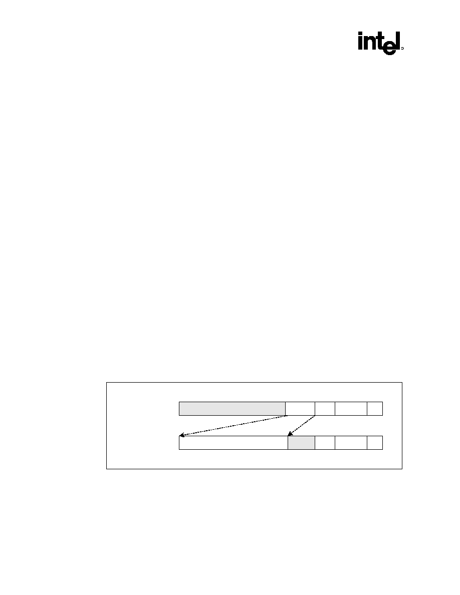
Functional Description
R
116
Intel
ģ
82870P2 P64H2 Datasheet
Type 0 Accesses to the Intel
ģ
P64H2
The configuration space of the bridge in the P64H2 is accessed by a Type 0 configuration
transaction on the hub interface. The bridge configuration space (as well as the I/OxAPIC and hot
plug configuration spaces) cannot be accessed from PCI. The P64H2 responds to a Type 0
configuration transaction when the following conditions are met by the hub interface address:
∑
The bus command is a configuration read or configuration write transaction
∑
Low 2 address bits AD[1:0] must be 00b
∑
The device number matches one of the P64H2 devices (31≠27)
Type 1 to Type 0 Translation
The P64H2 performs a Type 1 to Type 0 translation when the Type 1 transaction is generated on
the hub interface and is intended for a device attached directly to the secondary bus. The P64H2
must convert the configuration command to a Type 0 format so that the secondary bus device can
respond to it. This translation is done only for cycles that originate on the hub interface and target
PCI.
The P64H2 translates a Type 1 configuration transaction into a Type 0 transaction under the
following conditions:
∑
The bus command is a Configuration read or write transaction.
∑
The low 2 address bits on PxAD [1:0] are 01b.
∑
The bus number in address field PxAD [23:16] is equal to the value in the secondary bus
number register in P64H2 configuration space.
The resulting Type 0 address to be driven on PCI is shown in Figure 2 Device numbers are
decoded to generate a single 1 in address bits [31:16]. If the device number is greater than 16, all
bits are 0.
Figure 2. Type 1 to Type 0 Translation
Reserved '0'
Dev ID
O nly one '1'
Fnc
Fnc
0000
Register
Register
01
00
31
15
2
7
10
11
16
1 0
HI Address
PCI Address
Translation_type1-type0
6

Functional Description
R
Intel
ģ
82870P2 P64H2 Datasheet 117
Type 1 to Type 1 Forwarding
The P64H2 forwards a type 1-configuration cycle unchanged to the PCI bus under the following
conditions.
∑
The bus command is a configuration read or write transaction
∑
The low 2 address bits are equal to 01b
∑
The bus number falls in the range defined by the lower limit (exclusive) in the secondary bus
number register and the upper limit (inclusive) in the subordinate bus number register
Type 1 to type 1 forwarding is only done for cycles from the hub interface to PCI.
Type 1 to Special Cycle Forwarding
The P64H2 translates a type 1 configuration write transaction on the hub interface into a special
cycle on PCI, but does not translate a type 1 configuration access on PCI to a special cycle on the
hub interface. A cycle to be translated has the following attributes in the address:
∑
The low 2 address bits on PxAD[1:0]are equal to 01b
∑
The device number in address bits PxAD[15:11] is equal to 11111b
∑
The function number in address bits PxAD[10:8] is equal to 111b
∑
The register number in address bits PxAD[7:2] is equal to 000000b
∑
The bus number is equal to the value in the secondary bus number register in configuration
space
∑
The bus command is a Configuration Write command
The address and data are forwarded unchanged. Devices ignore the address and decode only the
bus command. The data phase contains the special cycle message. The transaction will master
abort, but results in a normal completion on the opposite bus (normal completion status on the hub
interface TRDY# on PCI). If more than one data transfer is requested, the P64H2 responds with a
target disconnect operation during the first data phase.

Functional Description
R
118
Intel
ģ
82870P2 P64H2 Datasheet
4.1.7 Transaction
Termination
Normal Master Termination
As a PCI master, the P64H2 uses normal termination if PxDEVSEL# is returned by the target
within five clock cycles of PxFRAME# assertion. It terminates a transaction when the following
conditions are met:
∑
All write data for the transaction is transferred from the P64H2 data buffers to the target.
∑
The master latency timer expires and the P64H2's bus grant is de-asserted.
Master Abort Termination
If a P64H2-initiated transaction is not responded to with
Px
DEVSEL# within five clocks of
Px
FRAME# assertion, the P64H2 terminates the transaction with a master abort. The P64H2 sets
the received master abort bit in the status register corresponding to the target bus.
Note: When the P64H2 performs a Type 1 to special cycle translation, a master abort is the expected
termination for the special cycle on the target bus. In this case, the
master
abort received bit is not
set, and the Type 1 con-figuration transaction is disconnected after the first data phase.
Target Termination Received by the Intel
ģ
P64H2
When the P64H2 receives a retry or disconnect response from a target, it will re-initiate the
transfer with the remaining length. If the P64H2 receives a target abort, and the cycle requires
completion on the hub interface, the P64H2 will return the target abort code to the hub interface as
the completion status.
Target Termination Initiated by the Intel
ģ
P64H2
The P64H2 returns a target retry to an initiator for memory read transactions when any of the
following conditions is met:
∑
A new transaction for delayed transaction queue.
∑
The request has already been queued, but has not completed on the hub interface.
∑
The delayed transaction queue is full, and the transaction cannot be queued.
∑
A LOCK transaction has been established from the hub interface to PCI.
The P64H2 disconnects an initiator when one of the following conditions is met:
∑
The P64H2 cannot accept any more write data
∑
The P64H2 has no more read data to deliver
∑
If the memory address is non-linear
The P64H2 returns a target abort to PCI when the cycle master aborted or target aborted on the
hub interface.

Functional Description
R
Intel
ģ
82870P2 P64H2 Datasheet 119
4.1.8 Lock
Cycles
A lock is established when a memory read from the hub interface that targets PCI with the lock bit
set, and at least one byte enable active, is responded to with a PxTRDY# by a PCI target. The
P64H2 does not support a split-lock request when no byte enables are asserted on the initial locked
read request. The bus is unlocked when the Unlock Special Cycle is sent on the hub interface.
When the bus is locked, if a memory cycle originates on PCI that is outside the range of the
memory windows, the cycle is retried. No I/O cycles that are destined across the bridge are
accepted, whether the bus is locked or not, and will master abort.
Once the bus is locked, any hub interface cycle to PCI will be driven with the PxLOCK# pin, even
if that particular cycle is not locked. This should not occur; this is because under lock, peer-to-peer
accesses should be blocked.
When one PCI bus segment is locked, the other is still free to accept cycles (i.e., that bus is not
locked). However, these cycles must not be allowed to proceed on the hub interface or the locked
PCI segment. Therefore, once the PCI bus is locked, no more cycles must proceed onto the hub
interface from the non-locked PCI segment, or from the I/OxAPICs.
4.1.9 Error
Handling
The P64H2 checks and generates ECC or parity on the hub interface and parity on the PCI
interfaces. Parity errors must always be reported to some system level software, typically the
device driver or the OS. This section describes how a standard PCI bridge handles these errors.
For enhanced error detection, see Section 4.9.
To support error reporting on the PCI bus, the P64H2 implements the following:
∑
PxPERR# and PxSERR# signals on PCI
∑
DO_SERR special cycle on the hub interface
∑
Primary Device Status Register (PD_STS Register, offset 06≠07h) and Secondary Status
Register (SECSTS Register, offset 1E≠1Fh)
The P64H2 does not have the PERR# or SERR# pins on the hub interface. Further, the P64H2 is
not capable of generating NMI, SMI, or INTR. If enabled, the P64H2 reports the error using the
hub interface DO_SERR special cycle. The device receiving this cycle must forward that cycle to
a device that can generate the error condition (NMI, SMI, SCI) to the processor.

Functional Description
R
120
Intel
ģ
82870P2 P64H2 Datasheet
4.1.9.1
Address Parity Errors
The P64H2 checks address parity for all transactions on both the hub interface and PCI buses, for
all address and all bus commands. Address parity errors are very serious and may abort further
data transfers, depending on the direction of the transfer and the setting of the Parity Error
Response bit (PD_STS Register).
When the P64H2 detects a parity error or multiple-bit ECC error in the header section of a hub
interface packet, it:
∑
Sets the Detected Parity Error bit (bit 15) in the PD_STS Register (offset 06≠07h) if the
address is targeting the device. The bridge devices will log address parity errors independent
of the target address.
∑
Initiates the DO_SERR special cycle, and sets the signaled system error bit (bit 14) in the
PD_STS Register (offset 06≠07h), if the Parity Error Response bit (bit 6) in the PCI Device
Command Register (PD_CMD, offset 04≠05h) is set and SERR# is enabled.
∑
Will attempt to interpret the cycle as best as it can and will forward it with an address parity
error tag to the internal logic where it will abort internally. If a device is not enabled to
respond to parity errors, it will ignore the address parity error (except for setting the Detected
Parity Error bit) and if the address targets that device, accept the cycle and respond as if there
was no address parity error. The cycle will be forwarded to PCI with good address parity if
the cycle targets a bridge and it is not enabled to respond to parity errors.
If a single bit ECC error is detected during the header section, it is corrected and none of the above
occurs.
When the P64H2 detects an address parity error on the PCI interface, the following events occur:
∑
The P64H2 sets the detected parity error bit (bit 15) in the Secondary Status Register
(offset 1E≠1Fh).
∑
If the parity error response bit (bit 0) is 0 in the Bridge Control Register (offset 3E≠3Fh), the
address parity errors are ignored. The cycles would be treated as if no error was observed.
∑
If the parity error response bit is set and the address parity error is observed on memory
cycles, then the cycle is accepted as if the address was correct; Delayed Transactions
established for memory reads and data posted for memory writes. The cycles are forwarded to
the hub interface with correct address parity.
The P64H2 initiates the DO_SERR special cycle on the hub interface and sets the signaled system
error bit in the PCI Primary Device Status (PD_STS) Register, if all of the following conditions
are met:
∑
The SERR# enable bit is set in the PCI Primary Device Command Register.
∑
The parity error response bit is set in the Bridge Control Register.
∑
The SERR# enable bit is set in the Bridge Control Register.

Functional Description
R
Intel
ģ
82870P2 P64H2 Datasheet 121
4.1.9.2
Data Parity Errors
Unlike address parity errors, data parity errors are not considered as severe and transactions are
not aborted. The following sections describe the sequence of events when a data parity error is
detected for the following transactions:
∑
Configuration Write Transactions
∑
Read Transactions (inbound and outbound)
∑
Posted Write Transaction
4.1.9.3
Hub Interface Configuration Write Transactions
When the P64H2 detects a data parity error during a Type 0 configuration write transaction to one
of the P64H2 configuration spaces, the P64H2:
∑
Does not write the data to the configuration register if parity error response is enabled.
∑
Sets the Detected Parity Error bit (bit 15) in the PD_STS Register (offset 06≠07h) of the
target (APIC, hot plug, bridge).
∑
Initiates the DO_SERR special cycle and sets the signaled system error bit (bit 14) in the
PD_STS Register, if the Parity Error Response Enable bit (bit 6) in the PD_CMD Register
(offset 04≠05h) is set.
4.1.9.4
Read Transactions from Hub Interface Targeting PCI
When the P64H2 detects a read data parity error on the PCI bus from a hub interface initiated
read, it:
∑
Sets the Detected Parity Error bit (bit 15) in the Secondary Status Register (offset 1E≠1Fh).
∑
Sets the Data Parity Detected bit (bit 8) in the Secondary Status Register (offset 1E≠1Fh), if
the secondary interface parity error response bit (bit 0) is set in the Bridge Control Register
(offset 3E≠3Fh).
∑
Forces bad parity or a multi-bit ECC error with the data back to the initiator on the hub
interface.
4.1.9.5
Read Transactions from PCI Targeting Hub Interface
When the P64H2 detects a data parity or multi-bit ECC error on a hub interface completion packet
from a previous memory read request on PCI, the P64H2:
∑
Sets the Detected Parity Error bit (bit 15) in the PD_STS Register (offset 06≠07h).
∑
Sets the Data Parity Detected bit (bit 8) in the PD_STS Register (offset 06≠07h) and generates
the DO_SERR special cycle, if the Primary Interface Parity Error Response bit (bit 6) is set in
the PD_CMD Register (offset 04≠05h).
∑
Forwards the bad parity with the data back to PCI.
If a single bit ECC error is detected, it is corrected and none of the above occurs.

Functional Description
R
122
Intel
ģ
82870P2 P64H2 Datasheet
4.1.9.6
Write Transactions on Hub Interface (Intel
ģ
P64H2 As Hub Interface
Target)
When the P64H2 detects a data parity or multi-bit ECC error on a hub interface write request, it:
∑
Sets the Data Parity Error Detected bit (bit 15) in the PD_STS Register
(offset 06≠07h) of the target interface (APIC, hot plug, PCI bridge primary).
∑
If decoded by the bridge, it forwards the bad parity with the data to PCI. If the cycle is
decoded by the APIC or the hot plug controller, (memory writes only), does not perform the
write.
∑
Initiates the DO_SERR special cycle and sets the Signaled System Error bit (bit 14) in the
PD_STS Register, if the Parity Error Response bit (bit 6) is set in the PD_CMD Register.
If a single bit ECC error is detected, it is corrected and none of the above occurs.
4.1.9.7
Write Transactions on Hub Interface (Intel
ģ
P64H2 As Hub Interface
Master)
There is no way of detecting that the MCH detected a parity error from a hub interface posted
write from PCI. Therefore, no action is taken by the P64H2.
4.1.9.8
Write Transactions on PCI (Intel
ģ
P64H2 As PCI Target)
When the P64H2 detects a data parity error on a PCI write, it:
∑
Asserts PERR# two cycles after the data transfer, if the secondary interface parity error
response bit is set in the Bridge Control Register.
∑
Sets the secondary interface Parity Error Detected bit in the Secondary Status Register.
∑
Forces bad parity or a multi-bit ECC error condition to the primary bus.
4.1.9.9
Write Transactions on PCI (Intel
ģ
P64H2 As PCI Master)
When a data parity error is reported on the PCI bus from a hub interface or PCI peer initiated write
request by the target's assertion of PERR#, the P64H2:
∑
Sets the Detected Parity Detected bit (bit 8) in the Secondary Status Register (offset 1E≠1Fh),
if the secondary interface parity error response bit is set in the bridge control register.
∑
Initiates DO_SERR special cycle and sets the Signaled System Error bit in the PD_STS
Register, if all of the following conditions are met:
∑
The SERR# enable bit is set in the PD_CMD Register.
∑
The Secondary Interface Parity Error Response bit is set in the Bridge Control Register.
∑
The Primary Interface Parity Error Response bit is set in the PD_CMD Register.
∑
The P64H2 did not detect the parity error on the hub interface (i.e., the parity error was not
forwarded from the hub interface).

Functional Description
R
Intel
ģ
82870P2 P64H2 Datasheet 123
4.1.9.10 System
Errors
4.1.9.11
PCI SERR# Pin Assertion
When PxSERR# is sampled asserted, the P64H2 sets the received system error bit in the secondary
status register. It generates the DO_SERR special cycle if:
∑
The SERR# Forward Enable bit is set in the Bridge Control Register, and
∑
The Primary SERR# Enable bit is set in the PD_CMD Register.
4.1.9.12
Other System Errors
The P64H2 also conditionally initiates the DO_SERR special cycle for any of the following
reasons:
∑
Parity error reported on target bus during write transactions
∑
Master timeout on delayed transaction if the Primary SERR# Enable bit is set and SERR# due
to Timeout Enable bit (bit 11 of offset 3E≠3Fh) is set.
∑
The MAM bit (Master Abort Mode) is set in the Bridge Control Register and a posted write
from the hub interface results in a master abort on PCI, or a posted write from one PCI
interface results in a master abort on the other PCI interface. (No indication is given back on
the hub interface if a posted PCI write fails on the hub interface ≠ the MCH must handle this
condition).

Functional Description
R
124
Intel
ģ
82870P2 P64H2 Datasheet
4.2 PCI-X
Interface
Both of the P64H2 PCI interfaces support PCI-X. This section does not describe the PCI-X
protocol. Rather, it describes the P64H2 behavior in areas of the specification that are open to
interpretation. For a detailed description, refer to the PCI-X Addendum to the PCI Local Bus
Specification, Revision 1.0.
Unless otherwise noted in this section, the P64H2 follows all rules of the PCI-X Addendum to the
PCI Local Bus Specification, Revision 1.0.
4.2.1 Command
Encoding
Table 23 lists the PCI-X commands supported by the P64H2.
Table 23. Command Encoding
Intel P64H2 As
Intel P64H2 As
Type of Transaction
Master Target
Type of Transaction
Master Target
0000
Interrupt
acknowledge
No No
1000
Alias to Memory
Read Block
No Yes
0001 Special
cycle
No
No
1001
Alias to Memory
Write Block
No Yes
0010 I/O
read
Yes
No
1010
Configuration
Read
Yes No
0011 I/O
write
Yes
No
1011
Configuration
Write
Yes No
0100 Reserved
No
No
1100 Split
Completion
Yes
Yes
0101 Reserved
No
No
1101
Dual Address
Cycle
Yes Yes
0110
Memory Read
DWord
Yes Yes 1110
Memory Read
Block
Yes Yes
0111 Memory
Write
Yes
Yes
1111
Memory Write
Block
No Yes
Functional Description
R
Intel
ģ
82870P2 P64H2 Datasheet 125
4.2.2 Attributes
Table 24 describes how the P64H2 fills in attribute fields where the PCI-X Addendum to the PCI
Local Bus Specification, Revision 1.0 leaves some implementation leeway.
Table 24. Intelģ P64H2 Implementation of Requester Attribute Fields
Attribute Function
No Snoop (NS)
As a target, this bit is forwarded with the transaction to allow the MCH to not snoop the
transaction. It goes to bit 1 in the TD Attribute field of the hub interface packet. It is not
generated by the Intelģ P64H2 as a master from a hub interface packet. The P64H2
takes no action on this bit.
Relaxed
Ordering (RO)
This bit allows relaxed ordering of transactions, which the P64H2 does not permit. This
bit is forwarded in the P64H2 and is never generated on PCI-X from a hub interface
packet.
Tag
Since the P64H2 only has one outstanding request on PCI-X at a time, this field is
always set to 0.
Byte Counts
From the hub interface, this is based upon the length field from the hub interface, which
is DWord based.
4.2.3 Burst
Transactions
The PCI-X Addendum to the PCI Local Bus Specification, Revision 1.0 allows burst transactions
to cross page (in the P64H2's case, this is 4 KB) and 4 GB address boundaries. As a PCI-X
master, the P64H2 will always end the transaction at a 4 KB boundary. As a PCI-X target, the
P64H2 will allow a burst past a 4 KB page boundary.
The P64H2 never issues an immediate response as a target for a burst read command, but it must
be ready with 128 bytes of data space (an ADQ) as an initiator. If it does not have this space
available, it does not issue the transaction.
4.2.4
Device Select Timing
PCI-X targets are required to claim transactions by asserting PxDEVSEL# as shown in Table 25.
The P64H2 always responds as a type A target.
Table 25. DEVSEL# Timing
Decode Speed
PCI-X
1 clock after address phase(s)
Not Supported
2 clocks after address phase(s)
Decode A
3 clocks after address phase(s)
Decode B
4 clocks after address phase(s)
Decode C
5 clocks after address phase(s)
N/A
6 clocks after address phase(s)
Subtractive
Functional Description
R
126
Intel
ģ
82870P2 P64H2 Datasheet
4.2.5 Wait
States
The P64H2 never generates wait states as a target; it ends the transfer.
4.2.6 Split
Transactions
4.2.6.1 Completer
Attributes
Table 26. Intel
ģ
P64H2 Implementation Completion Attribute Fields
Attribute Function
Byte Count Modified (BCM)
This bit is used for diagnostic purposes. The Intelģ P64H2 never
sets this bit.
Split Completion Error (SCE)
The P64H2 only sets this bit if a memory read command from PCI-
X master or target aborted on the hub interface.
Split Completion Message (SCM)
This bit shadows the SCE bit.
4.2.6.2
Requirements for Accepting Split Completions
The P64H2 asserts PxDEVSEL# and discards the data if the Requester ID matches the bridge, but
the tag does not match that of any outstanding requests from this device, or if the byte count
exceeds that of the split request.
The hub interface accepts more than one completion required request from the hub interface, but
only one will be pending on any PCI/PCI-X interface at a time.
4.2.6.3
Split Completion Messages
The P64H2 can only generate error messages for cycles that cross the bridge that master or target
abort. No DWord cycles will cross the bridge that requires completion (i.e., I/O cycles). Therefore,
the P64H2 can only generate a "PCI-X Bridge Error" completion message for the memory read
commands as indicated in Table 27.
Table 27. Split Completion Abort Registers
Index Message
00h
Master-Abort: The Intelģ P64H2 encountered a Master-Abort on the destination bus.
01h
Target-Abort: The P64H2 encountered a Target-Abort on the destination bus.

Functional Description
R
Intel
ģ
82870P2 P64H2 Datasheet 127
4.2.7
Arbitration Among Multiple Split Completions
The P64H2 will fairly arbitrate amongst all active split completions such that each completion will
get a fair shot at running on PCI. If there are multiple completions waiting to use PCI, the P64H2
will internally arbitrate based upon its MLT value, even if no other agents are requesting on the
bus. Therefore, the P64H2 will end one transaction when its MLT expires, reload, and start
another transaction.
If any particular transaction runs out of data and there are other active transactions to run, the
P64H2 will also switch to the next agent, even if the MLT has not expired for that transaction.
Finally, the prefetch algorithm will be altered such that several transactions can be active at one
time. See Section 3.2.48 for more information on prefetch algorithms.
4.2.8
Transaction Termination as a PCI-X Target
Retry
The P64H2 will retry a cycle when the Split Request queue is full. (i.e. we already have 4 current
and 4 pending Split Transactions). It will always have room to accept a split completion as it has a
dedicated buffer for split completions. It will also retry a cycle when the bus is locked. The P64H2
stores no state from the transaction on a retry.
Split Response
All cycles that cross the bridge receive a split response termination, if they are not retried.
Master-Abort
Any I/O transaction that would cross from PCI-X to either the hub interface or the peer bridge are
not decoded and result in a master abort to the PCI-X initiator.
4.2.9 Arbitration
The P64H2 always parks on the last agent to use PCI. This allows PCI devices operating as a
single stream to stay on the PCI bus for the duration of their transfer.

Functional Description
R
128
Intel
ģ
82870P2 P64H2 Datasheet
4.2.10 System
Initialization
Encoding on the PxM66EN and PxPCIXCAP pin as shown below identifies the capabilities of the
system. The following tables are included from the PCI-X Addendum to the PCI Local Bus
Specification, Revision 1.0 for easy reference.
Table 28. M66EN and PCIXCAP Encoding
PxM66EN
PxPCIXCAP
PCI Capability
PCI-X Capability
Ground
Ground
33 MHz
Not capable
Not connected
Ground
66 MHz
Not capable
Ground
Pull-down
33 MHz
PCI-X 66 MHz
Not connected
Pull-down
66 MHz
PCI-X 66 MHz
Ground
Not connected
33 MHz
PCI-X 133 MHz
Not connected
Not connected
66 MHz
PCI-X 133 MHz
Table 29. PCI-X Initialization Pattern
Clock Period
(ns)
Clock Freq
(MHz)
PxDEVSEL# PxSTOP# PxTRDY# Mode
Max Min Min Max
PCI 33
30
0 33
Deasserted Deasserted Deasserted
PCI 66
30
15
33 66
Deasserted
Deasserted Asserted PCI-X 20 15 50 66
Deasserted Asserted Deasserted
PCI-X 15 10 66 100
Deasserted Asserted Asserted PCI-X 10 7.5 100
133
Asserted Deasserted
Deasserted
PCI-X
Asserted Deasserted Asserted PCI-X
Asserted Asserted
Deasserted
PCI-X
Asserted Asserted Asserted
PCI-X
Reserved

Functional Description
R
Intel
ģ
82870P2 P64H2 Datasheet 129
4.2.11 Bridge
Buffer
Requirements
The P64H2 always has 128 bytes (1 ADQ) available for accepting memory write, split completion,
and immediate read data. The P64H2 contains 1.5 KB of data total for inbound transactions.
The P64H2 PCI-X interface terminates all memory transactions (Memory Read DWord, Memory
Read Block, and Alias to Memory Read Block) that address the MCH with a Split Response.
Other split transaction commands are not decoded by the P64H2.
The P64H2 does not implement any split completion buffer allocation algorithm as listed in the
PCI-X Addendum to the PCI Local Bus Specification, Revision 1.0. This is not necessary. The
P64H2 never requests, on the hub interface, more than it has buffer space for on returns, and does
not initiate a cycle from the hub interface that it cannot accept as a return. The bridge rules of the
specification already allow the PCI-X interface to retry split completions if the bridge is
temporarily full.
Therefore, the split transaction control registers are not used by the P64H2.
4.2.12
Cycle Translation Between Interfaces
4.2.12.1
Conventional PCI to PCI-X / Hub Interface
Table 30. Conventional PCI to PCI-X / Hub Interface
Conventional PCI Command
PCI-X as Target
Hub Interface as Target
I/O Read / Write
Master Abort at source (not supported)
Configuration Read / Write
Master Abort at source (not supported)
Memory Read, Memory read line,
memory read multiple
Forward to hub interface unless
the peer mode test bit is set
Memory Read
Memory Write
Memory Write
Memory Write
Memory Write and Invalidate
Memory Write
Memory Write
The attribute phase on the PCI-X transfer has the following characteristics:
∑
The P64H2 uses the primary bus number as its Bus Number
∑
Sets the Device Number and Function Number fields to 0
∑
Clears the Relaxed Order or No Snoop attribute bits on transactions forwarded from a
conventional bus.

Functional Description
R
130
Intel
ģ
82870P2 P64H2 Datasheet
4.2.12.2
PCI-X to Conventional PCI (peer) / Hub Interface
Table 31. PCI-X to Conventional PCI (peer) / Hub Interface
PCI-X Command
PCI as Target
Hub Interface as Target
I/O Read / Write
Master Abort at source (not supported)
Configuration Read / Write
Master Abort at source (not supported)
Memory Read DWord, Memory
Read Block
Forward to hub interface unless
the peer mode test bit is set
Memory Read
Memory Write, Memory Write Block
Memory Write
Memory Write
4.2.13 Locked
Transactions
The P64H2 is not locked until the target has completed at least the first data phase as an
Immediate Transaction or a Split Transaction (target signals Split Response).
4.2.14 Error
Support
General
As a PCI-X target, the P64H2 bridge responds as specified in the PCI-X Addendum to the PCI
Local Bus Specification, Revision 1.0, except that all memory read transactions that leave this
bridge and target the other bridge will be set to the hub interface, unless the peer mode test bit is
set.
Special Parity Error Rule for Split Response
If the P64H2 calculates a data parity error when a target signals Split Response for a read
transaction, it records the error as described in Section 5.4.1 of the PCI-X Addendum to the PCI
Local Bus Specification, Revision 1.0. Furthermore, if the P64H2 is enabled to assert PERR# on
the secondary bus and enabled to assert SERR# on the hub interface, it must generate a DO_SERR
packet on the hub interface.
4.2.15
Transaction Termination Translation Between Interfaces
Though the P64H2's primary bus is the hub interface, from a register and software perspective, the
hub interface is a PCI-X bus and the P64H2 is a PCI-X bridge that supports a secondary bus
configured as either PCI or PCI-X.
The PCI-X Addendum to the PCI Local Bus Specification, Revision 1.0 (Section 8.7.1.5) modified
the behavior of a bridge from that specified in the PCI-to-PCI Bridge Architecture Specification,
Revision 1.1 regarding returning completions on the primary bus when the secondary bus
transaction terminates in either a master abort or target abort. In general, the PCI-X Addendum to
the PCI Local Bus Specification, Revision 1.0 does not honor the Master Abort Mode bit for
cycles requiring completions and returns to the primary bus the termination that occurred on the
secondary bus without any translation.

Functional Description
R
Intel
ģ
82870P2 P64H2 Datasheet 131
The following sections describe the behavior of the P64H2 on both the hub interface and PCI/PCI-
X Bus under various termination conditions. For specific information as to why the P64H2's PCI,
PCI-X, or hub interface generates a specific termination, see the specific sections on the interface
above.
4.2.15.1
Behavior of Hub Interface Initiated Cycles to PCI/PCI-X Receiving
Immediate Terminations
The behavior described for completion required cycles is independent of the setting of the Master
Abort Mode bit and is independent of whether the cycle is exclusive (locked) or not. The P64H2
will return all 1s on data bytes for a read completion that terminates in either Master Abort or
Target Abort.
Table 32. Immediate Terminations of Completion Required Cycles to PCI/PCI-X
PCI/PCI-X
Termination
Hub Interface Completion
Status Register Bits Set
Successful
Successful
Mater Data Parity Error (Sec)
1
Mater Abort
Master Abort
Received Mater Abort (Sec)
Target Abort
Target Abort
Received Target Abort (Sec)
Signaled Target Abort (Pri)
Master Data Parity Error (Sec)
1
NOTES:
1. The Master Data Parity Error bit is set only if a data parity error was encountered on the PCI/PCI-X Bus.
Table 33. Immediate Terminations of Posted Write Cycles to PCI/PCI-X
PCI/PCI-X
Termination
MAM Bit
Hub Interface
Cycle
Status Register Bits Set
Successful N/A None
None
Master Abort
1
Do_SERR
1
Received Master Abort (Sec)
Signaled System Error (Pri)
1
Master Abort
0
None
Received Master Abort (Sec)
Target Abort
N/A
DO_SERR
1
Received Target Abort (Sec)
Signaled System Error (Pri)
1
NOTES:
1. The DO_SERR cycle and setting of the Signaled System Error bit only occur if the SERR#
enabled in the Primary Command Register is set.

Functional Description
R
132
Intel
ģ
82870P2 P64H2 Datasheet
4.2.15.2
Behavior of Hub Interface Initiated Cycles to PCI-X Receiving Split
Terminations
The behavior described in the following table is independent of the Master Abort Mode bit and
whether or not the cycle is exclusive (locked) or not. P64H2 will return all 1s on all data bytes for
a read completion that terminates in either Master Abort or Target Abort on the hub interface.
Note that when a target or master abort is returned on the hub interface, the attached PCI/PCI-X
bus is not locked. This is of special importance to the completion messages of data parity error,
byte count out of range, write data parity error, device specific, and reserved / illegal codes.
P64H2 must not lock its bus on these errors, even though they are not explicitly master or target
aborts on the PCI-X interface.
Table 34. Split Terminations of Completion Required Cycles to PCI-X
Message
PCI-X Split
Termination
Class Index
Hub Interface
Completion
Status Register Bits Sets
Successful 0
00h
Successful
∑
Master Data Parity Error (Sec), if
encountered
Master Abort
1
00h
Master Abort
∑
Received Master Abort (Sec)
Target Abort
1
01h
Target Abort
∑
Received Target Abort (Sec)
∑
Signaled Target Abort (Pri)
Write Data Parity Error
1
02h
Target Abort
∑
Master Data Parity Error (Sec)
∑
Signaled Target Abort (Pri)
Byte Count Out of Range
2
00h
Target Abort
∑
Signaled Target Abort (Pri)
Write Data Parity Error
2
01h
Target Abort
∑
Master Data Parity Error (Sec)
∑
Signaled Target Abort (Pri)
Device Specific
2
8Xh
Target Abort
∑
Signaled Target Abort (Pri)
Reserved/Illegal Others
Target
Abort
∑
Signaled Target Abort (Pri)

Functional Description
R
Intel
ģ
82870P2 P64H2 Datasheet 133
4.2.15.3
Hub Interface Action on Immediate Responses to PCI-X Split
Completions
Table 35 indicates what the P64H2 will do if it is returning a split completion to PCI-X from a
normal hub interface completion and receives an immediate response indicating an error. Table 36
indicates the behavior of PCI/PCI-X Initiated Cycles to Hub Interface.
Table 35. Response to PCI-X Split Completions
Split Completion
Termination
Hub Interface Cycle
Status Register Bits
Successful None
∑
None
Master Abort
DO_SERR
1
∑
Received Master Abort (Sec)
∑
Split Completion Discarded (Sec)
∑
Signaled System Error (Pri)
1
Target Abort
DO_SERR
1
∑
Received Target Abort (Sec)
∑
Split Completion Discarded (Sec)
∑
Signaled System Error (Pri)
1
NOTES:
1. The DO_SERR cycle and setting of the Signaled System Error bit only occur if the SERR# enabled in
the Primary Command Register is set.
Table 36. Terminations of Completion Requited Cycles to Hub Interface
Hub Interface Termination
PCI Completion
Status Register Bits Set
Successful
Successful
∑
None
Master Abort (PCI)
Target Abort
1
∑
Received Master Abort (Pri)
∑
Signaled Target Abort (Sec)
Master Abort (PCI-X)
Split Master Abort
2
∑
Received Master Abort (Pri)
Target Abort
Target Abort (PCI)
1
Split Target Abort (PCI-X)
2
∑
Received Target Abort (Pri)
∑
Signaled Target Abort (Sec)
Master and Target Abort
Target Abort (PCI)
1
Split Target Abort (PCI-X)
2
∑
Received Master Abort (Pri)
∑
Received Target Abort (Pri)
∑
Signaled Target Abort (Sec)
NOTES:
1. The P64H2 will only signal Target Abort if the error has been logged from the hub interface before the
initial connect by PCI or when the PCI master reconnects after a previous disconnect. If the P64H2
receives an abort on the hub interface in the middle of a read completion stream, it will not interrupt the
stream to signal Target Abort.
2. The P64H2 will issue a Split Completion Error Message with either Master Abort or Target Abort for the
remaining completion sequence if an abort is detected on the hub interface. If several bytes of data are
returned successfully from the hub interface and have not yet been sent back on PCI-X, when the abort

Functional Description
R
134
Intel
ģ
82870P2 P64H2 Datasheet
is detected on the hub interface, the P64H2 will stop the current sequence for that data (if it was
running) and generate the Split Completion Error Message.
4.2.16 Configuration
Transactions
Type 0 configuration transactions are issued when the intended target resides on the same PCI-X
bus as the initiator. A Type 0 configuration transaction is identified by the configuration command
and the lowest 2 bits of the address set to 00b.
Type 1-configuration transactions are issued when the intended target resides on another PCI-X
bus, or when a special cycle is to be generated on another PCI-X bus. A Type 1 configuration
command is identified by the configuration command and the lowest 2 address bits set to 01b.
The register number is found in both Type 0 and Type 1 formats and gives the DWord address of
the configuration register to be accessed. The function number is also included in both Type 0 and
Type 1 formats and indicates which function of a multifunction device is to be accessed. For
single-function devices, this value is not decoded. Type 1 configuration transaction addresses also
include a 5-bit field designating the device number that identifies the device on the target PCI-X
bus that is to be accessed. In addition, the bus number in Type 1 transactions specifies the PCI-X
bus to which the transaction is targeted.

Functional Description
R
Intel
ģ
82870P2 P64H2 Datasheet 135
4.3
Hot Plug Controllers
The P64H2 hot plug controller allows PCI card removal, replacement, and addition without
powering down the system. In this section the standard specification signal names are used for the
hot plug signal names and PCI signal names. For actual P64H2 signal names, the letters "A" and
"B" are used in the signal names to distinguish between PCI Interface A and PCI Interface B.
4.3.1 System
Architecture
The P64H2 hot plug controller resides in Function 0 of the secondary bus device 31. It supports
three to six PCI slots through an input/output serial interface when operating in Serial Mode, and 1
to 2 slots through an input/output parallel interface when operating in Parallel Mode. The input
serial interface is polling and is in continuous operation. The output serial interface is "demand"
and acts only when requested. These serial interfaces run at about 8.25 MHz regardless of the
speed of the PCI bus. In parallel mode, the P64H2 performs the serial to parallel conversion
internally, so the serial interface cannot be observed. However, internally the hot plug controller
always operates in a serial mode.
4.3.1.1 Output
Control
The output interface is responsible for driving seven bits per slot (plus 8 general purpose output
bits in serial mode).
∑
POWER ENABLE: Connected to an analog component designed to regulate current and
voltage of the slot, and generates a (power) fault signal when an abnormal condition is
detected.
∑
CLOCK ENABLE#, BUS ENABLE#: Connects the PCI bus and clock signal of the slot to
the system bus PCI bus via FET isolation switches.
∑
RESET#: Connected to the PCIRST# pin of the slot.
∑
AMBER and GREEN LEDs: Connected to LEDs on the chassis to indicate a slot's status to
the user.
∑
General Purpose Outputs: (only in Serial Mode)
The general-purpose output bits are set using bits 0 through 7 of the General Purpose Output
Register (Offset 13h) in memory space. The other output bits are set by the hot plug controller
based on the Slot Power Enable Register (Offset 2Dh) and the Slot Enable Register (Offset 01h) in
memory space.
In a well-behaved environment, the output sequences are initiated by software. However, the hot
plug controller can act without software intervention to disable power to a slot and turn off its
LEDs, if a PCI card is being removed from a powered PCI slot.

Functional Description
R
136
Intel
ģ
82870P2 P64H2 Datasheet
4.3.1.2 Input
Control
The input interface captures eight inputs from each slot:
∑
SLOT SWITCH: Determines whether a slot should be powered. Connected to the slot switch
on the chassis.
∑
FAULT#: Over-current / Under-volt indication: When asserted, the P64H2, if enabled,
immediately asserts reset and disconnects the slot from the bus.
∑
PRSNT1# and PRSNT2#: Signals which determine whether or not a card is installed and to
budget system power. These inputs are connected to the PRSNT1# and PRSNT2# pins on the
PCI card.
∑
M66EN: Determines if a card can be added to the bus without reducing the clock frequency
of the PCI bus.
∑
PCIXCAP1 and PCIXCAP2: Determines if a slot is PCI-X capable, and if so, whether it can
operate at 133 MHz.
∑
1 User-Defined Input: Stored in the Hot plug Non-Interrupt Inputs Register (although
marked as reserved bits 24 through 29.). This is available only in Serial Mode.
4.3.1.3 Stutter
Mode
Stutter mode minimizes the amount of external hardware required to implement fewer than six
slots. The stutter mode used corresponds to the number of slots supported by the system. Stutter
mode selection is determined by HP_SLOT[2:0], as shown in Table 37.
Table 37. Stutter Logic Modes
HP_SLOT[2:0] #
of
Slots
Inputs Outputs
000
Hot Plug Disabled
001 Parallel
Mode--No Stutter
010 Parallel
Mode--No Stutter
011 3
Yes
Yes
100 4
Yes
Yes
101 5
Yes
Yes
110 6
Yes
No
111
Reserved (Hot plug Disabled)
Figure 3 shows how 6-slot stutter mode serial inputs are sampled. The serial clock stutters at bit
positions 6 and 7, but internally the bit shifted last (bit 5 in this example) is sampled as the next
successively stuttered bits (bit 6 and 7 in this example). This is why in some registers (e.g., the
memory register HMIC) bits for disabled slots take their values from the last enabled slot.
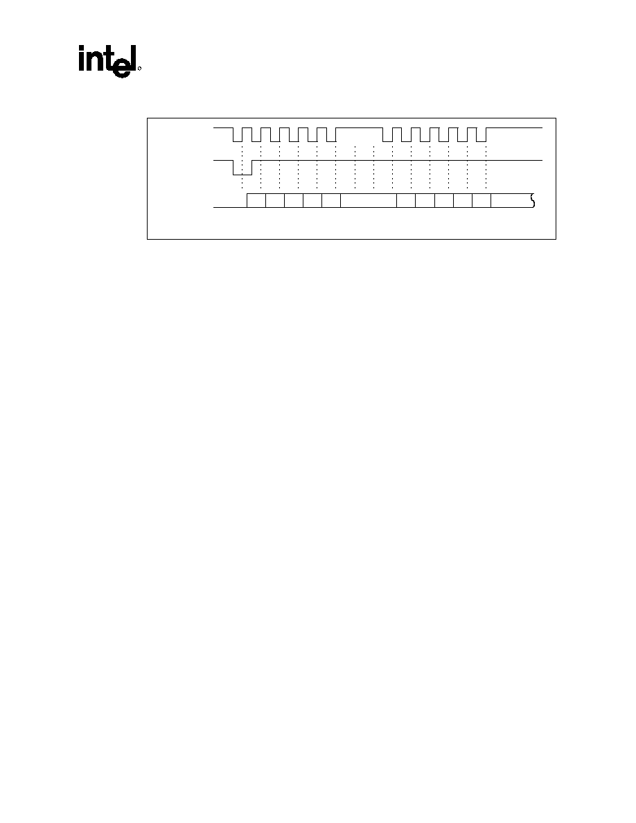
Functional Description
R
Intel
ģ
82870P2 P64H2 Datasheet 137
Figure 3. Serial Input 6-slot Stutter Mode
hotplug_6-slot_stutter
0
1
2
3
4
5
6
7
8
9
10
11
HP_SIC
HP_SIL#
HP_SID
4.3.1.4
Serial Input Stream
The serial input stream constantly runs once the P64H2 is out of reset (RSTIN# deasserted). Under
normal operation, the input stream consists of a repeating series of 8 bytes of serial data. Note,
however, that because of stutter logic, some of these serial input bits are not shifted out of the
external shift registers (see previous section). It is possible to extend the serial input stream length
to 16 bytes through the use of the Serial Input Register.
The first 4-bytes of the serial input stream are interrupting inputs. The remaining 4-bytes are non-
interrupting inputs. Because only six-slots are supported by the P64H2, only 24 of the 32
interrupting inputs are available. Each slot has six inputs. The first group of inputs function as the
slot switches. The second group are slot power fault indicators. The remaining 12 interrupt-
capable inputs are the slot card present bits.
A change on any of the switch inputs initiates a 15 ms glitch filter timer. If a change is detected on
any slot switch input, the switch input is re-scanned 32 times within a 15 ms time interval. If the
switches remain stable for 32 samples, the HMIC is updated to reflect the change in state. If any
switch is still changing state, the glitch filter counter is cleared and the sequence restarts. If not
masked, a switch change interrupt is also generated after the HMIC changes state. The interrupt
function can be masked using the HMIR, but the HMIC always reflects a state change.
A change on any of the non-switch inputs causes an immediate change in the state of the HMIC.
An interrupt is also generated unless masked in the HMIR. After a non-switch input changes state,
further updates to all other non-switch bits of the HMIC is inhibited for an 8 ms de-bounce period.
This prevents a rapid succession of interrupts from being generated before software has time to
react.
In summary, an interrupt is generated and the interrupt pending bit is set in the MCNF Register in
memory space if all of the following are true:
∑
An interrupt is not already pending, and
∑
A switch input changes state and remains in its new state at the end of the glitch filter time
period, or a non-switch interrupting input has changed state at the beginning of the de-bounce
period, and
∑
The interrupt mask bit for that input is cleared (logic 0).
If an interrupt bit changes state in the HMIC and is not masked, the value is frozen in then HMIC
until acknowledged by writing 1 to this bit position. In the case of an unmasked non-switch input
already causing an interrupt to be generated, if the de-bounce timer expires and the interrupt has

Functional Description
R
138
Intel
ģ
82870P2 P64H2 Datasheet
not been serviced (acknowledged), a single change in the state of an input could occur and be
posted (or buffered). The buffered value of this bit cannot be observed until the prior interrupt is
acknowledged.
Non-interrupting inputs follow at bytes 4≠15. The P64H2 continually scans bytes 4≠7 and stores
this data in the Hot plug Non-Interrupt Input Register. The timing of non-interrupt input scanning
for bytes 4≠7 is identical to that of interrupt-capable inputs. Since scan timing cannot be easily
predicted, the memory register bit MCNF[12] status bit allows software to determine when an
eight-byte scan sequence is complete.
The current state of any of the inputs from bytes 0≠15 can also be read one byte at a time through
the Serial Input Byte Pointer and Data Registers. When the byte pointer is written, the P64H2's
next scan in sequence continues shifting data in, until the appropriate byte is latched in the data
port. When the Serial Input Byte Pointer has been written, the Serial Input Busy Status bit
indicates when shifting of the selected input byte is complete. The value read from the data port is
unpredictable if it is read before shifting is complete. Bytes 8≠15 can be accessed only using the
Serial Input Byte Pointer and Data port. Note that bytes 8≠15 are not stuttered during scan in.
The shift clock frequency is a divide by 8 of the hub interface clock used to clock the hot plug
unit, and is approximately 8.25 MHz. External shift registers are loaded when HP_SIL# is
asserted. Shift registers can be loaded either synchronously or asynchronously. They are clocked
on the rising edge of the shift clock (HP_SIC). The serial data input pin (HP_SID) to the P64H2 is
sampled on the succeeding rising edge of the HP_SIC.
Slot Switch
The presence of logic 0 on these pins indicates that the slot is closed and can be powered on. A
logic 1 indicates that the slot should immediately be powered off. The P64H2, if enabled, auto-
powers down any slot whose switch input changes from 0 to 1, if the slot is currently powered on.
The P64H2 also powers off the LEDs for that slot.
Slot Fault
The power fault input is connected to an external device for each slot that provides the following
functions:
∑
Limits in-rush current to the slot so that common power rails supplying power to other slots
and system board devices do not droop or glitch as slot power is switched on.
∑
Detects over-current, under-voltage, and over-voltage conditions on each supply rail.
∑
Immediately removes power from the slot when a fault is detected so that the power supply to
other system components and slots is not adversely affected.
∑
Immediately isolates the slot from the bus and resets the slot so that input protection diodes on
the un-powered card do not present an excessive load on bus signals. This function is
controlled by the P64H2 when operating in one of the Parallel Modes.
∑
Indicates faults to the P64H2 by driving the respective slot fault pin to logic 0.
When P64H2 detects a slot fault, either on the input serial stream, or the parallel mode fault inputs,
the internal power fault latches will latch this event for each slot. The internal power fault latches
will always latch the power fault inputs, regardless of the state of SPFLE in the MCNF Register in

Functional Description
R
Intel
ģ
82870P2 P64H2 Datasheet 139
memory space. If power faults are disabled via the PFE bit in the MCNF Register (memory or PCI
configuration space), the power fault latches will never see power fault events.
The HMIC Register can be programmed to reflect either the slot power fault inputs (parallel or
serial), or the output of the internal power fault latches. This is done by setting/clearing the SPFLE
bit in the MCNF Register in memory space.
The internal power fault latches can be reset by either removing power from the appropriate slot,
or by clearing the PFE bit (this clears all power fault latches).
When running in 1-slot or 2-slot parallel mode, the parallel mode power fault inputs are
immediately latched by the internal power fault latches. The outputs of these latches are then used
to asynchronously disconnect the slot power, bus enable, and clock enable, as well as assert the
slot reset. This "gating logic" remains active as long as the internal power fault latch is active.
These latches can be cleared by software initiating a slot disable cycle, thus disconnecting power
to the slot and thus clearing the power fault latch. A slot disable cycle can also be initiated by
hardware via an auto power down event caused by opening a slot switch.
Downstream cycles targeting a PCI bus segment during a hot plug device's power fault event on
that bus could cause a system hang if the slot is not yet disabled by the hot plug controller. The hot
plug controller should initiate a slot disable cycle (via software or hardware) to disable the slot and
clear the power fault latches before any cycles are allowed to run on the PCI bus.
Note: The power fault latches can be cleared by clearing the PFE bit and this will cause the "gating
logic" to be removed. This will cause the slot power, bus enable, clock enable to all be
asynchronously enabled, and the slot reset asynchronously disabled. This is not desired behavior
and should be avoided.
PRSNT#[2:1]
These pins are provided so that software can detect the presence of a board and keep a tally of the
total amount of power used by hot plug slots. They can generate an interrupt when they change
state.
M66EN
In hot plug systems, M66EN is slot-specific. When HPx_SLOT[2:0] is not 000, the system
initially powers up at 33 MHz, and all hot plug slots are scanned by system software. If the
M66EN bits are all high for the closed slots, then software can reset the system for 66 MHz
operation, and turn on power to the cards.
PCIXCAP1/2
PCIXCAP1 and 2 represent a "serialized" version of the three-state PCIXCAP pin present on each
slot. PCIXCAP1 represents whether the PCIXCAP pin was ground or not ground (i.e., PCI-X
capable), and PCIXCAP2 represents whether the PCIXCAP pin was low (66 MHz only) or high
(133 MHz capable). The system initially powers up at 33 MHz PCI, and all hot plug slots are
scanned. If the system is capable, the bus is reset to run in the appropriate PCI-X mode.

Functional Description
R
140
Intel
ģ
82870P2 P64H2 Datasheet
Input Shift Register Assignments
Three pins control the serial stream: HPSIL#, HPSIC and HPSID. The P64H2 always scans in at
least eight bytes. The assignments are shown in Table 38.
Table 38. Shift Register Data
Bit
Byte 0
Byte 1
Byte 2
Byte 3
0
Slot A switch
(0 = closed)
Slot A fault#
(0 = fault)
Slot A PRSNT2#
Slot A PRSNT1#
1
Slot B switch
Slot B fault#
Slot B PRSNT2#
Slot B PRSNT1#
2
Slot C switch
Slot C fault#
Slot C PRSNT2#
Slot C PRSNT1#
3
Slot D switch
Slot D fault#
Slot D PRSNT2#
Slot D PRSNT1#
4
Slot E switch
Slot E fault#
Slot E PRSNT2#
Slot E PRSNT1#
5
Slot F switch
Slot F fault#
Slot F PRSNT2#
Slot F PRSNT1#
6
Stutter (not used)
Stutter (not used)
Stutter (not used)
Stutter (not used)
7
Stutter (not used)
Stutter (not used)
Stutter (not used)
Stutter (not used)
Bit
Byte 4
Byte 5
Byte 6
Byte 7
0
Slot A M66EN
Slot A PCIXCAP1
Slot A PCIXCAP2
User Defined Input
1
Slot B M66EN
Slot B PCIXCAP1
Slot B PCIXCAP2
User Defined Input
2
Slot C M66EN
Slot C PCIXCAP1
Slot C PCIXCAP2
User Defined Input
3
Slot D M66EN
Slot D PCIXCAP1
Slot D PCIXCAP2
User Defined Input
4
Slot E M66EN
Slot E PCIXCAP1
Slot E PCIXCAP2
User Defined Input
5
Slot F M66EN
Slot F PCIXCAP1
Slot F PCIXCAP2
User Defined Input
6
Stutter (not used)
Stutter (not used)
Stutter (not used)
Stutter (not used)
7
Stutter (not used)
Stutter (not used)
Stutter (not used)
Stutter (not used)
4.3.1.5
Serial Output Stream
Reading and writing the internal serial output control registers does not automatically initiate
output shifting. The shift output process is initiated by writing the SOGO bit in the MCNF
Register in memory space to 1. When this bit is set, it is not reset until the external shift registers
and latches are in their proper state. If the SOGO bit is written to 0 or 1 while the SOGO bit is set,
the write is ignored.
Although blinking of LEDs requires the use of the serial output logic, the operation of the SOGO
bit is unaffected by this. If an update for a blink was already in progress when the SOGO bit was
written, it may increase the amount of time that the SOGO bit remains set. The SOGO bit state
reflects only the state of software-originated shift output events and not those triggered by
hardware. Note that the OOB bit will reflect the state of the on/off state machine which controls
shift out events, regardless of whether they are hardware or software initiated events.

Functional Description
R
Intel
ģ
82870P2 P64H2 Datasheet 141
The on/off state machine executes a shift for any of the following reasons:
∑
The SOGO bit was set by software (even if no slot enable bits have changed state).
∑
A Hot plug slot switch has opened (provided that the respective slot is on).
∑
At least one LED has been programmed to blink and the blink timer has expired.
∑
A PCI configuration space write to byte offset 43h after RSTIN# deassertion. (The system
ROM firmware usually does this early, after or while configuring the MCNF Register in
configuration space).
The LED control outputs are updated with a single pass through the output shift registers. The
PWREN, RESET#, CLKEN#, and BUSEN# bits, however, require multiple passes. The shift
sequence changes depending on which bits have been set or reset in the Slot Enable Register when
the SOGO bit is set:
∑
No Slot Enable bits have changed: The serial outputs are updated in a single pass.
∑
At least one Slot Enable bit has changed from 0 to 1 when SOGO is set: Executes a slot
enable sequence.
∑
At least one Slot Enable bit has changed from 1 to 0: Executes a slot disable sequence.
∑
Some Slot Enable bits have changed from 0 to 1 and some have changed from 1 to 0:
Executes two sequences ≠ first a disable sequence then an enable sequence.
The SOGO bit can be configured to generate an interrupt when it changes from 1 to 0 through the
SOIE bit in the MCNF Register.

Functional Description
R
142
Intel
ģ
82870P2 P64H2 Datasheet
Shift Register Assignments
GPO[7:0] are shifted out before the reset enables. This is done to support a system that does not
need the GPOA outputs. For a system using less than six slots, stutter logic can be utilized to
reduce the number of output shift registers and latches. Serial mode output shifting is shown in
Table 39.
Table 39. Serial Mode Output Shift-Out SR Bit Order
SR Bit
Function
SR Bit
Function
SR Bit
Function
0
gpo7
15
ambled 1
30
busen 5
1
gpo6 16 grnled
2 31 busen
6
2
gpo5
17
ambled 2
32
clken 1
3
gpo4 18 grnled
3 33 clken
2
4
gpo3
19
ambled 3
34
clken 3
5
gpo2 20 grnled
4 35 clken
4
6
gpo1
21
ambled 4
36
clken 5
7
gpo0 22 grnled
5 37 clken
6
8
reset# 1
23
ambled 5
38
pwren 1
9
reset# 2
24
grnled 6
39
pwren 2
10
reset# 3
25
ambled 6
40
pwren 3
11
reset# 4
26
busen 1
41
pwren 4
12
reset# 5
27
busen 2
42
pwren 5
13
Reset# 6
28
busen 3
43
pwren 6
14
grnled 1
29
busen 4
LEDs
Each slot has a green and amber LED for communicating slot status to the user. Each LED has 4
states (ON, OFF, BLINK PHASE A, and BLINK PHASE B) controlled by the LED Control
Register (LEDC).
A single timer controls blinking for all LEDs and is hardwired to 1 Hz at a 50% duty cycle,
derived from the PCI clock frequency. Phase A is on for the first half of each one-second period
and phase B is on for the second half.
When a switch for a slot indicates that the slot has been opened, both LEDs are turned off by the
P64H2. The LEDs can later be programmed by software to turn on or blink the LEDs, whether or
not the slot is open. It is the responsibility of software to insure that the LEDs never indicate that a
slot is powered down when the slot has power.

Functional Description
R
Intel
ģ
82870P2 P64H2 Datasheet 143
GPO
General-purpose outputs are used for non-slot specific system functions. These outputs are part of
the serial output chain but are not affected by the number of slots detected on HP_SLOT[2:0].
4.3.1.6 Power
Sequencing
Each slot uses 4 control signals to enable and disable PCI-X cards: PWREN, CLKEN#, BUSEN#
and RESET#. Power sequencing can be performed in one of two ways, as selected by the CBLE
(Connect Bus Last Enable) bit in the MCNF Register in PCI configuration space. If CBLE is
cleared, the PCI bus is connected before the slot reset is deasserted. If CBLE is set, the PCI bus is
connected after the slot reset has been deasserted.
Any slot can be individually powered on by setting the appropriate bit of the Slot Power Enable
register. These bits affect only the state of the PWREN pin for that slot; they do not affect the
clock, connection to the bus, or slot reset.
Power Up (CBF Mode)
When a slot is to be turned on in CBF mode, the outputs are updated in the following sequence:
2. Assert PWREN, but keep BUSEN# and CLKEN# deasserted and RESET# asserted. Shift the
new pattern to the shift registers.
3. Clock the parallel latch HP_SOL. The new values for LEDs are clocked out at this point as
well.
4. With PWREN asserted, assert CLKEN# bit but leave BUSEN# deasserted and RESET#
asserted. Shift the new pattern to the shift registers.
5. Wait for 500 ms for power to stabilize.
6. Arbitrate for an idle bus, and clock the parallel latch HP_SOL.
7. With PWREN and CLKEN# asserted, assert BUSEN# to connect the bus, and deassert
RESET# Shift the new pattern to the shift registers.
8. Wait for 500 ms for expansion card clocks to stabilize.
9. Arbitrate for an idle bus time, and clock the parallel latch HP_SOL. However, since
HP_SOLR is not clocked, the RESET# pin remains asserted to the device.
10. Wait for 330 ns.
11. Clock the parallel latch HP_SOLR, to negate reset.
Table 40. Power Up Timings (CBF Mode)
Timing Event
Minimum
1
Maximum Units
PWREN Assertion to CLKEN# Assertion
500
505
ms
CLKEN# Assertion to BUSEN# Assertion
500
505
ms
BUSEN# Assertion to RESET# Deassertion
330
330
ns
NOTES:
1. Arbitration latency affects the minimum time.
Functional Description
R
144
Intel
ģ
82870P2 P64H2 Datasheet
Power Down (CBF Mode)
When a slot is to be turned off in the CBF mode, the outputs are updated in the following
sequence:
1. Assert RESET# and negate the BUSEN# but leave CLKEN# asserted and PWREN asserted.
Shift the new pattern to the shift registers.
2. Arbitrate for an idle bus and clock the parallel latch HP_SOLR, which asserts RESET# to the
card. Since HP_SOL is not clocked, BUSEN# stays asserted.
3. Wait 330 ns and clock the parallel latch HP_SOL to assert BUSEN#.
4. With RESET# asserted and BUSEN# deasserted, deassert CLKEN# but leave PWREN
asserted. Shift the new pattern to the shift registers.
5. Arbitrate for an idle bus, and clock the parallel latch HP_SOL.
6. With RESET# asserted and BUSEN# and CLKEN# deasserted, deassert PWREN. Shift the
new pattern to the shift registers.
7. Clock the parallel latch HP_SOL.
Table 41. Power Down Timings (CBF Mode)
Timing Event
Minimum
1
Maximum Units
RESET# Assertion to BUSEN# Deassertion
330
330
ns
BUSEN# De-assertion to CLKEN# Deassertion
5.468
14.445
us
CLKEN# De-assertion to PWEREN Deassertion
5.438
14.415
us
NOTES:
1. Arbitration latency affects the minimum time.

Functional Description
R
Intel
ģ
82870P2 P64H2 Datasheet 145
Power Up (CBL Mode)
When a slot is to be turned on in CBL mode (power-up default), the outputs are updated in the
following sequence:
1. Assert PWREN, but keep BUSEN# and CLKEN# deasserted and RESET# asserted. Shift the
new pattern to the shift registers.
2. Clock the parallel latch HP_SOL. The new values for LEDs are clocked out at this point as
well.
3. With PWREN asserted, assert CLKEN# bit but leave BUSEN# deasserted and RESET#
asserted. Shift the new pattern to the shift registers.
4. Wait for 500 ms for power to stabilize.
5. Arbitrate for an idle bus, and clock the parallel latch HP_SOL.
6. With PWREN and CLKEN# asserted, assert BUSEN# to connect the bus, and deassert
RESET# Shift the new pattern to the shift registers.
7. Wait for 500 ms for expansion card clocks to stabilize.
8. Clock the parallel latch HP_SOLR, to negate reset. However, since HP_SOL is not clocked,
the BUSEN# pin remains deasserted to the device.
9. Wait for 500 ms.
10. Arbitrate for an idle bus time, and clock the parallel latch HP_SOL.
Table 42. Power Up Timings (CBL Mode)
Timing Event
Minimum
1
Maximum
Units
PWREN Assertion to CLKEN# Assertion
500
505
ms
CLKEN# Assertion to RESET# Deassertion
500
505
ms
RESET# De-assertion to BUSEN# Assertion
500
505
ms
NOTES:
1. Arbitration latency affects the minimum time.
Power Down (CBL Mode)
When a slot is to be turned off in CBL mode (power-up default), the outputs are updated in the
following sequence:
1. Assert RESET# and negate the BUSEN# but leave CLKEN# asserted and PWREN asserted.
Shift the new pattern to the shift registers.
2. Arbitrate for an idle bus and clock the parallel latch HP_SOL, which asserts BUSEN# to the
card. Since HP_SOLR is not clocked, RESET# stays asserted.
3. Wait 330 ns and clock the parallel latch HP_SOLR to assert RESET#.
4. With RESET# asserted and BUSEN# deasserted, deassert CLKEN# but leave PWREN
asserted. Shift the new pattern to the shift registers.
5. Arbitrate for an idle bus and clock the parallel latch HP_SOL.
6. With RESET# asserted and BUSEN# and CLKEN# deasserted, deassert PWREN. Shift the
new pattern to the shift registers.
7. Clock the parallel latch HP_SOL.

Functional Description
R
146
Intel
ģ
82870P2 P64H2 Datasheet
Table 43. Power Down Timings (CBL Mode)
Timing Event
Minimum
1
Maximum Units
BUSEN# Deassertion to RESET# Assertion
330
330
ns
RESET# Assertion to CLKEN# De-assertion
5.468
14.445
us
CLKEN# Deassertion to PWREN De-assertion
5.438
14.415
us
NOTE: Arbitration latency affects the minimum time.
4.3.1.7 Arbitration
The hot plug controller requests a hold from the P64H2 arbiter at various stages of enabling or
disabling slots. This is performed to prevent glitches that might occur while switching bus signals
from affecting the rest of the system. When a request to the P64H2 arbiter occurs from the hot
plug function, the P64H2 arbitrates to hot plug at the next convenient opportunity and suppresses
grants to external masters. When the bus is idle, hot plug is granted and it performs its operations.
4.3.1.8
Power-on and Reset Initialization
All registers in the P64H2 hot plug controller are reset by the primary bus reset pin (RSTIN#). The
secondary bus reset will reset most of the controller's registers, except for the few listed in
Table 44.
Table 44. Registers Not Reset with a Secondary Bus Reset
Memory Registers
General Purpose Timer Register (offset 00h)
Slot Enable Register (offset 01h)
LED Control Register (offset 04h)
HMIC Register (offset 08h)
HMIR Register (offset 0Ch)
SIR Register (offset 10h)
GPO Register (offset 13h)
HMIN Register (offset 14h)
Slot Power Register (offset 2Dh)
Configuration Registers
Subsystem ID Register (offset 2Ch)
MCNF Register (offset 42h); CBL control bit (bit 1).
On a RSTIN# assertion, the slot-specific output controls are set to the following states:
∑
RESET# is asserted.
∑
BUSEN# is deasserted (disconnected from the bus).
∑
CLKEN# is deasserted (PCI clock disconnected from the bus).
∑
PWREN is deasserted (slot power is removed).
∑
All green and amber LED outputs are set to OFF.

Functional Description
R
Intel
ģ
82870P2 P64H2 Datasheet 147
4.3.1.9
PCI Card Initialization
The hot plug controller and the system board must guarantee that PCI-X cards are properly
initialized when brought out of reset. PCI cards may have to sample the REQ64# line when
PCIRST# is deasserted to determine if they are on a 64-bit data bus or not, as well as the M66EN
pin to determine the speed of the PCI bus. PCI-X cards are additionally required to sample the
DEVSEL#, STOP#, and TRDY# pins to determine the PCI-X mode of the bus. The state of all
these signals together is called the initialization pattern when PCIRST# is deasserted.
When the hot plug controller is operating in CBF mode, there is no additional hardware required
to guarantee that the PCI-X cards will correctly sample the initialization pattern. The P64H2 will
begin driving the initialization pattern when the HPx_SOL signal goes low during the bus enable
step of the CBF power up sequence. P64H2 will guarantee that this pattern is held active through
the rising edge of HPx_SOLR, which will deassert PCIRST# to the slot. The PCI-X card will see
the pattern driven on its pins 330ns before the rising edge of the card's PCIRST#, which is the time
between the slot's bus enable and reset deassertion.
When the hot plug controller is operating in CBL mode, the board designer must add additional
logic to guarantee that the PCI-X cards will see the proper initialization pattern on the rising edge
of PCIRST#, and that the pattern meets the timings specified in the PCI Local Bus Specification,
Revision 2.2, and the PCI-X Addendum to the PCI Local Bus Specification, Revision 1.0.
4.3.1.10
Changing PCI Frequency/Modes
When HPx_SLOT[2:0] for a PCI interface is not 000, the PCI bus is expected to power up
operating at 33 MHz PCI. If software determines that the inserted slots are PCI-X capable, or PCI
capable at 66 MHz, the PCI bus may be reset to operate in the new mode.

Functional Description
R
148
Intel
ģ
82870P2 P64H2 Datasheet
4.3.2
Pin Multiplexing in Single and Dual Slot Modes
When operating in a single slot or dual-slot environment, it is required that the controller be in the
Parallel Mode of operation, thus avoiding placement of de-serialization glue. In a single slot
environment, it is not necessary to carry the logic required to electrically isolate a slot. The mode
of operation for an interface is based on sampling of the HPx_SLOT[2:0] pins on PWROK.
Table 45 lists the modes.
Table 45. Hot Plug Mode Settings
HPx_SLOT[2:0]
Hot Plug Mode
000
Hot Plug Disabled
001
1-slot (no glue)
010 2-slot
(parallel)
011 3-slot
(serial)
100 4-slot
(serial)
101 5-slot
(serial)
110 6-slot
(serial)
111 Reserved
When in one of the parallel modes of operation, the hot plug controller directly controls the
isolation logic and hot plug I/Os through parallel pins instead of a serial stream. In Table 46 the
`signal' column refers to the name of the pin when in dual slot mode, and the `bus A' and `bus B'
columns represent the P64H2 pins that are to be used for these modes. Note that when the
controller is operating in 1-slot mode parallel mode, the output pins for the second slot will be kept
in their reset state. These output pins are HPx_SOR#, HPx_SIC, HPx_SID, PxGNT[4:3], and
HPx_SOLR ("x" is for either bus "A" or "B").

Functional Description
R
Intel
ģ
82870P2 P64H2 Datasheet 149
Table 46. Hot Plug Mode Signals
Multiplexed With
Multiplexed With
Signal Type
Bus A
Bus B
Signal Type
Bus A
Bus B
HXSWITCHA
I PAIRQ15 PBIRQ15 HXSWITCHB
I PAIRQ10 PBIRQ10
HXFAULTA#
I PAIRQ14 PBIRQ14 HXFAULTB#
I PAIRQ9 PBIRQ9
HXPRSNT2A#
I PAIRQ13 PBIRQ13 HXPRSNT2B#
I PAIRQ8 PBIRQ8
HXPRSNT1A#
I PAIRQ12 PBIRQ12 HXPRSNT1B#
I PAREQ5 PBREQ5
HXM66ENA
I PAIRQ11 PBIRQ11 HXM66ENB
I PAREQ4 PBREQ4
HXPCIXCAP1A
I HPA_SLOT2
1
HPB_SLOT2
1
HXPCIXCAP1B
I PAREQ3 PBREQ3
HXPCIXCAP2A
I HPA_SLOT1
1
HPB_SLOT1
1
HXPCIXCAP2B
I HPA_SLOT0
1
HPB_SLOT0
1
HXRESETA#
O PAGNT5
3
PBGNT5
3
HXRESETB#
O HPA_SOR#
3
HPB_SOR#
3
HXGNLEDA
O HPA_SOC
3
HPB_SOC
3
HXGNLEDB
O HPA_SIC
3
HPB_SIC
3
HXAMLEDA
O HPA_SOL
3
HPB_SOL
3
HXAMLEDB
O HPA_SID
2
HPB_SID
2
HXBUSENA#
O HPA_SORR#
3
HPB_SORR#
3
HXBUSENB#
O PAGNT4
3
PBGNT4
3
HXCLKENA#
O HPA_SIL#
3
HPB_SIL#
3
HXCLKENB#
O PAGNT3
3
PBGNT3
3
HXPWRENA
O HPA_SOD
3
HPB_SOD
3
HXPWRENB
O HPA_SOLR
3
HPB_SOLR
3
NOTES:
1. HPx_SLOT[N] are pull-ups/pull-downs. When in two slot parallel mode, the external logic that decodes
the three-state value of PCIXCAP from the card must actively drive these signals to either logic 1 or
logic 0 to overcome the value of the pull-up/pull-down, must be tri-stated during reset and while the card
is not connected to avoid damaging the slot count value.
2. HPx_SID must be pulled down on the system board when configuring the P64H2 for 2-slot mode so that
the LED for slot B on busses A and B will remain off during reset.
3. The P64H2 must drive the following signals to the following states in case the system is set up for 2-slot
mode so that LEDs are in the appropriate state (off) and the Q-switches remain disconnected. Note that
the placement of the signals should be such that the value driven by the P64H2 in 2-slot mode is the
same value it would have driven if in serial mode.
Table 47. Hot Plug Mode Reset Values
Signals Reset
Value
PxGNT[5::3] 011
HPx_SOC 0
HPx_SIC 0
HPx_SOL 0
HPx_SOLR 0
HPx_SOD 0
HPx_SORR# 1
HPx_SOR# 0
HPx_SIL# 1

Functional Description
R
150
Intel
ģ
82870P2 P64H2 Datasheet
4.3.3
Single Slot Mode PCI Bus Effects
When in single slot mode, the PCI bus operates differently when no cards are plugged into the
system. This is because in a single-slot environment, no isolation logic (Q-switches) is on the
board. This section lists those differences.
4.3.3.1
Driving Bus To Ground When PCI Card is Disconnected
When in single slot mode, all PCI signals are to be driven to ground when the PCI card is
disconnected. The signals that must be driven to ground are the following:
∑
PxAD[63:0], PxC/BE[7:0]#, PxPAR, PxPAR64, PxREQ64#, PxACK64#
∑
PxFRAME#, PxIRDY#, PxTRDY#, PxSTOP#, PxDEVSEL#, PxLOCK#
∑
PxGNT[5:0]#
∑
PxREQ[5:0]#
∑
PxPERR#, PxSERR#
∑
PxPCLKO[5:0] (Only driven to ground if enabled through the bridge ≠ otherwise these
outputs remain high. PxPCLKO6 is not driven to ground because it is the connected back to
PxPCLKI).
∑
HxRESETA# (Slot specific reset from parallel hot plug control signal interface).
∑
PxIRQ[7:0]
These signals will be driven back to their normal PCI levels at various times in the clock
connection process. When a card is reconnected to the bus, it follows the following algorithm:
∑
Power is applied to the card. This does not affect any of the PCI signals that are now being
driven to ground.
∑
After a variable period of time, the clock is connected to the card. When this occurs,
PxPCLKO[5:0] will no longer be driven to ground, but will toggle normally (assuming that
BIOS has not disabled that particular Px
PCLKO
pin). In hot plug terms, this is the equivalent
of the "CLKEN#" signal.
∑
After another variable period of time, the bus is connected to the card. When this occurs, The
remaining signals listed above which were driven to ground will be driven to new signal
values, except for the slot reset, which will continue to be driven to ground. The new signal
values are listed below:
PxAD[63:0], PxC/BE[7:0]#, PxPAR, PxPAR64: These signals are driven to some value
(low or high) depending on internal state. (PAR and PAR64 are driven one PCI-X clock
after the other lines are driven.)
PxREQ64#: This signal is driven low to indicate to card that it is connected to a 64-bit
wide data bus.
PxFRAME#, PxIRDY#, PxLOCK#, PxREQ[2:0]#, PxGNT[2:0]#, PxPERR#, PxSERR#,
PxACK64#: These signals are driven high for one PCI-X clock, then tri-stated.
PxTRDY#, PxSTOP#, PxDEVSEL#: In PCI mode, these signals are driven high for one
PCI clock, then tri-stated. In PCI-X mode, these signals are driven to the PCI-X
initialization pattern associated with the current PCI-X bus speed.
PxIRQ[7:0]: Tri-states.

Functional Description
R
Intel
ģ
82870P2 P64H2 Datasheet 151
In hot plug terms, this is the equivalent of the "BUSEN#" signal.
∑
After a final variable period of time, the card is taken out of reset. When this occurs, the slot
reset pin (HxRESETA#) will be continuously driven high. In hot plug terms, this is the
equivalent of the "PCIRST#" signal to the PCI-X card.
Note that when the controller is operating in single slot mode, there is no provision to run in CBL
(connect bus last) mode. The controller must be programmed to run in connect bus first mode
(CBF mode).
4.3.3.2
Aborting Outbound PCI Cycles When Card is Disconnected
When a PCI-X card is not present in a multi-slot system, it has been isolated. This means that all
cycles destined for that particular card (peer traffic or other processor-based traffic) will master
abort on the PCI bus because no PxDEVSEL# will be driven. To be consistent in a single-slot
system, the P64H2 must master abort cycles that are destined for that PCI bus when the card is
disconnected.
Therefore, the PCI interface / buffer interface will have to internally master abort all outbound
transactions destined for that PCI bus until the PCI-X card has been fully powered up, connected
to the bus and out of reset. This will be seen as a primary bus master abort in the system, and this
will not be reflected in the Received Master Abort (RMA) bit in the bridge configuration registers.
4.3.3.3
Special Note on M66EN in Single Slot Mode
In single slot mode, the P64H2 never drives the PxM66EN pin. This is because there is no
isolation logic on PxM66EN, and if the P64H2 drove PxM66EN to ground to indicate the bus was
operating in 33 MHz mode, it could not sample the PxM66EN capabilities from the card to
determine whether the card was 66 MHz capable.
4.3.4
Generating SCI Instead of Interrupt
If the hot plug controller is programmed to generate an SCI instead of an interrupt by setting bit 14
of the ABAR Register, all sources of interrupt will be instead routed to a new SCI pin. This pin is
multiplexed onto PAIRQ7. All logic functions the same as for interrupts ≠ if the interrupt source is
masked, no SCI is generated.
4.3.5
Disabling the Hot Plug Controller
If the HPx_SLOT[2:0] pins are strapped to 000 or 111 when PWROK goes high, the hot plug
controller will be disabled. In this mode, all hot plug output pins (serial mode pins) are driven to 0.
Also, the hot plug controller will not accept configuration or memory read/write transactions. The
controller will essentially "disappear" from the system.

Functional Description
R
152
Intel
ģ
82870P2 P64H2 Datasheet
4.4 Addressing
4.4.1
I/O Window Addressing
This section describes the I/O window that can be set up in the bridge. (Section 4.4.3 outlines the
I/O cycles in the VGA range). The register bits listed below also modify the response by the
P64H2 to I/O transactions:
∑
I/O Base and Limit Address Registers
∑
I/O Enable bit in the PCI Primary Device Command (PD_CMD) Register
∑
Master Enable bit in the PCI Primary Device Command (PD_CMD) Register
∑
Enable 1 KB granularity in the P64H2 Configuration Register
To enable outbound I/O transactions, the I/O Enable bit (bit 0) must be set in the PD_CMD
Register in the P64H2 configuration space (offset 04≠05h). If the I/O Enable bit is not set, all I/O
transactions initiated on the hub interface will receive a master abort completion. No inbound I/O
transactions may cross the bridge and are therefore master aborted.
The P64H2 implements one set of I/O Base and Limit Address Registers in configuration space
that define an I/O address range for the bridge. Hub interface I/O transactions with addresses that
fall inside the range defined by the I/O Base and Limit Address Registers are forwarded to PCI,
and PCI I/O transactions with addresses that fall outside this range are master aborted.
Setting the base address to a value greater than that of the limit address turns off the I/O range.
When the I/O range is turned off, no I/O transactions are forwarded to PCI even if the I/O enable
bit is set. The I/O range has a minimum granularity of 4 KB and is aligned on a 4 KB boundary.
The maximum I/O range is 64 KB. This range may be lowered to 1 KB granularity by setting the
EN1K bit in the P64H2 Configuration Register at offset 40h.
The base register consists of an 8-bit field at configuration address 1Ch, and a 16-bit field at
address 30h. The top 4 bits of the 8-bit field define bits [15:12] of the I/O base address. The
bottom 4 bits are read only; returning value 0h to indicate that the P64H2 supports 16-bit I/O
addressing. Bits [1:0] of the base address are assumed to be 0,which naturally aligns the base
address to a 4 KB boundary. The I/O base upper 16 bits register at offset 30h is reserved. Reset
initializes the value of the I/O base address to 0000h.
The I/O limit register consists of an 8-bit field at offset 1Dh and a16-bit field at offset 32h. The top
4 bits of the 8-bit field define bits [15:12] of the I/O limit address. The bottom 4 bits are read only,
returning value 0h to indicate that 16-bit I/O addressing is supported. Bits [11:0] of the limit
address are assumed to be FFFh, which naturally aligns the limit address to the top of a 4 KB I/O
address block. The 16 bits contained in the I/O limit upper 16 bits register at offset 32h are
reserved. Reset initializes the value of the I/O limit address to 0FFFh.
Note: If the EN1K bit is set in the P64H2 Configuration Register, the Base and Limit Registers are
changed such that the top 6 bits of the 8-bit field define
bits
[15:10] of the I/O base/limit address,
and the bottom 2 bits read only as 0h to indicate support for 16-bit I/O addressing. Bits [9:0] are
assumed to be 0 (for the base register) and 1 (for the limit register), which naturally aligns the
address to a 1 KB boundary.

Functional Description
R
Intel
ģ
82870P2 P64H2 Datasheet 153
4.4.2 Memory
Window
Addressing
This section describes the memory windows that can be set up in the bridge. (Section outlines
memory cycles in the VGA range. The register bits listed below also modify the P64H2 response
to memory transactions:
∑
Memory-mapped I/O Base and Limit Registers
∑
Prefetchable Memory Base and Limit Registers
∑
Prefetchable Memory Base and Limit Upper 32 bits Register
∑
Memory Enable bit in the PCI Primary Device Command Register
∑
Master Enable bit in the PCI Primary Device Command Register
To enable outbound memory transactions, the Memory Space Enable bit (bit 1) in the PD_CMD
Register must be set (offset 04≠05h). To enable inbound memory transactions, the Master Enable
bit (bit 2) in the PD_CMD Register must be set (offset 04≠05h). The P64H2 will not prefetch data
from PCI devices. The P64H2 supports 64 bits of addressing (DAC cycles) on both interfaces.
4.4.2.1
Memory Base and Limit Address Registers
The Memory Base Address and Memory Limit Address Registers define an address range that the
P64H2 uses to determine when to forward memory commands. The P64H2 forwards a memory
transaction from the hub interface to PCI if the address falls within the range, and forwards it from
PCI to the hub interface (or the peer bridge) if the address is outside the range (provided that they
do not fall into the prefetchable memory range (see Section 4.4.2.2). This memory range supports
32-bit addressing only, (addresses 4 GB) and supports 1 MB granularity and alignment.
This range is defined by a 16-bit base address register at offset 20h in configuration space and a
16-bit limit address register at offset 22h. The top 12 bits of each of these registers correspond to
bits [31:20] of the memory address. The low 4 bits are hardwired to GND. The low 20 bits of the
base address are assumed to be all 0s, which results in a natural alignment to a 1 MB boundary.
The low 20 bits of the limit address are assumed to be all 1s, which results in an alignment to the
top of a 1 MB block.
Note: Setting the base to a value greater than that of the limit turns off the memory range.
4.4.2.2
Prefetchable Memory Base and Limit Address Registers,
Upper 32-bit Registers
The prefetchable memory base and address registers, along with their upper 32-bit counterparts,
define an additional address range that the P64H2 uses to forward accesses. The P64H2 forwards a
memory transaction from the hub interface to PCI if the address falls within the range, and
forwards transactions from PCI to the hub interface (or the peer bridge) if the address is outside
the range and do not fall into the regular memory range (see Section 4.4.2.1). This memory range
supports 64-bit addressing, and supports 1 MB granularity and alignment.
This lower 32-bits of the range are defined by a 16-bit base register at offset 24h in configuration
space and a 16-bit limit register at offset 28h. The top 12 bits of each of these registers correspond
to bits [31:20] of the memory address. The low 4 bits are hardwired to VCC, indicating 64-bit
address support. The low 20 bits of the base address are assumed to be all 0s, which results in a

Functional Description
R
154
Intel
ģ
82870P2 P64H2 Datasheet
natural alignment to a 1 MB boundary. The low 20 bits of the limit address are assumed to be all
1s, which results in an alignment to the top of a 1 MB block.
The upper 32-bits of the range are defined by a 32-bit base register at offset 28h in configuration
space, and a 32-bit limit register at offset 2Ch.
Note: Setting the entire base (with upper 32-bits) to a value greater than that of the limit turns off the
memory range.
4.4.3 VGA
Addressing
When a VGA-compatible device exists behind a P64H2 bridge, the VGA Enable bit (bit 3) in the
Bridge Control Register must be set (offset 3E≠3Fh). If this bit is set, the P64H2 forwards all
transactions addressing the VGA frame buffer memory and VGA I/O registers from the hub
interface to PCI, regardless of the values of the P64H2 base and limit address registers. The
P64H2 will not forward VGA frame buffer memory accesses to the hub interface regardless of the
values of the memory address ranges.
However, the I/O Enable and Memory Enable bits in the
PD_CMD Register must still be set. When the bit is cleared, the P64H2 forwards transactions
addressing the VGA frame buffer memory and VGA I/O registers from the hub interface to PCI if
the defined memory address ranges enable forwarding.
All accesses to the VGA frame buffer
memory are forwarded from PCI to the hub interface if the defined memory address ranges enable
forwarding. However, the master enable bit must still be set. The VGA I/O addresses are never
forwarded to the hub interface.
The VGA frame buffer consists of the following memory address range:
000A_0000h≠00B_FFFFh
The VGA I/O addresses consist of the I/O addresses 3B0h≠3BBh and 3C0h≠3DFh. These I/O
addresses are aliased every 1 KB throughout the first 64 KB of I/O space. This means that address
bits [9:0] (3B0h≠3BBh and 3C0h≠3DFh) are decoded, [15:10] are not decoded and can be any
value, and address bits [31:16] must be all 0s.
Note: If software sets the VGA enable bit in one bridge, the ISA enable bit must be set in the other
bridge.

Functional Description
R
Intel
ģ
82870P2 P64H2 Datasheet 155
4.4.4 Configuration
Addressing
Figure 4 and Table 48 show how the P64H2 appears to configuration software.
Figure 4. Intel P64H2 Appearance to Software
P64H2_SW _view
Hub Interface
I/O x APIC
Logical PCI Bus
P-2-P
Bridge A
Hot Plug
Physical PCI Bus
I/O x APIC
P-2-P
Bridge B
Hot Plug
Physical PCI Bus
Table 48. PCI Functions/Devices Table
Function
Hub Interface ID
PCI Bus
PCI
Device
PCI
Function
PCI Bus A
0
0 (Hub
Interface)
31 (1Fh)
0
PCI Bus B
1
0 (Hub
Interface)
29 (1Dh)
0
I/OxAPIC A
0 (master writes only)
0 (Hub
Interface)
30 (1Eh)
0
I/OxAPIC B
1 (master writes only)
0 (Hub
Interface)
28 (1Ch)
0
Hot Plug Controller A
None (no master cycles)
1 (PCI A)
31 (1Fh)
0
Hot Plug Controller B
None (no master cycles)
1 (PCI B)
31 (1Fh)
0
Note that the SMBus controller does not appear to software. This function does not have a space
visible to software. The devices are organized such that the bridge and APIC are 1 bit apart in their
device number.

Functional Description
R
156
Intel
ģ
82870P2 P64H2 Datasheet
4.5 Transaction
Ordering
4.5.1
Comparison of Rules vs A PCI≠PCI Bridge
When a PCI segment is in PCI (PCI-X) mode, the P64H2 follows the producer-consumer model of
a PCI ≠ PCI bridge. Table 49 is taken from Appendix E of the PCI Local Bus Specification,
Revision 2.2 for PCI, and Section 8.4.4 of the PCI-X Addendum to the PCI Local Bus
Specification, Revision 1.0. The "bolded" entries represent differences from that table, and an
explanation of the differences.
Table 49. Ordering Rules for a PCI-PCI Bridge
Row pass Col?
Posted
Write
Delayed
(Split) Read
Request
Delayed
(Split) Write
Request
D
Delayed
(Split) Read
Completion
Delayed (Split)
Write
Completion
D
Posted Write
No
Yes
Yes
Yes Yes
Delayed (Split)
Read Request
No
Yes
A
No
C
Yes
A
No
C
No
C
Yes
C
Yes
B
Yes
C
Delayed (Split)
Write Request
No
No
C
No
C
No
D
Yes
C
No
D
Yes
C
Delayed (Split)
Read Completion
No Yes
Yes
No
C
Yes
C
No
C
Yes
C
Delayed (Split)
Write Completion
No
C
Yes Yes
No
C
Yes
C
No
C
Yes
C
Table Legend:
A. Subsequent requests only (prefetches). All inbound initial requests are in order.
B. Multiple non-posted requests from MCH must complete in order.
C. In a bridge these are allowed to be yes/no.
D. In a bridge these are allowed to be yes/no. The P64H2 will not accept inbound write
requests that are not posted (I/O writes, configuration writes).
4.5.2 Ordering
Relationships
Ordering relationships are established for the following classes of transactions crossing the
P64H2:
∑
The P64H2 does not combine separate write transactions into a single write transaction.
∑
The P64H2 does not merge bytes on separate write transactions to the same DWord address.
∑
The P64H2 does not collapse sequential write transactions to the same address into a single
write transaction ≠ the PCI Local Bus Specification, Revision 2.0 does not permit this
operation.

Functional Description
R
Intel
ģ
82870P2 P64H2 Datasheet 157
4.5.3
Hub Interface Fence Special Cycle
When the P64H2 performs a memory write transaction from one PCI bus to its peer PCI bus, the
MCH component needs to be notified. This is because the MCH has separate pipes for requests
originating on each bus (inbound transactions are routed to one of two pipes, based upon the
bridge's Hub ID). For almost all cases, this is acceptable, as the traffic patterns on each PCI bus
are unrelated. In a peer-to-peer scenario, this is not valid.
4.5.4
Master Abort / Target Abort Completions on Hub Interface
Though the P64H2's primary bus is the hub interface, from a register and software perspective, the
hub interface is a PCI-X bus and the P64H2 is a PCI-X bridge that supports a secondary bus
configured as either PCI or PCI-X.
The PCI-X Addendum to the PCI Local Bus Specification, Revision 1.0 Section 8.7.1.5 modified
the behavior of a bridge from that specified in the PCI-to-PCI Bridge Architecture Specification,
Revision 1.1 regarding returning completions on the primary bus when the secondary bus
transaction terminates in either a master abort or target abort. In general, the PCI-X Addendum to
the PCI Local Bus Specification, Revision 1.0 does not honor the Master Abort Mode bit for
cycles requiring completions, and returns to the primary bus the termination that occurred on the
secondary bus without any translation.
4.5.4.1
Behavior of Hub Interface Initiated Cycles to PCI/PCI-X Receiving
Immediate Terminations
The behavior described for completion required cycles is independent of the setting of the Master
Abort Mode bit, and is independent of whether the cycle is exclusive (locked) or not. The P64H2
returns all 1s on data bytes for a read completion that terminates in either Master Abort or Target
Abort.
Table 50. Immediate Terminations of Completion Required Cycles to PCI/PCI-X
PCI/PCI-X Termination
Hub Interface Completion
Status Register Bits Set
Successful Successful
∑
Master Data Parity Error (Sec)
1
Master Abort
Master Abort
∑
Received Master Abort (Sec)
Target Abort
Target Abort
∑
Received Target Abort (Sec)
∑
Signaled Target Abort (Pri)
∑
Master Data Parity Error (Sec)
1
NOTES:
1. The Master Data Parity Error bit is set only if a data parity error was encountered on the PCI/PCI-X bus.
Functional Description
R
158
Intel
ģ
82870P2 P64H2 Datasheet
Table 51. Immediate Terminations of Posted Write Cycles to PCI/PCI-X
PCI/PCI-X Termination
MAM Bit
Hub Interface Cycle
Status Register Bits Set
Successful N/A None
∑
None
Master Abort
1
DO_SERR
1
∑
Received Master Abort (Sec)
∑
Signaled System Error (Pri)
1
Master Abort
0
None
∑
Received Master Abort (Sec)
Target Abort
N/A
DO_SERR
1
∑
Received Target Abort (Sec)
∑
Signaled System Error (Pri)
1
NOTES:
1. The SO_SERR cycle and setting of the Signaled System Error bit only occur if the SERR# Enabled in
the PCI Primary Device Command Register is set.
4.5.4.2
Behavior of Hub Interface Initiated Cycles PCI-X Receiving Split
Terminations
The behavior described in Table 52 is independent of the Master Abort Mode bit and whether or
not the cycle is exclusive (locked) or not. P64H2 will return all 1s on all data bytes for a read
completion that terminates in either Master Abort or Target Abort on the hub interface. Note that
when a target or master abort is returned on the hub interface, the attached PCI/PCI-X bus is not
locked. This is of special importance to the completion messages of "data parity error", "byte
count out of range", "write data parity error", "device specific", and reserved/illegal codes. P64H2
must not lock its bus on these errors, even though they are not explicitly master or target aborts on
the PCI-X interface.
Table 52. Split Terminations of Completion Required Cycles to PCI-X
Message
PCI-X Split Termination
Class Index
Hub Interface
Completion
Status Register Bits Set
Successful 0
00h
Successful
∑
Master Data Parity Error
(Sec), if encountered
Master Abort
1
00h
Master Abort
∑
Received Master Abort (Sec)
Target Abort
1
01h
Target Abort
∑
Received Target Abort (Sec)
∑
Signaled Target Abort (Pri)
Write Data Parity Error
1
02h
Target Abort
∑
Master Data Parity Error
(Sec)
∑
Signaled Target Abort (Pri)
Byte Count Out Of Range
2
00h
Target Abort
∑
Signaled Target Abort (Pri)
Write Data Parity Error
2
01h
Target Abort
∑
Master Data Parity Error
(Sec)
∑
Signaled Target Abort (Pri)
Device Specific
2
8Xh
Target Abort
∑
Signaled Target Abort (Pri)
Reserved/Illegal Others
Target
Abort
∑
Signaled Target Abort (Pri)
Functional Description
R
Intel
ģ
82870P2 P64H2 Datasheet 159
4.5.4.3
Hub Interface Action on Immediate Responses to PCI-X Split
Completions
Table 53 indicates what the P64H2 does if it is returning a split completion to PCI-X form a
normal hub interface completion and receives an immediate response indicating some kind of
error.
Table 53. Hub Interface Response to PCI-X Split Completion Terminations of Completion
Required Cycles
Split Completion
Termination
Hub Interface Cycle
Status Register Bits
Successful None
∑
None
Master Abort
DO_SERR
1
∑
Received Master Abort (Sec)
∑
Split Completion Discarded (Sec)
∑
Signaled System Error (Pri)
1
Target Abort
DO_SERR
1
∑
Received Target Abort (Sec)
∑
Split Completion Discarded (Sec)
∑
Signaled System Error (Pri)
1
NOTES:
1. The SO_SERR cycle and setting of the Signaled System Error bit only occur if the SERR# Enabled in
the PCI Primary Device Command Register is set.
4.5.4.4
Behavior of PCI/PCI-X Initiated Cycles to Hub Interface
Table 54. Terminations of Completion Required Cycles to Hub Interface
Hub Interface Termination
PCI Completion
Status Register Bits Set
Successful Successful
∑
None
Master Abort (PCI)
Target Abort
1
∑
Received Master Abort (Pri)
∑
Signaled Target Abort (Sec)
Master Abort (PCI-X)
Split Master Abort
2
∑
Received Master Abort (Pri)
Target Abort
Target Abort (PCI)
1
Split Target Abort (PCI-X)
2
∑
Received Target Abort (Pri)
∑
Signaled Target Abort (Sec)
Master and Target Abort
Target Abort (PCI)
1
Split Target Abort (PCI-X)
2
∑
Received Master Abort (Pri)
∑
Received Target Abort (Pri)
∑
Signaled Target Abort (Sec)
NOTES:
1. The P64H2 will only signal Target Abort if the error has been logged from the hub interface before the
initial connect by PCI or when the PCI master reconnects after a previous disconnect. If the P64H2
receives an abort on the hub interface in the middle of a read completion stream it will not interrupt the
stream to signal Target Abort.
2. The P64H2 will issue a Split Completion Error Message with either Master Abort or Target Abort for the
remaining completion sequence if an abort is detected on the hub interface. If several bytes of data
returned successfully from the hub interface, and have not yet been sent back on PCI-X, when the abort
is detected on the hub interface the P64H2 will stop the current sequence for that data (if it was
running), and generate the Split Completion Error Message.

Functional Description
R
160
Intel
ģ
82870P2 P64H2 Datasheet
4.6
I/OxAPIC Interrupt Controller (Device 30 and 28)
The P64H2 contains two I/OxAPIC controllers (where x=A or B for PCI Bus A or PCI Bus B),
both of which reside on the primary bus. The intended use of these controllers is to have the
interrupts from PCI bus A connected to the interrupt controller on device 28, and have the
interrupts on PCI bus B connected to the interrupt controller on device 30.
4.6.1 Interrupt
Insertion
Interrupts can be delivered to the P64H2 in one of two fashions ≠ either as a pin or a directed
memory write (MSI).
4.6.1.1 Pin
Interrupts
Interrupts delivered by a pin can be either in level or edge mode, and may be either active high or
active low. Since this I/OxAPIC is connected to a PCI bus, it's most likely configuration will be as
active low level, which will match the PCI pin polarity and functionality.
Each pin is collected by the P64H2, synchronized into the 66 MHz clock domain, and scheduled
for delivery if it is unmasked.
Note: The P64H2 has 16 interrupt pins per PCI segment. These pins are connected to redirection table
entries 15 ≠ 0. The hot plug controller is hard-wired to redirection table entry 23 of the APIC on
device 28 (PCI bus A). All other interrupts are only addressable through MSI commands. The
unused pins on the I/OxAPIC unit must be connected to VCC3.3 to ensure the boot interrupt
works correctly.
4.6.1.2
Message Signaled Interrupts (MSI)
In this mode of operation, PCI devices are given a write path directly to the pin assertion register
(memory offset
20h
) in the I/OxAPIC that causes the interrupt. Upon accepting the write, the
P64H2 will send the interrupt message to the processor (if the interrupt is unmasked). Interrupts
associated with the PCI Message-based interrupt method must be in edge-triggered mode, but the
level setting (active high or active low) is irrelevant.
4.6.2 Interrupt
Delivery
The P64H2 I/OxAPIC can deliver interrupts to the processor through the system bus (via the hub
interface).
4.6.2.1
Front-Side Interrupt Delivery
Interrupt delivery is performed by the P64H2 writing (via the hub interface) directly to a memory
location located in a processor. Software enables the mode by setting the DT bit in the ID
Register.
When operating in this mode, when the IRR bit is set for an interrupt, the P64H2 will perform a
memory write on the hub interface, as seen in Table 55 and Table 56.

Functional Description
R
Intel
ģ
82870P2 P64H2 Datasheet 161
Table 55. System Bus Delivery Address Format
Bit Description
31:20 FEEh
19:12
Destination ID. This will be the same as bits [63:56] of the I/O Redirection Table entry for the
interrupt associated with this message.
11:4
Enhanced Destination ID. This will be the same as bits 55:48 of the I/O Redirection Table entry
for the interrupt associated with this message. If the system bus does not support 64-bit
addressing, these bits are reserved.
3
Redirection Hint. The processor host bridge (system bus) uses this bit to allow the interrupt
message to be redirected.
0 = The message will be delivered to the agent (processor) listed in bits 19:4.
1 = The message will be delivered to an agent with a lower interrupt priority
The Redirection Hint bit will be a 1 if bits 10:8 in the Delivery Mode field associated with
corresponding interrupt are encoded as 001 (Lowest Priority). Otherwise, the Redirection Hint bit
will be 0.
2
Destination Mode. This bit is used only the Redirection Hint bit is set to 1. If the Redirection Hint
bit and the Destination Mode bit are both set to 1, the logical destination mode is used, and the
redirection is limited only to those processors that are part of the logical group as based on the
logical ID.
1:0 00
Table 56. System Bus Delivery Data Format
Bit Description
31:16 0000h
15
Trigger Mode. 1 = Level, 0 = Edge. Same as the corresponding bit in the I/O Redirection Table
for that interrupt.
14
Delivery Status. 1 = Assert, 0 = Deassert. If using edge-triggered interrupts, then bit will always
be 1, since only the assertion is sent. If using level-triggered interrupts, then this bit indicates the
state of the interrupt input.
13:12 00
11
Destination Mode. 1 = Logical, 0 = Physical. Same as the corresponding bit in the Redirection
Table
10:8
Delivery Mode. This is the same as the corresponding bits in the I/O Redirection Table for that
interrupt.
7:0
Vector. This is the same as the corresponding bits in the I/O Redirection Table for that interrupt.

Functional Description
R
162
Intel
ģ
82870P2 P64H2 Datasheet
4.6.3 Buffer
Flushing
When the P64H2 receives an interrupt request, it will internally flush its buffers to DRAM. This is
necessary because the I/OxAPIC sits on the primary bus, but the data it affects was delivered on
the secondary bus, and this data may not have made it out of the P64H2 by the time the interrupt
arrives.
In serial mode this is not an issue, because the PCI device driver must do a read, which will force a
flush on the read return, but in front side bus mode, the PCI device driver will not do this read.
Therefore, the front side bus message that the APIC delivers must not go around the posted PCI
data in the internal buffer. This is accomplished by doing an internal flush.
In no circumstances will the P64H2 generate the APIC_FLUSH_REQ hub interface special cycle.
4.6.4 Boot
Interrupt
The P64H2 contains a single interrupt output. This is necessary for systems that do not support the
APIC and for boot. The output of the P64H2 is the BT_INTR# pin.

Functional Description
R
Intel
ģ
82870P2 P64H2 Datasheet 163
4.7 SMBus
Interface
The SMBus interface does not have any PCI configuration registers. The SMBus address is set
upon PWROK by sampling PAGNT[5:4] and PBGNT[5:4]. When the pins are sampled, the
resulting P64H2 address will be as shown in Table 57.
Table 57. SMBus Address Configuration
Bit Value
7 1
6 1
5 PAGNT5
4 0
3 PAGNT4
2 PBGNT5
1 PBGNT4
The SMBus controller has access to all internal registers. The generation of cycles on the hub
interface or PCI is not supported transactions, and undefined results may occur if they are
attempted. It can perform reads and writes from all registers through the particular interface's
configuration space. Hot plug and I/OxAPIC memory spaces are accessible through their
respective configuration spaces.
4.7.1 SMBus
Signaling
The SMBus interface includes a pair of signals: SCL (clock) and SDA (serial data). SCL provides
the timing mechanism for data transfers. The SMBus master always drives SCL. SDA carries the
data as driven by the sending device (sender), which can be the initiator or the target.
An initiator starts a transfer over the SMBus when it is free. Details of how initiators arbitrate are
not described here. The current initiator communicates to the desired target through a unique
seven-bit address to the target, sent MSb to LSb. All devices monitor the generated address after
detecting the start condition. Once seven address bits are received, all targets compare the received
address with their own and the target slave finds a match.
The next data bit from the initiator indicates the transfer direction. A value of 1 indicates that the
target needs to transfer data to the initiator (read). Data transfers over SMBus are performed in
8-bit chunks. Data is transferred from MSb to LSb.

Functional Description
R
164
Intel
ģ
82870P2 P64H2 Datasheet
4.7.1.1 Waveforms
The timing relationship between SDA and SCL is shown in Figure 5. Note that the SDA value
must be valid through the duration of SCL being in the high state.
Figure 5. Basic SMBus Transfer Waveform
Valid
Valid
Valid
SCL
SDA
SMBus_Transfer
Start Phase
A start condition is generated when SMBus is idle to indicate that its state is changing to busy. The
start condition occurs when SDA transitions from high-to-low while SCL remains high. The
SMBus protocol also allows a master to "Repeat Start", meaning that a new transfer is started by
the same master, without a stop condition.
Figure 6. Start (S) / Repeat Start (Sr) Signaling
SCL
SDA
SMBus_Transfer_Start
Stop Phase
A stop condition is generated when SMBus is busy to indicate that its state is changing to idle. The
Stop condition occurs when SDA transitions from low-to-high while SCL remains high.
Figure 7. Stop (P) Signaling
SCL
SDA
A stop bit can occur at any point in a data stream. It is not guaranteed to occur after an ACK from
a target (as later waveforms will show). The P64H2 must be able to accept a stop condition at any
time and clean up.

Functional Description
R
Intel
ģ
82870P2 P64H2 Datasheet 165
ACK/NACK
For every 8 bits of data transfer (including address and direction), the receiving agent must
respond with ACK or NACK. An ACK is requires SDA = 0 during SCL = 1 (see Figure 8). A
NACK requires SDA = 1 during SCL = 1 (see Figure 9).
Figure 8. ACK (A) Signaling
SCL
SDA
SMBus_ACK
Figure 9. NACK (N) Signaling
SCL
SDA
SMBus_nack
During a write cycle, the P64H2 must drive an ACK after the address/direction phase, and after the
data phase. During a read cycle, the P64H2 must drive an ACK/NACK after the address/direction
phase, and (if ACKed) the initiator must drive an ACK/NACK after the P64H2 returns its 8 bits of
data.
Wait States
The receiver (initiator or target) can add wait states, after driving ACK for receiving the last byte,
by driving the SCL line low. Further data transfers are delayed until the receiver stops driving SCL
low. It is expected the P64H2 will drive the SCL line low after receiving data on writes until the
write is complete, and after receiving the direction bit on reads until the read data is ready.

Functional Description
R
166
Intel
ģ
82870P2 P64H2 Datasheet
4.7.1.2 Architecture
The P64H2 SMBus register interface appears to an SMBus master as a stack. The first register in
the stack is at offset 00h, and is the Command Register; the second register is at offset 01h, and is
the bus number register, etc. as shown in Figure 10.
Figure 10. Stack View of SMBus Register Space
smbus_reg_space
O ffset
111
110
101
100
011
010
001
000
Register Index
Register
Data 3
Data 2
Data 1
Data 0
Register Num ber
D evice / Function N um ber
Bus Num ber
Com m and / Status
The internal stack has the following characteristics:
∑
Every write cycle must start with a write to the stack pointer, called "Register Index" in
Figure 10.
∑
The act of receiving a STOP indication on the SMBus from the master causes the P64H2 to
perform the command encoded in the Command Register to internal configuration register
pointed to by the Bus Number, Device/Function Number, and Register Number Registers. If
the action programmed in the Command Register is a write, then the data registers are also
used. The P64H2 should make no assumption that all bytes will be received. In other words,
on a word write, BIOS should not expect to receive the command, bus number,
device/function number, register number, and then two data bytes. The master could stop at
any byte or within any byte, and the P64H2 must run the cycle with the data it has currently
collected.
∑
Once a cycle has started the register index stack pointer is no longer considered valid
(i.e., if 4 bytes were written, it is not guaranteed that the pointer is now 4 bytes from its
previous location).
∑
When a read is attempted, the P64H2 expects 4 bytes to be returned. However, if it receives a
NACK from the master on one if its bytes, it will issue a STOP on the bus and end the
transfer. The first byte returned will start from the current register index.
∑
When the P64H2 is busy with a command (read or write), it will issue NACKs on the bus on
any subsequent command. It is expected that the master will come back.

Functional Description
R
Intel
ģ
82870P2 P64H2 Datasheet 167
These attributes are shown in Figure 11.
Figure 11. Flow Diagram for SMBus
Start + Slave Address
+ Direction Received
Begin
Intel
ģ
P64H2
Hit?
Busy?
End
W ait for Stop or
Start Repeat Bits
Send NACK
W rite
Direction?
Send byte pointed to
by Register Index
(note 1)
Ack
Received?
Last Byte?
End
Send ST OP
Bit
Send ACK,
Increm ent Ponter
Register Index
Received
Send ACK
Perform O peration
in Com m and
Register
Stop
Received?
Start
Repeat
Received?
Receive Next
Byte, write into
Register Pointed
to by Index
Register (Note 2)
Send ACK,
Increm ent Pointer
Yes
No
Yes
No
Yes
No
No
Yes
Yes
No
No
Yes
Yes
No
smbus_flow
Note:
1. If this is the first byte of the read, and the P64H2 is in ICH mode (bit 0 of offset FFh set), then
the first data the P64H2 will return is 04h, and the Index Register does not increment.
Subsequent data will be the data pointed to by the Index Register.
2. If this is the first byte received after the index, and the P64H2 is in ICH mode (bit 0 of FFh
set), then the first data the P64H2 receives will be the byte count from the ICH - the P64H2
should discard this data and not increment the index register. Subsequent data will be real
data.

Functional Description
R
168
Intel
ģ
82870P2 P64H2 Datasheet
4.7.1.3
Data Transfer Examples
For the following figures, the following terminology is used:
S Start
Bit
Sr
Start Repeat Bit
W Write
Command
R Read
Command
A Acknowledge
N
Retry / not Acknowledge
P Stop
Bit
The term "Clear" boxes indicate phases of the cycle driven by the initiator, and shaded boxes
indicate phases of the cycle driven by the P64H2.
In Figure 12 an initiator targets the P64H2 with a write, which retries the cycle. Since all read
cycles will first be set up with a write to the register index stack pointer, the P64H2 will only be
busy on a write cycle. For example, if a command had been written indicating a DWord read from
a bus/device-function/register number, the P64H2 will be busy doing the read when the subsequent
write comes into the Register Index.
Figure 12. Intel
ģ
P64H2 Busy
smbus_busy
S
W
P
Slave Address
N
In Figure 13 an initiator targets the P64H2 with a write to a P64H2 register. The P64H2 accepts
the cycle, and the master sends the Command Register, Bus Number Register, Device/Function
Number Register, Register Number Register, and data bytes in subsequent bytes. In this example,
the master is sending two bytes (to data 0 and data 1) because the command register was a "word
write".
The master could have written more or fewer bytes ≠ in the case of a word write, it is not
guaranteed that the master will send both bytes or even all the address information.
Figure 13. Intel
ģ
P64H2 Busy
P
0000_0000 (Register Index)
A
Slave Address
S
W
A
Com m and
A
Bus Num ber
A
Device/Function Num ber
A
Register Num ber
A
Data Byte 0
A
Data Byte 1
A
smbus_busy_1

Functional Description
R
Intel
ģ
82870P2 P64H2 Datasheet 169
In other examples not shown here, the SMBus master may not necessarily program all registers as
shown in the above figure. For example, if a master is performing a series of DWord writes to the
same device (same bus number, device number, and function number), the SMBus master will
write the register index to "03h" (register number) and start with the register number, then its data.
There is no need for it to reprogram the command, bus number, or device/function number
because these are not changing.
In Figure 14 an initiator targets the P64H2 with a write to the Index Register (in this case the data
offset 04h, then does a start repeat with a read. The P64H2 will return data as long as the master
ACKs.
When writing a register in ICH mode, the first byte after the index register will be the byte count.
It should be discarded on writes, and a value of 04h returned on reads, and the index pointer
should not be incremented for this byte.
Figure 14. Reading A Register
smbus_reading_A
0000_0100 (Register Index)
A
Slave Address
S
W
A
Data from Index
A
Slave Address
Sr
R
A
Data from (Index + 1)
A
Data from (Index + 2)
A
Data from (Index + 3)
A
... Data from (Index + N)
N
4.7.1.4
Configuration Space Registers
PCI Configuration space registers are accessed directly by programming the bus number, device
number, and register number fields with the appropriate data. The bridge and I/OxAPICs are on
the primary bus, and the hot plug controllers are on the secondary bus.
4.7.1.5
Memory Space Registers
Accessing memory space registers is a little more complicated. The SMBus protocol implemented
by the server management chips can only access configuration space. As a result, memory space
needs to be accessed indirectly. The hot plug and I/OxAPIC functions, therefore, have aliases in
configuration space to allow these indirect accesses to their memory space registers. See the hot
plug and I/OxAPIC chapters for how the memory space aliases work.

Functional Description
R
170
Intel
ģ
82870P2 P64H2 Datasheet
4.7.2
Configuration Access Arbitration
If the processor is currently accessing a device, the SMBus cannot access the device (i.e., the first
in wins the arbitration). The other agent is stalled until the first agent finishes. The micro-
architecture of this area is critical. The reason for the SMBus interface is to access registers when
the system may be unstable or locked, which can result with broken queues. Any register access
through SMBus must be able to proceed while the system is stuck.

Functional Description
R
Intel
ģ
82870P2 P64H2 Datasheet 171
4.8
System Setup
4.8.1 Clocking
In addition to 33 MHz and 66MHz PCI output clocking, the P64H2 requires 100 MHz and
133 MHz outputs to support PCI-X. Table 58 shows the P64H2 clock domains.
Table 58. P64H2 Clocking
Clock Domain
Frequency
Source
Usage
Hub Interface
66 MHz
Main Clock
Generator
Hub interface core
Hub Interface
Data
266 MHz /
533 MHz
Internal
Hub interface data transfers. Not externally
visible. Internal only to hub interface devices.
Generated by internal PLL from the hub interface
clock.
PCI
133/100/66/
33 MHz
Internal
PCI Bus. These only go to external PCI Bus.
APIC 16≠33 MHz
External
Used for the Intelģ P64H2 interrupt messages.
Typically will be 16.6667 MHz, but can be 33MHz
for FRC mode. Only used for P6 FSB platforms.
Tied high otherwise.
SMBus KHz
Source
Synchronous
This pin is controlled by the driver of the SMBus
interface, and will run between 10 and 100 kHz.
The PCI/PCI-X input clock for each interface, PxPCLKI, can be considered to have a synchronous
relationship to the hub interface input clock (CLK66) provided the following three conditions are
met.
∑
The PxPCLKI input is connected to the PxPCLKO6 PCI clock output, and
∑
The PxPCLKI input meets the T
skew
(min) and T
skew
(max) timing relative to CLK66.
∑
The PxPCLKI is running at 33 or 66 MHz.
If the above three conditions are met for an interface, configuration offset E0h bit 4 can be set to a
1 and the PCI clock and the hub interface clock will be treated as synchronous clocks to reduce
data latency.
If the input PxPCLKI is driven from an external clock driver and not PxPCLKO0, or if T
skew
(min)
and T
skew
(max) are not met, or if the PCI-X bus frequency is 100 MHz or 133 MHz, BIOS should
leave configuration offset E0h bit 4 at its reset value of 0 and the clocks will be considered
asynchronous.
Functional Description
R
172
Intel
ģ
82870P2 P64H2 Datasheet
Figure 15. 66 MHz PCLK Skew
Clk_skew_66mhz
CLK66
66 M Hz PXPCLKI
Tskew (m in)
66 M Hz PXPCLKI
Tskew (m ax)
Tskew
(m in)
Tskew
(m ax)
4.8.2 Component
Reset
It may take the P64H2 logic up to 128 ms after primary reset deassertion and up to 2 ms after
secondary bus reset deassertion for the PCI buffers to be fully compensated. System BIOS timings
must guarantee that no PCI cycles are attempted on the P64H2 PCI bus during these times.
There are three varieties of reset that could be performed on the P64H2. They are listed from
highest level of reset to the lowest level of reset.
1. PWROK: When this reset is used, RSTIN# must also be asserted. This reset determines the
hot plug mode of operation (no hot plug, single-slot, dual-slot, and multi-slot). This signal
must go inactive at least 1 ms before RSTIN# goes inactive to ensure the PCI bus is in the
proper mode.
2. RSTIN#: This signal is typically connected to the PCIRST# output of the ICHx but can come
from any source. When this pin is asserted, all logic (except the RAS register bits) in the
P64H2 is reset. This reset also causes the PCIRST# output of each PCI interface to be
asserted. The hot plug mode of operation is not affected by this reset.
3. Software setting the PCI Reset bit (bit 6) in the Bridge Control Register: This causes
PCIRST# output of the particular interface to be reset. The hot plug mode, hub interface,
configuration registers, RAS bits, and peer PCI interface are not affected by the assertion of
this bit.
4.8.2.1
Software PCI Reset
This reset is also caused upon an RSTIN# reset (Section 4.8.2.2) and PowerOK reset. This reset
exists to reset a hung PCI bus, and to change PCI bus frequency. On the active edge of this reset,
the P64H2 changes the PxPCLKO[5:0] frequency to that dictated by bits 8:6 of PCI configuration
offset 40h in the bridge being reset.
If the PCI bus is in single-slot mode and the card is disconnected, the bus is driven to ground as
described in Section 4.3.3.
Functional Description
R
Intel
ģ
82870P2 P64H2 Datasheet 173
4.8.2.2 RSTIN#
This reset also occurs upon a PowerOK reset. This reset causes the P64H2 to set the initial
frequency for each PCI bus (based on Table 59).
Table 59. Determining PCI/PCI-X Bus Frequency
Hot Plug Exists?
1
Px_133EN
PxM66EN PxPCIXCAP
Bus
Mode
Yes Don't Care
Don't Care
Don't Care
PCI 33
Don't
Care
0 0 PCI
33
Don't
Care
1 0 PCI
66
Don't Care
Don't Care
Low
PCI-X 66
0 Don't Care
1
PCI-X 100
No
1 Don't Care
1
PCI-X 133
NOTES:
1. See Section 4.8.2.3 to see how hot plug existence is determined.
4.8.2.3 PowerOK
The primary purpose of this reset is to determine the hot plug mode. While this reset is active
(low), the hot plug mode is unknown, and could be single-slot with no isolation logic. To avoid
damage to the system, each PCI bus is driven to ground until PowerOK goes inactive, sampling
HPx_SLOT[2:0].
It may take the P64H2 up to 128 ms after primary reset deassertion and up to 2 ms after secondary
bus reset deassertion for the PCI buffers to be fully compensated. System BIOS timings must
guarantee that no PCI cycles are attempted on the P64H2 PCI bus during these times.
When this pin goes inactive, HPx_SLOT[2:0] are sampled to determine the hot plug mode and
final bus state (see Table 60).
Table 60. Hot Plug Mode and Final Bus State
HPx_SLOT[2:0]
Hot Plug Exists?
PCI Bus Action
000 No
Release
001
Yes
Continue driving to ground
010≠111 Yes
Release
As this reset must be performed in conjunction with RSTIN# being asserted, the PCI busses
behave as described in Section 4.8.2.2. However, since the bus is driven to ground until the hot
plug mode is determined (hot plug either does not exist or exists but not in single-slot mode), the
bus must first be put in a state where it looks IDLE.

Functional Description
R
174
Intel
ģ
82870P2 P64H2 Datasheet
4.8.3
I/OxAPIC System Assumptions
The I/OxAPICs in the P64H2 reside on the primary PCI bus. Therefore, it is conceivable that
devices on either bus may talk to either I/OxAPIC. However, special precautions must be made.
For devices that operate in "pin mode", where a pin signals the interrupt, the interrupt pins that
reside on PCI bus A (PAIRQ[15:0]) must be routed to devices on PCI bus A or bridges that reside
behind PCI bus A. Similarly, interrupt pins that reside on PCI bus B (PBIRQ[15:0]) must be
routed to devices on PCI bus B or bridges that reside behind PCI bus B. This is because the
respective I/OxAPICs only perform buffer flushing for the PCI bus where interrupts are collected.
For devices in "MSI mode", it is irrelevant how the interrupts are mapped. A device on PCI bus B
is allowed to perform an MSI to the I/OxAPIC on PCI bus A. This is because the MSI will
perform the buffer flush action on its respective bus.

Functional Description
R
Intel
ģ
82870P2 P64H2 Datasheet 175
4.9
Reliability, Availability, and Serviceability (RAS)
It is important for the P64H2 to log error information in server environments, such that software
has the ability to recover from the error. Errors fall into two classes:
∑
Integrity errors on busses (PCI/ hub interface)
∑
Soft errors inside of the component (in the case of the P64H2, the data RAMs).
When logging the error, it is important that the first one be logged. Chances are, when you receive
an error, you are about to receive multiple errors; therefore, it is important to know where the error
chain began. Thus, the logic associated with logging errors will have a "lock down" feature to it.
Once an error is detected, it is logged and no other errors will be logged until the first error is
cleared.
RAS logging will be simplified into four rules, and two new terms. The new terms are:
∑
Context Data: The address/data of the cycle that caused the error. For example, on a cycle
that is split, the context address is the address of the cycle on the original request, not on the
completion.
∑
Live Data: The value of the pins (address, data, byte enables, header) of the error.
The rules are:
∑
Cycle Errors: Target Abort and Master Abort are cycle errors. In these types of errors, the
context data is stored along with the error indication. This is stored as opposed to live data
because there is nothing fundamentally wrong with the live data ≠ it is the context data that
resulted in the error.
∑
Address Parity Errors: Live data is stored in these types of errors, because the P64H2 does
not have enough information as to what the intended address was supposed to be, and the live
data is needed to decode the parity error.
∑
Data Parity Errors: Live data is stored for the erroneous data, and context address is stored
for the address. The live data is needed to decode the parity error, and the context address is
needed in case software can recover.
∑
The hub interface stores errors only as a receiver, where PCI stores errors as a receiver and a
generator. Hub interface errors can be simplified because the same RAS functionality in the
P64H2 is also in the MCH, and the burden can be shared, while PCI cards do not have the
same level of RAS so the P64H2 must keep more information around.
The RAS feature bits are sticky through reset. Therefore, the registers at offset 60h of each hub
interface to PCI bridge (device 31 and 30), bits 5:0 and 13:8, which signify RAS events, are not
cleared. BIOS must clear these at system power up.

Functional Description
R
176
Intel
ģ
82870P2 P64H2 Datasheet
4.9.1 Error
Types
P64H2 errors are classified into two categories, those that are considered fatal and those that are
considered non-fatal.
The non-fatal class of errors are:
∑
Cycles that are Target or Master Aborted on the hub interface and PCI.
∑
Single bit ECC errors (command or data) on the hub interface.
The fatal class of errors are:
∑
Data and Command errors on outbound cycles from the hub interface.
∑
Data and Command errors on inbound cycles from PCI.
∑
Data errors that are a result of failures on the internal SRAM for outbound cycles.
∑
Data errors that are a result of failures on the internal SRAM for inbound cycles.
When an error is logged, the RASERR# pin will be driven active. This pin will remain active until
software clears the status bit that caused the error. This pin is a level mode pin. It is simply an OR
of the status bits shown in bits [13:8] and bits [5:0] of the RAS_STS Register (offset 60h).
Non-fatal errors can be optionally disabled, by clearing the ENFE bit in the RAS_STS Register
(bit 15 of offset 60h). If this bit is cleared, non-fatal errors do not set the RASERR# pin, although
the errors are still logged and the status bit set. This disable allows less intelligent system
management controllers, which may simply reboot the system on an error, from rebooting the
system due to a master abort or single bit ECC error.
4.9.2 Error
Logging
When the first error is caught on an interface, subsequent errors for the error class for that bridge
are not recorded. However, errors on the other bridge can still be recorded. Additionally, if a non-
fatal error occurs on the bridge, then is followed later by a fatal error on that same bridge, the fatal
error overrides the non-fatal error, and the fatal error is logged. However, a non-fatal error cannot
override a previous non-fatal error.

Functional Description
R
Intel
ģ
82870P2 P64H2 Datasheet 177
All errors are logged in PCI configuration space for the bridge, at offsets 60h to 8Fh. All bits in
these registers are sticky through reset. Bits [5:0] of offset 60h are the fatal error class status bits,
and bits [13:8] of offset 60h are the non-fatal error class status bits. One and only one of these bits
may be set at any time. These bits must be cleared by BIOS upon a power-up reset, to ensure that
at power-up there are no errors logged. By making these bits sticky through reset, if an SERR# is
signaled and the system reboots, causing PCIRST# to be asserted, the error will remain intact.
∑
Software (either from platform BIOS or a system management controller using SMBus) must
deal with fatal errors that override non-fatal errors. The following algorithm is suggested. This
is not to imply a solution set, but to show how the hardware provided allows software to
determine the exact error: Check the non-fatal status bits (bits [13:8] of offset 60h) to see if it
is a non-fatal error. If one of these bits is set, set a variable to remember that this error could
be overridden. The P64H2 hardware will ensure that only one of these bits is set.
∑
Check the fatal status bits (bits [5:0] of offset 60h) to see if it is a non-fatal error. If one of
these bits is set, clear the "could be overridden" variable. This implies that between the time
software read the non-fatal status bits and the fatal status bits, a fatal error occurred that
overrode the non-fatal error. Hardware will ensure that only one of these bits is set.
∑
Read the RAS registers to determine the address and data of the error, based upon the status
bits.
∑
If the "could be overridden" status bit is set, read the fatal error status bits again. If one of
these is now set, it means between the time software started reading the RAS registers and
now, a fatal error occurred. The RAS registers cannot be trusted because they could have been
overwritten. Re-read the RAS registers.
∑
Clear the status bit that caused the failure by writing a 1.
Below is a summary list of the rules for the types of errors logged by the P64H2:
∑
For hub interface, the logged errors are:
Outbound Write/Read ECC error on header: Corrupted header
Outbound Write ECC Error on data: Good header and corrupted data
Inbound Read Completion Error on completion header: Corrupted completion header
Inbound Read Completion Error on completion data: Good request (not completion)
header and corrupted data
∑
For PCI, the logged errors are:
Outbound Write/Read Parity Error on address attributes: Corrupted address/attributes
Outbound Write Parity Error on data: Good address and corrupted data
Inbound Read Completion Error on completion address attributes: Corrupted completion
address/attributes
Inbound Read Completion Error on completion data: Good request (not completion)
address/attributes and corrupted data

Functional Description
R
178
Intel
ģ
82870P2 P64H2 Datasheet
4.9.3 Logged
Errors
For the hub interface, the logged errors are:
∑
Outbound Write/Read ECC Error on Header: Corrupted Header.
∑
Outbound Write ECC Error on Data: Good Header and Corrupted Data.
∑
Inbound Read Completion Error on Completion Header: Corrupted Completion Header.
∑
Inbound Read Completion Error on Completion Data: Good Request (not completion) Header
and Corrupted Data.
For PCI, the logged errors are:
∑
Outbound Write/Read Parity Error on Address/Attributes: Corrupted Address/Attributes.
∑
Outbound Write Parity Error on Data: Good Address and Corrupted Data.
∑
Inbound Read Completion Error on Completion Address/Attributes: Corrupted Completion
Address/Attributes.
∑
Inbound Read Completion Error on Completion Data: Good Request (not completion)
Address/Attributes and Corrupted Data.
4.9.4
Allowable Error Combinations for RAS_STS
One PCI error (fatal or non-fatal), and one hub interface error (fatal or non-fatal) may occur at the
same time. For example, two cycles could target the P64H2 from different interfaces (one from the
hub interface and one from PCI, and both have errors detected on the same clock. Due to this,
there may be two bits set in the RAS_STS Register. They are:
∑
One of HTA, HMA, AEHS, DEHS, AEHM, DEHM, DEBO
∑
One of PTA, PRMA, AEP, DEP, DEBI

Functional Description
R
Intel
ģ
82870P2 P64H2 Datasheet 179
Table 61 provides valid values in the RAS_STS Register (offset 60h). All entries marked as
"invalid" mean that the event is invalid for this particular RAS_STS bit.
Table 61. RAS_STS Register (offset 60h) Values
Error Bit Set
Allowable Values
Name
Bit
HAGT (bit 20)
PAGT (bits 23:21)
Notes
HTA 13
0,
1
Invalid
HMA 12
0,
1
Invalid
PTA 11
Invalid
000
≠ 101, 111
PRMA 10
Invalid
111
Intelģ P64H2 can only receive a master abort
on PCI, it cannot generate one.
AEHS 9
1
Invalid
DEHS 8
1
Invalid
AEP 5
Invalid
000
≠ 101
P64H2 will not generate an address parity error.
AEHM 4
1
Invalid
DEBI 3
0
Invalid
If a failure occurs internal to the P64H2 heading
towards the hub interface (or the peer PCI),
then the P64H2 is the failure agent.
DEP 2
Invalid
000
≠ 101
P64H2 will not generate a data parity error,
unless the data is being poisoned from a failure
due to DEBO or DEHM. Therefore, the error will
already have been logged.
DEBO 1
Invalid
111
If a failure occurs internal to the P64H2 heading
towards PCI from the hub interface or a PCI
peer, then the P64H2 is the failure agent.
DEHM 0
1
Invalid
P64H2 will not generate a data parity error,
unless the data is being poisoned due to DEBI
or DEP. Therefore, the error will already have
been logged.
4.9.5 Data
Poisoning
When an error is logged by the P64H2, that error will still proceed to its final interface. However,
the data shall remain poisoned throughout the transfer (except in the case of single bit ECC errors).
Therefore, a multi-bit ECC error on the hub interface will result in a parity error on PCI, a parity
error on PCI will result in a forced multi-bit ECC error on the hub interface, and an error on the
internal SRAM will cause a parity / multi-bit ECC error at its destination interface.

Electrical Characteristics
R
180
Intel
ģ
82870P2 P64H2 Datasheet
5 Electrical
Characteristics
This chapter provides DC and AC electrical characteristics for various P64H2 interfaces.
5.1
DC Voltage and Current Characteristics
5.1.1 Intel
ģ
P64H2 DC Characteristics
Table 62. Intel
ģ
P64H2 DC Voltage Characteristics
Symbol Parameter
Min
Typ
Max
Unit
VCC1.8
P64H2 Core and HI2.0 I/O supply
1.71
1.8
1.89
V
VCC1.8 Transient
VCC1.8 Transient Tolerance
Ī
5%
V
VCC3.3
PCI Bus Interface
3.135
3.3
3.465
V
VCC3.3 Transient
VCC3.3 Transient Tolerance
Y
Ī
5%
V
VCC5REF
5V Reference for PCI Bus
4.75
5.0
5.25
V
VCC1.8dI/dt
P64H2 Core and HI2.0 I/O
2.1
A/ns
VCC3.3dI/dt
Transient Core Tolerance
1.32
A/ns
P
TDP
Thermal Design Power
4.6
W
Table 63. Intel
ģ
P64H2 DC Current Characteristics
Voltage at PCI/PCI-X Interface
I
CCMax
Sustained
1.8 V at 33 MHz PCI (both segments)
1970 mA
1.8 V at 66 MHz PCI/PCI-X (both segments)
2170 mA
1.8 V at 100 MHz PCI-X (both segments)
2550 mA
1.8 V at 133 MHz PCI-X (both segments)
2660 mA
3.3 V at 33 MHz PCI 6 loads (both segments)
930 mA
3.3 V at 66 MHz PCI 2 loads (both segments)
690 mA
3.3 V at 66 MHz PCI-X 4 loads (both segments)
1300 mA
3.3 V at 100 MHz PCI-X 2 loads (both segments)
1050 mA
3.3 V at 133 MHz PCI-X 1 load (both segments)
770 mA
In most cases a thermal heat spreader will be required for the P64H2. For more information, refer
to the appropriate chipset thermal design guide.
Electrical Characteristics
R
Intel
ģ
82870P2 P64H2 Datasheet 181
5.1.2
Input Characteristic Signal Association
Table 64. DC Characteristics Input Signal Association
Symbol Signals
V
IH1
/V
IL1
Interrupt Signals: PAIRQ[15:0], PBIRQ[15:0]
PCI Signals: PAAD[63:0], PAC/BE[7:0]#, PAPAR, PADEVSEL#, PAFRAME#, PAIRDY#,
PATRDY#, PASTOP#, PBSTOP#, PAPERR#, PBPERR#, PASERR#, PBSERR#,
PAREQ[5:0]#, PBREQ[5:0]#, PAM66EN, PBM66EN, PA_133EN, PB_133EN, PAPCIXCAP,
PBPCIXCAP, PAPAR64, PBPAR64, PAREQ64#, PBREQ64#, PAACK64#, PBACK64#
Hot plug Signals: HPA_SID, HPB_SID, HPA_SLOT[2:0], PB_SLOT[2:0]
P64H2 Clock Signals (3.3 V Only): CLK66, PACLKI, PBCLKI, PBCLK100, PBCLK133
Miscellaneous Signals: PWROK,
RSTIN#
Others: TEST# (3.3 V only)
V
IH2
/V
IL2
Hub Interface Signals: HI_[21:0], PSTRBF, PUSTRBF, PSTRBS, PUSTRBS
V
IH3
/V
IL3
CPU Signals: APICD[1:0]
V
IH4
/V
IL4
SMB Signals: SDTA, SCLK
V
IH5
/V
IL5
APIC Signal: APICCLK
V
IH6
/V
IL6
P64H2 Hub Interface Clock Signals: CLK200/CLK200#
5.1.3
DC Input Characteristics
Table 65. DC Input Characteristics
5 V Signal
3.3 V Signal
Symbol Parameter
Min Max
Min Max Unit
V
IL1
Input Low Voltage
-0.5
0.8
-0.5
0.35VCC
V
V
IH1
Input High Voltage
2.0
VCC+0.5
0.5VCC
VCC +0.5
V
V
IL2
Input Low Voltage
V
REF
≠0.1 V
V
IH2
Input High Voltage
V
REF
+0.1
V
V
IL3
Input Low Voltage
-0.5
0.6
V
V
IH3
Input High Voltage
1.2
VCC + 0.5
V
V
IL4
Input Low Voltage
-0.5
0.6
V
V
IH4
Input High Voltage
2.1
VCC + 0.5
V
V
IL5
Input Low Voltage
-0.5
0.7
V
V
IH5
Input High Voltage
1.7
2.626
V
V
IL6
Input Low Voltage
0.55
V
V
IH5
Input High Voltage
0.75
V

Electrical Characteristics
R
182
Intel
ģ
82870P2 P64H2 Datasheet
5.1.4
DC Characteristic Output Signal Association
Table 66. DC Characteristic Output Signal Association
Symbol Signals
V
OH1
/V
OL1
Interrupt Signals: BT_INTR#
PCI Signals: PAAD[63:0], PAC/BE[7:0]#, PAPAR, PADEVSEL#, PAFRAME#,
PAIRDY#, PATRDY#, PASTOP#, PBSTOP#, PAPERR#, PBPERR#, PAM66EN,
PBM66EN, PAGNT[5:0]#, PBGNT[5:0]#, PAPLOCK#, PBPLOCK#, PAPAR64,
PBPAR64, PAREQ64#, PBREQ64#, PAACK64#, PBACK64#
P64H PCI Clock Signals (3.3 V Only): PAPCLKO[6:0], PBPCLKO[6:0], PAPCIRST#,
PBPCIRST#
Hot Plug Signals: HPA_SIC, HPB_SIC, HPA_SIL#, HPB_SIL#, HPA_SOR#,
HPB_SOR#, HPA_SORR#, HPB_SORR#, HPA_SOC, HPB_SOC, HPA_SOL,
HPB_SOL, HPA_SOLR, HPB_SOLR, HPA_SOD, HPB_SOD
Miscellaneous Signals: RASERR#
V
OH2
/V
OL2
Hub Interface B Signals: HLB[19:0], PSTRBF, PUSTRBF, PSTRBS, PUSTRBS
V
OH3
/V
OL3
Processor Signals: APICD[1:0]
V
OH4
/V
OL4
SMBus Signals: SDTA, SCLK

Electrical Characteristics
R
Intel
ģ
82870P2 P64H2 Datasheet 183
5.1.5
DC Output Characteristics
Table 67. DC Output Characteristics
5 V Signal
3.3 V Signal
Symbol Parameter Min
Max
Min
Max
Unit
Notes
V
OL1
Output Low Voltage
0.55
0.1VCC
V
(5 V) Iout = 6 mA
(3.3 V) Iout = 1500 uA
V
OH1
Output High Voltage
2.4
0.9VCC
V
(5 V) Iout = -2 mA
(3.3 V) Iout = -500 uA
V
OL2
Output Low Voltage
0.05
V
I
ol
= 1.0mA
V
OH2
Output High Voltage
0.6
1.2
V
I
oh
= -0.6/ HI_Rcomp mA
V
OL3
Output Low Voltage
0.45
V
I
OL4
=14 mA
V
OH3
Output High Voltage
2.625
V
Open Drain
V
OL4
Output Low Voltage
0.4
V
I
OL5
=14 mA
V
OH4
Output High Voltage
N/A
V
Open Drain
5.1.6
Other DC Characteristics
Table 68. Other DC Characteristics
Symbol Parameter Min
Max
Unit
Notes
VCC5REF Intelģ P64H2 Reference Voltage
3.0
5.25
V
VCC3.3 Core
Voltage
3.0 3.6 V
VCC1.8
Hub Interface Voltage
1.7
1.9
V
HI_VREF
Hub Interface Reference Voltage
0.343
0.357
V
0.35V Ī 5%
I
REF
HI_VREF pin input current
Ī 50
uA
I
IL
Input Leakage Current
+ 10
uA
PCI signals,
0 < Vin < VCC
C
IN
Input Pin Capacitance
8
pF
F
C
= 1 MHz
C
OUT
Output Pin Capacitance
10
pF
F
C
= 1 MHz
C
CLK
P64H2 Clock Pin Capacitance
5
12
pF

Electrical Characteristics
R
184
Intel
ģ
82870P2 P64H2 Datasheet
5.1.6.1
Hub Interface 2.0 DC Characteristics
Hub Interface 2.0 is optimized to operate with a nominal VCC of between 1.00 V and 1.80 V
based on a constant amplitude signaling voltage of 0.8 V, referenced to VSS. The parameters in
Table 69 are the requirements for the common clock and source synchronous modes of the hub
interface.
Table 69. DC Characteristics for Hub Interface Common Clock Signaling
Symbol Parameter
Min Max
Units
Condition
Notes
VCC
I/O Supply Voltage
1.71
1.89
V
1
VIH
Input High Voltage
HI_VREF
+ 0.1
V
VIL
Input Low Voltage
HI_VREF
≠ 0.1
V
IIL Input
Leakage
Current
150 750
uA
0<V
IN
<V
IH
(max)
VOH
Output High Voltage
0.60
1.2
V
Iout = -0.6/ HI_RCOMP mA
48
HI_RCOMP
62
2
VOL
Output Low Voltage
-0.3
0.05
V
Iout = 1.0 mA
2
Cin Input
Pin
Capacitance
5
pF
3
C
CLK
CLK
Pin
Capacitance
5 8
pF
3
NOTES:
1. VCC only specifies the voltage at the hub interface; component supply voltages are independent of
VCC. Component I/O buffers must be powered only from VCC. VCC for both hub interface compliant
master and hub interface compliant target must be driven from the same power rail.
2. The minimum V
OL
and maximum V
OH
values are not acceptable nominal DC operating points. They
represent the absolute maximum allowed voltage allowed on the pin (i.e., V
OH
due to incomplete
impedance updates on the drivers and terminator).
3. Absolute maximum pin capacitance for hub interface input is 8 pF (except for CLK66).

Electrical Characteristics
R
Intel
ģ
82870P2 P64H2 Datasheet 185
Table 70. DC Characteristics for Hub Interface Source Synchronous Signaling
Sym Parameter
Min
Max
Units Condition
Notes
VCC
I/O Supply Voltage
1.71
1.89
V
HI_VREF Input
reference
voltage
0.326
0.375
V
HI_VREF =
(0.7*VCC/3.6) Ī 2%
1
I
REF
HI_V
REF
pin input
current
Ī
50
uA
1
V
IH
Input High Voltage
HI_VREF+ 0.1
V
V
IL
Input Low Voltage
HI_VREF≠ 0.1
V
I
IL
Input leakage Current
150
750
uA
0<V
IN
<V
IH
(max)
V
OH
Output High Voltage
0.60
1.2
V
Iout = -0.6/HI_RCOMP mA
48
HI_RCOMP
62
V
OL
Output Low Voltage
-0.3
0.05
V
Iout = 1.0 mA
NOTES:
1. Hub interface requires differential input receivers to achieve the tight timing tolerances needed for
533 MT/S. Nominal value of HI_VREF is 0.350 V which can be designed with 2% resistor to achieve the
specified min and max values. The value of HI_VREF is intended to specify near the center point of the
V
IL
/V
IH
range.
5.1.6.2
PCI Interface DC Characteristics (5 V Signaling Environment)
Table 71 summarizes the DC characteristics for 5 V signaling.
Table 71. DC Characteristics for PCI 5 V Signaling
Sym Parameter
Min
Max
Units
Condition
Notes
VCC Supply
Voltage
4.75
5.25
V
V
IH
Input High Voltage
2.0
VCC
+0.5 V
V
IL
Input Low Voltage
-0.5
0.8
V
I
IH
Input High Leakage Current
70
Ķ
A V
in
= 2.7
1
I
IL
Input Low Leakage Current
-70
Ķ
A V
in
= 0.5
1
V
OH
Output High Voltage
2.4
V
I
out
= -2 mA
V
OL
Output Low Voltage
0.55
V
I
out
= 3 mA,
6 mA
2
C
in
Input Pin Capacitance
10
pF
C
clk
CLK Pin Capacitance
5
12
pF
C
IDSEL
IDSEL Pin Capacitance
8
pF
3
NOTES:
1. Input leakage currents include hi-Z output leakage for all bi-directional buffers with tri-state outputs.
2. Signals without pull-up resistors must have 3 mA low output current. Signals requiring pull-up resistors
must have 6 mA; the latter include, PxFRAME#, PxTRDY#, PxIRDY#, PxDEVSEL#, PxSTOP#,
PxSERR#, PxPERR#, PxLOCK#, and, when used, PxAD[63:32], PxC/BE[7:4]#, PxPAR64, PxREQ64#,
and PxACK64#.
3. Lower capacitance on this input-only pin allows for non-resistive coupling to PxAD[xx].

Electrical Characteristics
R
186
Intel
ģ
82870P2 P64H2 Datasheet
5.1.6.3
PCI Interface DC Characteristics (3.3 V Signaling Environment)
Table 72 summarizes the DC characteristics for 3.3 V signaling.
Table 72. DC Characteristics for PCI 3.3 V Signaling
Symbol Parameter
Min
Max
Units
Condition
Notes
VCC Supply
Voltage
3.135 3.465 V
V
IH
Input High Voltage
0.5VCC
VCC
+0.5 V
V
IL
Input Low Voltage
-0.5
0.3VCC
V
V
IPU
Input Pull-up Voltage
0.7VCC
V
I
IL
Input Leakage Current
Ī
10
Ķ
A
0 < V
in
< VCC
1
V
OH
Output High Voltage
0.9VCC
V
I
out
= -500
Ķ
A
V
OL
Output Low Voltage
0.1VCC
V
I
out
= 1500
Ķ
A
C
in
Input Pin Capacitance
10
pF
C
clk
CLK Pin Capacitance
5
12
pF
C
IDSEL
IDSEL Pin Capacitance
8
pF
4
NOTES:
1. Input leakage currents include hi-Z output leakage for all bi-directional buffers with tri-state outputs.
2. Lower capacitance on this input-only pin allows for non-resistive coupling at PxAD[xx].
5.1.6.4
PCI-X Interface DC Characteristics
Table 73 shows the DC characteristics for PCI-X mode.
Table 73. DC Characteristics for PCI-X
Sym Parameter
Min
Max
Units
Condition
Notes
VCC Supply
Voltage
3.135
3.465
V
V
IH
Input High Voltage
0.5VCC
VCC
+0.5 V
V
IL
Input Low Voltage
-0.5
0.35VCC
V
V
IPU
Input Pull-up Voltage
0.7VCC
V
I
IL
Input Leakage Current
Ī
10
Ķ
A
0 < V
in
< VCC
1
V
OH
Output High Voltage
0.9VCC
V
I
out
= -500
Ķ
A
V
OL
Output Low Voltage
0.1VCC
V
I
out
= 1500
Ķ
A
C
in
Input Pin Capacitance
8
PF
2
C
clk
CLK Pin Capacitance
5
8
PF
C
IDSEL
IDSEL Pin Capacitance
8
PF
3
NOTES:
1. Input leakage currents include hi-Z output leakage for all bi-directional buffers with tri-state outputs.
2. Absolute maximum pin capacitance for PCI/PCI-X input except CLK and IDSEL.
3. For conventional PCI only, lower capacitance on this input-only pin allows for non-resistive coupling to
Px_AD[xx]. PCI-X configuration transactions drive the AD bus four clocks before PxFRAME# asserts.

Electrical Characteristics
R
Intel
ģ
82870P2 P64H2 Datasheet 187
5.1.6.5
PCI Hot Plug DC Characteristics
Table 74. PCI Hot Plug Slot Power Requirements
Supply
Voltage
Maximum
Operating
Current
1
Maximum Adapter Card
Decoupling
Capacitance
Minimum
Supply Voltage
Skew Rate
Maximum
Supply Voltage
Skew Rate
+5 V
5 A
3000
Ķ
F
25 V/s
3300 V/s
+3.3 V
7.6 A
3000
Ķ
F
16.5 V/s
3300 V/s
+12 V
500 mA
300
Ķ
F
60 V/s
33000 V/s
-12 V
100 mA
150
Ķ
F
60 V/s
66000 V/s
NOTE: Combined maximum power drawn by all supply voltages in any one slot must not exceed 25 W.
5.1.6.6
Input Clock DC Characteristics
Table 75. DC Characteristics for Input Clock Signals
Symbol Parameter
Min
Max
Units
BPCLK66
Input Low Voltage
-0.5
0.8
V
BPCLK66
Input High Voltage
2.0
VCC3.3 + 0.5
V
BPCLK200
Input Low Voltage
-0.2
0.55
V
BPCLK200
Input High Voltage
0.75
1.45
V
BPCLK100
Input Low Voltage
-0.5
0.8
V
BPCLK100
Input High Voltage
2.0
VCC3.3 + 0.5
V
BPCLK133
Input Low Voltage
-0.5
0.8
V
BPCLK133
Input High Voltage
2.0
VCC3.3 + 0.5
V
APICCLK
Input Low Voltage
-0.5
0.7
V
APICCLK
Input High Voltage
1.7
2.625
V

Electrical Characteristics
R
188
Intel
ģ
82870P2 P64H2 Datasheet
5.1.6.7
Output Clock DC Characteristics
Table 76. DC Characteristics for Output Clock Signals
Symbol Parameter Min
Max
Units
Condition
CLK33
Output Low Voltage
0.4
V
Iol = 1 mA
CLK33
Output High Voltage
2.4
V
Ioh= -1 mA
CLK66
Output Low Voltage
0.4
V
Iol = 1 mA
CLK66
Output High Voltage
2.4
V
Ioh= -1 mA
CLK100
Output Low Voltage
0.4
V
Iol = 1 mA
CLK100
Output High Voltage
2.4
V
Ioh= -1 mA
CLK133
Output Low Voltage
0.4
V
Iol = 1 mA
CLK133
Output High Voltage
2.4
V
Ioh= -1 mA

Electrical Characteristics
R
Intel
ģ
82870P2 P64H2 Datasheet 189
5.2
AC Characteristics and Timing
5.2.1
PCI Interface Timing
Table 77. PCI Interface Timing (HI_VREF = 5 V + 5%, VCC = 3.3 V + 5%, Tcase=0
q
C to 105
q
C)
66 MHz
33 MHz
Symbol
Parameter
Min
Max Min Max
Units
Notes
T
val
PxPCLKO[6:0] to Signal Valid Delay- bused
signals
2
6
2
11
ns
1, 2, 6
T
val
(ptp)
PxPCLKO[6:0] to Signal Valid Delay-point-to-
point signals
2
6
2
12
ns
1, 2, 6
T
on
Float to Active Delay
2
2
ns
1, 6, 7
T
off
Active to Float Delay
14
28
ns
1, 7
T
su
Input Setup Time to PxPCLKO[6:0]-Bused
signals
3
7
ns
2, 3, 8
T
su
(ptp)
Input Setup Time to PxPCLKO[6:0]; point-to-
point
5
10,12
ns
2,
3
T
h
Input Hold Time from PxPCLKO[6:0]
0
0
ns
3
T
rst
Reset Active Time after power stable
1
1
ms
4
T
rst-clk
Reset Active Time after PxPCLKO[6:0]
stable
100 100
Ķ
s 4
T
rst-off
Reset Active to output float delay
40
40
ns
4, 5
T
rrsu
PxREQ64# to RSTIN# setup time
10T
cyc
10T
cyc
ns
T
rrh
RSTIN# to REQ64# hold Time
0
50
0
50
ns
T
rhfa
RSTIN# high to first configuration access
2
25
2
25
clocks
T
rhff
RSTIN# high to first FRAME# Assertion
5
5
clocks
NOTES:
1. SeeFigure 16. It is important that all driven signal transitions drive to their V
oh
or V
ol
level within one T
cyc
.
2. PxREQ[5:0]# and PxGNT[5:0]# are point-to-point signals and have different input setup times than do
bused signals. PxGNT[5:0]# and PxREQ[5:0]# have a setup of 5 ns at 66 MHz. All other signals are
bused.
3. See Figure 17.
4. If PxM66EN is asserted, PxPCLKO[6:0] is stable when it meets the requirements in the PCI Local Bus
Specification, Revision 2.2. RSTIN# is asserted and deasserted asynchronously with respect to
PxPCLKO[6:0].
5. All output drivers must be floated when RSTIN# is active.
6. When PxM66EN is asserted, the minimum specification for T
val
(min), T
val
(ptp)(min), and T
on
may be
reduced to 1 ns if a mechanism is provided to guarantee a minimum value of 2 ns when PxM66EN is
deasserted.
7. For purposes of active/float timing measurements, the Hi-Z or "off" state is defined to be when the total
current delivered through the component pin is less than or equal to the leakage current specification.
8. Setup time applies only when the device is not driving the pin. Devices cannot drive and receive signals
at the same time. Refer to the PCI Local Bus Specification for more details.

Electrical Characteristics
R
190
Intel
ģ
82870P2 P64H2 Datasheet
Figure 16. PCI Output Timing
PxPCLKO[6:0]
Output
Delay
Output
Delay
Tri-State
Output
V
test
T
val
V
th
V
tl
V
Tfall
V
Trise
T
val
T
on
T
off
Time_PCI-out-measCond
Figure 17. PCI Input Timing
PxPCLKO[6:0]
Input
V
th
V
tl
V
test
inputs
valid
V
test
V
max
T
su
T
h
V
test
V
th
V
tl
Time_PCI-in-measCond

Electrical Characteristics
R
Intel
ģ
82870P2 P64H2 Datasheet 191
5.2.1.1
PCI Clock Characteristics
The clock waveform must be delivered to each PCI component in the system. Figure 18 shows the
clock waveform and required measurement points for both 5 V and 3.3 V signaling environments.
Table 78 summarizes the clock specifications.
Figure 18. PCI Clock Waveforms
2.4 V
0.6 Vcc
0.4 V
0.2 Vcc
2.0 V
1.5 V
0.8 V
0.5 Vcc
0.4 Vcc
0.3 Vcc
T
cyc
T
high
T
low
2 V, p-to-p
(minimum)
0.4 Vcc, p-to-p
(minimum)
5 Volt Clock
3.3 Volt Clock
Time_PCI-Clocks
Table 78. PCI Clock Characteristics (HI_VREF = 5 V + 5%, VCC = 3.3 V + 5%,
Tcase=0
q
C to 105
q
C)
66 MHz
33 MHz
Sym
Parameter
Min Max Min Max Units
Notes
T
cyc
PxPCLKO[6:0] cycle time
15
30
30
Infinity
ns
1,3
T
high
PxPCLKO[6:0] high time
6
11
ns
T
low
PxPCLKO[6:0] low time
6
11
ns
--
PxPCLKO[6:0] slew rate
1.5
4
1
4
V/ns
2
F
mod
Modulation frequency
30
33
--
-- kHz
F
spread
Frequency
spread
-1
0
%
NOTES:
1. In general, all 66 MHz PCI components must work with any clock frequency up to 66 MHz.
PxPCLKO[6:0] requirements vary depending on whether the clock frequency is above 33 MHz.
- Device operational parameters at frequencies at or under 33 MHz will conform to the PCI Local Bus
Specification, Revision 2.2 in Chapter 4. The clock frequency may be changed at any
time during the operation of the system so long as the clock edges remain "clean" (monotonic) and
the minimum cycle and high and low times are not violated. The clock may only be stopped in a low
state. A variance on this specification is allowed for components designed for use on the system
planar only. Refer to PCI Local Bus Specification Revision 2.2 for more information.
- For clock frequencies between 33 MHz and 66 MHz, the clock frequency may not change except
while RSTIN# is asserted or when spread spectrum clocking (SSC) is used to reduce EMI emissions
2. Rise and fall times are specified in terms of the edge rate measured in V/ns. This slew rate must be met
across the minimum peak-to-peak portion of the clock waveform as shown in Figure 19.
3. The minimum clock period must not be violated for any single clock cycle (i.e., accounting for all system
jitter).
Electrical Characteristics
R
192
Intel
ģ
82870P2 P64H2 Datasheet
5.2.1.2
PCI Clock Uncertainty
The maximum allowable clock skew including jitter is 1 ns. This specification applies not only at a
single threshold point, but also at all the points on the clock edge that fall in the switching range
defined in Table 79 and Figure 19. The maximum
skew is measured between any two components,
not between connectors.
Note: The system designer must address an additional source of clock skew. This clock skew occurs
between two components that have clock input trip points at opposite ends of the V
IL
≠ V
IH
range.
In certain circumstances, this can add to the clock skew measurement as described here. In all
cases, total clock skew must be limited to the specified number.
Table 79. PCI Clock Skew Parameters (HI_VREF = 5 V + 5%, VCC = 3.3 V + 5%,
Tcase=0
q
C to 105
q
C)
Symbol
66 MHz 3.3 V Signaling
33 MHz 3.3 V Signaling
Units
V
test
0.4 VCC
0.4 VCC
V
T
skew
1 (max)
2 (max)
ns
Figure 19. PCI Clock Skew
PCIX_clk_uncertainty
V
ih
Clock @ Device 1
Clock @ Device 2
V
il
V
ih
V
il
V
test
V
test
T
skew
T
skew
T
skew

Electrical Characteristics
R
Intel
ģ
82870P2 P64H2 Datasheet 193
5.2.2
PCI-X Interface Timing
Table 80. PCI-X General Timing Parameters (HI_VREF = 5 V + 5%, VCC = 3.3 V + 5%,
Tcase=0
q
C to 105
q
C)
PCI-X 133
PCI-X 66
Sym
Parameter
Min
Max Min Max Units Notes
T
val
PxPCLKO[6:0] to Signal Valid
Delay-bused signals
0.7 3.8 0.7 3.8 ns
1,
2,
3,
10, 11
T
val
(ptp)
PxPCLKO[6:0] to Signal Valid
Delay-point to point signals
0.7 3.8 0.7 3.8 ns
1,
2,
3,
10, 11
T
on
Float to Active Delay
0
0
ns
1, 7, 10,
11
T
off
Active to Float Delay
7
7
ns
1, 7, 11
T
su
Input Setup Time to
PxPCLKO[6:0]-Bused signals
1.2 1.7 ns
3,
4,
8
T
su
(ptp)
Input Setup Time to
PxPCLKO[6:0]-point to point
1.2 1.7 ns
3,
4
T
h
Input Hold Time from
PxPCLKO[6:0]
0.5 0.5 ns
4
T
rst
Reset Active Time after power
stable
1 1 ms
5
T
rst-clk
Reset Active Time after
PxPCLKO[6:0] stable
100 100
Ķ
s 5
T
rst-off
Reset Active to output float delay
40
40
ns
5, 6
T
rrsu
PxREQ64# to RSTIN# setup
time
10 10 ns
T
rrh
RSTIN# to PxREQ64# hold Time
0
50
0
50
ns
T
rhfa
RSTIN# high to first configuration
access
2
27
2
27
clocks
T
rhff
RSTIN# high to first PxFRAME#
Assertion
5 5
clocks
T
pvrh
Power valid to RSTIN# high
100
100
ms
T
prsu
PCI-X initialization pattern to
RSTIN# setup time
10 10
clocks
T
prh
RSTIN# to PCI-X initialization
pattern hold time
0 50 0 50 ns
9
T
rlcx
Delay from RSTIN# low to
PxPCLKO[6:0] frequency change
0 0 ns
NOTES:
1. Refer to Figure 20. For timing and measurement condition details, refer to the PCI-X Addendum to the
PCI Local Bus Specification document.
2. Minimum times are measured at the package pin (not the test point).
Electrical Characteristics
R
194
Intel
ģ
82870P2 P64H2 Datasheet
3. Setup time for point-to-point signals applies to PxREQ[5:0]# and PxGNT[5:0]# only. All other signals are
bused.
4. See the timing measurement conditions in Figure 21.
5. RST# is asserted and deasserted asynchronously with respect to PxPCLKO[6:0].
6. All output drivers must be floated when RSTIN# is active.
7. For purposes of Active/Float timing measurements, the Hi-Z or "off" state is defined to be when the total
current delivered through the component pin is less than or equal to the leakage current specification
8. Setup time applies only when the device is not driving the pin. Devices cannot drive and receive signals
at the same time.
9. Maximum value is also limited by delay to the first transaction (T
rhfa
). The PCI-X initialization pattern
control signals after the rising edge of RSTIN# must be deasserted no later than two clocks before the
first PxFRAME# and must be floated no later than one clock before PxFRAME# is asserted.
10. A PCI-X device is permitted to have the minimum values shown for T
val
, T
val(ptp)
,and T
on
only in PCI-X
mode. In conventional mode, the device must meet the requirements specified in the PCI Local Bus
Specification, Revision 2.2 for the appropriate clock frequency.
11. Device must meet this specification independent of how many outputs switch simultaneously.
Figure 20. PCI-X Output Timing
PxPCLKO[6:0]
Output
Delay
Output
Delay
Tri-State
Output
V
test
T
val
V
th
V
tl
V
tfall
V
trise
T
val
T
on
T
off
Time_PCIX-out-measCond
Figure 21. PCI-X Input Timing
PxPCLKO[6:0]
Input
V_th
V_tl
V
test
inputs
valid
V
test
V
max
T
su
T
h
V
test
V
th
V
tl
Time_PCIX-in-measCond

Electrical Characteristics
R
Intel
ģ
82870P2 P64H2 Datasheet 195
5.2.2.1
PCI-X Clock Characteristics
Clock measurement conditions are the same for PCI-X devices as for conventional PCI devices in
a 3.3 V signaling environment except for voltage levels specified in Table 81.
The same spread-spectrum clocking techniques are allowed in PCI-X as for 66 MHz conventional
PCI. If a device includes a PLL, that PLL must track the input variations of spread-spectrum
clocking specified in Table 81.
Figure 22. PCI-X 3.3 V Clock Waveform
0.6 Vcc
0.2 Vcc
0.5 Vcc
0.4 Vcc
0.3 Vcc
T
cyc
T
high
T
low
0.4 Vcc, p-to-p
(minimum)
Time_PCIX-3_3VClock
Table 81. PCI-X Clock Timings (HI_VREF = 5 V + 5%, VCC = 3.3 V + 5%, Tcase=0
q
C to 105
q
C)
PCI-X 133
PCI-X 66
Symbol Parameter Min
Max
Min
Max
Units
Notes
T
cyc
PxPCLKO[6:0] cycle time
7.5
20
15
30
ns
1, 3, 4
T
high
PxPCLKO[6:0] high time
3
6
ns
T
low
PxPCLKO[6:0] low time
3
6
ns
--
PxPCLKO[6:0] slew rate
1.5
4
1.5
4
V/ns
2, 4
Spread Spectrum Requirements
fmod Modulation
frequency
30 33 30 33 kHz
fspread Frequency
spread
-1
0
-1
0
%
NOTES:
1. For clock frequencies above 33 MHz, the clock frequency may not change beyond the spread-spectrum
limits except while RSTIN# is asserted.
2. This slew rate must be met across the minimum peak-to-peak portion of the clock waveform as shown
in Figure 23.
3. The minimum clock period must not be violated for any single clock cycle (i.e., accounting for all system
jitter).
4. All PCI-X 133 devices must also be capable of operating in PCI-X 66. All PCI-X devices must be
capable of operating in conventional PCI 33 mode and optionally are capable of conventional PCI 66
mode.

Electrical Characteristics
R
196
Intel
ģ
82870P2 P64H2 Datasheet
5.2.2.2
PCI-X Clock Uncertainty
The maximum allowable clock uncertainty including jitter is shown in Table 82 and Figure 23.
This specification applies, not only at a single threshold point, but also at all points on the clock
edge between V
IL
and V
IH
. For add-in cards, the maximum skew is measured between component
pins not between connectors.
Table 82. PCI-X Clock Uncertainty Parameters (HI_VREF = 5 V + 5%, VCC = 3.3 V + 5%,
Tcase=0
q
C to 105
q
C)
Symbol PCI-X
Conventional
PCI 66 (ref)
3.3 V Signaling Conventional
PCI 33 (ref)
Units
V
test-clk
0.4VCC
0.4VCC
0.4VCC
V
T
skew
0.4 (max)
0.8 (max)
1.6 (max)
ns
Figure 23. PCI-X Clock Skew
PCIX_clk_uncertainty
V
ih
Clock @ Device 1
Clock @ Device 2
V
il
V
ih
V
il
V
test
V
test
T
skew
T
skew
T
skew
Electrical Characteristics
R
Intel
ģ
82870P2 P64H2 Datasheet 197
5.2.2.3
P64H2 Clock Timings
1.8V to CLK66 Sequencing Requirement ≠
1.8V needs to be valid before CLK66 begins to toggle. This can be guaranteed by gating the
CK408 clocks using a power good signal from the 1.8V regulator. Current designs will need to
implement the BIOS workaround defined in the P64H2 BIOS Spec Update. New board designs
should adhere to the hardware power sequencing requirement outlined in the next version of the
Intel Xeon Processor with 512K L2 Cache and Intel E7500 and Intel E7501 Chipset Compatible
Platform Design Guide v1.9 and the Intel Xeon Processor with 512 KB L2 Cache and Intel E7500
Chipset Platform Design Guide Update v1.1.
Failure to meet these requirements may result in:
∑
The PLL not locking
∑
Erratic behavior of PCI/PCI-X output clocks (i.e. runt pulses, multiple pulses)
∑
Reads to the P64H2 and PCI/PCI-X failing
∑
PCI/PCI-X cards not enumerating correctly
Failure to meet this requirement will NOT result in data corruption or an unreliable system. If this
issue is encountered, the system will fail to boot.
Table 83. P64H2 Clock Timings (HI_VREF = 5 V + 5%, VCC = 3.3 V + 5%, Tcase=0
q
C to 105
q
C)
Symbol Parameter Min
Max
Units
Notes
CLK66
T
period
CLK
period
15.0 15.3 ns
1,2
T
high
CLK high time
4.95
N/A
ns
3
T
low
CLK low time
4.55
N/A
ns
4
T
rise
CLK rise time
0.5
2.0
ns
5
T
fall
CLK fall time
0.5
2.0
ns
5
--
Rising edge rate
1.0
4.0
V/ns
5
--
Falling edge rate
1.0
4.0
V/ns
5
CLK200
T
period
Average
Period
5.0 5.2 ns
6
T
rise
Rise time across 600 mV
300
600
ps
7,8
T
fall
Fall time across 600 mV
300
600
ps
7,8
-- Rise/Fall
Matching
20%
7,9
--
Cross point at 1 V
0.51
0.76
V
T
ccjitter
Cycle to Cycle jitter
200
ps
-- Duty
Cycle
45 55 %
--
Maximum voltage allowed at input
1.45
V
--
Minimum voltage allowed at input
-200
mV

Electrical Characteristics
R
198
Intel
ģ
82870P2 P64H2 Datasheet
Symbol Parameter Min
Max
Units
Notes
T
Vring_rise
Rising edge ringback
0.85
V
T
Vring_fall
Falling edge ring back
0.35
V
CLK100
T
period
Average
Period
10.0 10.2 ns
6
T
rise
Rise time across 600 mV
300
600
ps
7,8
T
fall
Fall time across 600 mV
300
600
ps
7,8
-- Rise/Fall
Matching
20%
7,9
--
Cross point at 1 V
0.51
0.76
V
T
ccjitter
Cycle to Cycle jitter
200
ps
-- Duty
Cycle
45 55 %
--
Maximum voltage allowed at input
1.45
V
--
Minimum voltage allowed at input
-200
mV
--
Rising edge ringback
0.85
V
--
Falling edge ring back
0.35
V

Electrical Characteristics
R
Intel
ģ
82870P2 P64H2 Datasheet 199
Symbol Parameter Min
Max
Units
Notes
CLK133
T
period
Average
Period
7.5 7.65 ns
6
T
rise
Rise time across 600 mV
300
600
ps
7,8
T
fall
Fall time across 600 mV
300
600
ps
7,8
-- Rise/Fall
Matching
20%
7,9
--
Cross point at 1V
0.51
0.76
V
T
ccjitter
Cycle to Cycle jitter
200
ps
-- Duty
Cycle
45 55 %
--
Maximum voltage allowed at input
1.45
V
--
Minimum voltage allowed at input
-200
mV
--
Rising edge ringback
0.85
V
--
Falling edge ring back
0.35
V
CLK33
T
period
CLK
period
30.0 N/A ns
1,2
T
high
CLK high time
12.0
N/A
ns
3
T
low
CLK low time
12.0
N/A
ns
4
--
Rising edge rate
1.0
4.0
V/ns
5
--
Falling edge rate
1.0
4.0
V/ns
5
T
rise
CLK rise time
0.5
2.0
ns
5
T
fall
CLK fall time
0.5
2.0
ns
5
APICCLK
f
ioap
Operation
Frequency
14.32
33.33
MHz
T
high
High
time
12 36 ns
T
low
Low
time
12 36 ns
T
rise
Rise
time
1.0 5.0 ns
T
fall
Fall
time
1.0 5.0 ns
NOTES:
1. Period, jitter, offset and skew measured on rising edge @ 1.5 V for 3.3 V clocks.
2. The average period over any 1 us period of time must be greater than the minimum specified period.
3. T
high
is measured at 2.4 V for non-host outputs.
4. T
low
is measured at 0.4 V for all outputs.
5. For 3.3 V clocks T
rise
and T
fall
are measured as a transition through the threshold region V
ol
= 0.4 V and
V
oh
= 2.4 V (1 mA) JEDEC Specification.
6. Measured at crossing point.
7. Measured from V
ol
= 0.2 V to V
oh
= 0.8 V.
8. Still simulating to determine [0.2≠0.8 V] or [0.3≠0.9 V].
9. Determined as a fraction of 2*(T
rise
≠ T
fall
) / (T
rise
+ T
fall
).

Electrical Characteristics
R
200
Intel
ģ
82870P2 P64H2 Datasheet
5.2.2.4
Spread Spectrum Clocking
Spread spectrum clocking can be used on the P64H2 to reduce energy. Spread Spectrum clocking
is a common technique used by system designers to meet FCC emissions, where the frequency is
deliberately shifted around to spread the energy off of the peak. The following is to be observed
when using Spread Spectrum clocking:
1. All device timings (including jitter, skew, min/max clock period, output rise/fall time) MUST
meet the existing non-spread spectrum specifications.
2. All non-spread Host and PCI functionality must be maintained in the spread spectrum mode
(includes all power management functions).
3. The minimum clock period cannot be violated. The preferred method is to adjust the spread
technique to not allow for modulation above the nominal frequency. This technique is often
called "down-spreading". The modulation profile in a modulation period can be expressed as:
<
<
-
+
<
<
+
-
=
,
)
(
;
)
(
m
m
nom
m
nom
m
nom
m
nom
f
1
t
f
2
1
when
t
f
f
2
f
1
f
2
1
t
0
when
t
f
f
2
f
1
f
where:
f
nom
is the nominal frequency in the non-SSC mode
f
m
is the modulation frequency
f
m
is the modulation amount
t is time.

Ballout and Package Information
R
Intel
ģ
82870P2 P64H2 Datasheet 201
6
Ballout and Package Information
This section provides ballout and package information. Figure 24 and Figure 25 provide graphical
illustrations of how the signals map to the ballout on the package. Table 84 provides the ball list
arranged alphabetically by signal name. Section 6.1 provides the package dimensions and Section
6.1.1 provides the package trace lengths.

Ballout and Package Information
R
202
Intel
ģ
82870P2 P64H2 Datasheet
Figure 24. Intel
ģ
P64H2 Ballout (Left Side)
24 23 22 21 20 19 18 17 16 15 14 13
AD
VCC5REF
PAAD05 VSS PACBE6#
PAAD62 VSS PAAD53
PAAD49 VSS PAAD41
PAAD36
AC
VSS PAAD04
PAAD00 VSS PAAD61
PAAD57 VSS PAAD48
PAAD45 VSS PAAD35
PBAD31
AB
PAAD08 VSS PAACK64# PACBE5#
VSS PAAD56
PAAD52 VSS PAAD44
PAAD40 VSS PBAD30
AA
PACBE0#
PAAD03 VSS PACBE4#
PAAD60 VSS PAAD51
PAAD47 VSS PAAD39
PAAD34 VSS
Y
VSS PAAD02
PAREQ64#
VSS PAAD59
PAAD55 VSS PAAD46
PAAD43 VSS PAAD33
PBAD29
W
PAAD07 VSS PACBE7#
PAPAR64 VSS PAAD54 PAAD50 VCC3.3 PAAD42 PAAD38 VCC3.3 PBAD28
V
PAAD06 PAAD01
VSS PAAD63 PAAD58 VCC3.3 VCC1.8 PAPCLKI
VCC3.3 PAAD37 PAAD32 VCC3.3
U
VSS PAAD11
PAAD10 VSS
PAM66EN
PAAD09
VCC3.3
VCC3.3
VCC3.3 VSS VSS VCC3.3
T
PACBE1#
VSS PAAD15
PAAD14 VSS PAAD13
PAAD12
VCC3.3
VCC3.3 VSS VSS VCC3.3
R
PASTOP#
PAPLOCK#
VSS
PAPERR#
PASERR#
VCC3.3 PAPAR VSS VSS VCC1.8
VCC1.8 VSS
P
VSS PAIRDY#
PAPCIXCAP
VSS
PATRDY#
PADEVSEL#
VCC3.3 VSS VSS VCC1.8
VCC1.8 VSS
N
VSS PAAD17
PAAD16 VSS
PACBE2#
PAFRAME#
VCC3.3
VCC3.3 VSS VSS VCC1.8
M
PAAD21
VSS PAAD20 PAAD19 VCC3.3 PAAD18 VCC3.3 VCC3.3 VSS
VSS VCC1.8
L
VSS PAAD24
PACBE3#
VSS PAAD23
PAAD22
VCC3.3 VSS VSS VCC1.8
VCC1.8 VSS
K
PAAD29 VSS PAAD28
PAAD27 VSS PAAD26
PAAD25 VSS VSS VCC1.8
VCC1.8 VSS
J
PAPCLKO2
PAPCLKO1 VSS PAPCLKO0
PAAD31 VCC3.3 PAAD30 VCC3.3 VCC3.3 VSS
VSS VCC1.8
H
VSS
PAPCLKO6
PAPCLKO5
VSS
PAPCLKO4
PAPCLKO3
VCC3.3
VCC3.3
VCC3.3 VSS VSS VCC1.8
G
PAREQ2# VSS PAGNT1#
PAREQ1# VSS PAGNT0#
PAREQ0#
VCC1.8
VCC1.8 VCC1.8 VCC1.8 HI_17
F
PAREQ5# PAGNT4#
VSS
PAREQ4# PAGNT3# PAREQ3# PAGNT2# Reserved VCC1.8
VCC1.8
VSS
VCC1.8
E
PAPCIRST# PA133EN PAGNT5# PWROK RSTIN# BPCLK100 BPCLK133 VSS HI_21
VSS PUSTRBF VSS
D
HPB_SIL# HPB_SLOT2
VSS
HPA_SID HPA_SLOT2 HPA_SOL
SDATA
RASERR#
VSS
HI_13
VSS HI_10
C
HPB_SOD HPB_SLOT1 HPB_SOL HPA_SIL# HPA_SLOT1 HPA_SOLR
SCLK
VSS
HI_15
VSS PUSTRBS VSS
B
HPB_SID
HPB_SLOT0
HPB_SOLR
HPA_SIC VSS HPA_SOD
HPA_SOR#
TEST# VSS
HI_12
VSS HI_9
A
HPB_SOC HPB_SIC HPB_SORR#
HPB_SOR#
HPA_SLOT0
HPA_SOC
HPA_SORR# VSS
HI_14
VSS HI_11
VSS
24 23 22 21 20 19 18 17 16 15 14 13

Ballout and Package Information
R
Intel
ģ
82870P2 P64H2 Datasheet 203
Figure 25. Intel
ģ
P64H2 Ballout (Right Side)
12
11 10 9
8 7 6 5 4 3 2 1
PBCBE3# VSS PBCBE2#
PBTRDY# VSS PBAD15
PBAD10 VSS PBAD03
PBREQ64#
VSS
AD
VSS PBAD23 PBAD19
VSS PBDEVSEL#
PBCBE1# VSS PBM66EN
PBAD07 VSS PBCBE7#
PBPAR64
AC
PBAD27
VSS PBAD18
PBFRAME# VSS PBPAR
PBAD14
VSS
PBAD06
PBAD02 VSS PBAD63
AB
PBAD26
PBAD22 VSS PBIRDY#
PBSTOP# VSS PBAD13
PBAD09 VSS PBAD01
PBCBE6# VSS AA
VSS PBAD21 PBAD17
VSS PBPLOCK#
PBPERR# VSS PBAD08
PBAD05 VSS PBCBE5# PBAD62 Y
PBAD25
VCC3.3 PBAD16
PBPCIXCAP
VCC3.3
PBSERR#
PBAD12 VSS PBAD04
PBAD00 VSS PBAD61
W
PBAD24 PBAD20
VCC3.3
VCC1.8
PBPCLKI
VCC3.3 PBAD11 PBCBE0#
VSS PBACK64# PBCBE4#
VSS
V
VCC3.3 VSS
VSS
VCC3.3
VCC3.3 PBAD56 VCC3.3 PBAD57 PBAD58 VSS
PBAD59 PBAD60 U
VCC3.3 VSS
VSS
VCC3.3 VCC3.3 PBAD51
PBAD52 VSS PBAD53
PBAD54 VSS PBAD55
T
VSS VCC1.8 VCC1.8
VSS
VSS VCC3.3
PBAD47
PBAD48 VSS PBAD49 PBAD50 VSS R
VSS VCC1.8 VCC1.8
VSS
VSS
PBAD42 VCC3.3 PBAD43 PBAD44 VSS
PBAD45 PBAD46 P
VCC1.8 VSS
VSS
VCC3.3 VCC3.3 PBAD38
PBAD39 VSS PBAD40
PBAD41 VSS
N
VCC1.8 VSS
VSS
VCC3.3 VCC3.3 VCC3.3
PBAD34
PBAD35 VSS PBAD36 PBAD37
M
VSS
VCC1.8
VCC1.8
VSS
VSS
PBPCLKO2 VCC3.3 PBPCLKO1
PBPCLKO0 VSS
PBAD32
PBAD33 L
VSS VCC1.8 VCC1.8
VSS
VSS PBREQ0#
PBPCLKO6 VSS PBPCLKO5
PBPCLKO4 VSS PBPCLKO3
K
VCC1.8 VSS
VSS
VCC3.3 VCC3.3 VCC1.8
PBREQ2#
PBGNT1# VSS PBREQ1#
PBGNT0# VSS J
VCC1.8 VSS
VSS
VCC3.3 VCC3.3 CLK66
PB133EN PBGNT4# PBREQ4# PBGNT3# PBREQ3# PBGNT2# H
HI_18 HI_16
HI_VSWING VCC1.8
HI_19 VCC1.8 CLK200 VSS
PBGNT5# PBREQ5# PBPCIRST# VCC5REF G
VCC1.8
HI_VREF VCC1.8 HI_RCOMP VCC1.8 CLK200#
PAIRQ7
PAIRQ13
PAIRQ15
PBIRQ4 PBIRQ10 PBIRQ15
F
HI_8
VSS
HI_5
VSS
HI_2
VSS
PAIRQ6 PAIRQ12 PAIRQ14 PBIRQ3 PBIRQ9 PBIRQ14 E
VSS HI_7
VSS
HI_4
VSS PAIRQ1
PAIRQ5
PAIRQ11
VSS PBIRQ2
PBIRQ8
PBIRQ13
D
HI_20
VSS PSTRBF VSS
HI_1 VSS PAIRQ4
PAIRQ10
BTINTR#
PBIRQ1
PBIRQ7
PBIRQ12
C
VSS
HI_6
VSS
HI_3
VSS
PAIRQ0 PAIRQ3 PAIRQ9 APICD1 PBIRQ0 PBIRQ6 PBIRQ11 B
PSTRBS
VSS
HI_0
VSS
PAIRQ2
PAIRQ8
APICD0
APICCLK
PBIRQ5
A
12
11 10 9
8 7 6 5 4 3 2 1

Ballout and Package Information
R
204
Intel
ģ
82870P2 P64H2 Datasheet
Table 84. Intel
ģ
P64H2 Ballout Listed Alphabetically by Signal Name
Signal Ball
#
APICCLK A3
APICD0 A4
APICD1 B4
BPCLK100 E19
BPCLK133 E18
BTINTR# C4
CLK200 G6
CLK200# F7
CLK66 H7
HI_0 A8
HI_1 C8
HI_2 E8
HI_3 B9
HI_4 D9
HI_5 E10
HI_6 B11
HI_7 D11
HI_8 E12
HI_9 B13
HI_10 D13
HI_11 A14
HI_12 B15
HI_13 D15
HI_14 A16
HI_15 C16
HI_16 G11
HI_17 G13
HI_18 G12
HI_19 G8
HI_20 C12
HI_21 E16
HI_RCOMP F9
Signal Ball
#
HI_VREF F11
HI_VSWING G10
HPA_SIC B21
HPA_SID D21
HPA_SIL# C21
HPA_SLOT0 A20
HPA_SLOT1 C20
HPA_SLOT2 D20
HPA_SOC A19
HPA_SOD B19
HPA_SOL D19
HPA_SOLR C19
HPA_SOR# B18
HPA_SORR# A18
HPB_SIC A23
HPB_SID B24
HPB_SIL# D24
HPB_SLOT0 B23
HPB_SLOT1 C23
HPB_SLOT2 D23
HPB_SOC A24
HPB_SOD C24
HPB_SOL C22
HPB_SOLR B22
HPB_SOR# A21
HPB_SORR# A22
PA133EN E23
PAACK64# AB22
PAAD0 AC22
PAAD1 V23
PAAD2 Y23
PAAD3 AA23
Signal Ball
#
PAAD4 AC23
PAAD5 AD23
PAAD6 V24
PAAD7 W24
PAAD8 AB24
PAAD9 U19
PAAD10 U22
PAAD11 U23
PAAD12 T18
PAAD13 T19
PAAD14 T21
PAAD15 T22
PAAD16 N21
PAAD17 N22
PAAD18 M18
PAAD19 M20
PAAD20 M21
PAAD21 M23
PAAD22 L19
PAAD23 L20
PAAD24 L23
PAAD25 K18
PAAD26 K19
PAAD27 K21
PAAD28 K22
PAAD29 K24
PAAD30 J18
PAAD31 J20
PAAD32 V14
PAAD33 Y14
PAAD34 AA14
PAAD35 AC14

Ballout and Package Information
R
Intel
ģ
82870P2 P64H2 Datasheet 205
Signal Ball
#
PAAD36 AD14
PAAD37 V15
PAAD38 W15
PAAD39 AA15
PAAD40 AB15
PAAD41 AD15
PAAD42 W16
PAAD43 Y16
PAAD44 AB16
PAAD45 AC16
PAAD46 Y17
PAAD47 AA17
PAAD48 AC17
PAAD49 AD17
PAAD50 W18
PAAD51 AA18
PAAD52 AB18
PAAD53 AD18
PAAD54 W19
PAAD55 Y19
PAAD56 AB19
PAAD57 AC19
PAAD58 V20
PAAD59 Y20
PAAD60 AA20
PAAD61 AC20
PAAD62 AD20
PAAD63 V21
PACBE0# AA24
PACBE1# T24
PACBE2# N19
PACBE3# L22
PACBE4# AA21
Signal Ball
#
PACBE5# AB21
PACBE6# AD21
PACBE7# W22
PADEVSEL# P19
PAFRAME# N18
PAGNT0# G19
PAGNT1# G22
PAGNT2# F18
PAGNT3# F20
PAGNT4# F23
PAGNT5# E22
PAIRDY# P23
PAIRQ0 B7
PAIRQ1 D7
PAIRQ10 C5
PAIRQ11 D5
PAIRQ12 E5
PAIRQ13 F5
PAIRQ14 E4
PAIRQ15 F4
PAIRQ2 A6
PAIRQ3 B6
PAIRQ4 C6
PAIRQ5 D6
PAIRQ6 E6
PAIRQ7 F6
PAIRQ8 A5
PAIRQ9 B5
PAM66EN U20
PAPAR R18
PAPAR64 W21
PAPCIRST# E24
PAPCIXCAP P22
Signal Ball
#
PAPCLKI V17
PAPCLKO0 J21
PAPCLKO1 J23
PAPCLKO2 J24
PAPCLKO3 H19
PAPCLKO4 H20
PAPCLKO5 H22
PAPCLKO6 H23
PAPERR# R21
PAPLOCK# R23
PAREQ0# G18
PAREQ1# G21
PAREQ2# G24
PAREQ3# F19
PAREQ4# F21
PAREQ5# F24
PAREQ64# Y22
PASERR# R20
PASTOP# R24
PATRDY# P20
PB133EN H6
PBACK64# V3
PBAD0 W3
PBAD1 AA3
PBAD2 AB3
PBAD3 AD3
PBAD4 W4
PBAD5 Y4
PBAD6 AB4
PBAD7 AC4
PBAD8 Y5
PBAD9 AA5
PBAD10 AD5

Ballout and Package Information
R
206
Intel
ģ
82870P2 P64H2 Datasheet
Signal Ball
#
PBAD11 V6
PBAD12 W6
PBAD13 AA6
PBAD14 AB6
PBAD15 AD6
PBAD16 W10
PBAD17 Y10
PBAD18 AB10
PBAD19 AC10
PBAD20 V11
PBAD21 Y11
PBAD22 AA11
PBAD23 AC11
PBAD24 V12
PBAD25 W12
PBAD26 AA12
PBAD27 AB12
PBAD28 W13
PBAD29 Y13
PBAD30 AB13
PBAD31 AC13
PBAD32 L2
PBAD33 L1
PBAD34 M6
PBAD35 M5
PBAD36 M3
PBAD37 M2
PBAD38 N7
PBAD39 N6
PBAD40 N4
PBAD41 N3
PBAD42 P7
PBAD43 P5
PBAD44 P4
Signal Ball
#
PBAD45 P2
PBAD46 P1
PBAD47 R6
PBAD48 R5
PBAD49 R3
PBAD50 R2
PBAD51 T7
PBAD52 T6
PBAD53 T4
PBAD54 T3
PBAD55 T1
PBAD56 U7
PBAD57 U5
PBAD58 U4
PBAD59 U2
PBAD60 U1
PBAD61 W1
PBAD62 Y1
PBAD63 AB1
PBCBE0# V5
PBCBE1# AC7
PBCBE2# AD9
PBCBE3# AD11
PBCBE4# V2
PBCBE5# Y2
PBCBE6# AA2
PBCBE7# AC2
PBDEVSEL# AC8
PBFRAME# AB9
PBGNT0# J2
PBGNT1# J5
PBGNT2# H1
PBGNT3# H3
PBGNT4# H5
Signal Ball
#
PBGNT5# G4
PBIRDY# AA9
PBIRQ0 B3
PBIRQ1 C3
PBIRQ10 F2
PBIRQ11 B1
PBIRQ12 C1
PBIRQ13 D1
PBIRQ14 E1
PBIRQ15 F1
PBIRQ2 D3
PBIRQ3 E3
PBIRQ4 F3
PBIRQ5 A2
PBIRQ6 B2
PBIRQ7 C2
PBIRQ8 D2
PBIRQ9 E2
PBLOCK# Y8
PBM66EN AC5
PBPAR AB7
PBPAR64 AC1
PBPCIRST# G2
PBPCIXCAP W9
PBPCLKI V8
PBPCLKO0 L4
PBPCLKO1 L5
PBPCLKO2 L7
PBPCLKO3 K1
PBPCLKO4 K3
PBPCLKO5 K4
PBPCLKO6 K6
PBPERR# Y7
PBREQ0# K7
Ballout and Package Information
R
Intel
ģ
82870P2 P64H2 Datasheet 207
Signal Ball
#
PBREQ1# J3
PBREQ2# J6
PBREQ3# H2
PBREQ4# H4
PBREQ5# G3
PBREQ64# AD2
PBSERR# W7
PBSTOP# AA8
PBTRDY# AD8
PSTRBF C10
PSTRBS A10
PUSTRBF E14
PUSTRBS C14
PWROK E21
RASERR# D17
RSTIN# E20
SCLK C18
SDATA D18
TEST# B17
TP0 F17
VCC G17
VCC J7
VCC K10
VCC K11
VCC K14
VCC K15
VCC L10
VCC L11
VCC L14
VCC L15
VCC M12
VCC M13
VCC N12
Signal Ball
#
VCC N13
VCC P10
VCC P11
VCC P14
VCC P15
VCC R10
VCC R11
VCC R14
VCC R15
VCC V9
VCC V18
VCC1.8 F8
VCC1.8 F10
VCC1.8 F12
VCC1.8 F13
VCC1.8 F15
VCC1.8 F16
VCC1.8 G7
VCC1.8 G9
VCC1.8 G14
VCC1.8 G15
VCC1.8 G16
VCC1.8 H12
VCC1.8 H13
VCC1.8 J12
VCC1.8 J13
VCC3.3 H8
VCC3.3 H9
VCC3.3 H16
VCC3.3 H17
VCC3.3 H18
VCC3.3 J8
VCC3.3 J9
Signal Ball
#
VCC3.3 J16
VCC3.3 J17
VCC3.3 J19
VCC3.3 L6
VCC3.3 L18
VCC3.3 M7
VCC3.3 M8
VCC3.3 M9
VCC3.3 M16
VCC3.3 M17
VCC3.3 M19
VCC3.3 N8
VCC3.3 N9
VCC3.3 N16
VCC3.3 N17
VCC3.3 P6
VCC3.3 P18
VCC3.3 R7
VCC3.3 R19
VCC3.3 T8
VCC3.3 T9
VCC3.3 T12
VCC3.3 T13
VCC3.3 T16
VCC3.3 T17
VCC3.3 U6
VCC3.3 U8
VCC3.3 U9
VCC3.3 U12
VCC3.3 U13
VCC3.3 U16
VCC3.3 U17
VCC3.3 U18
Ballout and Package Information
R
208
Intel
ģ
82870P2 P64H2 Datasheet
Signal Ball
#
VCC3.3 V7
VCC3.3 V10
VCC3.3 V13
VCC3.3 V16
VCC3.3 V19
VCC3.3 W8
VCC3.3 W11
VCC3.3 W14
VCC3.3 W17
VCC5REF AD24
VCC5REF G1
VSS A7
VSS A9
VSS A13
VSS A15
VSS A17
VSS AA1
VSS AA4
VSS AA7
VSS AA10
VSS AA13
VSS AA16
VSS AA19
VSS AA22
VSS AB2
VSS AB5
VSS AB8
VSS AB11
VSS AB14
VSS AB17
VSS AB20
VSS AB23
VSS AC3
VSS AC6
Signal Ball
#
VSS AC9
VSS AC12
VSS AC15
VSS AC18
VSS AC21
VSS AC24
VSS AD1
VSS AD4
VSS AD7
VSS AD10
VSS AD16
VSS AD19
VSS AD22
VSS B8
VSS B10
VSS B12
VSS B14
VSS B16
VSS B20
VSS C7
VSS C9
VSS C11
VSS C13
VSS C15
VSS C17
VSS D4
VSS D8
VSS D10
VSS D12
VSS D14
VSS D16
VSS D22
VSS E7
VSS E9
Signal Ball
#
VSS E11
VSS E13
VSS E15
VSS E17
VSS F14
VSS F22
VSS G5
VSS G20
VSS G23
VSS H10
VSS H11
VSS H14
VSS H15
VSS H21
VSS H24
VSS J1
VSS J4
VSS J10
VSS J11
VSS J14
VSS J15
VSS J22
VSS K2
VSS K5
VSS K8
VSS K9
VSS K12
VSS K13
VSS K16
VSS K17
VSS K20
VSS K23
VSS L3
VSS L8
Ballout and Package Information
R
Intel
ģ
82870P2 P64H2 Datasheet 209
Signal Ball
#
VSS L9
VSS L12
VSS L13
VSS L16
VSS L17
VSS L21
VSS L24
VSS M4
VSS M10
VSS M11
VSS M14
VSS M15
VSS M22
VSS N2
VSS N5
VSS N10
VSS N11
VSS N14
VSS N15
VSS N20
VSS N23
VSS P3
VSS P8
Signal Ball
#
VSS P9
VSS P12
VSS P13
VSS P16
VSS P17
VSS P21
VSS P24
VSS R1
VSS R4
VSS R8
VSS R9
VSS R12
VSS R13
VSS R16
VSS R17
VSS R22
VSS T2
VSS T5
VSS T10
VSS T11
VSS T14
VSS T15
VSS T20
Signal Ball
#
VSS T23
VSS U3
VSS U10
VSS U11
VSS U14
VSS U15
VSS U21
VSS U24
VSS V1
VSS V4
VSS V22
VSS W2
VSS W5
VSS W20
VSS W23
VSS Y3
VSS Y6
VSS Y9
VSS Y12
VSS Y15
VSS Y18
VSS Y21
VSS Y24
Ballout and Package Information
R
210
Intel
ģ
82870P2 P64H2 Datasheet
6.1
Package Information
The 567-ball FCBGA package dimensions for the P64H2 are shown in Figure 26, Figure 27, and
Figure 28. For thermal solutions, refer to the Intel
ģ
82870P2 PCI/PCI-X 64-bit Hub 2 (P64H2)
Thermal and Mechanical Design Guidelines.
Figure 26. 567-Ball FCBGA Package Dimensions (Top View)
Intel
ģ
P64H2
D ie
Pkg_567-Ball_Top
0.550 in.
0.350 in.
H andling
Exclusion
Area
D ie
Keepout
Area
17.00 m m
21.00 m m
31.00 m m
0.550 in.
0.350 in.
17.00 m m
21.00 m m
31.00 m m
NOTE: Dimensions in millimeters and inches.
Ballout and Package Information
R
Intel
ģ
82870P2 P64H2 Datasheet 211
Figure 27. 567-Ball FCBGA Package Dimensions (Bottom View)
3
4
5
6
7
8
9
10
11
12
13
15
16
18
21
22
24
0.200
- B -
A
A
B
C
D
E
F
G
H
J
K
L
M
N
P
R
T
U
V
W
Y
AA
AB
AC
AD
- A -
+
+
4X 0.635
4X 15.500
Pkg_567-Ball_Bot
23X 1.270
(0.895)
23X 1.270
8X 14.605
29.2100
31.00 Ī0.100
31.000 Ī0.100
1
2
23
20
19
17
14
NOTE: Dimensions in millimeters.

Ballout and Package Information
R
212
Intel
ģ
82870P2 P64H2 Datasheet
Figure 28. 567-Ball FCBGA Solder Balls Detail
FC BG A Substrate
1.100
+
0.100
BGA Solder Balls
Detail H
Scale 5:1
H
0.600 + 0.100
DIE
J
1.940 + 0.150
Pkg _FCBGA_Solderballs
Detail J
Scale 5:1
U NDERFILL
EPO XY
DIE SO LDER
BUMPS
0.74 + 0.025
0.100 + 0.025
NOTE: Dimensions in millimeters.

Ballout and Package Information
R
Intel
ģ
82870P2 P64H2 Datasheet 213
6.1.1
Package Trace Lengths for Hub Interface
Table 85. Intel
ģ
P64H2 Hub Interface Package Trace Lengths
Signal Intel
ģ
P64H2 Ball
Length (inches)
HI_0 A8
0.532
HI_1 C8
0.453
HI_2 E8
0.392
HI_3 B9
0.487
HI_4 D9
0.367
HI_5 E10
0.307
HI_6 B11
0.442
HI_7 D11
0.321
HI_8 E12
0.270
HI_9 B13
0.420
HI_10 D13
0.300
HI_11 A14
0.476
HI_12 B15
0.450
HI_13 D15
0.331
HI_14 A16
0.501
HI_15 C16
0.416
HI_16 G11
0.171
HI_17 G13
0.161
HI_18 G12
0.148
HI_19 G8
0.251
HI_20 C12
0.367
HI_21 E16
0.297
PSTRB1 A10
0.564
PSTRB0 C10
0.408
PSTRB1# C14
0.366
PSTRB0# E14
0.273
NOTE: Package trace lengths are measured from pad-to-pin.

Ballout and Package Information
R
214
Intel
ģ
82870P2 P64H2 Datasheet
This page is intentionally left blank.

Testability
R
Intel
ģ
82870P2 P64H2 Datasheet 215
7 Testability
The P64H2 supports an XOR Chain test mode.
7.1
XOR Power Up Strap
Table 86. XOR Power Up Strap (Sampled during RESET)
Pin Description
PAIRQ12
XOR Test mode is activated if strap is pulled up to 3.3 V.
7.2
XOR Test Chain Test
This is the XOR Chain test mode. This test mode is used to check the connectivity of the pins and
to measure the V
IH
and V
IL
of the pins. The pins on the P64H2 have been divided into six XOR
chains. Table 87 shows the arrangement of these pins from first to last for every chain. This means
that the enables of the buffers are turned off so that the pins can be exercised to verify the XOR
chains.
Table 87. XOR Chain Table (Chains 1≠6)
Chain#1 Chain#2 Chain#3 Chain#4 Chain#5 Chain#6
PBC/BE6# PBPCLKO2
HI_19
HPA_SOC PAAD29
PAAD62
PBAD56 PBGNT3#
HI_RCOMP
HPA_SORR#
PAFRAME#
PAAD44
PBAD0 PBPCLKO6
HI_16 HPA_SOR#
PAAD21
PAAD48
PBAD4 PBPCIRST#
HI_2
HPA_SOD
PAAD24
PAAD53
PBAD12 PBREQ0#
HI_4
RASERR#
PAC/BE2#
PAAD39
PBC/BE5# PBREQ5# HI_5
HPB_SOR#
PAAD17
PAAD49
PBAD11 PBGNT1#
HI_1
HPA_SLOT0
PAAD16 PAAD32
PBACK64# PBREQ4# HI_18
SCLK
PAPCIXCAP
PAAD41
PBAD62 PBGNT4# HI_0
HPA_SIC PAIRDY# PAAD45
PBC/BE0# PBREQ2# PSTRBS SDTA
PATRDY# PAAD40
PBAD61 PBGNT5#
HI_7
HPA_SIL#
PASTOP#
PAAD35
PBAD51 PB_133EN
PSTRBF HPB_SORR#
PADEVSEL#
PAAD33
PBC/BE4# PBIRQ10 HI_3
HPA_SOLR
PAC/BE1# PAAD34
PBAD58 PBIRQ15 HI_16
HPA_SLOT1
PAPLOCK#
PAAD36
PBAD52 PBIRQ4 HI_6
TP0
PAPERR#
PBAD31

Testability
R
216
Intel
ģ
82870P2 P64H2 Datasheet
Chain#1 Chain#2 Chain#3 Chain#4 Chain#5 Chain#6
PBAD59 PBIRQ14 HI_8
HPB_SLOT0
PAAD15 PBC/BE3#
PBAD57 PAIRQ15 HI_10
HPA_SOL
PASERR#
PBAD28
PBAD60 PBIRQ13 HI_9
HPB_SLOT1
PAAD6 PBAD19
PBAD53 PBIRQ9 HI_17
HPA_SLOT2
PAAD11 PBAD23
PBAD47 PBIRQ3 PUSTRBS
HPB_SLOT2
PAPAR PBAD29
PBAD54 PBIRQ8 PD11
HPA_SID PAAD_1 PBC/BE2#
PBAD48 PAIRQ14 PUSTRBF HPB_SIL# PAAD14 PBAD30
PBAD49 PBIRQ7 HI_13
PAREQ_B3
PAAD7 PBTRDY#
PBAD55 PBIRQ12 HI_12
PAGNT_B2
PAAD10 PBAD18
PBAD42 PBIRQ2 HI_14
PAREQ_B0
PAAD13 PBAD27
PBAD50 PBIRQ11
HI_21
PAGNT_B3 PAC/BE7# PBFRAME#
PBAD43 PAIRQ12 HI_15
PAAD_30
PAM66EN
PBAD26
PBAD45 PBIRQ5
PAREQ4#
PAC/BE0#
PBC/BE1#
PBAD46 PBIRQ6
PAPCLKO4
PAAD63 PBDEVSEL#
PBAD44 PAIRQ13
PAGNT0#
PAAD12 PBAD24
PBAD41 PBIRQ1
PAGNT5#
PAAD2 PBAD15
PBAD40 PAIRQ11
PAPCLKO3
PAAD9 PBAD25
PBAD37 PBIRQ0
PAGNT1#
PAREQ64#
PBPAR
PBAD36 PAIRQ7
PAREQ1#
PAPAR64
PBAD10
PBAD39 BT_INTR#
PAAD25 PAAD58 PBAD22
PBAD33 PAIRQ10
PA_133EN
PAAD3 PBM66EN
PBAD38 APICD0
PAREQ2#
PAAD54 PBAD21
PBAD32 APICD1
PAPCIRST#
PAACK64#
PBAD3
PBAD34 PAIRQ6
PAGNT4#
PAAD8 PBAD14
PBAD35 PAIRQ9
PAPCLKO6
PAAD59 PBAD20
PBPCLKO4 PAIRQ5
PAREQ5# PAAD55
PBAD7
PBPCLKO0 PAIRQ3
PAPCLKO1 PAAD50
PBAD17
PBPCLKO5 PAIRQ8
PAPCLKO0 PAAD60
PBAD13
PBGNT_B0 PAIRQ4
PAPCLKO5 PAC/BE4# PBREQ64#
PBPCLKO3 PAIRQ2
PAPCLKO2 PAAD51
PBAD16
PBGNT_B2 PAIRQ1
PAAD31
PAAD4
PBAD6
PBPCLKO1
PAIRQ0
PAAD23 PAAD42 PBIRDY#
PBREQ1#
PAAD22
PAAD0
PBAD2
PBREQ3#
PAAD26
PAC/BE5#
PBC/BE7#
PAAD18
PAAD46
PBSTOP#

Testability
R
Intel
ģ
82870P2 P64H2 Datasheet 217
Chain#1 Chain#2 Chain#3 Chain#4 Chain#5 Chain#6
PAAD27
PAAD5
PBPAR64
PAAD19
PAAD47
PBPCIXCAP
PAC/BE3#
PAAD61
PBAD9
PAAD28
PAAD56
PBAD63
PAAD20
PAAD38
PBPLOCK#
PAC/BE6#
PBAD1
PAAD37
PBPERR#
PAAD57
PBAD5
PAAD52
PBAD8
PAAD43
PBSERR#
Output of Each Chain is Visible on the Following Pins
HPB_SID HPB_SIC HPB_SOD
HPB_SOL HPB_SOC
HPB_SOLR
7.3
Pins Excluded from XOR Chain Testing
Table 88 lists the pins that are excluded from XOR chain testing:
Table 88. Pins Excluded from XOR Chain Testing
PIN Type
Description
CLK66
I
Hub Interface input clock
TEST#
I
Test mode activation pin
RSTIN#
I
PCI reset pin
PWROK I
Power
OK
CLK200 I
CLK200# I
BPCLK100 I
BPCLK133 I
APICCLK I
PAPCLKI I
PBPCLKI I