 | –≠–ª–µ–∫—Ç—Ä–æ–Ω–Ω—ã–π –∫–æ–º–ø–æ–Ω–µ–Ω—Ç: 830M | –°–∫–∞—á–∞—Ç—å:  PDF PDF  ZIP ZIP |

Intel
Æ
830 Chipset Family: 82830
Graphics and Memory Controller
Hub (GMCH-M)
Datasheet
January 2002
Order Number: 298338-003
R

Intel
Æ
830 Chipset Family
2 Datasheet
298338-003
R
Information in this document is provided in connection with Intel products. No license, express or implied, by estoppel or otherwise, to any intellectual
property rights is granted by this document. Except as provided in Intel's Terms and Conditions of Sale for such products, Intel assumes no liability
whatsoever, and Intel disclaims any express or implied warranty, relating to sale and/or use of Intel products including liability or warranties relating to fitness
for a particular purpose, merchantability, or infringement of any patent, copyright or other intellectual property right. Intel products are not intended for use in
medical, life saving, or life sustaining applications.
The information provided in this report, and related materials and presentations, are intended to illustrate the effects of certain design variables
as determined by modeling, and are neither a recommendation nor endorsement of any specific system-level design practices or targets. The
model results are based on a simulated notebook configuration, and do not describe or characterize the properties of any specific, existing
system design. A detailed description of the simulated notebook configuration is available upon request.
Intel may make changes to specifications and product descriptions at any time, without notice.
Designers must not rely on the absence or characteristics of any features or instructions marked "reserved" or "undefined." Intel reserves these for future
definition and shall have no responsibility whatsoever for conflicts or incompatibilities arising from future changes to them.
The 830 Graphics-Memory Controller Hub- Mobile (GMCH-M) product may contain design defects or errors known as errata, which may cause the product to
deviate from published specifications. Current characterized errata are available on request.
I2C is a two-wire communications bus/protocol developed by Philips*. SMBus is a subset of the I2C bus/protocol and was developed by Intel.
Implementations of the I2C bus/protocol or the SMBus bus/protocol may require licenses from various entities, including Philips Electronics N.V. and North
American Philips Corporation.
IntelÆ , PentiumÆ, CeleronÆ, and SpeedStepTM are registered trademarks or trademarks of Intel Corporation and its subsidiaries in the United States and
other countries.
*Other brands and names are the property of their respective owners.
Contact your local Intel sales office or your distributor to obtain the latest specifications and before placing your product order.
Copyright © Intel Corporation 2002

Intel
Æ
830 Chipset Family
298338-003 Datasheet
3
R
Contents
1
Introduction ................................................................................................................................ 24
1.1
Document References................................................................................................... 24
2
Overview .................................................................................................................................... 25
2.1
Terminology................................................................................................................... 28
2.2
Intel 830 Chipset Family System Architecture .............................................................. 29
2.2.1
Intel 830MP Chipset.................................................................................... 29
2.2.2
Intel 830M Chipset ...................................................................................... 29
2.2.3
Intel 830MG Chipset ................................................................................... 29
2.3
Intel 830 Chipset Family Host Interface ........................................................................ 30
2.4
Intel 830 Chipset Family System Memory Interface ..................................................... 30
2.5
Intel 830M / 830MP Discrete AGP Interface ................................................................. 30
2.6
Intel 830M / 830MG Internal Graphics Introduction ...................................................... 31
2.7
Intel 830M / 830MG Internal Graphics Display Interface .............................................. 31
2.7.1
Intel 830M and 830MG Analog Display Port............................................... 31
2.7.2
Intel 830M and 830MG DVO interfaces ...................................................... 31
2.7.2.1
Intel 830M and 830MG Dedicated DVOA Interface ....................... 32
2.7.2.2
Intel 830M and 830MG DVOB and DVOC Interfaces .................... 32
3
Signal Description ...................................................................................................................... 33
3.1
Common Signals for the Intel 830 Chipset Family........................................................ 35
3.1.1
Host Interface Signals ................................................................................. 35
3.1.2
System Memory Interface ........................................................................... 37
3.1.3
Hub Interface Signals.................................................................................. 38
3.1.4
Clocking and Reset ..................................................................................... 38
3.1.5
Reserved Signals ........................................................................................ 39
3.2
Common Signals for 830M and 830MP Chipset Discrete AGP Graphics
Implementation .............................................................................................................. 40
3.2.1
AGP Addressing Signals............................................................................. 40
3.2.2
AGP Flow Control Signals........................................................................... 41
3.2.3
AGP Status Signals..................................................................................... 41
3.2.4
AGP Clocking Signals ≠ Strobes ................................................................ 42
3.2.5
PCI Signals - AGP Semantics.................................................................... 43
3.2.6
PCI Pins During PCI Transactions on AGP Interface ................................. 44
3.3
Common Signals for 830M and 830MG Chipset Internal Graphics Implementation .... 45
3.3.1
Dedicated Digital Video Port (DVOA) ......................................................... 46
3.3.2
Multiplexed Digital Video Port B (DVOB) .................................................... 48
3.3.3
Multiplexed Digital Video Port (DVOC) ....................................................... 50
3.3.3.1
DVOBC to AGP Pin Mapping ......................................................... 51
3.3.3.2
DVO Miscellaneous Signals ........................................................... 51
3.3.4
Analog Display ............................................................................................ 52
3.3.5
Display Control Signals ............................................................................... 53
3.3.5.1
DVO Display Control Signals ......................................................... 54
3.3.5.2
Display Control Signals to AGP Pin Mapping ................................ 54
3.4
Intel 830 Chipset Family Voltage References, PLL Power ........................................... 55
3.5
Intel 830 Chipset Family Strap Signals ......................................................................... 56
4
Register Description................................................................................................................... 57
4.1
Conceptual Overview of the Platform Configuration Structure ..................................... 57
4.2
Routing Configuration Accesses to PCI0 or AGP/PCI .................................................. 59

Intel
Æ
830 Chipset Family
4 Datasheet
298338-003
R
4.2.1
Intel 830 Chipset Family GMCH-M Configuration Cycle Flow Charts.........60
4.2.2
PCI Bus Configuration Mechanism..............................................................60
4.2.3
PCI Bus #0 Configuration Mechanism.........................................................61
4.2.4
Primary PCI and Downstream Configuration Mechanism ...........................61
4.2.5
Intel 830M and 830MP Chipset AGP/PCI1 Bus Configuration Mechanism 62
4.2.6
Intel 830 Chipset Family Internal GMCH-M Configuration Register Access
Mechanism ..................................................................................................64
4.3
Intel 830 Chipset Family GMCH-M Register Introduction .............................................64
4.4
Intel 830 Chipset Family I/O Mapped Registers ............................................................65
4.4.1
CONFIG_ADDRESS - Configuration Address Register..............................66
4.4.2
CONFIG_DATA - Configuration Data Register ...........................................68
4.5
Intel 830 Chipset Family GMCH-M Internal Device Registers ......................................68
4.5.1
SDRAM Controller/Host-hub Interface Device Registers - Device #0.........69
4.5.1.1
VID - Vendor Identification Register - Device #0 ............................71
4.5.1.2
DID - Device Identification Register - Device #0.............................71
4.5.1.3
PCICMD - PCI Command Register - Device #0 .............................72
4.5.1.4
PCISTS - PCI Status Register - Device #0.....................................73
4.5.1.5
RID - Revision Identification Register - Device #0..........................74
4.5.1.6
SUBC - Sub-Class Code Register - Device #0...............................74
4.5.1.7
BCC - Base Class Code Register - Device #0................................75
4.5.1.8
MLT - Master Latency Timer Register - Device #0 .........................75
4.5.1.9
HDR - Header Type Register - Device #0 ......................................75
4.5.1.10
APBASE - Aperture Base Configuration Register - Device #0 ......76
4.5.1.11
SVID - Subsystem Vendor ID - Device #0 .....................................77
4.5.1.12
SID - Subsystem ID - Device #0 ....................................................77
4.5.1.13
CAPPTR - Capabilities Pointer - Device #0...................................77
4.5.1.14
RRBAR - Register Range Base Address Register - Device #0......78
4.5.1.15
GCC0 - GMCH Control Register #0 - Device #0 ............................79
4.5.1.16
GCC1-≠GMCH Control Register #1 - Device #0 ............................81
4.5.1.17
FDHC - Fixed DRAM Hole Control Register - Device #0 ...............84
4.5.1.18
PAM(6:0) - Programmable Attribute Map Registers - Device #0....85
4.5.1.19
DRB -- DRAM Row Boundary Register - Device #0......................88
4.5.1.20
DRA -- DRAM Row Attribute Register - Device #0........................89
4.5.1.21
DRT--DRAM Timing Register - Device #0.....................................90
4.5.1.22
DRC - DRAM Controller Mode Register - Device #0 ......................92
4.5.1.23
DTC - DRAM Throttling Control Register - Device #0. ...................94
4.5.1.24
SMRAM - System Management RAM Control Register ≠
Device
#0 ........................................................................................96
4.5.1.25
ESMRAMC - Extended System Management RAM Control
Register - Device #0 .......................................................................97
4.5.1.26
ERRSTS ≠ Error Status Register ≠ Device #0................................98
4.5.1.27
ERRCMD - Error Command Register - Device #0..........................99
4.5.1.28
ACAPID - AGP Capability Identifier Register - Device #0 ............101
4.5.1.29
AGPSTAT - AGP Status Register - Device #0 .............................102
4.5.1.30
AGPCMD - AGP Command Register - Device #0 ........................103
4.5.1.31
AGPCTRL - AGP Control Register - Device #0............................104
4.5.1.32
AFT ≠ AGP Functional Test Register ≠ Device #0 .......................104
4.5.1.33
APSIZE
Aperture Size - Device #0 ...........................................105
4.5.1.34
ATTBASE
Aperture Translation Table Base Register ≠
Device
#0 ......................................................................................106
4.5.1.35
AMTT
AGP Interface Multi-Transaction Timer Register - Device
#0 .................................................................................................106
4.5.1.36
LPTT
Low Priority Transaction Timer Register - Device #0.......107

Intel
Æ
830 Chipset Family
298338-003 Datasheet
5
R
4.5.1.37
BUFF_SC ≠ System Memory Buffer Strength Control Register -
Device #0...................................................................................... 108
4.5.1.37.1
SDR Drive Strength Register Description .................. 108
4.5.2
830M and 830MP Chipset HOST-AGP Bridge Registers - Device #1 ..... 111
4.5.2.1
VID1 - Vendor Identification Register - Device #1........................ 112
4.5.2.2
DID1 - Device Identification Register - Device #1 ........................ 112
4.5.2.3
PCICMD1 - PCI-PCI Command Register - Device #1 ................. 113
4.5.2.4
PCISTS1 - PCI-PCI Status Register - Device #1 ......................... 114
4.5.2.5
RID1 - Revision Identification Register - Device #1 ..................... 115
4.5.2.6
SUBC1 - Sub-Class Code Register - Device #1 .......................... 115
4.5.2.7
BCC1 - Base Class Code Register - Device #1 ........................... 116
4.5.2.8
MLT1 - Master Latency Timer Register - Device #1 .................... 116
4.5.2.9
HDR1 - Header Type Register - Device #1.................................. 117
4.5.2.10
PBUSN - Primary Bus Number Register - Device #1................... 117
4.5.2.11
SBUSN - Secondary Bus Number Register - Device #1............. 117
4.5.2.12
SUBUSN - Subordinate Bus Number Register - Device #1 ......... 118
4.5.2.13
SMLT - Secondary Master Latency Timer Register - Device #1.. 118
4.5.2.14
IOBASE - I/O Base Address Register - Device #1....................... 119
4.5.2.15
IOLIMIT - I/O Limit Address Register - Device #1........................ 119
4.5.2.16
SSTS - Secondary PCI-PCI Status Register - Device #1 ........... 120
4.5.2.17
MBASE - Memory Base Address Register - Device #1 ............... 121
4.5.2.18
MLIMIT - Memory Limit Address Register - Device #1 ................ 121
4.5.2.19
PMBASE - Prefetchable Memory Base Address Register - Device
#1 ................................................................................................ 122
4.5.2.20
PMLIMIT - Prefetchable Memory Limit Address Register - Device
#1 ................................................................................................ 123
4.5.2.21
BCTRL - PCI-PCI Bridge Control Register - Device #1 ............... 124
4.5.2.22
ERRCMD1 - Error Command Register - Device #1 .................... 125
4.5.3
830M and 830MG Chipset Integrated Graphics Device Registers ≠
Device
#2 .................................................................................................. 126
4.5.3.1
VID2 - Vendor Identification Register ≠ Device #2....................... 127
4.5.3.2
DID2 - Device Identification Register - Device #2 ........................ 128
4.5.3.3
PCICMD2 - PCI Command Register - Device #2......................... 128
4.5.3.4
PCISTS2 - PCI Status Register - Device #2 ................................ 130
4.5.3.5
RID2 - Revision Identification Register - Device #2 ..................... 131
4.5.3.6
CC - Class Code Register - Device #2......................................... 131
4.5.3.7
CLS - Cache Line Size Register - Device #2 ............................... 132
4.5.3.8
MLT2 - Master Latency Timer Register - Device #2 .................... 132
4.5.3.9
HDR2 - Header Type Register - Device #2.................................. 132
4.5.3.10
GMADR - Graphics Memory Range Address Register ≠ Device
#2
................................................................................................ 133
4.5.3.11
MMADR - Memory Mapped Range Address Register ≠ Device
#2
................................................................................................ 134
4.5.3.12
SVID2 - Subsystem Vendor Identification Register - Device #2 .. 134
4.5.3.13
SID2 - Subsystem Identification Register - Device #2 ................. 134
4.5.3.14
ROMADR - Video BIOS ROM Base Address Registers ≠ Device
#2
................................................................................................ 135
4.5.3.15
CAPPOINT - Capabilities Pointer Register - Device #2 ............... 135
4.5.3.16
INTRLINE - Interrupt Line Register - Device #2........................... 135
4.5.3.17
INTRPIN - Interrupt Pin Register - Device #2 .............................. 136
4.5.3.18
MINGNT - Minimum Grant Register - Device #2.......................... 136
4.5.3.19
MAXLAT - Maximum Latency Register - Device #2..................... 136
4.5.3.20
PMCAPID - Power Management Capabilities ID Register - Device
#2 ................................................................................................ 137

Intel
Æ
830 Chipset Family
6 Datasheet
298338-003
R
4.5.3.21
PMCAP - Power Management Capabilities Register - Device
#2
.................................................................................................137
4.5.3.22
PMCS - Power Management Control/Status Register -
Device
#2 ......................................................................................138
5
Functional Description..............................................................................................................139
5.1
System Address Map...................................................................................................139
5.1.1
System Memory Address Ranges .............................................................139
5.1.2
Compatibility Area......................................................................................141
5.1.2.1
DOS Area (00000h-9FFFFh) ........................................................142
5.1.2.2
Legacy VGA Ranges (A0000h-BFFFFh) ......................................142
5.1.2.3
Compatible SMRAM Address Range (A0000h-BFFFFh) .............142
5.1.2.4
Monochrome Adapter (MDA) Range (B0000h - B7FFFh) ............143
5.1.2.5
Expansion Area (C0000h-DFFFFh)..............................................143
5.1.2.6
Extended System BIOS Area (E0000h-EFFFFh) .........................143
5.1.2.7
System BIOS Area (F0000h-FFFFFh)..........................................143
5.1.3
Extended Memory Area .............................................................................143
5.1.3.1
Main System SDRAM Address Range (0010_0000h to Top of Main
Memory) ........................................................................................143
5.1.3.1.1
15 MB-16 MB Window ................................................144
5.1.3.1.2
Pre-allocated Memory.................................................144
5.1.3.2
Extended SMRAM Address Range (HSEG and TSEG) ...............144
5.1.3.2.1
HSEG ..........................................................................144
5.1.3.2.2
TSEG ..........................................................................144
5.1.3.3
Intel Dynamic Video Memory Technology (DVMT).......................144
5.1.3.4
PCI Memory Address Range (Top of Main Memory to 4 GB) ......145
5.1.3.5
Configuration Space (FEC0_0000h -FECF_FFFFh, FEE0_0000h-
FEEF_FFFFh) ...............................................................................145
5.1.3.6
High BIOS Area (FFE0_0000h -FFFF_FFFFh) ............................145
5.1.4
AGP Memory Address Ranges .................................................................146
5.2
Intel 830 Chipset Family Host Interface.......................................................................146
5.2.1
Overview....................................................................................................146
5.2.2
Processor Unique PSB Activity .................................................................147
5.2.3
Host Addresses Above 4 GB.....................................................................149
5.2.4
Host Bus Cycles ........................................................................................150
5.2.4.1
Partial Reads.................................................................................150
5.2.4.2
Part-Line Read and Write Transactions........................................150
5.2.4.3
Cache Line Reads ........................................................................150
5.2.4.4
Partial Writes.................................................................................150
5.2.4.5
Cache Line Writes.........................................................................150
5.2.4.6
Memory Read and Invalidate (Length > 0) ...................................150
5.2.4.7
Memory Read and Invalidate (Length = 0) ...................................150
5.2.4.8
Memory Read (Length = 0) ...........................................................151
5.2.4.9
Host Initiated Zero-Length R/W Cycles ........................................151
5.2.4.10
Cache Coherency Cycles .............................................................151
5.2.4.11
Interrupt Acknowledge Cycles ......................................................152
5.2.4.12
Locked Cycles...............................................................................152
5.2.4.12.1
CPU<->System SDRAM Locked Cycles ....................152
5.2.4.12.2
CPU<->Hub Interface Locked Cycles.........................152
5.2.4.12.3
CPU<->AGP/PCI Locked Cycles................................152
5.2.4.12.4
CPU<->IGD (Graphics Memory).................................152
5.2.4.13
Branch Trace Cycles.....................................................................152
5.2.4.14
Special Cycles ..............................................................................153
5.2.5
In-Order Queue Pipelining.........................................................................154

Intel
Æ
830 Chipset Family
298338-003 Datasheet
7
R
5.2.6
Write Combining........................................................................................ 154
5.3
Intel 830 Chipset Family System Memory Interface ................................................... 155
5.3.1
SDRAM Interface Overview ...................................................................... 155
5.3.2
SDRAM Organization and Configuration .................................................. 155
5.3.2.1
Configuration Mechanism for SO-DIMMs..................................... 156
5.3.2.1.1
Memory Detection and Initialization ........................... 156
5.3.2.1.2
SDRAM Register Programming ................................. 156
5.3.3
SDRAM Address Translation and Decoding............................................. 157
5.3.4
SDRAM Performance Description ............................................................ 157
5.4
Intel 830M and 830MG Chipset Internal Graphics Description................................... 157
5.4.1
3D/2D Instruction Processing ................................................................... 158
5.4.2
3D Engine.................................................................................................. 158
5.4.2.1
Setup Engine ................................................................................ 159
5.4.2.2
Viewport Transform and Perspective Divide ................................ 159
5.4.2.3
3D Primitives and Data Formats Support..................................... 159
5.4.2.4
Pixel Accurate Fast Scissoring and Clipping Operation............... 159
5.4.2.5
Backface Culling........................................................................... 159
5.4.2.6
Scan Converter............................................................................. 159
5.4.2.7
Texture Engine ............................................................................. 160
5.4.2.8
Perspective Correct Texture Support ........................................... 160
5.4.2.8.1
Texture Decompression ............................................. 160
5.4.2.9
Texture ColorKey and ChromaKey .............................................. 160
5.4.2.10
Anti-aliasing .................................................................................. 160
5.4.2.11
Texture Map Filtering.................................................................... 161
5.4.2.12
Multiple Texture Composition....................................................... 161
5.4.2.13
Cubic Environment Mapping ........................................................ 162
5.4.2.14
Bump Mapping ............................................................................. 162
5.4.3
Raster Engine ........................................................................................... 162
5.4.3.1
Texture Map Blending .................................................................. 162
5.4.3.2
Combining Intrinsic and Specular Color Components ................. 162
5.4.3.3
Color Shading Modes ................................................................... 163
5.4.3.4
Color Dithering.............................................................................. 163
5.4.3.5
Vertex and Per Pixel Fogging....................................................... 163
5.4.3.6
Alpha Blending (Frame Buffer)..................................................... 163
5.4.3.7
Color Buffer Formats: (Destination Alpha) ................................... 164
5.4.3.8
Depth Buffer ................................................................................. 164
5.4.3.9
Stencil Buffer ................................................................................ 164
5.4.3.10
Projective Textures....................................................................... 165
5.4.4
2D Engine.................................................................................................. 165
5.4.4.1
GMCH-M VGA Registers and Enhancements ............................. 165
5.4.4.2
256-Bit Pattern Fill and BLT Engine ............................................. 165
5.4.4.3
Alpha Stretch BLT ........................................................................ 166
5.4.5
Planes and Engines .................................................................................. 166
5.4.5.1
Dual Display Functionality ............................................................ 166
5.4.6
Hardware Cursor Plane............................................................................. 167
5.4.6.1
Cursor Color Formats................................................................... 167
5.4.6.2
Cursor Hot Spot............................................................................ 167
5.4.6.3
Popup Plane ................................................................................. 167
5.4.6.4
Popup Color Formats ................................................................... 168
5.4.7
Overlay Plane............................................................................................ 168
5.4.7.1
Multiple Overlays .......................................................................... 168
5.4.7.2
Source/Destination Color-/Chroma-Keying .................................. 168
5.4.7.3
Gamma Correction ....................................................................... 168
5.4.7.4
YUV to RGB Conversion .............................................................. 168

Intel
Æ
830 Chipset Family
8 Datasheet
298338-003
R
5.4.7.5
Color Control .................................................................................168
5.4.7.6
X/Y Mirroring .................................................................................168
5.4.7.7
Dynamic Bob and Weave .............................................................169
5.4.8
Video Functionality ....................................................................................169
5.4.8.1
MPEG-2 Decoding ........................................................................169
5.4.8.2
Hardware Motion Compensation ..................................................169
5.5
Intel 830M and 830MG Chipset Internal Graphics Display Interface ..........................169
5.5.1
Analog Display Port Characteristics ..........................................................170
5.5.1.1
Integrated RAMDAC .....................................................................170
5.5.1.2
DDC (Display Data Channel) ........................................................170
5.5.2
DVO Display Interface ...............................................................................170
5.5.2.1
Dedicated Digital Display Channel - DVOA ..................................170
5.5.2.2
Multiplexed Digital Display Channels ≠ DVOB and DVOC...........171
5.5.2.2.1
Optional High Speed (Dual Channel) Interface ..........171
5.5.2.3
DDC (Display Data Channel) ........................................................171
5.5.2.4
Third Party TMDS/LVDS Support Capabilities .............................171
5.5.2.5
TV Encoder Capabilities ...............................................................171
5.5.2.5.1
Flicker Filter and Overscan Compensation.................172
5.5.2.5.2
Direct YUV From Overlay ...........................................172
5.5.2.5.3
Analog Content Protection..........................................172
5.5.2.5.4
Support of Progressive Scan SDTV TVs ....................172
5.5.3
Concurrent and Simultaneous Display ......................................................172
5.6
Intel 830M and 830MP Discrete AGP Interface...........................................................173
5.6.1
AGP Target Operations .............................................................................173
5.6.2
AGP Transaction Ordering ........................................................................174
5.6.3
AGP Electricals..........................................................................................174
5.6.4
Support for PCI-66 Devices.......................................................................174
5.6.5
4x AGP Protocol ........................................................................................174
5.6.6
Fast Writes.................................................................................................175
5.6.7
AGP-to-Memory Read Coherency Mechanism .........................................175
5.6.8
PCI Semantic Transactions on AGP .........................................................175
5.6.8.1
PCI Read Snoop-Ahead and Buffering.........................................175
5.6.8.2
Intel 830M and 830MP Chipset GMCH-M Initiator and Target
Operations.....................................................................................175
5.6.8.3
GMCH-M Retry/Disconnect Conditions ........................................179
5.6.8.4
Delayed Transaction .....................................................................179
5.7
Intel 830 Chipset Family GMCH-M Power and Thermal Management .......................179
5.7.1
ACPI 2.0 Support.......................................................................................180
5.7.2
ACPI States Supported .............................................................................180
5.7.2.1
Intel 830M and 830MP Chipset ACPI Supported States ..............180
5.7.2.2
Intel 830M and 830MG Chipset ACPI Supported States..............181
5.7.3
Intel 830 Chipset Family System and CPU States ....................................182
5.7.4
Intel 830 Chipset Family CPU "C" States ..................................................182
5.7.4.1
Full-On (C0) ..................................................................................182
5.7.4.2
Auto-Halt (C1) ...............................................................................182
5.7.4.3
Quickstart (C2)..............................................................................182
5.7.4.4
Deep Sleep (C3) ...........................................................................183
5.7.5
Intel 830MP and 830M Chipset AGP_BUSY# Protocol With External
Graphics ....................................................................................................183
5.7.6
Intel 830M and 830MG Internal Graphics Device AGP_BUSY# Protocol.183
5.7.7
Enhanced Intel SpeedStep
Technology (Applicable With Mobile Intel
Corporation Pentium III Processor-M only) ...............................................183
5.7.8
Intel 830 Chipset Family System "S" States ..............................................184
5.7.8.1
Powered-On-Suspend (POS) (S1) ..............................................184

Intel
Æ
830 Chipset Family
298338-003 Datasheet
9
R
5.7.8.2
Suspend-To-RAM (STR) (S3) ...................................................... 184
5.7.8.3
S4 (SUSPEND TO DISK), S5 (Soft Off) State ............................. 185
5.7.9
Intel 830M and 830MG Chipset Internal Graphics "D" States .................. 185
5.7.9.1
D0 Graphics Adapter State ≠ Active State ................................... 185
5.7.9.2
The D1 Graphics Adapter State ................................................... 185
5.7.9.3
The D3 Graphics Adapter State ................................................... 185
5.7.9.4
Monitor [Analog CRT] States........................................................ 185
5.7.9.5
DPMS Clock Signaling in S1 (D1) State....................................... 186
5.7.10
System Memory Dynamic CKE support.................................................... 186
5.7.11
Intel 830 Chipset Family GMCH-M Thermal Management....................... 186
5.7.11.1
Thermal Sensor ............................................................................ 187
5.7.11.2
Graphic Thermal Throttling........................................................... 187
5.7.11.3
System and Graphics Memory Bandwidth Monitoring and
Throttling....................................................................................... 187
5.8
Clocking....................................................................................................................... 187
5.9
XOR Test Chains ........................................................................................................ 188
5.9.1.1
Test Mode Entry ........................................................................... 188
5.9.1.2
RAC Chain Initialization................................................................ 189
5.9.1.3
XOR Chain Test Pattern Consideration for Differential Pairs ...... 191
5.9.1.4
XOR Chain Exclusion List ............................................................ 192
5.9.1.5
NC Balls........................................................................................ 193
5.9.1.6
XOR Chain Connectivity/Ordering................................................ 194
6
Intel 830 Chipset Family Performance..................................................................................... 207
7
Mechanical Specification ......................................................................................................... 208
7.1
Intel 830MP Chipset GMCH-M Ballout Diagram......................................................... 208
7.2
Intel 830M Chipset GMCH-M Ballout Diagram ........................................................... 211
7.3
Intel 830MG GMCH-M Ballout Diagram...................................................................... 214
7.4
Intel 830MP GMCH-M Signal List ............................................................................... 217
7.5
Intel 830M GMCH-M Signal List.................................................................................. 227
7.6
Intel 830MG GMCH-M Signal List............................................................................... 237
7.7
Intel 830 Chipset Family Chipset Package Dimensions ............................................. 245

Intel
Æ
830 Chipset Family
10 Datasheet
298338-003
R
Figures
Figure 1. Intel 830MP Chipset Interface Block Diagram ............................................................25
Figure 2. Intel 830M Chipset Interface Block Diagram...............................................................26
Figure 3. Intel 830MG Chipset Interface Block Diagram............................................................27
Figure 4. Intel 830MP Chipset Logical Bus Structure During PCI Configuration .......................58
Figure 5. Intel 830M Chipset Logical Bus Structure During PCI Configuration..........................58
Figure 6. 830MG Chipset Logical Bus Structure During PCI Configuration...............................59
Figure 7. Configuration Cycle Flow Chart ..................................................................................60
Figure 8. Hub Interface Type 0 Configuration Address Translation ...........................................61
Figure 9. Hub Interface Type 1 Configuration Address Translation ...........................................62
Figure 10. Mechanism #1 Type 0 Configuration Address to PCI Address Mapping..................62
Figure 11. Mechanism #1 Type 1 Configuration Address to PCI Address Mapping..................63
Figure 12. PAM Registers ..........................................................................................................86
Figure 13. Memory System Address Map ................................................................................140
Figure 14. Detailed Memory System Address Map..................................................................141
Figure 15. Intel 830M and 830MG Chipset GMCH-M Graphics Block Diagram ......................158
Figure 16. XOR Chain Test Mode Entry Events Diagram........................................................189
Figure 17. RAC Chain Timing Diagram....................................................................................190
Figure 18. Intel 830MP Ballout Diagram (Left).........................................................................209
Figure 19. Intel 830MP Ballout (Right) .....................................................................................210
Figure 20. Intel 830M Chipset Ballout Diagram (Left) ..............................................................212
Figure 21. Intel 830M Chipset Ballout Diagram (Right)............................................................213
Figure 22. Intel 830MG Chipset Ballout Diagram (Left) ...........................................................215
Figure 23. Intel 830MG Chipset Ballout Diagram (Right).........................................................216
Figure 24. Intel 830 Chipset Family GMCH-M Package Dimensions ......................................245

Intel
Æ
830 Chipset Family
298338-003 Datasheet
11
R
Tables
Table 1. Signal Voltage Levels .................................................................................................. 34
Table 2. Host Interface Signal Descriptions............................................................................... 35
Table 3. System Memory Interface Signal Descriptions ............................................................ 37
Table 4. Hub Interface Signal Descriptions ............................................................................... 38
Table 5. Clocking and Reset Signal Descriptions...................................................................... 38
Table 6. Intel Reserved Signals ................................................................................................. 39
Table 7. AGP Addressing Signal Descriptions .......................................................................... 40
Table 8. AGP Flow Control Signal Descriptions ........................................................................ 41
Table 9. AGP Status Signal Descriptions .................................................................................. 41
Table 10. AGP Clock Signal-Strobe Descriptions...................................................................... 42
Table 11. PCI Signals ≠ AGP Semantics Signal Descriptions................................................... 43
Table 12. Internal Graphics Status Signal Descriptions ............................................................ 45
Table 13. Dedicated Digital Video Port (DVOA) Signal Descriptions ........................................ 46
Table 14. Multiplexed DVOB (DVOB) Signal Descriptions........................................................ 48
Table 15. Multiplexed Digital Video port C (DVOC) Signal Descriptions................................... 50
Table 16. Multiplexed DVOBC to AGP Pin Mapping Information .............................................. 51
Table 17. Analog Display Signal Descriptions ........................................................................... 52
Table 18. Display Control Signal Descriptions........................................................................... 53
Table 19. DVO Display Control Signals Descriptions ................................................................ 54
Table 20. Display Signals to AGP Pin Mapping Signal Descriptions......................................... 54
Table 21. Voltage References, PLL Power Signal Descriptions................................................ 55
Table 22. Bootup Strap Signal Descriptions .............................................................................. 56
Table 23. AGP/PCI1 Config Address Remapping ..................................................................... 63
Table 24. Nomenclature for Access Attributes .......................................................................... 68
Table 25. Host-Hub I/F Bridge/SDRAM Controller Configuration Space (Device #0) ............... 69
Table 26. Attribute Bit Assignment............................................................................................. 85
Table 27. PAM Registers and Associated Memory Segments.................................................. 87
Table 28. Summary of GMCH-M Error Sources, Enables and Status Flags........................... 100
Table 29. Host-AGP Bridge Configuration Space (Device #1) ................................................ 111
Table 30. Integrated Graphics Device Configuration Space (Device #2) ................................ 126
Table 31. Memory Segments and Attributes ........................................................................... 142
Table 32. Host Bus Transactions Supported by GMCH-M...................................................... 148
Table 33. Host Bus Responses Supported by GMCH-M......................................................... 149
Table 34. Intel 830 Chipset Family GMCH-M Responses to Host Initiated Special Cycles .... 153
Table 35. System Memory SO-DIMM Configurations.............................................................. 155
Table 36. Data Bytes on SO-DIMM Used for Programming SDRAM Registers ..................... 156
Table 37. Address Translation and Decoding.......................................................................... 157
Table 38. Dual Display Usage Model ...................................................................................... 167
Table 39. DVO Usage Model ................................................................................................... 172
Table 40. AGP Commands Supported by GMCH-M When Acting as an AGP Target............ 173
Table 41. PCI Commands Supported by GMCH-M When Acting as a PCI Target................. 176
Table 42. PCI Commands Supported by GMCH-M When Acting as an AGP/PCI1 Initiator... 178
Table 43. Intel 830 Chipset Family System and CPU States .................................................. 182
Table 44. Combinations of CRT and Graphics Power Down States ....................................... 186
Table 45. RAC Chain Timing Descriptions .............................................................................. 190
Table 46. XOR Chain Differential Pairs ................................................................................... 191
Table 47. NC Ball and Associated XOR Chain........................................................................ 193
Table 48. XOR Chain AGP1 .................................................................................................... 194
Table 49. XOR Chain AGP2 .................................................................................................... 195
Table 50. XOR Chain DVO ...................................................................................................... 196
Table 51. XOR Chain PSB1..................................................................................................... 197

Intel
Æ
830 Chipset Family
12 Datasheet
298338-003
R
Table 52. XOR Chain PSB2 .....................................................................................................199
Table 53. XOR Chain GPIO .....................................................................................................201
Table 54. XOR Chain HUB.......................................................................................................201
Table 55. XOR Chain SM1 .......................................................................................................202
Table 56. XOR Chain SM2 .......................................................................................................203
Table 57. XOR Chain CMOS ...................................................................................................205
Table 58. XOR Chain RAC.......................................................................................................205
Table 59. System Bandwidths ..................................................................................................207
Table 60. Intel 830MP Chipset Ballout Signal Name List.........................................................217
Table 61. Intel 830M Chipset Ballout Signal Name List ...........................................................227
Table 62. Intel 830MG Chipset Ballout Signal Name List ........................................................237

Intel
Æ
830 Chipset Family
298338-003 Datasheet
13
R
Revision History
Rev. Description
Date
001
Initial Release
July 2001
002 Updates
include:
∑
Added design specifications for 830M and 830MG Chipset
∑
Added Mobile Intel
Æ
Celeron
Æ
Processors support information
October 2001
003 Updates
include:
∑
Better differentiation between 830 SKUs (830MP, 830M, and 830MG)
∑
Added Ball-out diagrams and signal list for each SKUs (830MP, 830M, and
830MG)
∑
Updated Intel Reserved signals
∑
Removed local memory support
∑
Removed Sections 5.4.8.3 and 5.4.8.4
January 2002

Intel
Æ
830 Chipset Family
14 Datasheet
298338-003
R
Intel
Æ
830MP Chipset
Product Features
!
Mobile Processor/Host Bus Support
Optimized for Mobile Intel
Æ
Pentium
Æ
III
Processor-M /Mobile Intel
Æ
Celeron
Æ
Processors
1
at 133-MHz host bus frequency
Supports 32-bit host bus addressing
1.25 V AGTL bus driver technology (gated
AGTL receivers for reduced power)
Supports dual ended AGTL termination
!
System Memory SDRAM Controller
Single Data Rate (SDR) SDRAM Support
Supports PC133 only
Four integrated 133- MHz System
Memory Clocks
Supports 64-Mb, 128-Mb, 256-Mb, and
512-Mb technologies
Maximum of 1.0 GB of System
Memory using 512-Mb technology
Supports LVTTL signaling interface
!
Hub Interface
Proprietary interconnect between GMCH-
M and ICH3-M
!
Accelerated Graphics Port (AGP) Interface
Supports a single AGP or PCI-66 device
AGP Support
Supports AGP 2.0 including 4x AGP
data transfers
AGP 1.5-V Signaling only
Fast Writes
PCI Support
66-MHz PCI 2.2 Specification compliant
with the following exceptions: 1.5V but not
3.3-V safe, AGP 2.0 specification electricals
!
Power Management
APM Rev 1.2 compliant power management
ACPI 1.0b and 2.0 Support
System states: S0, S1, S3, S4, S5
CPU states: C0, C1, C2, C3
!
Package
625 PBGA
!
IO Device Support
82801CAM (I/O Controller Hub)
1
The 830 Chipset family is optimized for the Mobile Intel
Pentium
III
Processor-M, the Mobile
Intel
Celeron
Processor (0.13 µ) in Micro-FCBGA and Micro-FCPGA Packages, and the Mobile
Intel
Æ
Celeron
Æ
Processor (.18 µ) in Micro-FCBGA and Micro-FCPGA Packages (hereafter referred to
as Mobile Intel Celeron Processors)
Intel
Æ
830 Chipset Family
298338-003 Datasheet
15
R
Intel 830MP Chipset Interface Block Diagram
Mobile Intel Pentium III
Processor ≠M / Mobile Intel
Celeron Processor
GMCH-M
LPC I/F
LAN
Hub Interface
PCI Bus
Super I/O
Docking
ICH3-M
Ext. GC
LPC
FLASH
IDE
Keyboard,
SP, IR
USB
AGP
SDRAM
System Memory
Mouse, PP
Processor Side Bus

Intel
Æ
830 Chipset Family
16 Datasheet
298338-003
R
Intel
Æ
830M Chipset
Product Features
!
Mobile Processor/Host Bus Support
Optimized for Mobile Intel
Æ
Pentium
Æ
III
Processor-M /Mobile Intel
Æ
Celeron
Æ
Processors
2
at 133-
MHz host bus frequency
Supports 32-bit host bus addressing
1.25-V AGTL bus driver technology (gated AGTL receivers for reduced power)
Supports dual ended AGTL termination
!
System Memory SDRAM Controller
Single Data Rate (SDR) SDRAM Support
Supports PC133 only
Four integrated 133- MHz System Memory Clocks
Supports 64-Mb, 128-Mb, 256-Mb, and 512-Mb technologies
Maximum of 1.0 GB of System Memory using 512-Mb technology
Supports LVTTL signaling interface
!
Accelerated Graphics Port (AGP) Interface
Supports a single AGP or PCI-66 device
AGP Support
Supports AGP 2.0 including 4x AGP data transfers
AGP 1.5-V Signaling only
Fast Writes
PCI Support
66-MHz PCI 2.2 Specification compliant with the following exceptions: 1.5-V but not 3.3-V safe,
AGP specification electricals.
!
Hub Interface
Proprietary interconnect between GMCH-M and ICH3-M
!
Graphics Features
Core Frequency up to 166 MHz
High Performance 3D Setup and Render Engine
Setup capable of delivering Mobile Intel Pentium
III
Processor-M / Mobile Celeron Processors
Performance
Triangles list, Strips, and Fans Support
D3D Vertex Formats
Pixel Accurate Fast Scissoring and Clipping Operation
Backface Culling Support
Support D3D and OGL Pixelization Rules
Sprite Points Support
High Quality / Performance Texture Engine
Per Pixel Perspective Corrected Texture Mapping
2
The 830 Chipset family is optimized for the Mobile Intel
Pentium
III
Processor-M, the Mobile Intel
Celeron
Processor (0.13µ) in Micro-FCBGA and Micro-FCPGA Packages, and the Mobile Intel
Æ
Celeron
Æ
Processor (.18µ) in Micro-FCBGA and Micro-FCPGA Packages (hereafter referred to as
Mobile
Intel Celeron Processors)

Intel
Æ
830 Chipset Family
298338-003 Datasheet
17
R
Single Pass Texture Compositing
12 Level of Details MIP Map Sizes from 1x1 to 2Kx2K
All texture formats including 32-bit RGBA and 8-bit paletted
Alpha and Luminance Maps
Texture ColorKeying / ChromaKeying
Bilinear, Trilinear, and Anisotropic MIP-Mapped Filtering
Cubic Environment Reflection Mapping
Embossed and Environment Reflection Mapping
Embossed and Environment Bump-Mapping
D3D (DXTn) Texture Decompression
3D Graphics Rasterization Enhancements
Flat & Gouraud Shading
Color Alpha Blending For Transparency
Vertex and Programmable Pixel Fog and Atmospheric Effects
Color Specular Lighting
Line and Full-Scene Anti-aliasing
16-bit and 24-bit Z Buffering
16-bit and 24-bit W Buffering
8-bit Stencil Buffering
Double and Triple Render Buffer Support
16-bit and 32-bit Color
Destination Alpha
Fast Clear Support
2D Graphics
256-bit pattern fill and BLT Engine Performance
Programmable 3-Color Transparent Cursor
Color Space Conversion
GDI+ Feature Support
Anti-aliased Lines
Alpha Blended Cursor
Anti-aliased Text
Alpha Stretch Blitter
8-bit, 16-bit and 32-bit Color
ROP Support
Video
Dynamic Bob and Weave Support for Video Streams
Supports 720 x 480 DVD Quality encoding
MPEG2 HWMC decoding support
Video Overlay
Single High Quality Scalable Overlay
Multiple Overlay Functionality provided via Stretch Blitter
Independent Gamma Correction
Independent Brightness / Contrast / Saturation
Independent Tint / Hue Support
Destination Colorkeying
Source Chromakeying
!
Display
Analog Display Support
350-MHz Integrated 24-bit RAMDAC
Hardware Color Cursor Support
DDC2B Compliant

Intel
Æ
830 Chipset Family
18 Datasheet
298338-003
R
Dual display options with FP/ digital display
Concurrent: Different images and native display timings on each display device
Simultaneous: Same images and native display timings on each display device
DVO support
3 DVO interfaces supported
165-MHz dot clock with 12-bit interface
Supports Hot Plug Display
Supports a variety of DVO devices
Dedicated DVO (DVOA) interface
165-MHz dot clock 12-bit interface
Multiplexed DVO (DVOB and DVOC) interface
Two channels multiplexed with AGP
Can combine two 12-bits channels to form one 24-bit interface
Supports larger display resolutions
Supports one additional flat panel display and / or one TV
!
Power Management
APM Rev 1.2 compliant power management
ACPI 1.0b and 2.0 Support
System states: S0, S1, S3, S4, S5
CPU states: C0, C1, C2, C3
!
Package
625 PBGA
!
IO Device Support
82801CAM (I/O Controller Hub)

Intel
Æ
830 Chipset Family
298338-003 Datasheet
19
R
Intel 830M Chipset Interface Block Diagram
Mobile Intel Pentium III
Processor ≠M / Mobile Intel
Celeron Processor
GMCH-M
LPC I/F
LAN
Hub Interface
PCI Bus
Super I/O
Docking
ICH3-M
Ext. GC
or
LPC
FLASH
IDE
Keyboard,
SP, IR
USB
AGP
SDRAM
System Memory
DVOB/DVOC
FP Display
VGA CRT
Mouse, PP
Processor Side Bus
DAC
DVO

Intel
Æ
830 Chipset Family
20 Datasheet
298338-003
R
Intel
Æ
830MG Chipset
Product Features
!
Mobile Processor/Host Bus Support
Optimized for Mobile Intel Pentium
III
Processor-M / Mobile Intel Celeron Processors
3
at 133-
MHz host bus frequency
Supports 32-bit host bus addressing
1.25-V AGTL bus driver technology (gated AGTL receivers for reduced power)
Supports dual ended AGTL termination
!
System Memory SDRAM Controller
Single Data Rate (SDR) SDRAM Support
Supports PC133 only
Four integrated 133- MHz System Memory Clocks
Supports 64-Mb, 128-Mb, 256-Mb, and 512-Mb technologies
Maximum of 1.0 GB of System Memory using 512-Mb technology
Supports LVTTL signaling interface
!
Hub Interface
Proprietary interconnect between GMCH-M and ICH3-M
!
Graphics Features
Core Frequency up to 166 MHz
High Performance 3D Setup and Render Engine
Setup capable of delivering Mobile Intel Pentium
III
Processor-M / Mobile Celeron Processors
Performance
Triangles list, Strips, and Fans Support
D3D Vertex Formats
Pixel Accurate Fast Scissoring and Clipping Operation
Backface Culling Support
Support D3D and OGL Pixelization Rules
Sprite Points Support
High Quality / Performance Texture Engine
Per Pixel Perspective Corrected Texture Mapping
Single Pass Texture Compositing
12 Level of Details MIP Map Sizes from 1x1 to 2Kx2K
All texture formats including 32-bit RGBA and 8-bit paletted
Alpha and Luminance Maps
Texture ColorKeying / ChromaKeying
Bilinear, Trilinear, and Anisotropic MIP-Mapped Filtering
Cubic Environment Reflection Mapping
Embossed and Environment Reflection Mapping
Embossed and Environment Bump-Mapping
D3D (DXTn) Texture Decompression
3D Graphics Rasterization Enhancements
3
The 830 Chipset family is optimized for the Mobile Intel Pentium
III
Processor-M, the Mobile Intel
Celeron
Processor (0.13µ) in Micro-FCBGA and Micro-FCPGA Packages, and the Mobile Intel
Celeron
Æ
Processor (.18µ) in Micro-FCBGA and Micro-FCPGA Packages (hereafter referred to as
Mobile
Intel Celeron Processors).

Intel
Æ
830 Chipset Family
298338-003 Datasheet
21
R
Flat & Gouraud Shading
Color Alpha Blending For Transparency
Vertex and Programmable Pixel Fog and Atmospheric Effects
Color Specular Lighting
Line and Full-Scene Anti-aliasing
16-bit and 24-bit Z Buffering
16-bit and 24-bit W Buffering
8-bit Stencil Buffering
Double and Triple Render Buffer Support
16-bit and 32-bit Color
Destination Alpha
Fast Clear Support
2D Graphics
256-bit pattern fill and BLT Engine Performance
Programmable 3-Color Transparent Cursor
Color Space Conversion
GDI+ Feature Support
Anti-aliased Lines
Alpha Blended Cursor
Anti-aliased Text
Alpha Stretch Blitter
8-bit, 16-bit and 32-bit Color
ROP Support
Video
Dynamic Bob and Weave Support for Video Streams
Supports 720 x 480 DVD Quality encoding
MPEG2 HWMC decoding support
Video Overlay
Single High Quality Scalable Overlay
Multiple Overlay Functionality provided via Stretch Blitter
Independent Gamma Correction
Independent Brightness / Contrast / Saturation
Independent Tint / Hue Support
Destination Colorkeying
Source Chromakeying
!
Display
Analog Display Support
350-MHz Integrated 24-bit RAMDAC
Hardware Color Cursor Support
DDC2B Compliant
Dual display options with FP/ digital display
Concurrent: Different images and native display timings on each display device
Simultaneous: Same images and native display timings on each display device
DVO support
3 DVO interfaces supported
165-MHz dot clock with 12-bit interface
Supports Hot Plug Display
Dedicated DVO (DVOA) interface
165-MHz dot clock 12-bit interface
Multiplexed DVO (DVOB & DVOC) interface
Two channels multiplexed with AGP

Intel
Æ
830 Chipset Family
22 Datasheet
298338-003
R
Can combine two 12-bits channels to form one 24-bit interface
Supports larger display resolutions
Supports one additional flat panel and / or one TV
!
Power Management
APM Rev 1.2 compliant power management
ACPI 1.0b and 2.0 Support
System states: S0, S1, S3, S4, S5
CPU states: C0, C1, C2, C3
!
Package
625 PBGA
!
IO Device Support
82801CAM (I/O Controller Hub)
Intel
Æ
830 Chipset Family
298338-003 Datasheet
23
R
Intel 830MG Chipset Interface Block Diagram
Mobile Intel Pentium III
Processor ≠M / Mobile Intel
Celeron Processor
GMCH-M
LPC I/F
LAN
Hub Interface
PCI Bus
Super I/O
Docking
ICH3-M
LPC
FLASH
IDE
Keyboard,
SP, IR
USB
DVO
SDRAM
System Memory
DVOB/DVOC
FP Display
(DVOA)
VGA CRT
Mouse, PP
Processor Side Bus
DAC
DVO

Intel
Æ
830 Chipset Family
24 Datasheet
298338-003
R
1 Introduction
This document provides the external design specifications for notebook computer manufacturers.
1.1 Document
References
∑
Mobile Intel
Æ
Pentium
Æ
III
Processor-M Datasheet (298340-003): Contact
http://developer.intel.com/design/mobile/datashts/298340.htm
∑
Mobile Intel
Æ
Celeron
Æ
Processor (0.18µ) in Micro-FCBGA and Micro-FCPGA Packages
Datasheet (298514-001): Contact
http://developer.intel.com/design/mobile/datashts/298514.htm
∑
Mobile Intel
Æ
Celeron
Æ
Processor (0.13µ) in Micro-FCBGA and Micro-FCPGA Packages
Datasheet (298517-001): Contact
http://developer.intel.com/design/mobile/datashts/298517.htm
∑
PCI Local bus Specification 2.2: Contact
www.pcisig.com
∑
Intel
Æ
82801CAM I/O Controller Hub 3 (ICH3-M) Datasheet (290716-002): Contact
http://developer.intel.com/design/chipsets/datashts/290716.htm
∑
Intel
Æ
830 Chipset Family Design Guide (298339-003): Contact
http://developer.intel.com/design/chipsets/designex/298339.htm
∑
Advanced Graphic Port (AGP) 2.0 Specification: Contact
ftp://download.intel.com/technology/agp/downloads/agp20.pdf
∑
Advanced Configuration and Power Management (ACPI) Specification 1.0b & 2.0: Contact
http://www.teleport.com/~acpi/
∑
Advanced Power Management (APM) Specification 1.2: Contact
http://www.microsoft.com/hwdev/busbios/amp_12.htm
∑
Write Combing Memory Implementation Guideline: Contact
http://developer.intel.com/design/PentiumII/applnots/244422.htm
∑
IA-32 Intel Architecture Software Developer Manuel Volume 3: System Programming Guide:
Contact
http://developer.intel.com/design/Pentium4/manuals/24547203.pdf
∑
Intel Graphics Software PC 10.0 Product Requirements: Contact you Intel Field Representative.
Intel
Æ
830 Chipset Family
298338-003 Datasheet
25
R
2 Overview
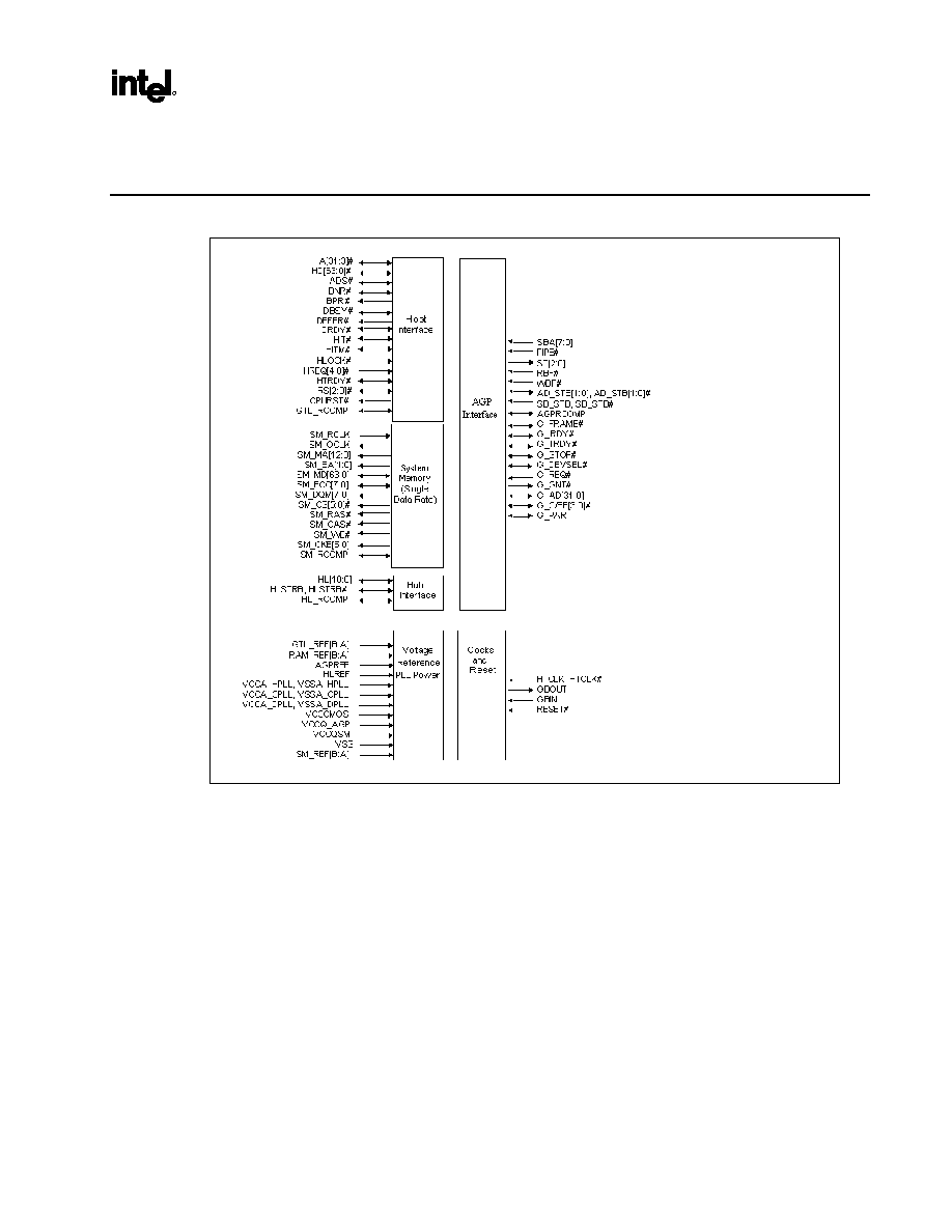
Figure 1. Intel 830MP Chipset Interface Block Diagram
Intel
Æ
830 Chipset Family
26 Datasheet
298338-003
R
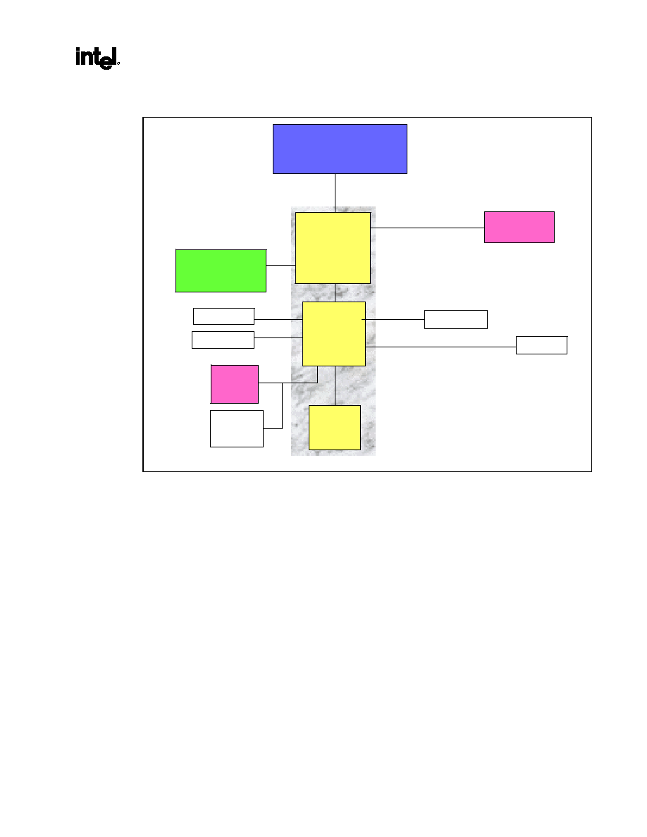
Figure 2. Intel 830M Chipset Interface Block Diagram
,
D ispla y
Interfa ce
S ystem
M em o ry
(S ingle
D ata R ate)
S M_ MA [12:0]
S M_B A [1 :0]
S M _M D [63:0 ]
S M _E C C[7:0 ]
S M _D Q M [7:0 ]
S M _C S [5:0]#
S M_RA S #
S M_CA S #
S M_W E #
S M_CK E [5:0]
S M_RC O M P
V S YN C
H S YNC
R E D
G R E E N
B LU E
R E FS E T
[RE D ,G R E E N ,B LU E#
A G P
Interfa ce
S B A [7:0]
P IP E #
S T[2:0]
R B F#
W B F#
A D _S TB [1:0], A D _S TB [1:0]#
S B _S TB , S B _S TB #
A G P R C O MP
G _FR A ME #
G _ IRD Y #
G _TR D Y#
G _S TO P #
G _D E VS E L#
G _R E Q #
G _G N T#
G _A D [31:0]
G _C /B E [3:0]#
G _P A R
H ost
Interfa ce
H A [31:3]#
H D [63:0]#
A D S #
B N R #
B P R I#
D B S Y#
D EFE R#
D R DY #
H IT#
HIT M #
H LO CK #
H R E Q [4:0]#
H TR DY#
RS [2:0 ]#
C P UR S T#
G TL_R C O MP
G TL_RE F[B :A ]
R A M_RE F[B :A ]
A G P RE F
H LR E F
V C C A _H P LL , V S S A _H PL L
V C C A _C P LL , V S S A _C PL L
V C C A _D P LL , V S S A _D PL L
V CC C M O S
V C C Q _A G P
V C C Q S M
V oltage
R efe rnce,
P LL P ow er
M ultiplexed with A G P
(either A G P o r
these functions)
Note: D ashed lines indicated m ultiple xed
functions.
H TC LK , HT CLK #
G BO U T
G BIN
G M _G CLK [R eserved ]
D RE FCLK
R E S E T#
C locks
and
R eset
Digital
V ideo
O ut A
(DV O A )
D VO A _C LK /D V O A _C LK
D V O A _D [11:0]
D VO A _H S YN C
DV O A _V S YN C
D V O A _B LA N K #
D VO A _R C O M P
D V O A _ INTR #
DV O A _C LK IN T
DV O A _FLD /S T L
H ub
Interface
H L[1 0:0]
H LS TR B , HLS TR B #
H L_RC O MP
DD C 2_DA T A
D DC 2 _C LK
I2 C _D A TA
I2C _C LK
D D C 1_D A TA
D D C 1_C LK
G P IO
D igital
Video
O ut C
(D V O C )
D V O C _C LK /D V O C _C LK
D V O C _D [11:0]
D V O C _H S YN C
D V O C _V S YN C
D V O C _B LA NK #
D V O B C _IN TR #
D V O C _FLD /S T L
MD DC _D A TA
MD DC _C LK
M I2C _D A TA
M I2C _CLK
M ultiplexed
G P IO
D Q _A [7:0] [Re served]
D Q _B [7:0] [Re served]
R Q [7:0] [R eserved]
C TM , C T M # [R eserved]
C FM , C FM # [R eserved]
C MD [R ese rved]
S C K [Reserved]
S IO [R eserved]
G raphics
Direct
R DR A M
C hannel
D igital
Video
O ut B
(D V O B )
D V O B _C LK /D V O B _C LK
D V O B _D[11:0]
D V O B _H S YN C
D V O B _V S YN C
D V O B _B LA N K #
D V O B C _C LK IN T
D V O B _F LD /S TL
S M_O C LK
S M_R C LK
V S S
S M_R E F[B :A ]
G M_ RC LK [R eserved]
(Reserved)
Intel
Æ
830 Chipset Family
298338-003 Datasheet
27
R
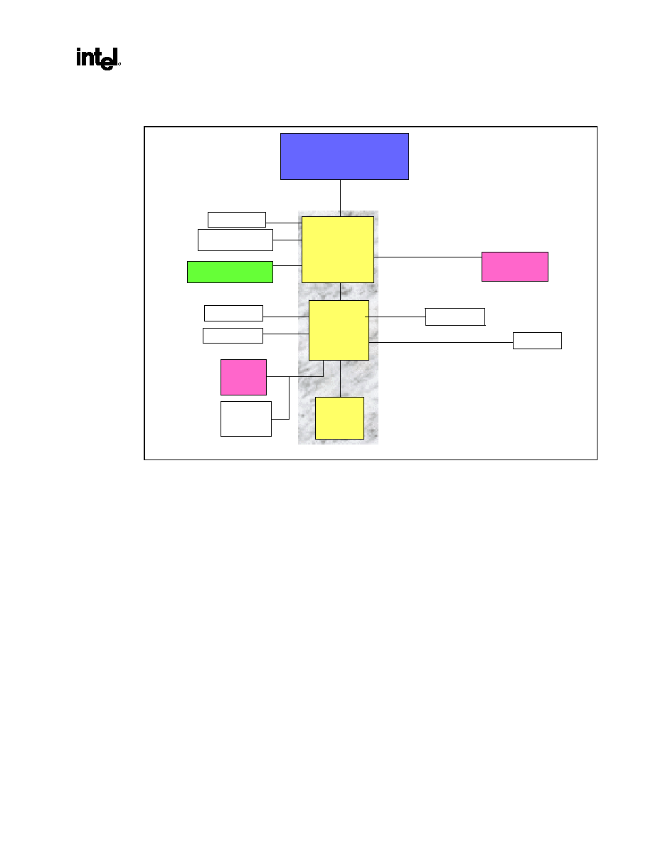
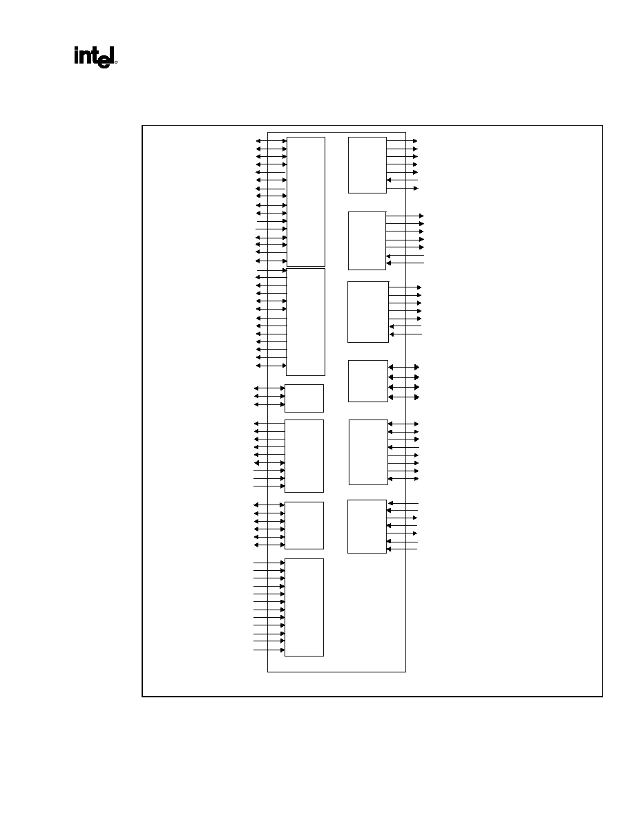
Figure 3. Intel 830MG Chipset Interface Block Diagram
Display
Interface
System
Memory
(Single
Data Rate)
SM_MA[12:0]
SM_BA[1:0]
SM_MD[63:0]
SM_ECC[7:0]
SM_DQM[7:0]
SM_CS[5:0]#
SM_RAS#
SM_CAS#
SM_WE#
SM_CKE[5:0]
SM_RCOMP
VSYNC
HSYNC
RED
GREEN
BLUE
REFSET
RED,GREEN,BLUE#
Host
Interface
HA[31:3]#
HD[63:0]#
ADS#
BNR#
BPRI#
DBSY#
DEFER#
DRDY#
HIT#
HITM#
HLOCK#
HREQ[4:0]#
HTRDY#
RS[2:0]#
CPURST#
GTL_RCOMP
GTL_REF[B:A]
RAM_REF[B:A]
AGPREF
HLREF
VCCA_HPLL, VSSA_HPLL
VCCA_CPLL, VSSA_CPLL
VCCA_DPLL, VSSA_DPLL
VCCCMOS
VCCQ_AGP
VCCQSM
Voltage
Refernce,
PLL Power
Digital
Video
Out A
(DVOA)
DVOA_CLK/DVOA_CLK
DVOA_HSYNC
DVOA_VSYNC
DVOA_BLANK#
DVOA_RCOMP
DVOA_INTR#
DVOA_CLKINT
DVOA_FLD/STL
Hub
Interface
HL[10:0]
HLSTRB, HLSTRB#
HL_RCOMP
DDC2_DATA
DDC2_CLK
I2C_DATA
I2C_CLK
DDC1_DATA
DDC1_CLK
GPIO
SM_OCLK
SM_RCLK
VSS
SM_REF[B:A]
DVOB_CLK/DVOB_CLK
DVOB_D[11:0]
DVOB_HSYNC
DVOB_VSYNC
DVOB_BLANK#
DVOBC_CLKINT
DVOB_FLD/STL
Digital
Video
OutB
(DVOB)
DVOC_CLK/DVOC_CLK
DVOC_D[11:0]
DVOC_HSYNC
DVOC_VSYNC
DVOC_BLANK#
DVOBC_INTR#
DVOC_FLD/STL
Digital
Video
OutC
(DVOC)
MDDC_DATA
MDDC_CLK
MI2C_DATA
MI2C_CLK
GPIO
DQ_A[7:0] [Reserved]
DQ_B[7:0] [Reserved]
RQ[7:0] [Reserved]
CTM, CTM# [Reserved]
CFM, CFM# [Reserved]
CMD [Reserved]
SCK [Reserved]
SIO [Reserved]
Graphics
Direct
RDRAM
Channel
HTCLK, HTCLK#
GBOUT
GBIN
GM_GCLK [Reserved]
DREFCLK
RESET#
Clocks
and
Reset
GM_RCLK [Reserved]
# DVOA_D[11:0]
(Reserved)

Intel
Æ
830 Chipset Family
28 Datasheet
298338-003
R
2.1 Terminology
82830MP Graphics and
Memory Controller Hub
(GMCH-M)
The Intel 830MP Graphics and Memory Controller Hub-Mobile component, which contains
the CPU interface, system SDRAM controller and AGP interface. It communicates with the
ICH3-M over a proprietary interconnect called the hub interface.
82830M Graphics and
Memory Controller Hub
(GMCH-M)
The Intel 830M Graphics and Memory Controller Hub-Mobile component which contains
the CPU interface, system SDRAM controller, AGP interface, and Integrated Graphics
Device (IGD). It communicates with the ICH3-M over a proprietary interconnect called the
hub interface.
82830MG Graphics and
Memory Controller Hub
(GMCH-M)
The Intel 830MG Graphics and Memory Controller Hub-Mobile component which contains
the CPU interface, system SDRAM controller, and Integrated Graphics Device (IGD). It
communicates with the ICH3-M over a proprietary interconnect called the hub interface.
Intel 830 Chipset Family
Intel 830 Chipset family SKU consists of the following 3 defined SKUs: 82830MP, 82830M,
82830MG and will be referred to as the Intel 830 Chipset Family
Discrete AGP Graphics
Interface
The Intel 830M and 830MP Graphics and Memory Controller Hub-Mobile (GMCH-M)
components which implements an external graphics solution (AGP) will be referred to as
Intel 830M and 830MP discrete AGP graphics Interface
Internal Graphics device
PCI Device #2 of the Intel 830M and 830MG Graphics and Memory Controller Hub-Mobile
(GMCH-M) component which implements the Intel Graphics solution will be referred to as
the Intel graphics device
82801CAM I/O
Controller Hub (ICH3-M)
The ICH3-M is connected to the GMCH-M through a proprietary interconnect called the hub
interface. This is the I/O Controller Hub or ICH component that contains the primary PCI
interface, LPC interface, USB1.1, ATA-100 and other IO functions.
Hub Interface
The proprietary interconnect between the GMCH-M and the ICH3-M. In this document, hub
interface cycles originating from or destined for the ICH3-M are generally referred to as hub
interface cycles. Hub cycles originating from or destined for the primary PCI interface on
the ICH3-M are sometimes referred to as Hub Interface/PCI cycles.
DVO Port
Digital Video Out Port. Refers to the Intel 830M and 830MG Chipset's digital display
channels. The Intel 830M Chipset has one dedicated DVO and two DVOs that are
multiplexed with AGP. The Intel 830MG Chipset has three dedicated DVO.
AGP
Accelerated Graphics Port. Refers to the AGP/PCI interface that is in the Intel 830MP and
830M Chipset SKUs. It supports a 1.5V AGP 4X component. PIPE# and SBA cycles are
generally referred to as AGP transactions. FRAME# cycles are generally referred to as
AGP/PCI transactions.
AGP/PCI1
The physical bus that is driven directly by the AGP/PCI1 Bridge (Device #1) in the 830MP
and 830M SKUs. This is the primary AGP bus.
Primary PCI
The primary physical PCI (PCI0) bus that is driven directly by the ICH3-M component. It
supports a 3.3V interface and is 5.0V tolerant, 33 MHz PCI 2.2 compliant components.
Interaction between PCI0 and GMCH-M occurs over the hub interface. Note that even
though the Primary PCI bus is referred to as PCI0 it is not PCI Bus #0 from a configuration
standpoint.
Secondary PCI
The secondary physical PCI (PCI1) interface that is a subset of the AGP bus driven directly
by the GMCH-M. It supports a subset of 1.5V, 66 MHz PCI 2.2 compliant components.
Note that even though the Secondary PCI bus is referred to as PCI1 it may not be
configured as PCI Bus #1.
Direct AGP
Integrated AGP interface.
UMA
Unified Memory Architecture. Graphics memory for the IGD that is located in system
memory
IGD
Integrated Graphics Device. The Graphics Device that is internal to the GMCH-M
DVMT
Direct Video Memory Technology

Intel
Æ
830 Chipset Family
298338-003 Datasheet
29
R
2.2
Intel 830 Chipset Family
System Architecture
The Intel 830 Chipset family (consists of the three different SKUs: 82830M, 82830MP, 82830MG)
is a
highly integrated hub that provides the CPU interface to a Mobile Intel
Æ
Pentium
Æ
III
Processor-M /
Mobile Intel Celeron Processor, the SDRAM system memory interface, a hub link interface to the
82801CAM I/O Controller Hub
(
ICH3-M), and is optimized for Mobile Intel Pentium
III
Processor-M
/Mobile Intel Celeron Processor configurations at 133-MHz PSB.
2.2.1
Intel 830MP Chipset
The Intel 830MP Chipset supports Mobile Intel Pentium
III
Processor-M / Mobile Intel Celeron
Processors with an external AGP 4X graphics solution.
∑
1.25-V AGTL host bus supporting 32-bit host addressing
∑
System SDRAM supports PC133 (LVTTL) SDRAM
∑
Supports up to 1.0 GB of system SDRAM
∑
AGP interface with 1x/2x/4x SBA/Data Transfer and 2x/4x Fast Write capability
∑
Hub interface to ICH3-M
2.2.2
Intel 830M Chipset
The Intel 830M Chipset has integrated graphics capabilities as well as external AGP support. Its
dedicated multimedia engines deliver high performance 3D, 2D, video, and display capabilities. The
Intel 830M Chipset provides the flexibility of an external graphics solution with the AGP port.
∑
1.25-V AGTL host bus supporting 32-bit host addressing
∑
System SDRAM supports PC133 (LVTTL) SDRAM
∑
Supports up to 1.0 GB of system SDRAM
∑
AGP interface with 1x/2x/4x SBA/Data Transfer and 2x/4x Fast Write capability
∑
Hub interface to ICH3-M
∑
Integrated graphics capabilities, including 3D rendering acceleration and 2D hardware acceleration
∑
Integrated 350-MHz RAMDAC
∑
A variety of display device protocols (TV, DVI, LVDS) are supported through Digital Video Out
Ports (one dedicated and two muxed with AGP) connected to external devices
2.2.3
Intel 830MG Chipset
The Intel 830MG Chipset has integrated graphics capabilities. Its dedicated multimedia engines deliver
high performance 3D, 2D, video, and display capabilities. 1.25-V AGTL host bus supporting 32-bit host
addressing:
∑
1.25-V AGTL host bus supporting 32-bit host addressing
∑
System SDRAM supports PC133 (LVTTL) SDRAM
∑
Supports up to 1.0 GB of system SDRAM
∑
Hub interface to ICH3-M

Intel
Æ
830 Chipset Family
30 Datasheet
298338-003
R
∑
Integrated graphics capabilities, including 3D rendering acceleration and 2D hardware acceleration
∑
Integrated 350-MHz RAMDAC
∑
A variety of display device protocols (TV, DVI, LVDS) are supported through three Digital Video
Out Ports (DVOs) connected to external devices
2.3
Intel 830 Chipset Family Host Interface
1
The Intel 830 Chipset family is optimized for the Mobile Intel Pentium
III
Processor-M /Mobile Intel
Celeron Processors. Each member of the Intel 830 Chipset family supports a PSB frequency of 133 MHz
using 1.25-V AGTL signaling. Dual ended termination AGTL is supported for single processor
configurations. It supports 32-bit host addressing, decoding up to 4 GB of the CPU's memory address
space. Host initiated I/O cycles are decoded to AGP/PCI1, Hub interface, or GMCH-M configuration
space. Host initiated memory cycles are decoded to AGP/PCI1, Hub interface, or system SDRAM. All
memory accesses from the Host interface that hit the graphics aperture are translated using an AGP
address translation table. GMCH-M accesses to graphics memory and AGP/PCI1 device accesses to
non-cacheable system memory are not snooped on the host bus. Memory accesses initiated from
AGP/PCI1 using PCI semantics and from Hub interface to system SDRAM will be snooped on the host
bus.
Note: Discrete AGP support is available only with the Intel 830MP and 830M Chipset.
2.4
Intel 830 Chipset Family System Memory Interface
The Intel 830 Chipset family integrates a system memory SDRAM controller with a 64-bit wide
interface. The Intel 830 Chipset family supports Single Data Rate (SDR) SDRAM for system memory.
Consequently, the GMCH-M system memory buffers support LVTTL signal interfaces.
Configured for SDRAM, the GMCH-M memory interface includes support for the following:
∑
Up to 1.0 GB of 133-MHz SDR SDRAM using 512-Mb technology
∑
PC133 SO-DIMMs
∑
Maximum of two SO-DIMMs, single-sided and/or double-sided
∑
The Intel 830M Chipset only supports four bank memory technologies.
∑
Four Integrated Clock buffers
2.5
Intel 830M / 830MP Discrete AGP Interface
GMCH-M has the capability to support a single AGP or PCI-66 component using the Intel 830M and
830MP AGP interface via an AGP 2.0 interface. High bandwidth access to data is provided through the
system memory ports. GMCH-M can access AGP memory located in system memory with a peak
bandwidth of 1.0 GB/s. Actual AGP throughput may vary depending on application running and system
memory throttling mechanism applied. Please consult Section 5.7.11.2 for a discussion on throttling
management.
The 830M/830MP AGP port supports a 1.5-V interface and is not 3.3-V safe. This mode is compliant
with the AGP 2.0 spec.

Intel
Æ
830 Chipset Family
298338-003 Datasheet
31
R
The AGP/PCI1 interface supports up to 4x AGP signaling and up to 4x Fast Writes. AGP semantic
cycles to system SDRAM are not snooped on the host bus. PCI semantic cycles to system SDRAM are
snooped on the host bus. The GMCH-M supports PIPE# or SBA[7:0] AGP address mechanisms, but not
both simultaneously. Either the PIPE# or the SBA[7:0] mechanism must be selected during system
initialization. The GMCH-M contains a 32-deep AGP request queue. High priority accesses are
supported.
2.6
Intel 830M / 830MG Internal Graphics Introduction
The Intel 830M and 830MG Chipset IGD provide a highly integrated graphics accelerator delivering
high performance 3D, 2D, and video capabilities. The GMCH-M contains an extensive set of
instructions for 3D operations, BLT and Stretch BLT operations, motion compensation, overlay, and
display control. GMCH-M supports a UMA architecture using DVMT configuration. With its interfaces
to analog display and flat panel display (through an accompanying LVDS transmitter/scaler), the
GMCH-M provides a complete graphics solution.
High bandwidth access to data is provided through the system memory ports. The GMCH-M uses tiling
architecture to increase memory efficiency and thus maximize effective rendering bandwidth. The
GMCH-M uses Intel's Direct Memory Execution model to fetch textures from system memory at 1.0
GB/s. GMCH-M includes a cache controller to avoid frequent memory fetches of recently used texture
data.
The GMCH-M also provides 2D hardware acceleration for block transfers of data (BLTs). The BLT
engine provides the ability to copy a source block of data to a destination and perform raster operations
(e.g., ROP1, ROP2, and ROP3) on the data using a pattern, and/or another destination. Performing these
common tasks in hardware reduces CPU load, and thus improves performance.
2.7
Intel 830M / 830MG Internal Graphics Display Interface
The Intel 830M and 830MG IGD SKU have four display ports, one analog and three digital. This
provides support for a progressive scan analog monitor, a dedicated DVO port (DVOA) and dual DVO
ports. Each port can transmit data according to one or more protocols. The DVO ports are connected to
an external device that converts one protocol to another. Examples of this are TV encoders, external
DACs, LVDS transmitters, and TMDS transmitters. Each display port has control signals that may be
used to control, configure and/or determine the capabilities of an external device. The data that is sent
out the display port is selected from one of the two possible sources; pipe A or pipe B.
2.7.1
Intel 830M and 830MG Analog Display Port
The Intel
830M and
830MG Chipset has an integrated 350-MHz RAMDAC that can directly drive a
progressive scan analog monitor up to a resolution of 1800 x 1440 pixels.
2.7.2
Intel 830M and 830MG DVO interfaces
The Intel 830M and 830MG Chipset provides digital display channels that are capable of driving a 165-
MHz pixel clock. GMCH-M is compliant with DVI Specification 1.0. When combined with a DVI
compliant external device and connector, the Intel 830M and 830MG Chipset has a high-speed interface
to a digital display (e.g. flat panel or digital CRT).

Intel
Æ
830 Chipset Family
32 Datasheet
298338-003
R
2.7.2.1
Intel 830M and 830MG Dedicated DVOA Interface
The Intel 830M and 830MG supports DVO devices that can drive pixel clocks up to 165 MHz. The
dedicated DVOA interface can support a variety of TV-Out and TMDS transmitters.
2.7.2.2
Intel 830M and 830MG DVOB and DVOC Interfaces
The Intel 830MG Chipset has dedicated interfaces (DVOB and DVOC). Each interface is capable to
drive pixel clocks up to 165 MHz. The DVO interface can support a variety of TV-Out and TMDS
transmitters. The DVOB and DVOC interfaces may be used independently or combined to support
higher resolutions and refresh rates.
Similar to the Intel 830MG Chipset, the Intel 830M Chipset can use DVOB and DVOC interfaces
independently or combined for higher resolutions and refresh rates. Furthermore, the Intel 830M
Chipset supports a discrete AGP graphics device by multiplexing an AGP interface with the DVOB and
DVOC interfaces.

Intel
Æ
830 Chipset Family
298338-003 Datasheet
33
R
3 Signal
Description
This section provides a detailed description of the Intel 830 Chipset family GMCH-M signals. The
signals are arranged in functional groups according to their associated interface.
The "#" symbol at the end of a signal name indicates that the active, or asserted state occurs when the
signal is at a low voltage level. When "#" is not present after the signal name the signal is asserted when
at the high voltage level.
When not otherwise specified, "set" refers to changing a bit to its asserted state (a logical 1). Clear
refers to changing a bit to its negated state (a logical 0). The following notations are used to describe the
signal type:
The following notations are used to describe the signal type:
I
Input
pin
O Output
pin
I/O
Bi-directional Input/Output pin
s/t/s
Sustained Tristate. This pin is driven to its inactive state prior to tri-stating.
as/t/s
Active Sustained Tristate. This applies to some of the Hub interface signals. This pin
is weekly driven to its last driven value.
The signal description also includes the type of buffer used for the particular signal:
AGTL
Open Drain 1.25-V AGTL interface signal. Refer to the AGTL I/O Specification for
complete details. AGTL signals are "inverted bus" style where a low voltage
represents a logical "1".
AGP/1.5V
Signals used for AGP or 1.5V interfaces. AGP signals are compatible with AGP 2.0
1.5-V Signaling Environment DC and AC Specifications. The buffers are not 3.3-V
tolerant.
LVTTL
Low Voltage TTL compatible signals. These are also 3.3-V outputs.
CMOS
CMOS
buffers.
Note that CPU address and data bus signals are logically inverted signals. In other words, the actual
values are inverted of what appears on the CPU bus. This must be taken into account and the addresses
and data bus signals must be inverted inside the GMCH-M. All CPU control signals follow normal
convention. A 0 indicates an active level (low voltage) if the signal is followed by # symbol and a 1
indicates an active level (high voltage) if the signal has no # suffix.
Table 1 shows the Vtt/Vdd and Vref levels for the various interfaces.

Intel
Æ
830 Chipset Family
34 Datasheet
298338-003
R
Table 1. Signal Voltage Levels
Interface Vtt/Vdd
(nominal) Vref
AGTL
1.25 V
2/3 * Vtt
1.5 V/AGP
1.5 V
0.5 * Vdd
LVTTL
3.3 V
Vddq * 0.5
RSL [Reserved]
1.8 V
1.4 V
Hub Interface
1.8 V
0.5 * Vdd

Intel
Æ
830 Chipset Family
298338-003 Datasheet
35
R
3.1
Common Signals for the Intel 830 Chipset Family
This section describes the common signals that apply to the entire Intel 830 Chipset family. The Intel
830 Chipset family common signals consist of: Host Interface signals, System Memory signals, Hub
Interface signals, and Clock and Reset Signals.
3.1.1
Host Interface Signals
Table 2. Host Interface Signal Descriptions
Signal Name
Type
Description
CPURST# O
AGTL
CPU Reset. The CPURST# pin is an output from the GMCH-M. The GMCH-M
asserts CPURST# while RESET# (PCIRST# from ICH3-M) is asserted and for
approximately 1 ms after RESET# is deasserted. The CPURST# allows the CPUs
to begin execution in a known state.
Note that the ICH3-M must provide CPU strap set-up and hold times around
CPURST#. This requires strict synchronization between GMCH-M CPURST#
deassertion and ICH3-M driving the straps.
HA[31:3]# I/O
AGTL
Host Address Bus: HA[31:3]# connect to the CPU address bus. During CPU
cycles the HA[31:3]# are inputs. The GMCH-M drives HA[31:3]# during snoop
cycles on behalf of hub interface and AGP/Secondary PCI initiators. Note that the
address bus is inverted on the CPU bus.
HD[63:0]# I/O
AGTL
Host Data: These signals are connected to the CPU data bus. Note that the data
signals are inverted on the CPU bus.
ADS# I/O
AGTL
Address Strobe: The CPU bus owner asserts ADS# to indicate the first of two
cycles of a request phase.
BNR# I/O
AGTL
Block Next Request: Used to block the current request bus owner from issuing a
new request. This signal is used to dynamically control the CPU bus pipeline depth.
BPRI# O
AGTL
Priority Agent Bus Request: The GMCH-M is the only Priority Agent on the CPU
bus. It asserts this signal to obtain the ownership of the address bus. This signal
has priority over symmetric bus requests and will cause the current symmetric
owner to stop issuing new transactions unless the HLOCK# signal was asserted.
DBSY# I/O
AGTL
Data Bus Busy: Used by the data bus owner to hold the data bus for transfers
requiring more than one cycle.
DEFER# O
AGTL
Defer: GMCH-M will generate a deferred response as defined by the rules of the
GMCH-M's dynamic defer policy. The GMCH-M will also use the DEFER# signal to
indicate a CPU retry response.
DRDY# I/O
AGTL
Data Ready: Asserted for each cycle that data is transferred.
HIT# I/O
AGTL
Hit: Indicates that a caching agent holds an unmodified version of the requested
line. Also, driven in conjunction with HITM# by the target to extend the snoop
window.
HITM# I/O
AGTL
Hit Modified: Indicates that a caching agent holds a modified version of the
requested line and that this agent assumes responsibility for providing the line.
Also, driven in conjunction with HIT# to extend the snoop window.
HLOCK# I
AGTL
Host Lock: All CPU bus cycles sampled with the assertion of HLOCK# and ADS#,
until the negation of HLOCK# must be atomic, i.e. no hub interface or AGP/PCI
snoopable access to SDRAM is allowed when HLOCK# is asserted by the CPU.

Intel
Æ
830 Chipset Family
36 Datasheet
298338-003
R
HREQ[4:0]# I/O
AGTL
Host Request Command: Asserted during both clocks of request phase. In the
first clock, the signals define the transaction type to a level of detail that is sufficient
to begin a snoop request. In the second clock, the signals carry additional
information to define the complete transaction type. The transactions supported by
the GMCH-M Host Bridge are defined in the Host Interface section of this
document.
HTRDY# I/O
AGTL
Host Target Ready: Indicates that the target of the CPU transaction is able to
enter the data transfer phase.
RS[2:0]# I/O
AGTL
Response Signals: Indicates type of response according to the following table:
RS[2:0] Response type
000 Idle state
001 Retry response
010 Deferred response
011 Reserved (not driven by GMCH-M)
100 Hard Failure (not driven by GMCH-M)
101 No data response
110 Implicit Writeback
111 Normal data response
GTL_RCOMP I/O
GTL Compensation: Used to calibrate the GTL interface buffers to match the
board. This pin should be connected to an 80-
simple resistor to ground.
Total pins for this section: 113.

Intel
Æ
830 Chipset Family
298338-003 Datasheet
37
R
3.1.2 System
Memory
Interface
Table 3. System Memory Interface Signal Descriptions
Signal Name
Type
Description
SM_MA[12:0] O
LVTTL
Memory Address: SM_MA[12:0] are used to provide the multiplexed row and
column address to SDRAM.
SM_BA[1:0] O
LVTTL
Memory Bank Address: These signals define the banks that are selected within
each SDRAM row. The SM_MA and SM_BA signals combine to address every
possible location within a SDRAM device.
SM_MD[63:0] I/O
LVTTL
Memory Data: These signals are used to interface to the SDRAM data bus.
SM_DQM[7:0] O
LVTTL
Input/Output Data Mask: These pins act as synchronized output enables during
read cycles and as byte enables during write cycles.
SM_CS[3:0]# O
LVTTL
Chip Select: For the memory rows configured with SDRAM, these pins perform the
function of selecting the particular SDRAM components during the active state.
Note: There is one SM_CS per SDRAM row. These signals can be toggled on every
rising System Memory Clock edge.
SM_RAS# O
LVTTL
SDRAM Row Address Strobe: A table of the SDRAM commands supported by the
Intel 830 Chipset family is given in the SDRAM section. SM_RAS# may be heavily
loaded and requires 2 SDRAM clock cycles for setup time to the SDRAMs.
SM_CAS# O
LVTTL
SDRAM Column Address Strobe: A table of the SDRAM commands supported by
the Intel 830 Chipset family is given in the SDRAM section. SM_CAS# may be
heavily loaded and requires 2 SDRAM clock cycles for setup time to the SDRAMs.
SM_WE# O
LVTTL
Write Enable Signal: SM_WE# is asserted during writes to SDRAM. Refer to truth
table of the SDRAM commands supported by the Intel 830 Chipset family, given in
the SDRAM section. SM_WE# may be heavily loaded and requires 2 SDRAM clock
cycles for setup time to the SDRAMs.
SM_CKE[3:0] O
LVTTL
Clock Enable: These signals are used to signal a self-refresh or power down
command to a SDRAM array when entering system suspend. SM_CKE is also used
to dynamically power down inactive SDRAM rows. There is one SM_CKE per
SDRAM row. These signals can be toggled on every rising SM_CLK Clock edge.
SM_OCLK O
LVTTL
System Memory Output Clock: This signal delivers a synchronized clock to the
SM_RCLK pin.
SM_RCLK I
LVTTL
System Memory Return Clock: This signal receives the synchronized clock from
SM_OCLK.
SM_CLK [3:0]
O
LVTTL
System Memory Clock: These signals deliver a synchronized clock to the
SDRAMs.
SM_RCOMP I/O
System Memory RCOMP: Used to calibrate the system memory I/O buffers. This
pin should be connected to a 27.5-
resistor tied to Vss.
Total pins for System Memory Section: 105.

Intel
Æ
830 Chipset Family
38 Datasheet
298338-003
R
3.1.3
Hub Interface Signals
Table 4. Hub Interface Signal Descriptions
Signal
Name
Type Description
HL[10:0] I/O
(as/t/s)
CMOS
HL[10:0] Hub Interface Signals. Signals used for the hub interface.
HLSTRB;
HLSTRB#
I/O
(as/t/s)
CMOS
HLSTRB; HLSTRB# Hub Interface Strobe/Complement. The two differential strobe
signals used to transmit or receive packet data.
HL_RCOMP I/O HL_RCOMP Hub Interface Compensation: Used to calibrate the hub I/O buffers. This
signal has an external 55-ohm pull-down resistor.
Total pins for this section: 14.
3.1.4
Clocking and Reset
Table 5. Clocking and Reset Signal Descriptions
Signal Name
Type
Description
HTCLK;
HTCLK#
I
CMOS
Host Clock In: These pins receive a buffered host clock from the external clock
synthesizer. This clock is used by all of the GMCH-M. The clock is also the reference
clock for the graphics core PLL. This is a low voltage differential input.
GBOUT O
LVTTL
AGP/Hub Clock Reference Output: This clock goes to the external AGP/Hub/PCI
buffer.
GBIN I
LVTTL
AGP/Hub Input Clock: 66 MHz, 3.3-V input clock from external buffer AGP/Hub-link
interface.
GM_GCLK;
GM_RCLK
O
CMOS
Graphics Memory Clock Out: (Reserved)These signals should leave as NC ("Not
Connected").
DCLKREF I
LVTTL
Display Clock Input: This pins provides a 48-MHz input clock to the Display PLL that
is used for 2D/Video/Flat Panel and DAC.
The signal needs pull down if ext graphics solution is implemented.
RESET# I
LVTTL
Reset In: When asserted, this signal will asynchronously reset the GMCH-M logic.
This signal is connected to the PCIRST# output of the ICH3-M. The ICH3-M drives this
to 3.3 V. All AGP/PCI output and bi-directional signals will also tri-state compliant to
PCI rev 2.2 specifications. This input should have a Schmidt trigger to avoid spurious
resets.
Note that this input needs to be 3.3-V tolerant.
Total pins for Clocks/Resets section: 8.

Intel
Æ
830 Chipset Family
298338-003 Datasheet
39
R
3.1.5 Reserved
Signals
Table 6. Intel Reserved Signals
Signal
Name
Type Description
DQ_A[7:0]
Intel Reserved. Should be left NC ("Not Connected")
DQ_B[7:0]
Intel Reserved. Should be left NC ("Not Connected")
RQ[7:0]
Intel Reserved. Should be left NC ("Not Connected")
CTM;CTM#
Intel Reserved . Requires pull down.
CFM;CFM#
Intel Reserved. Should be left NC ("Not Connected")
CMD
Intel Reserved. Should be left NC ("Not Connected")
SCK
Intel Reserved. Should be left NC ("Not Connected")
SIO
Intel Reserved. Should be left NC ("Not Connected")
Total reserved pins: 31.

Intel
Æ
830 Chipset Family
40 Datasheet
298338-003
R
3.2
Common Signals for 830M and 830MP Chipset Discrete
AGP Graphics Implementation
The Intel 830M and 830MP Chipset support an external AGP graphics solution. The following signals
apply only when an external AGP graphics solution is implemented. Please consult Section 3.3 for
internal graphics implementation with the Intel 830M and 830MG Chipset. For signal multiplexing
information between AGP and DVO/Display signals, please refer to Sections 3.3.3.1and 3.3.5.2. Please
see Intel
Æ
830 Chipset Family Design Guide for design recommendations required for pins where NO
functionality is defined for the chosen SKU.
3.2.1 AGP
Addressing
Signals
Table 7. AGP Addressing Signal Descriptions
Signal
Name
Type Description
PIPE#
I
AGP
Pipelined Read: This signal is asserted by the current master to indicate a full width
address is to be queued by the target. The master queues one request each rising clock
edge while PIPE# is asserted. When PIPE# is deasserted no new requests are queued
across the AD bus. PIPE# is a sustained tri-state signal from the master (graphics
controller) and is an input to the GMCH-M.
SBA[7:0] I
AGP
Sideband Address: This bus provides an additional bus to pass address and command
to the GMCH-M from the AGP master.
The above table contains two mechanisms to queue requests by the AGP master. Note that the master
can only use one mechanism. When PIPE# is used to queue addresses, the master is not allowed to
queue addresses using the SBA bus. For example, during configuration time, if the master indicates that
it can use either mechanism, the configuration software will indicate which mechanism the master will
use. Once this choice has been made, the master will continue to use the mechanism selected until the
master is reset (and reprogrammed) to use the other mode. This change of modes is not a dynamic
mechanism but rather a static decision when the device is first being configured after reset.

Intel
Æ
830 Chipset Family
298338-003 Datasheet
41
R
3.2.2
AGP Flow Control Signals
Table 8. AGP Flow Control Signal Descriptions
Signal Name
Type
Description
RBF# I
AGP
Read Buffer Full: Indicates if the master is ready to accept previously requested low
priority read data.
When RBF# is asserted, the GMCH-M is not allowed to return low priority read data to
the AGP master on the first block. RBF# is only sampled at the beginning of a cycle. If
the AGP master is always ready to accept return read data, it is not required to
implement this signal.
WBF# I
AGP
Write Buffer Full: Indicates if the master is ready to accept fast write data from the
GMCH-M.
When WBF# is asserted, the GMCH-M is not allowed to drive fast write data to the
AGP master. WBF# is only sampled at the beginning of a cycle. If the AGP master is
always ready to accept fast write data, it is not required to implement this signal.
3.2.3
AGP Status Signals
Table 9. AGP Status Signal Descriptions
Signal Name
Type
Description
ST[2:0] O
AGP
Status: Provides information from the arbiter to the AGP Master on what it may
do.
ST[2:0] only have meaning to the master when its GNT# is asserted. When
GNT# is deasserted these signals have no meaning and must be ignored.
000 Indicates that previously requested low priority read data is being
returned.
001 Indicates that previously requested high priority read data is being
returned.
010 Indicates that the master is to provide low priority write data for a
previously queued write command.
011 Indicates that the master is to provide high priority write data for a
previously queued write command.
100 Reserved
101 Reserved
110 Reserved
111 Indicates that the master has been given permission to start a bus
transaction. The master may queue AGP requests by asserting PIPE# or
start a PCI transaction by asserting FRAME#. ST[2:0] are always an
output from the GMCH-M and an input to the master.
AGP_RCOMP I/O
AGP RCOMP: Used to calibrate AGP I/O buffers for 830M and 830MP discrete
AGP interface
Please refer to the Intel
Æ
830 Chipset Family Design Guide for pull down resistor
value.

Intel
Æ
830 Chipset Family
42 Datasheet
298338-003
R
3.2.4
AGP Clocking Signals ≠ Strobes
Table 10. AGP Clock Signal-Strobe Descriptions
Signal
Name
Type Description
AD_STB0 I/O
(s/t/s)
AGP
AD Bus Strobe-0: Provides timing for 2x and 4x clocked data on AD[15:0] and
C/BE[1:0]#. The agent that is providing data drives this signal.
AD_STB0# I/O
(s/t/s)
AGP
AD Bus Strobe-0 Complement: The differential complement to the AD_STB0 signal. It
is used to provide timing for 4x clocked data.
AD_STB1 I/O
(s/t/s)
AGP
AD Bus Strobe-1: Provides timing for 2x and 4x clocked data on AD[31:16] and
C/BE[3:2]#. The agent that is providing data drives this signal.
AD_STB1# I/O
(s/t/s)
AGP
AD Bus Strobe-1 Complement: The differential complement to the AD_STB1 signal. It
is used to provide timing for 4x clocked data.
SB_STB I
AGP
Sideband Strobe: Provides timing for 2x and 4x clocked data on the SBA[7:0] bus. The
AGP master drives it after the system has been configured for 2x or 4x clocked sideband
address delivery.
SB_STB# I
AGP
Sideband Strobe Complement: The differential complement to the SB_STB signal. It is
used to provide timing for 4x clocked data.

Intel
Æ
830 Chipset Family
298338-003 Datasheet
43
R
3.2.5
PCI Signals - AGP Semantics
PCI signals are redefined when used in AGP transactions that are carried using AGP protocol extension.
For transactions on the AGP interface that are carried using PCI protocol, these signals completely
preserve PCI 2.2 semantics. The exact roles of all PCI signals during AGP transactions are defined
below.
Table 11. PCI Signals ≠ AGP Semantics Signal Descriptions
Signal Name
Type
Description
G_FRAME# I/O
s/t/s
AGP
Not used during an AGP pipelined transaction.
G_FRAME# is an output from the GMCH-M during Fast Writes.
G_IRDY# I/O
s/t/s
AGP
G_IRDY# indicates the AGP compliant master is ready to provide all write data
for the current transaction.
Once IRDY# is asserted for a write operation, the master is not allowed to insert
wait states. The assertion of IRDY# for reads indicates that the master is ready
to transfer to a subsequent block (32 bytes) of read data. The master is never
allowed to insert a wait state during the initial data transfer (32 bytes) of a read
transaction. However, it may insert wait states after each 32-byte block is
transferred. (There is no G_FRAME# -- G_IRDY# relationship for AGP
transactions.)
For Fast Write transactions, G_IRDY# is driven by the GMCH-M to indicate
when the write data is valid on the bus. The GMCH-M deasserts this signal to
insert wait states on block boundaries.
G_TRDY# I/O
s/t/s
AGP
G_TRDY# indicates the AGP compliant target is ready to provide read data for
the entire transaction (when the transfer size is less than or equal to 32 bytes)
or is ready to transfer the initial or subsequent block (32 bytes) of data when the
transfer size is greater than 32 bytes.
The target is allowed to insert wait states after each block (32 bytes) is
transferred on both read and write transactions.
For Fast Write transactions, the AGP master uses this signal to indicate when it
is willing to transfer a subsequent block.
G_STOP# I/O
s/t/s
AGP
G_STOP# Not used during an AGP transaction.
For Fast Write transactions G_STOP# is used to signal Disconnect or Target
Abort terminations.
G_DEVSEL# I/O
s/t/s
AGP
G_DEVSEL# Not used during an AGP transaction.
For Fast Write transactions, it is used when the transaction cannot complete
during the block.
G_REQ# I
AGP
G_REQ# Used to request access to the bus to initiate a PCI or AGP request.
G_GNT# O
AGP
G_GNT# Same meaning as PCI but additional information is provided on
ST[2:0].
The additional information indicates that the selected master
∑
Is the recipient of previously requested read data (high or normal priority)
∑
Is to provide write data (high or normal priority), for a previously queued write
command or
∑
Has been given permission to start a bus transaction (AGP or PCI).
G_AD[31:0] I/O
G_AD[31:0] Same as PCI.

Intel
Æ
830 Chipset Family
44 Datasheet
298338-003
R
AGP
G_C/BE[3:0]# I/O
AGP
G_C/BE[3:0]# Slightly different meaning.
∑
Provides command information (different commands than PCI) when
requests are being queued when using PIPE#.
∑
Provide valid byte information during AGP write transactions and are not
used during the return of read data.
G_PAR I/O
AGP
G_PAR Same as PCI. Not used on AGP transactions but used during PCI
transactions as defined by the PCI specification.
NOTES:
1. PCIRST# from the ICH3-M is connected to RESET# and is used to reset AGP interface logic within the GMCH-
M. The AGP agent will also use PCIRST# provided by the as an input to reset its internal logic.
2. LOCK# signal is not supported on the AGP interface (even for PCI operations).
3. The SERR# and PERR# signals are not supported on the AGP interface.
Total pins for AGP section: 66.
3.2.6
PCI Pins During PCI Transactions on AGP Interface
PCI signals described in a previous table behave according to PCI 2.2 specifications when used to
perform PCI transactions on the AGP Interface.

Intel
Æ
830 Chipset Family
298338-003 Datasheet
45
R
3.3
Common Signals for 830M and 830MG Chipset Internal
Graphics Implementation
An internal graphics device is available with the Intel 830M and 830MG Chipset. The following signals
apply when the internal graphics device is chosen. The internal graphics device has support for
Dedicated Digital Video Port (DVOA), Dual DVOB and DVOC ports, and Analog Display. Please
consult Section 3.2 for discrete AGP implementation with 830M or 830MP Chipset. Also see Sections
3.3.3.1 and 3.3.5.2 for signal mapping information between discrete AGP and DVO/Display signals for
the 830M SKU. Please refer to the Intel
Æ
830 Chipset Family Design Guide regarding design
recommendations for pins where no functionality is defined for the chosen SKU.
Table 12. Internal Graphics Status Signal Descriptions
Signal
Name
Type Description
AGP_BUSY# OD AGP_BUSY#: Output of the Intel 830M or 830MG GMCH-M graphics controller to the
ICH3-M, which indicates that certain internal graphics (IGD) activity is taking place.
Assertion indicates to the ACPI software to not enter the C3 state. Assertion also
causes a C3 exit if C3 was being entered, or was already entered when AGP_BUSY#
went active. AGP_BUSY# will be inactive when the graphics controller is in any ACPI
state other than D0.
AGP_BUSY# must be pulled up to a voltage rail which turned off in the ACPI S3-S5
stages.
.

Intel
Æ
830 Chipset Family
46 Datasheet
298338-003
R
3.3.1
Dedicated Digital Video Port (DVOA)
Table 13. Dedicated Digital Video Port (DVOA) Signal Descriptions
Name Type
Description
DVOA_CLK;
DVOA_CLK#
O
1.5 V
DVO Clock Output: These pins provide a differential pair reference clock that
can run up to 165 MHz.
DVOA_CLK (DVOCLKOUT0) (AJ24) corresponds to the primary clock out.
DVOA_CLK# (DVOCLKOUT1) (AG24) corresponds to the primary clock out.
DVOA_CLK and DVOA_CLK# need to be pulled up if:
i) The signals are NOT used when using internal graphics device, or
ii) Discrete AGP device is implemented.
DVOA_D[11:0] O
1.5 V
DVO Data: This data bus is used to drive 12-bit RGB data on each edge of
DVOA_CLKOUT. This provides 24-bits of data per clock.
DVOA_D[11:0] should be left as NC (not connected) if:
i) The signals are NOT used when using internal graphics device, or
ii) Discrete AGP device is implemented.
DVOA_HSYNC O
1.5 V
Horizontal Sync: HSYNC signal for the DVO interface. The active polarity of
the signal is programmable.
DVOA_HYSNC should be left as NC (not connected) if:
i) The signal is NOT used when using internal graphics device, or
ii) Discrete AGP device is implemented.
DVOA_VSYNC O
1.5V
Vertical Sync: VSYNC signal for the DVO interface. The active polarity of the
signal is programmable.
DVOA_VSYNC should be left as NC (not connected) if:
i) The signal is NOT used when using internal graphics device, or
ii) Discrete AGP device is implemented.
DVOA_BLANK# O
1.5 V
Flicker Blank or Border Period Indication: DVOA_BLANK# is a
programmable output pin driven by the GMCH-M.
When programmed as a blank period indication, this pin indicates active pixels
excluding the border.
When programmed as a border period indication, this pin indicates active pixel
including the border pixels.
DVOA_BLANK# should be left as NC (not connected) if:
i) The signal is NOT used when using internal graphics device, or
ii) Discrete AGP device is implemented.
DVOA_RCOMP I/O
DVO Compensation: Used to calibrate the DVOA I/O buffers. This signal
needs to be pulled down to ground through an external resistor (resistance is
based on board impedance).
DVOA_INTR# I
1.5 V
DVO Interrupt: This pin is used to signal an interrupt, typically used to indicate
a hot plug or unplug of a digital display.
DVOA_INTR# needs to be pulled up if:
i) The signal is NOT used when using internal graphics device, or
ii) Discrete AGP device is implemented.
DVOA_CLKINT I
1.5 V
DVO Pixel Clock Input/Interrupt input pin can be programmed to be either a
reference input to a dot clock PLL (DPLL) or to be a second interrupt input.
DVO Pixel Clock Input: When used as a pixel clock input, this signal may be
selected as a reference input for an external TV encoder.

Intel
Æ
830 Chipset Family
298338-003 Datasheet
47
R
DVO Interrupt: When used as an interrupt input, the signal is internally
ANDed with the DVOA_INTR# signal inside the GMCH-M.
DVOA_CLKINT needs to be pulled up if:
i) The signal is NOT used when using internal graphics device, or
ii) Discrete AGP device is implemented.
DVOA_FLD/STL I
1.5 V
DVOA_FLD/STL input pin can be programmed to be either a TV Field input
from the TV encoder or Stall input from the flat panel.
DVOA TV Field Stall Signal. When used as a Field input, it synchronizes the
overlay field with the TV encoder field when the overlay is displaying an
interleaved source.
DVOA Flat Panel Stall Signal. When used as the Stall input, it indicates that
the pixel pipeline should stall one horizontal line. The signal changes during
horizontal blanking. This is used by the panel fitting logic when expanding the
image vertically.
DVOA_FLD/STL needs to be pulled down if:
i) The signal is NOT used when using internal graphics device, or
ii) Discrete AGP device is implemented.
Total pins for DVOA section: 21.

Intel
Æ
830 Chipset Family
48 Datasheet
298338-003
R
3.3.2
Multiplexed Digital Video Port B (DVOB)
Table 14. Multiplexed DVOB (DVOB) Signal Descriptions
Name Type
Description
DVOB_CLK;
DVOB_CLK#
O
AGP
DVO Clock Output: These pins provide a differential pair reference clock that
can run up to 165 MHz.
DVOB_CLK (DVOCLKOUT0) corresponds to the primary clock out.
DVOB_CLK# (DVOCLKOUT1) corresponds to the primary clock out.
DVOB_CLK and DVOB_CLK# should be left as NC ("Not Connected") if the
signals are NOT used when using internal graphics device.
DVOB_D[11:0] O
AGP
DVO Data: This data bus is used to drive 12-bit RGB data on each edge of
DVOB_CLKOUT. This provides 24-bits of data per clock.
DVOB_D[11:0] should be left as left as NC ("Not Connected") if the signal are
NOT used when using internal graphics device.
DVOB_HSYNC O
AGP
Horizontal Sync: HSYNC signal for the DVO interface. The active polarity of
the signal is programmable.
DVOB_HSYNC should be left as left as NC ("Not Connected") if the signal is
NOT used when using internal graphics device.
DVOB_VSYNC O
AGP
Vertical Sync: VSYNC signal for the DVO interface. The active polarity of the
signal is programmable.
DVOB_VSYNC should be left as left as NC ("Not Connected") if the signal is
NOT used when using internal graphics device.
DVOB_BLANK# O
AGP
Flicker Blank or Border Period Indication: DVOB_BLNK# is a
programmable output pin driven by the GMCH-M.
When programmed as a blank period indication, this pin indicates active pixels
excluding the border.
When programmed as a border period indication, this pin indicates active pixel
including the border pixels.
DVOB_BLANK# should be left as left as NC ("Not Connected") if the signal is
NOT used when using internal graphics device.
DVOBC_CLKINT I
AGP
DVOBC Pixel Clock Input/Interrupt: This signal may be selected as the
reference input to either dot clock PLL (DPLL) or may be configured as an
interrupt input.
DVOBC Pixel Clock Input: When selected as the dot clock PLL (DPLL)
reference input, this clock reference input supports SSC clocking for DVO
LVDS devices.
DVOBC Interrupt: When configured as an interrupt input, this interrupt can
support for either of the DVOB or DVOC.
DVOBC_CLKINT needs to be pulled up if the signal is NOT used when using
internal graphics device.
DVOB_FLD/STL I
AGP
TV Field and Flat Panel Stall Signal. This input can be programmed to
either be a TV Field input from the TV encoder or Stall input from the flat
panel.
DVOB TV Field Signal: When used as a Field input, it synchronizes the
overlay field with the TV encoder field when the overlay is displaying an
interleaved source.
DVOB Flat Panel Stall Signal: When used as the Stall input, it indicates that
the pixel pipeline should stall one horizontal line. The signal changes during
horizontal blanking. This is used by the panel fitting logic when expanding the
image vertically.

Intel
Æ
830 Chipset Family
298338-003 Datasheet
49
R
DVOB_FLD/STL needs to be pulled down if the signal is NOT used when
using internal graphics device.
Total multiplexed pins for DVOB (and DVOC) section: 19.

Intel
Æ
830 Chipset Family
50 Datasheet
298338-003
R
3.3.3
Multiplexed Digital Video Port (DVOC)
Table 15. Multiplexed Digital Video port C (DVOC) Signal Descriptions
Name Type
Description
DVOC_CLK;
DVOC_CLK#
O
AGP
DVO Clock Output: These pins provide a differential pair reference clock that
can run up to 165 MHz.
DVOC_CLK (DVOCLKOUT0) corresponds to the primary clock out.
DVOC_CLK# (DVOCLKOUT1) corresponds to the primary clock out.
DVOC_CLK and DVOC_CLK# should be left as NC ("Not Connected") if the
signal are NOT used when using internal graphics device.
DVOC_D[11:0] O
AGP
DVO Data: This data bus is used to drive 12-bit RGB data on each edge of
DVOC_CLKOUT. This provides 24-bits of data per clock.
DVOC_D[11:0] should be left as NC ("Not Connected") if the signals are NOT
used when using internal graphics device.
DVOC_HSYNC O
AGP
Horizontal Sync: HSYNC signal for the DVO interface. The active polarity of
the signal is programmable.
DVOC_HSYNC should be left as NC ("Not Connected") if the signal is NOT
used when using internal graphics device.
DVOC_VSYNC O
AGP
Vertical Sync: VSYNC signal for the DVO interface. The active polarity of the
signal is programmable.
DVOC_VSYNC should be left as NC ("Not Connected") if the signal is NOT
used when using internal graphics device.
DVOC_BLANK# O
AGP
Flicker Blank or Border Period Indication: DVOC_BLNK# is a programmable
output pin driven by the GMCH-M .
When programmed as a blank period indication, this pin indicates active pixels
excluding the border.
When programmed as a border period indication, this pin indicates active pixel
including the border pixels.
DVOC_BLANK# should be left as NC ("Not Connected") if the signal is NOT
used when using internal graphics device.
DVOBC_INTR#/
DPMS_CLK
I
AGP
DVOBC Interrupt: This pin is used to signal an interrupt, typically used to
indicate a hot plug or unplug of a digital display.
DMPS_CLK: When internal graphics is used, this signal is needed to provide
the necessary clock source for D1/S1 state support.
DVOC_FLD/STL I
AGP
TV Field and Flat Panel Stall Signal. This input can be programmed to either
be a TV Field input from the TV encoder or Stall input from the flat panel.
DVOC TV Field Signal: When used as a Field input, it synchronizes the overlay
field with the TV encoder field when the overlay is displaying an interleaved
source.
DVOC Flat Panel Stall Signal: When used as the Stall input, it indicates that
the pixel pipeline should stall one horizontal line.
DVOC_FLD/STL needs to be pulled down if the signal is NOT used when using
internal graphics device.
Total multiplexed pins for DVOB (and DVOC) section: 19.
Intel
Æ
830 Chipset Family
298338-003 Datasheet
51
R
3.3.3.1
DVOBC to AGP Pin Mapping
Table 16. Multiplexed DVOBC to AGP Pin Mapping Information
DVO Signal Name
AGP Signal Name
DVO Signal Name
AGP Signal Name
DVOB_D0 AD3 DVOC_D0 AD19
DVOB_D1 AD2 DVOC_D1 AD20
DVOB_D2 AD5 DVOC_D2 AD21
DVOB_D3 AD4 DVOC_D3 AD22
DVOB_D4 AD7 DVOC_D4 AD23
DVOB_D5 AD6 DVOC_D5 CBE3#
DVOB_D6 AD8 DVOC_D6 AD25
DVOB_D7 CBE0# DVOC_D7 AD24
DVOB_D8 AD10 DVOC_D8 AD27
DVOB_D9 AD9 DVOC_D9 AD26
DVOB_D10 AD12 DVOC_D10 AD29
DVOB_D11 AD11 DVOC_D11 AD28
DVOB_CLK ADSTB0 DVOC_CLK ADSTB1
DVOB_CLK# ADSTB0# DVOC_CLK# ADSTB1#
DVOB_HSYNC AD0 DVOC_HSYNC AD17
DVOB_VSYNC AD1 DVOC_VSYNC AD16
DVOB_BLANK# CBE1# DVOC_BLANK# AD18
DVOBC_CLKINT# AD13
DVOBC_INTR#/DPMS_CLK
AD30
DVOB_FLD/STL AD14 DVOC_FLD/STL AD31
DVOBC_RCOMP AGP_RCOMP
3.3.3.2
DVO Miscellaneous Signals
Signal Name
Type
Description
DVOBC_RCOMP I/O DVOBC RCOMP: Used to calibrate DVOBC I/O buffer 830M and 830MG internal
graphics device.
Please refer to the Intel 830 Chipset Family Design Guide for pull down resistor
value.
DVO_DETECT I/O
AGP
DVO_DETECT Used for strapping option for the muxed DVO interface. Please see
design guide for requirement.

Intel
Æ
830 Chipset Family
52 Datasheet
298338-003
R
3.3.4
Analog Display
Table 17. Analog Display Signal Descriptions
Pin
Name
Type Description
VSYNC O
LVTTL
CRT Vertical Synchronization: This signal is used as the vertical sync (polarity is
programmable) or "VSYNC Interval".
VSYNC should be left as NC ("Not Connected") if discrete AGP device is
implemented.
HSYNC O
LVTTL
CRT Horizontal Synchronization: This signal is used as the horizontal sync
(polarity is programmable).
HSYNC should be left as NC ("Not Connected") if discrete AGP device is
implemented.
RED O
Analog
Red (Analog Video Output): This signal is a CRT Analog video output from the
internal color palette DAC. The DAC is designed for a 37.5 W equivalent load on
each pin (e.g., 75-W resistor on the board, in parallel with the 75-W CRT load).
RED can be left as NC ("Not Connected") if discrete AGP device is implemented.
GREEN O
Analog
Green (Analog Video Output): This signal is a CRT analog video output from the
internal color palette DAC. The DAC is designed for a 37.5 W equivalent load on
each pin (e.g., 75-W resistor on the board, in parallel with the 75-W CRT load).
GREEN can be left as NC ("Not Connected") if discrete AGP device is
implemented.
BLUE O
Analog
Blue (Analog Video Output) : This signal is a CRT Analog video output from the
internal color palette DAC. The DAC is designed for a 37.5 W equivalent load on
each pin (e.g., 75-W resistor on the board, in parallel with the 75-W CRT load).
BLUE can be left as NC ("Not Connected") if discrete AGP device is implemented.
REFSET I
NA
Resistor Set: Set point resistor for the internal color palette DAC. A 255-W 1%
resistor is required between REFSET and VSSA.
RESET can be left as NC ("Not Connected") if discrete AGP device is implemented.
RED# O
Analog
Red#(Analog Output): This signal is an analog video output from the internal color
palette DAC connected to a 37.5-ohm resistor to ground. This is used to provide
noise immunity. Please refer to the Intel
Æ
830 Chipset Family Design Guide.
RED# can be left as NC ("Not Connected") if discrete AGP device is implemented.
GREEN# O
Analog
Green# (Analog Output): This signal is an analog video output from the internal
color palette DAC connected to a 37.5-ohm resistor to ground This is used to
provide noise immunity. Please refer to the Intel
Æ
830 Chipset Family Design Guide.
GREEN# can be left as NC ("Not Connected") if discrete AGP device is
implemented.
BLUE# O
Analog
Blue# (Analog Output): This signal is an analog video output from the internal
color palette DAC connected to a 37.5 ohm resistor to ground. This is used to
provide noise immunity. Please refer to the Intel
Æ
830 Chipset Family Design Guide.
BLUE# can be left as NC ("Not Connected") if discrete AGP device is implemented.
Total pins for Display section: 9.

Intel
Æ
830 Chipset Family
298338-003 Datasheet
53
R
3.3.5
Display Control Signals
Table 18. Display Control Signal Descriptions
Pin Name
Type
Description
DDC1_CLK I/O
LVTTL
DDC1_CLK: The specific function is DDC_CLK for CRT/analog display. This signal is
tri-stated during a hard reset.
DDC1_CLK needs to be pulled up if:
i) The signal is NOT used when using internal graphics device, or
ii) Discrete AGP device is implemented.
DDC1_DATA I/O
LVTTL
DDC1_DATA: The specific function is DDC_DATA for CRT/analog display. This signal
is tri-stated during a hard reset.
DDC1_DATA needs to be pulled up if:
i) The signal is NOT used when using internal graphics device, or
ii) Discrete AGP device is implemented.
I2C_CLK I/O
LVTTL
I2C_CLK: The specific function is I2C CLK. This signal can be used as GMBUS bus
for DVOA/B/C device. This signal is tri-stated during a hard reset.
I2C_CLK needs to be pulled up if:
i) The signal is NOT used when using internal graphics device, or
ii) Discrete AGP device is implemented.
I2C_DATA I/O
LVTTL
I2C_DATA: The specific function is I2C_DATA. This signal can be used as GMBUS
bus for DVOA/B/C device. This signal is tri-stated during a hard reset.
I2C_DATA needs to pull up if:
i) The signal is NOT used when using internal graphics device, or
ii) Discrete AGP device is implemented.
DDC2_CLK I/O
LVTTL
DDC2_CLK: The specific function is DDC_CLK for digital display, EDID info or as
GMBUS bus for DVOA/B/C device. This signal is tri-stated during a hard reset.
DDC2_CLK needs to be pull up if:
i) The signal is NOT used when using internal graphics device, or
ii) Discrete AGP device is implemented.
DDC2_DATA I/O
LVTTL
DDC2_DATA: The specific function is DDC_DATA for digital display, EDID info or as
GMBUS bus for DVOA/B/C device. This signal is tri-stated during a hard reset.
DDC2_DATA needs to be pull up if:
i) The signal is NOT used when using internal graphics device, or
ii) Discrete AGP device is implemented.
Total pins for this section: 6.

Intel
Æ
830 Chipset Family
54 Datasheet
298338-003
R
3.3.5.1
DVO Display Control Signals
Table 19. DVO Display Control Signals Descriptions
Pin Name
Type
Description
M_I2C_CLK I/O
1.5 V
M_I2C_CLK: The specific function is I2C_CLK for the muxed DVOs.
M_I2C_CLK needs to be pulled up if:
i) The signal is NOT used when using internal graphics device.
M_I2C_DATA
1.5 V
M_I2C_DATA: The specific function is I2C_DATA for the muxed DVOs.
M_I2C_DATA needs to be pulled up if:
i) The signal is NOT used when using internal graphics device.
M_DDC1_CLK
1.5 V
M_DDC1_CLK: The specific function is DDC1_CLK for the muxed DVOs.
M_DDC1_CLK needs to be pulled up if:
i) The signal is NOT used when using internal graphics device.
M_DDC1_DATA
1.5 V
M_DDC1_DATA: The specific function is DDC1_DATA for the muxed DVOs.
M_DDC1_DATA needs to be pulled up if:
i) The signal is NOT used when using internal graphics device.
Total multiplexed pins for this section: 4.
3.3.5.2
Display Control Signals to AGP Pin Mapping
Table 20. Display Signals to AGP Pin Mapping Signal Descriptions
GPIO Signal Name
AGP Signal Name
GPIO Signal Name
AGP Signal Name
M_I2C_Clk IRDY#
M_DDC1_CLK
G_TRDY#
M_I2C_data DEVSEL#
M_DDC1_DATA
G_FRAME#

Intel
Æ
830 Chipset Family
298338-003 Datasheet
55
R
3.4
Intel 830 Chipset Family Voltage References, PLL
Power
Table 21. Voltage References, PLL Power Signal Descriptions
Signal Name
Number
Description
GTL_REF[B:A] 2
GTL Reference: Reference voltage input for the Host AGTL interface.
GTLREF is 2/3 * VTT. VTT is nominally 1.25 V.
VTT 9
Host Voltage: VTT is nominally 1.25 V for host signals.
AGPREF/
DVOBC_REF
1
AGP Reference: Reference voltage input for the AGP interface.
AGPREF is 0.5 * Vagpdd when Vdd=1.5 V.
DVO BC interface:
DVOBC_REF is 0.5 * Vagpdd when Vdd=1.5 V.
VCC_AGP
8
AGP Voltage: VDD is nominally 1.5 V for AGP.
VCCQ_AGP 2
AGP Quiet Voltage: Quiet voltage for AGP interface is also 1.5 V.
HLREF 1
Hub Interface Reference: Reference voltage input for the hub interface.
HLREF is 0.5 * Vdd.
VCC_HUB 2
Hub Interface Voltage: VCC supplies for the hub interface are 1.8 V.
SM_REF[B:A] 2
System Memory Reference: Reference voltage input for system memory is
VCC_SM/6 = .55 V.
VCC_SM 14
System Memory Voltage: VCC supplies for system memory are 3.3 V.
VCCQ_SM 5
System Memory Quiet Voltage: Quiet VCC for the system memory interface is
3.3 V.
VCC_GPIO 2
GPIO Voltage: VCC supplies for general purpose I/O signals are 3.3 V.
VCC_DVO 3
DVO Voltage: VCC supplies for digital video output signals are 1.5 V.
VCCA_DAC;
VSSA_DAC
21
DAC Voltage: VCCA and VSSA supplies for the DAC.
VCCA_DAC is 1.8 V.
RAM_REF[B:A] 2
Reserved(Rambus* Reference): Reference voltage input for the Rambus RSL
interface. RAMREF is approximately 1.4 V. Rambus no longer supported.
VCC_CMOS;
VSS_CMOS
43
Reserved(Graphics Memory CMOS Voltage): VCC and VSS supplies for local
memory CMOS signals. VCC_CMOS is 1.8 V. Local memory no longer
supported.
VCC_LM 9
Reserved(VCC Graphics Memory Voltage): VCC supplies for local memory.
VCC_LM is 1.8 V. Local memory no longer supported.
VDD_LM 7
Reserved(VDD Graphics Memory Voltage): VDD supplies for local memory.
VDD_LM is 1.25V. Local memory no longer supported.
VCCA_CPLL;
VSSA_CPLL
11
Graphics Core PLL Voltage: VCCA and VSSA supplies for core PLL.
VCCA_CPLL is 1.25 V.
VCCA_HPLL;
VSSA_HPLL
11
Host/Memory/Hub/AGP PLL Voltage: VCCA and VSSA supplies for host PLL.
VCCA_HPLL is 1.25 V.
VCCA_DPLL[1:0];
VSSA_DPLL[1:0]
22
Display PLL Voltage: VCCA and VSSA supplies for display PLL. VCCA_DPLL
is 1.25 V.
VCC 24
Core VCC: 1.25 V.

Intel
Æ
830 Chipset Family
56 Datasheet
298338-003
R
VSS 140
Ground pins.
3.5
Intel 830 Chipset Family Strap Signals
Table 22 indicates the strap options invoked by various Intel 830 Chipset family GMCH-M signal pins.
Table 22. Bootup Strap Signal Descriptions
Signal Name
Description
DVOA_D [5]
Desktop/Mobile Selection. The state of this pin on the rising edge of RESET# selects whether
the GMCH-M is desktop or mobile.
DVOA_D [5] Desktop/Mobile Part
0 = Desktop Part (Default)
1= Mobile Part
DVOA_D[7]
XOR Chain. The state of this pin on the rising edge of RESET# select whether to invoke the
XOR chain test mode for checking the IO buffer connectivity.
DVOA_D[7] XOR Chain Test Mode
0 = Default (normal operation; XOR Chain test mode is NOT invoked)
1 = XOR chain test mode
To invoke the XOR chain test mode, pull up this signal through an external resistor to 1.5 V.
DVOA_D[8]
All Z. The state of this pin on the rising edge of RESET# select whether to tri-states all GMCH
output when ICH3-M is in XOR Chain mode.
DVOA_D[8] All Z
0 = Default (do NOT tri-states GMCH output)
1 = All Z
To invoke this strap, pull up this signal through an external resistor to 1.5 V.

Intel
Æ
830 Chipset Family
298338-003 Datasheet
57
R
4 Register
Description
This section details register access and provides PCI register address maps.
4.1
Conceptual Overview of the Platform Configuration
Structure
The Intel 830 Chipset family GMCH-M and the ICH3-M are physically connected with the Hub
interface. From a configuration standpoint the Hub interface connecting the GMCH-M and the ICH3-M
is logically PCI bus #0. All devices internal to the GMCH-M and ICH3-M appear to be on PCI bus #0.
The system's primary PCI expansion bus is physically attached to the ICH3-M, and from a configuration
standpoint appears as a hierarchical PCI bus behind a PCI-to-PCI bridge. The primary PCI expansion
bus connected to the ICH3-M has a programmable PCI Bus number. Note that even though the primary
PCI bus is referred to as PCI0 in this document it is not PCI bus #0 from a configuration standpoint.
The GMCH-M contains three PCI devices within a single physical component. The configuration
registers for Device 0 and 1 are mapped as devices residing on PCI bus #0.
∑
Device 0: Host-Hub Interface Bridge/SDRAM Controller. Logically, this appears as a PCI
device residing on PCI bus #0. Physically, Device 0 contains the standard PCI registers, AGP
capabilities registers
1
, SDRAM registers, the Graphics Aperture controller, and other GMCH-M
specific registers. Device 0 applies to the entire 830 Chipset family.
∑
Device 1: Host-AGP Bridge. Logically, this appears as a "virtual" PCI-to-PCI bridge residing on
PCI bus #0. Physically, Device 1 contains the standard PCI-to-PCI bridge registers and the standard
AGP/PCI1 configuration registers (including the AGP I/O and memory address mapping). Device
1 applies to both the Intel 830MP and 830M Chipset.
∑
Device 2: Integrated Graphics Device (IGD). Logically, this appears as a PCI device residing on
PCI bus #0. Physically, Device 2 contains the standard registers of a PCI Graphics Controller
Device. Device 2 applies to both the Intel 830M and 830MG Chipset.
Note:
1
AGP capabilities registers are applicable when discrete AGP graphics solution (Intel 830MP/ Intel
830M Chipset) is used.
Logically, the ICH3-M appears as two PCI devices within a single physical component also residing on
PCI bus #0. One of the ICH3-M devices residing on PCI Bus #0 is a PCI-to-PCI bridge. Logically, the
primary side of the bridge resides on PCI bus #0 while the secondary side is the standard PCI expansion
bus (PCI0). Also within the ICH3-M is another PCI Device, the LAN Controller, which resides on the
standard PCI expansion bus (PCI0) down from the PCI-to-PCI bridge.
Note that a physical PCI bus #0 does not exist and that Hub Interface and the internal devices in the
GMCH-M and ICH3-M logically constitute PCI Bus #0 to configuration software. This is shown in
Figure 4, Figure 5, and Figure 6 for the Intel 830MP, Intel 830M, and Intel 830MG Chipsets
respectively.
Intel
Æ
830 Chipset Family
58 Datasheet
298338-003
R
Figure 4. Intel 830MP Chipset Logical Bus Structure During PCI Configuration
Hub I/F Bridge
DRAM Controller
Device #0
AGP Bridge
Device #1
PCI Bridge
Device #30
LPC Bridge
Device #31
Intel 830MP
Chipset
GMCH-M
Intel
ICH3-M
PCI Bus #0
Hub Interface
AGP/PCI1
PCI0
LAN Controller
Device #8
Figure 5. Intel 830M Chipset Logical Bus Structure During PCI Configuration
Hub I/F Bridge
DRAM Controller
Device #0
AGP Bridge
Device #1
Integrated Graphics
Device #2
PCI Bridge
Device #30
LPC Bridge
Device #31
Intel 830M
Chipset
GMCH-M
Intel
ICH3-M
PCI Bus #0
Hub Interface
AGP/PCI1
PCI0
LAN Controller
Device #8
NOTE: Intel 830M Chipset can support the use of either the discrete AGP interface or the internal graphics device.
Intel
Æ
830 Chipset Family
298338-003 Datasheet
59
R
Figure 6. 830MG Chipset Logical Bus Structure During PCI Configuration
Hub I/F Bridge
DRAM Controller
Device #0
Integrated Graphics
Device #2
PCI Bridge
Device #30
LPC Bridge
Device #31
Intel 830MG
Chipset
GMCH-M
Intel
ICH3-M
PCI Bus #0
Hub Interface
PCI0
LAN Controller
Device #8
4.2
Routing Configuration Accesses to PCI0 or AGP/PCI
The Intel 830 Chipset family GMCH-M supports two bus interfaces: Hub Interface and AGP/PCI. PCI
configuration cycles are selectively routed to both interfaces. The GMCH-M is responsible for routing
PCI configuration cycles to the proper interface. PCI configuration cycles to ICH3-M internal devices
and Primary PCI (including downstream devices) are routed to the ICH3-M via Hub Interface.
AGP/PCI1 configuration cycles are routed to AGP. The AGP/PCI1 interface is treated as a separate PCI
bus from the configuration point of view. Routing of configuration accesses to AGP/PCI1 is controlled
via the standard PCI-PCI bridge mechanism using information contained within the PRIMARY BUS
NUMBER, the SECONDARY BUS NUMBER, and the SUBORDINATE BUS NUMBER registers of
the Host-AGP/PCI1 (device #1).
Note: AGP is only available with 830M and 830MP Chipset; internal graphics device is available with 830M
and 830MG Chipset.
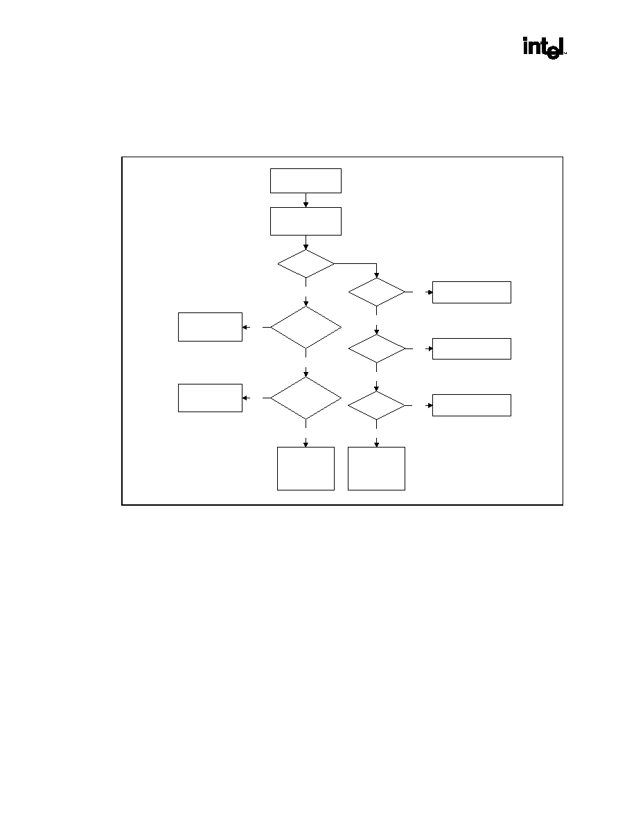
Intel
Æ
830 Chipset Family
60 Datasheet
298338-003
R
4.2.1
Intel 830 Chipset Family GMCH-M Configuration Cycle Flow
Charts
Figure 7. Configuration Cycle Flow Chart
DW I/O Write to
CONFIG_ADDRESS
with bit 31=1
I/O Read/Write to
CONFIG_DATA
BUS#=0
DEV#=0,
FN#=0
GMCH-M Claims Bus #0 /
Device #0 / Function #0
DEV#=1,
FN#=0
Yes
Yes
Yes
No
GMCH-M
Generates hub I/F
Type 1
Configuration
Cycle
BUS#=
SECONDARY BUS
in GMCH Dev #1
No
GMCH-M Generates
Type 0 Access to
AGP/PCI1
Yes
BUS# > SEC BUS
BUS# <= SUB BUS
No
GMCH-M Generates
Type 1 Access to
AGP/PCI1
Yes
No
GMCH-M
Generates hub I/F
Type 0
Configuration
Cycle
DEV#=2,
FN#=0/1
No
No
Yes
GMCH-M Claims Bus #0 /
Device #1 / Function #0
GMCH-M Claims Bus #0 /
Device #2 / Function #0/1
A detailed description of the mechanism for translating CPU I/O bus cycles to configuration cycles on
one of the two buses is described in Figure 7 above.
4.2.2
PCI Bus Configuration Mechanism
The PCI Bus defines a slot based "configuration space" that allows each device to contain up to 8
functions with each function containing up to 256, 8-bit configuration registers. The PCI specification
defines two bus cycles to access the PCI configuration space: Configuration Read and Configuration
Write. Memory and I/O spaces are supported directly by the CPU. Configuration space is supported by
a mapping mechanism implemented within the GMCH-M. The PCI specification defines two
mechanisms to access configuration space, Mechanism #1 and Mechanism #2. The GMCH-M supports
only Mechanism #1 for PCI configuration accesses.
The configuration access mechanism makes use of the CONFIG_ADDRESS Register and
CONFIG_DATA Register. To reference a configuration register, a Dword I/O write cycle is used to
place a value into CONFIG_ADDRESS that specifies the PCI bus, the device on that bus, the function
within the device, and a specific configuration register of the device function being accessed.
CONFIG_ADDRESS[31] must be first to enable a configuration cycle. CONFIG_DATA then becomes
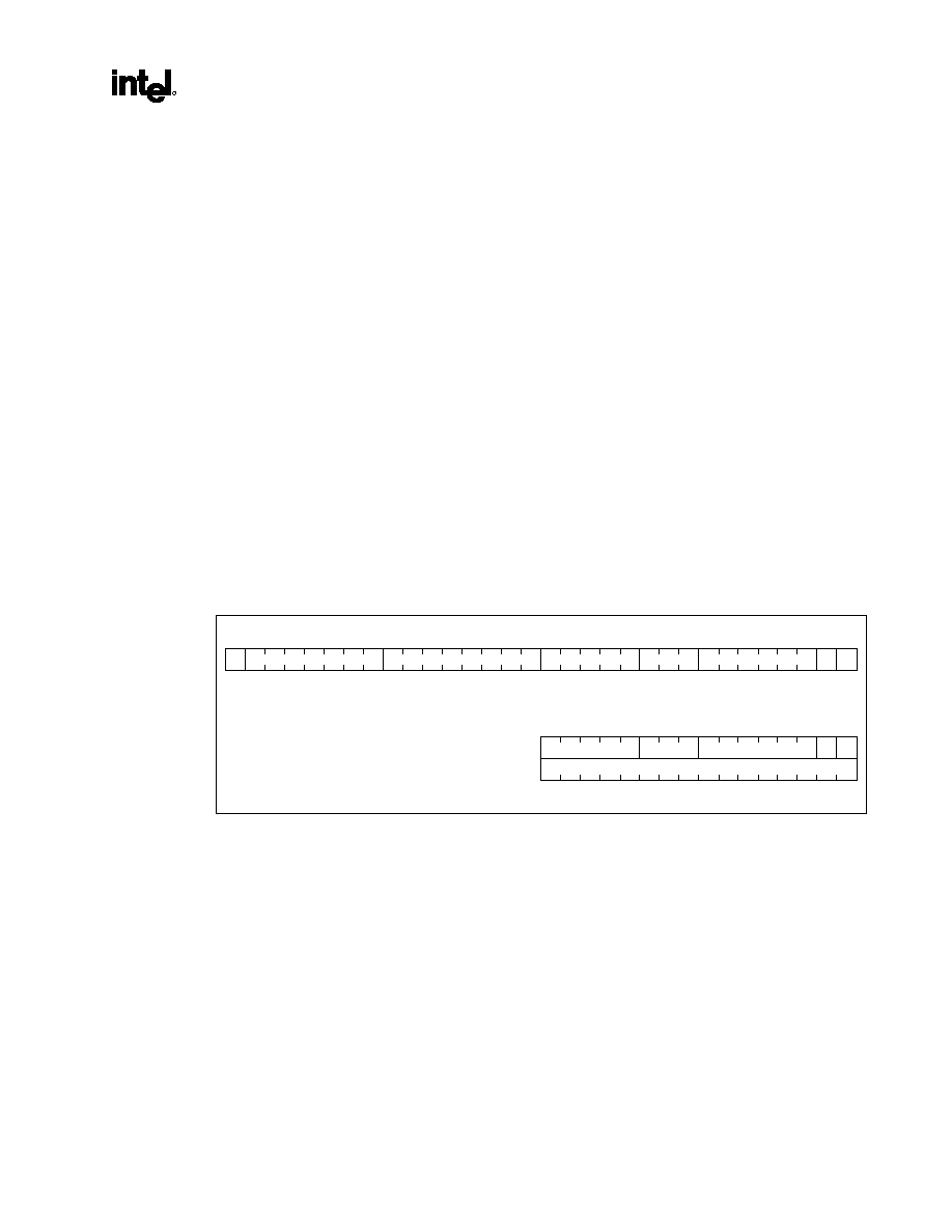
Intel
Æ
830 Chipset Family
298338-003 Datasheet
61
R
a window into the four bytes of configuration space specified by the contents of CONFIG_ADDRESS.
Any read or write to CONFIG_DATA will result in the Intel 830 Chipset family GMCH-M translating
the CONFIG_ADDRESS into the appropriate configuration cycle. The GMCH-M is responsible for
translating and routing the CPU's I/O accesses to the CONFIG_ADDRESS and CONFIG_DATA
registers to internal GMCH-M configuration registers, Hub Interface, or AGP/PCI1 (applicable when
discrete AGP is used with Intel 830M and 830MP Chipset).
4.2.3
PCI Bus #0 Configuration Mechanism
The Intel 830 Chipset family GMCH-M decodes the Bus Number (bits 23:16) and the Device Number
fields of the CONFIG_ADDRESS register. If the Bus Number field of CONFIG_ADDRESS is 0 the
configuration cycle is targeting a PCI Bus #0 device. The Host-Hub Interface Bridge entity within the
GMCH-M is hardwired as Device #0 on PCI Bus #0 (applicable to the entire 830 Chipset family). The
Host-AGP/PCI1 Bridge entity within the GMCH-M is hardwired as Device #1 on PCI Bus #0
(applicable only to the 830M and 830MP Chipset). The Integrated Graphics entity within the GMCH-M
is hardwired as Device #2 on PCI Bus#0 (applicable to 830M and 830MG Chipset). Configuration
cycles to any of the GMCH-M's internal devices are confined to the GMCH-M and not sent over Hub
Interface. Accesses to devices #3 to #31 will be forwarded over Hub Interface as Type 0 Configuration
Cycles (see Hub Interface spec). A[1:0] of the Hub Interface Request Packet for the Type 0
configuration cycle will be "00". Bits 15:2 of the CONFIG_ADDRESS register will be translated to the
A[15:2] field of the Hub Interface Request Packet of the configuration cycle as shown the figure below.
The ICH3-M decodes the Type 0 access and generates a configuration access to the selected internal
device.
Figure 8. Hub Interface Type 0 Configuration Address Translation
Device Number
Function No.
Register Number
0 0
Reserved
0
15
31
16
Type 0
x
x
Register Number
Function No.
Device Number
0
Reserved
1
CONFIG_ADDRESS
Hub Interface Type 0
Configuration
Address Extension
cfg_hl0.vsd
0
31
4.2.4
Primary PCI and Downstream Configuration Mechanism
If the Bus Number in the CONFIG_ADDRESS is non-zero, and is less than the value programmed into
the Intel 830 Chipset family GMCH-M's device #1 SECONDARY BUS NUMBER register or greater
than the value programmed into the SUBORDINATE BUS NUMBER Register, the GMCH-M will
generate a Type 1 Hub Interface Configuration Cycle. A[1:0] of the Hub Interface Request Packet for
the Type 1 configuration cycle will be "01". Bits 31:2 of the CONFIG_ADDRESS register will be
translated to the A[31:2] field of the Hub Interface Request Packet of the configuration cycle as shown
in the figure below. The ICH3-M compares the non-zero Bus Number with the SECONDARY BUS
NUMBER and SUBORDINATE BUS NUMBER registers of its P2P bridges to determine if the
configuration cycle is meant for Primary PCI, one of the ICH3-M's Hub Interfaces, or a downstream
PCI bus.
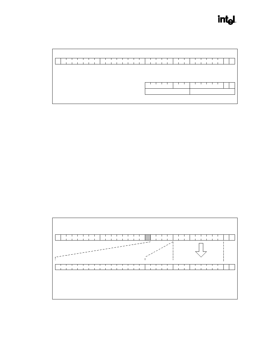
Intel
Æ
830 Chipset Family
62 Datasheet
298338-003
R
Figure 9. Hub Interface Type 1 Configuration Address Translation
Device Number
Function No.
Register Number
0 1
0
15
31
16
Type 1
x
x
Register Number
Function No.
Device Number
Bus Number
Reserved
1
CONFIG_ADDRESS
Hub Interface Type 1
Configuration
Address Extension
cfg_hl1.vsd
Reserved
Bus Number
31
0
4.2.5
Intel 830M and 830MP Chipset AGP/PCI1 Bus Configuration
Mechanism
From the chipset configuration perspective, AGP/PCI1 is seen as another PCI bus interface residing on a
Secondary Bus side of the "virtual" PCI-PCI bridge referred to as the Intel 830M and 830MP Chipset
GMCH-M Host-AGP/PCI1 bridge. On the Primary bus side, the "virtual" PCI-PCI Bridge is attached to
PCI Bus #0. Therefore, the PRIMARY BUS NUMBER register is hardwired to "0". The "virtual" PCI-
PCI bridge entity converts Type #1 PCI Bus Configuration cycles on PCI Bus #0 into Type 0 or Type 1
configuration cycles on the AGP/PCI1 interface. Type 1 configuration cycles on PCI Bus #0 that have a
BUS NUMBER that matches the SECONDARY BUS NUMBER of the GMCH-M's "virtual" PCI-PCI
Bridge will be translated into Type 0 configuration cycles on the AGP/PCI1 interface. The GMCH-M
will decode the Device Number field [15:11] and assert the appropriate GAD signal as an IDSEL in
accordance with the PCI-to-PCI Bridge Type 0 configuration mechanism. For PCI-to-PCI Bridge
translation one of 16 IDSELs are generated (as opposed to one of 21 for Host-to-PCI bridges).
When bit [15] = 0, bits [14:11] are decoded to assert a single AD[31:16] IDSEL. If bit [15] = 1,
AD[31:16] are 0000h. The remaining address bits will be mapped as described in Figure 10.
Figure 10. Mechanism #1 Type 0 Configuration Address to PCI Address Mapping
x
x
Register Number
Function No.
Device Number
Bus Number
Reserved
1
CONFIG_ADDRESS
AGP/PCI1 Type 0 Configuration Cycle
cfg_hl1.vsd
31
0
24 23
16 15
11 10
8
7
2
1
0
0
Register Number
Function No.
Reserved = 0
IDSEL
31
0
24 23
16 15
11 10
8
7
2
1
14
AGP GAD[31:0] Address
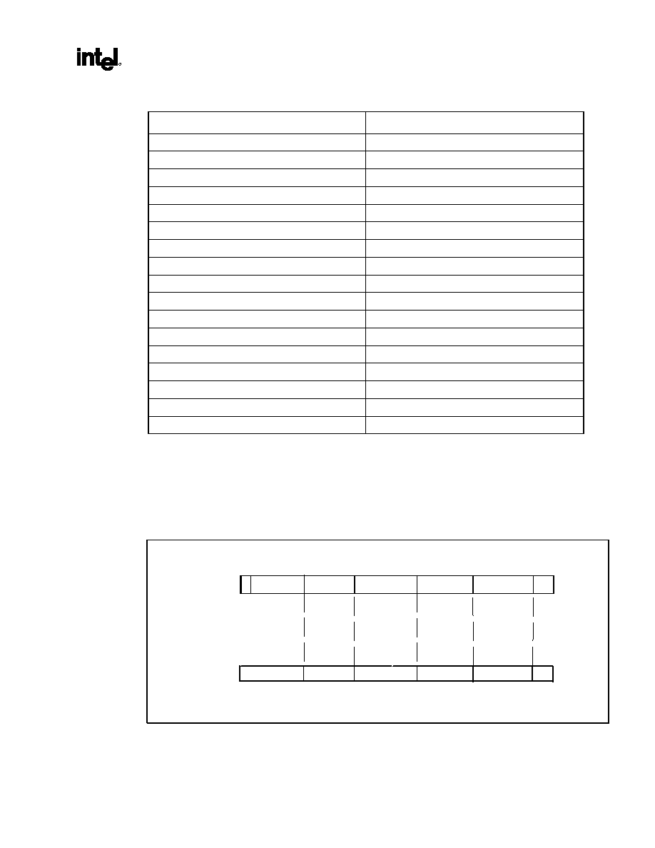
Intel
Æ
830 Chipset Family
298338-003 Datasheet
63
R
Table 23. AGP/PCI1 Config Address Remapping
Config Address AD[15:11]
AGP GAD[31:16] IDSEL
00000
0000 0000 0000 0001
00001
0000 0000 0000 0010
00010
0000 0000 0000 0100
00011
0000 0000 0000 1000
00100
0000 0000 0001 0000
00101
0000 0000 0010 0000
00110
0000 0000 0100 0000
00111
0000 0000 1000 0000
01000
0000 0001 0000 0000
01001
0000 0010 0000 0000
01010
0000 0100 0000 0000
01011
0000 1000 0000 0000
01100
0001 0000 0000 0000
01101
0010 0000 0000 0000
01110
0100 0000 0000 0000
01111
1000 0000 0000 0000
1xxxx
0000 0000 0000 0000
If the Bus Number is non-zero, greater than the value programmed into the SECONDARY BUS
NUMBER register and less than or equal to the value programmed into the SUBORDINATE BUS
NUMBER register, the configuration cycle is targeting a PCI bus downstream of AGP/PCI1. The 830M
and 830MP GMCH-M will generate a Type 1 PCI configuration cycle on AGP/PCI1. The address bits
will be mapped as described in figure below.
Figure 11. Mechanism #1 Type 1 Configuration Address to PCI Address Mapping
Reg. Index
Reg. Index
PCI Address
AD[31:0]
16 15
11
7
0
31
16 15
8 7
0
CONFIG_ADDRESS
X X
0
1
1
2
2 1
11 10
Device Number
Function Number
8
10
Bus Number
23
31 30
24
Reserved
1
Function Number
Device Number
Bus Number
23
24
0

Intel
Æ
830 Chipset Family
64 Datasheet
298338-003
R
To prepare for mapping of the configuration cycles on AGP/PCI1 the initialization software will go
through the following sequence:
1. Scan all devices residing on the PCI Bus #0 using Type 0 configuration accesses.
2. For every device residing at bus #0 which implements PCI-PCI bridge functionality, it will
configure the secondary bus of the bridge with the appropriate number and scan further down the
hierarchy. This process will include the configuration of the "virtual" PCI-PCI Bridge within the
830M and 830MP GMCH-M used to map the AGP address space in a software specific manner.
Note: Although initial AGP platform implementations will not support hierarchical buses residing below AGP,
this specification still must define this capability in order to support PCI-66 compatibility. Note also that
future implementations of the AGP devices may support hierarchical PCI or AGP-like buses coming out
of the root AGP device.
4.2.6
Intel 830 Chipset Family Internal GMCH-M Configuration
Register Access Mechanism
Accesses decoded as PCI Bus #0/Device #0 (Host-Hub Interface Bridge/SDRAM Controller), PCI Bus
#0/Device #1 (Host-AGP Bridge
1
), or PCI Bus #0/Device#2 (Integrated Graphics Device
1
) are
sequenced as Type 0 PCI Configuration Cycle accesses on Bus #0 to Device #0/Function #0, Device
#1/Function #0, and Device #2/Function #0/1. Note that since GMCH-M device #0 and #1 are not
multi-function devices, the function number should always be `0'. If the function number is not `0' for
accesses to Device #0 or #1, the GMCH-M will not claim the configuration cycle and it will be
forwarded to the Hub Interface where it should be master aborted (by the ICH3-M) in the same way as
transactions to other unimplemented PCI configuration targets.
Note: AGP is available only with the Intel 830MP and 830M Chipset. Internal graphics device is available
only with the Intel 830M and 830MG Chipset.
4.3
Intel 830 Chipset Family GMCH-M Register Introduction
The Intel 830 Chipset family GMCH-M contains two sets of software accessible registers, accessed via
the Host CPU I/O address space:
1. Control registers I/O mapped into the CPU I/O space, which control access to PCI and AGP
configuration space (see section entitled I/O Mapped Registers).
2. Internal configuration registers residing within the GMCH-M that are partitioned into three logical
device register sets ("logical" since they reside within a single physical device). The first register
set is dedicated to Host-Hub Interface Bridge functionality (controls PCI Bus #0 i.e. SDRAM
configuration, other chip-set operating parameters and optional features). The second register
block is dedicated to Host-AGP/PCI1 Bridge functions (controls AGP/PCI1 interface
configurations and operating parameters). The third register block is dedicated to the Integrated
Graphics Device (IGD) function.
Note: AGP is only available with 830M and 830MP Chipset; internal graphics device is available with 830M
and 830MG Chipset
Note: This configuration scheme is necessary to accommodate the existing and future software configuration
model supported by Microsoft* where the Host Bridge functionality will be supported and controlled via
a dedicated specific driver. Virtual PCI-PCI Bridge functionality will be supported via standard PCI bus
enumeration configuration software. The term "virtual" is used to designate that no real physical
embodiment of the PCI-PCI Bridge functionality exists within the GMCH-M, but that GMCH-M's

Intel
Æ
830 Chipset Family
298338-003 Datasheet
65
R
internal configuration register sets are organized in this particular manner to create that impression to the
standard configuration software.
The GMCH-M supports PCI configuration space accesses using the mechanism denoted as
Configuration Mechanism #1 in the PCI specification. The GMCH-M internal registers (both I/O
Mapped and Configuration registers) are accessible by the Host CPU. The registers can be accessed as
Byte, Word (16-bit), or Dword (32-bit) quantities, with the exception of CONFIG_ADDRESS that can
only be accessed as a Dword. All multi-byte numeric fields use "little-endian" ordering (i.e., lower
addresses contain the least significant parts of the field).
Some of the GMCH-M registers described in this section contain reserved bits. These bits are labeled
"Reserved". Software must deal correctly with fields that are reserved. On reads, software must use
appropriate masks to extract the defined bits and not rely on reserved bits being any particular value. On
writes, software must ensure that the values of reserved bit positions are preserved. That is, the values of
reserved bit positions must first be read, merged with the new values for other bit positions and then
written back. Note the software does not need to perform read, merge, and write operations for the
configuration address register.
In addition to reserved bits within a register, the GMCH-M contains address locations in the
configuration space of the Host-Hub Interface Bridge entity that are marked either "Reserved" or "Intel
Reserved". The GMCH-M responds to accesses to "Reserved" address locations by completing the host
cycle. When a "Reserved" register location is read, a zero value is returned. ("Reserved" registers can be
8-, 16-, or 32-bit in size). Writes to "Reserved" registers have no effect on the GMCH-M. Registers that
are marked as "Intel Reserved" must not be modified by system software. Writes to "Intel Reserved"
registers may cause system failure. Reads to "Intel Reserved" registers may return a non-zero value.
Upon Reset, the GMCH-M sets all of its internal configuration registers to predetermined default states.
Some register values at reset are determined by external strapping options. The default state represents
the minimum functionality feature set required to successfully bring up the system. Hence, it does not
represent the optimal system configuration. It is the responsibility of the system initialization software
(usually BIOS) to properly determine the SDRAM configurations, operating parameters and optional
system features that are applicable, and to program the GMCH-M registers accordingly.
4.4
Intel 830 Chipset Family I/O Mapped Registers
The Intel 830 Chipset family GMCH-M contains a set of registers that reside in the CPU I/O address
space - the Configuration Address (CONFIG_ADDRESS) Register and the Configuration Data
(CONFIG_DATA) Register. The Configuration Address Register enables/disables the configuration
space and determines what portion of configuration space is visible through the Configuration Data
window.
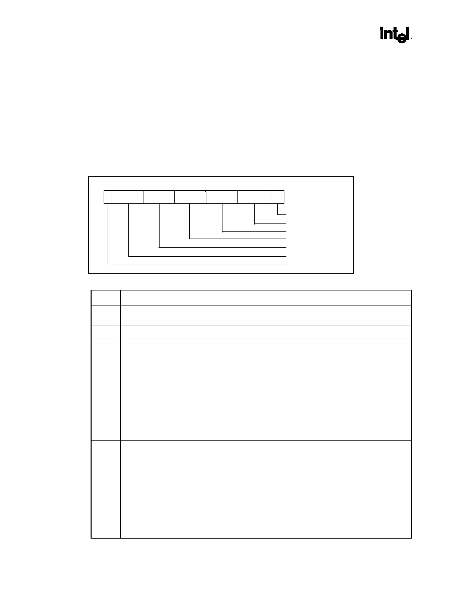
Intel
Æ
830 Chipset Family
66 Datasheet
298338-003
R
4.4.1
CONFIG_ADDRESS - Configuration Address Register
I/O Address:
0CF8h Accessed as a Dword
Default Value:
00000000h
Access:
Read/Write
Size:
32
bits
CONFIG_ADDRESS is a 32-bit register accessed only when referenced as a Dword. A Byte or Word
reference will "pass through" the Configuration Address Register and Hub Interface onto the PCI0 bus
as an I/O cycle. The CONFIG_ADDRESS register contains the Bus Number, Device Number, Function
Number, and Register Number for which a subsequent configuration access is intended.
R
1 0
2
7
8
11
15
16
23
24
30
3
1
10
R 0 0 0 0
0
Reserved
Register Number
Function Number
Device Number
Bus Number
Reserved
Enable
Bit
Default
Bit Descriptions
31
Configuration Enable (CFGE). When this bit is set to 1, accesses to PCI configuration space are
enabled. If this bit is reset to 0, accesses to PCI configuration space are disabled.
30:24
Reserved (These bits are read only and have a value of 0).
23:16
Bus Number. When the Bus Number is programmed to 00h the target of the Configuration Cycle is
either the GMCH-M or the ICH3-M. The Configuration Cycle is forwarded to hub interface if the Bus
Number is programmed to 00h and no device internal to the GMCH-M is the target.
If the Bus Number is non-zero and matches the value programmed into the SECONDARY BUS
NUMBER Register of the AGP/PCI1 bridge, a Type 0 PCI configuration cycle will be generated on
AGP/PCI1.
If the Bus Number is non-zero, greater than the value in the SECONDARY BUS NUMBER register of the
AGP/PCI1 bridge, and less than or equal to the value programmed into the SUBORDINATE BUS
NUMBER Register, a Type 1 PCI configuration cycle will be generated on AGP/PCI1.
If the Bus Number is non-zero, and is less than the value programmed into the SECONDARY BUS
NUMBER Register of the AGP/PCI1 bridge, or is greater than the value programmed into the
SUBORDINATE BUS NUMBER Register, a Type 1 hub interface Configuration Cycle is generated.
15:11
Device Number. This field selects one agent on the PCI bus selected by the Bus Number. When the Bus
Number field is "00" the GMCH-M decodes the Device Number field. The GMCH-M is always Device #0
for the Host-hub interface bridge entity, Device #1 for the Host-AGP/PCI1 entity, and Device #2 for the
Integrated Graphics Device entity. Therefore, when the Bus Number = 0 and the Device Number = 0, 1,
or 2, the internal GMCH-M devices are selected.
If the Bus Number is non-zero and matches the value programmed into the SECONDARY BUS
NUMBER Register of the AGP/PCI1 bridge, a Type 0 PCI configuration cycle will be generated on
AGP/PCI1. The Device Number field is decoded and the GMCH-M asserts one and only one GADxx
signal as an IDSEL. GAD11 is asserted to access Device #0, GAD12 for Device #1, and so forth up to
Device #20 for which will assert GAD31. All device numbers higher than 20 cause a type 0 configuration
access with no IDSEL asserted, which will result in a Master Abort reported in the GMCH-M's "virtual"
PCI-PCI bridge registers.
Intel
Æ
830 Chipset Family
298338-003 Datasheet
67
R
For Bus Numbers resulting in AGP/PCI1 Type 1 Configuration cycles, the Device Number is propagated
as GAD[15:11].
10:8
Function Number. This field is mapped to GAD[10:8] during AGP/PCI1 Configuration cycles. This allows
the configuration registers of a particular function in a multi-function device to be accessed. The GMCH-
M ignores configuration cycles to Devices 1 if the function number is not equal to 0.
7:2
Register Number. This field selects one register within a particular Bus, Device, and Function as
specified by the other fields in the Configuration Address Register. This field is mapped to GAD[7:2]
during AGP/PCI1 Configuration cycles.
1:0
Reserved
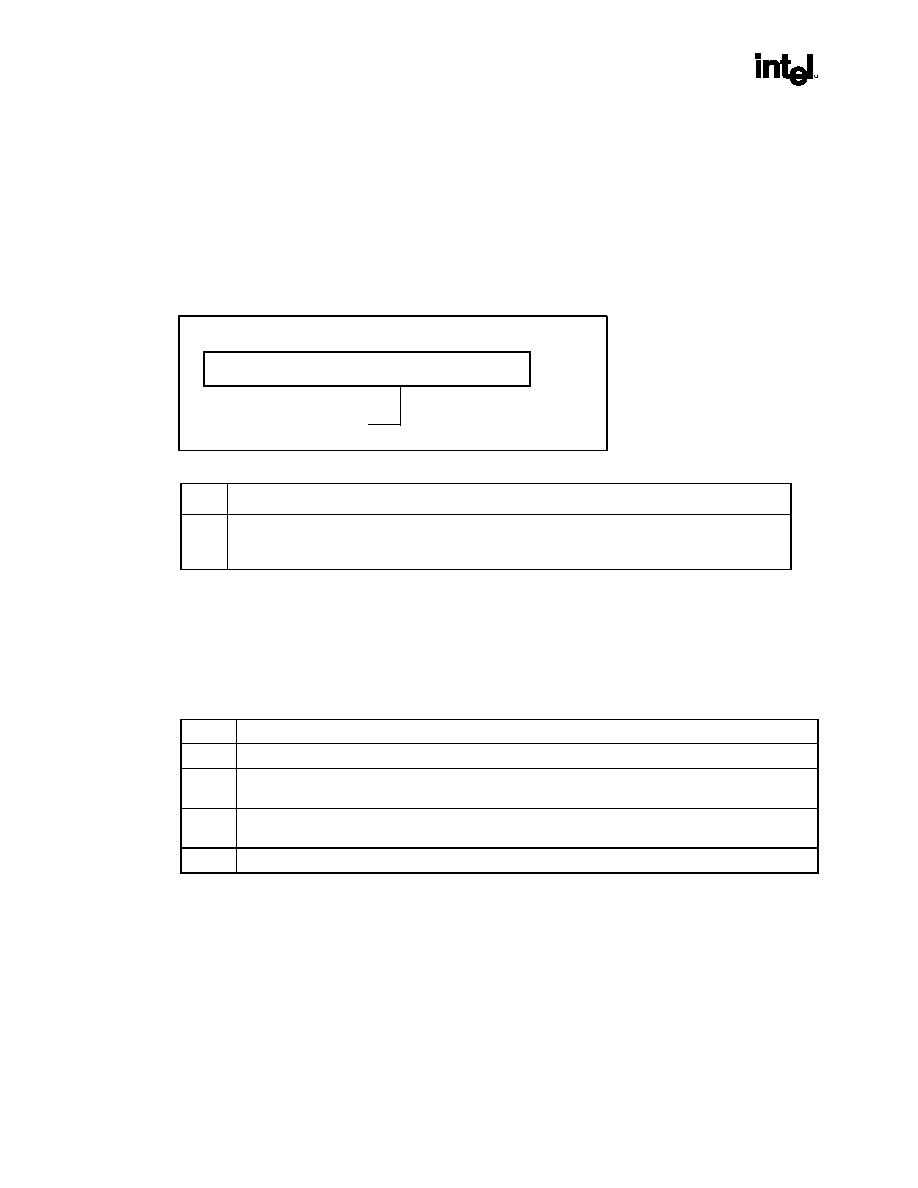
Intel
Æ
830 Chipset Family
68 Datasheet
298338-003
R
4.4.2
CONFIG_DATA - Configuration Data Register
I/O Address:
0CFCh
Default Value:
00000000h
Access:
Read/Write
Size:
32
bits
CONFIG_DATA is a 32-bit read/write window into configuration space. The portion of configuration
space that is referenced by CONFIG_DATA is determined by the contents of CONFIG_ADDRESS.
31
0
Bit
Default
0
Configuration Data Window
Bit Descriptions
31:0
Configuration Data Window (CDW). If bit 31 of CONFIG_ADDRESS is 1, any I/O access to the
CONFIG_DATA register will be mapped to configuration space using the contents of
CONFIG_ADDRESS.
4.5
Intel 830 Chipset Family GMCH-M Internal Device
Registers
Table 24 below shows the nomenclature of access attributes for the configuration space of each device.
Table 24. Nomenclature for Access Attributes
RO Read
Only. If a register is read only, writes to this register have no effect.
R/W Read/Write. A register with this attribute can be read and written
R/WC Read/Write
Clear. A register bit with this attribute can be read and written. However, a write of a 1 clears
(sets to 0) the corresponding bit and a write of a 0 has no effect.
R/WO Read/Write
Once. A register bit with this attribute can be written to only once after power up. After the
first write, the bit becomes read only.
L Lock. A register bit with this attribute becomes Read Only after a lock bit is set.

Intel
Æ
830 Chipset Family
298338-003 Datasheet
69
R
4.5.1
SDRAM Controller/Host-hub Interface Device Registers -
Device #0
Table 25 shows the GMCH-M configuration space for device #0 (applicable to the entire 830 Chipset
family). An "s" in the Default Value field means that a strap determines the power-up default value for
that bit.
Table 25. Host-Hub I/F Bridge/SDRAM Controller Configuration Space (Device #0)
Address
Offset
Register
Symbol
Register Name
Default Value
Access
00-01h VID Vendor
Identification
8086h
RO
02-03h DID Device
Identification
3575h
RO
04-05h
PCICMD
PCI Command Register
0006h
R/W
06-07h
PCISTS
PCI Status Register
0010h
RO, R/WC
08h RID
Revision
Identification
00h
RO
09h - Intel
Reserved
-
-
0Ah SUBC
Sub-Class
Code
00h
RO
0Bh
BCC
Base Class Code
06h
RO
0Ch - Intel
Reserved
-
-
0Dh MLT
Master
Latency
Timer
00h
RO
0Eh HDR
Header
Type
00h
RO
0Fh - Intel
Reserved
-
-
10-13h
APBASE
Aperture Base Configuration
00000008h
R/W, RO
14-2Bh -
Intel
Reserved
-
-
2C-2Dh SVID Subsystem
Vendor
Identification 00h
R/WO
2E-2Fh SID Subsystem
Identification
00h
R/WO
30-33h -
Intel
Reserved
-
-
34h CAPPTR
Capabilities
Pointer
40h
RO
35-3Fh -
Intel
Reserved
-
-
40-44h
-
Intel Reserved
-
-
45-47h
-
Intel Reserved
-
-
48-4Bh
RRBAR
Register Range Base Address
00000000h
R/W, RO
4C-4Fh
-
Intel Reserved
-
-
50-51h
GCC0
GMCH Control Register 0
A072h
R/W, RO
52-53h
GCC1
GMCH Control Register 1
0000h
R/W
54-55h
-
Intel Reserved
-
-
56-57h
-
Intel Reserved
-
-
58h
FDHC
Fixed DRAM Hole Control
00h
R/W
59-5Fh
PAM[6:0]
Programmable Attribute Map (7
i
)
00h
R/W

Intel
Æ
830 Chipset Family
70 Datasheet
298338-003
R
registers)
60-67h
DRB[7:0]
DRAM Row Boundary Register
00h
R/W/L
68-6Fh
-
Intel Reserved
-
-
70-71h
DRA[1:0]
DRAM Row Attributes
FFh
R/W/L
72-77h
-
Intel Reserved
-
-
78-7Bh
DRT
DRAM Timing Register
00000010h
R/W
7C-7Fh
DRC
DRAM Control
00000000h
R/W
80-8Bh
-
Intel Reserved
-
-
8C-8Fh
DTC
DRAM Throttling Control Register
00000000h
R/W/L
90h
SMRAM
System Management RAM Control Reg.
02h
R/W/L
91h
ESMRAMC
Extended System Management RAM
Control Register
38h R/W
92-93h ERRSTS
Error
Status
Register
0000h
R/W
94-95h
ERRCMD
Error Command Register
0000h
R/W
96h - Intel
Reserved
-
-
97h - Intel
Reserved
-
-
98-9F -
Intel
Reserved
-
-
A0-A3h ACAPID
AGP
Capability
Identifier
00200002h RO*
A4-A7h
AGPSTAT
AGP Status Register
1F000217h
RO*
A8-ABh
AGPCMD
AGP Command Register
00000000h
RW*
AC-AFh -
Intel
Reserved
-
-
B0-B1h
AGPCTRL
AGP Control Register
0000h
R/W*
B2-B3h
AFT
AGP Functional Test Register
0000h
R/W*
B4h APSIZE
AGP
Aperture
Size
00h
R/W*
B5-B7h -
Intel
Reserved
-
-
B8-BBh ATTBASE
Aperture
Translation
Table
00000000h R/W*
BCh
AMTT
AGP Interface Multi-Transaction Timer
Register
00h R/W*
BDh
LPTT
Low Priority Transaction Timer Register
00h
R/W*
BE-BFh -
Intel
Reserved
-
-
C2-EBh -
Intel
Reserved
-
-
EC-EFh
BUFF_SC
System Memory Buffer Strength Control
Register
00000000h R/W
F0-FFh -
Intel
Reserved
-
-
NOTE: *Register is READ ONLY (RO) when internal graphics device is used with the Intel 830MG Chipset is used.
Register will have no functionality when internal graphics device is used with Intel 830M Chipset.
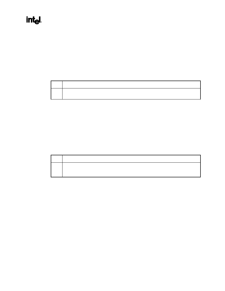
Intel
Æ
830 Chipset Family
298338-003 Datasheet
71
R
4.5.1.1
VID - Vendor Identification Register - Device #0
Address Offset:
00 - 01h
Default Value:
8086h
Attribute:
Read Only
Size:
16
bits
The VID Register contains the vendor identification number. This 16-bit register combined with the
Device Identification Register uniquely identifies any PCI device. Writes to this register have no effect.
Bit Description
15:0
Vendor Identification Number. This is a 16-bit value assigned to Intel. Intel VID = 8086h.
Default Value=1000/0000/1000/0110.
4.5.1.2
DID - Device Identification Register - Device #0
Address Offset:
02 - 03h
Default Value:
3575h
Attribute:
Read Only
Size:
16
bits
This 16-bit register combined with the Vendor Identification register uniquely identifies any PCI device.
Writes to this register have no effect.
Bit Description
15:0
Device Identification Number. This is a 16-bit value assigned to the GMCH-M Host-hub interface
Bridge, Device #0.
Default Value=0011/0101/0111/0101.

Intel
Æ
830 Chipset Family
72 Datasheet
298338-003
R
4.5.1.3
PCICMD - PCI Command Register - Device #0
Address Offset:
04-05h
Default Value:
0006h
Access:
Read/Write
Size
16
bits
Since GMCH-M Device #0 is the host-to-Hub Interface bridge, many of the PCI specific bits in this
register don't apply.
Bit Description
15:10
Reserved
9
Fast Back-to-Back. This bit controls whether or not the master can do fast back-to-back write. Since
device #0 is strictly a target this bit is not implemented and is hardwired to 0. Writes to this bit position
have no effect.
Default Value=0.
8
SERR Enable (SERRE). This bit is a global enable bit for Device #0 SERR messaging. The GMCH-M
does not have an SERR# signal. The GMCH-M communicates the SERR# condition by sending an SERR
message to the ICH3-M. If this bit is set to a 1, the GMCH-M is enabled to generate SERR messages over
Hub Interface for specific Device #0 error conditions that are individually enabled in the ERRCMD register.
The error status is reported in the ERRSTS and PCISTS registers. If SERRE is reset to 0, then the SERR
message is not generated by the GMCH-M for Device #0.
NOTE: This bit only controls SERR messaging for the Device #0. Device #1 has its own SERRE bit to
control error reporting for error conditions occurring on Device #1. The two control bits are used in a
logical OR manner to enable the SERR Hub Interface message mechanism.
Default Value=0.
7
Address/Data Stepping. Address/data stepping is not implemented in the GMCH-M, and this bit is
hardwired to 0. Writes to this bit position have no effect.
Default Value=0.
6
Parity Error Enable (PERRE). PERR# is not implemented by the GMCH-M, and this bit is hardwired to 0.
Writes to this bit position have no effect.
Default Value=0.
5
VGA Palette Snoop. The GMCH-M does not implement this bit and it is hardwired to a 0. Writes to this bit
position have no effect.
Default Value=0.
4
Memory Write and Invalidate Enable. The GMCH-M will never use this command and this bit is
hardwired to 0. Writes to this bit position have no effect.
Default Value=0.
3
Special Cycle Enable. The GMCH-M does not implement this bit and it is hardwired to a 0. Writes to this
bit position have no effect.
Default Value=0.
2
Bus Master Enable (BME). The GMCH-M is always enabled as a master on Hub Interface. This bit is
hardwired to a 1. Writes to this bit position have no effect.
Default Value=1.
1
Memory Access Enable (MAE). The GMCH-M always allows access to main memory. This bit is not
implemented and is hardwired to 1. Writes to this bit position have no effect.
Default Value=1.
0
I/O Access Enable (IOAE). This bit is not implemented in the GMCH-M and is hardwired to a 0. Writes to
this bit position have no effect.
Default Value=0.

Intel
Æ
830 Chipset Family
298338-003 Datasheet
73
R
4.5.1.4
PCISTS - PCI Status Register - Device #0
Address Offset:
06-07h
Default Value:
0010h
Access:
Read Only, Read/Write Clear
Size:
16
bits
PCISTS is a 16-bit status register that reports the occurrence of error events on Device #0's Hub
Interface. Bit 14 is read/write clear. All other bits are Read Only. Since GMCH-M Device #0 is the
host-to-Hub Interface bridge, many of the PCI specific bits in this register do not apply.
Bit Description
15
Detected Parity Error (DPE). This bit is hardwired to a 0. Writes to this bit position have no effect.
Default Value=0.
14
Signaled System Error (SSE). This bit is set to 1 when GMCH-M Device #0 generates an SERR
message over Hub Interface for any enabled Device #0 error condition. Device #0 error conditions are
enabled in the PCICMD and ERRCMD registers. Device #0 error flags are read/reset from the PCISTS
or ERRSTS registers. Software sets SSE to 0 by writing a 1 to this bit.
Default Value=0.
13
Received Master Abort Status (RMAS). This bit is set when the GMCH-M generates a Hub
Interface request that receives a Master Abort completion packet. Software clears this bit by writing a
1 to it.
Default Value=0.
12
Received Target Abort Status (RTAS). This bit is set when the GMCH-M generates a Hub Interface
request that receives a Target Abort completion packet. Software clears this bit by writing a 1 to it.
Default Value=0.
11
Signaled Target Abort Status (STAS). The GMCH-M will not generate a Target Abort Hub Interface
completion packet. This bit is not implemented in the GMCH-M and is hardwired to a 0. Writes to this
bit position have no effect.
Default Value=0.
10:9
DEVSEL# Timing (DEVT). Hub Interface does not comprehend DEVSEL# protocol. These bits are
hardwired to "00". Writes to these bits have no effect.
Default Value=00.
8
Data Parity Detected (DPD). GMCH-M does not support parity on Hub Interface. This bit is hardwired
to a 0. Writes to this bit position have no effect.
Default Value=0.
7
Fast Back-to-Back (FB2B). Hub Interface does not comprehend PCI Fast Back-to-Back protocol.
This bit is hardwired to 0. Writes to this bit position have no effect.
Default Value=0.
6:5
Reserved
4
Capability List (CLIST). This bit is hardwired to 1 to indicate to the configuration software that this
device/function implements a list of new capabilities.
A list of new capabilities is accessed via register CAPPTR at configuration address offset 34h.
Register CAPPTR contains an offset pointing to the start address within configuration space of this
device where the Capabilities linked list begins.
Default Value=1.
3:0
Reserved

Intel
Æ
830 Chipset Family
74 Datasheet
298338-003
R
4.5.1.5
RID - Revision Identification Register - Device #0
Address Offset:
08h
Default Value:
03h (A5 silicon)
04h
(A6
silicon)
Access:
Read
Only
Size:
8
bits
This register contains the revision number of the GMCH-M Device #0. These bits are read only and
writes to this register have no effect.
Bit Description
7:0
Revision Identification Number. This is an 8-bit value that indicates the revision identification number for
the GMCH-M Device #0. Please see spec update for the latest silicon revision.
Silicon Revision Default Value
A5 0000/0011 (03h)
A6 0000/0100 (04h)
4.5.1.6
SUBC - Sub-Class Code Register - Device #0
Address Offset:
0Ah
Default Value:
00h
Access:
Read
Only
Size:
8
bits
This register contains the Sub-Class Code for the GMCH-M Device #0. This code is 00h indicating a
Host Bridge device. The register is read only.
Bit Description
7:0
Sub-Class Code (SUBC). This is an 8-bit value that indicates the category of Bridge into which the GMCH-
M falls. The code is 00h indicating a Host Bridge.
Default Value=0000/0000.
Intel
Æ
830 Chipset Family
298338-003 Datasheet
75
R
4.5.1.7
BCC - Base Class Code Register - Device #0
Address Offset:
0Bh
Default Value:
06h
Access:
Read
Only
Size:
8
bits
This register contains the Base Class Code of the GMCH-M Device #0. This code is 06h indicating a
Bridge device. This register is read only.
Bit Description
7:0
Base Class Code (BASEC). This is an 8-bit value that indicates the Base Class Code for the GMCH-M. This
code has the value 06h.
Default Value=0000/0110.
4.5.1.8
MLT - Master Latency Timer Register - Device #0
Address Offset:
0Dh
Default Value:
00h
Access:
Read
Only
Size:
8
bits
Hub Interface does not comprehend the concept of a Master Latency Timer. Therefore the functionality
of this register is not implemented and the register is hardwired to 0.
Bit Description
7:0
These bits are hardwired to 0. Writes have no effect.
Default Value=0000/0000.
4.5.1.9
HDR - Header Type Register - Device #0
Address Offset:
0Eh
Default Value:
00h
Access:
Read
Only
Size:
8
bits
This register identifies the header layout of the configuration space. No physical register exists at this
location.
Bit Descriptions
7:0
This read only field always returns 0 when read and writes have no effect.
Default Value=0000/0000.

Intel
Æ
830 Chipset Family
76 Datasheet
298338-003
R
4.5.1.10
APBASE - Aperture Base Configuration Register - Device #0
Address Offset:
10-13h
Default Value:
00000008h
Access:
Read/Write, Read Only
Size:
32
bits
The APBASE is a standard PCI Base Address register that is used to set the base of the Graphics
Aperture. The standard PCI Configuration mechanism defines the base address configuration register
such that only a fixed amount of space can be requested (dependent on which bits are hardwired to "0"
or behave as hardwired to "0").
To allow for flexibility (of the aperture) an additional register called APSIZE is used as a "back-end"
register to control which bits of the APBASE will behave as hardwired to "0". This register will be
programmed by the GMCH-M specific BIOS code that will run before any of the generic configuration
software is run.
Note that bit 9 of the GCC0 register at 51-50h is used to prevent accesses to the aperture range before the
configuration software initializes this register and the appropriate translation table structure has been
established in the main memory.
Bit Description
31:28
Upper Programmable Base Address bits (R/W). These bits are used to locate the range size selected
via lower bits 27:4.
Default Value = 0000.
27:25
Lower "Hardwired"/Programmable Base Address bits. These bits behave as a "hardwired" or as a
programmable depending on the contents of the APSIZE register as defined below:
27 26 25 Aperture Sizer/w
r/w r/w r/w 32 MB
r/w r/w r/w 64 MB
r/w 0 0 128 MB
0 0 0 256 MB
The Default for APSIZE[5:3,0]=0000 with forces default APBASE[27:25] =000 (i.e. all bits respond as
"hardwired" to 0). This provides a default to the maximum aperture size of 256MB. The GMCH-M specific
BIOS is responsible for selecting smaller size (if required) before PCI configuration software runs and
establishes the system address map.
Default Value=000.
24:4
Hardwired to "0". This forces minimum aperture size selected by this register to be 32 MB.
3
Prefetchable (RO). This bit is hardwired to "1" to identify the Graphics Aperture range as a prefetchable,
i.e. there are no side effects on reads, the device returns all bytes on reads regardless of the byte enables,
and the GMCH-M may merge processor writes into this range without causing errors.
2:1
Type (RO). These bits determine addressing type and they are hardwired to "00" to indicate that address
range defined by the upper bits of this register can be located anywhere in the 32-bit address space.
Default Value=00.
0
Memory Space Indicator (RO). Hardwired to "0" to identify aperture range as a memory range.
Intel
Æ
830 Chipset Family
298338-003 Datasheet
77
R
4.5.1.11
SVID - Subsystem Vendor ID - Device #0
Address Offset:
2C-2Dh
Default Value:
0000h
Access:
Read/Write
Once
Size:
16
bits
This value is used to identify the vendor of the subsystem.
Bit Description
15:0
Subsystem Vendor ID (R/WO). The default value is 00h. This field should be programmed during boot-up.
After this field is written once, it becomes read only.
Default Value=0000/0000/0000/0000.
4.5.1.12
SID - Subsystem ID - Device #0
Address Offset:
2E-2Fh
Default Value:
0000h
Access:
Read/Write
Once
Size:
16
bits
This value is used to identify a particular subsystem.
Bit Description
15:0
Subsystem ID (R/WO). The default value is 00h. This field should be programmed during boot-up.
After this field is written once, it becomes read only.
Default Value=0000/0000/0000/0000.
4.5.1.13
CAPPTR - Capabilities Pointer - Device #0
Address Offset:
34h
Default Value:
40h
Access:
Read
Only
Size:
8
bits
The CAPPTR provides the offset that is the pointer to the location where the first capability register set
is located.
Bit Description
7:0
Pointer to the start of Capabilities Register Block. The value in this field is 40h.
Default Value=0100/0000.
Intel
Æ
830 Chipset Family
78 Datasheet
298338-003
R
4.5.1.14
RRBAR - Register Range Base Address Register - Device #0
Address Offset:
48-4Bh
Default Value:
00000000h
Access:
Read/Write, Read Only
Size:
32
bits
This register requests a 256-KB allocation for the Device registers. The base address is defined by bits
31 to 18 and can be used to access device configuration registers. Only Dword aligned writes are
allowed to this space. See Table below for address map within the 512-KB space.
This addressing mechanism may be used to write to registers that modify the device address map
(includes all the BARs, PAMs, SMM registers, Pre-Allocated Memory registers etc). However, before
using or allowing the use of the modified address map the BIOS must synchronize using an IO or Read
cycle.
Note that bit 8 of the GCC0 register at 51-50h is used to prevent accesses to this range before the
configuration software initializes this register.
Bit Description
31:18
Memory Base Address-R/W. Set by the OS, these bits correspond to address signals [31:18].
Default Value=0000/0000/0000/0.
17:15
Address Mask-RO. Hardwired to 0s to indicate 512-KB address range. The Minimum size that can be
requested by converting all these bits to R/W would be 64 KB.
Default Value=000.
15:8
Reserved. Hardwired to 00h.
7:0
Scratch Pad Size-RO, Hardwired to "00h".
00h = 256B
FFh = 64 KB
Default Value=0000/0000.
Address Range
Sub Ranges
Description
00000h to 0003Fh
Read Only: Maps to 00-3Fh of Device #0 P&P register space.
00040h to 000FFh
Read/Write: Maps to 40-FFh of Device #0 P&P register space.
00100h to 3FEFFh
Read/Write: Extended Register Space. Reserved.
00000h to
3FFFFhDevice 0
Space
3FF00h to 3FFFFh
Scratch Pad Registers: 256 B, D-word read/write-able.

Intel
Æ
830 Chipset Family
298338-003 Datasheet
79
R
4.5.1.15
GCC0 - GMCH Control Register #0 - Device #0
Address Offset:
50-51h
Default Value:
A072h
Access:
Read/Write, Read Only
Size:
16
bits
Bit Descriptions
15
Reserved
14:12
Low Priority Grace Period. This value is loaded in SDRAM Arbiter when a request is ongoing and a
higher priority request is presented to the Arbiter. The arbiter continues to grant the first request for this
specified number of page hits (1 KB). If the first requester causes a page miss or stops requesting the
arbiter will switch to the higher priority requester. (A request equals an Oct-word also known as dual-oct
byte).
000 = 00
001 = 04
010 = 08 (Default)
011 = 16
100 = 24
101 = 32
110 = Reserved
111 = Reserved
Default Value=010.
Recommended Value with Internal Graphics = 010
8
Recommended Value without Internal Graphics = 011
16
11
Scratch Pad Enable. This bit when set to a "1", allows the upper 256 Bytes of Device #0 RRBAR space
to be mapped to Scratch Pad Ram in the device. Once D_LCK is set, this bit becomes read only.
NOTE: The BIOS can use the scratch pad area when devices on the AGP bus are inactive (Not capable of
using the AGP Pipe or Side-Band command bus to issue read cycles to Main Memory).
Default Value=0.
10
Reserved.
9
Aperture Access Global Enable (R/W). This bit is used to prevent access to the aperture from any port
(CPU, PCI0 or AGP/PCI1) before the aperture range is established by the configuration software and
appropriate translation table in the main SDRAM has been initialized. It must be set after system is fully
configured for aperture accesses.
Default Value=0.
8
RRBAR Access Enable. This bit when set to a "1", enables the RRBAR space. When "0", accesses will
not decode to register range.
Default Value=0.
7
Reserved
6:4
IOQ request Grant Ceiling. This value is loaded in SDRAM Arbiter when an IOQ request is granted. It
provides a grant for the duration specified for as long as the request is active or until a fixed higher priority
request needs to be serviced.
111 = Infinite Ceiling (Default)
110 = 64
101 = 48
100 = 32
011 = 24

Intel
Æ
830 Chipset Family
80 Datasheet
298338-003
R
010 = 16
001 = 08
000 = 04
Default Value=111.
Please contact your Intel Field Representative for more information.
3:1
Reserved
0
MDA Present (MDAP) (R/W).
This bit works with the VGA Enable bit in the BCTRL register of device 1 to control the routing of CPU
initiated transactions targeting MDA compatible I/O and memory address ranges. This bit should not be
set when the VGA Enable bit is not set.
If the VGA enable bit is set, then accesses to IO address range x3BCh-x3BFh are forwarded to Hub
Interface.
If the VGA enable bit is not set then accesses to IO address range x3BCh-x3BFh are treated just like any
other IO accesses i.e. the cycles are forwarded to AGP if the address is within IOBASE and IOLIMIT and
ISA enable bit is not set, otherwise they are forwarded to Hub Interface. MDA resources are defined as the
following:
Memory: 0B0000h - 0B7FFFhI/O:
I/O: 3B4h, 3B5h, 3B8h, 3B9h, 3BAh, 3BFh, (including ISA address aliases, A[15:10] are not used in
decode)
Any I/O reference that includes the I/O locations listed above, or their aliases, will be forwarded to Hub
Interface even if the reference includes I/O locations not listed above. The following table shows the
behavior for all combinations of MDA and VGA:
VGA MDA Behavior
Default 0 0 All References to MDA and VGA go to Hub Interface
0 1 Illegal Combination (DO NOT USE)
1 0 All References to VGA go to AGP/PCI.
MDA-only references (I/O address 3BF and aliases) will go to Hub Interface.
1 1 VGA References go to AGP/PCI; MDA References go to Hub Interface
Default Value=0.

Intel
Æ
830 Chipset Family
298338-003 Datasheet
81
R
4.5.1.16
GCC1-≠GMCH Control Register #1 - Device #0
Address Offset:
52-53h
Default Value:
0000h
Access:
Read/Write
Size:
16
bits
Bit Descriptions
15:7
Reserved
6:4
Graphics Mode Select (GMS). This field is used to select the amount of Main Memory that is pre-
allocated to support the Internal Graphics device in VGA (non-linear) and Native (linear) modes. These
3 bits are valid only when Internal graphics is enabled.
000 = No memory pre-allocated (Graphics memory Disabled) [RESERVED]
001 = No memory pre-allocated (Graphics memory Enabled) [RESERVED]
010 = DVMT (UMA) mode, 512K of memory pre-allocated for frame buffer
011 = DVMT (UMA) mode, 1M of memory pre-allocated for frame buffer
100 = DVMT (UMA) mode, 8M of memory pre-allocated for frame buffer)
*All other combinations reserved.
Note This register is locked and becomes Read Only when the D_LCK bit in the SMRAM register is set.
Default Value = 000
3
Device #2 Disable
When set to "1" this bit disables Device #2 and all associated spaces.
Default Value = 0
NOTE: Device#2(IGD) is only available with Intel 830M and 830MG Chipset.
2
Device #2 Function 1 Enable
When set to "1", enables the second function within Device #2.
Default Value = 0
Note: Device#2(IGD) is only available with Intel 830M and 830MG Chipset.
1
IGD VGA Disable (IVD). When set to a "1", the IGD will not claim VGA cycles (Mem and I/O), and the
Sub-Class Code field within Device #2 Class Code register is 80h.
When set to a "0", the IGD will claim VGA memory and I/O cycles, the Sub-Class Code within Device#2
Class Code register is 00h
Default Value = 0
Note: Device#2(IGD) is only available with Intel 830M and 830MG Chipset.
0
Device 2: Graphics Memory Aperture Size (Controls GMADR register in Device#2)
0 = 128 MB
1 = 64 MB
Default Value = 0
Note: Device#2(IGD) is only available with Intel 830M and 830MG Chipset.
NOTE: Notes on Pre-allocated Memory for Graphics (applicable only when internal graphics is used).

Intel
Æ
830 Chipset Family
82 Datasheet
298338-003
R
These Register Bits control the theft of memory from Main Memory space for use as Graphics memory.
The memory for TSEG is pre-allocated first and then the Graphics memory is pre-allocated. An example
of this theft mechanism is:
TOM equal 64 MB,
TSEG selected as 512 KB in size,
Graphics memory selected as 1 MB in size
General System RAM available in system = 62.5 MB
General System RAM Range
00000000h to 03E7FFFFh
TSEG Address Range
03F80000h to 03FFFFFFh
TSEG pre-allocated from
03F80000h to 03FFFFFFh
Graphics memory pre-allocated from
03E80000h to 03F7FFFFh
VGA Memory and IO Space decode priority:
Integrated Graphics Device (IGD), Device #2.
PCI-PCI bridge, Device #1.
Hub Interface.
VGA Memory Space decode to IGD:
IF IGE = `1' AND IVD = `0' AND Device # 2 Mem_Access_En = `1' AND MSRb1 = `1' AND
Additional Qualification Within IGD Decode (Comprehends MDA Requirements)
Mem
Access
GR06(3:2)
A0000h - AFFFFh
B0000h - B7FFFh
B8000h-BFFFFh
"00"
IGD IGD IGD
"01"
IGD
P2P Bridge or Hub
Interface
P2P Bridge or Hub
Interface
"10"
P2P Bridge or Hub
Interface
IGD
P2P Bridge or Hub
Interface
"11"
P2P Bridge or Hub
Interface
P2P Bridge or Hub
Interface
IGD
ELSE VGA Mem space Legacy Decode:
IF Device # 1 Mem_Access_En = `1'.
VGA Mem Range
xA0000 - xBFFFF
MDA Mem Range
xB0000 - xB7FFF
VGA_en MDAP
Range
Destination
Exceptions/Notes
0 0 VGA,
MDA Hub
Interface
-
0 1
Illegal
Illegal
Illegal
1 0 VGA,
MDA
AGP
-
1 1 VGAMDA
AGPHub
Interface
-
Intel
Æ
830 Chipset Family
298338-003 Datasheet
83
R
ELSE defaults to Hub Interface.
VGA IO space decode to IGD:
IF IGE = `1' AND IVD = `0' AND Device # 2 IO_Access_En = `1' AND
Additional Qualification within IGD decode (comprehends MDA requirements).
IO Access
MSRb0
3CX 3DX
3B0-3BB
3BC-3BF
"0" IGD
P2P
Bridge
or
Hub
Interface
IGD
P2P Bridge or Hub
Interface
"1" IGD
IGD P2P
Bridge
or
Hub
Interface
P2P Bridge or Hub
Interface
ELSE VGA IO space Legacy Decode:
IF Device # 1 IO_Access_En = `1'.
VGA I/O
x3B0 - x3BB & x3C0 - x3DF
MDA I/O
x3B4, x3B5, x3B8, x3B9, x3BA, x3BF
VGA_en MDAP Range
Destination
Exceptions/Notes
0
0
VGA, MDA
Hub Interface
x3BC - x3BF goes to AGP if ISA enabled
bit is not set in Device #1
0 1
Illegal
Illegal
Illegal
1 0
VGA
MDA only ( x3BF)
AGPHub Interface
Note : x3BC - x3BE will also go to Hub
Interface
1
1
VGAMDA
AGPHub Interface
Note : x3BC - x3BE will also go to Hub
Interface
ELSE defaults to Hub Interface.

Intel
Æ
830 Chipset Family
84 Datasheet
298338-003
R
4.5.1.17
FDHC - Fixed DRAM Hole Control Register - Device #0
Address Offset:
58h
Default Value:
00h
Access:
Read/Write
Size:
8
bits
This 8-bit register controls a single fixed SDRAM hole: 15-16 MB.
Bit Description
7
Hole Enable (HEN). This field enables a memory hole in SDRAM space. Host cycles matching an
enabled hole are passed on to ICH3-M through Hub Interface. Hub Interface cycles matching an
enabled hole will be ignored by the GMCH-M. Note that a selected hole is not re-mapped.
Bit 7 Hole Enabled
0 None
1 15M-16M (1M bytes)
Default Value=0.
6:0
Reserved

Intel
Æ
830 Chipset Family
298338-003 Datasheet
85
R
4.5.1.18
PAM(6:0) - Programmable Attribute Map Registers - Device #0
Address Offset:
59 - 5Fh
Default Value:
00h
Attribute:
Read/Write
Size:
4 bits/register, 14 registers
The GMCH-M allows programmable memory attributes on 13 Legacy memory segments of various
sizes in the 640-KB to 1-MB address range. Seven Programmable Attribute Map (PAM) Registers are
used to support these features. Cacheability of these areas is controlled via the MTRR registers in the P6
processor. Two bits are used to specify memory attributes for each memory segment. These bits apply to
host, AGP/PCI, and Hub Interface initiator accesses to the PAM areas.
Note: AGP is available only with the Intel 830M and 830MP Chipset.
These attributes are:
RE - Read Enable. When RE = 1, the CPU read accesses to the corresponding memory segment are
claimed by the GMCH-M and directed to main memory. Conversely, when RE = 0, the host read
accesses are directed to PCI0.
WE - Write Enable. When WE = 1, the host write accesses to the corresponding memory segment are
claimed by the GMCH-M and directed to main memory. Conversely, when WE = 0, the host write
accesses are directed to PCI0.
The RE and WE attributes permit a memory segment to be Read Only, Write Only, Read/Write, or
disabled. For example, if a memory segment has RE = 1 and WE = 0, the segment is Read Only.
Each PAM Register controls two regions, typically 16 KB in size. Each of these regions has a 4-bit field.
The 4 bits that control each region have the same encoding and are defined in the following table.
Table 26. Attribute Bit Assignment
Bits [7, 3]
Reserved
Bits [6, 2]
Reserved
Bits [5, 1]
WE
Bits [4, 0]
RE
Description
X X 0 0
Disabled. SDRAM is disabled and all accesses are
directed to Hub Interface. The GMCH-M does not
respond as an AGP/PCI or Hub Interface target for any
read or write access to this area.
X X 0 1
Read Only. Reads are forwarded to SDRAM and writes
are forwarded to Hub Interface for termination. This write
protects the corresponding memory segment. The
GMCH-M will respond as an AGP/PCI
or Hub Interface
target for read accesses but not for any write accesses.
X X 1 0
Write Only. Writes are forwarded to SDRAM and reads
are forwarded to the Hub Interface for termination. The
GMCH-M will respond as an AGP/PCI or Hub Interface
target for write accesses but not for any read accesses.
X X 1 1
Read/Write. This is the normal operating mode of main
memory. Both read and write cycles from the host are
claimed by the GMCH-M and forwarded to SDRAM. The
GMCH-M will respond as an AGP/PCI or Hub Interface
target for both read and write accesses.
NOTE: AGP is available only with the Intel 830M and 830MP Chipset.
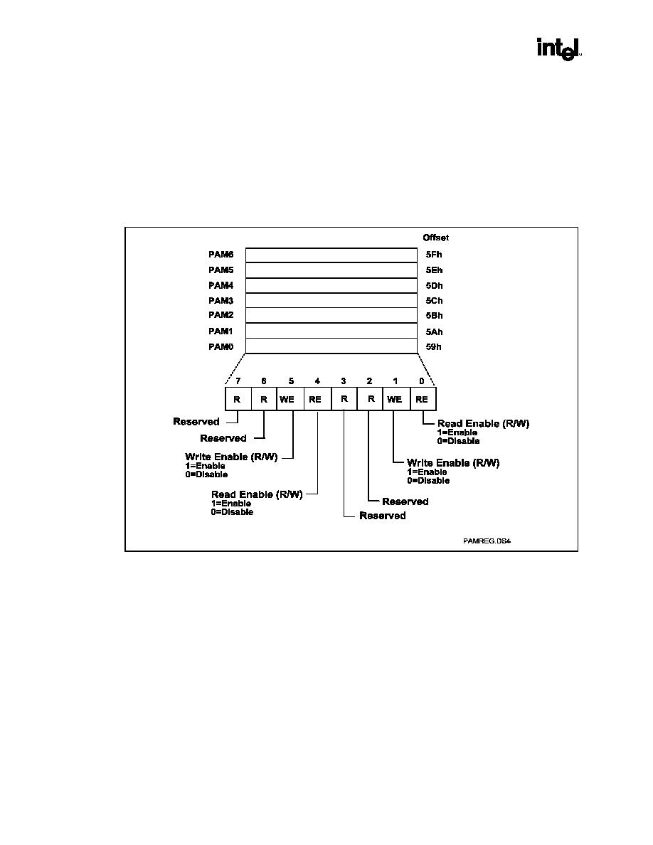
Intel
Æ
830 Chipset Family
86 Datasheet
298338-003
R
As an example, consider a BIOS that is implemented on the expansion bus. During the initialization
process, the BIOS can be shadowed in main memory to increase the system performance. When BIOS is
shadowed in main memory, it should be copied to the same address location. To shadow the BIOS, the
attributes for that address range should be set to write only. The BIOS is shadowed by first doing a read
of that address. This read is forwarded to the expansion bus. The host then does a write of the same
address, which is directed to main memory. After the BIOS is shadowed, the attributes for that memory
area are set to read only so that all writes are forwarded to the expansion bus. Figure 12 and Table 27
show the PAM registers and the associated attribute bits:
Figure 12. PAM Registers

Intel
Æ
830 Chipset Family
298338-003 Datasheet
87
R
Table 27. PAM Registers and Associated Memory Segments
PAM Reg
Attribute Bits
Memory Segment
Comments
Offset
PAM0[3:0]
Reserved
59h
PAM0[7:4]
R R WE RE
0F0000h - 0FFFFFh
BIOS Area
59h
PAM1[3:0]
R R WE RE
0C0000h - 0C3FFFh
ISA Add-on BIOS
5Ah
PAM1[7:4]
R R WE RE
0C4000h - 0C7FFFh
ISA Add-on BIOS
5Ah
PAM2[3:0]
R R WE RE
0C8000h - 0CBFFFh
ISA Add-on BIOS
5Bh
PAM2[7:4]
R R WE RE
0CC000h- 0CFFFFh
ISA Add-on BIOS
5Bh
PAM3[3:0]
R R WE RE
0D0000h- 0D3FFFh
ISA Add-on BIOS
5Ch
PAM3[7:4]
R R WE RE
0D4000h- 0D7FFFh
ISA Add-on BIOS
5Ch
PAM4[3:0]
R R WE RE
0D8000h- 0DBFFFh
ISA Add-on BIOS
5Dh
PAM4[7:4]
R R WE RE
0DC000h- 0DFFFFh
ISA Add-on BIOS
5Dh
PAM5[3:0]
R R WE RE
0E0000h- 0E3FFFh
BIOS Extension
5Eh
PAM5[7:4]
R R WE RE
0E4000h- 0E7FFFh
BIOS Extension
5Eh
PAM6[3:0]
R R WE RE
0E8000h- 0EBFFFh
BIOS Extension
5Fh
PAM6[7:4]
R R WE RE
0EC000h- 0EFFFFh
BIOS Extension
5Fh
For details on overall system address mapping scheme see the Address Decoding Section of this
document.
DOS Application Area (00000h-9FFFh)
The DOS area is 640 KB in size and it is further divided into two parts. The 512-KB area at 0 to 7FFFFh
is always mapped to the main memory controlled by the GMCH-M, while the 128-KB address range
from 080000 to 09FFFFh can be mapped to PCI0 or to main SDRAM. By default, this range is mapped
to main memory and can be declared as a main memory hole (accesses forwarded to PCI0) via GMCH-
M's FDHC configuration register.
Video Buffer Area (A0000h-BFFFFh)
This 128-KB area is not controlled by attribute bits. The host -initiated cycles in this region are always
forwarded to either PCI0 or AGP/PCI1 or PCI2 unless this range is accessed in SMM mode. Routing of
accesses is controlled by the Legacy VGA control mechanism of the "virtual" PCI-PCI bridge device
embedded within the GMCH-M.
This area can be programmed as SMM area via the SMRAM register. When used as an SMM space, this
range cannot be accessed from Hub Interface or AGP.
Expansion Area (C0000h-DFFFFh)
This 128-KB area is divided into eight 16-KB segments that can be assigned with different attributes via
PAM control register as defined by Table 27.
Extended System BIOS Area (E0000h-EFFFFh)
This 64-KB area is divided into four 16-KB segments that can be assigned with different attributes via
PAM control register as defined by the Table 27.

Intel
Æ
830 Chipset Family
88 Datasheet
298338-003
R
System BIOS Area (F0000h-FFFFFh)
This area is a single 64-KB segment that can be assigned with different attributes via PAM control
register as defined by the Table 27.
4.5.1.19
DRB -- DRAM Row Boundary Register - Device #0
Address Offset:
60-67h
Default Value:
00h
Access:
Read/Write (Read_Only if D_LCK = 1)
Size:
8
bits
Row Boundary Register defines the upper boundary address of each SDRAM row in 32-MB granularity.
Each row has its own DRB register. Contents of these 8-bit registers represent the boundary address in
32-MB granularity. For example, a value of 1 indicates 32 MB.
Row0: 60h
Row1: 61h
Row2: 62h
Row3: 63h
Row4: 64h:
Reserved
Row5: 65h:
Reserved
Row6: 66h:
Reserved
Row7: 67h:
Reserved
DRB0 = Total memory in row0 (in 32 Mbytes)
DRB1 = Total memory in row0 + row1 (in 32 Mbytes)
----
DRB4 = Total memory in row0 + row1 + row2 + row3 + (in 32 Mbytes)
Note: The number of DRB registers and number of bits per DRB register are system dependent. For example, a
system that supports 4 rows of SDRAM and a max memory of 1.0 GB needs only 4 DRB registers and 4
bits per DRB.
GMCH-M supports four physical rows of Single data rate SDRAM in 2 SO-DIMMs. The width of a row
is 64 bits. Each SO-DIMM/Row is represented by a byte. Each byte has the following format.
GMCH-M supported maximum memory size: 1.0 GB.
Bit Description
7:0
SDRAM Row Boundary Address: This 8-bit value defines the upper and lower addresses for each SDRAM
row.
Bits 6:0 of this field are compared against the address lines A[31:25] to determine the upper address limit of
a particular row.
Bit 7 must be Zero.
Default Value=0000/0000.

Intel
Æ
830 Chipset Family
298338-003 Datasheet
89
R
4.5.1.20
DRA -- DRAM Row Attribute Register - Device #0
Address Offset:
70-71h
Default Value:
FFh
Access:
Read/Write (Read_Only if D_LCK = 1)
Size:
8
bits
Row0, 1:
70h
Row2, 3:
71h
Row Attribute Register defines the page size of each row.
7 6
4
3
2 0
R
Row attribute for Row1
R
Row Attribute for Row0
7 6
4
3
2 0
R
Row attribute for Row3
R
Row Attribute for Row2
Bit Description
3:0(7:4)
Row Attribute: This 4-bit filed defines the page size of the row. Page Size is dependent on the
technology as shown in the table below.
Bits 3:0 Page Size
"0000" 2 KB
"0001" 4 KB
"0010" 8 KB
"0011" 16 KB.
"1111" Empty Row.
All Other Combinations are Reserved.
Default Value=1111.

Intel
Æ
830 Chipset Family
90 Datasheet
298338-003
R
4.5.1.21
DRT--DRAM Timing Register - Device #0
Address Offset:
78-7Bh
Default Value:
00000010h
Access:
Read/Write
Size:
32
bits
This register controls the timing of the SDRAM Controller.
Bit Description
31:19
Reserved
18:16
DRAM Idle Timer: This field determines the number of clocks the SDRAM controller allows a row in
the idle state (un-accessed) before pre-charging all pages in that row; or powering down that row
based on the settings of bit 28 and bit 14 of DRC.
Bit[18:16] Idle clocks before Action
0 0 0 Infinite (Counter is disabled and no action is taken)
0 0 1
0 (Not Supported on GMCH-M as this setting requires auto precharge)
0 1 0
8
0 1 1
16
1 0 0
64
1 0 1
256
1 1 0
512
1 1 1 1024
DRC 28 DRC 14 Action on Counter Expiration.
(Pwr Dwn Enbl) (Page Cls Enbl)
0
0
None (Counter Disabled)
0
1
Pre-Charge All
1
0
Power Down and Deassert CKE, Pages open.
1
1
Pre-charge All, Power Down and Deassert CKE
Default Value=000.
Recommended settings for DRC 28=1, DRC 14=1 and DRT 18:16 =010.
15:11
Reserved
10
Activate to Precharge delay (tRAS). This bit controls the number of CLKs for tRAS.
0 = tRAS = 7 CLKs
1 = tRAS = 5 CLKs.
Default Value=0.
9:6
Reserved
5:4
CAS# Latency (tCL). This bit controls the number of CLKs between when a read command is
sampled by the SDRAM and when GMCH-M samples read data from the SDRAM.
00 = Reserved
01 = 3
10 = 2
11 = Reserved
Default Value=01.
3
Reserved

Intel
Æ
830 Chipset Family
298338-003 Datasheet
91
R
Bit Description
2
DRAM RAS# to CAS# Delay (tRCD). This bit controls the number of CLKs from a Row Activate
command to a read or write command.
0 = 3 clocks will be inserted between a row activate command and either a read or write command.
1 = 2 clocks will be inserted between a row activate command and either a read or write command.
Default Value=0.
1
Reserved
0
DRAM RAS# Precharge (tRP). This bit controls the number of CLKs for RAS# pre-charge.
0 = 3 clocks of RAS# pre-charge are provided.
1 = 2 clocks of RAS# pre-charge are provided
Default Value=0.

Intel
Æ
830 Chipset Family
92 Datasheet
298338-003
R
4.5.1.22
DRC - DRAM Controller Mode Register - Device #0
Address Offset:
7C-7Fh
Default Value:
00000000h
Access:
Read/Write
Size:
32
bits
Bit Description
31:30
Specification Revision Number. Hardwired to "00" on GMCH-M.
29
Initialization Complete (IC): Setting this bit to a "1" enables SDRAM refreshes. On power up and S3 exit,
the BIOS initializes the SDRAM array and sets this bit to a "1". This bit works in combination with the RMS
bits in controlling refresh state:
IC RMS Refresh State
0 XXX OFF
X 000 OFF
1 001 ON
1 010 ON
1 011 ON
1 111 ON
Default Value=0.
28
DRAM Row Power- Mgmt Enable: When this bit is set to a 1, a SDRAM row is powered down (issued a
power down command and CKE deasserted) after the SDRAM idle timer (as programmed in DRT) expires.
During a refresh, rows in the low power state are powered up and refreshed. Hence, coming out of a refresh
all rows will be powered up.
Default Value=0.
27
Reserved.
26:24
Active Row Count: This field determines the number of rows the SDRAM controller allows in the active state
if SDRAM row power management is enabled (bit 28). All populated rows not in the active state are in power
down. An access to a row in power down will cause that row to exit power down, following that the LRU row
is placed into power down if the number of active rows is greater than that allowed by this register (see BIOS
specification for the latest value. To receive the BIOS specification, contact your Intel Field Representative).
Bit[26:24] Maximum number of Active Rows
0 0 0
All rows allowed to be in active state.
0 0 1
1 Row
0 1 0
2 Rows
0 1 1
3 Rows
1 0 0
4 Rows
1 0 1
Reserved
1 1 0
Reserved
1 1 1
Reserved
Default Value=000.
23:20
Reserved
19:15
Reserved
14
Page Close Enable: When this bit is set to a 1, SDRAM row pages are closed after the SDRAM idle timer
(as programmed in DRT) expires.
Default Value=0.
13:11
Reserved

Intel
Æ
830 Chipset Family
298338-003 Datasheet
93
R
Bit Description
10:8
Refresh Mode Select (RMS): Bits Determine if Refresh is enabled and Refresh Rate.
000: Refresh Disabled.
001: Refresh Enabled. Refresh interval 15.6
µ
s.
010: Refresh Enabled. Refresh interval 7.8
µ
s.
011: Reserved
111: Refresh Enabled. Refresh interval 128 Clocks. (Fast Refresh Mode)
All Other Combinations are reserved.
Default Value=000.
7
Reserved
6:4
Mode Select (SMS). These bits select the special operational mode of the GMCH-M SDRAM interface. The
special modes are intended for initialization at power up.
000 = Self refresh (Default):
In this mode, CKEs are deasserted. All other values cause CKE assertion. The exception is in
C3/S1/S3 this register is programmed to "normal operation", the DRAMs are in self-refresh, and CKEs
are deasserted.
001 = NOP Command Enable:
In this mode all CPU cycles to SDRAM result in a NOP Command on the SDRAM interface.
010 = All Banks Pre-charge Enable:
In this mode all CPU cycles to SDRAM result in an All Banks Pre-charge Command on the SDRAM
interface.
011 = Mode Register Set Enable:
In this mode all CPU cycles to SDRAM result in a mode register set command on the SDRAM
interface. The Command is driven on the MA[12:0] lines. MA[2:0] must always be driven to 010 for
burst of 4 mode. MA3 must be driven to 1 for interleave wrap type.
MA[6:4] needs to be driven based on the value programmed in the CAS# Latency field.
CAS
Latency
MA[6:4]
2 Clocks
010
3 Clocks
011
MA[12:7] must be driven to 00000.
BIOS must calculate and drive the correct host address for each row of memory such that the correct
command is driven on the MA[12:0] lines.
100 = Reserved.
101 = Reserved.
110 = CBR Refresh Enable. In this mode all CPU cycles to SDRAM result in a CBR cycle on the SDRAM
interface.
111 = Normal Operation.
Default Value=000.
3:2
Reserved
1:0
Reserved

Intel
Æ
830 Chipset Family
94 Datasheet
298338-003
R
4.5.1.23
DTC - DRAM Throttling Control Register - Device #0.
Offset Address:
8C-8Fh
Default Value:
0000_0000h
Access:
Read/Write/Lock
Size:
32
bits
Throttling is independent for Reads and Writes. If the number of Oct-Words (16 bytes) read/written
during this window exceeds the DRAM Bandwidth Threshold defined below, then the DRAM throttling
mechanism will be invoked to limit DRAM reads/writes to a lower bandwidth checked over smaller time
windows. The throttling will be active for the remainder of the current GDWS and for the next GDSW
after which it will return to non-throttling mode. The throttling mechanism accounts for the actual
bandwidth consumed during the sampling window, by reducing the allowed bandwidth within the
smaller throttling window based on the bandwidth consumed during the sampling period.
Bits Description
31
Throttle Lock (TLOCK): This bit secures the SDRAM throttling control register. Once a `1' is written to
this bit, all of the configuration register bits in DTC (including TLOCK) documented below become read-
only.
Default Value=0.
30
Intel Reserved
29:28
DRAM Throttle Mode (TMODE):
Bits Mode
0 0
Throttling turned off.
0 1 Bandwidth Counter mechanism is enabled. When bandwidth exceeds threshold set in the r/w PTC
field, DRAM read/write throttling begins.
1 0 Thermal Sensor based throttling enabled. When the device's thermal sensor is tripped DRAM
Write throttling begins based on settings programmed in WPTC. Read throttling is disabled.
1 1 With this setting Thermal Sensor and DRAM Counter mechanisms are both enabled. However,
read throttling is bandwidth counter triggered only while write throttling is thermal sensor or counter
triggered. Both read and write throttling mechanisms use programmed values in the throttle control
registers.
Default Value=00
27:26
Reserved
25:24
Read Power Throttle Control. These bits select the Power Throttle Bandwidth Limits for Read operations
to System Memory.
R/W, RO if Throttle Lock.
Bits Power Throttle Bandwidth Limit
00 No Limit (Default)
01 Limit at 65%
10 Limit at 55%
11 Limit at 45%
Default Value=00
23:22
Reserved
21:20
Write Power Throttle Control. These bits select the Power Throttle Bandwidth Limits for Write operations
to System Memory.

Intel
Æ
830 Chipset Family
298338-003 Datasheet
95
R
Bits Description
R/W, RO if Throttle Lock.
Bits Power Throttle Bandwidth Limit
00 No Limit (Default)
01 Limit at 65%
10 Limit at 55%
11 Limit at 45%
Default Value=00
19:16
Reserved
15:8
Global DRAM Sampling Window (GDSW): This eight bit value is multiplied by 4 to define the length of
time in milliseconds (0-1020) over which the number of OctWords (16 bytes) read/written is counted and
Throttling is imposed.
Default Value=00000000.
7:0
Reserved

Intel
Æ
830 Chipset Family
96 Datasheet
298338-003
R
4.5.1.24
SMRAM - System Management RAM Control Register - Device #0
Address Offset:
90h
Default Value:
02h
Access:
Read/Write/Lock, Read Only
Size:
8
bits
The SMRAM register controls how accesses to Compatible and Extended SMRAM spaces are treated.
The Open, Close, and Lock bits function only when G_SMRAME bit is set to a 1. Also, the OPEN bit
must be reset before the LOCK bit is set.
Bit Description
7
Reserved
6
SMM Space Open (D_OPEN): When D_OPEN=1 and D_LCK=0, the SMM space SDRAM is made
visible even when SMM decode is not active. This is intended to help BIOS initialize SMM space.
Software should ensure that D_OPEN=1 and D_CLS=1 are not set at the same time.
When D_LCK is set to a 1, D_OPEN is reset to 0 and becomes read only.
Default Value=0.
5
SMM Space Closed (D_CLS): When D_CLS = 1 SMM space DRAM is not accessible to data
references, even if SMM decode is active. Code references may still access SMM space SDRAM. This
will allow SMM software to reference "through" SMM space to update the display even when SMM is
mapped over the VGA range.
Software should ensure that D_OPEN=1 and D_CLS=1 are not set at the same time.
Default Value=0.
4
SMM Space Locked (D_LCK): When D_LCK is set to 1 then D_OPEN is reset to 0 and D_LCK,
D_OPEN, G_SMRAME, C_BASE_SEG, GMS, DRB, DRA, H_SMRAM_EN, TSEG_SZ and TSEG_EN
become read only.
GBA[15:0] and GAR[15:0] associated with the SDRAM controller also become read only after D_LCK is
set. D_LCK can be set to 1 via a normal configuration space write but can only be cleared by a Full
Reset. The combination of D_LCK and D_OPEN provide convenience with security. The BIOS can use
the D_OPEN function to initialize SMM space and then use D_LCK to "lock down" SMM space in the
future so that no application software (or BIOS itself) can violate the integrity of SMM space, even if the
program has knowledge of the D_OPEN function.
Default Value=0.
3
Global SMRAM Enable (G_SMRAME). If set to a 1, then Compatible SMRAM functions is enabled,
providing 128 KB of SDRAM accessible at the A0000h address while in SMM (ADS# with SMM
decode).
To enable Extended SMRAM function this bit has be set to 1.
Refer to the section on SMM for more details. Once D_LCK is set, this bit becomes read only.
Default Value=0.
2:0
Compatible SMM Space Base Segment (C_BASE_SEG) (RO). This field indicates the location of
SMM space. "SMM DRAM" is not remapped. It is simply "made visible" if the conditions are right to
access SMM space, otherwise the access is forwarded to Hub Interface.
C_BASE_SEG is hardwired to 010 to indicate that the GMCH-M supports the SMM space at A0000h-
BFFFFh.
Default Value=010.
Intel
Æ
830 Chipset Family
298338-003 Datasheet
97
R
4.5.1.25
ESMRAMC - Extended System Management RAM Control Register -
Device #0
Address Offset:
91h
Default Value:
38h
Access:
Read/Write
Size:
8
bits
The Extended SMRAM register controls the configuration of Extended SMRAM space. The Extended
SMRAM (E_SMRAM) memory provides a write-back cacheable SMRAM memory space that is above
1 MB.
Bit Description
7
H_SMRAM_EN (H_SMRAME): Controls the SMM memory space location (i.e. above 1 MB or below 1
MB). When G_SMRAME is 1 and H_SMRAME this bit is set to 1, the high SMRAM memory space is
enabled. SMRAM accesses from 0FEDA0000h to 0FEDBFFFFh are remapped to SDRAM address
000A0000h to 000BFFFFh.
Once D_LCK is set, this bit becomes read only.
Default Value=0.
6
E_SMRAM_ERR (E_SMERR): This bit is set when CPU accesses the defined memory ranges in
Extended SMRAM (High Memory and T-segment) while not in SMM space and with the D-OPEN bit = 0.
It is software's responsibility to clear this bit. The software must write a 1 to this bit to clear it
Default Value=0.
5
SMRAM_Cache (SM_CACHE): This bit is forced to `1' by the GMCH-M .
Default Value=1.
4
SMRAM_L1_EN (SM_L1): This bit is forced to `1' by the GMCH-M.
Default Value=1.
3
SMRAM_L2_EN (SM_L2): This bit is forced to `1' by the GMCH-M.
Default Value=1.
2
Reserved
1
TSEG_SZ(T_SZ): Selects the size of the TSEG memory block if enabled. This memory is taken from
the top of SDRAM space (i.e. TOM - TSEG_SZ), which is no longer claimed by the memory controller.
This field decodes as follows:
TSEG_SZ Description
0 (TOM-512K) to TOM
1 (TOM-1M) to TOM
Once D_LCK is set, this bit becomes read only.
Default Value=0.
0
TSEG_EN (T_EN): Enabling of SMRAM memory (TSEG, 512 Kbytes or 1 Mbytes of additional SMRAM
memory) for Extended SMRAM space only. When G_SMRAME =1 and TSEG_EN = 1, the TSEG is
enabled to appear in the appropriate physical address space.
Once D_LCK is set, this bit becomes read only.
Default Value=0.

Intel
Æ
830 Chipset Family
98 Datasheet
298338-003
R
4.5.1.26
ERRSTS ≠ Error Status Register ≠ Device #0
Address Offset:
92-93h
Default Value:
0000h
Access: Read/Write
Clear
Size: 16
bits
This register is used to report various error conditions via Hub interface special cycles. An SERR, SMI,
or SCI Error Hub interface special cycle may be generated on a zero to one transition of any of these
flags when enabled in the PCICMD/ERRCMD, SMICMD, or SCICMD registers respectively.
Bit Description
15:13
Reserved
12
GMCH Software Generated Event for SMI. This indicates the source of the SMI was a Device#2
Software Event for the Local Memory Interface. Software must write a "1" to clear this bit. (Local memory
no longer supported.)
11
Reserved
10
Reserved
9
LOCK to non-DRAM Memory Flag (LCKF). (R/WC) When this bit is set it indicates that a CPU initiated
LOCK cycle targeting non-DRAM memory space occurred. Software must write a "1" to clear this status
bit.
8
Received Refresh Timeout.
This Bit is set when 1024 memory core refresh are Queued up.
Software must write a "1" to clear this status bit.
7
DRAM Throttle Flag (DTF) (R/WC). When this bit is set it indicates that the DRAM Throttling condition
occurred. Software must write a "1" to clear this status bit.
6
Reserved
5
Received Unimplemented Special Cycle Hub interface Completion Packet FLAG (UNSC) (R/WC).
When this bit is set, it indicates that the GMCH initiated a Hub interface request that was terminated with
an Unimplemented Special Cycle completion packet. Software must write a "1" to clear this status bit.
4
AGP Access Outside of Graphics Aperture Flag (OOGF). (R/WC) When this bit is set it indicates that
an AGP access occurred to an address that is outside of the graphics aperture range. Software must
write a "1" to clear this status bit.
Note: AGP is available only with the Intel 830M and 830MP Chipset.
3
Invalid AGP Access Flag (IAAF). (R/WC) When this bit is set to "1" it indicates that an AGP access
was attempted outside of the graphics aperture and either to the 640k - 1M range or above the top of
memory. Software must write a "1" to clear this status bit.
NOTE: AGP is available only with the Intel 830M and 830MP Chipset.
2
Invalid Graphics Aperture Translation Table Entry Flag (ITTEF). (R/WC) When this bit is set to "1", it
indicates that an invalid translation table entry was returned in response to an AGP access to the
graphics aperture.
Software must write a "1" to clear this status bit.
Invalid translation table entries include the following:
Invalid bit set in table entry.
Translated address hits PAM region.
Translated address hits enabled physical SMM space.
NOTE: AGP is available only with the Intel 830M and 830MP Chipset.
1-0
Reserved

Intel
Æ
830 Chipset Family
298338-003 Datasheet
99
R
4.5.1.27
ERRCMD - Error Command Register - Device #0
Address Offset:
94-95h
Default Value:
0000h
Access:
Read/Write
Size:
16
bits
This register enables various errors to generate an SERR Hub Interface special cycle. Since the GMCH-
M does not have an SERR# signal, SERR messages are passed from the GMCH-M to the ICH3-M over
the Hub Interface. The actual generation of the SERR message is globally enabled for Device #0 via the
PCI Command register.
Note: An error can generate one and only one Hub Interface error special cycle. The software is responsible to
ensure that when an SERR error message is enabled for an error condition, SMI and SCI error messages
are disabled for that same error condition.
Bit Description
15:10
Reserved
9
SERR on LOCK to non-SDRAM Memory. When this bit is set to "1", the GMCH-M generates an SERR
Hub Interface special cycle when a CPU initiated LOCK transaction targeting non-SDRAM memory space
occurs.
If this bit is "0" then reporting of this condition is disabled.
Default Value=0.
8
SERR on SDRAM Refresh timeout. When this bit is set to "1", the GMCH-M generates an SERR Hub
Interface special cycle when a SDRAM Refresh timeout occurs.
If this bit is "0" then reporting of this condition is disabled.
Default Value=0.
7
SERR on SDRAM Throttle Condition. When this bit is set to "1", the GMCH-M generates an SERR Hub
Interface special cycle when a SDRAM Read or Write Throttle condition occurs.
If this bit is "0" then reporting of this condition is disabled.
Default Value=0.
6
SERR on Receiving Target Abort on Hub Interface. When this bit is set to "1", the GMCH-M generates
an SERR Hub Interface special cycle when a GMCH-M originated Hub Interface cycle is terminated with a
Target Abort.
If this bit is "0" then reporting of this condition is disabled.
Default Value=0.
5
SERR on Receiving Unimplemented Special Cycle Hub Interface Completion Packet. When this bit is
set to "1", the GMCH-M generates an SERR Hub Interface special cycle when a GMCH-M initiated Hub
Interface request is terminated with a Unimplemented Special Cycle completion packet.
If this bit is "0" then reporting of this condition is disabled.
Default Value=0.
4
SERR on AGP Access Outside of Graphics Aperture. When this bit is set to "1", the GMCH-M
generates an SERR Hub Interface special cycle when an AGP access occurs to an address outside of the
graphics aperture.
If this bit is "0" then reporting of this condition is disabled.
Default Value=0.
NOTE: AGP is available only with the Intel 830M and 830MP Chipset.
3
SERR on Invalid AGP Access. When this bit is set to "1", the GMCH-M generates an SERR Hub
Interface special cycle when an AGP access occurs to an address outside of the graphics aperture and
either to the 640K - 1M range or above the top of memory.

Intel
Æ
830 Chipset Family
100 Datasheet
298338-003
R
Default Value=0.
NOTE: AGP is available only with the Intel 830M and 830MP Chipset.
2
SERR on Access to Invalid Graphics Aperture Translation Table Entry. When this bit is set to "1", the
GMCH-M generates an SERR Hub Interface special cycle when an invalid translation table entry was
returned in response to a AGP access to the graphics aperture.
If this bit is "0" then reporting of this condition via SERR messaging is disabled.
Default Value=0.
NOTE: AGP is available only with the Intel 830M and 830MP Chipset.
1-0
Reserved
Table 28. Summary of GMCH-M Error Sources, Enables and Status Flags
Error Event
Hub I/F
Message
Enable Bits Required
to be Set
Status Flags Set
SDRAM Refresh Timeout
SERR
PCICMD bit 8
ERRCMD bit 8
PCISTS bit 14
ERRSTS bit 8
CPU LOCK to non-SDRAM memory
SERR
PCICMD bit 8
ERRCMD bit 9
PCISTS bit 14
ERRSTS bit 9
SDRAM Throttle
SERR
PCICMD bit 8
ERRCMD bit 7
PCISTS bit 14
ERRSTS bit 7
Received Hub Interface Target Abort
SERR
PCICMD bit 8
ERRCMD bit 6
PCISTS bit 14
PCISTS bit 12
Unimplemented Special Cycle
SERR
PCICMD bit 8
ERRCMD bit 5
PCISTS bit 14
ERRSTS bit 5
AGP Access Outside of Graphics Aperture
SERR
PCICMD bit 8
ERRCMD bit 4
PCISTS bit 14
ERRSTS bit 4
Invalid AGP Access
SERR
PCICMD bit 8
ERRCMD bit 3
PCISTS bit 14
ERRSTS bit 3
Access to Invalid GTLB Entry
SERR
PCICMD bit 8
ERRCMD bit 2
PCISTS bit 14
ERRSTS bit 2
AGP PCI Parity Error Detected
SERR
PCICMD1 bit 8
BCTRL bit 0
PCISTS1 bit 14
SSTS bit 15
AGP PCI Received Target Abort
SERR
PCICMD1 bit 8
ERRCMD1 bit 0
PCISTS1 bit 14
SSTS bit 12
Intel
Æ
830 Chipset Family
298338-003 Datasheet
101
R
4.5.1.28
ACAPID - AGP Capability Identifier Register - Device #0
Address Offset:
A0-A3h
Default Value:
00200002h
Access:
Read
Only
Size:
32
bits
This register provides standard identifier for AGP capability. This register is Read Only when either the
Intel 830M or Intel 830MG internal graphics device is used.
Bit Description
31:24
Reserved
23:20
Major AGP Revision Number: These bits provide a major revision number of AGP specification to
which this version of GMCH-M conforms. These bits are set to the value 0010 to indicate AGP Rev. 2.x.
Default Value=0010.
19:16
Minor AGP Revision Number: These bits provide a minor revision number of AGP specification to
which this version of GMCH-M conforms. This number is hardwired to value of 0000 (i.e. implying Rev
x.0). Together with major revision number, this field identifies GMCH-M as an AGP REV 2.0 compliant
device.
Default Value=0000.
15:8
Next Capability Pointer: AGP capability is the last capability described via the capability pointer
mechanism and therefore these bits are hardwired to 00h to indicate the end of the capability linked list.
Default Value=0000/0000.
7:0
AGP Capability ID: This field identifies the linked list item as containing AGP registers. This field has the
value 02h as assigned by the PCI SIG.
Default Value=0000/0010.

Intel
Æ
830 Chipset Family
102 Datasheet
298338-003
R
4.5.1.29
AGPSTAT - AGP Status Register - Device #0
Address Offset:
A4-A7h
Default Value:
1F000217h
Access:
Read
Only
Size:
32
bits
This register reports AGP device capability/status. This register is Read Only when either the Intel 830M
or Intel 830MG internal graphics device is used.
Bit Description
31:24
Request Queue. This field is hardwired to 1Fh to indicate a maximum of 32 outstanding AGP
command requests can be handled by the GMCH-M. Default =1Fh to allow a maximum of 32
outstanding AGP command requests.
Default Value=00011111.
23:10
Reserved
9
SBA. This bit indicates that the GMCH-M supports side band addressing.
It is hardwired to 1.
8:6
Reserved
5
4G. This bit indicates that the GMCH-M does not support addresses greater than 4 GB.
It is hardwired to 0.
4
Fast Writes
The GMCH-M supports Fast Writes from the CPU to the AGP master.
Fast Writes are disabled.
Default Value=1.
3
Reserved
2:0
RATE. After reset the GMCH-M reports its data transfer rate capability.
Bit 0 identifies if AGP device supports 1x data transfer mode
Bit 1 identifies if AGP device supports 2x data transfer mode
Bit 2 identifies if AGP device supports 4x data transfer mode.
1x, 2x, and 4x data transfer modes are supported by the GMCH-M.
NOTE: The selected data transfer mode applies to both AD bus and SBA bus.
Default Value=111.

Intel
Æ
830 Chipset Family
298338-003 Datasheet
103
R
4.5.1.30
AGPCMD - AGP Command Register - Device #0
Address Offset:
A8-ABh
Default Value:
00000000h
Access:
Read/Write
Size:
32
bits
This register provides control of the AGP operational parameters. This register is Read Only when
either the Intel 830M or Intel 830MG internal graphics device is used.
Bit Description
31:10
Reserved
9
SBA Enable. When this bit is set to 1, the side band addressing mechanism is enabled.
Default Value=0.
8
AGP Enable. When this bit is reset to 0, the GMCH-M will ignore all AGP operations, including the sync
cycle.
Any AGP operations received while this bit is set to 1 will be serviced even if this bit is reset to 0.
If this bit transitions from a 1 to a 0 on a clock edge in the middle of an SBA command being delivered in
1X mode the command will be issued.
When this bit is set to 1 the GMCH-M will respond to AGP operations delivered via PIPE#, or to operations
delivered via SBA if the AGP Side Band Enable bit is also set to 1.
Default Value=0.
7:6
Reserved
5
4G. The GMCH-M as an AGP target does not support addressing greater than 4 GB. This bit is hardwired
to 0.
4
Fast Write Enable
When set to "1" GMCH-M AGP master supports Fast Writes.
When set to "0" Fast Writes are disabled.
Default Value=0.
3
Reserved
2:0
Data Rate: The settings of these bits determine the AGP data transfer rate. One (and only one) bit in this
field must be set to indicate the desired data transfer rate.
001 = 1X (Bit 0)
010 = 2X (Bit 1)
100 = 4x (Bit 2)
The same bit must be set on both master and target. Configuration software will update this field by setting
only one bit that corresponds to the capability of AGP master (after that capability has been verified by
accessing the same functional register within the AGP masters configuration space.)
Note that the selected data transfer mode applies to both AD bus and SBA bus.
Default Value=000

Intel
Æ
830 Chipset Family
104 Datasheet
298338-003
R
4.5.1.31
AGPCTRL - AGP Control Register - Device #0
Address Offset:
B0-B1h
Default Value:
00000000h
Access:
Read/Write
Size:
32
bits
This register provides for additional control of the AGP interface. This register is Read Only when either
the Intel 830M or Intel 830MG internal graphics device is used.
Bit Description
31:8
Reserved
7
GTLB Enable (and GTLB Flush Control) (R/W):
NOTE: This bit can be changed dynamically (i.e. while an access to GTLB occurs).
Default Value=0.
6:0
Reserved
4.5.1.32
AFT ≠ AGP Functional Test Register ≠ Device #0
Address Offset:
B2-B3h
Default Value:
0000h
Access: Read/Write
Size: 16
bits
This register provides for additional control of the AGP interface. This register is Read Only when
either the Intel 830M or Intel 830MG internal graphics device is used.
Bit Description
15:10
Reserved
9
PCI Read Buffer Disable. (RW) When set to "1" is disabled. In this mode all data pre-fetched and
buffered for a PCI-to-DRAM read will be discarded when that read transaction terminates.
This bit defaults to "0".
8:4
AGP PCI1 Discard Timer Time-out Count. (RW) These bits control the length of AGP/PCI1
Delayed Transaction discard time-out for the purpose of enhancing the system testability.
Default value is 11111b (31d) for a discard count of 1024d ((value+1)*32).
3:0
Reserved

Intel
Æ
830 Chipset Family
298338-003 Datasheet
105
R
4.5.1.33 APSIZE
Aperture Size - Device #0
Address Offset:
B4h
Default Value:
00h
Access:
Read/Write
Size:
8
bits
This register determines the effective size of the Graphics Aperture. This register can be updated by the
GMCH-M-specific BIOS configuration sequence before the PCI standard bus enumeration sequence. If
the register is not updated then a default value will select an aperture of maximum size (i.e. 256 MB).
The size of the table that will correspond to a 256 MB aperture is not practical for most applications and
therefore these bits must be programmed to a smaller practical value that will force adequate address
range to be requested via APBASE register from the PCI configuration software. This register is Read
Only when either the Intel 830M or Intel 830MG internal graphics device is used.
Bit Description
7:6
Reserved
5:3
Graphics Aperture Size (APSIZE) (R/W): Each bit in APSIZE[5:3] operates on similarly ordered bits in
APBASE[27:25] of the Aperture Base configuration register.
When a particular bit of this field is "0", it forces the similarly ordered bit in APBASE[27:25] to behave as
"hardwired" to 0.
When a particular bit of this field is set to "1", it allows the corresponding bit of the APBASE[27:25] to be
read/write accessible. Only the following combinations are allowed when the Aperture is enabled:
Bits[5:3] Aperture Size
1 1 1
32 MB
1 1 0
64 MB
1 0 0
128 MB
0 0 0
256 MB
Default for APSIZE[5:3]=000b forces default APBASE[27:25] =000b (i.e. all bits respond as "hardwired" to 0).
This provides maximum aperture size of 256 MB. As another example, programming APSIZE[5:3]=111b
enables APBASE[27:25] as read/write programmable.
2:0
Reserved

Intel
Æ
830 Chipset Family
106 Datasheet
298338-003
R
4.5.1.34 ATTBASE
Aperture Translation Table Base Register - Device #0
Address Offset:
B8-BBh
Default Value:
00000000h
Access:
Read/Write
Size:
32
bits
This register provides the starting address of the Graphics Aperture Translation Table Base located in the
main DRAM. This value is used by the GMCH-M's Graphics Aperture address translation logic
(including the GTLB logic) to obtain the appropriate address translation entry required during the
translation of the aperture address into a corresponding physical DRAM address. The ATTBASE
register may be dynamically changed. This register is Read Only when either the Intel 830M or Intel
830MG internal graphics device is used.
Note: The address provided via ATTBASE is 4-KB aligned.
Bit Description
31: 12
This field contains a pointer to the base of the translation table used to map memory space addresses in
the aperture range to addresses in main memory.
11:0
Reserved
4.5.1.35 AMTT
AGP Interface Multi-Transaction Timer Register - Device #0
Address Offset:
BCh
Default Value:
00h
Access:
Read/Write
Size:
8
bits
AMTT is an 8-bit register that controls the amount of time that the GMCH-M's arbiter allows the
AGP/PCI master to perform multiple back-to-back transactions. The GMCH-M's AMTT mechanism is
used to optimize the performance of the AGP master (using PCI semantics) that performs multiple back-
to-back transactions to fragmented memory ranges (and as a consequence cannot use long burst
transfers). The AMTT mechanism applies to the CPU-AGP/PCI transactions as well and it guarantees to
the CPU a fair share of the AGP/PCI interface bandwidth.
The number of clocks programmed in the AMTT represents the guaranteed time slice (measured in 66-
MHz clocks) allotted to the current agent (either AGP PCI master or Host bridge) after which the AGP
arbiter may grant the bus to another agent. The default value of AMTT is 00h and disables this function.
The AMTT value can be programmed with 8-clock granularity. For example, if the AMTT is
programmed to 18h, then the selected value corresponds to the time period of 24 AGP (66-MHz) clocks.
This register is Read Only when either the Intel 830M or Intel 830MG internal graphics device is used.
Bit Description
7:3
Multi-Transaction Timer Count Value. The number programmed in these bits represents the guaranteed
time slice (measured in eight 66-MHz clock granularity) allotted to the current agent (either AGP PCI master
or Host bridge) after which the AGP arbiter may grant the bus to another agent.
2:0
Reserved

Intel
Æ
830 Chipset Family
298338-003 Datasheet
107
R
4.5.1.36 LPTT
Low Priority Transaction Timer Register - Device #0
Address Offset:
BDh
Default Value:
00h
Access:
Read/Write
Size:
8
bits
LPTT is an 8-bit register similar in a function to AMTT. This register is used to control the minimum
tenure on the AGP for low priority data transaction (both reads and writes) issued using PIPE# or
Sideband mechanisms.
The number of clocks programmed in the LPTT represents the guaranteed time slice (measured in 66-
MHz clocks) allotted to the current low priority AGP transaction data transfer state. This does not
necessarily apply to a single transaction but it can span over multiple low-priority transactions of the
same type. After this time expires the AGP arbiter may grant the bus to another agent if there is a
pending request. The LPTT does not apply in the case of high-priority request where ownership is
transferred directly to the high-priority requesting queue.
The default value of LPTT is 00h and disables this function. The LPTT value can be programmed with
8-clock granularity. For example, if the LPTT is programmed to 10h, then the selected value corresponds
to the time period of 16 AGP (66-MHz) clocks. This register is Read Only when either the Intel 830M or
Intel 830MG internal graphics device is used.
Bit Description
7:3
Low Priority Transaction Timer Count Value. The number of clocks programmed in these bits
represents the guaranteed time slice (measured in eight 66-MHz clock granularity) allotted to the
current low priority AGP transaction data transfer state.
2:0
Reserved

Intel
Æ
830 Chipset Family
108 Datasheet
298338-003
R
4.5.1.37
BUFF_SC ≠ System Memory Buffer Strength Control Register - Device #0
Address Offset:
EC-EFh
Default Value:
00000000h
Access:
Read/Write
Size
32
bits
4.5.1.37.1
SDR Drive Strength Register Description
The System Memory Buffer Strength Control Register programs drive strengths and slew rate and for
each buffer category based on loading detected by SPD. CS#, CKE, and CLK buffers have independent
control for each SO-DIMM and are programmed to the same strength for front and back side of each
SO-DIMM. If the BIOS detects different loading on the backside of the SO-DIMM (i.e. 96 MB), it
should ignore the devices on the backside of the SO-DIMM.
Bit Descriptions
31
Reserved
30
CLK[3:2] Slew Rate. This field sets the slew rate of the CLK[3:2] pins.
0 = Normal slew rate.
1 = Fast slew rate for reduced Tco.
Default Value=0.
29
CLK[1:0] Slew Rate. This field sets the slew rate of the CLK[1:0] pins.
0 = Normal slew rate.
1 = Fast slew rate for reduced Tco.
Default Value=0.
28
Reserved
27
CS[3:2]#, CKE[3:2] Slew Rate. This field sets the slew rate of the CS[3:2]#, CKE[3:2] pins.
0 = Normal slew rate.
1 = Fast slew rate for reduced Tco.
Default Value=0.
26
CS[1:0]#, CKE[1:0] Slew Rate. This field sets the slew rate of the CS[1:0]#, CKE[1:0] pins.
0 = Normal slew rate.
1 = Fast slew rate for reduced Tco.
Default Value=0.
25
DQ[63:0], DQM[7:0] Slew Rate. This field sets the slew rate of the DQ[63:0], DQM[7:0] pins.
0 = Normal slew rate.
1 = Fast slew rate for reduced Tco.
Default Value=0.
24
MA[12:0], BA[1:0], RAS#, CAS#, WE# Slew Rate. This field sets the slew rate of the MA[12:0],
BA[1:0], RAS#, CAS#, WE# pins.
0 = Normal slew rate.
1 = Fast slew rate for reduced Tco.
Default Value=0.
23:21
Reserved
20:18
CLK[3:2] Buffer Strength. This field sets the buffer strength of the CLK[3:2] pins.

Intel
Æ
830 Chipset Family
298338-003 Datasheet
109
R
000 = 0.75X
001 = 1X
010 = 1.25X
011 = 1.5X
100 = 2X
101 = 2.5X
110 = 3X
111 = 4X
Default Value=000.
17:15
CLK[1:0] Buffer Strength. This field sets the buffer strength of the CLK[1:0] pins.
000 = 0.75X
001 = 1X
010 = 1.25X
011 = 1.5X
100 = 2X
101 = 2.5X
110 = 3X
111 = 4X
Default Value=000.
14:12
RESERVED
11:9
CS[3:2]#, CKE[3:2] Buffer Strength. This field sets the buffer strength of the CS[3:2]#, CKE[3:2]
pins.
000 = 0.75X
001 = 1X
010 = 1.25X
011 = 1.5X
100 = 2X
101 = 2.5X
110 = 3X
111 = invalid
Default Value=000.
8:6
CS[1:0]#, CKE[1:0] Buffer Strength. This field sets the buffer strength of the CS[1:0]#, CKE[1:0]
pins.
000 = 0.75X
001 = 1X
010 = 1.25X
011 = 1.5X
100 = 2X
101 = 2.5X
110 = 3X
111 = invalid
Default Value=000.
5:3
DQ[63:0], DQM[7:0] Buffer Strength. This field sets the buffer strength of the DQ[63:0], DQM[7:0]
pins.
000 = 0.75X
001 = 1X
010 = 1.25X

Intel
Æ
830 Chipset Family
110 Datasheet
298338-003
R
011 = 1.5X
100 = 2X
101 = 2.5X
110 = 3X
111 = invalid
Default Value=000.
2:0
MA[12:0], BA[1:0], RAS#, CAS#, WE# Buffer Strength. This field sets the buffer strength of the
MA[12:0], BA[1:0], RAS#, CAS#, WE# pins.
000 = 0.75X
001 = 1X
010 = 1.25X
011 = 1.5X
100 = 2X
101 = 2.5X
110 = 3X
111 = invalid
Default Value=000.
Intel
Æ
830 Chipset Family
298338-003 Datasheet
111
R
4.5.2
830M and 830MP Chipset HOST-AGP Bridge Registers - Device
#1
Table 29 summarizes the GMCH-M configuration space for device #1. Device 1 applies to both the
Intel 830MP and 830M Chipset.
Table 29. Host-AGP Bridge Configuration Space (Device #1)
Address Offset
Register Symbol
Register Name
Default Value
Access
00-01h VID1
Vendor
Identification
8086h RO
02-03h DID1
Device
Identification
3576h RO
04-05h
PCICMD1
PCI Command Register
0000h
RO, R/W
06-07h
PCISTS1
PCI Status Register
0020h
RO, R/WC
08 RID1 Revision
Identification
00h
RO
09 -
Intel
Reserved
- -
0Ah SUBC1
Sub-Class
Code
04h
RO
0Bh+
BCC1
Base Class Code
06h
RO
0Ch -
Intel
Reserved - -
0Dh MLT1 Master
Latency
Timer
00h
R/W
0Eh HDR1 Header
Type 01h
RO
0F-17h -
Intel
Reserved
-
-
18h PBUSN
Primary
Bus
Number
00h
RO
19h
SBUSN
Secondary Bus Number
00h
R/W
1Ah
SUBUSN
Subordinate Bus Number
00h
R/W
1Bh
SMLT
Secondary Bus Master
Latency Timer
00h R/W
1Ch
IOBASE
I/O Base Address Register
F0h
R/W
1Dh IOLIMIT
I/O
Limit
Address
Register
00h
R/W
1E-1Fh
SSTS
Secondary Status Register
02A0h
RO, R/WC
20-21h MBASE Memory
Base
Address
Register
FFF0h R/W
22-23h MLIMIT Memory
Limit
Address
Register
0000h R/W
24-25h
PMBASE
Prefetchable Memory Base
Address Reg.
FFF0h R/W
26-27h
PMLIMIT
Prefetchable Memory Limit
Address Reg.
0000h R/W
28-3Dh -
Intel
Reserved
-
-
3Eh
BCTRL
Bridge Control Register
00h
R/W
3Fh -
Intel
Reserved - -
40h ERRCMD1
Error
Command
00h
R/W
41-FFh -
Intel
Reserved
-
-

Intel
Æ
830 Chipset Family
112 Datasheet
298338-003
R
4.5.2.1
VID1 - Vendor Identification Register - Device #1
Address Offset:
00 - 01h
Default Value:
8086h
Attribute:
Read Only
Size:
16
bits
The VID Register contains the vendor identification number. This 16-bit register combined with the
Device Identification Register uniquely identifies any PCI device. Writes to this register have no effect.
Bit Description
15:0
Vendor Identification Number. This is a 16-bit value assigned to Intel. Intel VID = 8086h.
Default Value=1000/0000/1000/0110.
4.5.2.2
DID1 - Device Identification Register - Device #1
Address Offset:
02 - 03h
Default Value:
3576h
Attribute:
Read Only
Size:
16
bits
This 16-bit register combined with the Vendor Identification register uniquely identifies any PCI device.
Writes to this register have no effect.
Bit Description
15:0
Device Identification Number. This is a 16-bit value assigned to the GMCH-M device #1.GMCH-M device
#1 DID =3576h.
Default Value=0011/0101/0111/0110.

Intel
Æ
830 Chipset Family
298338-003 Datasheet
113
R
4.5.2.3
PCICMD1 - PCI-PCI Command Register - Device #1
Address Offset:
04-05h
Default Value:
0000h
Access:
Read/Write, Read Only
Size
16
bits
Bit Descriptions
15:10
Reserved
9
Fast Back-to-Back: Not Applicable-hardwired to 0.
Default Value=0.
8
SERR Message Enable (SERRE1). This bit is a global enable bit for Device #1 SERR messaging. The
GMCH-M does not have an SERR# signal. The GMCH-M communicates the SERR# condition by sending
an SERR message to the ICH3-M.
If this bit is set to a 1, the GMCH-M is enabled to generate SERR messages over Hub Interface for
specific Device #1 error conditions that are individually enabled in the BCTRL register. The error status is
reported in the PCISTS1 register.
If SERRE1 is reset to 0, then the SERR message is not generated by the GMCH-M for Device #1.
NOTE: This bit only controls SERR messaging for the Device #1. Device #0 has its own SERRE bit to
control error reporting for error conditions occurring on Device #0. The two control bits are used in a
logical OR manner to enable the SERR Hub Interface message mechanism.
Default Value=0.
7
Address/Data Stepping: Not applicable. Hardwired to 0.
6
Parity Error Enable (PERRE1): PERR# is not supported on AGP/PCI1. Hardwired to 0.
5
Reserved
4
Memory Write and Invalidate Enable: (RO) This bit is implemented as Read Only and returns a value of
"0" when read.
Default Value=0.
3
Special Cycle Enable: (RO) This bit is implemented as Read Only and returns a value of "0" when read.
Default Value=0.
2
Bus Master Enable (BME1): (R/W) When the Bus Master Enable is set to "0" (default), AGP Master
initiated FRAME# cycles will be ignored by the GMCH-M resulting in a Master Abort. Ignoring incoming
cycles on the secondary side of the P2P bridge effectively disables the bus master on the primary side.
When Bus Master Enable is set to "1", AGP Master initiated FRAME# cycles will be accepted by the
GMCH-M if they hit a valid address decode range This bit has no effect on AGP Master originated SBA or
PIPE# cycles.
Default Value=0.
1
Memory Access Enable (MAE1): (R/W) This bit must be set to "1" to enable the Memory and
Prefetchable memory address ranges defined in the MBASE, MLIMIT, PMBASE, and PMLIMIT registers.
When set to "0", all of device #1's memory space is disabled.
Default Value=0.
0
I/O Access Enable (IOAE1): (R/W) This bit must be set to "1" to enable the I/O address range defined in
the IOBASE, and IOLIMIT registers.
When set to "0" all of device #1's I/O space is disabled.
Default Value=0.

Intel
Æ
830 Chipset Family
114 Datasheet
298338-003
R
4.5.2.4
PCISTS1 - PCI-PCI Status Register - Device #1
Address Offset:
06-07h
Default Value:
0020h
Access:
Read Only, Read/Write Clear
Size:
16
bits
PCISTS1 is a 16-bit status register that reports the occurrence of error conditions associated with
primary side of the "virtual" PCI-PCI bridge embedded within the GMCH-M. Since this device does not
physically reside on PCI0 it reports the optimum operating conditions so that it does not restrict the
capability of PCI0.
Bit Descriptions
15
Detected Parity Error (DPE1): Not Applicable - hardwired to "0".
14
Signaled System Error (SSE1). This bit is set to 1 when GMCH-M Device #1 generates an SERR
message over Hub Interface for any enabled Device #1 error condition. Device #1 error conditions are
enabled in the PCICMD1 and BCTRL registers. Device #1 error flags are read/reset from the SSTS
register. Software clears this bit by writing a 1 to it.
Default Value=0.
13
Received Master Abort Status (RMAS1): Not Applicable - hardwired to "0".
12
Received Target Abort Status (RTAS1): Not Applicable - hardwired to "0".
11
Signaled Target Abort Status (STAS1): Not Applicable - hardwired to "0".
10:9
DEVSEL# Timing (DEVT1): Not Applicable - hardwired to "00".
8
Data Parity Detected (DPD1): Not Applicable - hardwired to "0".
7
Fast Back-to-Back (FB2B1): Not Applicable - hardwired to "0".
6
Reserved
5
66/60 MHz Capability: Not Applicable - Hardwired to "1".
4:0
Reserved
Intel
Æ
830 Chipset Family
298338-003 Datasheet
115
R
4.5.2.5
RID1 - Revision Identification Register - Device #1
Address Offset:
08h
Default Value:
03h (A5 silicon)
04h (A6 silicon)
Access:
Read
Only
Size:
8
bits
This register contains the revision number of the GMCH-M device #1. These bits are read only and
writes to this register have no effect. For the A-5 Stepping, this value is 03h.
Bit Description
7:0
Revision Identification Number. This is an 8-bit value that indicates the revision identification number for
the GMCH-M device #1. Please see spec update for the latest silicon revision.
Silicon Revision Default Value
A5 0000/0011 (03h)
A6 0000/0100 (04h)
4.5.2.6
SUBC1 - Sub-Class Code Register - Device #1
Address Offset:
0Ah
Default Value:
04h
Access:
Read
Only
Size:
8
bits
This register contains the Sub-Class Code for the GMCH-M device #1. This code is 04h indicating a
PCI-PCI Bridge device. The register is read only.
Bit Description
7:0
Sub-Class Code (SUBC1). This is an 8-bit value that indicates the category of Bridge into which the
GMCH-M falls. The code is 04h indicating a Host Bridge.
Default Value=0000/0100.

Intel
Æ
830 Chipset Family
116 Datasheet
298338-003
R
4.5.2.7
BCC1 - Base Class Code Register - Device #1
Address Offset:
0Bh
Default Value:
06h
Access:
Read
Only
Size:
8
bits
This register contains the Base Class Code of the GMCH-M device #1. This code is 06h indicating a
Bridge device. This register is read only.
Bit Description
7:0
Base Class Code (BASEC). This is an 8-bit value that indicates the Base Class Code for the GMCH-M
device #1. This code has the value 06h, indicating a Bridge device.
Default Value=00000110.
4.5.2.8
MLT1 - Master Latency Timer Register - Device #1
Address Offset:
0Dh
Default Value:
00h
Access:
Read/Write
Size:
8
bits
This functionality is not applicable. It is described here since these bits should be implemented as a
read/write to prevent standard PCI-PCI bridge configuration software from getting "confused".
Bit Description
7:3
Not applicable but support read/write operations. (Reads return previously written data.)
Default Value=00000.
2:0
Reserved
Intel
Æ
830 Chipset Family
298338-003 Datasheet
117
R
4.5.2.9
HDR1 - Header Type Register - Device #1
Address Offset:
0Eh
Default Value:
01h
Access:
Read
Only
Size:
8
bits
This register identifies the header layout of the configuration space. No physical register exists at this
location.
Bit Descriptions
7:0
This read only field always returns 01h when read. Writes have no effect.
Default Value=00000001.
4.5.2.10
PBUSN - Primary Bus Number Register - Device #1
Address Offset:
18h
Default Value:
00h
Access:
Read
Only
Size:
8
bits
This register identifies that "virtual" PCI-PCI bridge is connected to bus #0.
Bit Descriptions
7:0
Bus Number. Hardwired to "0".
4.5.2.11
SBUSN - Secondary Bus Number Register - Device #1
Address Offset:
19h
Default Value:
00h
Access:
Read
/Write
Size:
8
bits
This register identifies the bus number assigned to the second bus side of the "virtual" PCI-PCI bridge
i.e. to PCI1/AGP. This number is programmed by the PCI configuration software to allow mapping of
configuration cycles to PCI1/AGP.
Bit Descriptions
7:0
Bus Number. Programmable
Default Value=00000000.

Intel
Æ
830 Chipset Family
118 Datasheet
298338-003
R
4.5.2.12
SUBUSN - Subordinate Bus Number Register - Device #1
Address Offset:
1Ah
Default Value:
00h
Access:
Read
/Write
Size:
8
bits
This register identifies the subordinate bus (if any) that resides at the level below PCI1/AGP. This
number is programmed by the PCI configuration software to allow mapping of configuration cycles to
PCI1/AGP.
Bit Descriptions
7:0
Bus Number. Programmable
Default Value=00000000.
4.5.2.13
SMLT - Secondary Master Latency Timer Register - Device #1
Address Offset:
1Bh
Default Value:
00h
Access:
Read/Write
Size:
8
bits
This register controls the bus tenure of the GMCH-M on AGP/PCI. SMLT is an 8-bit register that
controls the amount of time the GMCH-M, as an AGP/PCI bus master, can burst data on the AGP/PCI
Bus. The Count Value is an 8-bit quantity, however SMLT[2:0] are reserved and assumed to be 0 when
determining the Count Value. The GMCH-M's SMLT is used to guarantee to the AGP master a
minimum amount of the system resources. When the GMCH-M begins the first PCI bus cycle after
being granted the bus, the counter is loaded and enabled to count from the assertion of FRAME#. If the
count expires while the GMCH-M's grant is removed (due to AGP master request), then the GMCH-M
will lose the use of the bus, and the AGP master agent may be granted the bus. If GMCH-M's bus grant
is not removed, the GMCH-M will continue to own the AGP/PCI bus regardless of the SMLT expiration
or idle condition.
Note: The GMCH-M must always properly terminate an AGP/PCI transaction, with FRAME# negation prior
to the final data transfer.
The number of clocks programmed in the SMLT represents the guaranteed time slice (measured in 66-
MHz PCI clocks) allotted to the GMCH-M, after which it must complete the current data transfer phase
and then surrender the bus as soon as its bus grant is removed. For example, if the SMLT is programmed
to 18h, then the value is 24 AGP clocks. The default value of SMLT is 00h and disables this function.
When the SMLT is disabled, the burst time for the GMCH-M is unlimited (i.e. the GMCH-M can burst
forever).
Bit Description
7:3
Secondary MLT counter value.
Default Value=00000.
2:0
Reserved
Intel
Æ
830 Chipset Family
298338-003 Datasheet
119
R
4.5.2.14
IOBASE - I/O Base Address Register - Device #1
Address Offset:
1Ch
Default Value:
F0h
Access:
Read/Write
Size:
8
bits
This register control the CPU to PCI1/AGP I/O access routing based on the following formula:
IO_BASE =< address =< IO_LIMIT
Only upper 4 bits are programmable. For the purpose of address decode address bits A[11:0] are treated
as 0. Thus the bottom of the defined I/O address range will be aligned to a 4-KB boundary.
Note: BIOS must not set this register to 00h otherwise 0CF8h/0CFCh accesses will be forwarded to AGP.
Bit Description
7:4
I/O Address Base. Corresponds to A[15:12] of the I/O address.
Default Value=1111.
3:0
I/O Addressing Capability. Hardwired to 0h indicating that only 16 bit I/O addressing is supported. Bits
[31:16] of the I/O base address is assumed to be 0000h.
Default Value=0000.
4.5.2.15
IOLIMIT - I/O Limit Address Register - Device #1
Address Offset:
1Dh
Default Value:
00h
Access:
Read/Write
Size:
8
bits
This register controls the CPU to PCI1/AGP I/O access routing based on the following formula:
IO_BASE=< address =<IO_LIMIT
Only upper 4 bits are programmable. For the purpose of address decode address bits A[11:0] are
assumed to be FFFh. Thus, the top of the defined I/O address range will be at the top of a 4-KB aligned
address block.
Bit Description
7:4
I/O Address Limit. Corresponds to A[15:12] of the I/O address.
Default Value=0000.
3:0
Reserved. (Only 16 bit addressing supported.)

Intel
Æ
830 Chipset Family
120 Datasheet
298338-003
R
4.5.2.16
SSTS - Secondary PCI-PCI Status Register - Device #1
Address Offset:
1E-1Fh
Default Value:
02A0h
Access:
Read Only, Read/Write Clear
Size:
16
bits
SSTS is a 16-bit status register that reports the occurrence of error conditions associated with secondary
side (i.e. PCI1/AGP side) of the "virtual" PCI-PCI bridge embedded within GMCH-M.
Bit Descriptions
15
Detected Parity Error (DPE1). This bit is set to a 1 to indicate GMCH-M's detection of a parity error in
the address or data phase of PCI1/AGP bus transactions. Software sets DPE1 to 0 by writing a 1 to
this bit. Note that the function of this bit is not affected by the PERRE1 bit.
Also note that PERR# is not implemented in the GMCH-M.
Default Value=0.
14
Received System Error (SSE1). This bit is hardwired to 0 since the GMCH-M does not have an
SERR# signal pin.
Default Value=0.
13
Received Master Abort Status (RMAS1). When the GMCH-M terminates a Host-to-PCI1/AGP with
an unexpected master abort, this bit is set to 1.
Software resets this bit to 0 by writing a 1 to it.
Default Value=0.
12
Received Target Abort Status (RTAS1). When a GMCH-M-initiated transaction on PCI1/AGP is
terminated with a target abort, RTAS1 is set to 1.
Software resets RTAS1 to 0 by writing a 1 to it.
Default Value=0.
11
Signaled Target Abort Status (STAS1). STAS1 is hardwired to a 0, since the GMCH-M does not
generate target abort on PCI1/AGP.
Default Value=0.
10:9
DEVSEL# Timing (DEVT1). This 2-bit field indicates the timing of the DEVSEL# signal when the
GMCH-M responds as a target on PCI1/AGP, and is hard-wired to the value 01b (medium) to indicate
the time when a valid DEVSEL# can be sampled by the initiator of the PCI cycle.
Default Value=01.
8
Data Parity Detected (DPD1). Hardwired to 0. GMCH-M does not implement G_PERR# function.
However, data parity errors are still detected and reported using SERR Hub Interface special cycles(if
enabled by SERRE1 and the BCTRL register, bit 0).
Default Value=0.
7
Fast Back-to-Back (FB2B1). This bit is hardwired to 1 since GMCH-M as a target supports fast back-
to-back transactions on PCI1/AGP.
Default Value=1.
6
Reserved
5
66/60 MHZ Capability: Hardwired to "1".
4:0
Reserved
Intel
Æ
830 Chipset Family
298338-003 Datasheet
121
R
4.5.2.17
MBASE - Memory Base Address Register - Device #1
Address Offset:
20-21h
Default Value:
FFF0h
Access:
Read/Write
Size:
16
bits
This register controls the CPU to PCI1 non-prefetchable memory access routing based on the following
formula:
MEMORY_BASE=< address =<MEMORY_LIMIT
The upper 12 bits of the register are read/write and correspond to the upper 12 address bits A[31:20] of
the 32-bit address. The bottom 4 bits of this register are read-only and return zeroes when read. The
configuration software must initialize this register. For the purpose of address decode, address bits
A[19:0] are assumed to be 0. Thus, the bottom of the defined memory address range will be aligned to a
1-MB boundary.
Bit Description
15: 4
Memory Address Base (MEM_BASE). Corresponds to A[31:20] of the memory address.
Default Value=000000000000.
3:0
Reserved
4.5.2.18
MLIMIT - Memory Limit Address Register - Device #1
Address Offset:
22-23h
Default Value:
0000h
Access:
Read/Write
Size:
16
bits
This register controls the CPU to PCI1 non-prefetchable memory access routing based on the following
formula:
MEMORY_BASE =< address =< MEMORY_LIMIT
The upper 12 bits of the register are read/write and correspond to the upper 12 address bits A[31:20] of
the 32-bit address. The bottom 4 bits of this register are read-only and return zeroes when read. The
configuration software must initialize this register. For the purpose of address decode, address bits
A[19:0] are assumed to be FFFFFh. Thus, the top of the defined memory address range will be at the top
of a 1-MB aligned memory block.
Bit Description
15: 4
Memory Address Limit (MEM_LIMIT). Corresponds to A[31:20] of the memory address.
Default Value=000000000000.
3:0
Reserved

Intel
Æ
830 Chipset Family
122 Datasheet
298338-003
R
Note: Memory range covered by MBASE and MLIMIT registers are used to map non-prefetchable PCI1/AGP
address ranges (typically where control/status memory-mapped I/O data structures of the graphics
controller will reside). Memory range covered by PMBASE and PMLIMIT registers are used to map
prefetchable address ranges (typically graphics memory). This segregation allows application of USWC
space attribute to be performed in a true plug-and-play manner to the prefetchable address range for
improved CPU-AGP memory access performance.
Note: Configuration software is responsible for programming all address range registers (prefetchable, non-
prefetchable) with the values that provide exclusive address ranges i.e. prevent overlap with each other
and/or with the ranges covered with the main memory. There is no provision in the GMCH-M hardware
to enforce prevention of overlap and operations of the system in the case of overlap are not guaranteed.
4.5.2.19
PMBASE - Prefetchable Memory Base Address Register - Device #1
Address Offset:
24-25h
Default Value:
FFF0h
Access:
Read/Write
Size:
16
bits
This register controls the CPU to PCI1 prefetchable memory accesses routing based on the following
formula:
PREFETCHABLE_MEMORY_BASE=< address =<PREFETCHABLE_MEMORY_LIMIT
The upper 12 bits of the register are read/write and correspond to the upper 12 address bits A[31:20] of
the 32-bit address. The bottom 4 bits of this register are read-only and return zeroes when read. The
configuration software must initialize this register. For the purpose of address decode, address bits
A[19:0] are assumed to be 0. Thus, the bottom of the defined memory address range will be aligned to a
1-MB boundary.
Bit Description
15: 4
Prefetchable Memory Address Base (PMEM_BASE). Corresponds to A[31:20] of the memory
address.
Default Value=1111/1111/1111.
3:0
Reserved
Intel
Æ
830 Chipset Family
298338-003 Datasheet
123
R
4.5.2.20
PMLIMIT - Prefetchable Memory Limit Address Register - Device #1
Address Offset:
26-27h
Default Value:
0000h
Access:
Read/Write
Size:
16
bits
This register controls the CPU to PCI1 prefetchable memory accesses routing based on the following
formula:
PREFETCHABLE_MEMORY_BASE=< address =<PREFETCHABLE_MEMORY_LIMIT
The upper 12 bits of the register are read/write and correspond to the upper 12 address bits A[31:20] of
the 32-bit address. The bottom 4 bits of this register are read-only and return zeroes when read. The
configuration software must initialize this register. For the purpose of address decode, address bits
A[19:0] are assumed to be FFFFFh. Thus, the top of the defined memory address range will be at the top
of a 1-MB aligned memory block.
Bit Description
15: 4
Prefetchable Memory Address Limit (PMEM_LIMIT).Corresponds to A[31:20] of the memory
address.
Default Value=0000/0000/0000.
3:0
Reserved
Note that prefetchable memory range is supported to allow segregation by the configuration software
between the memory ranges that must be defined as UC and the ones that can be designated as a USWC
(i.e. prefetchable) from the CPU perspective.

Intel
Æ
830 Chipset Family
124 Datasheet
298338-003
R
4.5.2.21
BCTRL - PCI-PCI Bridge Control Register - Device #1
Address Offset:
3Eh
Default Value:
00h
Access:
Read/Write
Size
8
bits
This register provides extensions to the PCICMD1 register that are specific to PCI-PCI bridges. The
BCTRL provides additional control for the secondary Interface (i.e. PCI1/AGP) as well as some bits that
affect the overall behavior of the "virtual" PCI-PCI bridge embedded within GMCH-M, e.g. VGA
compatible address ranges mapping.
Bit Descriptions
7
Fast Back-to-Back Enable: Since there is only one target allowed on AGP this bit is meaningless. This
bit is hardwired to 0.
6
Secondary Bus Reset: GMCH-M does not support generation of reset via this bit on the AGP and
therefore this bit is hardwired to 0.
Note that the only way to perform a hard reset of the AGP is via the system reset either initiated by
software or hardware via ICH3-M.
5
Master Abort Mode: This bit is hardwired to 0. This means when acting as a master on AGP/PCI1 the
GMCH-M will drop writes on the "floor" and return all 1 during reads when a Master Abort occurs.
Default Value=0.
4
Reserved
3
VGA Enable. Controls the routing of CPU initiated transactions targeting VGA compatible I/O and
memory address ranges. When this bit is set, the GMCH-M will forward the following CPU accesses to
the AGP:
1) Memory accesses in the range 0A0000h to 0BFFFFh
2) I/O addresses where A[9:0] are in the ranges 3B0h to 3BBh and 3C0h to 3DFh
(inclusive of ISA address aliases - A[15:10] are not decoded)
When this bit is set , forwarding of these accesses issued by the CPU is independent of the I/O address
and memory address ranges defined by the previously defined base and limit registers. Forwarding of
these accesses is also independent of the settings of the bit 2 (ISA Enable) of this register if this bit is 1.
If the VGA enable bit is set, then accesses to IO address range x3BCh-x3BFh are forwarded to Hub
Interface.
If the VGA enable bit is not set then accesses to IO address range x3BCh-x3BFh are treated just like any
other IO accesses, i.e. the cycles are forwarded to AGP if the address is within IOBASE and IOLIMIT and
ISA enable bit is not set, otherwise they are forwarded to Hub Interface.
If this bit is 0, then VGA compatible memory and I/O range accesses are not forwarded to AGP but rather
they are mapped to primary PCI unless they are mapped to AGP via I/O and memory range registers
defined above (IOBASE, IOLIMIT, MBASE, MLIMIT, PMBASE, PMLIMIT)
The following table shows the behavior for all combinations of MDA and VGA:
VGA MDA Behavior
0 0 All References to MDA and VGA Go To Hub Interface (Default)
0 1 Illegal Combination (DO NOT USE)
1 0 All References To VGA Go To AGP MDA-only references (I/O
Address 3BF and aliases) will go to Hub Interface.
1 1 VGA References Go To AGP; MDA references go to Hub Interface
Default Value=0.

Intel
Æ
830 Chipset Family
298338-003 Datasheet
125
R
Bit Descriptions
2
ISA Enable: Modifies the response by the GMCH-M to an I/O access issued by the CPU that target ISA
I/O addresses. This applies only to I/O addresses that are enabled by the IOBASE and IOLIMIT registers.
When this bit is set to 1, GMCH-M will not forward to PCI1/AGP any I/O transactions addressing the last
768 bytes in each 1KB block even if the addresses are within the range defined by the IOBASE and
IOLIMIT registers. Instead of going to PCI1/AGP these cycles will be forwarded to Hub Interface where
they can eventually be subtractive or positively claimed by the ISA bridge.
If this bit is "0" (default) then all addresses defined by the IOBASE and IOLIMIT for CPU I/O transactions
will be mapped to PCI1/AGP.
Default Value=0.
1
SERR# Enable. This bit normally controls forwarding SERR# on the secondary interface to the primary
interface. The GMCH-M does not support the SERR# signal on the AGP PCI1 bus. Hardwired to a "0".
0
Parity Error Response Enable: Controls GMCH-M's response to data phase parity errors on PCI1/AGP
G_PERR# is not implemented by the GMCH-M. However, when this bit is set to 1, address and data
parity errors on PCI1 are reported via SERR messaging, if enabled by SERRE1.
If this bit is reset to 0, then address and data parity errors on PCI1/AGP are not reported via the GMCH-M
SERR# signal. Other types of error conditions can still be signaled via SERR messaging independent of
this bit's state.
Default Value=0.
4.5.2.22
ERRCMD1 - Error Command Register - Device #1
Address Offset:
40h
Default Value:
00h
Access:
Read/Write
Size
8
bits
Bit Descriptions
7:1
Reserved.
0
SERR on Receiving Target Abort on AGP/PCI. When this bit is set to 1, the GMCH-M generates an
SERR Hub Interface special cycle when an GMCH-M originated AGP/PCI cycle is terminated with a
Target Abort.
If this bit is 0, then reporting of this condition is disabled.
Default Value=0.

Intel
Æ
830 Chipset Family
126 Datasheet
298338-003
R
4.5.3
830M and 830MG Chipset Integrated Graphics Device
Registers ≠ Device #2
This section contains the PCI configuration registers listed in order of ascending offset address.
Device#2 applies to both the Intel 830M and 830MG Chipset.
Device #2 incorporates 2 functions, #0 and #1.
Table 30.
Integrated Graphics Device Configuration Space (Device #2)
Address
Offset
Register
Symbol
Register Name
Default
Value
Function #0
Default
Value
Function #1
Access Regs
in
Func
#1*
00-01h VID2
Vendor
Identification
8086h 8086h RO
COF0
02-03h DID2
Device
Identification
3577h 3577h RO
COF0
04-05h PCICMD2
PCI
Command
Register
0000h
0000h
RO,R/W
UIF1
06-07h PCISTS2 PCI
Status
Register
0090h 0090h RO,R/WC
UIF1
08h RID2 Revision
Identification
00h 00h RO COF0
09-0Bh
CC
Class Code
030000h
038000h
RO
UIF1
0Ch CLS Cache
Line
Size
Register
00h 00h RO COF0
0Dh MLT2 Master
Latency
Timer
00h 00h RO COF0
0Eh
HDR2
Header
Type
00h 00h RO UIF1
0Fh
- Intel
Reserved
- - - -
10-13h GMADR Graphics
Memory Range
Address
00000008h 00000008h RO,R/W
UIF1
14-17h MMADR Memory
Mapped
Range Address
00000000h 00000000h RO,R/W
UIF1
18-2Bh
- Intel
Reserved
- - - -
2C-2Dh SVID2 Subsystem
Vendor ID
0000h 0000h R/WO
in
F# 0
COF0
2E-2Fh
SID2 Subsystem
ID
0000h 0000h R/
WO
in
F# 0
COF0
30-33h ROMADR
Video
Bios
ROM
Base Address
00000000h 00000000h RO,R/W
COF0
34h CAPPOINT
Capabilities
Pointer
D0h D0h RO COF0
35-3Bh
- Intel
Reserved
- - - -
3Ch INTRLINE
Interrupt
Line
R i t
00h 00h R/W,
RO
in
F# 1
-
Intel
Æ
830 Chipset Family
298338-003 Datasheet
127
R
Register F#
1
3Dh INTRPIN
Interrupt
Pin
Register
01h 00h RO,
Reserved
In F #1
-
3Eh MINGNT
Minimum
Grant
Register
00h 00h RO COF0
3Fh MAXLAT
Maximum
Latency Register
00h 00h RO COF0
40-CFh
- Intel
Reserved
- - - -
D0-D1h PMCAPID
Power
Management
Capabilities ID
0001h 0001h RO
COF0
D2-D3h PMCAP Power
Management
Capabilities
0221h
0221h
RO
COF0
D4-D5h PMCS Power
Management
Control
0000h 0000h RO,R/W UIF1
D6-FFh
- Intel
Reserved
- - - -
NOTES:
1. COF0: Copy of Function #0, No hardware implemented for this register in function #1.
2. UIF1: Unique in Function #1, Hardware is implemented for this register in function #1, may be RO or R/W.
4.5.3.1
VID2 - Vendor Identification Register ≠ Device #2
Address Offset:
00h-01h
Default Value:
8086h
Access:
Read
Only
Size:
16
bits
The VID Register contains the vendor identification number. This 16-bit register combined with the
Device Identification Register uniquely identifies any PCI device. Writes to this register have no effect.
Bit Description
15:0
Vendor Identification Number
.
This is a 16-bit value assigned to Intel.
Default Value=1000/0000/1000/0110.

Intel
Æ
830 Chipset Family
128 Datasheet
298338-003
R
4.5.3.2
DID2 - Device Identification Register - Device #2
Address Offset:
02h-03h
Default Value:
3577h
Access:
Read
Only
Size:
16
bits
This 16-bit register combined with the Vendor Identification register uniquely identifies any PCI device.
Writes to this register have no effect.
Bit Description
15:0
Device Identification Number. This is a 16 bit value assigned to the GMCH-M IGD.
Default Value=0011/0101/0111/0111.
4.5.3.3
PCICMD2 - PCI Command Register - Device #2
Address Offset:
04h-05h
Default Value:
0000h
Access:
Read Only, Read/Write
Size:
16
bits
This 16-bit register provides basic control over the IGD's ability to respond to PCI cycles. The PCICMD
Register in the IGD disables the IGD PCI compliant master accesses to main memory.
Bit Description
15:10
Reserved
9
Fast Back-to-Back (FB2B) - RO. (Not Implemented). Hardwired to 0.
8
SERR# Enable (SERRE) - RO. (Not Implemented). Hardwired to 0.
7
Address/Data Stepping - RO. (Not Implemented). Hardwired to 0.
6
Parity Error Enable (PERRE) - RO. (Not Implemented). Hardwired to 0.
Since the IGD belongs to the category of devices that does not corrupt programs or data in
system memory or hard drives, the IGD ignores any parity error that it detects and continues
with normal operation.
5
Video Palette Snooping (VPS) - RO. This bit is hardwired to 0 to disable snooping.
4
Memory Write and Invalidate Enable (MWIE) - RO. Hardwired to 0.
The IGD does not support memory write and invalidate commands.
3
Special Cycle Enable (SCE) - RO. This bit is hardwired to 0.
The IGD ignores Special cycles.
2
Bus Master Enable (BME) - R/W. Set to 1 to enable the IGD to function as a PCI compliant
master. Set to 0 to disable IGD bus mastering.
Default Value=0.
1
Memory Access Enable (MAE) - R/W. This bit controls the IGD's response to memory space
accesses.
0 = Disable
1 = Enable
Default Value=0.

Intel
Æ
830 Chipset Family
298338-003 Datasheet
129
R
0
I/O Access Enable (IOAE) - R/W. This bit controls the IGD's response to I/O space accesses.
0 = Disable
1 = Enable.
Default Value=0.

Intel
Æ
830 Chipset Family
130 Datasheet
298338-003
R
4.5.3.4
PCISTS2 - PCI Status Register - Device #2
Address Offset:
06h-07h
Default Value:
0090h
Access:
Read Only, Read/Write Clear
Size:
16
bits
PCISTS is a 16-bit status register that reports the occurrence of a PCI compliant master abort and PCI
compliant target abort. PCISTS also indicates the DEVSEL# timing that has been set by the IGD.
Bit Description
15
Detected Parity Error (DPE) - RO. Since the IGD does not detect parity, this bit is always set to 0.
Default Value=0.
14
Signaled System Error (SSE) - R/WC. The IGD never asserts SERR#, therefore this bit is hardwired
to 0.
13
Received Master Abort Status (RMAS) - R/WC. The IGD never gets a Master Abort, therefore this
bit is hardwired to 0.
12
Received Target Abort Status (RTAS) - R/WC. The IGD never gets a Target Abort, therefore this
bit is hardwired to 0.
11
Signaled Target Abort Status (STAS). Hardwired to 0. The IGD does not use target abort semantics.
10:9
DEVSEL# Timing (DEVT) - RO. NA - Hardwired to 00.
8
Data Parity Detected (DPD) - R/WC. Since Parity Error Response is hardwired to disabled (and the
IGD does not do any parity detection), this bit is hardwired to 0.
7
Fast Back-to-Back (FB2B). Hardwired to 1. The IGD accepts fast back-to-back when the
transactions are not to the same agent.
6
User Defined Format (UDF). Hardwired to 0.
5
66 MHz PCI Capable (66C). NA - Hardwired to 0.
4
CAP LIST - RO. This bit is set to 1 to indicate that the register at 34h provides an offset into the
function's PCI Configuration Space containing a pointer to the location of the first item in the list.
Default Value=1.
3:0
Reserved
Intel
Æ
830 Chipset Family
298338-003 Datasheet
131
R
4.5.3.5
RID2 - Revision Identification Register - Device #2
Address Offset:
08h
Default Value:
03h (A5 silicon)
04h
(A6
silicon)
Access:
Read
Only
Size:
8
bits
This register contains the revision number of the IGD. These bits are read only and writes to this register
have no effect.
Bit Description
7:0
Revision Identification Number. This is an 8-bit value that indicates the revision identification number
for the IGD. Please see spec update for the latest silicon revision.
Silicon Revision Default Value
A5 0000/0011 (03h)
A6 0000/0100 (04h)
4.5.3.6
CC - Class Code Register - Device #2
Address Offset:
09h-0Bh
Default Value:
030000h
Access:
Read
Only
Size:
24
bits
This register contains the device programming interface information related to the Sub-Class Code and
Base Class Code definition for the IGD. This register also contains the Base Class Code and the function
sub-class in relation to the Base Class Code.
Bit Description
23:16
Base Class Code (BASEC). 03=Display controller
Default Value=00000011.
15:8
Sub-Class Code (SCC).
Function 0: 00h=VGA compatible; based on Device #0 GCC1 bit 1.
Function 1: 80h=Non VGA;
Default Value=00000000.
7:0
Programming Interface (PI). 00h=Hardwired as a Display controller.
Default Value=00000000.

Intel
Æ
830 Chipset Family
132 Datasheet
298338-003
R
4.5.3.7
CLS - Cache Line Size Register - Device #2
Address Offset:
0Ch
Default Value:
00h
Access:
Read
only
Size:
8
bits
The IGD does not support this register as a PCI slave.
Bit Description
7:0
Cache Line Size (CLS). This field is hardwired to 0's. The IGD as a PCI compliant master does not use
the Memory Write and Invalidate command and, in general, does not perform operations based on
cache line size.
Default Value=00000000.
4.5.3.8
MLT2 - Master Latency Timer Register - Device #2
Address Offset:
0Dh
Default Value:
00h
Access:
Read
Only
Size:
8
bits
The IGD does not support the programmability of the master latency timer because it does not perform
bursts.
Bit Description
7:0
Master Latency Timer Count Value. Hardwired to 00000000.
4.5.3.9
HDR2 - Header Type Register - Device #2
Address Offset:
0Eh
Default Value:
00h
Access:
Read
Only
Size:
8
bits
This register contains the Header Type of the IGD.
Bit Description
7
Multi Function Status (MFunc). Indicates if the device is a Multi-Function Device. The Value of this
register is determined by GCC1 bit 2. If GCC1 bit 2 is set this bit is a "1" indicating Device #2 to be
multi-function.
Default Value=0.
6:0
Header Code (H ). This is an 7-bit value that indicates the Header Code for the IGD. This code has the
value 00h, indicating a type 0 configuration space format.
Default Value=00000000.

Intel
Æ
830 Chipset Family
298338-003 Datasheet
133
R
4.5.3.10
GMADR - Graphics Memory Range Address Register - Device #2
Address Offset:
10-13h
Default Value:
00000008h
Access:
Read/Write, Read Only
Size:
32
bits
This register requests allocation for the IGD graphics memory. The allocation is for either 64 MB or 128
MB and the base address is defined by bits [31:27,26].
Bit Description
31:27
Memory Base Address - R/W. Set by the OS, these bits correspond to address signals [31:26].
Default Value=00000.
26
128 MB Address Mask ≠ RO, R/W. The operation of this bit is controlled via Device 0 register
GCCR.
If the signal is low this bit is Read Only with a value of 0, indicating a memory range of 128 MB.
If the signal is high, this bit becomes R/W, indicating a memory range of 64MB (where system
software will program the bit to the appropriate address bit value.
Default Value=0.
25:4
Address Mask - RO. Hardwired to 0s to indicate (at least) a 32MB address range.
3
Prefetchable Memory - RO. Hardwired to 1 to enable prefetching.
2:1
Memory Type - RO. Hardwired to 0 to indicate 32-bit address.
0
Memory/IO Space - RO. Hardwired to 0 to indicate memory space.

Intel
Æ
830 Chipset Family
134 Datasheet
298338-003
R
4.5.3.11
MMADR - Memory Mapped Range Address Register - Device #2
Address Offset:
14-17h
Default Value:
00000000h
Access:
Read/Write, Read Only
Size:
32
bits
This register requests allocation for the IGD registers and instruction ports. The allocation is for 512 KB
and the base address is defined by bits [31:19].
Bit Description
31:19
Memory Base Address - R/W. Set by the OS, these bits correspond to address signals [31:19].
Default Value=0.
18:4
Address Mask - RO. Hardwired to 0s to indicate 512-KB address range.
3
Prefetchable Memory - RO. Hardwired to 0 to prevent prefetching.
2:1
Memory Type - RO. Hardwired to 0s to indicate 32-bit address.
0
Memory / IO Space - RO. Hardwired to 0 to indicate memory space.
4.5.3.12
SVID2 - Subsystem Vendor Identification Register - Device #2
Address Offset:
2C-2Dh
Default Value:
0000h
Access:
Read/Write
Once
Size:
16
bits
Bit Description
15:0
Subsystem Vendor ID. This value is used to identify the vendor of the subsystem. This register
should be programmed by BIOS during boot-up. Once written, this register becomes Read_Only.
This register can only be cleared by a Reset.
Default Value=0000000000000000.
4.5.3.13
SID2 - Subsystem Identification Register - Device #2
Address Offset:
2E-2Fh
Default Value:
0000h
Access:
Read/Write
Once
Size:
16
bits
Bit Description
15:0
Subsystem Identification. This value is used to identify a particular subsystem. This field should be
programmed by BIOS during boot-up. Once written, this register becomes Read_Only. This register
can only be cleared by a Reset.
Default Value=0000000000000000.
Intel
Æ
830 Chipset Family
298338-003 Datasheet
135
R
4.5.3.14
ROMADR - Video BIOS ROM Base Address Registers - Device #2
Address Offset:
30-33h
Default Value:
00000000h
Access:
Read/Write, Read Only
Size:
32
bits
The IGD does not use a separate BIOS ROM, therefore this register is hardwired to 0's.
Bit Description
31:18
ROM Base Address - R/W. Hardwired to 0's.
17:11
Address Mask - RO. Hardwired to 0s to indicate 256-KB address range.
10:1
Reserved. Hardwired to 0s.
0
ROM BIOS Enable - R/W. 0 = ROM not accessible.
Default Value=0.
4.5.3.15
CAPPOINT - Capabilities Pointer Register - Device #2
Address Offset:
34h
Default Value:
D0h
Access:
Read
Only
Size:
8
bits
Bit Description
7:0
Capabilities Pointer Value. This field contains an offset into the function's PCI Configuration Space
for the first item in the New Capabilities Linked List, the ACPI registers at address D0h.
Default Value=11010000.
4.5.3.16
INTRLINE - Interrupt Line Register - Device #2
Address Offset:
3Ch
Default Value:
00h
Access:
Read/Write
Size:
8
bits
Bit Description
7:0
Interrupt Connection. Used to communicate interrupt line routing information. POST software writes
the routing information into this register as it initializes and configures the system. The value in this
register indicates which input of the system interrupt controller that the device's interrupt pin is
connected to.
Default Value=00000000.

Intel
Æ
830 Chipset Family
136 Datasheet
298338-003
R
4.5.3.17
INTRPIN - Interrupt Pin Register - Device #2
Address Offset:
3Dh
Default Value:
01h, 00h for Function #1
Access:
Read
Only
Size:
8
bits
Bit Description
7:0
Interrupt Pin. As a single function device, the IGD specifies INTA# as its interrupt pin. 01h=INTA#.
For Function #1, this register is set to 00h.
Default Value=00000001.
4.5.3.18
MINGNT - Minimum Grant Register - Device #2
Address Offset:
3Eh
Default Value:
00h
Access:
Read
Only
Size:
8
bits
Bit Description
7:0
Minimum Grant Value. The IGD does not burst as a PCI compliant master. Bits[7:0]=00h.
Default Value=00000000.
4.5.3.19
MAXLAT - Maximum Latency Register - Device #2
Address Offset:
3Fh
Default Value:
00h
Access:
Read
Only
Size:
8
bits
Bit Description
7:0
Maximum Latency Value. The IGD has no specific requirements for how often it needs to access the
PCI bus. Bits [7:0]=00h
Default Value=00000000.
Intel
Æ
830 Chipset Family
298338-003 Datasheet
137
R
4.5.3.20
PMCAPID - Power Management Capabilities ID Register - Device #2
Address Offset:
D0h-D1h
Default Value:
0001h
Access:
Read
Only
Size:
16
bits
Bit Description
15:8
NEXT_PTR. This contains a pointer to next item in capabilities list. This is the final capability in the list
and must be set to 00h.
Default Value=00000000.
7:0
CAP_ID. SIG defines this ID is 01h for power management.
Default Value=00000001.
4.5.3.21
PMCAP - Power Management Capabilities Register - Device #2
Address Offset:
D2h-D3h
Default Value:
0221h
Access:
Read
Only
Size:
16
bits
Bit Description
15:11
PME Support. This field indicates the power states in which the IGD may assert PME#. Hardwired to
0 to indicate that the IGD does not assert the PME# signal.
10
D2. The D2 power management state is not supported. This bit is hardwired to 0.
9
D1. Hardwired to 1 to indicate that the D1 power management state is supported.
8:6
Reserved. Read as 0s.
5
Device Specific Initialization (DSI). Hardwired to 1 to indicate that special initialization of the IGD is
required before generic class device driver is to use it.
4
Auxiliary Power Source. Hardwired to 0.
3
PME Clock. Hardwired to 0 to indicate IGD does not support PME# generation.
2:0
Version. Hardwired to 001b to indicate there are 4 bytes of power management registers
implemented.

Intel
Æ
830 Chipset Family
138 Datasheet
298338-003
R
4.5.3.22
PMCS - Power Management Control/Status Register - Device #2
Address Offset:
D4h-D5h
Default Value:
0000h
Access:
Read/Write, Read Only
Size:
16
bits
Bit Description
15
PME_Status - RO. This bit is 0 to indicate that IGD does not support PME# generation from D3
(cold).
Default Value=0.
14:13
Reserved
Default Value=0.
12:9
Reserved
Default Value=0.
8
PME_En - RO. This bit is 0 to indicate that PME# assertion from D3 (cold) is disabled.
Default Value=0.
7:2
Reserved. Always returns 0 when read, write operations have no effect.
Default Value=0.
1:0
PowerState - R/W. This field indicates the current power state of the IGD and can be used to set the
IGD into a new power state. If software attempts to write an unsupported state to this field, write
operation must complete normally on the bus, but the data is discarded and no state change occurs.
On a transition from D3 to D0, the graphics controller is optionally reset to initial values.
Bits[1:0] Power State
00 D0
00 D1
10 D2
Not Supported
11 D3
Default Value=00.

Intel
Æ
830 Chipset Family
298338-003 Datasheet
139
R
5 Functional
Description
5.1 System
Address
Map
A Mobile Intel Pentium
III
Processor-M / Mobile Intel Celeron Processor system based on the Intel 830
Chipset family GMCH-M supports 4 GB of addressable memory space and 64 KB+3 of addressable I/O
space. (The P6 bus I/O addressability is 64 KB + 3.) There is a programmable memory address space
under the 1 MB region that is divided into regions which can be individually controlled with
programmable attributes such as Disable, Read/Write, Write Only, or Read Only.
The Mobile Intel Pentium
III
Processor-M / Mobile Intel Celeron Processors support addressing of
memory ranges larger than 4 GB. The GMCH-M claims any CPU access over 4 GB and terminates the
transaction without forwarding it to hub interface or AGP. Simply dropping the data terminates writes
and for reads the GMCH-M returns all zeros on the host bus. Note that the GMCH-M does not support
the PCI Dual Address Cycle Mechanism (DAC) and therefore does not allow addressing of greater than
4 GB on either the hub interface or AGP interface.
In the following sections, it is assumed that all of the compatibility memory ranges reside on the hub
interface/PCI. The exception to this rule is VGA ranges, which may be mapped to AGP or to IGD. In
the absence of more specific references, cycle descriptions referencing PCI should be interpreted as the
hub interface/PCI, while cycle descriptions referencing AGP are related to the AGP bus.
Note: Support for AGP is available on both the Intel 830MP and 830M Chipset. Support for internal graphics
device (IGD) is available on both the Intel 830MG and 830M Chipset.
5.1.1 System
Memory
Address
Ranges
The Intel 830 Chipset family GMCH-M provides a maximum PC133 address decode space of 1.0 GB.
The GMCH-M does not re-map APIC memory space. The GMCH-M does not limit SDRAM space in
hardware. It is the BIOS or system designer's responsibility to limit SDRAM population so that
adequate PCI, AGP, High BIOS, and APIC memory space can be allocated. The following figure
represents system memory address map in a simplified form. The following figure provides additional
details on mapping specific memory regions as defined and supported by the Intel 830 Chipset family.
Intel
Æ
830 Chipset Family
140 Datasheet
298338-003
R
Figure 13. Memory System Address Map
Independently Programmable
Non-Overlapping
Memory Windows
M ain
Mem ory
Address
Range
AGP*
Address
Range
PCI
Mem ory
Address
Range
4GB
Top of the
M ain Memory
Graphics
(AGP)*
Aperture
0
830 M emory Space
NOTE: Note: Support for AGP is available on both the Intel 830MP and 830M Chipset.
Intel
Æ
830 Chipset Family
298338-003 Datasheet
141
R
Figure 14. Detailed Memory System Address Map
Pre-Allocated
Memory
Expansion
Card
BIOS and
Buffer Area
(128 KB)
16 KB x 8
Standard
PCI/ISA
Video
Memory
(SMM Memory)
128 KB
Dos Area
Optionally
Mapped to
AGP
768 KB
640 KB
896 KB
960 KB
1 MB
Lower
BIOS Area
(64 KB)
16 KB x 4
Upper
BIOS Area
(64 KB)
AGP
Window
AGP
Window
Extended
P6 Memory
NOTE: Support for AGP is available on both the Intel 830MP and 830M Chipset.
5.1.2 Compatibility
Area
This area is divided into the following address regions:
∑
0 ≠ 640 KB DOS Area
∑
640 ≠ 768 KB Video Buffer Area
∑
768 ≠ 896 KB in 16-KB sections (total of 8 sections) - Expansion Area
∑
896 -960 KB in 16-KB sections (total of 4 sections) - Extended System BIOS Area
∑
960 KB - 1 MB Memory (BIOS Area) - System BIOS Area
There are 16 memory segments in the compatibility area. Thirteen of the memory ranges can be enabled
or disabled independently for both read and write cycles.

Intel
Æ
830 Chipset Family
142 Datasheet
298338-003
R
Table 31. Memory Segments and Attributes
Memory Segments
Attributes
Comments
000000H - 09FFFFH
Fixed - always mapped to main SDRAM
0 to 640K ≠ DOS Region
0A0000H - 0BFFFFH
Mapped to hub interface, or AGP -
configurable as SMM space
Video Buffer (physical SDRAM
configurable as SMM space)
0C0000H - 0C3FFFH
WE RE
Add-on BIOS
0C4000H - 0C7FFFH
WE RE
Add-on BIOS
0C8000H - 0CBFFFH
WE RE
Add-on BIOS
0CC000H - 0CFFFFH
WE RE
Add-on BIOS
0D0000H - 0D3FFFH
WE RE
Add-on BIOS
0D4000H - 0D7FFFH
WE RE
Add-on BIOS
0D8000H - 0DBFFFH
WE RE
Add-on BIOS
0DC000H - 0DFFFFH
WE RE
Add-on BIOS
0E0000H - 0E3FFFH
WE RE
BIOS Extension
0E4000H - 0E7FFFH
WE RE
BIOS Extension
0E8000H - 0EBFFFH
WE RE
BIOS Extension
0EC000H - 0EFFFFH
WE RE
BIOS Extension
0F0000H - 0FFFFFH
WE RE
BIOS Area
5.1.2.1 DOS
Area
(00000h-9FFFFh)
The DOS area is 640 KB in size and is always mapped to the main memory controlled by the Intel 830
Chipset family GMCH-M.
5.1.2.2
Legacy VGA Ranges (A0000h-BFFFFh)
The legacy 128-KB VGA memory range A0000h-BFFFFh (Frame Buffer) can be mapped to AGP/PCI1
(Device #1), to IGD (Device #2) and/or to the hub interface depending on the programming of the VGA
steering bits. Priority for VGA mapping is constant in that the Intel 830 Chipset family GMCH-M
always decodes internally mapped devices first. Internal to the GMCH-M, decode precedence is always
given to IGD. The GMCH-M always positively decodes internally mapped device, namely the IGD and
AGP/PCI1. Subsequent decoding of regions mapped to AGP/PCI1 or the hub interface depends on the
Legacy VGA configurations bits (VGA Enable and MDAP). This region is also the default for SMM
space.
5.1.2.3
Compatible SMRAM Address Range (A0000h-BFFFFh)
When compatible SMM space is enabled, SMM-mode CPU accesses to this range are routed to physical
system SDRAM at this address. Non-SMM-mode CPU accesses to this range are considered to be to the
Video Buffer Area as described above. AGP and hub interface originated cycles to enabled SMM space
are not allowed and are considered to be to the Video Buffer Area.

Intel
Æ
830 Chipset Family
298338-003 Datasheet
143
R
5.1.2.4
Monochrome Adapter (MDA) Range (B0000h - B7FFFh)
Legacy support requires the ability to have a second graphics controller (monochrome) in the system.
Accesses in the VGA range are forwarded to IGD, AGP/PCI1 and the hub interface (depending on
configuration bits). Since the monochrome adapter may be mapped to anyone of these devices, the
GMCH-M must decode cycles in the MDA range and forward them either to IGD, AGP/PCI1 or to the
hub interface. This capability is controlled by a VGA steering bits and the legacy configuration bit
(MDAP bit). In addition to the memory range B0000h to B7FFFh, the Intel 830 Chipset family GMCH-
M decodes IO cycles at 3B4h, 3B5h, 3B8h, 3B9h, 3Bah, and 3BFh and forwards them to the either the
IGD, AGP/PCI1 and/or the hub interface.
5.1.2.5 Expansion
Area
(C0000h-DFFFFh)
This 128-KB ISA Expansion region is divided into eight 16- KB segments. Each segment can be
assigned one of four Read/Write states: read-only, write-only, read/write, or disabled. Typically, these
blocks are mapped through GMCH-M and are subtractively decoded to ISA space. Memory that is
disabled is not remapped.
5.1.2.6
Extended System BIOS Area (E0000h-EFFFFh)
This 64-KB area is divided into four 16-KB segments. Each segment can be assigned independent read
and write attributes so it can be mapped either to main SDRAM or to hub interface. Typically, this area
is used for RAM or ROM. Memory segments that are disabled are not remapped elsewhere.
5.1.2.7
System BIOS Area (F0000h-FFFFFh)
This area is a single 64-KB segment. This segment can be assigned read and write attributes. It is by
default (after reset) Read/Write disabled and cycles are forwarded to hub interface. By manipulating the
Read/Write attributes, the GMCH-M can "shadow" BIOS into the main SDRAM. When disabled, this
segment is not remapped.
5.1.3 Extended
Memory
Area
This memory area covers 100000h (1 MB) to FFFFFFFFh (4 GB-1) address range and it is divided into
the following regions:
∑
Main System SDRAM Memory from 1 MB to the Top of Memory; maximum of 1.0 GB.
∑
AGP or PCI Memory space from the Top of Memory to 4 GB with two specific ranges:
∑
APIC Configuration Space from FEC0_0000h (4 GB-20 MB) to FECF_FFFFh and FEE0_0000h
to FEEF_FFFFh
∑
High BIOS area from 4 GB to 4 GB - 2 MB
5.1.3.1
Main System SDRAM Address Range (0010_0000h to Top of Main
Memory)
The address range from 1 MB to the top of main memory is mapped to main SDRAM address range
controlled by the Intel 830 Chipset family GMCH-M. The Top of Memory (TOM) is limited to 1.0 GB.
All accesses to addresses within this range will be forwarded by the GMCH-M to the SDRAM unless a
hole in this range is created using the fixed hole as controlled by the FDHC register. Accesses within
this hole are forwarded to hub interface.

Intel
Æ
830 Chipset Family
144 Datasheet
298338-003
R
The GMCH-M provides a maximum SDRAM address decode space of 4 GB. The GMCH-M does not
re-map APIC memory space. The GMCH-M does not limit SDRAM address space in hardware. It is the
BIOS or system designer's responsibility to limit SDRAM population so that adequate PCI, AGP, High
BIOS, and APIC memory space can be allocated.
5.1.3.1.1
15 MB-16 MB Window
A hole can be created at 15 MB-16 MB as controlled by the fixed hole enable (FDHC register) in Device
0 space. Accesses within this hole are forwarded to the hub interface. The range of physical SDRAM
memory disabled by opening the hole is not remapped to the Top of the memory ≠ that physical
SDRAM space is not accessible. This 15 MB-16 MB hole is an optionally enabled ISA hole. Video
accelerators originally used this hole. Validation and customer SV teams also use it for some of their
test cards. That is why it is being supported. There is no inherent BIOS request for the 15-16 hole.
5.1.3.1.2 Pre-allocated
Memory
Physical addresses that are not accessible as general system memory and reside within system memory
address range (less than TOM) are created for SMM-mode and legacy VGA graphics compatibility. The
Intel 830M and 830MG Chipsets support an increased amount of pre-allocated memory to support up to
1600 x 1200 x 32 bpp. The pre-allocated memory allows sizes of 512 KB, 1 MB, or 8 MB. . The
system BIOS must properly initialize these regions.
5.1.3.2
Extended SMRAM Address Range (HSEG and TSEG)
The HSEG and TSEG SMM transaction address spaces reside in this extended memory area.
5.1.3.2.1 HSEG
SMM-mode CPU accesses to enabled HSEG are remapped to 000A0000h-000BFFFFh. Non-SMM-
mode CPU accesses to enabled HSEG are considered invalid and are terminated immediately on the host
interface. The exceptions to this rule are Non-SMM-mode Write Back cycles that are remapped to SMM
space to maintain cache coherency. AGP and hub interface originated cycles to enabled SMM space are
not allowed. Physical SDRAM behind the HSEG transaction address is not remapped and is not
accessible.
5.1.3.2.2 TSEG
TSEG can be up to 1 MB in size and is at the top of physical memory. SMM-mode CPU accesses to
enabled TSEG access the physical SDRAM at the same address. Non-SMM-mode CPU accesses to
enabled TSEG is considered invalid and are terminated immediately on the host interface. The
exceptions to this rule are Non-SMM-mode Write Back cycles that are directed to the physical SMM
space to maintain cache coherency. AGP and hub interface originated cycles to enabled SMM space are
not allowed.
The size of the SMRAM space is determined by the USMM value in the SMRAM register. When the
extended SMRAM space is enabled, non-SMM CPU accesses and all other accesses in this range are
forwarded to the hub interface. When SMM is enabled, the amount of memory available to the system is
equal to the amount of physical SDRAM minus the value in the TSEG register.
5.1.3.3
Intel Dynamic Video Memory Technology (DVMT)
The IGD on both 830M and 830MG Chipsets supports DVMT in a non-graphics memory configuration.
Intel's Dynamic Video Memory Technology is a mechanism that manages system memory and the

Intel
Æ
830 Chipset Family
298338-003 Datasheet
145
R
internal graphics device for optimal graphics performance. DVMT-enabled software drivers, working
with the memory arbiter and the operating system, utilize the system memory to support graphics 2D and
3D applications. DVMT dynamically responds to application requirements by allocating the proper
amount of display and texturing memory. DVMT is not available when discrete AGP device is used.
5.1.3.4
PCI Memory Address Range (Top of Main Memory to 4 GB)
The address range from the top of main SDRAM to 4 GB (top of physical memory space supported by
the Intel 830 Chipset family GMCH-M is normally mapped via the hub interface to PCI.
As an internal graphics configuration, there is one exception to this rule.
1. Addresses decoded to the Memory Mapped Range of the Internal Graphics Device. These are
forwarded to the Internal Graphics Device.
As an AGP configuration, there are two exceptions to this rule.
1. Addresses decoded to the AGP Memory Window defined by the MBASE, MLIMIT, PMBASE,
and PMLIMIT registers are mapped to AGP.
2. Addresses decoded to the Graphics Aperture range defined by the APBASE and APSIZE registers
are mapped to the main SDRAM.
There are two sub-ranges within the PCI Memory address range defined as APIC Configuration Space
and High BIOS Address Range. As an IGD, the Memory Mapped Range of the IGD MUST NOT
overlap with these two ranges. Similarly, as an AGP device, the AGP memory window and AGP
Graphics Aperture Window MUST NOT overlap with these two ranges. These ranges are described in
detail in the following paragraphs.
5.1.3.5
Configuration Space (FEC0_0000h -FECF_FFFFh, FEE0_0000h-
FEEF_FFFFh)
This range is reserved for APIC configuration space that includes the default I/O APIC configuration
space. The default Local APIC configuration space is FEE0_0000h to FEEF_0FFFh.
CPU accesses to the Local APIC configuration space do not result in external bus activity since the
Local APIC configuration space is internal to the CPU. However, an MTRR must be programmed to
make the Local APIC range uncacheable (UC). The Local APIC base address in each CPU should be
relocated to the FEC0_0000h (4 GB-20 MB) to FECF_FFFFh range so that one MTRR can be
programmed to 64 KB for the Local and I/O APICs. The I/O APIC(s) usually resides in the ICH3-M
portion of the chip-set or as a stand-alone component(s).
I/O APIC units will be located beginning at the default address FEC0_0000h. The first I/O APIC will be
located at FEC0_0000h. Each I/O APIC unit is located at FEC0_x000h where x is I/O APIC unit number
0 through F(hex). This address range will be normally mapped to hub interface.
Note: There is no provision to support an I/O APIC device on AGP.
The address range between the APIC configuration space and the High BIOS (FED0_0000h to
FFDF_FFFFh) is always mapped to the hub interface.
5.1.3.6
High BIOS Area (FFE0_0000h -FFFF_FFFFh)
The top 2 MB of the Extended Memory Region is reserved for System BIOS (High BIOS), extended
BIOS for PCI devices, and the A20 alias of the system BIOS. CPU begins execution from the High
BIOS after reset. This region is mapped to hub interface so that the upper subset of this region aliases to

Intel
Æ
830 Chipset Family
146 Datasheet
298338-003
R
16 MB-256 KB range. The actual address space required for the BIOS is less than 2 MB but the
minimum CPU MTRR range for this region is 2 MB so that full 2 MB must be considered.
5.1.4 AGP
Memory
Address
Ranges
The Intel 830MP and 830M GMCH-M can be programmed to direct memory accesses to the AGP bus
interface when addresses are within either of two ranges specified via registers in GMCH-M's Device #1
configuration space. The first range is controlled via the Memory Base Register (MBASE) and Memory
Limit Register (MLIMIT) registers. The second range is controlled via the Prefetchable Memory Base
(PMBASE) and Prefetchable Memory Limit (PMLIMIT) registers.
Conceptually, address decoding for each range follows the same basic concept. The top 12 bits of the
respective Memory Base and Memory Limit registers correspond to address bits A[31:20] of a memory
address . For the purpose of address decoding, the GMCH-M assumes that address bits A[19:0] of the
memory base are zero and that address bits A[19:0] of the memory limit address are FFFFFh. This
forces each memory address range to be aligned to 1-MB boundary and to have a size granularity of 1
MB.
The GMCH-M positively decodes memory accesses to AGP memory address space as defined by the
following equations:
Memory_Base_Address * Address * Memory_Limit_Address
Prefetchable_Memory_Base_Address * Address * Prefetchable_Memory_Limit_Address
The window size is programmed by the plug-and-play configuration software. The window size
depends on the size of memory claimed by the AGP device. Normally these ranges will reside above the
Top-of-Main-SDRAM and below High BIOS and APIC address ranges. They normally reside above the
top of memory (TOM) so they do not steal any physical SDRAM memory space.
It is essential to support a separate Prefetchable range in order to apply USWC attribute (from the
processor point of view) to that range. The USWC attribute is used by the processor for write
combining.
Note that the GMCH-M Device #1 memory range registers described above are used to allocate memory
address space for any devices sitting on AGP that requires such a window. These devices would include
the AGP device, PCI-66 MHz/1.5 V agents, and multifunctional AGP devices where one or more
functions are implemented as PCI devices.
The PCICMD1 register can override the routing of memory accesses to AGP. In other words, the
memory access enable bit must be set in the device 1, PCICMD1 register, to enable the memory
base/limit and prefetchable base/limit windows.
5.2
Intel 830 Chipset Family Host Interface
5.2.1 Overview
The Intel 830 Chipset family GMCH-M is optimized for the Mobile Intel Pentium
III
Processor-M/
Mobile Intel Celeron Processors. The GMCH-M supports a PSB frequency of 133 MHz using 1.25 V
AGTL signaling. The AGTL buffers support dual-ended termination. The GMCH-M supports 32-bit
host addressing, decoding up to 4 GB of memory address space for the processor. CPU memory writes
to address space above 4 GB will be immediately terminated and discarded. CPU memory reads to
address space above 4 GB will be immediately terminated and will return the value of the pulled-up

Intel
Æ
830 Chipset Family
298338-003 Datasheet
147
R
GTL host bus. Host initiated I/O cycles are decoded to AGP/PCI1, hub interface, or GMCH-M
configuration space. Host initiated memory cycles are decoded to AGP/PCI1, hub interface, or system
SDRAM, or graphics memory mapped registers. Host cycles to AGP/PCI, or the Integrated Graphics
Device (IGD), or hub interface, are subject to dynamic deferring.
All memory accesses from the Host that hit the graphics aperture are translated using an AGP address
translation table. GMCH-M accesses to AGP/PCI1 device accesses to non-cacheable system memory are
not snooped on the host bus. Memory accesses initiated from AGP/PCI1 using PCI semantics,
cacheable accesses from the IGD and from hub interface to SDRAM will be snooped on the host bus.
Note: Support for AGP is available on both the Intel 830MP and 830M Chipset. Support for internal
graphics device (IGD) is available on both the Intel 830MG and 830M Chipset.
5.2.2
Processor Unique PSB Activity
The Intel 830 Chipset family GMCH-M recognizes and supports a large subset of the transaction types
that are defined for the P6 bus interface. However, each of these transaction types has a multitude of
response types, some of which are not supported by this controller. All transactions are processed in the
order that they are received on the host bus. A summary of transactions supported by the GMCH-M is
given in the following table.

Intel
Æ
830 Chipset Family
148 Datasheet
298338-003
R
Table 32. Host Bus Transactions Supported by GMCH-M
Transaction REQa[4:0]#
REQb[4:0]#
GMCH-M
Support
Deferred Reply
0 0 0 0 0
X X X X X
The GMCH-M will initiate a deferred reply for a
previously deferred transaction.
Reserved
0 0 0 0 1
X X X X X
Reserved
Interrupt Acknowledge
0 1 0 0 0
0 0 0 0 0
Interrupt acknowledge cycles are forwarded to the hub
interface bus.
Special Transactions
0 1 0 0 0
0 0 0 0 1
See Table 34 in Special Cycles section.
Reserved
0 1 0 0 0
0 0 0 1 x
Reserved
Reserved
0 1 0 0 0
0 0 1 x x
Reserved
Branch Trace
Message
0 1 0 0 1
0 0 0 0 0
The GMCH-M will terminate a branch trace message
without latching data.
Reserved
0 1 0 0 1
0 0 0 0 1
Reserved
Reserved
0 1 0 0 1
0 0 0 1 x
Reserved
Reserved
0 1 0 0 1
0 0 1 x x
Reserved
I/O Read
1 0 0 0 0
0 0 x LEN#
I/O read cycles are forwarded to hub interface or
AGP/PCI unless they target the GMCH-M configuration
space (this includes the IGD). In this case, the GMCH-
M picks up the transaction.
I/O Write
1 0 0 0 1
0 0 x LEN#
I/O write cycles are forwarded to hub interface or
AGP/PCI unless they target the GMCH-M configuration
space (this includes the IGD). In this case, the GMCH-
M picks up the transaction.
Reserved
1 1 0 0 x
0 0 x x x
Reserved
Memory Read &
Invalidate
0 0 0 1 0
0 0 x LEN#
Host initiated memory read and invalidate cycles are
forwarded to system SDRAM, hub interface, AGP/PCI,
or Graphics Memory Mapped Registers. The GMCH-
M will initiate an MRI (LEN=0) cycle to snoop a hub
interface, AGP/PCI, or cacheable IGD initiated write
cycle to system SDRAM.
Reserved
0 0 0 1 1
0 0 x LEN#
Reserved
Memory Code Read
0 0 1 0 0
0 0 x LEN#
Memory code read cycles are forwarded to system
SDRAM, hub interface, or AGP/PCI.
Memory Data Read
0 0 1 1 0
0 0 x LEN#
Host initiated memory read cycles are forwarded to
system SDRAM, hub interface, AGP/PCI, or Graphics
Memory Mapped Registers. The GMCH-M will initiate
a memory read cycle to snoop a hub interface,
AGP/PCI, or cacheable IGD initiated read cycle to
system SDRAM.
Memory Write (no
retry)
0 0 1 0 1
0 0 x LEN#
This memory write is a writeback cycle and cannot be
retried. The GMCH-M will forward the write to system
SDRAM.
Memory Write (can be
retried)
0 0 1 1 1
0 0 x LEN#
The memory write cycle will be forwarded to system
SDRAM, hub interface, AGP/PCI, or Graphics Memory
Mapped Registers.
NOTES:
1. For Memory cycles, REQa[4:3]# = ASZ#. The GMCH-M only supports ASZ# = 00 (32 bit address).
2. REQb[4:3]# = DSZ#. For the Pentium Pro Processor, DSZ# = 00 (64 bit data bus size).
Intel
Æ
830 Chipset Family
298338-003 Datasheet
149
R
3. LEN# = data transfer length as follows:
LEN#
Data length
00
<= 8 bytes (BE[7:0]# specify granularity)
01
Length = 16 bytes BE[7:0]# all active
10
Length = 32 bytes BE[7:0]# all active
4. Reserved.
Table 33. Host Bus Responses Supported by GMCH-M
RS2# RS1# RS0# Description
GMCH-M
Support
0 0 0 Idle
0
0
1
Retry Response
This response is generated if an access is to a resource
that cannot be accessed by the processor at this time and
the logic must avoid deadlock.
Hub Interface directed reads and writes, SDRAM locked
reads, AGP/PCI, and IGD reads and writes can be retried.
Unless there is an attempt to establish LOCK, the GMCH-
M will never Retry a cycle that targets system memory.
0
1
0
Deferred Response
This response can be returned for all transactions that can
be executed `out of order.'
Hub Interface directed reads (memory, I/O and Interrupt
Acknowledge) and writes (I/O only), AGP/PCI directed
reads (memory and I/O) and writes (I/O only), and IGD
directed reads (memory and I/O) and writes (I/O only) can
be deferred.
Unless there is an attempt to establish LOCK, the GMCH-
M will never Defer a cycle that targets system memory.
0 1 1 Reserved
Reserved
1 0 0 Hard
Failure
Not
supported
1
0
1
No Data Response
This is for transactions where the data has already been
transferred or for transactions where no data is
transferred.
Writes and zero length reads receive this response.
1
1
0
Implicit Writeback
This response is given for those transactions where the
initial transactions snoop hits on a modified cache line.
1
1
1
Normal Data Response
This response is for transactions where data accompanies
the response phase.
Reads receive this response.
5.2.3
Host Addresses Above 4 GB
CPU memory writes to address space above 4 GB will be terminated and discarded immediately. CPU
memory reads to address space above 4 GB will also be immediately terminated and will return the
value of the pulled-up GTL host bus.

Intel
Æ
830 Chipset Family
150 Datasheet
298338-003
R
5.2.4
Host Bus Cycles
The following transaction descriptions illustrate the various operations in their most straightforward
representation. The diagrams do not attempt to show the transaction phase relationships when multiple
transactions are active on the CPU bus. For a full description of the CPU Bus functionality please refer
to the latest P6 Family of Processor Hardware Developer's Manual.
5.2.4.1 Partial
Reads
Partial Read transactions include: I/O reads and memory read operations of less than or equal to eight
bytes (four consecutive bytes for I/O) within an aligned 8-byte span. The byte enable signals, BE#[7:0],
select which bytes in the span to read.
5.2.4.2
Part-Line Read and Write Transactions
The Intel 830 Chipset family GMCH-M does not support a part-line, i.e. 16-byte transactions.
5.2.4.3
Cache Line Reads
A read of a full cache line (as indicated by the LEN[1:0]=10 during request phase) requires 32 bytes of
data to be transferred, which translates into four data transfers for a given request. If selected as a target,
the Intel 830 Chipset family GMCH-M will determine if the address is directed to system SDRAM,
graphics SDRAM, hub interface, or AGP/PCI, and provide the corresponding command and control to
complete the transaction.
5.2.4.4 Partial
Writes
Partial Write transactions include: I/O and memory write operations of eight bytes or less (maximum of
four bytes for I/O) within an aligned 8-byte span. The byte enable signals, BE#[7:0], select which bytes
in the span to write. I/O writes crossing a 4-byte boundary are broken into two separate transactions by
the CPU.
5.2.4.5
Cache Line Writes
A write of a full cache line requires 32 bytes of data to be transferred, which translates into four data
transfers for a given request.
5.2.4.6
Memory Read and Invalidate (Length > 0)
A Memory Read and Invalidate (MRI) transaction is functionally equivalent to a cache line read. The
purpose this special transaction is to support write allocation (write miss case) of cache lines in the
processors. When a processor issues an MRI, the cache line is read as in a normal cache line read
operation; however, all other caching agents must invalidate this line if they have it in a shared or
exclusive state. If a caching agent has this line in the Modified State, then it must be written back to
memory and invalidated. The Intel 830 Chipset family GMCH-M snarfs the write-back data.
5.2.4.7
Memory Read and Invalidate (Length = 0)
A Memory Read and Invalidate transaction of length zero, MRI(0) does not have an associated Data
Response. Executing the transaction will inform other agents in the system that the agent issuing this
request wants exclusive ownership of a cache line that is in the Shared State (write hit to a shared line).

Intel
Æ
830 Chipset Family
298338-003 Datasheet
151
R
Agents with this cache line will invalidate the line. If this line is in the modified state an implicit write-
back cycle is generated and the Intel 830 Chipset family GMCH-M snarfs the data.
The Intel 830 Chipset family GMCH-M generates length=0 Memory Read and Invalidate transactions
for hub interface,
AGP/PCI, or IGD memory write cycles to system SDRAM.
5.2.4.8
Memory Read (Length = 0)
A Memory Read of length zero, MR(0), does not have an associated Data Response. This transaction is
used by the GMCH-M to snoop for the hub interface to system SDRAM, AGP/PCI snoopable system
SDRAM read accesses, and IGD snoopable system SDRAM read accesses. The Intel 830 Chipset
family GMCH-M snoop request policy is identical for hub interface and AGP/PCI, and IGD memory
read transactions.
Note that the GMCH-M will perform single MR(0) cycles for hub interface reads less than or equal to 32
bytes, for AGP/PCI master reads or read lines directed to System SDRAM, and for IGD cacheable reads
or read lines (which can only be directed to System SDRAM). The GMCH-M will do multiple snoop
ahead cycles for hub interface burst reads greater than 32 bytes and for AGP/PCI master burst reads (i.e.
memory read multiple) to SDRAM. Multiple snoop ahead cycles by the GMCH-M are not necessary for
the IGD as burst reads are not supported by the IGD.
5.2.4.9
Host Initiated Zero-Length R/W Cycles
Streaming SIMD Extension (SSE) new instructions can result in zero-length read and write cycles to the
Chipset.
The Intel 830 Chipset family GMCH-M supports a zero-length processor write cycle by executing a 1
QW write cycle to the targeted destination with all 8 byte enables turned off. The following destinations
for host initiated zero-length writes are supported:
1. Coherent system memory
2. Aperture mapped to system memory
3. Aperture mapped to graphics memory
4. GMCH-M internal memory-mapped I/O registers
5. PCI (via hub Interface)
6. AGP
The GMCH-M only supports zero-length processor read cycles that target coherent system memory or
AGP/PCI1. When targeting coherent system memory, the GMCH-M forwards the cycle as a 1 QW read
from system SDRAM. The data is returned to the GMCH-M. The GMCH-M then returns a "no data"
response to the host and empties the returned data from its buffer.
5.2.4.10
Cache Coherency Cycles
The Intel 830 Chipset family GMCH-M generates an implicit writeback response during host bus read
and write transactions when a CPU asserts HITM# during the snoop phase. The CPU initiated write case
has two data transfers, the requesting agents data followed by the snooping agents writeback data.
The GMCH-M will perform a memory read and invalidate cycle of length = 0 (MRI[0]) on the CPU bus
when a hub interface, AGP/PCI, or IGD snoopable system SDRAM write cycle occurs.
The GMCH-M will perform a memory read cycle with length = 0 (MR[0]) on the CPU bus when a hub
interface, AGP/PCI, or IGD snoopable system SDRAM read cycle occurs.

Intel
Æ
830 Chipset Family
152 Datasheet
298338-003
R
5.2.4.11 Interrupt
Acknowledge
Cycles
A processor agent issues an Interrupt Acknowledge cycle in response to an interrupt from an 8259-
compatible interrupt controller. The Interrupt Acknowledge cycle is similar to a partial read transaction,
except that the address bus does not contain a valid address.
Interrupt Acknowledge cycle is always directed to the hub interface (never to AGP/PCI, or the IGD).
5.2.4.12 Locked
Cycles
The Intel 830 Chipset family GMCH-M supports resource locking due to the assertion of the LOCK#
line on the CPU bus as follows.
5.2.4.12.1
CPU<->System SDRAM Locked Cycles
The Intel 830 Chipset family GMCH-M supports CPU to SDRAM locked cycles. The host bus may not
execute any other transactions until the locked cycle is complete. The GMCH-M arbiter may grant
another hub interface or AGP device, but any "Coherent" cycles to SDRAM will be blocked. CPU Lock
operations DO NOT block any "Non_Coherent" accesses to SDRAM.
5.2.4.12.2
CPU<->Hub Interface Locked Cycles
Any CPU-to-hub interface locked transaction will initiate a hub interface locked sequence. The P6 bus
implements the bus lock mechanism, which means that no change of bus ownership can occur from the
time one agent, has established a locked transaction (i.e., the initial read cycle of a locked transaction has
completed) until the locked transaction is completed. Note that for CPU-to-hub interface lock
transactions, a bit in the request packet indicates a lock transaction.
Any concurrent cycle that requires snooping on the host bus is not processed while a LOCK transaction
is occurring on the host bus.
Hub interface-to-SDRAM locked cycles are not supported.
5.2.4.12.3
CPU<->AGP/PCI Locked Cycles
The AGP/PCI1 interface does not support locked operations and therefore both CPU locked and non-
locked transactions destined to AGP/PCI1 are propagated in the same manner. However, note that any
concurrent cycle that requires snooping on the host bus is not processed while a LOCK transaction is
occurring on the host bus.
5.2.4.12.4
CPU<->IGD (Graphics Memory)
The IGD does not support locked operations and therefore both CPU locked and non-locked transactions
destined to IGD Graphics Memory are propagated in the same manner. Note however, that any
concurrent cycle that requires snooping on the host bus is not processed while a LOCK transaction is
occurring on the host bus.
5.2.4.13
Branch Trace Cycles
An agent issues a Branch Trace Cycle for taken branches if execution tracing is enabled. Address
Aa[35:3]# is reserved and can be driven to any value. D[63:32]# carries the linear address of the
instruction causing the branch and D[31:0]# carries the target linear address. The GMCH-M will respond

Intel
Æ
830 Chipset Family
298338-003 Datasheet
153
R
and retire this transaction but will not latch the value on the data lines or provide any additional support
for this type of cycle.
5.2.4.14 Special
Cycles
A Special Cycle is defined when REQa[4:0] = 01000 and REQb[4:0]= xx001. In the first address phase
Aa[35:3]# is undefined and can be driven to any value. In the second address phase, Ab[15:8]# defines
the type of Special Cycle issued by the processor. All Host initiated Special Cycles are routed to hub
interface.
Special Cycles are "posted" into the Intel 830 Chipset family GMCH-M. The host bus transaction is
terminated immediately. It does not wait for the cycle to propagate or terminate on hub interface.
Table 34 specifies the cycle type and definition as well as the action taken by the GMCH-M when the
corresponding cycles are identified. Note that none of the host bus special cycles are propagated to the
AGP interface.
Table 34. Intel 830 Chipset Family GMCH-M Responses to Host Initiated Special Cycles
BE[7:0}#
Special Cycle Type
Action Taken
0000 0000
NOP
This transaction has no side effects.
0000 0001
Shutdown
This transaction is issued when an agent detects a severe software
error that prevents further processing.
This cycle is claimed by the GMCH-M and propagated as a Shutdown
special cycle over the hub interface bus.
This cycle is retired on the CPU bus after the associated hub interface
special cycle request packet is successfully broadcast over hub
interface.
0000 0010
Flush
This transaction is issued when an agent has invalidated its internal
caches without writing back any modified lines.
The GMCH-M claims this cycle and simply retires it.
0000 0011
Halt
This transaction is issued when an agent executes a HLT instruction
and stops program execution.
This cycle is claimed by the GMCH-M and propagated over hub
interface as a Halt special cycle.
This cycle is retired on the CPU bus after the associated hub interface
special cycle request packet is successfully broadcast over hub
interface.
0000 0100
Sync
This transaction is issued when an agent has written back all modified
lines and has invalidated its internal caches.
The GMCH-M claims this cycle and simply retires it.
0000 0101
Flush Acknowledge
This transaction is issued when an agent has completed a cache sync
and flush operation in response to an earlier FLUSH# signal assertion.
The GMCH-M claims this cycle and simply retires it.
0000 0110
Stop Clock Acknowledge
This transaction is issued when an agent enters Stop Clock mode.
This cycle is claimed by the GMCH-M and propagated over hub
interface as a Stop Grant special cycle.
This cycle is retired on the CPU bus after the associated hub interface
special cycle request packet is successfully broadcast over hub
interface.
0000 0111
SMI Acknowledge
This transaction is first issued when an agent enters the System
Management Mode (SMM). Ab[7]# is also set at this entry point.

Intel
Æ
830 Chipset Family
154 Datasheet
298338-003
R
All subsequent transactions from the CPU with Ab[7]# set are treated by
the GMCH-M as accesses to the SMM space. No corresponding cycle
is propagated to the hub interface.
To exit the System Management Mode the CPU issues another one of
these cycles with the Ab[7]# bit deasserted. The SMM space access is
closed by the GMCH-M at this point.
All others
Reserved
5.2.5 In-Order
Queue
Pipelining
All agents on the CPU bus track the number of pipelined bus transaction with an in-order queue (IOQ).
The GMCH-M can support an IOQ depth of 8 and uses BNR# to guarantee that limit is not exceeded.
5.2.6 Write
Combining
To allow for high speed write capability for graphics, the USWC (uncacheable, speculative, write-
combining) memory type provides a write-combining buffering mechanism for write operations. A high
percentage of graphics transactions are writes to the memory-mapped graphics region, normally known
as the linear frame buffer. Reads and writes to USWC are non-cached and can have no side effects.
In the case of graphics, current 32-bit drivers (without modifications) would use Partial Write protocol to
update the frame buffer. The highest performance write transaction on the CPU bus is the Line Write. By
combining several back-to-back Partial write transactions (internal to the CPU) into a Line write
transaction on the CPU bus, the performance of frame buffer accesses would be greatly improved. To
this end, the CPU supports the USWC memory. Writes to USWC memory can be buffered and
combined in the processor's write-combining buffers (WCB). The WCB is flushed after executing a
serializing, locked, I/O instruction, or the WCB is full (32 bytes). The WCB can be flushed under
different situations*. In order to extend this capability to the current drivers, it is necessary to set up the
linear frame buffer address range to be USWC memory type. This can be done by programming the
MTRR registers in the CPU.
If the number of bytes in the WCB is < 32 then a series of <= 8 byte writes are performed upon WCB
flushing. The GMCH-M further optimizes this by providing write combining for CPU-to-hub interface,
CPU-to-AGP/PCI, and CPU-to-IGD Write transactions. If the target of CPU writes is hub interface
memory, then the data is combined and sent to the hub interface bus as a single write burst. The same
concept applies to CPU writes to AGP/PCI and IGD memory. The USWC writes that target system
SDRAM are handled as regular system SDRAM writes.
Note that the application of USWC memory attribute is not limited only to the frame buffer support and
that the GMCH-M implements write combining for any CPU-to-hub interface or CPU-to-AGP/PCI
posted write.
*Please refer to the following documents on how to implement write combining buffers:
Intel
Æ
Write Combining Memory Implementation Guidelines (24422)
<http://developer.intel.com/design/PentiumII/applnots/244422.htm
Intel
Æ
Architecture Software Developer's Manual Volume 3 System Programming Guide (245572)
<http://developer.intel.com/design/Pentium4/manuals/24547203.pdf>.

Intel
Æ
830 Chipset Family
298338-003 Datasheet
155
R
5.3
Intel 830 Chipset Family System Memory Interface
5.3.1 SDRAM
Interface
Overview
The Intel 830 Chipset GMCH-M integrates a main memory SDRAM controller with a 64-bit wide
interface. The GMCH-M memory buffers support LVTTL (SDRAM) signaling at 133 MHz.
∑
Configured for Single Data Rate SDRAM, the GMCH memory interface includes support for:
∑
Up to 1.0 GB of 133-MHz SDRAM using 512-Mb technology
∑
PC133 SO-DIMMs
∑
Maximum of 2 SO-DIMMs, Single-sided and/or Double-sided
∑
The Intel 830MP/830M/830MG Chipset only support 4 bank memory technologies.
∑
Four Integrated Clock buffers
The 2-bank select lines SM_BA[1:0] and the 13 Address lines SM_MA[12:0] allow each member of the
Intel 830 Chipset family to support 64 bit wide SO-DIMMs using 64-Mb, 128-Mb, 256-Mb, and 512-
Mb SDRAM technology. While address lines SM_MA[9:0] determine the starting address for a burst,
burst lengths are fixed at 4. Six chip selects SM_CS# lines allow maximum of three rows of single-sided
SO-DIMMs and six rows of double-sided SDRAM SO-DIMMs.
The Intel 830 Chipset family GMCH-M main memory controller targets CAS latencies of 2 and 3 for
SDRAM. Each member of the Chipset family provides refresh functionality with programmable rate
(normal SDRAM rate is 1 refresh/15.6 ms). For write operations of less than a Qword in size, a byte-
wise write will be performed.
5.3.2
SDRAM Organization and Configuration
In the following discussion the term row refers to a set of memory devices that are simultaneously
selected by a SM_CS# signal. The Intel 830 Chipset family will support a maximum of 4 rows of
memory. For the purposes of this discussion, a "side" of a SO-DIMM is equivalent to a "row" of
SDRAM devices.
The 2-bank select lines SM_BA[1:0] and the 13 Address lines SM_MA[12:0] allow the Intel 830
Chipset family to support 64-bit wide SO-DIMMs using x16 64-Mb, 128-Mb, 256-Mb, and 512-Mb
SDRAM technologies.
Table 35. System Memory SO-DIMM Configurations
S
DRAM
Technol
ogy(
Den
s
i
t
y)
Devi
ce Depth
Devi
ce Wi
dth
Devi
ces P
e
r
Side
Capaci
ty P
e
r
Side
# of Row
A
ddr B
i
t
s
#
of
C
o
lu
mn
A
ddr B
i
t
s
# of
B
a
nk
A
ddr B
i
t
s
Pa
ge
Si
ze
M
ax Capaci
ty
S
DR(2 S
O
-
D
I
MMs
)
64 Mb
4M
X16
4
32 MB
12
8
2
2 KB
128 MB
128 Mb
8M
X16
4
64 MB
12
9
2
4 KB
256 MB
256 Mb
16M
X16
4
128 MB
13
9
2
4 KB
512 MB
512 Mb
32M
X16
4
256 MB
13
10
2
8 KB
1.0 GB

Intel
Æ
830 Chipset Family
156 Datasheet
298338-003
R
5.3.2.1
Configuration Mechanism for SO-DIMMs
Detection of the type of SDRAM installed on the SO-DIMM is supported via Serial Presence Detect
mechanism as defined in the JEDEC SO-DIMM specification. This uses the SCL, SDA and SA[2:0]
pins on the SO-DIMMs to detect the type and size of the installed SO-DIMMs. No special
programmable modes are provided on the Intel 830 Chipset family for detecting the size and type of
memory installed. Type and size detection must be done via the serial presence detection pins.
5.3.2.1.1
Memory Detection and Initialization
Before any cycles to the memory interface can be supported, the Intel 830 Chipset family SDRAM
registers must be initialized. The Intel 830 Chipset family must be configured for operation with the
installed memory types. Detection of memory type and size is done via the System Management Bus
(SMB) interface on the ICH3-M. This two-wire bus is used to extract the SDRAM type and size
information from the serial presence detect port on the SDRAM SO-DIMMs. SDRAM SO-DIMMs
contain a 5-pin serial presence detect interface, including SCL (serial clock), SDA (serial data) and
SA[2:0]. Devices on the SMBus have a 7-bit address. For the SDRAM SO-DIMMs, the upper 4 bits are
fixed at 1010. The lower three bits are strapped on the SA[2:0] pins. SCL and SDA are connected
directly to the System Management Bus on the ICH3-M. Thus data is read from the Serial Presence
Detect port on the SO-DIMMs via a series of IO cycles to the south bridge. BIOS essentially needs to
determine the size and type of memory used for each of the rows of memory in order to properly
configure the Intel 830 Chipset family memory interface.
5.3.2.1.2
SDRAM Register Programming
This section provides an overview of how the required information for programming the SDRAM
registers is obtained from the Serial Presence Detect ports on the SO-DIMMs. The Serial Presence
Detect ports are used to determine Refresh Rate, MA and MD Buffer Strength, Row Type (on a row by
row basis), SDRAM Timings, Row Sizes, and Row Page Sizes. The following table lists a subset of the
data available through the on board Serial Presence Detect ROM on each SO-DIMM.
Table 36. Data Bytes on SO-DIMM Used for Programming SDRAM Registers
Byte Function
2
Memory Type (EDO, SDR SDRAM)
3
# of Row Addresses, not counting Bank Addresses
4
# of Column Addresses
5
# of banks of SDRAM (Single or Double sided SO-DIMM)
11
ECC, no ECC
12 Refresh
Rate
17
# Banks on each Device
36-41
Access Time from Clock for CAS# Latency 1 through 7
42
Data Width of SDRAM Components
126 Memory
Frequency
Table 36 is only a subset of the defined SPD bytes on the SO-DIMMs. These bytes collectively provide
enough data for programming the Intel 830 Chipset family SDRAM registers.

Intel
Æ
830 Chipset Family
298338-003 Datasheet
157
R
5.3.3
SDRAM Address Translation and Decoding
The Intel 830 Chipset family contains address decoders that translate the address received on the host
bus, or the hub interface to an effective memory address. Decoding and Translation of these addresses
vary with the three SDRAM types. Also, the number of pages, page sizes, and densities supported vary
with the 4 SDRAM types. In general, the Intel 830 Chipset family supports 64-Mb, 128-Mb, 256-Mb,
and 512-Mb SDRAM devices. The multiplexed row/column address to the SDRAM memory array is
provided by the SM_BA[1:0] and SM_MA[12:0] signals. These addresses are derived from the host
address bus as defined by the table above for SDRAM devices.
Table 37. Address Translation and Decoding
Address
Usage Row Page BS BS MA MA MA MA MA MA MA MA MA MA MA MA MA
Tech Depth
Width
Row Col
Bank Size
1 0 12 11 10 9 8 7 6 5 4 3 2 1 0
64
Mb 4M 16 12 8 2 32
MB 2K 12 11 X 15 14 13 24 23 22 21 20 19 18 17 16
12 11 X X PA X X 10 9 8 7 6 5 4 3
128
Mb 8M 16 12 9 2 64
MB 4K 13 12 X 15 14 25 24 23 22 21 20 19 18 17 16
13 12 X X PA X 11 10 9 8 7 6 5 4 3
256
Mb 16M 16 13 9 2 128
MB 4K 13 12 15 14 26 25 24 23 22 21 20 19 18 17 16
13 12 X X PA X 11 10 9 8 7 6 5 4 3
512
Mb 16M 16 13 10
2 256
MB 8K 14 13 15 27 26 25 24 23 22 21 20 19 18 17 16
14 13 X X PA
12 11 10 9 8 7 6 5 4 3
5.3.4
SDRAM Performance Description
The overall SDRAM performance is controlled by the SDRAM timing register, pipelining depth used in
the Intel 830 Chipset family, SDRAM speed grade, and the type of SDRAM used in the system. Besides
this, the exact performance in a system is also dependent on the total memory supported, external
buffering and memory array layout. The most important contribution to overall performance by the
System Memory controller is to minimize the latency required to initiate and complete requests to
memory, and to support the highest possible bandwidth (full streaming, quick turn-arounds). One
measure of performance is the total flight time to complete a cache line request. A true discussion of
performance really involves the entire chipset, not just the System Memory controller.
5.4
Intel 830M and 830MG Chipset Internal Graphics
Description
The Intel 830M and 830MG Chipset GMCH-M provides a highly integrated graphics accelerator and
PCIset while allowing a flexible Integrated System Graphics solution.
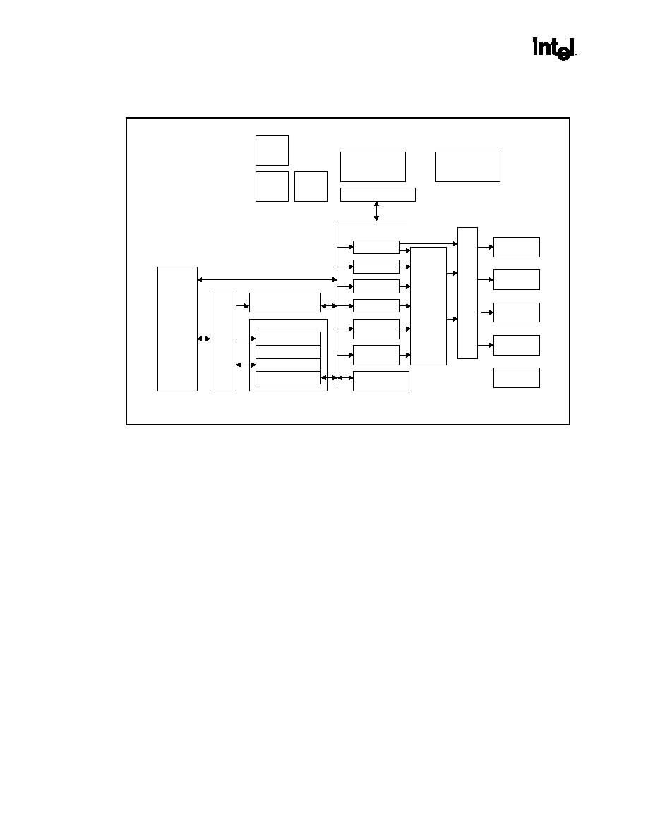
Intel
Æ
830 Chipset Family
158 Datasheet
298338-003
R
Figure 15. Intel 830M and 830MG Chipset GMCH-M Graphics Block Diagram
AGP 2.0
Interface
Instr./
Data
Setup/Transform
3D Engine
Scan Conversion
Texture Engine
Raster Engine
2D Engine
Overlay
Sprite
Cursor
Primary
Display
Secondary
Display
Motion
Compensation
Alpha
Blend/
Gamma/
Cursor
Cntl
Mux
Port
DAC
DVOA
DVOB
DVOC
DDC
Memory Control
Direct RDRAM
Clocks/Reset
Built-in
Scan
Power
Mgmt
GPIO
High bandwidth access to data is provided through the system memory port. The Intel 830M and
830MG Chipset GMCH-M can access UMA memory located in system memory at 1.06 GB/s. The Intel
830M and 830MG Chipset uses a tiling architecture to minimize page miss latencies and thus maximize
effective rendering bandwidth.
5.4.1 3D/2D
Instruction
Processing
The Intel 830M and 830MG GMCH-M contain an extensive set of instructions that control various
functions including 3D rendering, BLT operations, display, MPEG decode acceleration, and overlay.
The 3D instructions set 3D pipeline states and control the processing functions. The 2D instructions
provide an efficient method for invoking BLT operations.
5.4.2 3D
Engine
The 3D engine of the Intel 830M and 830MG Chipset GMCH-M has been designed with a deep
pipelined architecture, where performance is maximized by allowing each stage of the pipeline to
simultaneously operate on different primitives or portions of the same primitive. GMCH-M supports
Perspective-correct Texture Mapping, Multitextures, Bump-Mapping, Cubic Environment Maps,
Bilinear, Trilinear & Anisotropic MIP mapped filtering, Gouraud shading, Alpha-blending, Vertex and
Per Pixel Fog, and Z/W Buffering. These features are independently enabled (disabled) via a set of 3D
instructions.
The 3D pipeline subsystem performs the 3D rendering acceleration. The main blocks of the pipeline are
the Setup Engine, Scan Converter, Texture Pipeline, and Raster Pipeline. A typical programming

Intel
Æ
830 Chipset Family
298338-003 Datasheet
159
R
sequence would be to send instructions to set the state of the pipeline followed by rendering instructions
containing 3D primitive vertex data.
5.4.2.1 Setup
Engine
The Intel 830M and 830MG Chipset GMCH-M 3D setup engine takes the input data associated with
each vertex of a 3D primitive and computes the various parameters required for scan conversion. In
formatting this data, GMCH-M maintains sub-pixel accuracy. The per-vertex data is converted into
gradients that can be used to interpolate the data at any pixel within a polygon (colors, alpha, Z depth,
fog, and texture coordinates). The pixels covered by a polygon are identified and per-pixel texture
addresses are calculated.
5.4.2.2
Viewport Transform and Perspective Divide
The 3D-geometry pipeline involves transformation of vertices from model space to clipping space
followed by clip test and clipping. Lighting can be performed during the transformation or at any other
point in the pipeline. After clipping, the next stage involves perspective divide followed by
transformation to the viewport or screen space. The Intel 830M and 830MG Chipset GMCH-M can
support Viewport Transform and Perspective Divide portion of the 3D Geometry Pipeline in hardware.
5.4.2.3
3D Primitives and Data Formats Support
The 3D primitives rendered by the Intel 830M and 830MG Chipset GMCH-M are points, lines, discrete
triangles, line strips, triangle strips, triangle fans, and polygons. In addition to this, GMCH-M supports
DirectX6's Flexible Vertex Format (FVF), which enables the application to specify a variable length of
parameter list obviating the need for sending unused information to the hardware. Strips, Fans, and
Indexed Vertices as well as FVF improves delivered vertex rate to the setup engine significantly.
5.4.2.4
Pixel Accurate Fast Scissoring and Clipping Operation
The Intel 830M and 830MG Chipset GMCH-M supports clipping to a scissoring rectangle within the
drawing window. GMCH-M 's clipping and scissoring in hardware reduce the need for software to
process polygons, and thus improves performance. During the setup stage, GMCH-M clips polygons to
the drawing window. The scissor rectangle accelerates the clipping process by allowing the driver to clip
to a bigger region than the hardware renders to. The scissor rectangle needs to be pixel accurate, and
independent of line and point width. GMCH-M supports a single scissor box rectangle.
5.4.2.5 Backface
Culling
As part of the setup, the Intel 830M and 830MG Chipset GMCH-M discards polygons from further
processing, if they are facing away from or towards the user's viewpoint. This operation, referred to as
"Back Face Culling" is accomplished based on the "clockwise" or "counter-clockwise" orientation of the
vertices on a primitive. This can be enabled or disabled by the driver.
5.4.2.6 Scan
Converter
The Scan Converter takes the vertex and edge information is used to identify all pixels that are affected
by features being rendered. It works on a per-polygon basis, and one polygon may be entering the
pipeline while calculations finish on another.

Intel
Æ
830 Chipset Family
160 Datasheet
298338-003
R
5.4.2.7 Texture
Engine
As texture sizes increase beyond the bounds of graphics memory, executing textures from graphics
memory becomes impractical. The Intel 830M and MG Chipset GMCH-M, using Intel's Direct
Memory Execution model, simplifies this process by rendering each scene using the texture located in
system memory. The 830M and 830MG Chipsets include a cache controller to avoid frequent memory
fetches of recently used texture data.
The 830M and 830MG Chipsets allow an image, pattern, or video to be placed on the surface of a 3D
polygon. The texture engine performs texture color or chromakey matching, texture filtering
(anisotropic, trilinear, and bilinear interpolation), and YUV to RGB conversions.
5.4.2.8
Perspective Correct Texture Support
Textured polygon is generated by mapping a 2D texture pattern onto each pixel of the polygon. A texture
map is like wallpaper pasted onto the polygon. Since polygons are rendered in perspective, it is
important that texture be mapped in perspective as well. Without perspective correction, texture is
distorted when an object recedes into the distance. Perspective correction involves a compute-intensive
"per-pixel-divide" operation on each pixel. Perspective correction is necessary for realistic 3D graphics.
5.4.2.8.1 Texture
Decompression
DirectX7.0 supports Texture Compression to reduce the bandwidth required to deliver textures. As the
textures' average sizes (512x512) get larger with higher color depth and multiple textures become the
norm, it becomes increasingly important to provide a mechanism compress textures. The Intel 830M
and 830MG Chipset GMCH-M supports DX7 decompression. Texture decompression formats supported
include DXT1, DXT2, DXT3, DXT4, DXT5.
5.4.2.9
Texture ColorKey and ChromaKey
ColorKey and ChromaKey describe two methods of removing a specific color or range of colors from a
texture map before it is applied to an object. For "nearest" texture filter modes, removing a color simply
makes those portions of the object transparent (the previous contents of the back buffer show through).
For "linear" texture filtering modes, the texture filter is modified if only the non-nearest neighbor texels
match the key (range).
ColorKeying occurs with paletted textures and removes colors according to an index (before the palette
is accessed). When a color palette is used with indices to indicate a color in the palette, the indices can
be compared against a state variable "ColorKey Index Value" and if a match occurs and ColorKey is
enabled, then this value's contribution is removed from the resulting pixel color. The Intel 830M and
830MG Chipset GMCH-M defines index matching as ColorKey.
ChromaKeying can be performed for both paletted and non-paletted textures, and removes texels that
fall within a specified color range. The ChromaKey mode refers to testing the ARGB or YUV
components to see if they fall between high and low state variable values. If the color of a texel
contribution is in this range and chromakey is enabled, then this contribution is removed from the
resulting pixel color.
5.4.2.10 Anti-aliasing
Aliasing is one of the artifacts that degrade image quality. In its simplest manifestation, aliasing causes
the jagged staircase effects on sloped lines and polygon edges. Another artifact is the moirÈ patterns,
which occur as a result of the fact that there is very small number of pixels available on screen to contain
the data of a high-resolution texture map.

Intel
Æ
830 Chipset Family
298338-003 Datasheet
161
R
Full Scene Anti-Aliasing uses supersampling, which means that the image is rendered internally at a
higher resolution than it is displayed on screen. The Intel 830M and 830MG GMCH-M can render
internally at 1600x1200 and then this image is downsampled (via a Bilinear filter) to the screen
resolution of 640x480 and 800x600. Full Scene Anti-aliasing removes jaggies at the edges as well as
moirÈ patterns. The GMCH-M renders the supersampled image up to 2Kx2K pixel dimensions. The
GMCH-M then reads it as a texture and bilinear filters it to the final resolution.
5.4.2.11
Texture Map Filtering
Many texture-mapping modes are supported. Perspective correct mapping is always performed. As the
map is fitted across the polygon, the map can be tiled, mirrored in either the U or V directions, or
mapped up to the end of the texture and no longer placed on the object (this is known as clamp mode).
The way a texture is combined with other object attributes is also definable.
∑
830M/830MG GMCH-M supports up to 12 Levels-of-Detail (LODs) ranging in size from
2048x2048 to 1x1 texels. (A texel is defined as a texture map element). Included in the texture
processor is a texture cache, which provides efficient MIP-mapping.
∑
830M/830MG GMCH-M supports 7 types of texture filtering:
∑
Nearest (also known as Point Filtering): Texel with coordinates nearest to the desired pixel is used.
(This is used if only one LOD is present).
∑
Linear (also known as Bilinear Filtering): A weighted average of a 2x2 area of texels surrounding
the desired pixel are used. (This is used if only one LOD is present).
∑
Nearest MIP Nearest (also known as Point Filtering): This is used if many LODs are present. The
nearest LOD is chosen and the texel with coordinates nearest to the desired pixel are used.
∑
Linear MIP Nearest (Bilinear MIP Mapping): This is used if many LODs are present. The nearest
LOD is chosen and a weighted average of a 2x2 area of texels surrounding the desired pixel are
used (four texels). This is also referred to as Bilinear MIP Mapping.
∑
Nearest MIP Linear (Point MIP Mapping): This is used if many LODs are present. Two appropriate
LODs are selected and within each LOD the texel with coordinates nearest to the desired pixel are
selected. The Final texture value is generated by linear interpolation between the two texels selected
from each of the MIP Maps.
∑
Linear MIP Linear (Trilinear MIP Mapping): This is used if many LODs are present. Two
appropriate LODs are selected and a weighted average of a 2x2 area of texels surrounding the
desired pixel in each MIP Map is generated (four texels per MIP Map). The Final texture value is
generated by linear interpolation between the two texels generated for each of the MIP Maps.
Trilinear MIP Mapping is used minimize the visibility of LOD transitions across the polygon.
∑
Anisotropic MIP Nearest (Anisotropic Filtering): This is used if many LODs are present. The
nearest LOD-1 level will be determined for each of four sub-samples for the desired pixel. These
four sub-samples are then bilinear filtered and averaged together.
∑
Both D3D (DirectX 6.0) and OGL (Rev.1.1) allows support for all these filtering modes.
5.4.2.12
Multiple Texture Composition
830M/830MG GMCH-M also performs multiple texture composition. This allows the combination of
two or greater MIP maps to produce a new one with new LODs and texture attributes in a single or
iterated pass. The setup engine supports up to four texture map coordinates in as single pass. GMCH-M
allows up to two Bilinear MIP Maps or a single Trilinear MIP Map to be composited in a single pass.
Greater than two Bilinear MIP Maps or more than one Trilinear MIP Map would require multiple passes.

Intel
Æ
830 Chipset Family
162 Datasheet
298338-003
R
The actual blending or composition of the MIP Maps is done in the raster engine. The texture engine
provides the required texels including blending information.
Flexible vertex format support allows multi-texturing because it makes it possible to pass more than one
texture in the vertex structure.
5.4.2.13 Cubic
Environment
Mapping
Environment maps allow applications to render scenes with complex lighting and reflections while
significantly decreasing CPU load. There are several methods to generate environment maps such as
spherical, circular, and cubic. 830M/830MG GMCH-M has selected to support cubic reflection mapping
over spherical and circular since it is the best choice to provide real-time environment mapping for
complex lighting and reflections.
Cubic Mapping requires a texture map for each of the 6 cube faces. These can be generated by pointing
a camera with a 90-degree field-of-view in the appropriate direction. Per-vertex vectors (normal,
reflection or refraction) are interpolated across the polygon and the intersection of these vectors with the
cube texture faces is calculated. Texel values are then read from the intersection point on the appropriate
face and filtered accordingly.
5.4.2.14 Bump
Mapping
Bump mapping is a feature in the 830M/830MG GMCH-M that enables a surface to appear wrinkled or
dimpled without the need to model these depressions geometrically. By perturbing environment map
texture coordinates on a per pixel basis using delta values read from the bump map, non-uniform lighting
effects (reflections, etc.) can be applied. This can give flat objects a bumpy or raised appearance.
Embossing, a simpler form of bump mapping, is achieved by layering two identical texture maps. It can
be supported through software to give the appearance of depth.
5.4.3 Raster
Engine
The Raster Engine is where the color data such as fogging, specular RGB, texture map blending, etc. is
processed. The final color of the pixel is calculated and the RGBA value combined with the
corresponding components resulting from the Texture Engine. These textured pixels are modified by the
specular and fog parameters. These specular highlighted, fogged, textured pixels are color blended with
the existing values in the frame buffer. In parallel, stencil, alpha and depth buffer tests are conducted
which will determine whether the Frame and Depth Buffers will be updated with the new pixel values.
5.4.3.1
Texture Map Blending
Multiple Textures can be blended together in an iterative process and applied to a primitive.
830M/830MG GMCH-M allows up to four distinct or shared texture coordinates and texture maps to be
specified onto the same polygon. Also, GMCH-M supports using a texture coordinate set to access
multiple texture maps. State
variables in multiple texture are bound to texture coordinates, texture map
or texture blending.
5.4.3.2
Combining Intrinsic and Specular Color Components
The Intel 830M and 830MG GMCH-M allows an independently specified and interpolated "specular
RGB" attribute to be added to the post-texture blended pixel color. This feature provides a full RGB
specular highlight to be applied to a textured surface, permitting a high quality reflective colored lighting
effect not available in devices, which apply texture after the lighting components have been combined. If
specular-add state variable is disabled, only the resultant colors from the map blending are used. If this

Intel
Æ
830 Chipset Family
298338-003 Datasheet
163
R
state variable is enabled, RGB values from the output of the map blending are added to values for RS,
GS, BS on a component by component basis.
5.4.3.3
Color Shading Modes
The Raster Engine will support the flat and Gouraud shading modes. These shading modes are
programmed by the appropriate state variables issued through the command stream.
Flat shading is performed by smoothly interpolating the vertex intrinsic color components (Red, Green,
Blue), Specular (R,G,B), Fog, and Alpha to the pixel, where each vertex color has the same value. The
setup engine substitutes one of the vertex's attribute values for the other two vertices attribute values
thereby creating the correct flat shading terms. This condition is set up by the appropriate state variables
issued prior to rendering the primitive.
Gouraud shading is performed by smoothly interpolating the vertex intrinsic color components (Red,
Green, Blue). Specular (RGB), Fog, and Alpha to the pixel, where each vertex color has a different
value.
All the attributes can be selected independently to one of the shading mode by setting the appropriate
value state variables.
5.4.3.4 Color
Dithering
Color Dithering in the GMCH-M helps to hide color quantization errors. Color Dithering takes
advantage of the human eye's propensity to "average" the colors in a small area. Input color, alpha, and
fog components are converted from 8-bit components to 5-bit or 6- bit component by dithering.
Dithering is performed on blended textured pixels. In 32-bit mode, dithering is not performed on the
components
5.4.3.5
Vertex and Per Pixel Fogging
Fogging is used to create atmospheric effects such as low visibility conditions in flight simulator-type
games. It adds another level of realism to computer-generated scenes. Fog can be used for depth cueing
or hiding distant objects. With fog, distant objects can be rendered with fewer details (less polygons),
thereby improving the rendering speed or frame rate. Fog is simulated by attenuating the color of an
object with the fog color as a function of distance, and the greater the distance, the higher the density
(lower visibility for distant objects). There are two ways to implement the fogging technique: per-vertex
(linear) fogging and per-pixel (non-linear) fogging. The per-vertex method interpolates the fog value at
the vertices of a polygon to determine the fog factor at each pixel within the polygon. This method
provides realistic fogging as long as the polygons are small. With large polygons (such as a ground plane
depicting an airport runway), the per-vertex technique results in unnatural fogging
GMCH-M supports both types of fog operations, vertex and per pixel or table fog. If fog is disabled, the
incoming color intensities are passed unchanged to the destination blend unit.
If fog is enabled, the incoming pixel color is blended with the fog color based on a fog coefficient on a
per pixel basis using the following equation before sending to the destination blend unit.
5.4.3.6
Alpha Blending (Frame Buffer)
Alpha Blending in the Intel 830M and 830MG GMCH-M adds the material property of transparency or
opacity to an object. Alpha blending combines a source pixel color (RsGsBs) and alpha (As) component
with a destination pixel color (RdGdBd) and alpha(Ad) component. For example, this is so that a glass

Intel
Æ
830 Chipset Family
164 Datasheet
298338-003
R
surface on top (source) of a red surface (destination) would allow much of the red base color to show
through.
Blending allows the source and destination color values to be multiplied by programmable factors and
then combined via a programmable blend function. The combined and independent selection of factors
and blend functions for color and alpha is supported.
5.4.3.7
Color Buffer Formats: (Destination Alpha)
The Raster Engine will support 8-bit, 16-bit, and 32-bit Color Buffer Formats. The 8-bit format is used
to support planar YUV420 format, which used only in Motion Compensation and Arithmetic Stretch
format. The bit format of Color and Z will be allowed to mix.
The Intel 830M and 830MG GMCH-M will support an 8-bit destination alpha in 32-bit mode.
Destination alpha will be supported in 16-bit mode in 1555 or 4444 format.
GMCH-M does not support general 3D rendering to 8-bit surfaces. 8-bit destinations are supported for
operations on planar YUV surfaces (e.g., stretch Blts) where each 8-bit color component is written in a
separate pass. GMCH-M also supports a mode where both U and V planar surfaces can be operated on
simultaneously.
The frame buffer of GMCH-M contains at least two hardware buffers-the Front Buffer (display buffer)
and the Back Buffer (rendering buffer). While the back buffer may actually coincide with (or be part of)
the visible display surface, a separate (screen or window-sized) back buffer is
typically
used to permit
double-buffered drawing. That is, the image being drawn is not visible until the scene is complete and
the back buffer made visible or copied to the front buffer via a 2D BLT operation. Rendering to one
buffer and displaying from the other buffer removes image tearing artifacts. Additionally, more than
two back buffers (e.g., triple-buffering) can be supported.
5.4.3.8 Depth
Buffer
The Raster Engine will be able to read and write from this buffer and use the data in per fragment
operations that determine resultant color and depth value of the pixel for the fragment are to be updated
or not.
Typical applications for entertainment or visual simulations with exterior scenes require far/near ratios
of 1000 to 10000. At 1000, 98 percent of the range is spent on the first 2 percent of the depth. This can
cause hidden surface artifacts in distant objects, especially when using 16-bit depth buffers. A 24-bit Z-
buffer provides 16 million Z-values as opposed to only 64K with a 16-bit Z-buffer. With lower Z-
resolution, two distant overlapping objects may be assigned the same Z-value. As a result, the rendering
hardware may have a problem resolving the order of the objects, and the object in the back may appear
through the object in the front.
By contrast, when w (or eye-relative z) is used, the buffer bits can be more evenly allocated between the
near and far clip planes in world space. The key benefit is that the ratio of far and near is no longer an
issue, allowing applications to support a maximum range of miles, yet still get reasonably accurate depth
buffering within inches of the eye point. The selection of depth buffer size is relatively independent of
the color buffer. A 16 bit Z/W or 24 bit Z/W buffer can be selected with a 16-bit color buffer. Z buffer is
not supported in 8-bit mode.
5.4.3.9 Stencil
Buffer
The Raster Engine will provide 8-bit stencil buffer storage in 32-bit mode and the ability to perform
stencil testing. Stencil testing controls 3D drawing on a per pixel basis, which conditionally eliminates a

Intel
Æ
830 Chipset Family
298338-003 Datasheet
165
R
pixel on the outcome of a comparison between a stencil reference value and the value in the stencil
buffer at the location of the source pixel being processed. They are typically used in multipass
algorithms to achieve special effects, such as decals, outlining, shadows and constructive solid geometry
rendering.
One of three possible stencil operations is performed when stencil testing is enabled. The stencil
operation specifies how the stencil buffer is modified when a fragment passes or fails the stencil test.
The selection of the stencil operation to be performed is based upon the result of the stencil test and the
depth test. A stencil write mask is also included that controls the writing of particular bits into the stencil
buffer. It selects between the destination value and the updated value on a per-bit basis. The mask is 8-
bit wide.
5.4.3.10 Projective
Textures
830M/830MG GMCH-M will support two simultaneous projective textures at full rate processing. These
textures require 3 floating-point texture coordinates to be included in the FVF format. Projective
textures enable special effects such as projecting spot light textures obliquely onto walls, etc.
5.4.4 2D
Engine
The 830M and 830MG Chipset GMCH-M provide an extensive set of 2D instructions and 2D HW
acceleration for block transfers of data (BLTs). The BLT engine provides the ability to copy a source
block of data to a destination and perform operations (e.g., ROP1, ROP2, and ROP3) on the data using a
pattern, and/or another destination. The Stretch BLT engine is used to move source data to a destination
that need not be the same size, with source transparency. Performing
these common tasks in hardware
reduces CPU load, and thus improves performance.
5.4.4.1
GMCH-M VGA Registers and Enhancements
The 2D registers are a combination of registers defined by IBM* when the Video Graphics Array (VGA)
was first introduced and others that Intel has added to support graphics modes that have color depths,
resolutions, and hardware acceleration features that go beyond the original VGA standard.
5.4.4.2
256-Bit Pattern Fill and BLT Engine
Use of this BLT engine accelerates the Graphical User Interface (GUI) of Microsoft* Windows*. The
GMCH-M BLT Engine provides hardware acceleration of block transfers of pixel data for many
common Windows operations. The term BLT refers to a block transfer of pixel data between memory
locations. The BLT engine can be used for the following:
∑
Move rectangular blocks of data between memory locations
∑
Data Alignment
∑
Perform logical operations (raster ops)
The rectangular block of data does not change as it is transferred between memory locations. Data to be
transferred can consist of regions of memory, patterns, or solid color fills. A pattern will always be 8x8
pixels wide and may be 8, 16, or 32 bits per pixel.
The 830M/830MG GMCH-M BLT engine has the ability to expand monochrome data into a color depth
of 8, 16, or 32 bits. BLTs can be either opaque or transparent. Opaque transfers, move the data
specified to the destination. Transparent transfers compare destination color to source color and write
according to the mode of transparency selected.

Intel
Æ
830 Chipset Family
166 Datasheet
298338-003
R
Data is horizontally and vertically aligned at the destination. If the destination for the BLT overlaps with
the source memory location, GMCH-M can specify which area in memory to begin the BLT transfer.
Hardware is included for all 256 raster operations (Source, Pattern, and Destination) defined by
Microsoft, including transparent BLT.
GMCH-M has instructions to invoke BLT operations, permitting software to set up instruction buffers
and use batch processing as described in the Instruction Processing Section. GMCH-M can perform
hardware clipping during BLTs.
5.4.4.3 Alpha
Stretch
BLT
The stretch BLT function can stretch source data in the X and Y directions to a destination larger or
smaller than the source. Stretch BLT functionality expands a region of memory into a larger or smaller
region using replication and interpolation. The stretch BLT function also provides format conversion and
data alignment.
5.4.5 Planes
and
Engines
Intel 830M and 830MG GMCH display can be functionality delineated into: Planes and Engines (Pipes
and Ports). A plane consists of rectangular shaped image that has characteristics such as source, size,
position, method, and format. These planes get attached to source surfaces, which are rectangular
memory surfaces with a similar set of characteristics. They are also associated with a particular
destination pipe.
A pipe consists of a set of planes that will be combined and a timing generator. A port is the destination
for the result of the pipe. Therefore, planes are associated with pipes and pipes are associated with ports
.
5.4.5.1
Dual Display Functionality
The display consists of two display pipes. Pipes have a set of planes that are assigned to them as sources.
The analog display port is restricted to Pipe A, while any of the DVOs may use either Pipe A or Pipe B.
This limits the resolutions available on a digital display when an analog CRT is active. Please refer to
the Intel
Æ
830M PC10 Product Requirements (Please contact local Intel representative).

Intel
Æ
830 Chipset Family
298338-003 Datasheet
167
R
Table 38. Dual Display Usage Model
Display Pipe A
Display Pipe B
CRT LCD
CRT DVI
CRT TV
CRT LCD
(DVOB+DVOC)
CRT DVI
(DVOB+DVOC)
LCD TV
LCD DVI
(DVOB+DVOC)
LCD (DVOB+DVOC)
DVI
LCD (DVOB+DVOC)
TV
DVI TV
5.4.6 Hardware
Cursor
Plane
The Intel 830M and 830MG Chipsets support two hardware cursors. The cursor plane is one of the
simplest display planes. With a few exceptions, has a fixed size of 64x64 and a fixed Z-order (top). In
legacy modes, cursor can cause the display data below it to be inverted. In the alpha blend mode, true
color cursor data can be alpha blended into the display stream. It can be assigned to either display pipe
A or display pipe B and dynamically flipped from one to the other when both are running.
5.4.6.1
Cursor Color Formats
Color data can be in an indexed format or a true color format. Indexed data uses the entries in the four-
entry cursor palette to convert the two-bit index to a true color format before being passed to the
blenders. The index can optionally specify that a cursor pixel be transparent or cause an inversion of the
pixel value below it or one of two colors from the cursor palette. Blending of YUV or RGB data is only
supported with planes that have data of the same format.
5.4.6.2
Cursor Hot Spot
There is the additional function of defining a cursor hot spot. This hot spot is the pixel that is positioned
over the user selection. This is accomplished by allowing negative XY offset values and ones that
exceed the size of the underlying active region and trimming the excess display data.
5.4.6.3 Popup
Plane
The popup plane is used for control functions in mobile applications. This is not used for typical
desktop applications. Only the hardware cursor has a higher Z-order precedence over the hardware icon.
In standard modes (non-VGA) either cursor A or cursor B can be used as a Popup Icon. For VGA
modes, 32-bpp data format is not supported.

Intel
Æ
830 Chipset Family
168 Datasheet
298338-003
R
5.4.6.4
Popup Color Formats
Source color data for the popup is in an indexed format. Indexed data uses the entries in the four-entry
cursor palette to convert the two-bit index to a true color format before being passed to the blenders.
Blending of color data is only supported with data of the same format.
5.4.7 Overlay
Plane
The overlay engine provides a method of merging either video capture data (from an external Video
Capture device) or data delivered by the CPU, with the graphics data on the screen.
5.4.7.1 Multiple
Overlays
A single overlay plane and scalar is implemented. This overlay plane can be connected to the primary
display, secondary display or in bypass mode. In the default mode, it appears on the primary display.
The overlay may be displayed in a multi-monitor scenario for single-pipe simultaneous displays only.
Picture-in-Picture Feature is supported via software through the arithmetic stretch blitter.
5.4.7.2 Source/Destination
Color-/Chroma-Keying
Overlay source/destination chroma-keying enables blending of the overlay with the underlying graphics
background. Destination color-/chroma-keying can be used to handle occluded portions of the overlay
window on a pixel-by-pixel basis that is actually an underlay. Destination color keying supports a
specific color (8 or 15 bit) mode as well as 32 bit alpha blending.
Source color-/chroma-keying is used to handle transparency based on the overlay window on a pixel-by-
pixel basis. This is used when "blue screening" an image to overlay the image on a new background
later.
5.4.7.3 Gamma
Correction
To compensate for overlay color intensity loss, the overlay engine supports independent gamma
correction. This allows the overlay data to be converted to linear data or corrected for the display device
when not blending.
5.4.7.4
YUV to RGB Conversion
The format conversion can be bypassed in the case of RGB source data.
5.4.7.5 Color
Control
Color control provides a method of changing the color characteristics of the pixel data. It is applied to
the data while in YUV format and uses input parameters such as brightness, saturation, hue (tint) and
contrast. This feature is supplied for the overlay only and works in YUV formats only.
5.4.7.6 X/Y
Mirroring
Both X or Y mirroring in the overlay is supported for video conferencing applications
.

Intel
Æ
830 Chipset Family
298338-003 Datasheet
169
R
5.4.7.7
Dynamic Bob and Weave
Interlaced data that originates from a video camera creates two fields that are temporally offset by 1/60
of a second. There are several schemes to de-interlace the video stream: line replication, vertical
filtering, field merging and vertical temporal filtering. Field merging takes lines from the previous field
and inserts them into the current field to construct the frame ≠ this is known as Weaving. This is the best
solution for images with little motion; however, showing a frame that consists of the two fields will have
serration or feathering of moving edges when there is motion in the scene. Vertical filtering or "Bob"
interpolates adjacent lines rather replicating the nearest neighbor. This is the best solution for images
with motion however, it will have reduced spatial resolution in areas that have no motion and introduces
jaggies. In absence of any other de-interlacing, these form the baseline and are supported by Intel 830 M
and MG Chipset GMCH-M.
5.4.8 Video
Functionality
5.4.8.1 MPEG-2
Decoding
GMCH-M MPEG2 Decoding supports Hardware Motion Compensation (MC).
GMCH-M can accelerate video decoding for the following video coding standards:
∑
MPEG-2: Full feature support
∑
MPEG-1: Full feature support
∑
H.261: Full feature support
∑
H.263: Full feature support
∑
H.263+: Most of features with some exceptions of H.263+ optional features
∑
MPEG-4: Only supports some features in the simple profile.
The Intel 830M and 830MG Chipset HWMC interface is optimized for Microsoft's VA API. Hardware
Video Acceleration API (HVA) is a generic DirectDraw and DirectShow interface supported in
Windows 2000 and Windows 98 Millennium to provide video decoding acceleration. Direct VA is the
open standard implementation of HVA, which is natively supported by the Intel 830M and 830MG
Chipset's hardware.
5.4.8.2
Hardware Motion Compensation
The Motion Compensation (MC) process consists of reconstructing a new picture by predicting (either
forward, backward, or bi-directional) the resulting pixel colors from one or more reference pictures. The
Intel 830M and 830MG
GMCH-M receives the video stream and implements Motion Compensation and
subsequent steps in hardware. Performing Motion Compensation in hardware reduces the processor
demand of software-based MPEG-2 decoding, and thus improves system performance.
5.5
Intel 830M and 830MG Chipset Internal Graphics
Display Interface
830M/830MG GMCH-M has two dedicated display ports, the analog port and digital display port A
(DVOA). Digital display port B (DVOB) and port C (DVOC) are multiplexed with the AGP interface
and are compromised if an external AGP graphics device is in use. Examples of this are TV encoders,
external DACs, LVDS transmitters, and TMDS transmitters. Each display port has control signals that

Intel
Æ
830 Chipset Family
170 Datasheet
298338-003
R
may be used to control, configure and/or determine the capabilities of an external device. The data that is
sent out the display port is selected from one of the two possible sources; display pipe A or display pipe
B. DVOB & DVOC can also operate in a "gang" mode, where the data bus is connected to both display
ports, allowing a single device to take data at twice the pixel rate.
GMCH-M's digital display ports are capable of driving a 165-MHz pixel clock. When in dual channel
mode (DVOB + DVOC), GMCH-M can be configured in gang mode to drive larger digital displays.
The Intel 830M and 830MG Chipset has three digital interfaces through display port (DVOA, DVOB,
and DVOC). Each interface is capable of driving a 165-MHz pixel clocks up to 165 MHz. The DVO
interface can support a variety of TV encoders, external DACs, LVDS transmitters, and TMDS
transmitters. Each display port has control signals that may be used to control, configure and/or
determine the capabilities of an external device. The data that is sent out the display port is selected from
one of the two possible sources; display pipe A or display pipe B. DVOB & DVOC can also operate in
a "gang" mode, where the data bus is connected to both display ports, allowing a single device to take
data at twice the pixel rate. When in dual channel mode (DVOB + DVOC), GMCH-M can be
configured in gang mode to drive larger digital displays.
In addition, the Intel 830M Chipset can also support a discrete AGP graphics device by multiplexing an
AGP interface with the DVOB and DVOC interfaces.
5.5.1
Analog Display Port Characteristics
The analog display port provides a RGB signal output along with a HSYNC and VSYNC signal. There
is an associated DDC signal pair that is implemented using GPIO pins dedicated to the analog port. The
intended target device is for a CRT based monitor with a VGA connector.
5.5.1.1 Integrated
RAMDAC
The display function contains a RAM-based Digital-to-Analog Converter (RAMDAC) that transforms
the digital data from the graphics and video subsystems to analog data for the CRT monitor. Three 8-bit
DACs provide the R, G, and B signals to the monitor.
5.5.1.2
DDC (Display Data Channel)
DDC is defined by VESA. Its purpose is to allow communication between the host system and display.
Both configuration and control information can be exchanged allowing plug-and-play systems to be
realized. Support for DDC 1 and 2 is implemented.
5.5.2
DVO Display Interface
The Intel 830M and MG GMCH-M has several options for driving digital displays. The Intel 830M and
830MG Chipset GMCH-M contains a dedicated digital display channel that can support DVO devices.
The Intel 830M Chipset also has two digital display channels that are multiplexed on the AGP interface.
When an external AGP graphics accelerator is not present, the Intel 830M Chipset can use the
multiplexed DVOs to provide extra DVO display options.
5.5.2.1
Dedicated Digital Display Channel - DVOA
The Intel 830M and 830MG GMCH-M has a dedicated port for digital display support. It will consist of
a 12-bit digital data bus with accompanying clocks and control signals. Please refer to Section 3.6.1 for
a detailed description of these signals. This port utilizes a 1.5-V interface for high speed signaling,

Intel
Æ
830 Chipset Family
298338-003 Datasheet
171
R
supporting a pixel clock up to 165 MHz. The port is designed to connect to a transmission device
capable of TMDS or TV-Out type signaling. For more details on the functionality of this interface,
please refer to the latest DVO specification.
5.5.2.2
Multiplexed Digital Display Channels ≠ DVOB and DVOC
The Intel 830M GMCH-M also has the capability to support additional digital display devices through
two digital visual ports muxed with the AGP signals. When an external graphics accelerator is utilized
via AGP, these digital display capabilities are compromised. The two multiplexed DVOs are very
similar to the dedicated DVO.
The muxed DVOs each support a pixel clock up to 165 MHz and can support a variety of transmission
devices. When using a 24-bit external transmitter, it will be possible to pair the two DVOs to support a
single digital display with higher resolutions and refresh rates.
5.5.2.2.1
Optional High Speed (Dual Channel) Interface
The multiplexed digital display ports can operate in either two 12-bit port mode or a single 24-bit mode.
The 24-bit mode uses the 12-bit DVOB data pins combined with the DVOC data pins to make a 24-bit
bus. This doubles the transfer rate capabilities of the port. In the single port case, horizontal periods
have a granularity of a single pixel clock; in the double case horizontal periods have a granularity of two
pixel clocks. In both cases, data is transferred on both edges of the differential clock.
5.5.2.3
DDC (Display Data Channel)
The dedicated digital display interface (DVOA) uses the DDC2_CLK/DDC2_DATA or I2C_CLK
/I2C_DATA to interrogate the panel. GMCH-M supports the DDC2B protocol to initiate the transfer of
EDID information. The dedicated digital display interface uses the I2C bus to interrogate the external
transmitter.
The multiplexed digital display interface (DVOB & DVOC) uses the M_I2C_CLK/M_I2C_DATA or
M_DDC1_CLK/M_DDC1_DATA to interrogate the panel. GMCH-M supports the DDC2B protocol to
initiate the transfer of EDID data. The multiplexed digital display interface uses the M_I2C bus to
interrogate the external transmitter.
5.5.2.4
Third Party TMDS/LVDS Support Capabilities
The Intel 830M and 830MG Chipset GMCH-M is compliant with the DVI Specification 1.0. When
combined with a DVI compliant device, the GMCH-M DVO port can drive a flat panel or a digital CRT.
5.5.2.5
TV Encoder Capabilities
The Intel 830M and 830MG Chipset GMCH-M supports TV encoders through the digital video output
(DVO) interface. GMCH-M will generate the proper timing for the external encoder. The external
encoder is responsible for generation of the proper format signal. Since the GMCH-M DVO interface is
1.5 V, care should be taken to ensure that the TV encoder is operational at that signaling voltage.
The TV-out interface on GMCH-M is addressable as a master device. This allows an external TV
encoder device to drive a pixel clock signal on DVOx_CLKIN that the Intel 830M and 830MG Chipset
will use as a reference frequency. The frequency of this clock is dependent on the output resolution
required. Data is driven to the encoder across 12 data lines, along with clock pair and sync signals. The
encoder can expect a continuous flow of data from GMCH-M because data will not be throttled.

Intel
Æ
830 Chipset Family
172 Datasheet
298338-003
R
5.5.2.5.1
Flicker Filter and Overscan Compensation
Overscan compensation scaling and the flicker filter is done in the external TV encoder chip. Care must
be taken to allow for support of TV sets with high performance de-interlacers and progressive scan
displays connected to by way of a non-interlaced signal. Timing will be generated with pixel granularity
to allow more overscan ratios to be supported.
5.5.2.5.2
Direct YUV From Overlay
When source material is in the YUV format and is destined for a device that can take YUV format data
in, it is desired to send the data without converting it to RGB. This avoids the truncation errors
associated with multiple color conversion steps. The common situation will be that the overlay source
data is in the YUV format and will bypass the conversion to RBG as it is sent to the TV port directly.
5.5.2.5.3
Analog Content Protection
Analog content protection will be provided through the external encoder using Macrovision 7.01. DVD
software must verify the presence of a Macrovision TV encoder before playback continues. Simple
attempts to disable the Macrovision operation must be detected.
5.5.2.5.4
Support of Progressive Scan SDTV TVs
Support will be included for progressive scan TV devices through the TV port. This support will include
the resolutions of 480p and 1080i using both a YUV analog signal with sync on Y and a RGB HV
connection for TVs with that connection.
Table 39. DVO Usage Model
DVOA DVOB DVOC
LCD DVI TV
LCD TV DVI
LCD
DVI or TV
DVI (DVOB+DVOC)
LCD (DVOB+DVOC)
DVI or TV
LCD
DVI or TV
DVI or TV
DVI or TV
LCD
The Intel 830M and 830MG Chipset GMCH-M do not support two TV encoders devices at a time
.
5.5.3
Concurrent and Simultaneous Display
The Intel 830M and 830MG Chipset GMCH-M has two independent pipes, each with its own timing
generator and dot clock, and thus is able to support two displays concurrently. Windows* 98 and
Windows* 2000 have enabled support for multi-monitor display. There are two types of multi-monitor
solutions: Concurrent and Simultaneous. Concurrent displays different data on two screens whereas
Simultaneous displays the same information on both displays. The GMCH-M also supports a
combination of concurrent and simultaneous displays.
Intel
Æ
830 Chipset Family
298338-003 Datasheet
173
R
5.6
Intel 830M and 830MP Discrete AGP Interface
The 830M and 830MP Chipset will support 1.5-V AGP 1x/2x/4x devices. The AGP signal buffers will
have one mode of operation; 1.5-V drive/receive (not 3.3-V tolerant). The GMCH-M will support 4x
(266MT/s) clocking transfers for read and write data, and sideband addressing. The GMCH-M has a 32-
deep AGP request queue. The GMCH-M integrates a fully associative 16 entry Translation Look-aside
Buffer.
AGP semantic transactions to system SDRAM do not get snooped and are therefore not coherent with
the CPU caches. PCI semantic transactions on AGP to system SDRAM are snooped. AGP semantic
accesses to hub interface/PCI are not supported. PCI semantic access from an AGP master to hub
interface is not supported.
5.6.1
AGP Target Operations
As an initiator, the 830M and 830MP GMCH-M does not initiate cycles using AGP enhanced protocols.
The GMCH-M supports AGP target interface to main memory only. The GMCH-M supports interleaved
AGP and PCI transactions.
The following table summarizes target operation support of GMCH-M for AGP masters.
Table 40. AGP Commands Supported by GMCH-M When Acting as an AGP Target
AGP Command
C/BE[3:0]#
GMCH-M Host Bridge
Encoding
Cycle Destination
Response as AGP Target
Read
0000
Main Memory
Low Priority Read
0000
Hub interface
Complete with random data
Hi-Priority Read
0001
Main Memory
High Priority Read
0000
hub interface
Complete with random data
Reserved 0010
N/A
No
Response
Reserved 0011
N/A
No
Response
Write 0100
Main
Memory
Low
Priority
Write
0100
hub interface
Cycle goes to SDRAM with BE's inactive
Hi-Priority Write
0101
Main Memory
High Priority Write
0101
hub interface
Cycle goes to SDRAM with BE's inactive
- does not go to hub interface
Reserved 0110
N/A
No
Response
Reserved 0111
N/A
No
Response
Long Read
1000
Main Memory
Low Priority Read
Hub interface
Complete locally with random data -
does not go to hub interface
Hi-Priority Long Read
1001
Main Memory
High Priority Read
Hub interface
Complete with random data
Flush
1010
GMCH-M
Complete with QW of Random Data
Reserved 1011
N/A
No
Response

Intel
Æ
830 Chipset Family
174 Datasheet
298338-003
R
Fence
1100
GMCH-M
No Response ≠ Flag inserted in GMCH-
M request queue
Reserved 1101
N/A
No
Response
Reserved 1110
N/A
No
Response
Reserved 1111
N/A
No
Response
NOTE: N/A refers to a function that is not applicable.
As a target of an AGP cycle, the GMCH-M supports all the transactions targeted at main memory and
summarized in the table above. The GMCH-M supports both normal and high priority read and write
requests. The GMCH-M will not support AGP cycles to hub interface. AGP cycles do not require
coherency management and all AGP initiator accesses to main memory using AGP protocol are treated
as non-snoopable cycles. These accesses are directed to the AGP aperture in main memory that is
programmed as either uncacheable (UC) memory or write combining (WC) in the processor's MTRRs.
5.6.2 AGP
Transaction
Ordering
The Intel 830M and 830MP Chipset GMCH-M observes transaction ordering rules as defined by the
AGP 2.0 specification.
5.6.3 AGP
Electricals
4x/2x/1x and PCI data transfers use 1.5V signaling levels as described in the AGP 2.0 specification.
5.6.4
Support for PCI-66 Devices
The Intel 830M and 830MP Chipset GMCH-M's AGP interface may be used as a PCI-66 MHz interface
with the following restrictions:
∑
Support for 1.5-V operation only.
∑
Support for only one device. GMCH-M will not provide arbitration or electrical support for more
than one PCI-66 device.
∑
The PCI-66 device must meet the AGP 2.0 electrical specification.
∑
The GMCH-M does not provide full PCI-to-PCI bridge support between AGP/PCI and hub
interface. Traffic between AGP and hub interface is limited to hub interface-to-AGP memory
writes.
∑
LOCK# signal is not present. Neither inbound nor outbound locks are supported.
∑
SERR#/PERR# signals are not present.
∑
16-clock Subsequent Data Latency timer (instead of 8)
5.6.5 4x
AGP
Protocol
In addition to the 1x and 2x AGP protocol the Intel 830M and 830MP GMCH-M supports 4x AGP read
and write data transfers, and 4x sideband address generation. 4x operation will be compliant with the 4x
AGP spec as currently described in AGP 2.0.
The 4x data transfer protocol provides 1.06 GB/s transfer rates. The control signal protocol for the 4x
data transfer protocol is identical to 1x/2x protocol. In 4x mode 16 bytes of data are transferred during

Intel
Æ
830 Chipset Family
298338-003 Datasheet
175
R
each 66-MHz clock period. The minimum throttle-able block size remains four 66-MHz clocks which
means 64 bytes of data is transferred per block. Three additional signal pins are required to implement
the 4x data transfer protocol. These signal pins are complementary data transfer strobes for the AD bus
(2) and the SBA bus (1).
5.6.6 Fast
Writes
The Fast Write (FW) transaction is from the core logic to the AGP master acting as a PCI target. This
type of access is required to pass data/control directly to the AGP master instead of placing the data into
main memory and then having the AGP master read the data. For 1x transactions, the protocol simply
follows the PCI bus specification. However, for higher speed transactions (2x or 4x), FW transactions
will follow a combination for PCI and AGP bus protocols for data movement.
5.6.7
AGP-to-Memory Read Coherency Mechanism
The Global Write Buffer (GWB) in the Intel 830MPand 830M Chipset is used to post write data from
the CPU, AGP/PCI, and hub interfaces prior to the data actually being written to system SDRAM. Reads
to system SDRAM are allowed to pass writes in the GWB. This policy requires that all reads to SDRAM
be checked against the writes in the GWB to maintain data coherency. If an AGP read hits a write in the
GWB, that particular write in the GWB and all writes queued in front of it are written to SDRAM prior
to the read. After the data hit by the AGP read is written to SDRAM the AGP read cycle is generated to
the SDRAM.
5.6.8
PCI Semantic Transactions on AGP
The Intel 830M and 830MP Chipset GMCH-M accepts and generates PCI semantic transactions on the
AGP bus. The GMCH-M guarantees that PCI semantic accesses to SDRAM are kept coherent with the
CPU caches by generating snoops to the CPU bus.
5.6.8.1
PCI Read Snoop-Ahead and Buffering
The Intel 830M and 830MP Chipset GMCH-M issues snoops dynamically for the various types of
memory read transactions and retains the contents of the AGP/PCI-to-SDRAM read buffers between
AGP/PCI transactions.
For Memory Reads the GMCH-M will issue one snoop and the entire cache line of read data will be
buffered. If a Memory Read bursts across the cache line, another snoop will be issued. Subsequent
Memory Read transaction hitting the cache line buffer will return data from the buffer.
For Memory Read Line and Memory Read Multiple the GMCH-M issues two snoops (a snoop followed
by a snoop-ahead) on the host bus and releases the CPU bus for other traffic. When the first DW of the
first cache line is delivered and FRAME# is still asserted, the GMCH-M will issue another snoop-ahead
on the host bus. This allows the GMCH-M to continuously supply data during Memory Read Line and
Memory Read Multiple bursts. When the transaction terminates there may be a minimum of 2 cache
lines and a maximum of 2 cache line plus 7 Dwords buffered. Subsequent Memory Reads hitting the
buffers will return data from the buffer.
5.6.8.2
Intel 830M and 830MP Chipset GMCH-M Initiator and Target Operations
The following table summarizes target operation support of the Intel 830M and 830MP Chipset GMCH-
M for AGP/PCI1 bus initiators. The cycles can be destined to either main memory or the hub interface
bus.

Intel
Æ
830 Chipset Family
176 Datasheet
298338-003
R
Table 41. PCI Commands Supported by GMCH-M When Acting as a PCI Target
PCI Command
C/BE[3:0]# Encoding
GMCH-M
Cycle Destination
Response as PCI Target
Interrupt Acknowledge
0000
N/A
No Response
Special Cycle
0001
N/A
No Response
I/O Read
0010
N/A
No Response
I/O Write
0011
N/A
No Response
Reserved 0100
N/A
No
Response
Reserved 0101
N/A
No
Response
Memory Read
0110
Main Memory
Read
0110
hub
interface
No
Response
Memory Write
0111
Main Memory
Posts Data
0111
hub
interface
No
Response
Reserved 1000
N/A
No
Response
Reserved 1001
N/A
No
Response
Configuration Read
1010
N/A
No Response
Configuration Write
1011
N/A
No Response
Memory Read Multiple
1100
Main Memory
Read
1100
hub
interface
No
Response
Dual Address Cycle
1101
N/A
No Response
Memory Read Line
1110
Main Memory
Read
1110
hub
interface
No
Response
Memory Write and Invalidate
1111
Main Memory
Posts Data
1111
hub
interface
No
Response
NOTE: N/A refers to a function that is not applicable.
As a target of an AGP/PCI cycle, GMCH-M only supports the following transactions:
Memory Read - The GMCH-M will issue one snoop and the entire cache line of read data will be
buffered. If a Memory Read bursts across the cache line another snoop will be issued but the
transaction will be disconnected on the cache line boundary. Subsequent Memory Read
transaction hitting the cache line buffer will return data from the buffer.
Memory Read Line, and Memory Read Multiple - These commands are supported identically by the
GMCH-M. The GMCH-M issues two snoops (a snoop followed by a snoop-ahead) on the
host bus and releases the CPU bus for other traffic. When the first DW of the first cache line
is delivered and FRAME# is still asserted, the GMCH-M will issue another snoop-ahead on
the host bus. This allows the GMCH-M to continuously supply data during Memory Read
Line and Memory Read Multiple bursts. When the transaction terminates there may be a
minimum of 2 cache lines and a maximum of 2 cache line plus 7 Dwords buffered.
Subsequent Memory Reads hitting the buffers will return data from the buffer.
Memory Write and Memory Write and Invalidate - These commands are aliased and processed
identically. The GMCH-M supports data streaming for PCI-to-SDRAM writes based on its

Intel
Æ
830 Chipset Family
298338-003 Datasheet
177
R
ability to buffer up to 128 bytes (16 Qwords) of data before a snoop cycle must be completed
on the host bus. The GMCH-M is typically able to support longer write bursts, with the
maximum length dependent upon concurrent host bus traffic during PCI-SDRAM write data
streaming.
Fast Back-to-Back Transactions - GMCH-M as a target supports fast back-to-back cycles from a PCI
initiator.
As a PCI initiator the GMCH-M is responsible for translating host cycles to AGP/PCI1 cycles. The
GMCH-M also transfers hub interface to AGP/PCI1 write cycles. The following table shows all the
cycles that need to be translated.

Intel
Æ
830 Chipset Family
178 Datasheet
298338-003
R
Table 42. PCI Commands Supported by GMCH-M When Acting as an AGP/PCI1 Initiator
GMCH-M Host Bridge
Source Bus
Command
Other Encoded Information
Corresponding
PCI1 Command
C/BE[3:0]#
Encoding
Source Bus: Host
Deferred Reply
Don't Care
None
N/A
Interrupt Acknowledge
Length
8 Bytes
None
N/A
Special Cycle
Shutdown
None
N/A
Halt
None
N/A
Stop Clock Grant
None
N/A
All
other
combinations
None
N/A
Branch Trace Message
None
None
N/A
I/O Read
Length
8 Bytes up to 4 Bex
asserted
I/O Read
0010
I/O Write
Length
8 Bytes up to 4 Bex
asserted
I/O Write
0011
I/O Read to 0CFCh
Length
8 Bytes up to 4 Bex
asserted
Configuration Read
1010
I/O Write to 0CFCh
Length
8 Bytes up to 4 Bex
asserted
Configuration Write
1011
Length
<
8 Bytes without all Bes
asserted
Memory Read
0110
Memory Read (Code or
Data)
Length
=
8 Bytes with all Bes
asserted
Memory Read
1110
Memory Read Invalidate
Length
=
16 Bytes
None
N/A
Length = 32 Bytes Code Only
Memory Read
1110
Length
<
8 Bytes without all Bes
asserted
Memory Write
0111
Memory Write
Length
=
16 Bytes
None
N/A
Length = 32 Bytes
Memory Write
0111
Locked Access
All combinations
Unlocked Access
1
As
Applicable
Reserved Encodings
All Combinations
None
N/A
EA Memory Access
Address
4 GB
None
N/A
Source Bus: hub interface
Memory Write
-
Memory Write
0111
NOTES:
1. CPU to AGP/PCI1 bus can result in deadlocks. Locked access to AGP/PCI1 bus is strongly discouraged
2. N/A refers to a function that is not applicable. Not Supported refers to a function that is available but specifically
not implemented on GMCH-M.

Intel
Æ
830 Chipset Family
298338-003 Datasheet
179
R
As an initiator of AGP/PCI1 cycle, the GMCH-M only supports the following transactions:
Memory Read - All CPU to AGP/PCI1 reads will use the Memory Read command.
Memory Write - GMCH-M initiates AGP/PCI1 cycles on behalf of the CPU or hub interface. GMCH-
M does not issue Memory Write and Invalidate as an initiator. GMCH-M does not support
write merging or write collapsing. GMCH-M will combine CPU-to-PCI writes (Dword or
Qword) to provide bursting on the AGP/PCI1 bus. GMCH-M allows non-snoopable write
transactions from hub interface to the AGP/PCI1 bus.
I/O Read and Write - I/O read and write from the CPU are sent to the AGP/PCI1 bus. I/O base and
limit address range for PCI1 bus are programmed in AGP/PCI1 configuration registers. All
other accesses that do not correspond to this programmed address range are forwarded to hub
interface.
Exclusive Access - GMCH-M will not issue a locked cycle on AGP/PCI1 bus on the behalf of either
the CPU or hub interface. Hub interface and CPU locked transactions to AGP/PCI1 will be
initiated as unlocked transactions by the GMCH-M on the AGP/PCI1 bus.
Configuration Read and Write - Host Configuration accesses to internal GMCH-M registers are
driven onto AGP/PCI1 as Type 1 Configuration Cycles where they are then claimed by the
GMCH-M. This is done to support co-pilot mode. Host Configuration cycles to AGP/PCI1
are forwarded as Type 1 Configuration Cycles.
5.6.8.3
GMCH-M Retry/Disconnect Conditions
The Intel 830M and 830MP GMCH-M generates retry/disconnect according to the AGP Specification
rules when being accessed as a target from the AGP interface (using PCI semantics).
5.6.8.4 Delayed
Transaction
When an AGP/PCI-to-SDRAM read cycle is retried by the GMCH-M it will be processed internally as a
Delayed Transaction.
The Intel 830M and 830MP GMCH-M supports the Delayed Transaction mechanism on the AGP target
interface for the transactions issued using PCI semantics. This mechanism is compatible with the PCI
2.2 Specification. The process of latching all information required to complete the transaction,
terminating with Retry, and completing the request without holding the master in wait-states is called a
Delayed Transaction. The GMCH-M latches the Address and Command when establishing a Delayed
Transaction. The GMCH-M generates a Delayed Transaction on the AGP only for SDRAM read
accesses.
5.7
Intel 830 Chipset Family GMCH-M Power and Thermal
Management
The following list provides the GMCH-M Power and Thermal Management Features:
∑
ACPI 1.0b & 2.0 support
∑
Mobile Power Reduction operating modes (C3, S1)
∑
System States: S0, S1, S3, S4, S5
∑
CPU States: C0, C1, C2, C3

Intel
Æ
830 Chipset Family
180 Datasheet
298338-003
R
∑
Graphics States: D0, D1, D3
∑
Compatible with Intel 815EM AGP Busy/Stop protocol
∑
Enhanced Intel SpeedStep
technology support
∑
Thermal Throttling for Main memory, and Graphics
5.7.1
ACPI 2.0 Support
Advanced Configuration and Power Management Interface (ACPI) primarily describes and runs
motherboard devices. It is completely controlled by the operating system that OS drivers directly power
down PCI/AGP devices. System or SMI BIOS plays a part of waking the system, however. Device
drivers save and restore state while bus drivers change the physical power state of the device.
The Intel 830 Chipset family GMCH-M power management architecture is designed to allow single
systems to support multiple suspend modes and to switch between those modes as required. A
suspended system can be resumed via a number of different events. The system returns to full operation
where it can continue processing or be placed into another suspend mode (potentially a lower power
mode than it resumed from).
GMCH-M supports the minimum requirements for ACPI support. GMCH-M must support the minimum
requirements for both system logic and for graphics controllers, as well as be capable of controlling
monitors minimum functions. The transition sequences of entering and exiting system, CPU and
graphics states are described in respective sections below.
5.7.2
ACPI States Supported
5.7.2.1
Intel 830M and 830MP Chipset ACPI Supported States
When a discrete AGP interface is used, the Intel 830M and 830MP Chipset supports the following ACPI
states:
1. System
States
G0/S0 Full
On
G1/S1 Power On Suspend (POS). System Context Preserved.
G1/S3 Suspend to RAM (STR). Power and context lost to Chipset.
G1/S4 Suspend to Disk (STD). All power lost (except wakeup on ICH3-M)
G2/S5 Hard off. Total reboot.
2.
CPU States
C0
Full
On
C1
Auto
Halt
C2
Quick Start
C3
Deep Sleep. Clock to CPU stopped Clock to CPU stopped or CPU DPSLP#
pin asserted

Intel
Æ
830 Chipset Family
298338-003 Datasheet
181
R
5.7.2.2
Intel 830M and 830MG Chipset ACPI Supported States
When internal graphics device is used, the Intel 830M and 830MG Chipset support the following ACPI
States:
1. System
States
G0/S0 Full
On
G1/S1 Power On Suspend (POS). System Context Preserved.
G1/S3 Suspend to RAM (STR). Power and context lost to Chipset.
G1/S4 Suspend to Disk (STD). All power lost (except wakeup on ICH3-M)
G2/S5 Hard off. Total reboot.
2.
CPU States
C0
Full
On
C1
Auto
Halt
C2
Quick Start
C3
Deep Sleep. Clock to CPU stopped Clock to CPU stopped or CPU DPSLP#
pin asserted
3.
Internal Graphics (IGD) States:
D0
Full on, display active
D1
Low power state, low latency recovery.
D3Hot
All state lost other than PCI configuration. Memory lost (optionally).
D3Cold
Power off

Intel
Æ
830 Chipset Family
182 Datasheet
298338-003
R
5.7.3
Intel 830 Chipset Family System and CPU States
Table 43 shows the state combinations that the Intel 830 Chipset family supports.
Table 43. Intel 830 Chipset Family System and CPU States
Global (G) State
Sleep (S) State
CPU (C) State
Processor State
Description
G0 S0 C0 Full
On
Full
On
G0 S0 C1 Auto-Halt
Auto
Halt
G0 S0 C2 Quick
Start
Quick
Start
G0 S0 C3 Deep
Sleep
Deep
Sleep
G1 S1 C3 Deep
Sleep
Power
On
Suspend
G1
S3
Power off
Power off
Suspend to RAM
G1
S4
Power off
Power off
Suspend to Disk
G2
S5
Power off
Power off
Hard Off.
G3
NA
Power off
Power off
Mechanical Off.
5.7.4
Intel 830 Chipset Family CPU "C" States
5.7.4.1 Full-On
(C0)
This is the only state that runs software. All clocks are running, STPCLK# is deasserted and the
processor core is active. The processor can service snoops and maintain cache coherency in this state.
5.7.4.2 Auto-Halt
(C1)
The first level of power reduction occurs when the processor executes an Auto-Halt instruction. This
stops the execution of the instruction stream and greatly reduces the processors power consumption. The
processor can service snoops and maintain cache coherency in this state.
5.7.4.3 Quickstart
(C2)
The next level of power reduction occurs when the processor is placed into the Quick start state by the
assertion of STPCLK#. Mobile Quickstart state is a lower power version of the desktop Stop Grant state.
The processor can service snoops and maintain cache coherency in this state.
The system can transition from the C0 state to the C2 state for several reasons.
Software. C2 is entered when software reads the Level 2 Register. This is an ACPI defined register but
BIOS or APM (via BIOS) can use this facility when entering a low power state.
Throttling. This function can be enabled or disabled via a configuration bit. When this function is
enabled STPCLK# will be asserted to place the processor into the C2 state with a programmable
duty cycle. This is an ACPI defined function but BIOS or APM (via BIOS) can use this facility.
Thermal Override. The Chipset will detect thermal events via an input to the ICH3-M. When a thermal
threshold has been exceeded, a thermal sensor will assert a signal to the ICH3-M. If the signal

Intel
Æ
830 Chipset Family
298338-003 Datasheet
183
R
remains asserted for more than 2 seconds the Chipset will initiate thermal throttling. STPCLK#
will be asserted to place the processor into the C2 state with a programmable duty cycle. This
function can be enabled or disabled via a configuration bit. The Thermal Override condition is
handled by the ICH3-M.
5.7.4.4
Deep Sleep (C3)
The Deep Sleep and Deeper Sleep states are identical as far as the Intel 830 Chipset family GMCH-M is
concerned. The only difference externally is that the CPU voltage is lowered for Deeper Sleep state to
enable even more power saving. Deeper Sleep is supported on the Mobile Intel Pentium
III
Processor-M
but not on the Mobile Celeron processors. The C3 entry and exit sequence is also followed by an
Enhanced Intel SpeedStepTM technology transition. C3 entry will generally occur when the system is
idle, and no bus master activity has taken place recently as indicated by PCI REQ# signals and
AGP_BUSY# (although AGP_BUSY# being active does not guarantee C3 will not be entered).
Enhanced Intel SpeedStep technology transitions may occur at any time, while the system is busy and
bus master activity is occurring. There will be no attempt to wait for the system to be idle for an
Enhanced Intel SpeedStep technology transition.
C3 may be entered even if AGP_BUSY# is active, since there is a delay from the time AGP_BUSY# is
sampled by the OS and C3 is actually entered. AGP_BUSY# does not prevent C3 entry in hardware, it
only indicates to the OS that activity is present. The OS will choose C2 rather than C3 in this case.
AGP_BUSY# active will cause a C3 exit, however, so the C3 mode will be brief if AGP_BUSY# is
active. An Enhanced Intel SpeedStep technology transition, which appears to the GMCH-M exactly as a
C3 entry/exit, will occur regardless of the state of AGP_BUSY#.
The GMCH-M can assume that no AGP, AGP/PCI, or Hub Interface cycle (except special cycles) will
occur while the GMCH-M is in the C3 state. The processor cannot snoop its caches to maintain
coherency while in the C3 state.
5.7.5
Intel 830MP and 830M Chipset AGP_BUSY# Protocol With
External Graphics
The AGP_BUSY# and STP_AGP# signals allow power management signaling between an external
AGP graphics controller and the ICH3-M. AGP_BUSY# indicates that the AGP device is busy.
C3_STAT# (STP_AGP#) is the signal, which used for indicating to the AGP device that a C3 state
transition is beginning or ending. AGP_BUSY# (ICH3-M signal) and STP_AGP# (AGP graphics
controller signal) are not directly connected to the GMCH-M. For proper implementations, please
consult Intel Field Application Engineers.
5.7.6
Intel 830M and 830MG Internal Graphics Device AGP_BUSY#
Protocol
In IGD mode, AGP_BUSY# pin is a 3.3-V open drain output which indicates to the ICH3-M that C3
should be entered, or it should be exited if already in C3. When internal graphics device (IGD) is used,
C3 must be entered without stopping the Chipset clock or the memory controller.
5.7.7
Enhanced Intel SpeedStep
Technology (Applicable With
Mobile Intel Pentium III Processor-M only)
Enhanced Intel SpeedStep technology allows the system to operate in multiple performance states.
Enhanced Intel SpeedStep technology offers two CPU/system operational modes:

Intel
Æ
830 Chipset Family
184 Datasheet
298338-003
R
Maximum Performance Mode: Maximum CPU Core Frequency, requiring a higher CPU Core
voltage.
Battery Optimized Mode: Reduced CPU core frequency to extend battery life. Allows for lower CPU
Core voltage for additional power savings.
Enhanced Intel SpeedStep technology allows the processor switch to between two core frequencies
automatically based on CPU demand, without having to reset the processor or change the system bus
frequency. The processor has two bus ratios programmed into it instead of one and the GHI# signal
controls which one is used. After reset, the processor will start in the lower of its two core frequencies,
the "Battery Optimized" mode. An operating mode transition to the high core frequency can be made by
putting the processor into the Deep Sleep state, raising the core voltage, setting GHI# low, and returning
to the Normal state. This puts the processor into the "Maximum performance" mode. Reversing these
steps transitions the processor back to the low-core frequency.
Most of the control for is done in the ICH3-M. However, the Intel 830 Chipset family GMCH-M must
cooperate on certain functions.
5.7.8
Intel 830 Chipset Family System "S" States
5.7.8.1
Powered-On-Suspend (POS) (S1)
The deepest level of power savings that can be achieved by only shutting down clocks occurs in the S1
State. The only clock remaining active in the system in the S1 State is the RTC clock. This clock is used
to detect wake events and to run the hardware in the resume well in the ICH3-M used to reactivate the
system.
During the S1 State the CPU and the Intel 830 Chipset family GMCH-M power is on, however there is
no activity, so the only power consumed is the leakage power. The Clock synthesizer) is powered off,
this shuts the clocks off in the Host, Memory, and I/O clock groups. If the D1 State is used for internal
graphics, a clock must be provided to GMCH-M for DPMS signaling to the CRT.
5.7.8.2
Suspend-To-RAM (STR) (S3)
The final level of power savings for the Intel 830 Chipset family GMCH-M is achievable when the Host
Clock, Memory Group, and I/O clock group clocks are shutdown and the GMCH-M is powered down.
This occurs when the system transitions to the S3 state. During transition to the S3 state, first the
STPCLK# is asserted and the Stop Grant cycle snooped by the GMCH-M and forwarded over Hub
interface where it is received by the ICH3-M. At this point the GMCH-M is functioning in the C2 State.
The GMCH-M places all of the SDRAM components into the self-refresh mode. After the GMCH-M
has placed all of the SDRAM components in self refresh, it is safe to enter the STR State. The ICH3-M
will then assert a signal, SLP_S1#, to the clock synthesizer to shutdown all of the clocks in the Host and
Memory Clock Groups.
The GMCH-M will assume that no AGP, AGP/PCI, or hub interface cycle (except special cycles) will
occur while the GMCH-M is in the C3 State. The processor cannot snoop its caches to maintain
coherency while in the C3 State.
GMCH-M contains no isolation circuitry and MUST be powered down once STR is reached. If GMCH-
M is powered up and driving outputs to devices that are powered down, component damage will result.

Intel
Æ
830 Chipset Family
298338-003 Datasheet
185
R
5.7.8.3
S4 (SUSPEND TO DISK), S5 (Soft Off) State
The Intel 830 Chipset family does not distinguish between Suspend to Ram (S3), Suspend to Disk (S4)
and Soft Off (S5) states. From the 830 Chipset family perspective, entry and exit to S4 or S5 states, is
the same as entry and exit to S3 state.
5.7.9
Intel 830M and 830MG Chipset Internal Graphics "D" States
PC9x implies that D0 and D3 are obligatory for graphics controllers. D0, D2, and D3 are obligatory for
monitors. Intel 830M and 830MG GMCH-M also implements D1 for the graphics controller and
monitors. System SDRAM state is generally controlled by S-States and C-States rather than D-States.
With internal graphics the system SDRAM will remain available when the CPU is in C3.
5.7.9.1
D0 Graphics Adapter State ≠ Active State
In the D0 Power State, everything is operating. This is the normal ON State for the ICD graphics
functions. The GMCH-M graphics functions enter this state out of power-on-reset.
5.7.9.2
The D1 Graphics Adapter State
In the D1 Power State, the graphics must go to a lower power state. The displays are blank, but memory
and registers must be maintained. The emphasis is on a fast recovery in this mode.
5.7.9.3
The D3 Graphics Adapter State
The D3 Power State is the lowest power mode. Displays are off, and the registers and memory need not
be maintained. The PCI config space must be accessible, in order to write the power state back to D0.
When the OS decides to put the IGD graphics functions into D3 power state, it calls the IGD graphics
driver so that the driver saves the device context. Device context consists of the IGD graphics mode as
well as non-local video memory context. External parts context must also be stored.
5.7.9.4
Monitor [Analog CRT] States
The monitor is considered a child device of the graphics controller. It's ACPI states are controlled
through the graphics controller. DPMS (Display Power Management Signaling) is a VESA (Video
Electronics Standards Association) specification that provides a method for the graphics controller to put
the monitor in a particular power management state by controlling the presence or absence of pulses on
the HSYNC and VSYNC signals. The D state of the CRT monitor can be set independently of the
graphics controller, but will always be equal to or higher (in number, lower in power) than the graphics
controller. The monitor is considered a "child device" to the graphics controller. Table 44 lists each
combination.

Intel
Æ
830 Chipset Family
186 Datasheet
298338-003
R
Table 44. Combinations of CRT and Graphics Power Down States
Graphics Controller
CRT State
HSYNC/VSYNC Status
D0
D0 = On
Pulse HSYNC and VSYNC
D0
D1 = Standby
Pulse VSYNC
D0
D2 = Suspend
Pulse HSYNC
D0
D3 = Off
No pulse on HSYNC and VSYNC
D1 D1
Pulse
VSYNC
D1 D2
Pulse
HSYNC
D1
D3
No pulse on HSYNC and VSYNC
D3
D3
No pulse on HSYNC and VSYNC
In D1 state, the graphics controller must be able to toggle either HSYNC or VSYNC, depending on the
CRT state.
5.7.9.5
DPMS Clock Signaling in S1 (D1) State
When the Intel 830M and 830MG GMCH-M graphics controller is in the D1 State, the graphics core
clock and dot clocks are stopped, causing HSYNC and VSYNC generation to stop. If the system is
configured to allow the graphics controller to be in D1 while the system is in mobile S1, all clocks in the
system, including the clock generator chip are shut off. Potentially the only clock running is the 32 kHz
of the Real Time Clock. The DPMS clock signal is muxed with GAD30 provides clock source to
generate pulses on HSYNC and VSYNC in the D1 State. The DPMS clock signal requires an external
clock source, which may be 32 kHz or a 33/66 MHz clock. DPMS_CLK is NOT required if S1 states is
NOT supported.
5.7.10
System Memory Dynamic CKE support
To reduce EMI and preserve battery life, clocks to unpopulated SO-DIMMs are turned off. The DRB
registers are read to determine if the row is populated. Clocks are turned off in pairs because
SM_CLK[1:0] go to one SO-DIMM, SM_CLK[3:2] go to another SO-DIMM.. The main memory
SDRAMs are power managed during normal operation and in low power modes. Each row has a
separate CKE (clock enable) pin that is used for power management. CKE is used to put the SDRAM
rows into power down mode. Active power management is employed during normal operation. The
memory setting is determined by the thermals of the system and the number of chips in a row. Following
refresh, all SDRAMs are powered down except the one for which there is the first pending request, if
any.
5.7.11
Intel 830 Chipset Family GMCH-M Thermal Management
With the addition of integrated graphics device, passive heat dissipation may not be enough and active
cooling may reach its limit. Counter based throttling does not correlate well with the actual environment,
especially in a notebook where the outside ambient temperature varies greatly, along with internal
conditions, such as heavy 3D content.
The Intel 830 Chipset family GMCH-M has several methods for monitoring and/or handling thermal
issues. GMCH-M contains an on-die thermal sensor is used for emergency throttling and shutdown.
GMCH-M contains a bandwidth monitor on the IGD and the SDRAM interfaces. If the bandwidth

Intel
Æ
830 Chipset Family
298338-003 Datasheet
187
R
exceeds a programmed amount, the GMCH-M will automatically stall to avoid thermal problems. Intel
will provide a CMTI software suite to profile system for optimal thermal management. Please contact
local FAE for support.
5.7.11.1 Thermal
Sensor
The Intel 830 Chipset family GMCH-M has an on-die thermal sensor for emergency throttling and
shutdown. A thermal sensor provides a closed loop feedback path, and an emergency indicator. This
sensor has two programmable trip points. The following will occur:
1. Software should cause an Intel SpeedStep technology transition to lower power/frequency.
2. The thermal sensor provides throttling either by hardware or a combination of hardware and
software.
3. Hardware may reduce the temperature by:
a.
Throttling the 3D rendering
b.
Throttling the main memory
4. Software may reduce the temperature by:
a.
Changing the 3D throttling parameters.
b.
Shutting off functions.
c. Driver
Throttling
5.7.11.2
Graphic Thermal Throttling
The Intel 830M and 830MG Chipset 3D engine contains throttling mechanism between 3D engine and
the memory interface. In non-throttled-state, the 3D pipe has two signals that control the flow of data to
and from the local cache. There are three programmable values for the 3D pipe duty cycle, of which one
(at most) is in use at any given time.
5.7.11.3
System and Graphics Memory Bandwidth Monitoring and Throttling
The Intel 830 Chipset family has the capability for bandwidth monitoring/throttle mechanism for the
system memory interface (applicable to the entire Chipset family). If the counter window exceeds the
bandwidth threshold, then the SDRAM throttling mechanism will be invoked to limit the memory
reads/writes to a lower bandwidth.
The bandwidth monitoring mechanism consists of a counter to measure SDRAM bandwidth being used.
Depending on what is being monitored, reads, and writes or both, a counter is incremented. If the
number of read/writes during the monitoring period exceeds the value programmed, the throttling
mechanism is invoked.
If the Intel 830 Chipset family GMCH-M detects an idle cycle where no traffic is encountered during the
throttling window, the counter decrements and no throttling takes place. Once the bandwidth reaches the
determined bandwidth, the GMCH will start to throttle and continue throttling determined by the activity
percentage. If the bandwidth never exceeds the set value, no throttling will take place. The GMCH will
exit the throttling mechanism and return to monitoring traffic where the process starts over again.
5.8 Clocking
The Intel 830 Chipset Family GMCH-M has the following clocks:
∑
133 MHz, Spread spectrum, Low voltage Differential HTCLK(#) for Processor Side Bus
∑
66.666 MHz 3.3 V, Spread spectrum, GBOUT Output Clock for external Hub/AGP/PCI buffer

Intel
Æ
830 Chipset Family
188 Datasheet
298338-003
R
∑
66.666 MHz 3.3 V, Spread spectrum, GBIN from external buffer for AGP/Hub interface
∑
48-MHz, Spread spectrum, 3.3 V DREFCLK for the Display frequency syntheses (applicable only
when internal graphics device is used)
∑
75-85 MHz DVOx_CLKIN for TV encoder mode (applicable only when discrete AGP device is
used)
The Intel 830 Chipset family has inputs for a low voltage, differential pair of clocks called HTCLK
and HTCLK#. These pins receive a buffered host clock from the external clock synthesizer. This
clock is used by all of the GMCH-M logic. This clock is also the reference clock for the graphics core
PLL.
The Graphic core and Display interfaces are asynchronous to the rest of the GMCH-M. The Graphics
core runs at 100-166 MHz. The Display PLLs uses the Non-Spread Spectrum 48-MHz input to
generate frequency range of 12-350 MHz.
5.9 XOR
Test
Chains
Another feature of the Intel 830 Chipset family is the support for XOR Chain test modes. The XOR
Chain test mode is used by product engineers during manufacturing and OEMs during board level
connectivity tests. The main purpose of this test mode is to detect connectivity shorts between adjacent
pins and to check proper bonding between I/O pads and I/O pins. There are 11 XOR test chains built into
the chipset.
5.9.1.1
Test Mode Entry
Excluding the RAC chain, all that is required to prepare the GMCH-M for XOR chain testing is to pull
DVOA_D[7] and G_PAR/ADD_DETECT high prior to deasserting PCIRST#. The following event
sequence will put the GMCH-M into XOR testability mode:
1. Deassert PCIRST# high, deassert DVOA_D[11;8:6;4:3] low, assert G_PAR/ADD_DETECT high.
2. Assert PCIRST# low; assert DVOA_D[7:6] high and maintain G_PAR/ADD_DETECT high
3. Deassert PCIRST# high.
4. XOR chain patterns can be applied to all GMCH-M interfaces (except for RAC) after PCIRST# is
deasserted.
5. DVOA_D[11;8:6;4:3] and G_PAR/ADD_DETECT can be "Don't care". See Figure 16 for more
details.
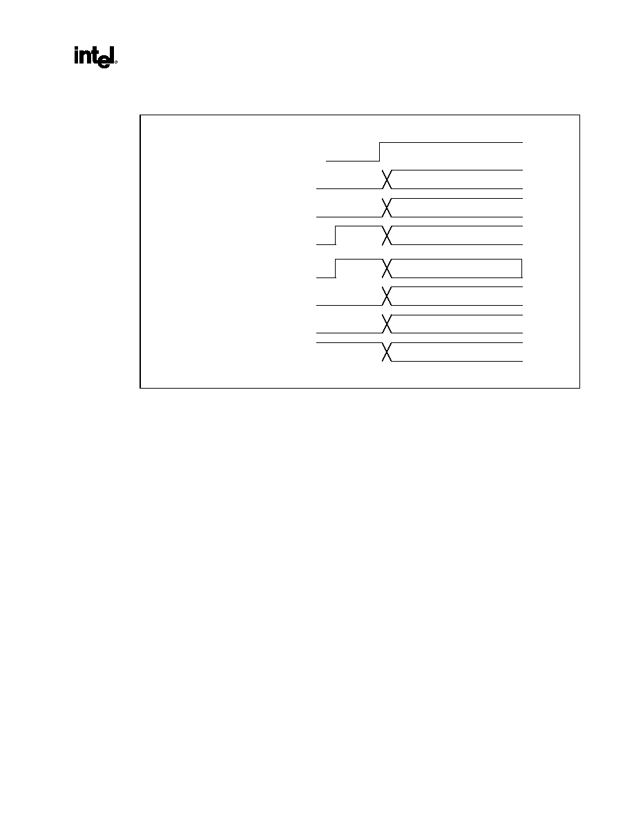
Intel
Æ
830 Chipset Family
298338-003 Datasheet
189
R
Figure 16. XOR Chain Test Mode Entry Events Diagram
PCIRST#
DVOA_D[3]
Don't care
DVOA_D[4]
Don't care
Don't care
Don't care
Don't care
Don't care
DVOA_D[6]
DVOA_D[7]
DVOA_D[8]
DVOA_D[11]
G_PAR
Don't care
The assertion of DVOA_D[6] high in Figure 16 is optional. The 830 Chipset family supports dual ended
termination for the CPU but only single ended termination is necessary when using the XOR test chains.
5.9.1.2 RAC
Chain
Initialization
On the RAC chain, special timing requirements need to be followed in order to use it. The event
sequence (see Section 5.9.1.2) to enter test mode for the RAC chain is identical to that for all other
chains and is shown in Figure 16 above. The application of test patterns to the inputs of the RAC chain
must adhere to the timing requirements shown in Figure 17. Table 45 lists the minimum and maximum
timings for the time parameters in Figure 17. This includes the maximum test enable (t1) and output
propagation delays (t2), and minimum period for the application of a test pattern (t3).
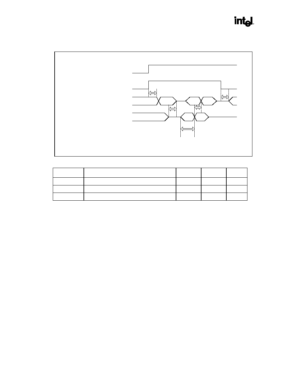
Intel
Æ
830 Chipset Family
190 Datasheet
298338-003
R
Figure 17. RAC Chain Timing Diagram
IOCTEn (internal signal)
NC (ball F12)
DQA
DQB
RQ
CTM(CFM)
CTMB(CFMB)
D0
D1
D1
D0
X
t1
t2
t3
t1
t2
PCIRST#
Table 45. RAC Chain Timing Descriptions
Symbol Description Min
Max
Unit
t1
IOCT test enable delay
0
100
ns
t2
I/O to IOCT Output delay
0
25
ns
t3
I/O connectivity sequence period
30
ns
Intel
Æ
830 Chipset Family
298338-003 Datasheet
191
R
5.9.1.3
XOR Chain Test Pattern Consideration for Differential Pairs
Below are the differential signals in the XOR chains that must be treated as pairs. Pin1 and Pin2 as
shown below must always be complementary to each other. For example, if a 1 is driven on ADSTB0, a
0 must be driven on ADSTB0# and vice versa. This will need to be considered when applying test
patterns to these chains.
Table 46. XOR Chain Differential Pairs
Pin1 Pin2
XOR
Chain
ADSTB0 ADSTB0# AGP1
ADSTB1 ADSTB1# AGP1
SBSTB SBSTB# AGP2
DVOADATA(0) DVOADATA(1)
DVO
PSTRB PSTRB# Hublink

Intel
Æ
830 Chipset Family
192 Datasheet
298338-003
R
5.9.1.4
XOR Chain Exclusion List
Please see below for a list of pins that are not included in the XOR chains (excluding all VCC/VSS):
1. GTL_REF0
2. GTL_REF1
3. CPURST#
4. GTL_RCOMP
5. HTCLK#
6. HTCLK
7. DREFCLK
8. DVOA_RCOMP
9. BLUE#
10. BLUE
11. GREEN
12. GREEN#
13. RED
14. RED#
15. GBIN
16. GBOUT
17. RESET#
18. AGP_RCOMP
19. AGPREF
20. HLREF
21. HL_RCOMP
22. SM_REF0
23. SM_REF1
Intel
Æ
830 Chipset Family
298338-003 Datasheet
193
R
5.9.1.5 NC
Balls
The 830 Chipset family contains four NC (No Connect) balls that are not used in any chipset features.
However, these four NC balls are used as input and/or output to some of the XOR test chains. The
following table lists the balls and associated XOR chain.
Table 47. NC Ball and Associated XOR Chain
Ball
XOR
Chain
1 E11
PSB2
2 E20
SM1
3 F20
SM1
4 F12
RAC

Intel
Æ
830 Chipset Family
194 Datasheet
298338-003
R
5.9.1.6
XOR Chain Connectivity/Ordering
The following tables contain the ordering for all of the 830 Chipset family XOR chains and pin to ball
mapping information:
Table 48. XOR Chain AGP1
Ball
Pin
XOR OUT
A19
SMA5
1 W25
GAD29
2 Y29
GAD31
3 V25
GAD27
4 W26
GAD28
5 W27
GAD30
6 W29
GAD26
7 V27
GAD22
8 V28
GAD23
9 V29
GAD25
10 U26
GAD24
11 U27
GAD21
12 U29
GDSTB1
13 U28 GDSTBB1
14 T25
GCBE3
15 T26
GAD20
16 T27 DVOC_D0
17 T29
GAD18
18 R24
GAD17
19 R25
GAD16
20 P29
GCBE1
21 N29
GAD12
22 N27
GAD15
23 N26
GAD14
24 M29
GAD8
25 M28
GAD9
26 M27
GAD11
27 M25
GAD13
28 L29
GDSTB0
29 L28 GDSTBB0
30 L27
GCBE0
31 L26
GAD4

Intel
Æ
830 Chipset Family
298338-003 Datasheet
195
R
32 K29
GAD6
33 K27
GAD7
34 K26 DVOB_D1
35 L24
GAD10
36 J29
GAD0
37 K25
GAD3
38 J28
GAD1
39 J27
GAD5
Table 49. XOR Chain AGP2
Ball
Pin
XOR OUT
A17
SMA9
1 AD29
GGNTB
2 AB25
GRBFB
3 AC27
GREQB
4 AC28
GST0
5 AC29
GST1
6 AA25
GSBA2
7 AB26
GPIPEB
8 AB27
GST2
9 AB29
GWBFB
10 Y24
GSBA3
11 AA27
GSBSTB
12 AA28 GSBSTBB
13 W24
GSBA6
14 AA24
GSBA1
15 Y26
GSBA5
16 AA29
GSBA0
17 Y27
GSBA4
18 Y28
GSBA7
19 R29 GFRAMEB
20 R27
GCBE2
21 R28 GDEVSELB
22 P28
GPAR
23 P27
GTRDYB
24 P26
GIRDYB
25 N25
GSTOPB

Intel
Æ
830 Chipset Family
196 Datasheet
298338-003
R
Table 50. XOR Chain DVO
Ball
Pin
XOR OUT
C16
SMBA1
1 AD20 DVO
CLKIN
2 AE21 DVO
INTR
3 AJ22
DVOD0
4 AH22
DVOD1
5 AG22
DVOD2
6 AF22 DVO
HSYNC
7 AJ23
DVOD3
8 AE22 DVO
FIELD
9 AH23
DVOD4
10 AG23
DVOD5
11 AF23 DVO
VSYNC
12 AD21 DVO
BLANK
13 AJ24 DVO
CLK
14 AG24 DVO
CLKB
15 AE23
DVOD6
16 AJ25
DVOD8
17 AE24
DVOD7
18 AH25
DVOD9
19 AG25
DVOD10
20 AJ26
DVOD11

Intel
Æ
830 Chipset Family
298338-003 Datasheet
197
R
Table 51. XOR Chain PSB1
Ball
Pin
XOR OUT
E17
SMCS0
1 G6 H_RS2B
2 D3
H_HITB
3 C1 H_ADSB
4 H6 H_RS0B
5 G5 H_DBSYB
6 F4 H_DRDYB
7 E3
H_A4
8 G4 H_TRDYB
9 J6 H_LOCKB
10 D1 H_HITMB
11 H4
H_RS1B
12 G3
H_A5
13 K6 H_REQ0B
14 E1
H_BNRB
15 K5 H_REQ2B
16 F2
H_A9
17 F1
H_A8
18 L6 H_REQ4B
19 K4 H_REQ3B
20 H2
H_A3
21 M6
H_A7
22 L4
H_BPRIB
23 M4 H_REQ1B
24 N4
H_A6
25 Y2
H_D32
26 AA1
H_D34
27 AA2
H_D38
28 AA4
H_D33
29 AB1
H_D36
30 AB3
H_D39
31 AC1
H_D45
32 AC2
H_D42
33 AC3
H_D49
34 AC4
H_D37
35 AA6
H_D35

Intel
Æ
830 Chipset Family
198 Datasheet
298338-003
R
36 AD1
H_D41
37 AD2
H_D40
38 AD4
H_D47
39 AE1
H_D59
40 AE3
H_D52
41 AF1
H_D63
42 AF2
H_D55
43 AC6
H_D44
44 AE4
H_D57
45 AB6
H_D43
46 AF3
H_D46
47 AG1
H_D58
48 AG2
H_D53
49 AE5
H_D51
50 AD6
H_D48
51 AF4
H_D54
52 AG3
H_D62
53 AH3
H_D50
54 AG4
H_D60
55 AH4
H_D61
56 AJ3
H_D56

Intel
Æ
830 Chipset Family
298338-003 Datasheet
199
R
Table 52. XOR Chain PSB2
Ball
Pin
XOR OUT
E11
NC
1 F3
H_A11
2 J4 H_DEFERB
3 H3
H_A28
4 G1
H_A13
5 J3
H_A10
6 H1
H_A15
7 K3
H_A31
8 L3
H_A23
9 J2
H_A19
10 J1
H_A25
11 N5
H_A14
12 M3
H_A29
13 K1
H_A22
14 L2
H_A20
15 L1
H_A24
16 M2
H_A18
17 P6
H_A12
18 N3
H_D6
19 M1
H_A30
20 P4
H_A16
21 P3
H_D9
22 N1
H_A26
23 P2
H_D15
24 P1
H_D1
25 R4
H_A21
26 R3
H_D10
27 R2
H_D17
28 R1
H_D5
29 T5
H_A27
30 T4
H_A17
31 T3
H_D14
32 T1
H_D18
33 U4
H_D0
34 U6
H_D4
35 U3
H_D20

Intel
Æ
830 Chipset Family
200 Datasheet
298338-003
R
36 U2
H_D3
37 U1
H_D11
38 V4
H_D8
39 V3
H_D16
40 V2
H_D30
41 V1
H_D24
42 W4
H_D13
43 W3
H_D19
44 V6
H_D12
45 W1
H_D23
46 W5
H_D7
47 Y3
H_D31
48 Y4
H_D21
49 W6
H_D2
50 Y6
H_D26
51 Y1
H_D25
52 AA3
H_D22
53 AB4
H_D28
54 AD3
H_D27
55 AB5
H_D29
Intel
Æ
830 Chipset Family
298338-003 Datasheet
201
R
Table 53. XOR Chain GPIO
Ball
Pin
XOR OUT
C15
SMA11
1 AD28
HSYNC
2 AC24 AGP
BUSY
3 AD27 DDC1
DATA
4 AC25 I2C
DATA
5 AD26 DDC2
DATA
6 AE29
VSYNC
7 AE27 DDC1
CLK
8 AE26 DDC2
CLK
9 AD25 I2C
CLK
Table 54. XOR Chain HUB
Ball
Pin
XOR OUT
A18
SMA4
1 E28
HLD7
2 G25
HLRQM
3 E29
HLD6
4 F27
HLD5
5 G26
HLD0
6 F28 HLSTBB
7 G29
HLSTB
8 G27
HLRQI
9 F29
HLD4
10 H26
HLSTOP
11 H27
HLD3
12 H28
HLD1
13 H29
HLD2

Intel
Æ
830 Chipset Family
202 Datasheet
298338-003
R
Table 55. XOR Chain SM1
Ball
Pin
XOR OUT
A20
SMA0
1 C24 SMRCLK
2 A24 SMOCLK
3 G22
SMD42
4 A23
SMD44
5 D22
SMD43
6 F21
SMD45
7 D21
SMD46
8 E20
NC
9 F20
NC
10 A22
SMD47
12 B20
SMA1
14 D19
SMCAS
15 F18
SMDQM0
16 B19
SMA2
17 C17
SMA6
18 B17
SMA8
20 D15
SMCS3
22 F13
SMDQM7
23 A15
SMCLK0
24 B14
SMCLK2
26 D13 SMDQM2
27 C13
SMCKE2
28 A13
SMCKE0
32 D12 SMDQM3
33 A11
SMD49
34 B11
SMD50
35 B10
SMD52
36 F11
SMD48
37 A9
SMCKE3
38 C9
SMCKE1
39 D9
SMD54
40 F10
SMD51
42 B8
SMD53
43 F9
SMD56
44 B7
SMD55
Intel
Æ
830 Chipset Family
298338-003 Datasheet
203
R
45 D7
SMD59
46 A6
SMD57
47 C6
SMD58
48 E6
SMD61
49 B5
SMD60
50 A4
SMD62
51 A3
SMCLK3
53 B2
SMCLK1
54 D4
SMD63
Table 56. XOR Chain SM2
Ball
Pin
XOR OUT
C19
SMA3
1 D29
SMD0
2 C29
SMD1
3 C28
SMD33
4 B28
SMD34
5 E27
SMD32
6 D27
SMD2
7 E26
SMD35
8 C27
SMD3
9 A27
SMD4
10 C26
SMD36
11 B26
SMD5
12 E24
SMD6
13 A26
SMD38
14 D25
SMD37
15 C25
SMD7
16 B25
SMD9
17 E23
SMD8
18 D24
SMD39
19 A25
SMD41
20 F23
SMD40
21 C23
SMD10
22 B23
SMD12
23 F22
SMD11
24 C22
SMD13

Intel
Æ
830 Chipset Family
204 Datasheet
298338-003
R
25 E21
SMD14
26 B22
SMD15
27 A21
SMWE
28 C20
SMRAS
29 E18 SMDQM4
30 D18 SMDQM1
31 F17
SMDQM5
32 C18
SMA7
33 D16
SMCS2
34 B16
SMBA0
35 A16
SMA10
36 C14
SMA12
37 F14
SMDQM6
38 C12
SMD16
39 C11
SMD18
40 A10
SMD19
41 C10
SMD20
42 D10
SMD17
43 F8
SMD27
44 E9
SMD23
45 C8
SMD21
46 A7
SMD22
47 C7
SMD24
48 E8
SMD25
49 D6
SMD29
50 A5
SMD26
51 C5
SMD28
52 B4
SMD30
53 C4
SMD31

Intel
Æ
830 Chipset Family
298338-003 Datasheet
205
R
Table 57. XOR Chain CMOS
Ball
Pin
XOR OUT
F16
SMCS1
1 AG6
GCLK
2 AJ6
RCLK
3 AF7
SCK
4 AH7
CMD
5 AJ7
SIO
Table 58. XOR Chain RAC
Ball
Pin
XOR OUT
F12
NC
1 AJ20
DQA7
2 AG20
DQA6
3 AJ19
DQA5
4 AG19
DQA4
5 AJ18
DQA3
6 AG18
DQA2
7 AJ17
DQA1
8 AG17
DQA0
9 AH15
CTM
10 AJ16
CFM
11 AJ15
CTM_B
12 AH16
CFM_B
13 AJ14
RQ7
14 AG14
RQ6
15 AJ13
RQ5
16 AG13
RQ4
17 AH13
RQ3
18 AG12
RQ2
19 AJ12
RQ1
20 AG11
RQ0
21 AJ11
DQB0
22 AH10
DQB1
23 AJ10
DQB2
24 AG10
DQB3
25 AJ9
DQB4

Intel
Æ
830 Chipset Family
206 Datasheet
298338-003
R
26 AG9
DQB5
27 AJ8
DQB6
28 AG8
DQB7

Intel
Æ
830 Chipset Family
298338-003 Datasheet
207
R
6
Intel 830 Chipset Family
Performance
The system performance for the Intel 830 Chipset family GMCH-M described below is a breakdown of
the data streams that complement the Mobile Intel Pentium
III
Processor-M. This section describes the
overall performance of the GMCH-M. Following categories of performance are examined:
∑
CPU/830 Chipset family GMCH-M: Intel 830 Chipset family supports Mobile Intel Pentium
III
Processor-M
∑
System Memory: Intel 830 Chipset GMCH-M supports PC133 main memory
∑
AGP only available with 830M and 830MP Chipset
∑
DVO only available with 830M and 830MG Chipset
Table 59. System Bandwidths
Interface Clock
Speed
(MHz)
Samples Per
Clock
Data Rate
(Mega-samples/s)
Data Width
(Bytes)
Bandwidth
(MB/s)
CPU Bus
133
1
133
8
1066
SDRAM 133
1
133
8 1064
AGP 2.0
66
4
266
4
1066
DVO 165 2
330
1.5 495
DVO
Gang mode
165 2
330 3
990
PCI 2.2
33
1
33
4
133
NOTE: *Theoretical Bandwidths only.

Intel
Æ
830 Chipset Family
208 Datasheet
298338-003
R
7 Mechanical
Specification
7.1
Intel 830MP Chipset GMCH-M Ballout Diagram
Figure 18 and Figure 19 show the ballout of the Intel 830MP Chipset.
Intel
Æ
830 Chipset Family
298338-003 Datasheet
209
R
Figure 18. Intel 830MP Ballout Diagram (Left)
1
2
3
4
5
6
7
8
9
10
11
12
13
14
A
SM_CLK3
SMD62
SMD26
SMD57
SMD22
VCC_SM
SM_CKE3
SMD19
SMD49
VCC_SM
SM_CK
E0
VSS
B
SM_CLK1
VSS
SMD30
SMD60
VSS
SMD55
SMD53
VSS
SMD52
SMD50
VSS
VSS
SM_CLK2
C
H_ADS#
GTL_
RCOMP
VSS
SMD31
SMD28
SMD58
SMD24
SMD21
SM_CK
E1
SM
D20
SMD18
SMD16
SM_CKE2
SMA12
D
H_HITM#
VSS
H_HIT#
SMD63
VCC_SM
SMD29
SMD59
VCC_SM
SMD54
SMD17
VCC_SM
SM_DQM3
SM_DQM2
VCC_SM
E
H_BNR#
VTT
H_A4#
VSS
SM_VREF
1
SMD61
VSS
SMD25
SMD23
VSS
NC
VCC_SM
VSS
VSS
F
H_A8#
H_A9#
H_A11#
H_DRDY#
VTT
SM_RCOMP
VCCQ _SM
SMD27
SMD56
SMD51
SMD48
NC
SM_DQM7
SM_DQM6
G
H_A13#
VSS
H_A5#
H_TRDY#
H_DBSY#
H_RS2#
VCCA_
CPLL
VSSA_CPLL
VSS
VCC_SM
VCC_SM
H
H_A15#
H_A3#
H_A28#
H_RS1#
VSS
H_RS0#
VCC
J
H_A25#
H_A19#
H_A10#
H_DEFER#
VTT
H_LOCK#
GTL_REFA
K
H_A22#
V
SS
H_A31#
H_REQ3#
H_REQ2#
H_REQ0#
VCC
L
H_A24#
H_A20#
H_A23#
H_BPRI#
VSS
H_REQ4#
VCC
M
H_A30#
H_A18#
H_A29#
H_REQ1#
VTT
H_A7#
VSS
VSS
VCC
N
H_A26#
VSS
H_D6#
H_A6#
H_A14#
VCC
VSS
VSS
VSS
P
H_D1#
H_D15#
H_D9#
H_A16#
VSS
H_A12#
VCC
VSS
VSS
R
H_D5#
H_D17#
H_D10#
H_A21#
VTT
CPU_RST#
VCC
VSS
VSS
T
H_D18#
VSS
H_D14#
H_A17#
H_A27#
VCC
VCC
VSS
VSS
U
H_D11#
H_D3#
H_D20#
H_D0#
VSS
H_D4#
VSS
VSS
VSS
V
H_D24#
H_D30#
H_D16#
H_D8#
VTT
H_D12#
VSS
VSS
VDD_LM
W
H_D23#
VSS
H_D19#
H_D13#
H_D7#
H_D2#
VCC
Y
H_D25#
H_D32#
H_D31#
H_D21#
VSS
H_D26#
VCC
AA
H_D34#
H_D38#
H_D22#
H_D33#
VTT
H_D35#
GTL_REFB
AB
H_D36#
VSS
H_D39#
H_D28#
H_D29#
H_D43#
VCC
AC
H_D45#
H_D42#
H_D49#
H_D37#
VSS
H_D44#
VSS
VCC_CMOS
VCC_CMOS
VCC_LM
V
CC_LM
AD
H_D41#
H_D40#
H_D27#
H_D47#
VTT
H_D48#
VSSA_HPLL
VSS
VSS
VSS
VCC_LM
VCC_LM
VCC_LM
RAMREF
[0]
AE
H_D59#
VSS
H_D52#
H_D57#
H_D51#
VCCA_
HPLL
VCC_CMOS
VSS
VSS
VSS
VSS
VSS
VSS
RAMREF
[1]
AF
H_D63#
H_D55#
H_D46#
H_D54#
VSS
VCC_CM OS
SCK
VSS
VSS
VSS
VSS
VSS
VSS
VSS
AG
H_D58#
H_D53#
H_D62#
H_D60#
VTT
GCLK
VSS
DQB7
DQB5 DQB3
RQ0
RQ2
RQ4
RQ6
AH
VSS
H_D50#
H_D61#
HTCLK#
VSS
CMD VSS
VSS
DQB1
VSS
VSS
RQ3
VSS
AJ
H_D56#
HTCLK
VSS
GM_RCLK
SIO
DQB6
DQB4 DQB2
DQB0
RQ1 RQ5 RQ7
1
2
3
4
5
6
7
8
9
10
11
12
13
14
RESERVED
RESERVED
RESERVED
RESERVED
RESERVED
RESERVED
RESERVED
RESERVED
RESERVED
RESERVED
RESERVED
RESERVED
RESERVED
RESERVED
RESERVED
RESERVED
RESERVED
RESERVED
RESERVED
RESERVED
RESERVED
RESERVED
RESERVED

Intel
Æ
830 Chipset Family
210 Datasheet
298338-003
R
Figure 19. Intel 830MP Ballout (Right)
15
16
17
18
19
20
21
22
23
24
25
26
27
28
29
SM_
CLK0
SMA10
SMA9
SMA4
SMA5
SMA0
SMWE
SMD47
SMD44
SM_OCLK
SMD41
SMD38
SMD4
A
VSS
SMBA0
SMA8
VSS
SMA2
SMA1
VSS
SMD15
SMD12
VSS
SMD9
SMD5
VSS
SMD34
B
SMA11
SMBA1
SMA6
SMA7
SMA3
SMRAS
VSS
SMD13
SMD10
SM_R CLK
SMD7
SMD36
SMD3
SMD33
SMD1
C
SM_CS3#
SM_CS2#
VCC_SM
SMDQM1
SMCAS
VCC_SM
SMD46
SMD43
VCC_SM
SMD39
SMD37
VCC_SM
SMD2
VSS
SMD0
D
VCCQ_
SM
VSS
SM_CS0#
SMDQM4
VSS
NC
SMD14
VSS
SMD8
SMD6
VSS
SMD35
SMD32
HL7
HL6
E
VCCQ_
SM
SM_CS1#
SMDQM5
SMDQM0
VSS
NC
SMD4
5
SMD11
SMD40
SM_VREF0
VCCA_
PLL1
VCC_ HUB
HL5
HLSTRB#
HL4
F
VCCQ_SM
VCCQ_SM
VSS
SMD42
VCC_SM
VSSA_
DPLL1
HL8
HL0
HL9
VSS
HLSTRB
G
VCC
HLREF
VSS
HL10
HL3
HL1
HL2
H
HRCOMP
VCC_HUB
AGPREF
VCC_ AGP
G_AD5
G_AD1
G_AD0
J
VCC
AGP_
RCOMP
G_AD3
G_AD2
G_AD7
VSS
G_AD6
K
VCC_AGP
G_AD10
VSS
G_AD4
G_CBE0#
AD_STB0#
AD_ST
B0
L
VCC
VCC
VSS
VSS
VCC
G_AD13
VCC_ AGP
G_AD11
G_AD9
G_AD8
M
VSS
VSS
VSS
VSS
VCCQ_AGP
G_STOP#
G_AD14
G_AD15
VSS
G_AD12
N
VSS
VSS
VSS
VCC
VCC
VSS
G_IRDY#
G_TRDY#
G_PAR
G_CBE1#
P
VSS
VSS
VSS
VCC
G_AD17
G_AD16
VCC_ AGP
G_CBE2#
G_DEVSEL#
G_FRAME#
R
VSS
VSS
VSS
VCC
VCC
G_CBE3#
G_AD20
G_AD19
VSS
G_AD18
T
VSS
VSS
VSS
VSS
VCC_AGP
VSS
G_AD24
G_AD21
AD_STB1#
AD_STB1
U
VDD_LM
VDD_LM
VSS
VSS
VCC
G_AD27
VCC_ AGP
G_AD22
G_AD23
G_AD25
V
VDDQ_A
GP
SBA6
G_AD29
G_AD28
G_AD30
VSS
G_AD26
W
VCC
SBA3
VSS
SBA5
SBA4
SBA7
G_AD31
Y
VCC_AGP
SBA1
SBA2
VCC_ AGP
SB_STB
SB_STB#
SBA0
AA
VSS
RESET#
RBF#
PIPE#
ST2
VSS
WBF#
AB
DREFCLK
VCCA_
DPLL0
VCC_DVO
DVOA_
RCOMP
VSS
AGPB
USY#
I2C_
DATA
VSS
REQ#
ST0
ST1
AC
VDD_LM
VDD_LM
VCC_LM
VCC_LM
VCC_LM
DVOA_CLK
INT
DVOA_
BLANK#
VSS
VCC_GPIO
GBOUT
I2C_CLK
DDC2_DA
DDC1_DA
HSYNC
G_GNT#
AD
VDD_LM
VDD_LM
VSS
VCC_LM
VSS
VSSA_DPLL
0
DVOA_
INTR#
DVOA_FLD
/ST
L
DVOA_D6
DVOA_D7
VCC_
GPIO
DDC2_CK
DDC1_CK
VSS
VSYNC
AE
VSS
VSS
VSS
VSS
VSS
VSS
VCC_DVO
DVOA_HSYNC
DVOA_VSYNC
VCC_DVO
VSS
VCCA_
DAC
VSS
RED#
RED
AF
VSS
VSS
DQA0 DQA2 DQA4
DQA6
VSS
DVOA_D2
DVOA_D5
DVOA_CLK
#
DVO_D10
G
BIN
VCCA_
DAC
GREEN#
GREEN
AG
CTM
CFM#
VSS
VSS
VSS
VSS
VSS
DVOA_D1
DVOA_D4
VSS
DVO_D9
VSSA_DAC
BLUE#
BLUE
AH
CTM# CFM DQA1 DQA3 DQA5
DQA7
VSS
DVOA_D0
DVOA_D3
DVOA_CLK
DVO_D11
REFSET
AJ
RESERVED
RESERVED
RESERVE
D
RESERVED
RESERVED
RESERVED
RESERVED
RESERVED
RESERVED
RESERVED
RESERVED
RESERVED
RESERVED
RESERVED
RESERVED
RESERVED
RESERVED
RESERVED
RESERVED
RESERVED
RESERVED
RESERVED
RESERVED
RESERVED
RESERVED
RESERVED
RESERVED
RESERVED
RESERVED
RESERVED
RESERVED
RESERVED
RESERVED
RESERVED
RESERVED
RESERVED
RESERVED
RESERVED
RESERVED
RESERVED
RESERVED
RESERVED
RESERVED
RESERVED
DVOA_D8
RESERVED
RESERVED
RESERVED
RESERVED
RESERVED
RESERVED
RESERVED

Intel
Æ
830 Chipset Family
298338-003 Datasheet
211
R
7.2
Intel 830M Chipset GMCH-M Ballout Diagram
Figure 20 and Figure 21 show the ballout of the Intel 830M Chipset.

Intel
Æ
830 Chipset Family
212 Datasheet
298338-003
R
Figure 20. Intel 830M Chipset Ballout Diagram (Left)
1
2
3
4
5
6
7
8
9
10
11
12
13
14
A
SM_CLK3
SMD62
SMD26
SMD57
SMD22
VCC_SM
SM_CKE3
SMD19
SMD49
VCC_SM
SM_CK
E0
VSS
B
SM_CLK1
VSS
SMD30
SMD60
VSS
SMD55
SMD53
VSS
SMD52
SMD50
VSS
VSS
SM_CLK2
C
H_ADS#
GTL_
RCOMP
VSS
SMD31
SMD28
SMD58
SMD24
SMD21
SM_CK
E1
SMD20
SMD18
SMD16
SM_CKE2
SMA12
D
H_HITM#
VSS
H_HIT#
SMD63
VCC_SM
SMD29
SMD59
VCC_SM
SMD54
SMD17
VCC_SM
SM_DQM3
SM_DQM2
VCC_SM
E
H_BNR#
VTT
H_A4#
VSS
SM_VREF
1
SMD61
VSS
SMD25
SMD23
VSS
NC
VCC_SM
VSS
VSS
F
H_A8#
H_A9#
H_A11#
H_DRDY#
VTT
SM_RCOMP
VCCQ _SM
SMD27
SMD56
SMD51
SMD48
NC
SM_DQM7
SM_DQM6
G
H_A13#
VSS
H_A5#
H_TRDY#
H_DBSY#
H_RS2#
VCCA_
CPLL
VSSA_CPLL
VSS
VCC_SM
VCC_SM
H
H_A15#
H_A3#
H_A28#
H_RS1#
VSS
H_RS0#
VCC
J
H_A25#
H_A19#
H_A10#
H_DEFER#
VTT
H_LOCK#
GTL_REFA
K
H_A22#
V
SS
H_A31#
H_REQ3#
H_REQ2#
H_REQ0#
VCC
L
H_A24#
H_A20#
H_A23#
H_BPRI#
VSS
H_REQ4#
VCC
M
H_A30#
H_A18#
H_A29#
H_REQ1#
VTT
H_A7#
VSS
VSS
VCC
N
H_A26#
VSS
H_D6#
H_A6#
H_A14#
VCC
VSS
VSS
VSS
P
H_D1#
H_D15#
H_D9#
H_A16#
VSS
H_A12#
VCC
VSS
VSS
R
H_D5#
H_D17#
H_D10#
H_A21#
VTT
CPU_RST#
VCC
VSS
VSS
T
H_D18#
VSS
H_D14#
H_A17#
H_A27#
VCC
VCC
VSS
VSS
U
H_D11#
H_D3#
H_D20#
H_D0#
VSS
H_D4#
VSS
VSS
VSS
V
H_D24#
H_D30#
H_D16#
H_D8#
VTT
H_D12#
VSS
VSS
VDD_LM
W
H_D23#
VSS
H_D19#
H_D13#
H_D7#
H_D2#
VCC
Y
H_D25#
H_D32#
H_D31#
H_D21#
VSS
H_D26#
VCC
AA
H_D34#
H_D38#
H_D22#
H_D33#
VTT
H_D35#
GTL_REFB
AB
H_D36#
VSS
H_D39#
H_D28#
H_D29#
H_D43#
VCC
AC
H_D45#
H_D42#
H_D49#
H_D37#
VSS
H_D44#
VSS
V
CC_CMOS
VCC_CMOS
VCC_LM
V
CC_LM
AD
H_D41#
H_D40#
H_D27#
H_D47#
VTT
H_D48#
VSSA_HPLL
VSS
VSS
VSS
VCC_LM
VCC_LM
VCC_LM
RAMREF
[0]
AE
H_D59#
VSS
H_D52#
H_D57#
H_D51#
VCCA_
HPLL
VCC_CMOS
VSS
VSS
VSS
VSS
VSS
VSS
RAMREF
[1]
AF
H_D63#
H_D55#
H_D46#
H_D54#
VSS
VCC_CM OS
SCK
VSS
VSS
VSS
VSS
VSS
VSS
VSS
AG
H_D58#
H_D53#
H_D62#
H_D60#
VTT
GCLK
VSS
DQB7
DQB5
DQB3
RQ0 RQ2
RQ4
RQ6
AH
VSS
H_D50#
H_D61#
HTCLK#
VSS
CMD
VSS
VSS
DQB1
VSS
VSS
RQ3
VSS
AJ
H_D56#
HTCLK
VSS
GM_RCLK
SIO
DQB6
DQB4
DQB2
DQB0
RQ1
RQ5
RQ7
1
2
3
4
5
6
7
8
9
10
11
12
13
14
RESERVED
RESERVED
RESERVED
RESERVED
RESERVED
RESERVED
RESERVED
RESERVED
RESERVED
RESERVED
RESERVED
RESERVED
RESERVED
RESERVED
RESERVED
RESERVED
RESERVED
RESERVED
RESERVED
RESERVED
RESERVED
RESERVED
RESERVED
Intel
Æ
830 Chipset Family
298338-003 Datasheet
213
R
Figure 21. Intel 830M Chipset Ballout Diagram (Right)
15
16
17
18
19
20
21
22
23
24
25
26
27
28
29
SM_
CLK0
SMA10
SMA9
SMA4
SMA5
SMA0
SMWE
SMD47
SMD44
SM_OCLK
SMD41
SMD38
SMD4
A
VSS
SMBA0
SMA8
VSS
SMA2
SMA1
VSS
SMD15
SMD12
VSS
SMD9
SMD5
VSS
SMD34
B
SMA11
SMBA1
SMA6
SMA7
SMA3
SMRAS
VSS
SMD13
SMD10
SM_R
CLK
SMD7
SMD36
SMD3
SMD33
SMD1
C
SM_CS3#
SM_CS2#
VCC_SM
SMDQM1
SMCAS
VCC_SM
SMD46
SMD43
VCC_SM
SMD39
SMD37
VCC_SM
SMD2
VSS
SMD0
D
VCCQ_
SM
VSS
SM_CS0#
SMDQM4
VSS
NC
SMD14
VSS
SMD8
SMD6
VSS
SMD35
SMD32
HL7
HL6
E
VCCQ_
SM
SM_CS1#
SMDQM5
SMDQM0
VSS
NC
SMD4
5
SMD11
SMD40
SM_VREF0
VCCA_
PLL1
VCC_ HUB
HL5
HLSTRB#
HL4
F
VCCQ_SM
VCCQ_SM
VSS
SMD42
VCC_SM
VSSA_
DPLL1
HL8
HL0
HL9
VSS
HLSTRB
G
VCC
HLREF
VSS
HL10
HL3
HL1
HL2
H
HRCOMP
VCC_HUB
AGPREF/
DVOBC_REF
VCC_ AGP
G_AD5/
G_AD1/
G_AD0/
J
VCC
AGP_
RCOMP
G_AD3/
G_AD2/
G_AD7/
VSS
G_AD6/
K
VCC_AGP
G_AD10/
VSS
G_AD4/
G_CBE0#/
AD_STB0#/
AD_STB0/
L
VCC
VCC
VSS
VSS
VCC
G_AD13/
VCC_ AGP
G_AD11/
G_AD9/
G_AD8/
M
VSS
VSS
VSS
VSS
VCCQ_AGP
G_STOP#
G_AD14/
G_AD15
VSS
G_AD12/
N
VSS
VSS
VSS
VCC
VCC
VSS
G_IRDY#/
G_TRDY#/
G_PAR
G_CBE1#/
P
VSS
VSS
VSS
VCC
G_AD17/
G_AD16/
VCC_ AGP
G_CBE2#
G_DEVSEL#/
G_FRAME#/
R
VSS
VSS
VSS
VCC
VCC
G_CBE3#/
G_AD20/
G_AD19/
VSS
G_AD18/
T
VSS
VSS
VSS
VSS
VCC_AGP
VSS
G_AD24/
G_AD21/
AD_STB1#/
AD_STB1/
U
VDD_LM
VDD_LM
VSS
VSS
VCC
G_AD27/
VCC_ AGP
G_AD22/
G_AD23/
G_AD25/
V
VDDQ_AGP
SBA6
G_AD29/
G_AD28/
G_AD30/
VSS
G_AD26/
W
VCC
SBA3
VSS
SBA5
SBA4
SBA7
G_AD31/
Y
VCC_AGP
SBA1
SBA2
VCC_ AGP
SB_STB
SB_STB#
SBA0
AA
VSS
RESET#
RBF#
PIPE#
ST2
VSS
WBF#
AB
DREFCLK
VCCA_
DPLL0
VCC_DVO
DVOA_
RCOMP
VSS
AGPBUSY#
I2C_
DATA
VSS
REQ#
ST0
ST1
AC
VDD_LM
VDD_LM
VCC_LM
VCC_LM
VCC_LM
DVOA_CLK
INT
DVOA_
BLANK#
VSS
VCC_GPIO
GBOUT
I2C_CLK
DDC2_DA
DDC1_DA
HSYNC
G_GNT#
AD
VDD_LM
VDD_LM
VSS
VCC_LM
VSS
VSSA_DPLL
0
DVOA_
INTR#
DVOA_FLD
/STL
DVOA_D6
DVOA_D7 VCC_
GPIO
DDC2_CK
DDC1_CK
VSS
VSYNC
AE
VSS
VSS
VSS
VSS
VSS
VSS
VCC_DVO
DVOA_HSYNC
DVOA_VSYNC
VCC_DVO
VSS
VCCA_
DAC
VSS
RED#
RED
AF
VSS
VSS
DQA0
DQA2
DQA4
DQA6
VSS
DVOA_D2
DVOA_D5
DVOA_CLK
#
DVOA_D10
GBIN
VCCA_
DAC
GREEN#
GREEN
AG
CTM
CFM#
VSS
VSS
VSS
VSS
VSS
DVOA_D1
DVOA_D4
VSS
DVOA_D9
VSSA_DAC
BLUE#
BLUE
AH
CTM#
CFM
DQA1
DQA3
DQA5
DQA7
VSS
DVOA_D0
DVOA_D3
DVOA_CLK
DVOA_D8
DVOA_D11
REFSET
AJ
RESERVED
RESERVED
RESERVED
RESERVED
RESERVED
RESERVED
RESERVED
RESERVED
RESERVED
RESERVED
RESERVED
RESERVED
RESERVED
DVOB_D2
DVOB_VSYNC
DVOB_HSYNC
DVOB_D0
DVOB_D1
DVOB_D4
DVOB_D5
DVOB_D8
DVOB_D3
DVOB_D7
DVOB_CLK#
DVOB_CLK
DVOB_D6
DVOB_D9
DVOB_D11
DVOBC_C
LKINT#
DVOB_FL
D/STL
DVOB_D10
DVOB_BL
ANK#
M_DDC1_
CLK
M_I2C_C
LK
M_DDC1_
DATA
M_I2C_
DATA
DVOC_
VSYNC
DVOC_
HSYNC
DVOC_BL
ANK#
DVOC_D0
DVOC_D1
DVOC_D5
DVOC_D7
DVOC_D2
DVOC_CLK#
DVOC_CLK
DVOC_D6
DVOC_D4
DVOC_D3
DVOC_D8
DVOC_D10
DVOC_D11
DVOBC_INTR#/
DPMS_CLK
DVOC_D9
DVOC_FLD/
STL

Intel
Æ
830 Chipset Family
214 Datasheet
298338-003
R
7.3
Intel 830MG GMCH-M Ballout Diagram
Figure 22 and Figure 23 show the ballout of the Intel 830MG Chipset.
Intel
Æ
830 Chipset Family
298338-003 Datasheet
215
R
Figure 22. Intel 830MG Chipset Ballout Diagram (Left)
1
2
3
4
5
6
7
8
9
10
11
12
13
14
A
SM_CLK3
SMD62
SMD26
SMD57
SMD22
VCC_SM
SM_CKE3
SMD19
SMD49
VCC_SM
SM_CK
E0
VSS
B
SM_CLK1
VSS
SMD30
SMD60
VSS
SMD55
SMD53
VSS
SMD52
SMD50
VSS
VSS
SM_CLK2
C
H_ADS#
GTL_
RCOMP
VSS
SMD31
SMD28
SMD58
SMD24
SMD21
SM_CK
E1
SMD20
SMD18
SMD16
SM_CKE2
SMA12
D
H_HITM#
VSS
H_HIT#
SMD63
VCC_SM
SMD29
SMD59
VCC_SM
SMD54
SMD17
VCC_SM
SM_DQM3
SM_DQM2
VCC_SM
E
H_BNR#
VTT
H_A4#
VSS
SM_VREF
1
SMD61
VSS
SMD25
SMD23
VSS
NC
VCC_SM
VSS
VSS
F
H_A8#
H_A9#
H_A11#
H_DRDY#
VTT
SM_RCOMP
VCCQ _SM
SMD27
SMD56
SMD51
SMD48
NC
SM_DQM7
SM_DQM6
G
H_A13#
VSS
H_A5#
H_TRDY#
H_DBSY#
H_RS2#
VCCA_
CPLL
VSSA_CPLL
VSS
VCC_SM
VCC_SM
H
H_A15#
H_A3#
H_A28#
H_RS1#
VSS
H_RS0#
VCC
J
H_A25#
H_A19#
H_A10#
H_DEFER#
VTT
H_LOCK#
GTL_REFA
K
H_A22#
V
SS
H_A31#
H_REQ3#
H_REQ2#
H_REQ0#
VCC
L
H_A24#
H_A20#
H_A23#
H_BPRI#
VSS
H_REQ4#
VCC
M
H_A30#
H_A18#
H_A29#
H_REQ1#
VTT
H_A7#
VSS
VSS
VCC
N
H_A26#
VSS
H_D6#
H_A6#
H_A14#
VCC
VSS
VSS
VSS
P
H_D1#
H_D15#
H_D9#
H_A16#
VSS
H_A12#
VCC
VSS
VSS
R
H_D5#
H_D17#
H_D10#
H_A21#
VTT
CPU_RST#
VCC
VSS
VSS
T
H_D18#
VSS
H_D14#
H_A17#
H_A27#
VCC
VCC
VSS
VSS
U
H_D11#
H_D3#
H_D20#
H_D0#
VSS
H_D4#
VSS
VSS
VSS
V
H_D24#
H_D30#
H_D16#
H_D8#
VTT
H_D12#
VSS
VSS
VDD_LM
W
H_D23#
VSS
H_D19#
H_D13#
H_D7#
H_D2#
VCC
Y
H_D25#
H_D32#
H_D31#
H_D21#
VSS
H_D26#
VCC
AA
H_D34#
H_D38#
H_D22#
H_D33#
VTT
H_D35#
GTL_REFB
AB
H_D36#
VSS
H_D39#
H_D28#
H_D29#
H_D43#
VCC
AC
H_D45#
H_D42#
H_D49#
H_D37#
VSS
H_D44#
VSS
V
CC_CMOS
VCC_CMOS
VCC_LM
V
CC_LM
AD
H_D41#
H_D40#
H_D27#
H_D47#
VTT
H_D48#
VSSA_HPLL
VSS
VSS
VSS
VCC_LM
VCC_LM
VCC_LM
RAMREF
[0]
AE
H_D59#
VSS
H_D52#
H_D57#
H_D51#
VCCA_
HPLL
VCC_CMOS
VSS
VSS
VSS
VSS
VSS
VSS
RAMREF
[1]
AF
H_D63#
H_D55#
H_D46#
H_D54#
VSS
VCC_CM OS
SCK VSS
VSS
VSS
VSS
VSS
VSS
VSS
AG
H_D58#
H_D53#
H_D62#
H_D60#
VTT
GCLK
VSS
DQB7
DQB5
DQB3
RQ0
RQ2
RQ4
RQ6
AH
VSS
H_D50#
H_D61#
HTCLK#
VSS
CMD
VSS
VSS
DQB1
VSS
VSS
RQ3
VSS
AJ
H_D56#
HTCLK
VSS
GM_RCLK
SIO
DQB6
DQB4
DQB2
DQB0
RQ1
RQ5
RQ7
1
2
3
4
5
6
7
8
9
10
11
12
13
14
RESERVED
RESERVED
RESERVED
RESERVED
RESERVED
RESERVED
RESERVED
RESERVED
RESERVED
RESERVED
RESERVED
RESERVED
RESERVED
RESERVED
RESERVED
RESERVED
RESERVED
RESERVED
RESERVED
RESERVED
RESERVED
RESERVED
RESERVED

Intel
Æ
830 Chipset Family
216 Datasheet
298338-003
R
Figure 23. Intel 830MG Chipset Ballout Diagram (Right)
15
16
17
18
19
20
21
22
23
24
25
26
27
28
29
SM_
CLK0
SMA10
SMA9
SMA4
SMA5
SMA0
SMWE
SMD47
SMD44
SM_OCLK
SMD41
SMD38
SMD4
A
VSS
SMBA0
SMA8
VSS
SMA2
SMA1
VSS
SMD15
SMD12
VSS
SMD9
SMD5
VSS
SMD34
B
SMA11
SMBA1
SMA6
SMA7
SMA3
SMRAS
VSS
SMD13
SMD10
SM_R
CLK
SMD7
SMD36
SMD3
SMD33
SMD1
C
SM_CS3#
SM_CS2#
VCC_SM
SMDQM1
SMCAS
VCC_SM
SMD46
SMD43
VCC_SM
SMD39
SMD37
VCC_SM
SMD2
VSS
SMD0
D
VCCQ_
SM
VSS
SM_CS0#
SMDQM4
VSS
NC
SMD14
VSS
SMD8
SMD6
VSS
SMD35
SMD32
HL7
HL6
E
VCCQ_
SM
SM_CS1#
SMDQM5
SMDQM0
VSS
NC
SMD45
SMD11
SMD40
SM_VREF0
VCCA_
PLL1
VCC_ HUB
HL5
HLSTRB#
HL4
F
VCCQ_SM
VCCQ_SM
VSS
SMD42
VCC_SM
VSSA_
DPLL1
HL8
HL0
HL9
VSS
HLSTRB
G
VCC
HLREF
VSS
HL10
HL3
HL1
HL2
H
HRCOMP
VCC_HUB
DVOBC_REF
VCC_ AGP DVOB_
D2
DVOB_
VSYNC
DVOB_
HSYNC
J
VCC
DVOBC_
RCOMP
DVOB_
D0
DVOB_
D1
DVOB_
D4
VSS
DVOB_
D5
K
VCC_AGP
DVOB_
D8
VSS
DVOB_
D3
DVOB_
D7
DVOB_
CLK#
DVOB_
CLK
L
VCC
VCC
VSS
VSS
VCC
VCC_ AGP DVOB_
D11
DVOB_
D9
DVOB_
D6
M
VSS
VSS
VSS
VSS
VCCQ_AGP
G_STOP#
DVOB_
FLD/
STL
G_AD15
VSS
DVOB_
D10
N
VSS
VSS
VSS
VCC
VCC
VSS
M_DDC1_
CLK
G_PAR
DVOB_
BLANK#
P
VSS
VSS
VSS
VCC
DVOC_
HSYNC
DVOC_
VSYNC
VCC_ AGP G_CBE2#
M_I2C_
DATA
M_DDC1_
DATA
R
VSS
VSS
VSS
VCC
VCC
DVOC_
D5
DVOC_
D1
DVOC_
D0
VSS
DVOC_
BLANK#
T
VSS
VSS
VSS
VSS
VCC_AGP
VSS
DVOC_
D7
DVOC_
D2
DVOC_
CLK#
DVOC_
CLK
U
VDD_LM
VDD_LM
VSS
VSS
VCC
DVOC_
D8
VCC_ AGP DVOC_
D3
DVOC_
D4
DVOC_
D6
V
VDDQ_AGP
SBA6
DVOC_
D10
DVOC_
D11
DVOBC_INT
R# /
DPMS_CLK
VSS
DVOC_
D9
W
VCC
SBA3
VSS
SBA5
SBA4
SBA7
DVOC_
FLD/
STL
Y
VCC_AGP
SBA1
SBA2
VCC_ AGP SB_STB
SB_STB#
SBA0
AA
VSS
RESET#
RBF#
PIPE#
ST2
VSS
WBF#
A
B
DREFCLK
VCCA_
DPLL0
VCC_DVO DVOA_RCOMP
VSS
AGPBUSY#
I2C_
DATA
VSS
REQ#
ST0
ST1
AC
VDD_LM
VDD_LM
VCC_LM
VCC_LM
VCC_LM
DVOA_
CLKINT
DVOA_
BLANK#
VSS
VCC_GPIO
GBOUT
I2C_CLK
DDC2_DA
DDC1_DA
HSYNC
G_GNT#
AD
VDD_LM
VDD_LM
VSS
VCC_LM
VSS
VSSA_DPLL
0
DVOA_INTR#
DVOA_FLD/
STL
DVOA_D6
DVOA_D7
VCC_
GPIO
DDC2_CK
DDC1_CK
VSS
VSYNC
AE
VSS
VSS
VSS
VSS
VSS
VSS
VCC_DVO DVOA_HSYNC
DVOA_VSYNC VCC_DVO
VSS
VCCA_
DAC
VSS
RED#
RED
AF
VSS
VSS
DQA0
DQA2
DQA4
DQA6
VSS
DVOA_D2
DVOA_D5
DVOA_CLK#
DVOA_D10
GBIN
VCCA_
DAC
GREEN#
GREEN
AG
CTM
CFM#
VSS
VSS
VSS
VSS
VSS
DVOA_D1
DVOA_D4
VSS
DVOA_D9
VSSA_DAC
BLUE#
BLUE
AH
CTM#
CFM
DQA1
DQA3
DQA5
DQA7
VSS
DVOA_D0
DVOA_D3 DVOA_CLK
DVOA_D8
DVO_D11
REFSET
AJ
DVOBC_
CLKINT#
M_I2C
_CLK
RESERVED
RESERVED
RESERVED
RESERVED
RESERVED
RESERVED
RESERVED
RESERVED
RESERVED
RESERVED
RESERVED
RESERVED
Intel
Æ
830 Chipset Family
298338-003 Datasheet
217
R
7.4
Intel 830MP GMCH-M Signal List
Table 60 provides an alphabetical signal listing of 830MP Chipset GMCH-M ballouts.
Table 60. Intel 830MP Chipset Ballout Signal Name List
Ball #
Signal Name
L29 AD_STB0
L28 AD_STB0#
U29 AD_STB1
U28 AD_STB1#
C1 ADS#
AC24 AGPBUSY#
K24 AGP_RCOMP
J25 AGPREF
AH28 BLUE
[RESERVED]
AH27 BLUE#
[RESERVED]
E1 BNR#
L4 BPRI#
AJ16 CFM
[RESERVED]
AH16 CFM#
[RESREVED]
AH7 CMD
[RESERVED]
R6 CPURST#
AH15 CTM
[RESERVED]
AJ15 CTM#
[RESERVED]
G5 DBSY#
AE27 DDC1_CLK
[RESREVED]
AD27 DDC1_DATA
[RESERVED]
AE26 DDC2_CLK
[RESREVED]
AD26 DDC2_DATA
[RESREVED]
J4 DEFER#
AG17 DQ_A0
[RESERVED]
AJ17 DQ_A1
[RESERVED]
AG18
DQ_A2 [RESERVED]
AJ18
DQ_A3
[RESERVED]
Ball #
Signal Name
AG19 DQ_A4
[RESERVED]
AJ19 DQ_A5
[RESERVED]
AG20
DQ_A6
[RESERVED]
AJ20 DQ_A7
[RESERVED]
AJ11 DQ_B0
[RESERVED]
AH10 DQ_B1
[RESERVED]
AJ10 DQ_B2
[RESERVED]
AG10 DQ_B3
[RESERVED]
AJ9 DQ_B4
[RESERVED]
AG9 DQ_B5
[RESERVED]
AJ8 DQ_B6
[RESERVED]
AG8 DQ_B7
[RESERVED]
F4 DRDY#
AC19 DREFCLK
[RESERVED]
AD20 DV0A_CLKINT
[RESERVED]
AD21 DVOA_BLANK#
[RESERVED]
AG24 DVOA_CLK#
[RESERVED]
AJ24
DVOA_CLK
[RESERVED]
AJ22
DVOA_D0
[RESERVED]
AH22 DVOA_D1
[RESERVED]
AG25 DVOA_D10
[RESERVED]
AJ26 DVOA_D11
[RESERVED]
AG22 DVOA_D2
[RESERVED]

Intel
Æ
830 Chipset Family
218 Datasheet
298338-003
R
Ball #
Signal Name
AJ23 DVOA_D3
[RESERVED]
AH23 DVOA_D4
[RESERVED]
AG23 STRAP[0]
]
AE23
DVOA_D6
[RESERVED]
AE24 STRAP[1]
AJ25 STRAP[2]
AH25 DVOA_D9
[RESERVED]
AE22
DVOA_FLD/STL
[RESERVED]
AF22 DVOA_HSYNC
[RESERVED]
AE21 DVOA_INTR#
[RESERVED]
AC22
DVOA_RCOMP
[RESERVED]
AF23 DVOA_VSYNC
[RESERVED]
J29 G_AD0
J28 G_AD1
L24 G_AD10
M27 G_AD11
N29 G_AD12
M25 G_AD13
N26 G_AD14
N27 G_AD15
R25 G_AD16
R24 G_AD17
T29 G_AD18
T27 G_AD19
K26 G_AD2
T26 G_AD20
U27 G_AD21
V27 G_AD22
V28 G_AD23
U26 G_AD24
V29 G_AD25
Ball #
Signal Name
W29 G_AD26
V25 G_AD27
W26 G_AD28
W25 G_AD29
K25 G_AD3
W27 G_AD30
Y29 G_AD31
L26 G_AD4
J27 G_AD5
K29 G_AD6
K27 G_AD7
M29 G_AD8
M28 G_AD9
L27 G_C/BE0#
P29 G_C/BE1#
R27 G_C/BE2#
T25 G_C/BE3#
R28 G_DEVSEL#
R29 G_FRAME#
AD29 G_GNT#
P26 G_IRDY#
P28 G_PAR
AC27 G_REQ#
N25 G_STOP#
P27 G_TRDY#
AG26 GBIN
AD24 GBOUT
AG6
GM_GCLK
[RESERVED]
AJ6 GM_RCLK
[RESERVED]
AG29
GREEN
[RESERVED]
AG28 GREEN#
[RESERVED]
C2 GTL_RCOMP
J7 GTL_REFA
AA7 GTL_REFB

Intel
Æ
830 Chipset Family
298338-003 Datasheet
219
R
Ball #
Signal Name
J3 HA10#
F3 HA11#
P6 HA12#
G1 HA13#
N5 HA14#
H1 HA15#
P4 HA16#
T4 HA17#
M2 HA18#
J2 HA19#
L2 HA20#
R4 HA21#
K1 HA22#
L3 HA23#
L1 HA24#
J1 HA25#
N1 HA26#
T5 HA27#
H3 HA28#
M3 HA29#
H2 HA3#
M1 HA30#
K3 HA31#
E3 HA4#
G3 HA5#
N4 HA6#
M6 HA7#
F1 HA8#
F2 HA9#
U4 HD0#
P1 HD1#
R3 HD10#
U1 HD11#
V6 HD12#
W4 HD13#
T3 HD14#
Ball #
Signal Name
P2 HD15#
V3 HD16#
R2 HD17#
T1 HD18#
W3 HD19#
W6 HD2#
U3 HD20#
Y4 HD21#
AA3 HD22#
W1 HD23#
V1 HD24#
Y1 HD25#
Y6 HD26#
AD3 HD27#
AB4 HD28#
AB5 HD29#
U2 HD3#
V2 HD30#
Y3 HD31#
Y2 HD32#
AA4 HD33#
AA1 HD34#
AA6 HD35#
AB1 HD36#
AC4 HD37#
AA2 HD38#
AB3 HD39#
U6 HD4#
AD2 HD40#
AD1 HD41#
AC2 HD42#
AB6 HD43#
AC6 HD44#
AC1 HD45#
AF3 HD46#
AD4 HD47#

Intel
Æ
830 Chipset Family
220 Datasheet
298338-003
R
Ball #
Signal Name
AD6 HD48#
AC3 HD49#
R1 HD5#
AH3 HD50#
AE5 HD51#
AE3 HD52#
AG2 HD53#
AF4 HD54#
AF2 HD55#
AJ3 HD56#
AE4 HD57#
AG1 HD58#
AE1 HD59#
N3 HD6#
AG4 HD60#
AH4 HD61#
AG3 HD62#
AF1 HD63#
W5 HD7#
V4 HD8#
P3 HD9#
D3 HIT#
D1 HITM#
J23 HL_RCOMP
H24 HLREF
G26 HL0
H28 HL1
H26 HL10
H29 HL2
H27 HL3
F29 HL4
F27 HL5
E29 HL6
E28 HL7
G25 HL8
G27 HL9
Ball #
Signal Name
J6 HLOCK#
G29 HLSTRB
F28 HLSTRB#
K6 HREQ0#
M4 HREQ1#
K5 HREQ2#
K4 HREQ3#
L6 HREQ4#
AD28
HSYNC
[RESERVED]
AJ4 HTCLK
AH5 HTCLK#
G4 HTRDY#
AD25 I2C_CLK
[RESERVED]
AC25
I2C_DATA
[RESERVED]
E11 NC
E20 NC
F12 NC
F20 NC
AB26 PIPE#
AD14 RAM_REFA
AE14 RAM_REFB
AB25 RBF#
AF29 RED
AF28 RED#
AJ27 REFSET
AB24 RESET#
AG11
RQ0 [RESERVED]
AJ12
RQ1 [RESERVED]
AG12
RQ2 [RESERVED]
AH13
RQ3 [RESERVED]
AG13
RQ4 [RESERVED]
AJ13
RQ5 [RESERVED]
AG14
RQ6 [RESERVED]
AJ14
RQ7 [RESERVED]
H6 RS0#

Intel
Æ
830 Chipset Family
298338-003 Datasheet
221
R
Ball #
Signal Name
H4 RS1#
G6 RS2#
AA27 SB_STB
AA28 SB_STB#
AA29 SBA0
AA24 SBA1
AA25 SBA2
Y24 SBA3
Y27 SBA4
Y26 SBA5
W24 SBA6
Y28 SBA7
AF7
SCK [RESERVED]
AJ7
SIO [RESERVED]
B16 SM_BA0
C16 SM_BA1
D19 SM_CAS#
A13 SM_CKE0
C9 SM_CKE1
C13 SM_CKE2
A9 SM_CKE3
A15 SM_CLK0
B2 SM_CLK1
B14 SM_CLK2
A3 SM_CLK3
E17 SM_CS0#
F16 SM_CS1#
D16 SM_CS2#
D15 SM_CS3#
F18 SM_DQM0
D18 SM_DQM1
D13 SM_DQM2
D12 SM_DQM3
E18 SM_DQM4
F17 SM_DQM5
F14 SM_DQM6
Ball #
Signal Name
F13 SM_DQM7
A20 SM_MA0
B20 SM_MA1
A16 SM_MA10
C15 SM_MA11
C14 SM_MA12
B19 SM_MA2
C19 SM_MA3
A18 SM_MA4
A19 SM_MA5
C17 SM_MA6
C18 SM_MA7
B17 SM_MA8
A17 SM_MA9
D29 SM_MD0
C29 SM_MD1
C23 SM_MD10
F22 SM_MD11
B23 SM_MD12
C22 SM_MD13
E21 SM_MD14
B22 SM_MD15
C12 SM_MD16
D10 SM_MD17
C11 SM_MD18
A10 SM_MD19
D27 SM_MD2
C10 SM_MD20
C8 SM_MD21
A7 SM_MD22
E9 SM_MD23
C7 SM_MD24
E8 SM_MD25
A5 SM_MD26
F8 SM_MD27
C5 SM_MD28

Intel
Æ
830 Chipset Family
222 Datasheet
298338-003
R
Ball #
Signal Name
D6 SM_MD29
C27 SM_MD3
B4 SM_MD30
C4 SM_MD31
E27 SM_MD32
C28 SM_MD33
B28 SM_MD34
E26 SM_MD35
C26 SM_MD36
D25 SM_MD37
A26 SM_MD38
D24 SM_MD39
A27 SM_MD4
F23 SM_MD40
A25 SM_MD41
G22 SM_MD42
D22 SM_MD43
A23 SM_MD44
F21 SM_MD45
D21 SM_MD46
A22 SM_MD47
F11 SM_MD48
A11 SM_MD49
B26 SM_MD5
B11 SM_MD50
F10 SM_MD51
B10 SM_MD52
B8 SM_MD53
D9 SM_MD54
B7 SM_MD55
F9 SM_MD56
A6 SM_MD57
C6 SM_MD58
D7 SM_MD59
E24 SM_MD6
B5 SM_MD60
Ball #
Signal Name
E6 SM_MD61
A4 SM_MD62
D4 SM_MD63
C25 SM_MD7
E23 SM_MD8
B25 SM_MD9
A24 SM_OCLK
C20 SM_RAS#
C24 SM_RCLK
F6 SM_RCOMP
E5 SM_REFA
F24 SM_REFB
A21 SM_WE#
AC28 ST0
AC29 ST1
AB27 ST2
N6 VCC
T6 VCC
H7 VCC
K7 VCC
L7 VCC
W7 VCC
Y7 VCC
AB7 VCC
P12 VCC
R12 VCC
T12 VCC
M14 VCC
M15 VCC
M16 VCC
P18 VCC
R18 VCC
T18 VCC
H23 VCC
K23 VCC
Y23 VCC

Intel
Æ
830 Chipset Family
298338-003 Datasheet
223
R
Ball #
Signal Name
M24 VCC
P24 VCC
T24 VCC
V24 VCC
L23 VCC_AGP
U24 VCC_AGP
J26 VCC_AGP
M26 VCC_AGP
R26 VCC_AGP
V26 VCC_AGP
AA23 VCC_AGP
AA26 VCC_AGP
AC8 VCC_CMOS
AC9 VCC_CMOS
AE7 VCC_CMOS
AF6 VCC_CMOS
AC21 VCC_DVO
AF21 VCC_DVO
AF24 VCC_DVO
AD23 VCC_GPIO
AE25 VCC_GPIO
J24 VCC_HUB
F26 VCC_HUB
AC10 VCC_LM
AC11 VCC_LM
AD11 VCC_LM
AD12 VCC_LM
AD13 VCC_LM
AD17 VCC_LM
AD18 VCC_LM
AD19 VCC_LM
AE18 VCC_LM
D5 VCC_SM
D8 VCC_SM
D11 VCC_SM
G11 VCC_SM
Ball #
Signal Name
D14 VCC_SM
D17 VCC_SM
D20 VCC_SM
D23 VCC_SM
G23 VCC_SM
D26 VCC_SM
G10 VCC_SM
E12 VCC_SM
A8 VCC_SM
A12 VCC_SM
G7 VCCA_CPLL
AF26 VCCA_DAC
AG27 VCCA_DAC
AC20 VCCA_DPLL0
F25 VCCA_DPLL1
AE6 VCCA_HPLL
W23 VCCQ_AGP
N24 VCCQ_AGP
E15 VCCQ_SM
F7 VCCQ_SM
F15 VCCQ_SM
G19 VCCQ_SM
G20 VCCQ_SM
V14 VDD_LM
V15 VDD_LM
V16 VDD_LM
AD15 VDD_LM
AD16 VDD_LM
AE15 VDD_LM
AE16 VDD_LM
A14 VSS
B13 VSS
C3 VSS
C21 VSS
E14 VSS
F19 VSS

Intel
Æ
830 Chipset Family
224 Datasheet
298338-003
R
Ball #
Signal Name
D2 VSS
G2 VSS
K2 VSS
N2 VSS
T2 VSS
W2 VSS
AB2 VSS
AE2 VSS
AH2 VSS
B3 VSS
E4 VSS
H5 VSS
L5 VSS
P5 VSS
U5 VSS
Y5 VSS
AC5 VSS
AF5 VSS
AJ5 VSS
B6 VSS
AH6 VSS
E7 VSS
AC7 VSS
AG7 VSS
AD8 VSS
AE8 VSS
AF8 VSS
AH8 VSS
B9 VSS
G9 VSS
AD9 VSS
AE9 VSS
AF9 VSS
AH9 VSS
E10 VSS
AD10 VSS
Ball #
Signal Name
AE10 VSS
AF10 VSS
AE11 VSS
AF11 VSS
AH11 VSS
B12 VSS
M12 VSS
N12 VSS
U12 VSS
V12 VSS
AE12 VSS
AF12 VSS
AH12 VSS
E13 VSS
M13 VSS
N13 VSS
P13 VSS
R13 VSS
T13 VSS
U13 VSS
V13 VSS
AE13 VSS
AF13 VSS
N14 VSS
P14 VSS
R14 VSS
T14 VSS
U14 VSS
AF14 VSS
AH14 VSS
B15 VSS
N15 VSS
P15 VSS
R15 VSS
T15 VSS
U15 VSS
Intel
Æ
830 Chipset Family
298338-003 Datasheet
225
R
Ball #
Signal Name
AF15 VSS
AG15 VSS
E16 VSS
N16 VSS
P16 VSS
R16 VSS
T16 VSS
U16 VSS
AF16 VSS
AG16 VSS
M17 VSS
N17 VSS
P17 VSS
R17 VSS
T17 VSS
U17 VSS
V17 VSS
AE17 VSS
AF17 VSS
AH17 VSS
B18 VSS
M18 VSS
N18 VSS
U18 VSS
V18 VSS
AF18 VSS
AH18 VSS
E19 VSS
AE19 VSS
AF19 VSS
AH19 VSS
AF20 VSS
AH20 VSS
B21 VSS
G21 VSS
AG21 VSS
Ball #
Signal Name
AH21 VSS
AJ21 VSS
E22 VSS
AD22 VSS
AB23 VSS
AC23 VSS
B24 VSS
AH24 VSS
E25 VSS
H25 VSS
L25 VSS
P25 VSS
U25 VSS
Y25 VSS
AF25 VSS
AC26 VSS
B27 VSS
AF27 VSS
D28 VSS
G28 VSS
K28 VSS
N28 VSS
T28 VSS
W28 VSS
AB28 VSS
AE28 VSS
G8 VSSA_CPLL
AH26 VSSA_DAC
AE20 VSSA_DPLL0
G24 VSSA_DPLL1
AD7 VSSA_HPLL
AE29 VSYNC
E2 VTT
F5 VTT
J5 VTT
M5 VTT

Intel
Æ
830 Chipset Family
226 Datasheet
298338-003
R
Ball #
Signal Name
R5 VTT
V5 VTT
AA5 VTT
AD5 VTT
AG5 VTT
AB29 WBF#

Intel
Æ
830Chipset Family
298338-002 Datasheet 227
R
7.5
Intel 830M GMCH-M Signal List
Table 61. Intel 830M Chipset Ballout Signal Name List
Ball #
Signal Name
L29 AD_STB0
/
DVOB_CLK
L28 AD_STB0#/
DVOB_CLK#
U29 AD_STB1/
DVOC_CLK
U28 AD_STB1#/
DVOC_CLK#
C1 ADS#
AC24 AGPBUSY#
K24 AGP_RCOMP/
DVOBC_RCOMP
J25 AGPREF/
DVOBC_REF
AH28 BLUE
AH27 BLUE#
E1 BNR#
L4 BPRI#
AJ16
CFM
[RESERVED]
AH16 CFM#
[RESERVED]
AH7
CMD
[RESERVED]
R6 CPURST#
AH15
CTM
[RESERVED]
AJ15
CTM#
[RESERVED]
G5 DBSY#
AE27 DDC1_CLK
AD27 DDC1_DATA
AE26 DDC2_CLK
AD26 DDC2_DATA
J4 DEFER#
AG17
DQ_A0
[RESERVED]
Ball #
Signal Name
AJ17
DQ_A1
[RESERVED]
AG18 DQ_A2
[RESERVED]
AJ18 DQ_A3
[RESERVED]
AG19
DQ_A4
[RESERVED]
AJ19 DQ_A5
[RESERVED]
AG20 DQ_A6
[RESERVED]
AJ20 DQ_A7
[RESERVED]
AJ11 DQ_B0
[RESERVED]
AH10 DQ_B1
[RESERVED]
AJ10 DQ_B2
[RESERVED]
AG10
DQ_B3
[RESERVED]
AJ9 DQ_B4
[RESERVED]
AG9 DQ_B5
[RESERVED]
AJ8 DQ_B6
[RESERVED]
AG8
DQ_B7
[RESERVED]
F4 DRDY#
AC19 DREFCLK
AD20 DV0A_CLKINT
AD21 DVOA_BLANK#
AG24 DVOA_CLK#
AJ24 DVOA_CLK
AJ22 DVOA_D0
AH22 DVOA_D1
AG25 DVOA_D10

Intel
Æ
830 Chipset Family
228 Datasheet
298338-003
R
Ball #
Signal Name
AJ26 DVOA_D11
AG22 DVOA_D2
AJ23 DVOA_D3
AH23 DVOA_D4
AG23 DVOA_D5
/STRAP[0]
AE23 DVOA_D6
AE24 DVOA_D7
/STRAP[1]
AJ25 DVOA_D8
/STRAP[2]
AH25 DVOA_D9
AE22 DVOA_FLD/STL
AF22 DVOA_HSYNC
AE21 DVOA_INTR#
AC22 DVOA_RCOMP
AF23 DVOA_VSYNC
J29 G_AD0/
DVOB_HSYNC
J28 G_AD1/
DVOB_VSYNC
L24 G_AD10/
DVOB_D8
M27 G_AD11/
DVOB_D11
N29 G_AD12/
DVOB_D10
M25 G_AD13/
DVOBC_CLKINT#
N26 G_AD14/
DVOB_FLD/STL
N27 G_AD15
R25 G_AD16/
DVOC_VSYNC
R24 G_AD17/
DVOC_HSYNC
T29 G_AD18/
DVOC_BLANK#
T27 G_AD19
K26 G_AD2
T26
G_AD20/
DVOC_D1
Ball #
Signal Name
U27
G_AD21/
DVOC_D2
V27
G_AD22/
DVOC_D3
V28
G_AD23/
DVOC_D4
U26
G_AD24/
DVOC_D7
V29
G_AD25/
DVOC_D6
W29
G_AD26/
DVOC_D9
V25
G_AD27/
DVOC_D8
W26 G_AD28/
DVOC_D11
W25 G_AD29/
DVOC_D10
K25 G_AD3/
DVOC_D0
W27 G_AD30/
DVOBC_INTR#
/DPRMS_CLK
Y29 G_AD31/
DVOC_FLD/STL
L26
G_AD4/
DVOB_D3
J27
G_AD5/
DVOB_D2
K29
G_AD6/
DVOB_D5
K27
G_AD7/
DVOB_D4
M29
G_AD8/
DVOB_D6
M28
G_AD9/
DVOB_D9
L27 G_C/BE0#/
DVOB_D7
P29
G_C/BE1#/
DVOB_BLANK#
R27 G_C/BE2#
T25
G_C/BE3#/
DVOC_D5
R28 G_DEVSEL#/
M I2C DATA
Intel
Æ
830 Chipset Family
298338-003 Datasheet
229
R
Ball #
Signal Name
M_I2C_DATA
R29 G_FRAME#/
M_DDC1_DATA
AD29 G_GNT#
P26 G_IRDY#/
M_I2C_CLK
P28 G_PAR
AC27 G_REQ#
N25 G_STOP#
P27 G_TRDY#/
M_DDC1_CLK
AG26 GBIN
AD24 GBOUT
AG6 GM_GCLK
AJ6 GM_RCLK
AG29 GREEN
AG28 GREEN#
C2 GTL_RCOMP
J7 GTL_REFA
AA7 GTL_REFB
J3 HA10#
F3 HA11#
P6 HA12#
G1 HA13#
N5 HA14#
H1 HA15#
P4 HA16#
T4 HA17#
M2 HA18#
J2 HA19#
L2 HA20#
R4 HA21#
K1 HA22#
L3 HA23#
L1 HA24#
J1 HA25#
N1 HA26#
T5 HA27#
Ball #
Signal Name
R29 G_FRAME#/
M_DDC1_DATA
AD29 G_GNT#
P26 G_IRDY#/
M_I2C_CLK
P28 G_PAR
AC27 G_REQ#
N25 G_STOP#
P27 G_TRDY#/
M_DDC1_CLK
AG26 GBIN
AD24 GBOUT
AG6 GM_GCLK
AJ6 GM_RCLK
AG29 GREEN
AG28 GREEN#
C2 GTL_RCOMP
J7 GTL_REFA
AA7 GTL_REFB
J3 HA10#
F3 HA11#
P6 HA12#
G1 HA13#
N5 HA14#
H1 HA15#
P4 HA16#
T4 HA17#
M2 HA18#
J2 HA19#
L2 HA20#
R4 HA21#
K1 HA22#
L3 HA23#
L1 HA24#
J1 HA25#
N1 HA26#
T5 HA27#

Intel
Æ
830 Chipset Family
230 Datasheet
298338-003
R
Ball #
Signal Name
H3 HA28#
M3 HA29#
H2 HA3#
M1 HA30#
K3 HA31#
E3 HA4#
G3 HA5#
N4 HA6#
M6 HA7#
F1 HA8#
F2 HA9#
U4 HD0#
P1 HD1#
R3 HD10#
U1 HD11#
V6 HD12#
W4 HD13#
T3 HD14#
P2 HD15#
V3 HD16#
R2 HD17#
T1 HD18#
W3 HD19#
W6 HD2#
U3 HD20#
Y4 HD21#
AA3 HD22#
W1 HD23#
V1 HD24#
Y1 HD25#
Y6 HD26#
AD3 HD27#
AB4 HD28#
AB5 HD29#
U2 HD3#
V2 HD30#
Ball #
Signal Name
Y3 HD31#
Y2 HD32#
AA4 HD33#
AA1 HD34#
AA6 HD35#
AB1 HD36#
AC4 HD37#
AA2 HD38#
AB3 HD39#
U6 HD4#
AD2 HD40#
AD1 HD41#
AC2 HD42#
AB6 HD43#
AC6 HD44#
AC1 HD45#
AF3 HD46#
AD4 HD47#
AD6 HD48#
AC3 HD49#
R1 HD5#
AH3 HD50#
AE5 HD51#
AE3 HD52#
AG2 HD53#
AF4 HD54#
AF2 HD55#
AJ3 HD56#
AE4 HD57#
AG1 HD58#
AE1 HD59#
N3 HD6#
AG4 HD60#
AH4 HD61#
AG3 HD62#
AF1 HD63#
Intel
Æ
830 Chipset Family
298338-003 Datasheet
231
R
Ball #
Signal Name
W5 HD7#
V4 HD8#
P3 HD9#
D3 HIT#
D1 HITM#
J23 HL_RCOMP
H24 HLREF
G26 HL0
H28 HL1
H26 HL10
H29 HL2
H27 HL3
F29 HL4
F27 HL5
E29 HL6
E28 HL7
G25 HL8
G27 HL9
J6 HLOCK#
G29 HLSTRB
F28 HLSTRB#
K6 HREQ0#
M4 HREQ1#
K5 HREQ2#
K4 HREQ3#
L6 HREQ4#
AD28 HSYNC
AJ4 HTCLK
AH5 HTCLK#
G4 HTRDY#
AD25 I2C_CLK
AC25 I2C_DATA
E11 NC
E20 NC
F12 NC
F20 NC
Ball #
Signal Name
AB26 PIPE#
AD14 RAM_REFA
AE14 RAM_REFB
AB25 RBF#
AF29 RED
AF28 RED#
AJ27 REFSET
AB24 RESET#
AG11
RQ0
[RESERVED]
AJ12
RQ1
[RESERVED]
AG12
RQ2
[RESERVED]
AH13
RQ3
[RESERVED]
AG13
RQ4
[RESERVED]
AJ13
RQ5
[RESERVED]
AG14
RQ6
[RESERVED]
AJ14
RQ7
[RESERVED]
H6 RS0#
H4 RS1#
G6 RS2#
AA27 SB_STB
AA28 SB_STB#
AA29 SBA0
AA24 SBA1
AA25 SBA2
Y24 SBA3
Y27 SBA4
Y26 SBA5
W24 SBA6
Y28 SBA7
AF7
SCK [RESERVED]
AJ7
SIO
[RESERVED]

Intel
Æ
830 Chipset Family
232 Datasheet
298338-003
R
Ball #
Signal Name
B16 SM_BA0
C16 SM_BA1
D19 SM_CAS#
A13 SM_CKE0
C9 SM_CKE1
C13 SM_CKE2
A9 SM_CKE3
A15 SM_CLK0
B2 SM_CLK1
B14 SM_CLK2
A3 SM_CLK3
E17 SM_CS0#
F16 SM_CS1#
D16 SM_CS2#
D15 SM_CS3#
F18 SM_DQM0
D18 SM_DQM1
D13 SM_DQM2
D12 SM_DQM3
E18 SM_DQM4
F17 SM_DQM5
F14 SM_DQM6
F13 SM_DQM7
A20 SM_MA0
B20 SM_MA1
A16 SM_MA10
C15 SM_MA11
C14 SM_MA12
B19 SM_MA2
C19 SM_MA3
A18 SM_MA4
A19 SM_MA5
C17 SM_MA6
C18 SM_MA7
B17 SM_MA8
A17 SM_MA9
Ball #
Signal Name
D29 SM_MD0
C29 SM_MD1
C23 SM_MD10
F22 SM_MD11
B23 SM_MD12
C22 SM_MD13
E21 SM_MD14
B22 SM_MD15
C12 SM_MD16
D10 SM_MD17
C11 SM_MD18
A10 SM_MD19
D27 SM_MD2
C10 SM_MD20
C8 SM_MD21
A7 SM_MD22
E9 SM_MD23
C7 SM_MD24
E8 SM_MD25
A5 SM_MD26
F8 SM_MD27
C5 SM_MD28
D6 SM_MD29
C27 SM_MD3
B4 SM_MD30
C4 SM_MD31
E27 SM_MD32
C28 SM_MD33
B28 SM_MD34
E26 SM_MD35
C26 SM_MD36
D25 SM_MD37
A26 SM_MD38
D24 SM_MD39
A27 SM_MD4
F23 SM_MD40

Intel
Æ
830 Chipset Family
298338-003 Datasheet
233
R
Ball #
Signal Name
A25 SM_MD41
G22 SM_MD42
D22 SM_MD43
A23 SM_MD44
F21 SM_MD45
D21 SM_MD46
A22 SM_MD47
F11 SM_MD48
A11 SM_MD49
B26 SM_MD5
B11 SM_MD50
F10 SM_MD51
B10 SM_MD52
B8 SM_MD53
D9 SM_MD54
B7 SM_MD55
F9 SM_MD56
A6 SM_MD57
C6 SM_MD58
D7 SM_MD59
E24 SM_MD6
B5 SM_MD60
E6 SM_MD61
A4 SM_MD62
D4 SM_MD63
C25 SM_MD7
E23 SM_MD8
B25 SM_MD9
A24 SM_OCLK
C20 SM_RAS#
C24 SM_RCLK
F6 SM_RCOMP
E5 SM_REFA
F24 SM_REFB
A21 SM_WE#
AC28 ST0
Ball #
Signal Name
AC29 ST1
AB27 ST2
N6 VCC
T6 VCC
H7 VCC
K7 VCC
L7 VCC
W7 VCC
Y7 VCC
AB7 VCC
P12 VCC
R12 VCC
T12 VCC
M14 VCC
M15 VCC
M16 VCC
P18 VCC
R18 VCC
T18 VCC
H23 VCC
K23 VCC
Y23 VCC
M24 VCC
P24 VCC
T24 VCC
V24 VCC
L23 VCC_AGP
U24 VCC_AGP
J26 VCC_AGP
M26 VCC_AGP
R26 VCC_AGP
V26 VCC_AGP
AA23 VCC_AGP
AA26 VCC_AGP
AC8 VCC_CMOS
AC9 VCC_CMOS

Intel
Æ
830 Chipset Family
234 Datasheet
298338-003
R
Ball #
Signal Name
AE7 VCC_CMOS
AF6 VCC_CMOS
AC21 VCC_DVO
AF21 VCC_DVO
AF24 VCC_DVO
AD23 VCC_GPIO
AE25 VCC_GPIO
J24 VCC_HUB
F26 VCC_HUB
AC10 VCC_LM
AC11 VCC_LM
AD11 VCC_LM
AD12 VCC_LM
AD13 VCC_LM
AD17 VCC_LM
AD18 VCC_LM
AD19 VCC_LM
AE18 VCC_LM
D5 VCC_SM
D8 VCC_SM
D11 VCC_SM
G11 VCC_SM
D14 VCC_SM
D17 VCC_SM
D20 VCC_SM
D23 VCC_SM
G23 VCC_SM
D26 VCC_SM
G10 VCC_SM
E12 VCC_SM
A8 VCC_SM
A12 VCC_SM
G7 VCCA_CPLL
AF26 VCCA_DAC
AG27 VCCA_DAC
AC20 VCCA_DPLL0
Ball #
Signal Name
F25 VCCA_DPLL1
AE6 VCCA_HPLL
W23 VCCQ_AGP
N24 VCCQ_AGP
E15 VCCQ_SM
F7 VCCQ_SM
F15 VCCQ_SM
G19 VCCQ_SM
G20 VCCQ_SM
V14 VDD_LM
V15 VDD_LM
V16 VDD_LM
AD15 VDD_LM
AD16 VDD_LM
AE15 VDD_LM
AE16 VDD_LM
A14 VSS
B13 VSS
C3 VSS
C21 VSS
E14 VSS
F19 VSS
D2 VSS
G2 VSS
K2 VSS
N2 VSS
T2 VSS
W2 VSS
AB2 VSS
AE2 VSS
AH2 VSS
B3 VSS
E4 VSS
H5 VSS
L5 VSS
P5 VSS
Intel
Æ
830 Chipset Family
298338-003 Datasheet
235
R
Ball #
Signal Name
U5 VSS
Y5 VSS
AC5 VSS
AF5 VSS
AJ5 VSS
B6 VSS
AH6 VSS
E7 VSS
AC7 VSS
AG7 VSS
AD8 VSS
AE8 VSS
AF8 VSS
AH8 VSS
B9 VSS
G9 VSS
AD9 VSS
AE9 VSS
AF9 VSS
AH9 VSS
E10 VSS
AD10 VSS
AE10 VSS
AF10 VSS
AE11 VSS
AF11 VSS
AH11 VSS
B12 VSS
M12 VSS
N12 VSS
U12 VSS
V12 VSS
AE12 VSS
AF12 VSS
AH12 VSS
E13 VSS
Ball #
Signal Name
M13 VSS
N13 VSS
P13 VSS
R13 VSS
T13 VSS
U13 VSS
V13 VSS
AE13 VSS
AF13 VSS
N14 VSS
P14 VSS
R14 VSS
T14 VSS
U14 VSS
AF14 VSS
AH14 VSS
B15 VSS
N15 VSS
P15 VSS
R15 VSS
T15 VSS
U15 VSS
AF15 VSS
AG15 VSS
E16 VSS
N16 VSS
P16 VSS
R16 VSS
T16 VSS
U16 VSS
AF16 VSS
AG16 VSS
M17 VSS
N17 VSS
P17 VSS
R17 VSS

Intel
Æ
830 Chipset Family
236 Datasheet
298338-003
R
Ball #
Signal Name
T17 VSS
U17 VSS
V17 VSS
AE17 VSS
AF17 VSS
AH17 VSS
B18 VSS
M18 VSS
N18 VSS
U18 VSS
V18 VSS
AF18 VSS
AH18 VSS
E19 VSS
AE19 VSS
AF19 VSS
AH19 VSS
AF20 VSS
AH20 VSS
B21 VSS
G21 VSS
AG21 VSS
AH21 VSS
AJ21 VSS
E22 VSS
AD22 VSS
AB23 VSS
AC23 VSS
B24 VSS
AH24 VSS
E25 VSS
H25 VSS
Ball #
Signal Name
L25 VSS
P25 VSS
U25 VSS
Y25 VSS
AF25 VSS
AC26 VSS
B27 VSS
AF27 VSS
D28 VSS
G28 VSS
K28 VSS
N28 VSS
T28 VSS
W28 VSS
AB28 VSS
AE28 VSS
G8 VSSA_CPLL
AH26 VSSA_DAC
AE20 VSSA_DPLL0
G24 VSSA_DPLL1
AD7 VSSA_HPLL
AE29 VSYNC
E2 VTT
F5 VTT
J5 VTT
M5 VTT
R5 VTT
V5 VTT
AA5 VTT
AD5 VTT
AG5 VTT
AB29 WBF#
Intel
Æ
830 Chipset Family
298338-003 Datasheet
237
R
7.6
Intel 830MG GMCH-M Signal List
Table 62. Intel 830MG Chipset Ballout Signal Name List
Ball #
Signal Name
L29 DVOB_CLK
L28 DVOB_CLK#
U29 DVOC_CLK
U28 DVOC_CLK#
C1 ADS#
AC24 AGPBUSY#
K24 DVOBC_RCOMP
J25 DVOBC_REF
AH28 BLUE
AH27 BLUE#
E1 BNR#
L4 BPRI#
AJ16
CFM
[RESERVED]
AH16
CFM#
[RESERVED]
AH7
CMD
[RESERVED]
R6 CPURST#
AH15
CTM
[RESERVED]
AJ15
CTM#
[RESERVED]
G5 DBSY#
AE27 DDC1_CLK
AD27 DDC1_DATA
AE26 DDC2_CLK
AD26 DDC2_DATA
J4 DEFER#
AG17
DQ_A0
[RESERVED]
AJ17
DQ_A1
[RESERVED]
AG18
DQ_A2
[RESERVED]
AJ18 DQ_A3
[RESERVED]
AG19
DQ_A4
[RESERVED]
AJ19
DQ_A5
[RESERVED]
Ball #
Signal Name
AG20
DQ_A6
[RESERVED]
AJ20
DQ_A7
[RESERVED]
AJ11
DQ_B0
[RESERVED]
AH10
DQ_B1
[RESERVED]
AJ10
DQ_B2
[RESERVED]
AG10
DQ_B3
[RESERVED]
AJ9
DQ_B4
[RESERVED]
AG9
DQ_B5
[RESERVED]
AJ8
DQ_B6
[RESERVED]
AG8
DQ_B7
[RESERVED]
F4 DRDY#
AC19 DREFCLK
AD20 DV0A_CLKINT
AD21 DVOA_BLANK#
AG24 DVOA_CLK#
AJ24 DVOA_CLK
AJ22 DVOA_D0
AH22 DVOA_D1
AG25 DVOA_D10
AJ26 DVOA_D11
AG22 DVOA_D2
AJ23 DVOA_D3
AH23 DVOA_D4
AG23 DVOA_D5/
STRAP[0]
AE23 DVOA_D6
AE24 DVOA_D7/
STRAP[7]
AJ25 DVOA_D8/
STRAP[8]
AH25 DVOA_D9
AE22 DVOA_FLD/STL
AF22 DVOA_HSYNC
AE21 DVOA_INTR#

Intel
Æ
830 Chipset Family
238 Datasheet
298338-003
R
Ball #
Signal Name
AC22 DVOA_RCOMP
AF23 DVOA_VSYNC
J29 DVOB_HSYNC
J28 DVOB_VSYNC
L24 DVOB_D8
M27 DVOB_D11
N29 DVOB_D10
M25 DVOBC_CLKINT#
N26 DVOB_FLD/STL
N27 G_AD15
R25 DVOC_VSYNC
R24 DVOC_HSYNC
T29 DVOC_BLANK#
T27 G_AD19
K26 G_AD2
T26 DVOC_D1
U27 DVOC_D2
V27 DVOC_D3
V28 DVOC_D4
U26 DVOC_D7
V29 DVOC_D6
W29 DVOC_D9
V25 DVOC_D8
W26 DVOC_D11
W25 DVOC_D10
K25 DVOB_D0
W27 DVOBC_INTR#/DPMS_CLK
Y29 DVOC_FLD/STL
L26 DVOB_D3
J27 DVOB_D2
K29 DVOB_D5
K27 DVOB_D4
M29 DVOB_D6
M28 DVOB_D9
L27 DVOB_D7
P29 DVOB_BLANK#
R27 G_C/BE2#
T25 DVOC_D5
R28 M_I2C_DATA
R29 M_DDC1_DATA
AD29 G_GNT#
P26 M_I2C_CLK
Ball #
Signal Name
P28 G_PAR
AC27 G_REQ#
N25 G_STOP#
P27 M_DDC1_CLK
AG26 GBIN
AD24 GBOUT
AG6 GM_GCLK
AJ6 GM_RCLK
AG29 GREEN
AG28 GREEN#
C2 GTL_RCOMP
J7 GTL_REFA
AA7 GTL_REFB
J3 HA10#
F3 HA11#
P6 HA12#
G1 HA13#
N5 HA14#
H1 HA15#
P4 HA16#
T4 HA17#
M2 HA18#
J2 HA19#
L2 HA20#
R4 HA21#
K1 HA22#
L3 HA23#
L1 HA24#
J1 HA25#
N1 HA26#
T5 HA27#
H3 HA28#
M3 HA29#
H2 HA3#
M1 HA30#
K3 HA31#
E3 HA4#
G3 HA5#
N4 HA6#
M6 HA7#
F1 HA8#
F2 HA9#

Intel
Æ
830 Chipset Family
298338-003 Datasheet
239
R
Ball #
Signal Name
U4 HD0#
P1 HD1#
R3 HD10#
U1 HD11#
V6 HD12#
W4 HD13#
T3 HD14#
P2 HD15#
V3 HD16#
R2 HD17#
T1 HD18#
W3 HD19#
W6 HD2#
U3 HD20#
Y4 HD21#
AA3 HD22#
W1 HD23#
V1 HD24#
Y1 HD25#
Y6 HD26#
AD3 HD27#
AB4 HD28#
AB5 HD29#
U2 HD3#
V2 HD30#
Y3 HD31#
Y2 HD32#
AA4 HD33#
AA1 HD34#
AA6 HD35#
AB1 HD36#
AC4 HD37#
AA2 HD38#
AB3 HD39#
U6 HD4#
AD2 HD40#
AD1 HD41#
AC2 HD42#
AB6 HD43#
AC6 HD44#
AC1 HD45#
AF3 HD46#
Ball #
Signal Name
AD4 HD47#
AD6 HD48#
AC3 HD49#
R1 HD5#
AH3 HD50#
AE5 HD51#
AE3 HD52#
AG2 HD53#
AF4 HD54#
AF2 HD55#
AJ3 HD56#
AE4 HD57#
AG1 HD58#
AE1 HD59#
N3 HD6#
AG4 HD60#
AH4 HD61#
AG3 HD62#
AF1 HD63#
W5 HD7#
V4 HD8#
P3 HD9#
D3 HIT#
D1 HITM#
J23 HL_RCOMP
H24 HLREF
G26 HL0
H28 HL1
H26 HL10
H29 HL2
H27 HL3
F29 HL4
F27 HL5
E29 HL6
E28 HL7
G25 HL8
G27 HL9
J6 HLOCK#
G29 HLSTRB
F28 HLSTRB#
K6 HREQ0#
M4 HREQ1#

Intel
Æ
830 Chipset Family
240 Datasheet
298338-003
R
Ball #
Signal Name
K5 HREQ2#
K4 HREQ3#
L6 HREQ4#
AD28 HSYNC
AJ4 HTCLK
AH5 HTCLK#
G4 HTRDY#
AD25 I2C_CLK
AC25 I2C_DATA
E11 NC
E20 NC
F12 NC
F20 NC
AB26 PIPE#
AD14 RAM_REFA
AE14 RAM_REFB
AB25 RBF#
AF29 RED
AF28 RED#
AJ27 REFSET
AB24 RESET#
AG11
RQ0
[RESERVED]
AJ12
RQ1
[RESERVED]
AG12
RQ2
[RESERVED]
AH13
RQ3
[RESERVED]
AG13
RQ4
[RESERVED]
AJ13
RQ5
[RESERVED]
AG14
RQ6
[RESERVED]
AJ14
RQ7
[RESERVED]
H6 RS0#
H4 RS1#
G6 RS2#
AA27 SB_STB
AA28 SB_STB#
AA29 SBA0
AA24 SBA1
Ball #
Signal Name
AA25 SBA2
Y24 SBA3
Y27 SBA4
Y26 SBA5
W24 SBA6
Y28 SBA7
AF7
SCK
[RESERVED]
AJ7
SIO
[RESERVED]
B16 SM_BA0
C16 SM_BA1
D19 SM_CAS#
A13 SM_CKE0
C9 SM_CKE1
C13 SM_CKE2
A9 SM_CKE3
A15 SM_CLK0
B2 SM_CLK1
B14 SM_CLK2
A3 SM_CLK3
E17 SM_CS0#
F16 SM_CS1#
D16 SM_CS2#
D15 SM_CS3#
F18 SM_DQM0
D18 SM_DQM1
D13 SM_DQM2
D12 SM_DQM3
E18 SM_DQM4
F17 SM_DQM5
F14 SM_DQM6
F13 SM_DQM7
A20 SM_MA0
B20 SM_MA1
A16 SM_MA10
C15 SM_MA11
C14 SM_MA12
B19 SM_MA2
C19 SM_MA3
A18 SM_MA4
A19 SM_MA5
C17 SM_MA6

Intel
Æ
830 Chipset Family
298338-003 Datasheet
241
R
Ball #
Signal Name
C18 SM_MA7
B17 SM_MA8
A17 SM_MA9
D29 SM_MD0
C29 SM_MD1
C23 SM_MD10
F22 SM_MD11
B23 SM_MD12
C22 SM_MD13
E21 SM_MD14
B22 SM_MD15
C12 SM_MD16
D10 SM_MD17
C11 SM_MD18
A10 SM_MD19
D27 SM_MD2
C10 SM_MD20
C8 SM_MD21
A7 SM_MD22
E9 SM_MD23
C7 SM_MD24
E8 SM_MD25
A5 SM_MD26
F8 SM_MD27
C5 SM_MD28
D6 SM_MD29
C27 SM_MD3
B4 SM_MD30
C4 SM_MD31
E27 SM_MD32
C28 SM_MD33
B28 SM_MD34
E26 SM_MD35
C26 SM_MD36
D25 SM_MD37
A26 SM_MD38
D24 SM_MD39
A27 SM_MD4
F23 SM_MD40
A25 SM_MD41
G22 SM_MD42
D22 SM_MD43
Ball #
Signal Name
A23 SM_MD44
F21 SM_MD45
D21 SM_MD46
A22 SM_MD47
F11 SM_MD48
A11 SM_MD49
B26 SM_MD5
B11 SM_MD50
F10 SM_MD51
B10 SM_MD52
B8 SM_MD53
D9 SM_MD54
B7 SM_MD55
F9 SM_MD56
A6 SM_MD57
C6 SM_MD58
D7 SM_MD59
E24 SM_MD6
B5 SM_MD60
E6 SM_MD61
A4 SM_MD62
D4 SM_MD63
C25 SM_MD7
E23 SM_MD8
B25 SM_MD9
A24 SM_OCLK
C20 SM_RAS#
C24 SM_RCLK
F6 SM_RCOMP
E5 SM_REFA
F24 SM_REFB
A21 SM_WE#
AC28 ST0
AC29 ST1
AB27 ST2
N6 VCC
T6 VCC
H7 VCC
K7 VCC
L7 VCC
W7 VCC
Y7 VCC

Intel
Æ
830 Chipset Family
242 Datasheet
298338-003
R
Ball #
Signal Name
AB7 VCC
P12 VCC
R12 VCC
T12 VCC
M14 VCC
M15 VCC
M16 VCC
P18 VCC
R18 VCC
T18 VCC
H23 VCC
K23 VCC
Y23 VCC
M24 VCC
P24 VCC
T24 VCC
V24 VCC
L23 VCC_AGP
U24 VCC_AGP
J26 VCC_AGP
M26 VCC_AGP
R26 VCC_AGP
V26 VCC_AGP
AA23 VCC_AGP
AA26 VCC_AGP
AC8 VCC_CMOS
AC9 VCC_CMOS
AE7 VCC_CMOS
AF6 VCC_CMOS
AC21 VCC_DVO
AF21 VCC_DVO
AF24 VCC_DVO
AD23 VCC_GPIO
AE25 VCC_GPIO
J24 VCC_HUB
F26 VCC_HUB
AC10 VCC_LM
AC11 VCC_LM
AD11 VCC_LM
AD12 VCC_LM
AD13 VCC_LM
AD17 VCC_LM
Ball #
Signal Name
AD18 VCC_LM
AD19 VCC_LM
AE18 VCC_LM
D5 VCC_SM
D8 VCC_SM
D11 VCC_SM
G11 VCC_SM
D14 VCC_SM
D17 VCC_SM
D20 VCC_SM
D23 VCC_SM
G23 VCC_SM
D26 VCC_SM
G10 VCC_SM
E12 VCC_SM
A8 VCC_SM
A12 VCC_SM
G7 VCCA_CPLL
AF26 VCCA_DAC
AG27 VCCA_DAC
AC20 VCCA_DPLL0
F25 VCCA_DPLL1
AE6 VCCA_HPLL
W23 VCCQ_AGP
N24 VCCQ_AGP
E15 VCCQ_SM
F7 VCCQ_SM
F15 VCCQ_SM
G19 VCCQ_SM
G20 VCCQ_SM
V14 VDD_LM
V15 VDD_LM
V16 VDD_LM
AD15 VDD_LM
AD16 VDD_LM
AE15 VDD_LM
AE16 VDD_LM
A14 VSS
B13 VSS
C3 VSS
C21 VSS
E14 VSS

Intel
Æ
830 Chipset Family
298338-003 Datasheet
243
R
Ball #
Signal Name
F19 VSS
D2 VSS
G2 VSS
K2 VSS
N2 VSS
T2 VSS
W2 VSS
AB2 VSS
AE2 VSS
AH2 VSS
B3 VSS
E4 VSS
H5 VSS
L5 VSS
P5 VSS
U5 VSS
Y5 VSS
AC5 VSS
AF5 VSS
AJ5 VSS
B6 VSS
AH6 VSS
E7 VSS
AC7 VSS
AG7 VSS
AD8 VSS
AE8 VSS
AF8 VSS
AH8 VSS
B9 VSS
G9 VSS
AD9 VSS
AE9 VSS
AF9 VSS
AH9 VSS
E10 VSS
AD10 VSS
AE10 VSS
AF10 VSS
AE11 VSS
AF11 VSS
AH11 VSS
Ball #
Signal Name
B12 VSS
M12 VSS
N12 VSS
U12 VSS
V12 VSS
AE12 VSS
AF12 VSS
AH12 VSS
E13 VSS
M13 VSS
N13 VSS
P13 VSS
R13 VSS
T13 VSS
U13 VSS
V13 VSS
AE13 VSS
AF13 VSS
N14 VSS
P14 VSS
R14 VSS
T14 VSS
U14 VSS
AF14 VSS
AH14 VSS
B15 VSS
N15 VSS
P15 VSS
R15 VSS
T15 VSS
U15 VSS
AF15 VSS
AG15 VSS
E16 VSS
N16 VSS
P16 VSS
R16 VSS
T16 VSS
U16 VSS
AF16 VSS
AG16 VSS
M17 VSS

Intel
Æ
830 Chipset Family
244 Datasheet
298338-003
R
Ball #
Signal Name
N17 VSS
P17 VSS
R17 VSS
T17 VSS
U17 VSS
V17 VSS
AE17 VSS
AF17 VSS
AH17 VSS
B18 VSS
M18 VSS
N18 VSS
U18 VSS
V18 VSS
AF18 VSS
AH18 VSS
E19 VSS
AE19 VSS
AF19 VSS
AH19 VSS
AF20 VSS
AH20 VSS
B21 VSS
G21 VSS
AG21 VSS
AH21 VSS
AJ21 VSS
E22 VSS
AD22 VSS
AB23 VSS
AC23 VSS
B24 VSS
AH24 VSS
E25 VSS
Ball #
Signal Name
H25 VSS
L25 VSS
P25 VSS
U25 VSS
Y25 VSS
AF25 VSS
AC26 VSS
B27 VSS
AF27 VSS
D28 VSS
G28 VSS
K28 VSS
N28 VSS
T28 VSS
W28 VSS
AB28 VSS
AE28 VSS
G8 VSSA_CPLL
AH26 VSSA_DAC
AE20 VSSA_DPLL0
G24 VSSA_DPLL1
AD7 VSSA_HPLL
AE29 VSYNC
E2 VTT
F5 VTT
J5 VTT
M5 VTT
R5 VTT
V5 VTT
AA5 VTT
AD5 VTT
AG5 VTT
AB29 WBF#
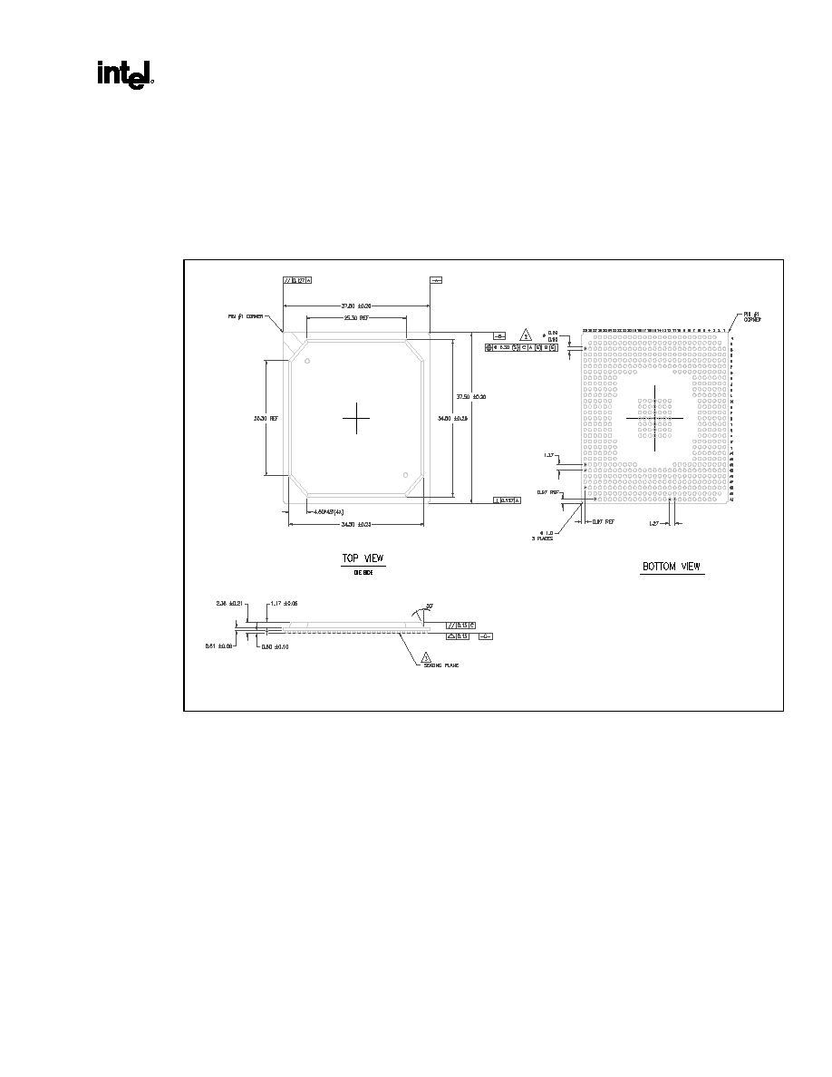
Intel
Æ
830 Chipset Family
298338-003 Datasheet
245
R
7.7
Intel 830 Chipset Family Chipset Package Dimensions
Figure 24 outlines the mechanical dimensions for the Intel 830 Chipset family GMCH-M. The package
is a 625-ball grid array (BGA) package.
Figure 24. Intel 830 Chipset Family GMCH-M Package Dimensions