8XC196KD/8XC196KD20
8XC196KD VERTICAL WINDOWING
MAP
Table 1. 128-Byte Windows
Address to
Device
WSR Contents
Remap
Series
0380H
KD
X001 0111B e 17H
0300H
KD
X001 0110B e 16H
0280H
KD
X001 0101B e 15H
0200H
KD
X001 0100B e 14H
0180H
KC, KD
X001 0011B e 13H
0100H
KC, KD
X001 0010B e 12H
0080H
KC, KD
X001 0001B e 11H
0000H
KC, KD
X001 0000B e 10H
Window in Lower Register File: 80H�FFH
Table 2. 64-Byte Windows
Address to
Device
WSR Contents
Remap
Series
03C0H
KD
X010 1111B e 2FH
0380H
KD
X010 1110B e 2EH
0340H
KD
X010 1101B e 2DH
0300H
KD
X010 1100B e 2CH
02C0H
KD
X010 1011B e 2BH
0280H
KD
X010 1010B e 2AH
0240H
KD
X010 1001B e 29H
0200H
KD
X010 1000B e 28H
01C0H
KC, KD
X010 0111B e 27H
0180H
KC, KD
X010 0110B e 26H
0140H
KC, KD
X010 0101B e 25H
0100H
KC, KD
X010 0100B e 24H
00C0H
KC, KD
X010 0011B e 23H
0080H
KC, KD
X010 0010B e 22H
0040H
KC, KD
X010 0001B e 21H
0000H
KC, KD
X010 0000B e 20H
Window in Lower Register File: C0H�FFH
Table 3. 32-Byte Windows
Address to
Device
WSR Contents
Remap
Series
03E0H
KD
X101 1111B e 5FH
03C0H
KD
X101 1110B e 5EH
03A0H
KD
X101 1101B e 5DH
0380H
KD
X101 1100B e 5CH
0360H
KD
X101 1011B e 5BH
0340H
KD
X101 1010B e 5AH
0320H
KD
X101 1001B e 59H
0300H
KD
X101 1000B e 58H
02E0H
KD
X101 0111B e 57H
02C0H
KD
X101 0110B e 56H
02A0H
KD
X101 0101B e 55H
0280H
KD
X101 0100B e 54H
0260H
KD
X101 0011B e 53H
0240H
KD
X101 0010B e 52H
0220H
KD
X101 0001B e 51H
0200H
KD
X101 0000B e 50H
01E0H
KC, KD
X100 1111B e 4FH
01C0H
KC, KD
X100 1110B e 4EH
01A0H
KC, KD
X100 1101B e 4DH
0180H
KC, KD
X100 1100B e 4CH
0160H
KC, KD
X100 1011B e 4BH
0140H
KC, KD
X100 1010B e 4AH
0120H
KC, KD
X100 1001B e 49H
0100H
KC, KD
X100 1000B e 48H
00E0H
KC, KD
X100 0111B e 47H
00C0H
KC, KD
X100 0110B e 46H
00A0H
KC, KD
X100 0101B e 45H
0080H
KC, KD
X100 0100B e 44H
0060H
KC, KD
X100 0011B e 43H
0040H
KC, KD
X100 0010B e 42H
0020H
KC, KD
X100 0001B e 41H
0000H
KC, KD
X100 0000B e 40H
Window in Lower Register File: E0H�FFH
3
8XC196KD/8XC196KD20
PROCESS INFORMATION
This device is manufactured on PX29.5 or PX29.9, a
CHMOS III process. Additional process and reliabili-
ty information is available in the Intel� Quality
System Handbook:
http://developer.intel.com/design/quality/quality.htm
NOTE:
1. EPROMs are available as One Time Programmable
(OTPROM) only.
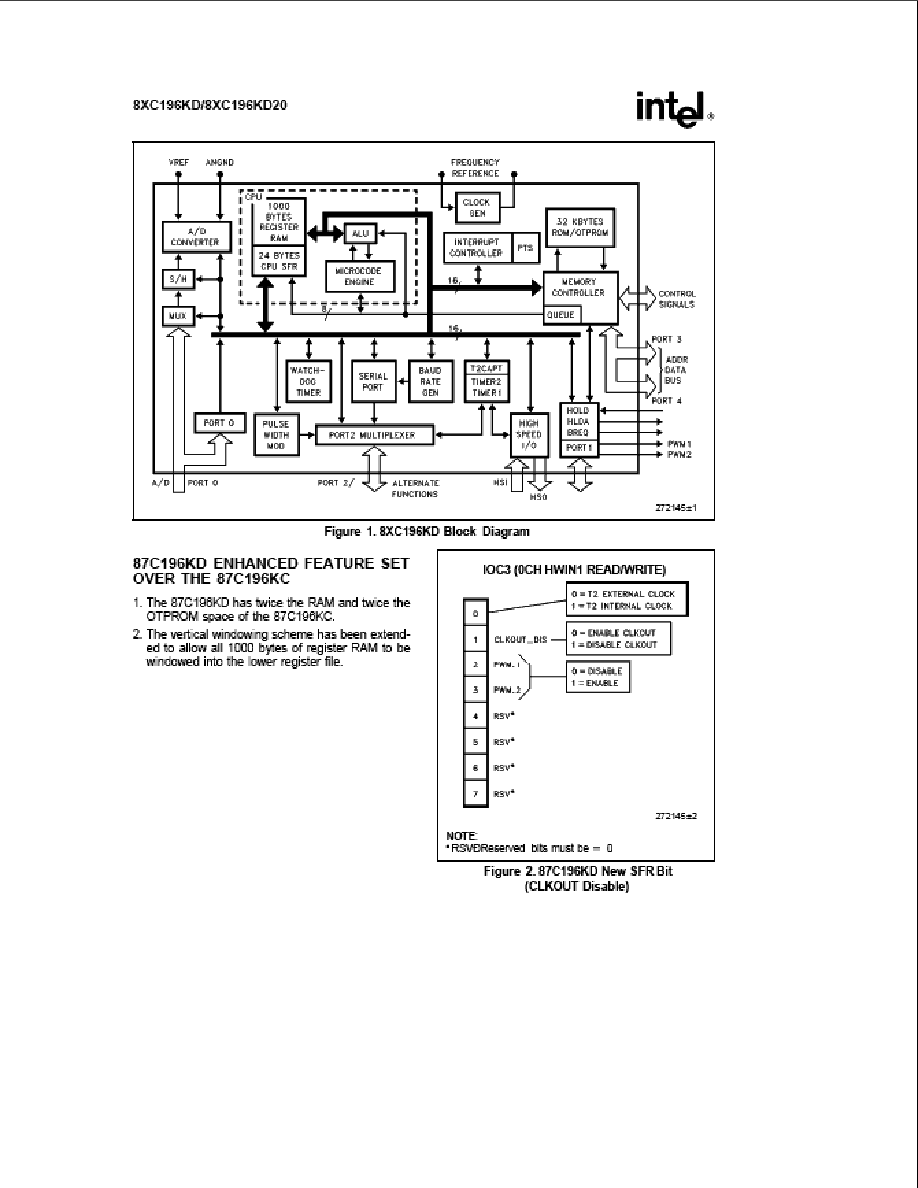
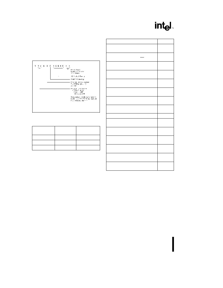
Figure 3. The 8XC196KD Family Nomenclature
Table 4. Thermal Characteristics
Package
ja
jc
Type
PLCC
35
�
C/W
13
�
C/W
QFP
56
�
C/W
12
�
C/W
SQFP
68
�
C/W
15.5
�
C/W
All thermal impedance data is approximate for static air
conditions at 1W of power dissipation. Values will change
depending on operation conditions and application. See
the Intel
Packaging Handbook (order number 240800) for a
description of Intel's thermal impedance test methodology.
Table 5. 8XC196KD Memory Map
Description
Address
External Memory or I/O
0FFFFH
0A000H
Internal ROM/OTPROM or External
9FFFH
Memory (Determined by EA)
2080H
Reserved. Must contain FFH.
207FH
(Note 5)
205EH
PTS Vectors
205DH
2040H
Upper Interrupt Vectors
203FH
2030H
ROM/OTPROM Security Key
202FH
2020H
Reserved. Must contain FFH.
201FH
(Note 5)
201AH
Reserved. Must Contain 20H
2019H
(Note 5)
CCB
2018H
Reserved. Must contain FFH.
2017H
(Note 5)
2014H
Lower Interrupt Vectors
2013H
2000H
Port 3 and Port 4
1FFFH
1FFEH
External Memory
1FFDH
0400H
1000 Bytes Register RAM (Note 1)
03FFH
0018H
CPU SFR's (Notes 1, 3)
0017H
0000H
NOTES:
1. Code executed in locations 0000H to 03FFH will be
forced external.
2. Reserved memory locations must contain 0FFH unless
noted.
3. Reserved SFR bit locations must contain 0.
4. Refer to 8XC196KC for SFR descriptions.
5. WARNING: Reserved memory locations must not be
written or read. The contents and/or function of these lo-
cations may change with future revisions of the device.
Therefore, a program that relies on one or more of these
locations may not function properly.
4
x
x
x
8XC196KD/8XC196KD20
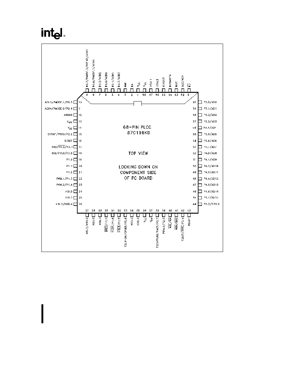
272145�3
Figure 4. 68-Pin PLCC Package
5
8XC196KD/8XC196KD20
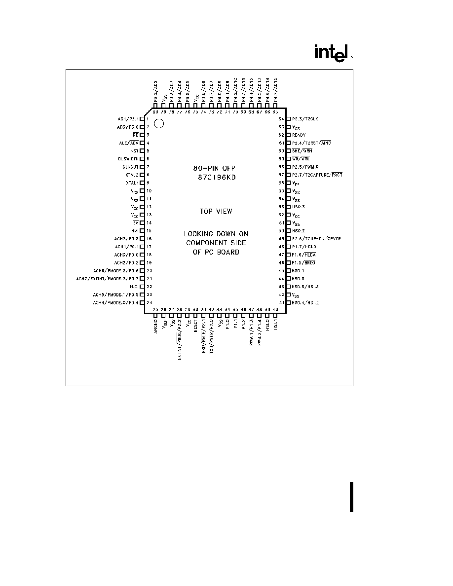
272145�4
NOTE:
N.C. means No Connect (do not connect these pins).
Figure 5. 80-Pin QFP Package
6
8XC196KD/8XC196KD20
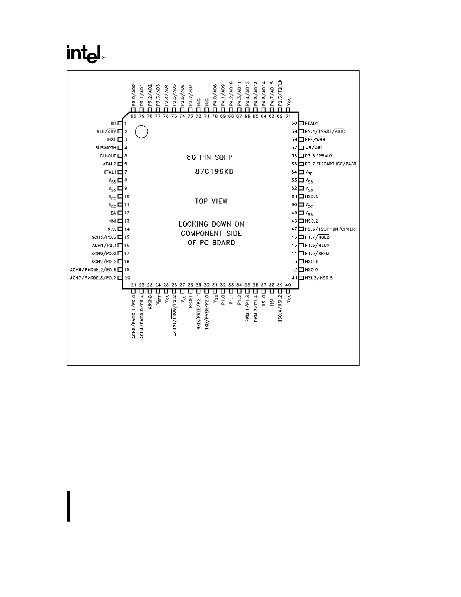
272145�20
NOTE:
N.C. means No Connect (do not connect these pins).
Figure 6. 80-Pin SQFP Package
7
8XC196KD/8XC196KD20
PIN DESCRIPTIONS
Symbol
Name and Function
V
CC
Main supply voltage (5V).
V
SS
Digital circuit ground (0V). There are multiple V
SS
pins, all of which must be connected.
V
REF
Reference voltage for the A/D converter (5V). V
REF
is also the supply voltage to the analog
portion of the A/D converter and the logic used to read Port 0. Must be connected for A/D
and Port 0 to function.
ANGND
Reference ground for the A/D converter. Must be held at nominally the same potential as
V
SS
.
V
PP
Timing pin for the return from powerdown circuit. This pin also supplies the programming
voltage on the EPROM device.
XTAL1
Input of the oscillator inverter and of the internal clock generator.
XTAL2
Output of the oscillator inverter.
CLKOUT
Output of the internal clock generator. The frequency of CLKOUT is
the oscillator
frequency.
RESET
Reset input and open drain output.
BUSWIDTH
Input for buswidth selection. If CCR bit 1 is a one, this pin selects the bus width for the bus
cycle in progress. If BUSWIDTH is a 1, a 16-bit bus cycle occurs. If BUSWIDTH is a 0 an
8-bit cycle occurs. If CCR bit 1 is a 0, the bus is always an 8-bit bus.
NMI
A positive transition causes a vector through 203EH.
INST
Output high during an external memory read indicates the read is an instruction fetch. INST
is valid throughout the bus cycle. INST is activated only during external memory accesses
and output low for a data fetch.
EA
Input for memory select (External Access). EA equal high causes memory accesses to
locations 2000H through 9FFFH to be directed to on-chip ROM/E PROM. EA equal low
causes accesses to those locations to be directed to off-chip memory. Also used to enter
programming mode.
ALE/ADV
Address Latch Enable or Address Valid output, as selected by CCR. Both pin options
provide a signal to demultiplex the address from the address/data bus. When the pin is
ADV, it goes inactive high at the end of the bus cycle. ALE/ADV is activated only during
external memory accesses.
RD
Read signal output to external memory. RD is activated only during external memory reads.
WR/WRL
Write and Write Low output to external memory, as selected by the CCR. WR will go low for
every external write, while WRL will go low only for external writes where an even byte is
being written. WR/WRL is activated only during external memory writes.
BHE/WRH
Bus High Enable or Write High output to external memory, as selected by the CCR. BHE will
go low for external writes to the high byte of the data bus. WRH will go low for external
writes where an odd byte is being written. BHE/WRH is activated only during external
memory writes.
READY
Ready input to lengthen external memory cycles, for interfacing to slow or dynamic
memory, or for bus sharing. When the external memory is not being used, READY has no
effect.
HSI
Inputs to High Speed Input Unit. Four HSI pins are available: HSI.0, HSI.1, HSI.2 and HSI.3.
Two of them (HSI.2 and HSI.3) are shared with the HSO Unit.
HSO
Outputs from High Speed Output Unit. Six HSO pins are available: HSO.0, HSO.1, HSO.2,
HSI.3, HSO.4 and HSO.5. Two of them (HSO.4 and HSO.5) are shared with the HSI Unit.
8
8XC196KD/8XC196KD20
PIN DESCRIPTIONS
(Continued)
Symbol
Name and Function
Port 0
8-bit high impedance input-only port. These pins can be used as digital inputs and/or as
analog inputs to the on-chip A/D converter.
Port 1
8-bit quasi-bidirectional I/O port.
Port 2
8-bit multi-functional port. All of its pins are shared with other functions in the 8XC196KD.
Pins 2.6 and 2.7 are quasi-bidirectional.
Ports 3 and 4
8-bit bidirectional I/O ports with open drain outputs. These pins are shared with the
multiplexed address/data bus which has strong internal pullups.
HOLD
Bus Hold input requesting control of the bus.
HLDA
Bus Hold acknowledge output indicating release of the bus.
BREQ
Bus Request output activated when the bus controller has a pending external memory
cycle.
PMODE
Determines the EPROM programming mode.
PACT
A low signal in Auto Programming mode indicates that programming is in process. A high
signal indicates programming is complete.
PALE
A falling edge in Slave Programming Mode and Auto Configuration Byte Programming
Mode indicates that ports 3 and 4 contain valid programming address/command
information (input to slave).
PROG
A falling edge in Slave Programming Mode indicates that ports 3 and 4 contain valid
programming data (input to slave).
PVER
A high signal in Slave Programming Mode and Auto Configuration Byte Programming
Mode indicates the byte programmed correctly.
CPVER
Cummulative Program Output Verification. Pin is high if all locations have programmed
correctly since entering a programming mode.
AINC
Auto Increment. Active low input enables the auto increment mode. Auto increment allows
reading or writing sequential EPROM locations without address transactions across the
PBUS for each read or write.
9
8XC196KD/8XC196KD20
ELECTRICAL CHARACTERISTICS
ABSOLUTE MAXIMUM RATINGS
Ambient Temperature
Under Bias.................................b 55 C to a125 C
Storage Temperature....................b 65 C to a150 C
Voltage On Any Pin to V
SS
Except EA and V
PP
...................b0.5V to a7.0V
(1)
Voltage from EA or
V
PP
to V
SS
or ANGND..............b0.5V to a13.00V
Power Dissipation............................................1.5W
(2)
NOTES:
1. This includes V
PP
and EA on ROM or CPU only devices.
2. Power dissipation is based on package heat transfer lim-
itations, not device power consumption.
NOTICE: This data sheet contains information on
products in the sampling and initial production phases
of development. It is valid for the devices indicated in
the revision history. The specifications are subject to
change without notice.
WARNING: Stressing the device beyond the ``Absolute
Maximum Ratings'' may cause permanent damage.
These are stress ratings only. Operation beyond the
``Operating Conditions'' is not recommended and ex-
tended exposure beyond the ``Operating Conditions''
may affect device reliability.
OPERATING CONDITIONS
Symbol Description Min Max Units
T
A
Ambient Temperature Under Bias
Commercial
Temp.
0
a
70
C
V
CC
Digital Supply Voltage
4.50
5.50
V
V
REF
Analog Supply Voltage
4.00
5.50
V
ANGND
Analog Ground Voltage
V
SS
b
0.4
V
SS
a
0.4
V
(1)
F
OSC
Oscillator Frequency (
8XC196KD
)
8
16
MHz
F
OSC
Oscillator Frequency (
8XC196KD20
)
8
20
MHz
NOTE:
1. ANGND and V
SS
should be nominally at the same potential.
DC CHARACTERISTICS
(Over Specified Operating Conditions)
Symbol Description Min Max Units Test Conditions
V
IL
Input Low Voltage
b
0.5
0.8
V
V
IH
Input High Voltage (Note 1)
0.2 V
CC
a
1.0
V
CC
a
0.5
V
V
HYS
Hysteresis on RESET
300
mV
V
CC
e
5.0V
V
IH1
Input High Voltage on XTAL 1
0.7 V
CC
V
CC
a
0.5
V
V
IH2
Input High Voltage on RESET
2.2
V
CC
a
0.5
V
V
OL
Output Low Voltage
0.3
V
I
OL
e
200 mA
0.45
V
I
OL
e
2.8 mA
1.5
V
I
OL
e
7 mA
V
OL1
Output Low Voltage
0.8
V
I
OL
e a
0.4 mA
in RESET on P2.5 (Note 2)
V
OH
Output High Voltage
V
CC
b
0.3
V
I
OH
e b
200 mA
(Standard Outputs) (Note 4)
V
CC
b
0.7
V
I
OH
e b
3.2 mA
V
CC
b
1.5
V
I
OH
e b
7 mA
V
OH1
Output High Voltage
V
CC
b
0.3
V
I
OH
e b
10 mA
(Quasi-bidirectional Outputs)
V
CC
b
0.7
V
I
OH
e b
30 mA
(Note 3)
V
CC
b
1.5
V
I
OH
e b
60 mA
10
T
A
Ambient Temperature Under Bias
Extended Temp. -40 +85 �C

8XC196KD/8XC196KD20
DC CHARACTERISTICS
(Over Specified Operating Conditions) (Continued)
Symbol Description Min Typ Max Units Test Conditions
I
OH1
Logical 1 Output Current in Reset
b
0.8
mA
V
IH
e
V
CC
b
1.5V
on P2.0. Do not exceed this or
device may enter test modes.
I
IL2
Logical 0 Input Current in Reset
b
12.0
mA
V
IN
e
0.45V
on P2.0. Maximum current that
must be sunk by external device
to ensure test mode entry.
I
IH1
Logical 1 Input Current. Maximum
a
200
m
A
V
IN
e
2.4V
current that external device must
source to initiate NMI.
I
LI
Input Leakage Current (Std.
g
10
m
A
0
k
V
IN k
V
CC
b
0.3V
Inputs) (Note 5)
I
LI1
Input Leakage Current (Port 0)
g
3
m
A
0
k
V
IN k
V
REF
I
TL
1 to 0 Transition Current (QBD
b
650
m
A
V
IN
e
2.0V
Pins)
I
IL
Logical 0 Input Current (QBD Pins)
b
70
m
A
V
IN
e
0.45V
I
IL1
AD Bus in Reset
b
70
m
A
V
IN
e
0.45V
I
CC
Active Mode Current in Reset
65
75
mA
XTAL1 e 16 MHz
(
8XC196KD
)
V
CC
e
V
PP
e
V
REF
e
5.5V
I
CC
Active Mode Current in Reset
80
92
mA
XTAL1 e 20 MHz
(
8XC196KD20
)
V
CC
e
V
PP
e
V
REF
e
5.5V
I
IDLE
Idle Mode Current (
8XC196KD
)
17
25
mA
XTAL1 e 16 MHz
V
CC
e
V
PP
e
V
REF
e
5.5V
I
IDLE
Idle Mode Current (
8XC196KD20
)
21
30
mA
XTAL1 e 20 MHz
V
CC
e
V
PP
e
V
REF
e
5.5V
I
PD
Powerdown Mode Current
8
15
m
A
V
CC
e
V
PP
e
V
REF
e
5.5V
I
REF
A/D Converter Reference Current
2
5
mA
V
CC
e
V
PP
e
V
REF
e
5.5V
R
RST
Reset Pullup Resistor
6K
65K
X
V
CC
e
5.5V, V
IN
e
4.0V
C
S
Pin Capacitance (Any Pin to V
SS
)
10
pF
NOTES:
1. All pins except RESET and XTAL1.
2. Violating these specifications in Reset may cause the part to enter test modes.
3. QBD (Quasi-bidirectional) pins include Port 1, P2.6 and P2.7.
4. Standard Outputs include AD0�15, RD, WR, ALE, BHE, INST, HSO pins, PWM/P2.5, CLKOUT, RESET, Ports 3 and 4,
TXD/P2.0 and RXD (in serial mode 0). The V
OH
specification is not valid for RESET. Ports 3 and 4 are open-drain outputs.
5. Standard Inputs include HSI pins, READY, BUSWIDTH, RXD/P2.1, EXTINT/P2.2, T2CLK/P2.3 and T2RST/P2.4.
6. Maximum current per pin must be externally limited to the following values if V
OL
is held above 0.45V or V
OH
is held
below V
CC
b
0.7V:
I
OL
on Output pins: 10 mA
I
OH
on quasi-bidirectional pins: self limiting
I
OH
on Standard Output pins: 10 mA
7. Maximum current per bus pin (data and control) during normal operation is
g
3.2 mA.
8. During normal (non-transient) conditions the following total current limits apply:
Port 1, P2.6
I
OL
: 29 mA
I
OH
is self limiting
HSO, P2.0, RXD, RESET I
OL
: 29 mA
I
OH
: 26 mA
P2.5, P2.7, WR, BHE
I
OL
: 13 mA
I
OH
: 11 mA
AD0�AD15
I
OL
: 52 mA
I
OH
: 52 mA
RD, ALE, INST�CLKOUT I
OL
: 13 mA
I
OH
: 13 mA
11
8XC196KD/8XC196KD20
272145�5
I
CC
Max
e
4.13
c
Frequency
a
9 mA
I
CC
Typ
e
3.50
c
Frequency
a
9 mA
I
IDLE
Max
e
1.25
c
Frequency
a
5 mA
I
IDLE
Typ
e
0.88
c
Frequency
a
3 mA
NOTE:
Frequencies below 8 MHz are shown for reference only; no testing is performed.
Figure 7. I
CC
and I
IDLE
vs Frequency
AC CHARACTERISTICS
For use over specified operating conditions.
Test Conditions: Capacitive load on all pins e 100 pF, Rise and fall times e 10 ns, F
OSC
e
16/20 MHz
The system must meet these specifications to work with the 80C196KD:
Symbol
Description
Min
Max
Units
Notes
T
AVYV
Address Valid to READY Setup
2 T
OSC
b
68
ns
T
YLYH
Non READY Time
No upper limit
ns
T
CLYX
READY Hold after CLKOUT Low
0
T
OSC
b
30
ns
(Note 1)
T
LLYX
READY Hold after ALE Low
T
OSC
b
15
2 T
OSC
b
40
ns
(Note 1)
T
AVGV
Address Valid to Buswidth Setup
2 T
OSC
b
68
ns
T
CLGX
Buswidth Hold after CLKOUT Low
0
ns
T
AVDV
Address Valid to Input Data Valid
3 T
OSC
b
55
ns
(Note 2)
T
RLDV
RD Active to Input Data Valid
T
OSC
b
22
ns
(Note 2)
T
CLDV
CLKOUT Low to Input Data Valid
T
OSC
b
45
ns
T
RHDZ
End of RD to Input Data Float
T
OSC
ns
T
RXDX
Data Hold after RD Inactive
0
ns
NOTES:
1. If max is exceeded, additional wait states will occur.
2. If wait states are used, add 2 T
OSC
N, where N
e
number of wait states.
12
8XC196KD/8XC196KD20
AC CHARACTERISTICS
(Continued)
For use over specified operating conditions.
Test Conditions: Capacitive load on all pins e 100 pF, Rise and fall times e 10 ns, F
OSC
e
16/20 MHz
The 80C196KD will meet these specifications:
Symbol
Description
Min
Max
Units
Notes
F
XTAL
Frequency on XTAL1 (
8XC196KD
)
8
16
MHz
(Note 1)
F
XTAL
Frequency on XTAL1 (
8XC196KD20
)
8
20
MHz
(Note 1)
T
OSC
I/F
XTAL
(
8XC196KD
)
62.5
125
ns
T
OSC
I/F
XTAL
(
8XC196KD20
)
50
125
ns
T
XHCH
XTAL1 High to CLKOUT High or Low
a
20
a
110
ns
T
CLCL
CLKOUT Cycle Time
2 T
OSC
ns
T
CHCL
CLKOUT High Period
T
OSC
b
10
T
OSC
a
15
ns
T
CLLH
CLKOUT Falling Edge to ALE Rising
b
5
a
15
ns
T
LLCH
ALE Falling Edge to CLKOUT Rising
b
20
a
15
ns
T
LHLH
ALE Cycle Time
4 T
OSC
ns
(Note 4)
T
LHLL
ALE High Period
T
OSC
b
10
T
OSC
a
10
ns
T
AVLL
Address Setup to ALE Falling Edge
T
OSC
b
15
T
LLAX
Address Hold after ALE Falling Edge
T
OSC
b
35
ns
T
LLRL
ALE Falling Edge to RD Falling Edge
T
OSC
b
30
ns
T
RLCL
RD Low to CLKOUT Falling Edge
a
4
a
30
ns
T
RLRH
RD Low Period
T
OSC
b
5
ns
(Note 4)
T
RHLH
RD Rising Edge to ALE Rising Edge
T
OSC
T
OSC
a
25
ns
(Note 2)
T
RLAZ
RD Low to Address Float
a
5
ns
T
LLWL
ALE Falling Edge to WR Falling Edge
T
OSC
b
10
ns
T
CLWL
CLKOUT Low to WR Falling Edge
0
a
25
ns
T
QVWH
Data Stable to WR Rising Edge
T
OSC
b
23
(Note 4)
T
CHWH
CLKOUT High to WR Rising Edge
b
5
a
15
ns
T
WLWH
WR Low Period
T
OSC
b
20
ns
(Note 4)
T
WHQX
Data Hold after WR Rising Edge
T
OSC
b
25
ns
T
WHLH
WR Rising Edge to ALE Rising Edge
T
OSC
b
10
T
OSC
a
15
ns
(Note 2)
T
WHBX
BHE, INST after WR Rising Edge
T
OSC
b
10
ns
T
WHAX
AD8�15 HOLD after WR Rising
T
OSC
b
30
ns
(Note 3)
T
RHBX
BHE, INST after RD Rising Edge
T
OSC
b
10
ns
T
RHAX
AD8�15 HOLD after RD Rising
T
OSC
b
25
ns
(Note 3)
NOTES:
1. Testing performed at 8 MHz. However, the device is static by design and will typically operate below 1 Hz.
2. Assuming back-to-back bus cycles.
3. 8-Bit bus only.
4. If wait states are used, add 2 T
OSC
N, where N
e
number of wait states.
13
8XC196KD/8XC196KD20
System Bus Timings
272145�6
14
8XC196KD/8XC196KD20
READY Timings (One Wait State)
272145�7
Buswidth Timings
272145�8
15
8XC196KD/8XC196KD20
HOLD/HLDA TIMINGS
Symbol
Description Min Max Units Notes
T
HVCH
HOLD Setup
a
55
ns
(Note 1)
T
CLHAL
CLKOUT Low to HLDA Low
b
15
a
15
ns
T
CLBRL
CLKOUT Low to BREQ Low
b
15
a
15
ns
T
HALAZ
HLDA Low to Address Float
a
15
ns
T
HALBZ
HLDA Low to BHE, INST, RD, WR Weakly Driven
a
20
ns
T
CLHAH
CLKOUT Low to HLDA High
b
15
a
15
ns
T
CLBRH
CLKOUT Low to BREQ High
b
15
a
15
ns
T
HAHAX
HLDA High to Address No Longer Float
b
15
ns
T
HAHBV
HLDA High to BHE, INST, RD, WR Valid
b
10
a
15
ns
T
CLLH
CLKOUT Low to ALE High
b
5
a
15
ns
NOTE:
1. To guarantee recognition at next clock.
DC SPECIFICATIONS IN HOLD
Description
Min
Max
Units
Weak Pullups on ADV, RD,
50K
250K
V
CC
e
5.5V, V
IN
e
0.45V
WR, WRL, BHE
Weak Pulldowns on ALE, INST
10K
50K
V
CC
e
5.5V, V
IN
e
2.4
272145�9
16
8XC196KD/8XC196KD20
MAXIMUM HOLD LATENCY
Bus Cycle Type
Internal Execution
1.5 States
16-Bit External Execution
2.5 States
8-Bit External Execution
4.5 States
EXTERNAL CLOCK DRIVE (8XC196KD)
Symbol Parameter Min Max Units
1/T
XLXL
Oscillator Frequency
8
16.0
MHz
T
XLXL
Oscillator Period
62.5
125
ns
T
XHXX
High Time
20
ns
T
XLXX
Low Time
20
ns
T
XLXH
Rise Time
10
ns
T
XHXL
Fall Time
10
ns
EXTERNAL CLOCK DRIVE (8XC196KD20)
Symbol Parameter Min Max Units
1/T
XLXL
Oscillator Frequency
8
20.0
MHz
T
XLXL
Oscillator Period
50
125
ns
T
XHXX
High Time
17
ns
T
XLXX
Low Time
17
ns
T
XLXH
Rise Time
8
ns
T
XHXL
Fall Time
8
ns
EXTERNAL CLOCK DRIVE WAVEFORMS
272145�10
17
8XC196KD/8XC196KD20
EXTERNAL CRYSTAL CONNECTIONS
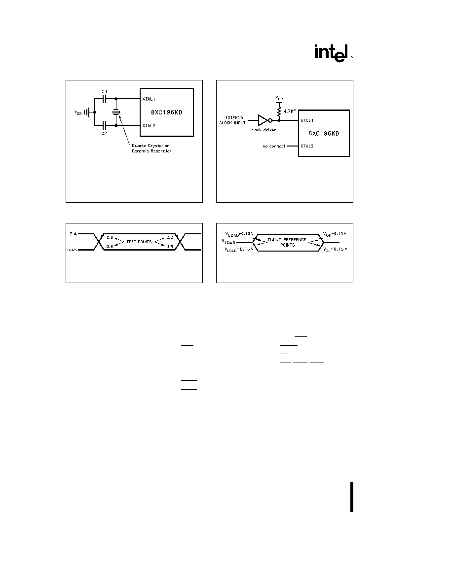
272145�13
NOTE:
Keep oscillator components close to chip and use
short, direct traces to XTAL1, XTAL2 and V
SS
. When
using ceramic crystals, C1
e
20 pF, C2
e
20 pF.
When using ceramic resonators consult manufacturer
for recommended capacitor values.
EXTERNAL CLOCK CONNECTIONS
272145�14
NOTE:
Required if TTL driver used.
Not needed if CMOS driver is used.
AC TESTING INPUT, OUTPUT WAVEFORMS
272145�11
AC Testing inputs are driven at 2.4V for a Logic ``1'' and 0.45V for
a Logic ``0'' Timing measurements are made at 2.0V for a Logic
``1'' and 0.8V for a Logic ``0''.
FLOAT WAVEFORMS
272145�12
For Timing Purposes a Port Pin is no Longer Floating when a
150 mV change from Load Voltage Occurs, and Begins to Float
when a 150 mV change from the Loaded V
OH
/V
OL
Level occurs;
I
OL
/I
OH
e
g
15 mA.
EXPLANATION OF AC SYMBOLS
Each symbol is two pairs of letters prefixed by ``T'' for time. The characters in a pair indicate a signal and its
condition, respectively. Symbols represent the time between the two signal/condition points.
Conditions:
H - High
L - Low
V - Valid
X - No Longer Valid
Z - Floating
Signals:
A - Address
B - BHE
C - CLKOUT
D - DATA
G - Buswidth
H - HOLD
HA - HLDA
L - ALE/ADV
BR - BREQ
R - RD
W - WR/WRH /WRL
X - XTAL1
Y - READY
Q - Data Out
18
8XC196KD/8XC196KD20
AC CHARACTERISTICS-SERIAL PORT-SHIFT REGISTER MODE
SERIAL PORT TIMING-SHIFT REGISTER MODE (MODE0)
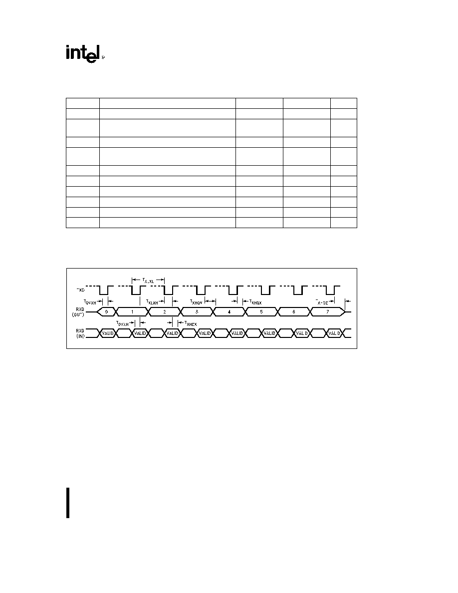
Symbol Parameter Min Max Units
T
XLXL
Serial Port Clock Period (BRR
t
8002H)
6 T
OSC
ns
T
XLXH
Serial Port Clock Falling Edge
4 T
OSC
b
50
4 T
OSC
a
50
ns
to Rising Edge (BRR
t
8002H)
T
XLXL
Serial Port Clock Period (BRR e 8001H)
4 T
OSC
ns
T
XLXH
Serial Port Clock Falling Edge
2 T
OSC
b
50
2 T
OSC
a
50
ns
to Rising Edge (BRR e 8001H)
T
QVXH
Output Data Valid to Clock Rising Edge
2 T
OSC
b
50
ns
T
XHQX
Output Data Hold after Clock Rising Edge
2 T
OSC
b
50
ns
T
XHQV
Next Output Data Valid after Clock Rising Edge
2 T
OSC
a
50
ns
T
DVXH
Input Data Setup to Clock Rising Edge
T
OSC
a
50
ns
T
XHDX
Input Data Hold after Clock Rising Edge
0
ns
T
XHQZ
Last Clock Rising to Output Float
1 T
OSC
ns
WAVEFORM-SERIAL PORT-SHIFT REGISTER MODE
SERIAL PORT WAVEFORM-SHIFT REGISTER MODE (MODE 0)
272145�15
19
8XC196KD/8XC196KD20
A to D CHARACTERISTICS
The A/D converter is ratiometric, so absolute accuracy is dependent on the accuracy and stability of V
REF
.
10-BIT MODE A/D OPERATING CONDITIONS
Symbol
Description
Min
Max
Units
T
A
Ambient Temperature
Commercial
Temp.
0
a
70
C
V
CC
Digital Supply Voltage
4.50
5.50
V
V
REF
Analog Supply Voltage
4.00
5.50
V
ANGND
Analog Ground Voltage
V
SS
b
0.40
V
CC
a
0.40
V
T
SAM
Sample Time
1.0
m
s
(1)
T
CONV
Conversion Time
10
20
m
s
(1)
F
OSC
Oscillator Frequency (
8XC196KD
)
8.0
16.0
MHz
F
OSC
Oscillator Frequency (
8XC196KD20
)
8.0
20.0
MHz
NOTE:
1. The value of AD_TIME is selected to meet these specifications.
10-BIT MODE A/D CHARACTERISTICS
(Over Specified Operating Conditions)
Parameter Typical
(1)
Minimum Maximum Units
*
Notes
Resolution
1024
1024
Levels
10
10
Bits
Absolute Error
0
g
3
LSBs
Full Scale Error
0.25
g
0.5
LSBs
Zero Offset Error
0.25
g
0.5
LSBs
Non-Linearity
1.0
g
2.0
0
g
3
LSBs
Differential Non-Linearity Error
l
b
1
a
2
LSBs
Channel-to-Channel Matching
g
0.1
0
g
1
LSBs
Repeatability
g
0.25
LSBs
Temperature Coefficients:
Offset
0.009
LSB/ C
Full Scale
0.009
LSB/ C
Differential Non-Linearity
0.009
LSB/ C
Off Isolation
b
60
dB
2, 3
Feedthrough
b
60
dB
2
V
CC
Power Supply Rejection
b
60
dB
2
Input Series Resistance
750
1.2K
X
4
Voltage on Analog Input Pin
ANGND b 0.5
V
REF
a
0.5
V
5, 6
DC Input Leakage
0
g
3.0
m
A
Sampling Capacitor
3
pF
NOTES:
An ``LSB'' as used here has a value of approxiimately 5 mV. (See Embedded Microcontrollers and Processors Handbook
for A/D glossary of terms.)
1. These values are expected for most parts at 25 C but are not tested or guaranteed.
2. DC to 100 KHz.
3. Multiplexer Break-Before-Make is guaranteed.
4. Resistance from device pin, through internal MUX, to sample capacitor.
5. These values may be exceeded if the pin current is limited to
g
2 mA.
6. Applying voltages beyond these specifications will degrade the accuracy of other channels being converted.
7. All conversions performed with processor in IDLE mode.
20
T
A
Ambient Temperature
Extended Temp. -40 +85 �C
8XC196KD/8XC196KD20
8-BIT MODE A/D OPERATING CONDITIONS
Symbol
Description
Min
Max
Units
T
A
Ambient Temperature
Commercial
Temp.
0
a
70
C
V
CC
Digital Supply Voltage
4.50
5.50
V
V
REF
Analog Supply Voltage
4.00
5.50
V
ANGND
Analog Ground Voltage
V
SS
b
0.40
V
SS
a
0.40
V
T
SAM
Sample Time
1.0
m
s
(1)
T
CONV
Conversion Time
7
20
m
s
(1)
F
OSC
Oscillator Frequency (
8XC196KD
)
8.0
16.0
MHz
F
OSC
Oscillator Frequency (
8XC196KD20
)
8.0
20.0
MHz
NOTE:
1. The value of AD_TIME is selected to meet these specifications.
8-BIT MODE A/D CHARACTERISTICS
(Over Specified Operating Conditions)
Parameter Typical
(1)
Minimum Maximum Units*
Notes
Resolution
256
256
Levels
8
8
Bits
Absolute Error
0
g
1
LSBs
Full Scale Error
g
0.5
LSBs
Zero Offset Error
g
0.5
LSBs
Non-Linearity
0
g
1
LSBs
Differential Non-Linearity Error
l
b
1
a
1
LSBs
Channel-to-Channel Matching
g
1
LSBs
Repeatability
g
0.25
LSBs
Temperature Coefficients:
Offset
0.003
LSB/ C
Full Scale
0.003
LSB/ C
Differential Non-Linearity
0.003
LSB/ C
Off Isolation
b
60
dB
2, 3
Feedthrough
b
60
dB
2
V
CC
Power Supply Rejection
b
60
dB
2
Input Series Resistance
750
1.2K
X
4
Voltage on Analog Input Pin
V
SS
b
0.5
V
REF
a
0.5
V
5, 6
DC Input Leakage
0
g
3.0
m
A
Sampling Capacitor
3
pF
NOTES:
An ``LSB'' as used here has a value of approximately 20 mV. (See Embedded Microcontrollers and Processors Handbook
for A/D glossary of terms).
1. These values are expected for most parts at 25 C but are not tested or guaranteed.
2. DC to 100 KHz.
3. Multiplexer Break-Before-Make is guaranteed.
4. Resistance from device pin, through internal MUX, to sample capacitor.
5. These values may be exceeded if pin current is limited to
g
2 mA.
6. Applying voltages beyond these specifications will degrade the accuracy of other channels being converted.
7. All conversions performed with processor in IDLE mode.
21
T
A
Ambient Temperature
Extended Temp. -40 +85 �C
8XC196KD/8XC196KD20
OTPROM SPECIFICATIONS
OPERATING CONDITIONS
Symbol Description Min Max Units
T
A
Ambient Temperature During Programming
20
30
C
V
CC
Supply Voltage During Programming
4.5
5.5
V
(1)
V
REF
Reference Supply Voltage During Programming
4.5
5.5
V
(1)
V
PP
Programming Voltage
12.25
12.75
V
(2)
V
EA
EA Pin Voltage
12.25
12.75
V
(2)
F
OSC
Oscillator Frequency during Auto and Slave
6.0
8.0
MHz
Mode Programming
F
OSC
Oscillator Frequency during
6.0
16.0
MHz
Run-Time Programming (
8XC196KD
)
F
OSC
Oscillator Frequency during
6.0
20.0
MHz
Run-Time Programming (
8XC196KD20
)
NOTES:
1. V
CC
and V
REF
should nominally be at the same voltage during programming.
2. V
PP
and V
EA
must never exceed the maximum specification, or the device may be damaged.
3. V
SS
and ANGND should nominally be at the same potential (0V).
4. Load capacitance during Auto and Slave Mode programming
e
150 pF.
AC OTPROM PROGRAMMING CHARACTERISTICS (SLAVE MODE)
Symbol Description Min Max Units
T
SHLL
Reset High to First PALE Low
1100
T
OSC
T
LLLH
PALE Pulse Width
50
T
OSC
T
AVLL
Address Setup Time
0
T
OSC
T
LLAX
Address Hold Time
100
T
OSC
T
PLDV
PROG Low to Word Dump Valid
50
T
OSC
T
PHDX
Word Dump Data Hold
50
T
OSC
T
DVPL
Data Setup Time
0
T
OSC
T
PLDX
Data Hold Time
400
T
OSC
T
PLPH(1)
PROG Pulse Width
50
T
OSC
T
PHLL
PROG High to Next PALE Low
220
T
OSC
T
LHPL
PALE High to PROG Low
220
T
OSC
T
PHPL
PROG High to Next PROG Low
220
T
OSC
T
PHIL
PROG High to AINC Low
0
T
OSC
T
ILIH
AINC Pulse Width
240
T
OSC
T
ILVH
PVER Hold after AINC Low
50
T
OSC
T
ILPL
AINC Low to PROG Low
170
T
OSC
T
PHVL
PROG High to PVER Valid
220
T
OSC
NOTE:
1. This specification is for the Word Dump Mode. For programming pulses, use the Modified Quick Pulse Algorithm.
22
8XC196KD/8XC196KD20
DC OTPROM PROGRAMMING CHARACTERISTICS
Symbol Description Min Max Units
I
PP
V
PP
Supply Current (When Programming)
100
mA
NOTE:
Do not apply V
PP
until V
CC
is stable and within specifications and the oscillator/clock has stabilized or the device may be
damaged.
OTPROM PROGRAMMING WAVEFORMS
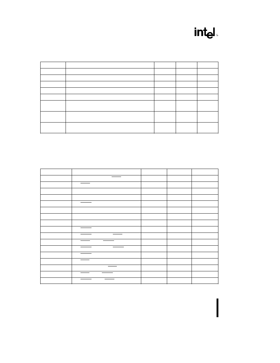
SLAVE PROGRAMMING MODE DATA PROGRAM MODE WITH SINGLE PROGRAM PULSE
272145�16
NOTE:
P3.0 must be high (``1'')
23
8XC196KD/8XC196KD20
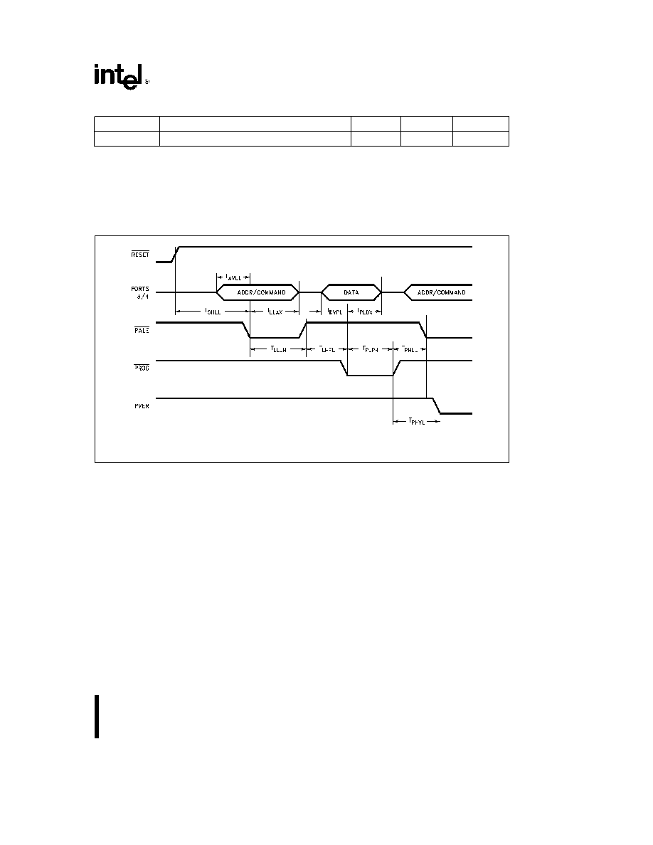
SLAVE PROGRAMMING MODE IN WORD DUMP WITH AUTO INCREMENT
272145�17
NOTE:
P3.0 must be low (``0'')
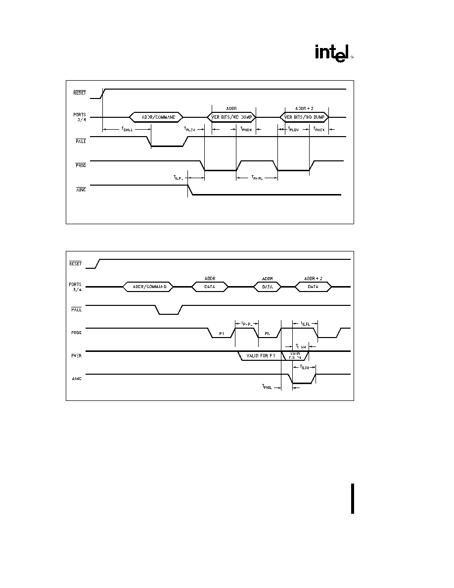
SLAVE PROGRAMMING MODE TIMING IN DATA PROGRAM WITH REPEATED PROG PULSE AND
AUTO INCREMENT
272145�18
24

8XC196KD/8XC196KD20
8XC196KC TO 8XC196KD DESIGN
CONSIDERATIONS
1. Memory Map. The 8XC196KD has 1024 bytes of
RAM/SFRs and 32K of OTPROM. The extra 512
bytes of RAM reside in locations 0200H to
03FFH, and the extra 16 Kbytes of OTPROM re-
side in locations 6000H to 9FFFH. On the
87C196KC these locations are always external,
so KC code may have to be modified to run on
the KD.
2. The vertical window scheme has been extended
to include all on-chip RAM.
3. IOC3.1 controls the CLKOUT signal. This bit must
be 0 to enable CLKOUT.
4. The 87C196KD has a different autoprogramming
algorithm to support 32K of on-chip OTPROM.
8XC196KD ERRATA
1. 83C196KD can possibly miss interrupts on P0.7.
See techbit MC0893.
DATA SHEET REVISION HISTORY
This data sheet is valid for devices with a ``D'' and
``E'' at the end of the topside tracking number. Data
sheets are changed as new device information be-
comes available. Verify with your local Intel sales
office that you have the latest version before finaliz-
ing a design or ordering devices.
The following are important differences between the
272145-004 and 272145-005 datasheets:
1. Package prefix variables have been changed.
Variables are now indicated with an "x".
The following are important differences between the
272145-002 and 272145-003 data sheets:
1. I
IL1
specification (logic 0 input current in reset)
was misnamed. It is renamed I
IL2
.
2. T
LLYV
and T
LLGV
were removed. These specifi-
cations are not necessary for high-speed system
designs.
3. An errata with 83C196KD P0.7 EXTINT was add-
ed to the errata section.
The following are important differences between the
272145-001 and 272145-002 data sheets:
1. Added 20 MHz specifications.
2. Added 80-lead SQFP package pinout.
3. Changed QFP Package i
JA
to 56 C/W from
42 C/W.
4. Changed V
HYS
to 300 mV from 150 mV.
5. Changed I
CC
Typical specification at 16 MHz to
65 mA from 50 mA.
6. Changed I
CC
Maximum specification at 16 MHz
to 75 mA from 70 mA.
7. Changed I
IDLE
Typical specification to 17 mA
from 15 mA.
8. Changed I
IDLE
Maximum specification to 25 mA
from 30 mA.
9. Changed I
PD
Typical specification to 8 mA from
15 mA.
10. Added I
PD
Maximum specification.
11. Changed T
CLDV
Maximum specification to
T
OSC
b
45 from T
OSC
b
50.
12. Changed T
LLAX
Minimum specification to
T
OSC
b
35 from T
OSC
b
40.
13. Changed T
CHWH
Minimum specification to b5
from b10.
14. Changed T
RHAX
Minimum specification to
T
OSC
b
25 from T
OSC
b
30.
15. Changed T
HALAZ
Maximum specification to
a
15 from a10.
16. Changed T
HALBZ
Maximum specification to
a
20 from a15.
17. Added T
HAHBV
Maximum specification.
18. Changed T
SAM
for 10-bit mode to 1 ms from
3 ms.
19. Changed T
SAM
for 8-bit mode to 1 ms from 2 ms.
20. Changed I
IH1
test condition to V
IN
e
2.4V from
5.5V.
21. Changed I
IH1
maximum specification to a200
m
A from a100 mA.
22. Removed NMI from list of standard inputs.
23. Updated I
CC
and I
IDLE
vs frequency graph.
24. Updated note under DC EPROM Programming
Characteristics.
25. Changed I
LI1
maximum specification to b12
mA from b6 mA.
25