 | –≠–ª–µ–∫—Ç—Ä–æ–Ω–Ω—ã–π –∫–æ–º–ø–æ–Ω–µ–Ω—Ç: 83C51GB | –°–∫–∞—á–∞—Ç—å:  PDF PDF  ZIP ZIP |

Other brands and names are the property of their respective owners
Information in this document is provided in connection with Intel products Intel assumes no liability whatsoever including infringement of any patent or
copyright for sale and use of Intel products except as provided in Intel's Terms and Conditions of Sale for such products Intel retains the right to make
changes to these specifications at any time without notice Microcomputer Products may have minor variations to this specification known as errata
November 1994
COPYRIGHT
INTEL CORPORATION 1995
Order Number 272337-002
8XC51GB
CHMOS SINGLE-CHIP 8-BIT MICROCONTROLLER
Commercial Express
87C51GB
8 Kbytes OTP 8 Kbytes Internal Program Memory
83C51GB
8 Kbytes Factory Programmable ROM
80C51GB
CPU with RAM and I O
8XC51GB
3 5 MHz to 12 MHz
g
20% V
CC
8XC51GB-1
3 5 MHz to 16 MHz
g
20% V
CC
Y
8 Kbytes On-Chip ROM OTP ROM
Y
256 Bytes of On-Chip Data RAM
Y
Two Programmable Counter Arrays
with
2 x 5 High Speed Input Output
Channels Compare Capture
Pulse Width Modulators
Watchdog Timer Capabilities
Y
Three 16-Bit Timer Counters with
Four Programmable Modes
Capture Baud Rate Generation
(Timer 2)
Y
Dedicated Watchdog Timer
Y
8-Bit 8-Channel A D with
Eight 8-Bit Result Registers
Four Programmable Modes
Y
Programmable Serial Channel with
Framing Error Detection
Automatic Address Recognition
Y
Serial Expansion Port
Y
Programmable Clock Out
Y
Extended Temperature Range
(
b
40 C to
a
85 C)
Y
48 Programmable I O Lines with
40 Schmitt Trigger Inputs
Y
15 Interrupt Sources with
7 External 8 Internal Sources
4 Programmable Priority Levels
Y
Pre-Determined Port States on Reset
Y
High Performance CHMOS Process
Y
TTL and CHMOS Compatible Logic
Levels
Y
Power Saving Modes
Y
64K External Data Memory Space
Y
64K External Program Memory Space
Y
Three Level Program Lock System
Y
ONCE (ON-Circuit Emulation) Mode
Y
Quick Pulse Programming Algorithm
Y
MCS
51 Microcontroller Fully
Compatible Instruction Set
Y
Boolean Processor
Y
Oscillator Fail Detect
Y
Available in 68-Pin PLCC
MEMORY ORGANIZATION
PROGRAM MEMORY Up to 8 Kbytes of the program memory can reside in the on-chip ROM Also the device
can address up to 64K of program memory external to the chip
DATA MEMORY This microcontroller has a 256 x 8 on-chip RAM In addition it can address up to 64 Kbytes of
external data memory
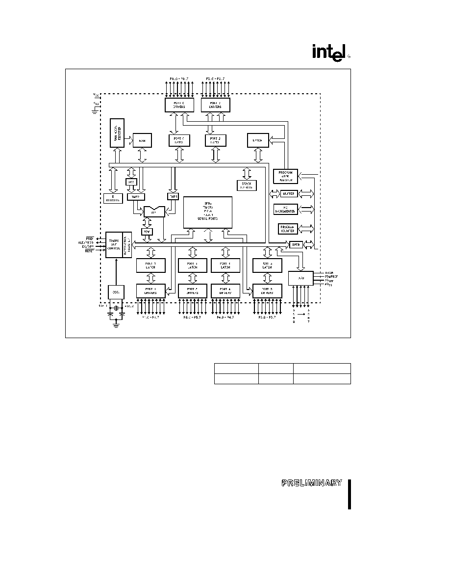
The Intel 8XC51GB is a single-chip control oriented microcontroller which is fabricated on Intel's CHMOS III-E
technology The 8XC51GB is an enhanced version of the 8XC51FA and uses the same powerful instruction
set and architecture as existing MCS 51 microcontroller products Added features make it an even more
powerful microcontroller for applications that require On-Chip A D Pulse Width Modulation High Speed I O
up down counting capabilities and memory protection features It also has a more versatile serial channel that
facilitates multi-processor communications
8XC51GB
272337 ≠ 1
Figure 1 8XC51GB Block Diagram
PROCESS INFORMATION
This device is manufactured on P629 0 a CHMOS
III-E process Additional process and reliability infor-
mation is available in Intel's Components Quality
and Reliability Handbook Order No 210997
PACKAGES
Part
Prefix
Package Type
8XC51GB
N
68-Pin PLCC
2
8XC51GB
PARALLEL I O PORTS
The 8XC51GB contains six 8-bit parallel I O ports
All six ports are bidirectional and consist of a latch
an output driver and an input buffer Many of the
port pins have multiplexed I O and control functions
Port Pins as Outputs
Port 0 has open drain outputs when it is not serving
as the external data bus The internal pullup is active
only when the pin is outputting a logic 1 during exter-
nal memory access An external pullup resistor is
required on Port 0 when it is serving as an output
port
Ports 1 2 3 4 and 5 have quasi-bidirectional out-
puts A strong pullup provides a fast rise time when
the pin is set to a logic 1 This pullup turns on for two
oscillator periods to drive the pin high and then turns
off The pin is held high by a weak pullup
Writing the P0 P1 P2 P3 P4 or P5 Special Function
Register sets the corresponding port pins All six
port registers are bit addressable
Port Pins as Inputs
The pins of all six ports are configured as inputs by
writing a logic 1 to them Since Port 0 is an open
drain port it provides a very high input impedance
Since pins of Port 1 2 3 4 and 5 have weak pullups
(which are always on) they source a small current
when driven low externally All ports except Port 0
have Schmitt trigger inputs
Port States During Reset
Ports 0 and 3 reset asynchronously to a one and
Ports 1 2 4 and 5 reset to a zero asynchronously
PIN DESCRIPTIONS
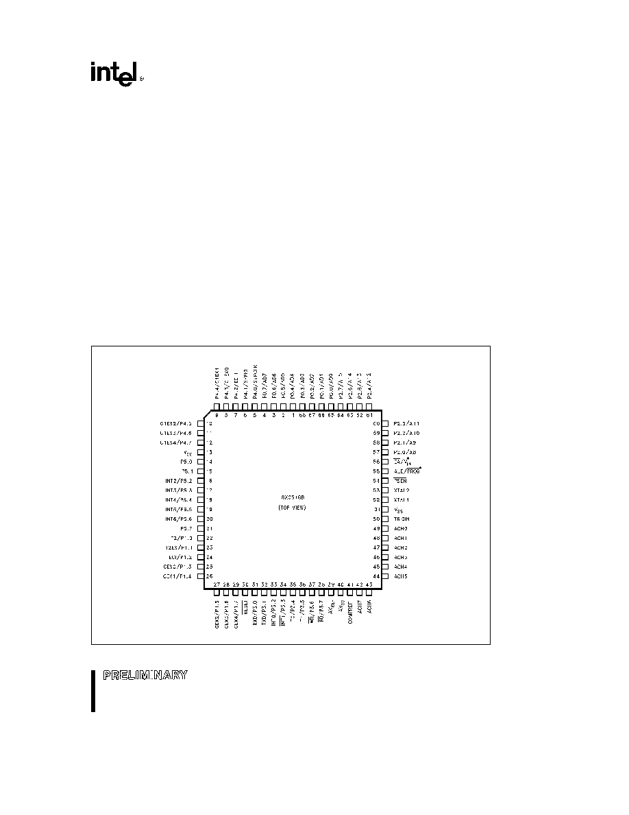
The 8XC51GB will be packaged in the 68-lead PLCC
package Its pin assignment is shown in Figure 2
V
CC
Supply Voltage
V
SS
Circuit Ground
Diagram is for Pin Reference Only Package Size is Not to Scale
272337 ≠ 2
OTP only
Figure 2 Pin Connections
3
8XC51GB
ALTERNATE PORT FUNCTIONS
Ports 0 1 2 3 4 and 5 have alternate functions as well as their I O function as described below
Port Pin
Alternate Function
P0 0 ADO ≠ P0 7 AD7
Multiplexed Address Data for External Memory
P1 0 T2
Timer 2 External Clock Input Clock-Out
P1 1 T2EX
Timer 2 Reload Capture Direction Control
P1 2 ECI
PCA External Clock Input
P1 3 CEXO ≠ P1 7 CEX4
PCA Capture Input Compare PWM Output
P2 0 A8 ≠ P2 7 A15
High Byte of Address for External Memory
P3 0 RXD
Serial Port Input
P3 1 TXD
Serial Port Output
P3 2 INT0
External Interrupt 0
P3 3 INT1
External Interrupt 1
P3 4 T0
Timer 0 External Clock Input
P3 5 T1
Timer 1 External Clock Input
P3 6 WR
Write Strobe for External Memory
P3 7 RD
Read Strobe for External Memory
P4 0 SEPCLK
Clock Source for Serial Expansion Port
P4 1 SEPDAT
Data I O for the Serial Expansion Port
P4 2 ECI1
PCA1 External Clock Input
P4 3 C1EX0 ≠ P4 7 C1EX4
PCA1 Capture Input Compare PWM Output
P5 2 INT2 ≠ P5 6 INT6
External Interrupt INT2 ≠ INT6
RST
Reset input A low on this pin for two machine
cycles while the oscillator is running resets the de-
vice The port pins will be driven to their reset condi-
tion when a voltage below V
IL
max voltage is ap-
plied whether the oscillator is running or not An
internal pullup resistor permits a power-on reset with
only a capacitor connected to V
SS
ALE PROG
Address Latch Enable output pulse for
latching the low byte of the address during accesses
to external memory This pin (ALE PROG) is also
the program pulse input during programming of the
87C51GB
In normal operation ALE is emitted at a constant
rate of
the oscillator frequency and may be used
for external timing or clocking purposes Note how-
ever that one ALE pulse is skipped during each ac-
cess to external Data Memory
If desired ALE operation can be disabled by setting
bit 0 of SFR location 8EH With this bit set the pin is
weakly pulled high However the ALE disable fea-
ture will be suspended during a MOVX or MOVC in-
struction idle mode power down mode and ICE
mode The ALE disable feature will be terminated by
reset When the ALE disable feature is suspended or
terminated the ALE pin will no longer be pulled up
weakly Setting the ALE-disable bit has no affect if
the microcontroller is in external execution mode
Throughout the remainder of this data sheet ALE
will refer to the signal coming out of the ALE PROG
pin and the pin will be referred to as the ALE PROG
pin
PSEN
Program Store Enable is the read strobe to
external Program Memory
When the 8XC51GB is executing code from external
Program Memory PSEN is activated twice each ma-
chine cycle except that two PSEN activations are
skipped during each access to external Data Memo-
ry
EA V
PP
External Access enable
EA must be
strapped to V
SS
in order to enable the device to
fetch code from external Program Memory locations
0000H to 1FFFH Note however that if either of the
Program Lock bits are programmed EA will be inter-
nally latched on reset
EA should be strapped to V
CC
for internal program
executions
4
8XC51GB
This pin also receives the 12 75V programming sup-
ply voltage (V
PP
) during programming (OTP only)
XTAL1
Input to the inverting oscillator amplifier
XTAL2
Output from the inverting oscillator amplifi-
er
A D CONVERTER
The 8XC51GB A D converter has a resolution of 8
bits and an accuracy of
g
1 LSB (
g
2 LSB for chan-
nels 0 and 1) The conversion time for a single chan-
nel is 20 ms at a clock frequency of 16 MHz with the
sample and hold function included Independent
supply voltages are provided for the A D Also the
A D operates both in Normal Mode or in Idle Mode
The A D has 8 analog input pins ACH0 (A D CHan-
nel 0)
ACH7 1 reference input pin COMPREF
(COMParison REFerence) 1 control input pin TRI-
GIN (TRIGger IN) and 2 power pins AVREF (Volt-
age
REFerence)
and
analog
ground
(ANalog
GrouND) In addition the A D has 8 conversion re-
sult registers ADRES0 (A D result for channel 0)
ADRES7 1 comparison result register ACMP (Ana-
log Comparison) and 1 control register ACON (A D
Control)
The control bit ACE (A D Conversion Enable) in
ACON controls whether the A D is in operation or
not ACE e 0 idles the A D ACE e 1 enables A D
conversion The control bit AIM (A D Input mode) in
ACON controls the mode of channel selection AIM
e
0 is the Scan Mode and AIM e 1 is the Select
Mode The result registers ADRES4
ADRES7 al-
ways contain the result of a conversion from the cor-
responding channels ACH4
CH7 However the
result registers ADRES0
ADRES3 depend on the
mode selected In the scan mode ADRES0
AD-
RES3 contain the values from ACH0
ACH3 In
the Select Mode one of the four channels ACH0
ACH3 is converted four times and the four values
are stored sequentially in locations ADRES0
AD-
RES3 Its channel is selected by bits ACS1 and
ACS0 (A D Channel Select 1 and 0) in ACON
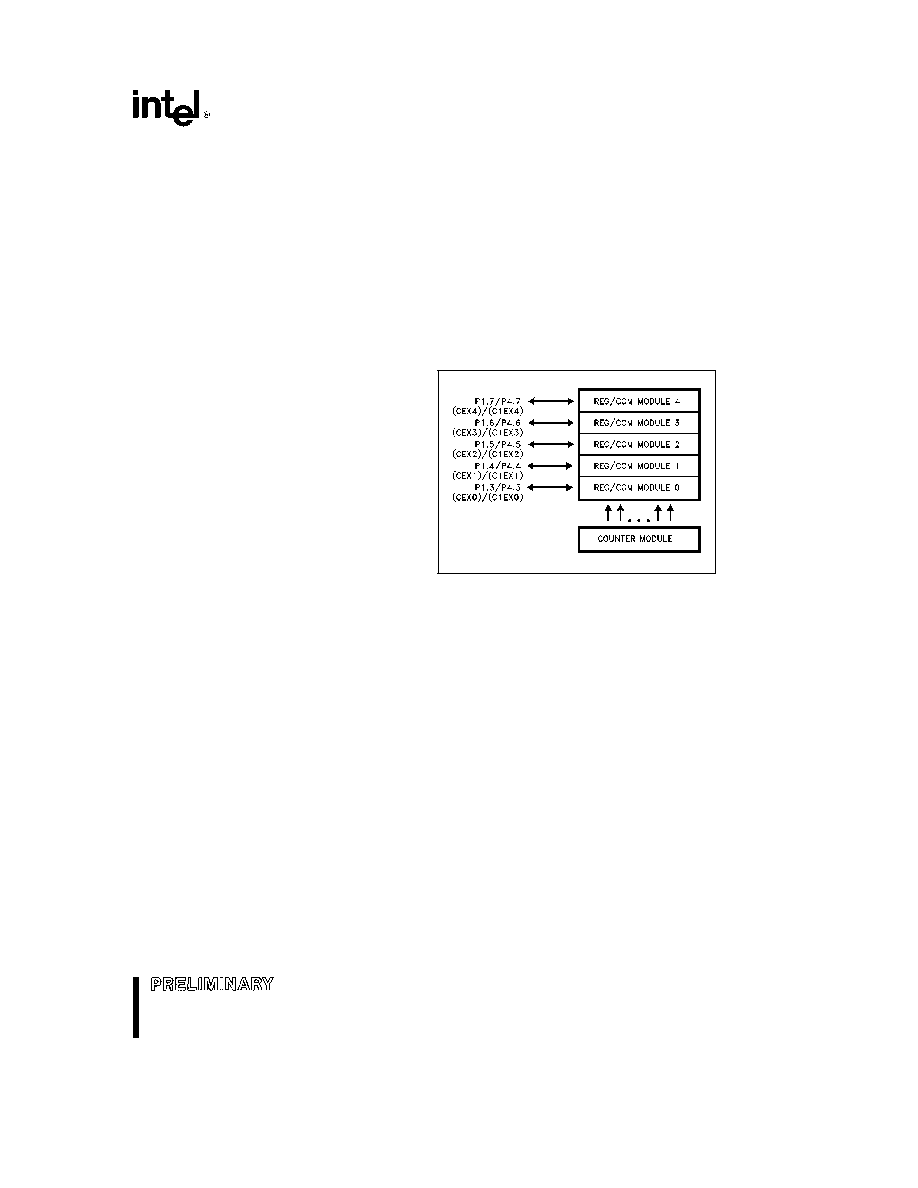
PROGRAMMABLE COUNTER ARRAYS
The Programmable Counter Arrays (PCA ≠ PCA1) are
each made up of a Counter Module and five Regis-
ter Comparator Modules as shown below
The
16-bit output of the counter module is available to all
five Register Comparator Modules providing one
common timing reference Each Register Compara-
tor Module is associated with a pin of Port 1 or Port 4
and is capable of performing input capture output
compare and pulse width modulation functions The
PCAs are exactly the same in function except for the
addition of clock input sources on PCA1
The PCA Counter and five Register Comparator
Modules each have a status bit in the CCON
C1CON Special Function Registers
These six
status bits are set according to the selected modes
of operation described below The CCON C1CON
Register provides a convenient means to determine
which of the six PCA PCA1 interrupts has occurred
The EC Bit in the IE (Interrupt Enable) Special Func-
tion Register is a global interrupt enable for the PCA
272337 ≠ 3
Figure 3 Programmable Counter Arrays
OSCILLATOR CHARACTERISTICS
XTAL1 and XTAL2 are the input and output respec-
tively of an inverting amplifier which can be config-
ured for use as an on-chip oscillator as shown in
Figure 4 Either a quartz crystal or ceramic resonator
may be used More detailed information concerning
the use of the on-chip oscillator is available in Appli-
cation Note AP-155 ``Oscillators for Microcontrol-
lers '' Order No 230659
To drive the device from an external clock source
XTAL should be driven while XTAL2 floats as
shown in Figure 5 There are no requirements on the
duty cycle of the external clock signal since the in-
put to the internal clocking circuitry is through a di-
vide-by-two flip-flop but minimum and maximum
high and low times specified on the data sheet must
be observed
5