 | –≠–ª–µ–∫—Ç—Ä–æ–Ω–Ω—ã–π –∫–æ–º–ø–æ–Ω–µ–Ω—Ç: 83L51FB | –°–∫–∞—á–∞—Ç—å:  PDF PDF  ZIP ZIP |
Other brands and names are the property of their respective owners
Information in this document is provided in connection with Intel products Intel assumes no liability whatsoever including infringement of any patent or
copyright for sale and use of Intel products except as provided in Intel's Terms and Conditions of Sale for such products Intel retains the right to make
changes to these specifications at any time without notice Microcomputer Products may have minor variations to this specification known as errata
November 1994
COPYRIGHT
INTEL CORPORATION 1995
Order Number 272356-003
8XL51FA FB FC
LOW VOLTAGE
CHMOS SINGLE-CHIP 8-BIT MICROCONTROLLERS
Commercial Express
87L51FA 83L51FA 80L51FA 87L51FB 83L51FB 87L51FC 83L51FC
Y
High Performance CHMOS OTP ROM
ROM CPU
Y
Low Voltage Operation
Y
20 MHz Commercial 16 MHz Express
Operation
Y
Three 16-Bit Timer Counters
Y
Programmable Counter Array with
High Speed Output
Compare Capture
Pulse Width Modulator
Watchdog Timer Capabilities
Y
Up Down Timer Counter
Y
Three Level Program Lock System
Y
8K 16K 32K On-Chip Program Memory
Y
256 Bytes of On-Chip Data RAM
Y
Improved Quick Pulse Programming
Algorithm
Y
Boolean Processor
Y
32 Programmable I O Lines
Y
7 Interrupt Sources
Y
Four Level Interrupt Priority
Y
Programmable Serial Channel with
Framing Error Detection
Automatic Address Recognition
Y
64K External Program Memory Space
Y
64K External Data Memory Space
Y
MCS
51 Microcontroller Compatible
Instruction Set
Y
Power Saving Idle and Power Down
Modes
Y
ONCE (On-Circuit Emulation) Mode
Y
Extended Temperature Range
(
b
40 C to
a
85 C)
MEMORY ORGANIZATION
Device
ROM
OTP ROM
Version
ROMLESS
Version
ROM
Bytes
RAM
OTP ROM
Bytes
83L51FA
87L51FA
80L51FA
8K
256
83L51FB
87L51FB
80L51FA
16K
256
83L51FC
87L51FC
80L51FA
32K
256
These devices can address up to 64 Kbytes of external program data memory
The Intel 8XL51FA 8XL51FB 8XL51FC is a single-chip control oriented microcontroller which is fabricated on
Intel's reliable CHMOS III-E technology Being a member of the MCS
51 microcontroller family the
8XL51FA 8XL51FB 8XL51FC uses the same powerful instruction set has the same architecture and is pin-
for-pin compatible with the existing MCS 51 microcontroller products
The 8XL51FX is a 3V version of current 8XC51FX and will operate from 2 7V to 3 6V at a frequency range of
3 5 MHz to 16 MHz (Express) 20 MHz (Commercial)
For the remainder of this document the 8XL51FA 8XL51FB 8XL51FC will be referred to as the 8XL51FX
unless information applies to a specific device

8XL51FA FB FC
Standard
b
1
b
20
80L51FA
X
X
X
83L51FA
X
X
X
87L51FA
X
X
X
83L51FB
X
X
X
87L51FB
X
X
X
83L51FC
X
X
X
87L51FC
X
X
X
NOTE
Standard
3 5 MHz to 12 MHz 2 7V to 3 6V
b
1
3 5 MHz to 16 MHz 2 7V to 3 6V
b
20
3 5 MHz to 20 MHz 2 7V to 3 6V
Only available for commercial standard temperature
range not available at express temperature range
272356 ≠ 1
Figure 1 8XL51FX Block Diagram
2

8XL51FA FB FC
PROCESS INFORMATION
The 8XL51FA 8XL51FB 8XL51FC is manufactured
on P629 5 a CHMOS III-E process Additional pro-
cess and reliability information is available in Intel's
Components Quality and Reliability Handbook
Or-
der Number 210997
PACKAGES
Part
Prefix
Package Type
8XL51FX
N
44-Pin PLCC
(OTP)
S
44-Pin QFP
(OTP)
272356 ≠ 2
PLCC
272356 ≠ 3
QFP
Figure 2 Pin Connections
3

8XL51FA FB FC
PIN DESCRIPTIONS
V
CC
Supply voltage
V
SS
Circuit ground
Port 0 Port 0 is an 8-bit open drain bidirectional I O
port As an output port each pin can sink several
inputs Port 0 pins that have 1's written to them float
and in that state can be used as high-impedance
inputs
Port 0 is also the multiplexed low-order address and
data bus during accesses to external Program and
Data Memory In this application it uses strong inter-
nal pullups when emitting 1's and can source and
sink several inputs
Port 0 also receives the code bytes during OTP
ROM programming and outputs the code bytes dur-
ing program verification External pullup resistors are
required during program verification
Port 1 Port 1 is an 8-bit bidirectional I O port with
internal pullups The Port 1 output buffers can drive
several inputs Port 1 pins that have 1's written to
them are pulled high by the internal pullups and in
that state can be used as inputs As inputs Port 1
pins that are externally pulled low will source current
(I
IL
on the data sheet) because of the internal pull-
ups
In addition Port 1 serves the functions of the follow-
ing special features of the 8XL51FX
Port Pin
Alternate Function
P1 0
T2 (External Count Input to Timer
Counter 2) Clock Out
P1 1
T2EX (Timer Counter 2 Capture
Reload Trigger and Direction Control)
P1 2
ECI (External Count Input to the PCA)
P1 3
CEX0 (External I O for Compare
Capture Module 0)
P1 4
CEX1 (External I O for Compare
Capture Module 1)
P1 5
CEX2 (External I O for Compare
Capture Module 2)
P1 6
CEX3 (External I O for Compare
Capture Module 3)
P1 7
CEX4 (External I O for Compare
Capture Module 4)
Port 1 receives the low-order address bytes during
OTP ROM programming and verifying
Port 2 Port 2 is an 8-bit bidirectional I O port with
internal pullups The Port 2 output buffers can drive
several inputs Port 2 pins that have 1's written to
them are pulled high by the internal pullups and in
that state can be used as inputs As inputs Port 2
pins that are externally pulled low will source current
(I
IL
on the data sheet) because of the internal pull-
ups
Port 2 emits the high-order address byte during
fetches from external Program Memory and during
accesses to external Data Memory that use 16-bit
addresses (MOVX
DPTR) In this application it
uses strong internal pullups when emitting 1's Dur-
ing accesses to external Data Memory that use 8-bit
addresses (MOVX
Ri) Port 2 emits the contents of
the P2 Special Function Register
Some Port 2 pins receive the high-order address bits
during OTP ROM programming and program verifi-
cation
Port 3 Port 3 is an 8-bit bidirectional I O port with
internal pullups The Port 3 output buffers can drive
several inputs Port 3 pins that have 1's written to
them are pulled high by the internal pullups and in
that state can be used as inputs As inputs Port 3
pins that are externally pulled low will source current
(I
IL
on the data sheet) because of the pullups
Port 3 also serves the functions of various special
features of the MCS 51 microcontroller family as
listed below
Port Pin
Alternate Function
P3 0
RXD (serial input port)
P3 1
TXD (serial output port)
P3 2
INT0 (external interrupt 0)
P3 3
INT1 (external interrupt 1)
P3 4
T0 (Timer 0 external input)
P3 5
T1 (Timer 1 external input)
P3 6
WR (external data memory write strobe)
P3 7
RD (external data memory read strobe)
RST Reset input A high on this pin for two machine
cycles while the oscillator is running resets the de-
vice The port pins will be driven to their reset condi-
tion when a minimum V
IH2
voltage is applied wheth-
er the oscillator is running or not An internal pull-
down resistor permits a power-on reset with only a
capacitor connected to V
CC
4
8XL51FA FB FC
ALE Address Latch Enable output pulse for latching
the low byte of the address during accesses to ex-
ternal memory This pin (ALE PROG) is also the
program pulse input during OTP ROM programming
for the 87L51FX
In normal operation ALE is emitted at a constant
rate of
the oscillator frequency and may be used
for external timing or clocking purposes Note how-
ever that one ALE pulse is skipped during each ac-
cess to external Data Memory
If desired ALE operation can be disabled by setting
bit 0 of SFR location 8EH With this bit set the pin is
weakly pulled high However the ALE disable fea-
ture will be suspended during a MOVX or MOVC in-
struction idle mode power down mode and ICE
mode The ALE disable feature will be terminated by
reset When the ALE disable feature is suspended or
terminated the ALE pin will no longer be pulled up
weakly Setting the ALE-disable bit has no affect if
the microcontroller is in external execution mode
Throughout the remainder of this data sheet ALE
will refer to the signal coming out of the ALE PROG
pin and the pin will be referred to as the ALE PROG
pin
PSEN Program Store Enable is the read strobe to
external Program Memory
When the 8XL51FX is executing code from external
Program Memory PSEN is activated twice each ma-
chine cycle except that two PSEN activations are
skipped during each access to external Data Memo-
ry
EA V
PP
External Access enable
EA must be
strapped to VSS in order to enable the device to
fetch code from external Program Memory locations
0000H to 0FFFH Note however that if either of the
Program Lock bits are programmed EA will be inter-
nally latched on reset
EA must be strapped to V
CC
for internal program
executions
This pin also receives the programming supply volt-
age (V
PP
) during OTP ROM programming
XTAL1 Input to the inverting oscillator amplifier
XTAL2 Output from the inverting oscillator amplifier
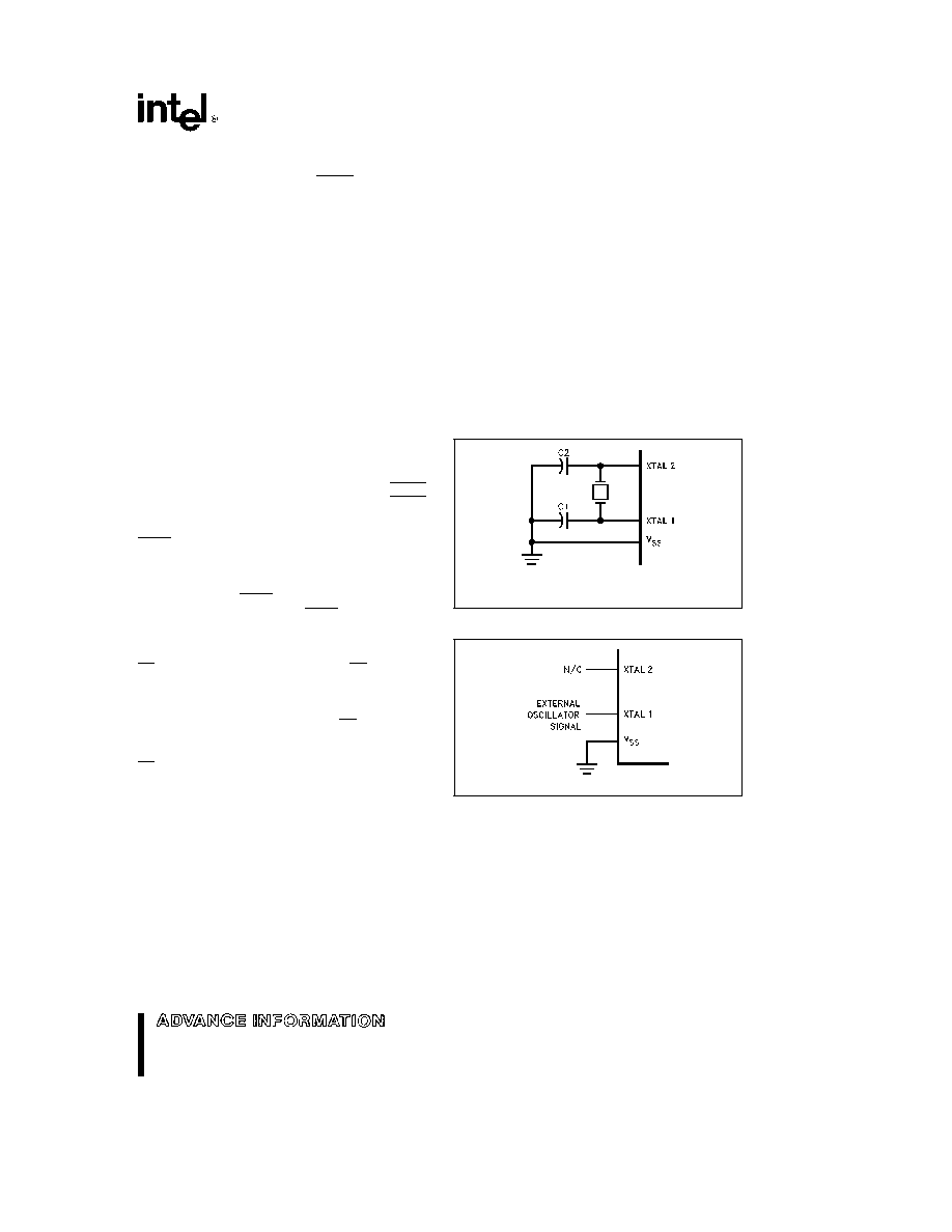
OSCILLATOR CHARACTERISTICS
XTAL1 and XTAL2 are the input and output respec-
tively of a inverting amplifier which can be config-
ured for use as an on-chip oscillator as shown in
Figure 3 Either a quartz crystal or ceramic resonator
may be used More detailed information concerning
the use of the on-chip oscillator is available in Appli-
cation Note AP-155 ``Oscillators for Microcontrol-
lers ''
To drive the device from an external clock source
XTAL1 should be driven while XTAL2 floats as
shown in Figure 4 There are no requirements on the
duty cycle of the external clock signal since the in-
put to the internal clocking circuitry is through a di-
vide-by-two flip-flop but minimum and maximum
high and low times specified on the data sheet must
be observed
An external oscillator may encounter as much as a
100 pF load at XTAL1 when it starts up This is due
to interaction between the amplifier and its feedback
capacitance Once the external signal meets the V
IL
and V
IH
specifications the capacitance will not ex-
ceed 20 pF
272356 ≠ 4
C1 C2 e 30 pF
g
10 pF for Crystals
For Ceramic Resonators contact resonator manufacturer
Figure 3 Oscillator Connections
272356 ≠ 5
Figure 4 External Clock Drive Configuration
IDLE MODE
The user's software can invoke the Idle Mode When
the microcontroller is in this mode power consump-
tion is reduced The Special Function Registers and
the onboard RAM retain their values during Idle but
the processor stops executing instructions
Idle
Mode will be exited if the chip is reset or if an en-
abled interrupt occurs The PCA timer counter can
optionally be left running or paused during Idle
Mode
5