 | –≠–ª–µ–∫—Ç—Ä–æ–Ω–Ω—ã–π –∫–æ–º–ø–æ–Ω–µ–Ω—Ç: 8742 | –°–∫–∞—á–∞—Ç—å:  PDF PDF  ZIP ZIP |
Document Outline
- 8742 UNIVERSAL PERIPHERAL INTERFACE 8-BIT SLAVE MICROCONTROLLER
- Pin Description
- UPI-42 FEATURES
- APPLICATIONS
- PROGRAMMING, VERIFYING, AND ERASING THE 8742 EPROM
- ProgrammingVerification
- 8742ErasureCharacteristics
- ABSOLUTE MAXIMUM RATINGS*
- D.C. CHARACTERISTICS
- D.C. CHARACTERISTICSÖPROGRAMMING
- A.C. CHARACTERISTICS
- DBBREAD
- DBBWRITE
- PROGRAMMING
- A.C. CHARACTERISTICS (DMA)
- A.C. CHARACTERISTICS (PORT 2)
- A.C.TESTINGINPUT/OUTPUTWAVEFORM
- A.C.TESTINGLOADCIRCUIT
- CRYSTAL OSCILLATOR MODE
- DRIVING FROM EXTERNAL SOURCE
- LCOSCILLATORMODE
- WAVEFORMS
- READ OPERATIONÖDATA BUS BUFFER REGISTER
- WRITE OPERATIONÖDATA BUS BUFFER REGISTER
- CLOCK TIMING
- COMBINATION PROGRAM/VERIFY MODE
- VERIFY MODE
- DMA
- PORT 2
- PORT TIMING DURING EXTERNAL ACCESS (EA)
November 1991
Order Number 290256-001
8742
UNIVERSAL PERIPHERAL INTERFACE
8-BIT SLAVE MICROCONTROLLER
Y
8742 12 MHz
Y
Pin Software and Architecturally
Compatible with 8741A
Y
8-Bit CPU plus ROM RAM I O Timer
and Clock in a Single Package
Y
2048 x 8 EPROM 128 x 8 RAM 8-Bit
Timer Counter 18 Programmable I O
Pins
Y
One 8-Bit Status and Two Data
Registers for Asynchronous Slave-to-
Master Interface
Y
DMA Interrupt or Polled Operation
Supported
Y
Fully Compatible with all Intel and Most
Other Microprocessor Families
Y
Expandable I O
Y
RAM Power-Down Capability
Y
Over 90 Instructions 70% Single Byte
Y
Available in EXPRESS
Standard Temperature Range
The Intel 8742 is a general-purpose Universal Peripheral Interface that allows designers to grow their own
customized solution for peripheral device control It contains a low-cost microcomputer with 2K of program
memory 128 bytes of data memory 8-bit timer counter and clock generator in a single 40-pin package
Interface registers are included to enable the UPI device to function as a peripheral controller in the MCS -48
MCS-51 MCS-80 MCS-85 8088 8086 and other 8- 16-bit systems
The 8742 is software pin and architecturally compatible with the 8741A The 8742 doubles the on-chip
memory space to allow for additional features and performance to be incorporated in upgraded 8741A de-
signs For new designs the additional memory and performance of the 8742 extends the UPI concept to more
complex motor control tasks 80-column printers and process control applications as examples
290256 ≠ 2
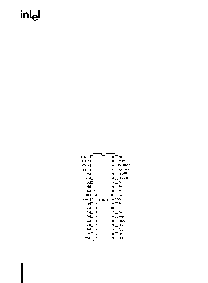
Figure 1 Pin Configuration
1
8742
290256 ≠ 1
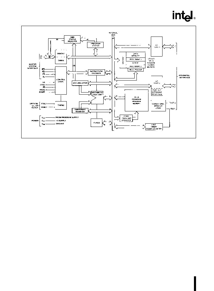
Figure 2 Block Diagram
2
2
8742
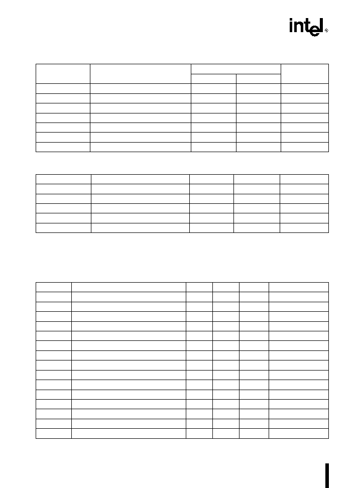
Table 1 Pin Description
DIP
Symbol
Pin
Type
Name and Function
No
TEST 0
1
I
TEST INPUTS
Input pins which can be directly tested using conditional branch
instructions
TEST 1
39
FREQUENCY REFERENCE
TEST 1 (T
1
) also functions as the event timer input (under
software control) TEST 0 (T
0
) is used during PROM programming and EPROM
verification
XTAL 1
2
I
INPUTS
Inputs for a crystal LC or an external timing signal to determine the internal
oscillator frequency
XTAL 2
3
RESET
4
I
RESET
Input used to reset status flip-flops and to set the program counter to zero
RESET is also used during EPROM programming and verification
SS
5
I
SINGLE STEP
Single step input used in conjunction with the SYNC output to step the
program through each instruction (EPROM) This should be tied to
a
5V when not used
CS
6
I
CHIP SELECT
Chip select input used to select one UPI microcomputer out of several
connected to a common data bus
EA
7
I
EXTERNAL ACCESS
External access input which allows emulation testing and EPROM
verification This pin should be tied low if unused
RD
8
I
READ
I O read input which enables the master CPU to read data and status words from
the OUTPUT DATA BUS BUFFER or status register
A
0
9
I
COMMAND DATA SELECT
Address Input used by the master processor to indicate
whether byte transfer is data (A
0
e
0 F1 is reset) or command (A
0
e
1 F1 is set) A
0
e
0
during program and verify operations
WR
10
I
WRITE
I O write input which enables the master CPU to write data and command words
to the UPI INPUT DATA BUS BUFFER
SYNC
11
O
OUTPUT CLOCK
Output signal which occurs once per UPI instruction cycle SYNC can
be used as a strobe for external circuitry it is also used to synchronize single step
operation
(BUS)
D
0
≠ D
7
12 ≠ 19
I O
DATA BUS
Three-state bidirectional DATA BUS BUFFER lines used to interface the UPI
microcomputer to an 8-bit master system data bus
P
10
≠ P
17
27 ≠ 34
I O
PORT 1
8-bit PORT 1 quasi-bidirectional I O lines
P
20
≠ P
27
21 ≠ 24
I O
PORT 2
8-bit PORT 2 quasi-bidirectional I O lines The lower 4 bits (P
20
≠ P
23
) interface
directly to the 8243 I O expander device and contain address and data information during
35 ≠ 38
PORT 4 ≠ 7 access The upper 4 bits (P
24
≠ P
27
) can be programmed to provide interrupt
Request and DMA Handshake capability Software control can configure P
24
as Output
Buffer Full (OBF) interrupt P
25
as Input Buffer Full (IBF) interrupt P
26
as DMA Request
(DRQ) and P
27
as DMA ACKnowledge (DACK)
PROG
25
I O
PROGRAM
Multifunction pin used as the program pulse input during PROM programming
During I O expander access the PROG pin acts as an address data strobe to the 8243
This pin should be tied high if unused
V
CC
40
POWER
a
5V main power supply pin
V
DD
26
POWER
a
5V during normal operation
a
21V during programming operation Low power
standby supply pin
V
SS
20
GROUND
Circuit ground potential
3
3

8742
UPI-42 FEATURES
1
Two Data Bus Buffers one for input and one for
output This allows a much cleaner Master Slave
protocol
290256 ≠ 3
2
8 Bits of Status
ST
7
ST
6
ST
5
ST
4
F
1
F
0
IBF OBF
D
7
D
6
D
5
D
4
D
3
D
2
D
1
D
0
ST
4
≠ ST
7
are user definable status bits These
bits are defined by the ``MOV STS A'' single byte
single cycle instruction Bits 4 ≠ 7 of the acccumu-
lator are moved to bits 4 ≠ 7 of the status register
Bits 0 ≠ 3 of the status register are not affected
MOV STS A
Op Code 90H
1
0
0
1
0
0
0
0
D
7
D
0
3
RD and WR are edge triggered IBF OBF F
1
and
INT change internally after the trailing edge of RD
or WR
290256 ≠ 4
During the time that the host CPU is reading the
status register the 8742 is prevented from updat-
ing this register or is ``locked out''
4
P
24
and P
25
are port pins or Buffer Flag pins
which can be used to interrupt a master proces-
sor These pins default to port pins on Reset
If the ``EN FLAGS'' instruction has been execut-
ed P
24
becomes the OBF (Output Buffer Full) pin
A ``1'' written to P
24
enables the OBF pin (the pin
outputs the OBF Status Bit) A ``0'' written to P
24
disables the OBF pin (the pin remains low) This
pin can be used to indicate that valid data is avail-
able from the UPI-41A (in Output Data Bus Buff-
er)
If ``EN FLAGS'' has been executed P
25
becomes
the IBF (Input Buffer Full) pin A ``1'' written to P
25
enables the IBF pin (the pin outputs the inverse of
the IBF Status Bit A ``0'' written to P
25
disables
the IBF pin (the pin remains low) This pin can be
used to indicate that the UPI is ready for data
290256 ≠ 5
Data Bus Buffer Interrupt Capability
EN FLAGS
Op Code 0F5H
1
1
1
1
0
1
0
1
D
7
D
0
5
P
26
and P
27
are port pins or DMA handshake pins
for use with a DMA controller These pins default
to port pins on Reset
If the ``EN DMA'' instruction has been executed
P
26
becomes the DRQ (DMA Request) pin A ``1''
written to P
26
causes a DMA request (DRQ is acti-
vated)
DRQ
is
deactivated
by
DACK
#
RD
DACK
#
WR or execution of the ``EN DMA'' in-
struction
If ``EN DMA'' has been executed P
27
becomes
the DACK (DMA Acknowledge) pin This pin acts
as a chip select input for the Data Bus Buffer reg-
isters during DMA transfers
290256 ≠ 6
DMA Handshake Capability
EN DMA
Op Code 0E5H
1
1
1
0
0
1
0
1
D
7
D
0
6
The RESET input on the 8742 includes a 2-stage
synchronizer to support reliable reset operation
for 12 MHz operation
7
When EA is enabled on the 8742 the program
counter is placed on Port 1 and the lower three
bits of Port 2 (MSB e P
22
LSB e P
10
) On the
8742 this information is multiplexed with PORT
DATA (see port timing diagrams at end of this
data sheet)
4
4

8742
APPLICATIONS
290256 ≠ 7
Figure 3 8088-8742 Interface
290256 ≠ 9
Figure 5 8742-8243 Keyboard Scanner
290256 ≠ 8
Figure 4 8048H-8742 Interface
290256 ≠ 10
Figure 6 8742 80-Column
Matrix Printer Interface
5
5

8742
PROGRAMMING VERIFYING AND
ERASING THE 8742 EPROM
Programming Verification
In brief the programming process consists of acti-
vating the program mode applying an address
latching the address applying data and applying a
programming pulse Each word is programmed com-
pletely before moving on to the next and is followed
by a verification step The following is a list of the
pins used for programming and a description of their
functions
Pin
Function
XTAL 1
Clock-Input
Reset
Initialization and Address Latching
Test 0
Selection of Program or Verify Mode
EA
Activation of Program Verify Modes
BUS
Address and Data Input
Data Output During Verify
P
20≠12
Address Input
V
DD
Programming Power Supply
PROG
Program Pulse Input
WARNING
An attempt to program a missocketed 8742 will result in severe dam-
age to the part An indication of a properly socketed part is the ap-
pearance of the SYNC clock output The lack of this clock may be
used to disable the programmer
The Program Verify sequence is
1 A
0
e
0V CS e 5V EA e 5V RESET e 0V
TESTO e 5V V
DD
e
5V clock applied or inter-
nal oscillator operating BUS floating PROG e
5V
2 Insert 8742 in programming socket
3 TEST 0 e 0V (select program mode)
4 EA e 18V (active program mode)
5 Address applied to BUS and P
20≠22
6 RESET e 5V (latch address)
7 Data applied to BUS
8 V
DD
e
21V (programming power)
9 PROG e V
CC
followed by one 50 ms pulse to
18V
10 V
DD
e
5V
11 TEST 0 e 5V (verify mode)
12 Read and verify data on BUS
13 TEST 0 e 0V
14 RESET e 0V and repeat from step 5
15 Programmer should be at conditions of step 1
when 8742 is removed from socket
8742 Erasure Characteristics
The erasure characteristics of the 8742 are such
that erasure begins to occur when exposed to light
with wavelengths shorter than approximately 4000
Angstroms ( ) It should be noted that sunlight and
certain types of fluorescent lamps have wavelengths
in the 3000-4000
range Data shows that constant
exposure to room level fluorescent lighting could
erase the typical 8742 in approximately 3 years
while it would take approximately one week to cause
erasure when exposed to direct sunlight If the 8742
is to be exposed to these types of lighting conditions
for extended periods of time opaque labels are
available from Intel which should be placed over the
8742 window to prevent unintentional erasure
The recommended erasure procedure for the 8742
is exposure to shortwave ultraviolet light which has a
wavelength of 2537
The integrated dose (i e UV
intensity
c
exposure time) for erasure should be a
minimum of 15 w-sec cm
2
The erasure time with
this dosage is approximately 15 to 20 minutes using
an ultraviolet lamp with a 12 000 mW cm
2
power rat-
ing The 8742 should be placed within one inch of
the lamp tubes during erasure Some lamps have a
filter on their tubes which should be removed before
erasure
6
6
8742
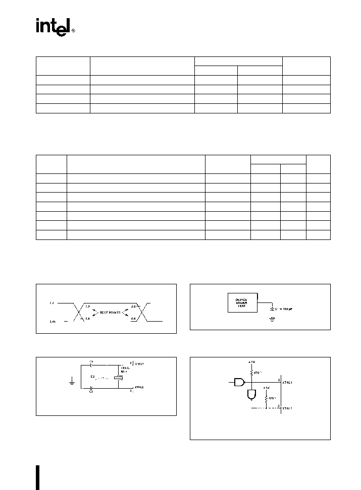
ABSOLUTE MAXIMUM RATINGS
Ambient Temperature Under Bias
0 C to 70 C
Storage Temperature
b
65 C to a150 C
Voltage on Any Pin With Respect
to Ground
b
0 5 to a7V
Power Dissipation
1 5W
NOTICE This is a production data sheet The specifi-
cations are subject to change without notice
WARNING Stressing the device beyond the ``Absolute
Maximum Ratings'' may cause permanent damage
These are stress ratings only Operation beyond the
``Operating Conditions'' is not recommended and ex-
tended exposure beyond the ``Operating Conditions''
may affect device reliability
D C CHARACTERISTICS
T
A
e
0 to a70 C V
CC
e
V
DD
e a
5V
g
10%
Symbol
Parameter
8742
Units
Test
Min
Max
Conditions
V
IL
Input Low Voltage (Except XTAL1 XTAL2 RESET)
b
0 5
0 8
V
V
IL1
Input Low Voltage (XTAL1 XTAL2 RESET)
b
0 5
0 6
V
V
IH
Input High Voltage (Except XTAL1 XTAL2 RESET)
2 0
V
CC
V
V
IH1
Input High Voltage (XTLA1 XTAL2 RESET)
3 5
V
CC
V
V
OL
Output Low Voltage (D
0
≠ D
7
)
0 45
V
I
OL
e
2 0 mA
V
OL1
Output Low Voltage (P
10
≠ P
17
P
20
≠ P
27
Sync)
0 45
V
I
OL
e
1 6 mA
V
OL2
Output Low Voltage (PROG)
0 45
V
I
OL
e
1 0 mA
V
OH
Output High Voltage (D
0
≠ D
7
)
2 4
V
I
OH
e b
400 mA
V
OH1
Output High Voltage (All Other Outupts)
2 4
I
OH
e b
50 mA
I
IL
Input Leakage Current (T
0
T
1
RD WR CS A
0
EA)
g
10
m
A
V
SS
s
V
IN
s
V
CC
I
OFL
Output Leakage Current (D
0
≠ D
7
High Z State)
g
10
m
A
V
SS
a
0 45
s
V
OUT
s
V
CC
I
LI
Low Input Load Current (P
10
≠ P
17
P
20
≠ P
27
)
0 3
mA
V
IL
e
0 8V
I
LI1
Low Input Load Current (RESET SS)
0 2
mA
V
IL
e
0 8V
I
DD
V
DD
Supply Current
10
mA
Typical e 5 mA
I
CC
a
I
DD
Total Supply Current
125
mA
Typical e 60 mA
I
IH
Input Leakage Current (P
10
≠ P
17
P
20
≠ P
27
)
100
m
A
V
IN
e
V
CC
C
IN
Input Capacitance
10
pF
C
1 0
I O Capacitance
20
pF
D C CHARACTERISTICS
PROGRAMMING
T
A
e
25 C
g
5 C V
CC
e
5V
g
5% V
DD
e
21V
g
0 5V
Symbol
Parameter
Min
Max
Units
Test Conditions
V
DOH
V
DD
Program Voltage High Level
20 5
21 5
V
V
DDL
V
DD
Voltage Low Level
4 75
5 25
V
V
PH
PROG Program Voltage High Level
17 5
18 5
V
V
PL
PROG Voltage Low Level
V
CC
b
0 5
V
CC
V
V
EAH
EA Program or Verify Voltage High Level
17 5
18 5
V
V
EAL
EA Voltage Low Level
5 25
V
I
DD
V
DD
High Voltage Supply Current
30 0
mA
I
PROG
PROG High Voltage Supply Current
1 0
mA
I
EA
EA High Voltage Supply Current
1 0
mA
7
7
8742
A C CHARACTERISTICS
T
A
e
0 C to a70 C V
SS
e
0V V
CC
e
V
DD
e a
5V
g
10%
DBB READ
Symbol
Parameter
8742
Units
Min
Max
t
AR
CS A
0
Setup to RD
v
0
ns
t
RA
CS A
0
Hold after RD
u
0
ns
t
RR
RD Pulse Width
160
ns
t
AD
CS A
0
to Data Out Delay
130
ns
t
RD
RD
v
to Data Out Delay
130
ns
t
DF
RD
u
to Data Float Delay
85
ns
t
CY
Cycle Time
1 25
15
m
s
(1)
DBB WRITE
Symbol
Parameter
Min
Max
Units
t
AW
CS A
0
Setup to WR
v
0
ns
t
WA
CS A
0
Hold after WR
u
0
ns
t
WW
WR Pulse Width
160
ns
t
DW
Data Setup to WR
u
130
ns
t
WD
Data Hold after WR
u
0
ns
NOTE
1 T
CY
e
15 f(XTAL)
A C CHARACTERISTICS
T
A
e
25 C
g
5 C V
CC
e
5V
g
5% V
DD
e a
21V
g
0 5
PROGRAMMING
Symbol
Parameter
Min
Max
Units
Test Conditions
t
AW
Address Setup Time to RESET
u
4t
CY
t
WA
Address Hold Time after RESET
u
4t
CY
t
DW
Data in Setup Time to PROG
u
4t
CY
t
WD
Data in Hold Time after PROG
v
4t
CY
t
PH
RESET Hold Time to Verify
4t
CY
t
VDDW
V
DD
Setup Time to PROG
u
0
1 0
mS
t
VDDH
V
DD
Hold Time after PROG
u
0
1 0
mS
t
PW
Program Pulse Width
50
60
mS
t
TW
Test 0 Setup Time for Program Mode
4t
CY
t
WT
Test 0 Hold Time after Program Mode
4t
CY
t
DO
Test 0 to Data Out Delay
4t
CY
t
WW
RESET Pulse Width to Latch Address
4t
CY
t
r
t
f
V
DD
and PROG Rise and Fall Times
0 5
2 0
m
s
t
CY
CPU Operation Cycle Time
4 0
m
s
t
RE
RESET Setup Time before EA
u
4t
CY
NOTE
If TEST 0 is high t
DO
can be triggered by RESET
u
8
8
8742
A C CHARACTERISTICS
DMA
Symbol
Parameter
8642 8742
Units
Min
Max
t
ACC
DACK to WR or RD
0
ns
t
CAC
RD or WR to DACK
0
ns
t
ACD
DACK to Data Valid
130
ns
t
CRQ
RD or WR to DRQ Cleared
100
ns
(1)
NOTE
1 C
L
e
150 pF
A C CHARACTERISTICS
PORT 2
T
A
e
0 C to a70 C V
CC
e a
5V
g
10%
Symbol
Parameter
f(t
CY
)
8742 8642
(3)
Units
Min
Max
t
CP
Port Control Setup before Falling Edge of PROG
1 15 t
CY
b
28
55
ns
(1)
t
PC
Port Control Hold after Falling Edge of PROG
1 10 t
CY
125
ns
(2)
t
PR
PROG to Time P2 Input Must Be Valid
8 15 t
CY
b
16
650
ns
(1)
t
PF
Input Data Hold Time
0
150
ns
(2)
t
DP
Output Data Setup Time
2 10 t
CY
250
ns
(1)
t
PD
Output Data Hold Time
1 10 t
CY
b
80
45
ns
(2)
t
PP
PROG Pulse Width
6 10 t
CY
750
ns
NOTES
1 C
L
e
80 pF
2 C
L
e
20 pF
3 t
CY
e
1 25 ms
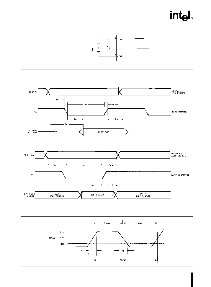
A C TESTING INPUT OUTPUT WAVEFORM
INPUT OUTPUT
290256 ≠ 11
A C TESTING LOAD CIRCUIT
290256 ≠ 12
CRYSTAL OSCILLATOR MODE
290256 ≠ 13
Crystal Series Resistance Should be
k
750 at 12 MHz
k
180X at 3 6 MHz
DRIVING FROM EXTERNAL SOURCE
290256 ≠ 14
Rise and Fall Times Should Not Exceed 20 ns Resis-
tors to V
CC
are Needed to Ensure V
IH
e
3 5V if TTL
Circuitry is Used
9
9
8742
LC OSCILLATOR MODE
f e
1
2
q
0LC
L
C
NOMINAL
45 H 20 pF
5 2 MHz
C e
C a 3Cpp
2
120 H 20 pF
3 2 MHz
Cpp j 5 pF ≠ 10 pF
Pin-to-Pin Capacitance
290256 ≠ 15
Each C Should be Approximately 20 pF including Stray Capacitance
WAVEFORMS
READ OPERATION
DATA BUS BUFFER REGISTER
290256 ≠ 16
WRITE OPERATION
DATA BUS BUFFER REGISTER
290256 ≠ 17
CLOCK TIMING
290256 ≠ 23
10
10
8742
WAVEFORMS
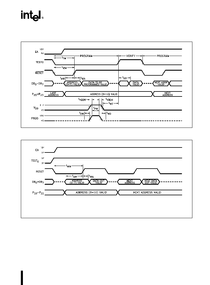
COMBINATION PROGRAM VERIFY MODE
290256 ≠ 18
VERIFY MODE
290256 ≠ 19
NOTES
1 PROG must float if EA is low or EA is low or if TEST
0
e
5V
2 A
0
must be held low (i e
e
0V) during program verify modes
3 Test 0 must be held high
The 8742 EPROM can be programmed by the fol-
lowing Intel products
1 Universal PROM Programmer (UPP 103) periph-
eral of the Intellec Development System with a
UPP-549 Personality Card
2 iUP-200 iUP-201 PROM Programmer with the
iUP-F87 44 Personality Module
11
11
8742
WAVEFORMS
(Continued)
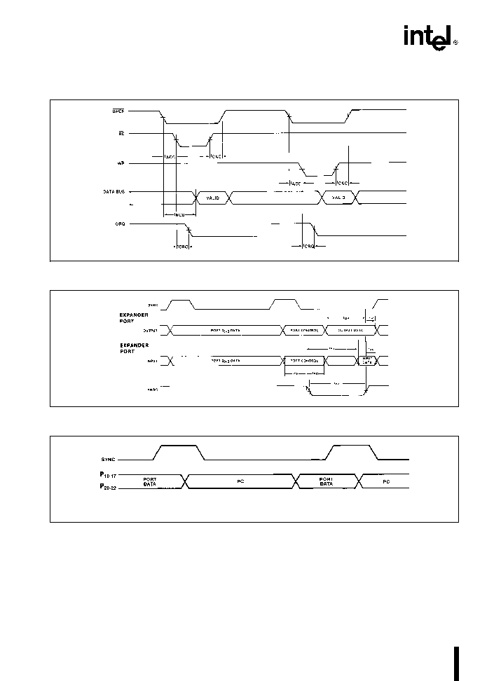
DMA
290256 ≠ 20
PORT 2
290256 ≠ 21
PORT TIMING DURING EXTERNAL ACCESS (EA)
290256 ≠ 22
On the Rising Edge of SYNC and EA is Enabled Port Data is Valid and can be Strobed on the Trailing Edge of Sync the
Program Counter Contents are Available
12
12