
Other brands and names are the property of their respective owners
Information in this document is provided in connection with Intel products Intel assumes no liability whatsoever including infringement of any patent or
copyright for sale and use of Intel products except as provided in Intel's Terms and Conditions of Sale for such products Intel retains the right to make
changes to these specifications at any time without notice Microcomputer Products may have minor variations to this specification known as errata
November 1995
COPYRIGHT
INTEL CORPORATION 1995
Order Number 270999-007
87C196KT 87C196KS
ADVANCED 16-BIT CHMOS MICROCONTROLLER
Automotive
(
b
40 Cto
a
125 C Ambient)
Y
High Performance CHMOS 16-Bit CPU
Y
Up to 32 Kbytes of On-Chip EPROM
Y
Up to 1 Kbyte of On-Chip Register RAM
Y
Up to 512 Bytes of Additional RAM
(Code RAM)
Y
Register-Register Architecture
Y
8 Channel 10-Bit A D with Sample Hold
Y
37 Prioritized Interrupt Sources
Y
Up to Seven 8-Bit (56) I O Ports
Y
Full Duplex Serial I O Port
Y
Dedicated Baud Rate Generator
Y
Interprocessor Communication Slave
Port
Y
Selectable Bus Timing Modes for
Flexible Interfacing
Y
Oscillator Fail Detection Circuitry
Y
High Speed Peripheral Transaction
Server (PTS)
Y
Two Dedicated 16-Bit High-Speed
Compare Registers
Y
10 High Speed Capture Compare (EPA)
Y
Full Duplex Synchronous Serial I O
Port (SSIO)
Y
Two Flexible 16-Bit Timer Counters
Y
Quadrature Counting Inputs
Y
Flexible 8- 16-Bit External Bus
(Programmable)
Y
Programmable Bus (HLD HLDA)
Y
1 75 ms 16 x 16 Multiply
Y
3 ms 32 16 Divide
Y
68-Pin PLCC Package
The 87C196Kx devices represents the 4th generation of MCS
96 microcontroller products implemented on
Intel's advanced 1 micron process technology These products are based on the 80C196KB device with
enhancements ideal for automotive applications The instruction set is a true super set of the 80C196KB with a
few new instructions
The MCS 96 microcontroller family members are all high performance microcontrollers with a 16-bit CPU The
87C196KT is composed of the high speed (16 MHz) KX macrocore as well as the following peripherals Up to
32 Kbytes of Program EPROM up to 1 Kbytes of Register RAM (00-3FFH including SFRs) up to 512 bytes of
code RAM (16-bit addressing modes) with the ability to execute from this RAM space an eight channel-10 Bit
g
3LSB analog to digital converter with programmable S H times with conversion times
k
20 ms at 16 MHz an
asynchronous synchronous serial I O port (8096 compatable) with a dedicated 16-bit baud rate generator an
additional synchronous serial I O port with full duplex master slave transceivers a flexible timer counter
structure with prescaler cascading and quadrature capabilities 10 modularized multiplexed high speed I O
for capture and compare (called Event Processor Array) with 250 ns resolution and double buffered inputs
and a sophisticated prioritized interrupt structure with programmable Peripheral Transaction Server (PTS) The
PTS has several channel modes including single burst block transfers from any memory location to any
memory location a PWM and PWM toggle mode to be used in conjunction with the EPA and an A D scan
mode
Additional SFR space is allocated for the EPA and can be ``windowed'' into the lower Register RAM area
NOTICE
This datasheet contains information on products in production The specifications are subject to change
without notice Verify with your local Intel Sales office that you have the latest data sheet before finalizing a
design
1

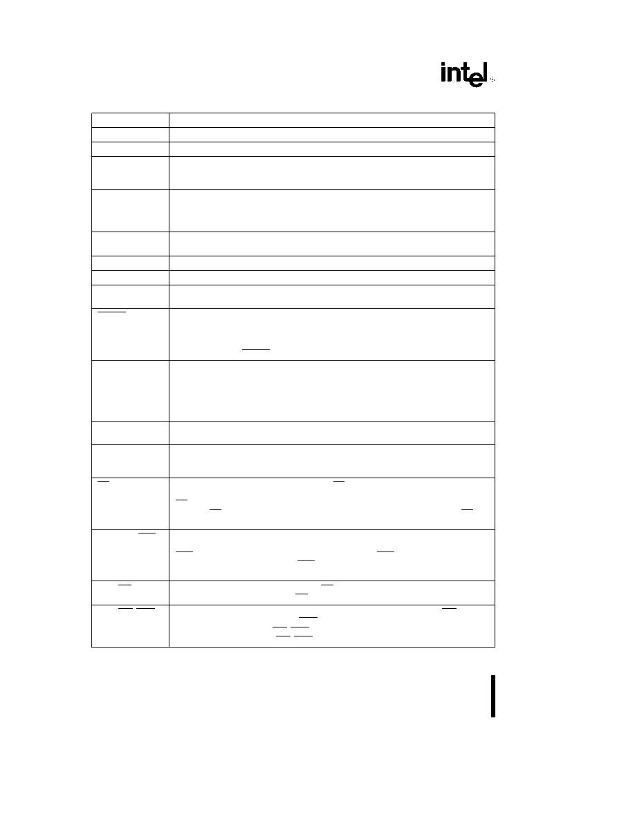
87C196KT 87C196KS
Device
Pins Package
EPROM
Reg RAM
Code RAM
I O
EPA
SIO
SSIO
A D
87C196KT
68-Pin PLCC
32K
1K
512b
56
10
Y
Y
8
87C196KS
68-Pin PLCC
24K
1K
256b
56
10
Y
Y
8
NOTE
This is a PRODUCT PREVIEW DATA SHEET The AC and DC parameters contained within this data sheet may change
after full automotive temperature characterization of the device has been performed Contact your local sales office before
finalizing the Timing and D C characteristics of a design to verify you have the latest information
ARCHITECTURE
The KT KS are new members of the MCS-96 family
having the same architecture and use the same in-
struction set as the 80C196KB Many new features
have been added including
CPU FEATURES
Y
Powerdown and Idle Modes
Y
16 MHz Operating Frequency
Y
A High Performance Peripheral
Transaction Server (PTS)
Y
37 Interrupt Vectors
Y
Up to 512 Bytes of Additional Code
RAM
Y
Up to 1 Kbyte of Additional Register
RAM
Y
``Windowing'' Allows 8-Bit Addressing
to some 16-Bit Addresses
Y
1 75 ms 16 x 16 Multiply
Y
3 ms 32 16 Divide
Y
Oscillator Fail Detect Circuitry
PERIPHERAL FEATURES
Programmable A D Conversion and S H Times
10 Capture Compare I O with 2 Flexible Timers
(250 ns Resolution and Double Buffered Inputs)
Synchronous Serial I O Port for Full Duplex Seri-
al I O
Synchronous Asynchronous
Serial
I O
Port
(with Dedicated 16-Bit Baud Rate Generator)
Total Utilization of ALL Available Pins (I O Mux'd
with Control)
(2) 16-Bit Timers with Prescale Cascading and
Quadrature Counting Capabilities
Up to 12 Externally Triggered Interrupts
NEW INSTRUCTIONS
XCH XCHB Exchange the contents of two loca-
tions either Word or Byte is support-
ed
BMOVI
Interruptable Block Move Instruction
allows the user to be interrupted dur-
ing long executing Block Moves
TIJMP
Table Indirect JUMP This instruction
incorportes a way to do complex
CASE level branches through one in-
struction An example of such code
savings several interrupt sources and
only one interrupt vector The TIJMP
instruction will sort through the sourc-
es and branch to the appropriate sub-
code level in one instruction This in-
struction was added especially for the
EPA structure but has other code sav-
ing advantages
EPTS DPTS Enable and Disable Interrupts (Works
like EI and DI)
SFR OPERATION
A total of 1 Kbyte of Register RAM is implemented
on the 87C196KT KS devices These locations sup-
port the on-chip peripherals that the 87C196KT KS
has (SFR's) as well as offering a data storage area
These locations are all 8-bit directly addressable by
use of the windowing technique Any 32- 64- or 128-
byte section can be relocated into the upper 32- 64-
or 128-byte area of the Register RAM area 080H �
0FFH
2
2
87C196KT 87C196KS
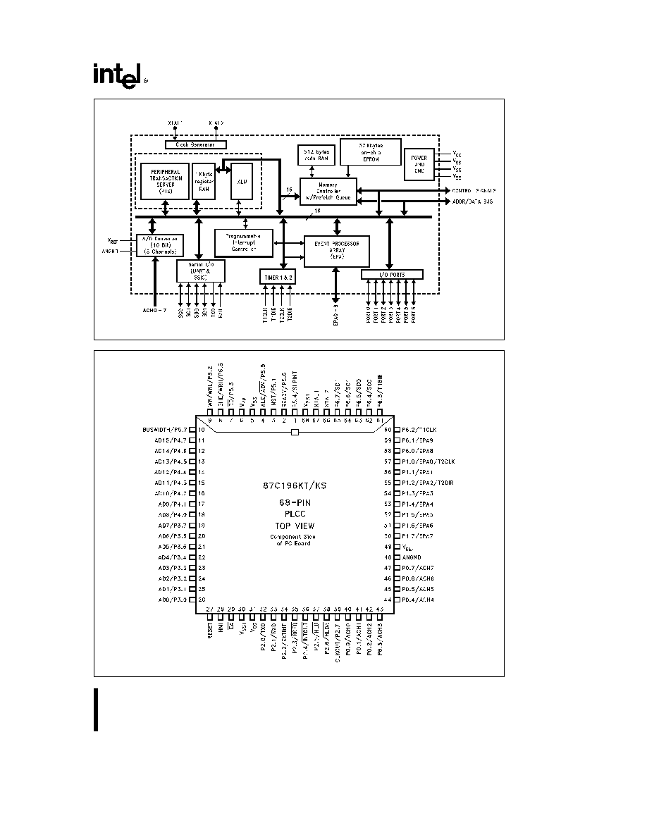
87C196KT Block Diagram
270999 � 1
270999 � 2
3
3
87C196KT 87C196KS
PIN DESCRIPTIONS
Symbol
Name and Function
V
CC
Main supply voltage (a5V)
V
SS
V
SSI
V
SSI
Digital circuit ground (0V) There are three V
SS
pins all of which MUST be connected
V
REF
Reference for the A D converter (a5V) V
REF
is also the supply voltage to the analog
portion of the A D converter and the logic used to read Port 0 Must be connected for
A D and Port 0 to function
V
PP
Programming voltage for the EPROM parts It should be a12 5V for programming It
is also the timing pin for the return from powerdown circuit Connect this pin with a
1 mF capacitor to V
SS
and a 1 MX resistor to V
CC
If this function is not used V
PP
may be tied to V
CC
ANGND
Reference ground for the A D converter Must be held at nominally the same
potential as V
SS
XTAL1
Input of the oscillator inverter and the internal clock generator
XTAL2
Output of the oscillator inverter
P2 7 CLKOUT
Output of the internal clock generator The frequency is
the oscillator frequency It
has a 50% duty cycle Also LSIO pin
RESET
Reset input to the chip Input low for at least 16 state times will reset the chip The
subsequent low to high transition resynchronizes CLKOUT and commences a 10-
state time sequence in which the PSW is cleared bytes are read from 2018H and
201AH loading the CCBs and a jump to location 2080H is executed Input high for
normal operation RESET has an internal pullup
P5 7 BUSWIDTH
Input for bus width selection If CCR bit 1 is a one and CCR1 bit 2 is a one this pin
dyamically controls the Buswidth of the bus cycle in progress If BUSWIDTH is low an
8-bit cycle occurs if BUSWIDTH is high a 16-bit cycle occurs If CCR bit 1 is ``0'' and
CCR1 bit 2 is ``1'' all bus cycles are 8-bit if CCR bit 1 is ``1'' and CCR1 bit 2 is ``0'' all
bus cycles are 16-bit CCR bit 1 e ``0'' and CCR1 bit 2 e ``0'' is illegal Also an LSIO
pin when not used as BUSWIDTH
NMI
A positive transition causes a non maskable interrupt vector through memory location
203EH
P5 1 INST
Output high during an external memory read indicates the read is an instruction fetch
INST is valid throughout the bus cycle INST is active only during external memory
fetches during internal EPROM fetches INST is held low Also LSIO when not INST
EA
Input for memory select (External Access) EA equal to a high causes memory
accesses to locations 2000H through 9FFFH to be directed to on-chip EPROM ROM
EA equal to a low causes accesses to these locations to be directed to off-chip
memory EA e a12 5V causes execution to begin in the Programming Mode EA is
latched at reset
P5 0 ALE ADV
Address Latch Enable or Address Valid output as selected by CCR Both pin options
provide a latch to demultiplex the address from the address data bus When the pin is
ADV it goes inactive (high) at the end of the bus cycle ADV can be used as a chip
select for external memory ALE ADV is active only during external memory
accesses Also LSIO when not used as ALE
P5 3 RD
Read signal output to external memory RD is active only during external memory
reads or LSIO when not used as RD
P5 2 WR WRL
Write and Write Low output to external memory as selected by the CCR WR will go
low for every external write while WRL will go low only for external writes where an
even byte is being written WR WRL is active during external memory writes Also an
LSIO pin when not used as WR WRL
4
4

87C196KT 87C196KS
PIN DESCRIPTIONS
(Continued)
Symbol
Name and Function
P5 5 BHE WRH
Byte High Enable or Write High output as selected by the CCR BHEe0 selects the
bank of memory that is connected to the high byte of the data bus A0e0 selects
that bank of memory that is connected to the low byte Thus accesses to a 16-bit
wide memory can be to the low byte only (A0e0 BHEe1) to the high byte only
(A0e1 BHEe0) or both bytes (A0e0 BHEe0) If the WRH function is selected
the pin will go low if the bus cycle is writing to an odd memory location BHE WRH is
only valid during 16-bit external memory write cycles Also an LSIO pin when not
BHE WRH
P5 6 READY
Ready input to lengthen external memory cycles for interfacing with slow or
dynamic memory or for bus sharing If the pin is high CPU operation continues in a
normal manner If the pin is low prior to the falling edge of CLKOUT the memory
controller goes into a wait state mode until the next positive transition in CLKOUT
occurs with READY high When external memory is not used READY has no effect
The max number of wait states inserted into the bus cycle is controlled by the CCR
CCR1 Also an LSIO pin when READY is not selected
P5 4 SLPINT
Dual function I O pin As a bidirectional port pin or as a system function The system
function is a Slave Port Interrupt Output Pin
P6 2 T1CLK
Dual function I O pin Primary function is that of a bidirectional I O pin however it
may also be used as a TIMER1 Clock input The TIMER1 will increment or
decrement on both positive and negative edges of this pin
P6 3 T1DIR
Dual function I O pin Primary function is that of a bidirectional I O pin however it
may also be used as a TIMER1 Direction input The TIMER1 will increment when
this pin is high and decrements when this pin is low
PORT1 EPA0 � 7
Dual function I O port pins Primary function is that of bidirectional I O System
function is that of High Speed capture and compare EPA0 and EPA2 have yet
P6 0 � 6 1 EPA8 � 9
another function of T2CLK and T2DIR of the TIMER2 timer counter
PORT 0 ACH0 � 7
8-bit high impedance input-only port These pins can be used as digital inputs and or
as analog inputs to the on-chip A D converter These pins are also used as inputs to
EPROM parts to select the Programming Mode
P6 3 � 6 7 SSIO
Dual function I O ports that have a system function as Synchronous Serial I O Two
pins are clocks and two pins are data providing full duplex capability
PORT 2
8-bit multi-functional port All of its pins are shared with other functions
PORT 3 and 4
8-bit bidirectional I O ports with open drain outputs These pins are shared with the
multiplexed address data bus which has strong internal pullups
5
5

87C196KT 87C196KS
CCB
(2018H Byte)
0
PD
e
``1'' Enables Powerdown
1
BW0
e
See Table
2
WR
e
``1'' e WR BHE - ``0'' e WRL WRH
3
ALE
e
``1'' e ALE - ``0'' e ADV
4
IRC0
e
See Table
5
IRC1
e
(
6
LOC0
e
See Table
7
LOC1
e
(
CCB1
(201AH Byte)
0
0
e
Reserved Must Be ``0''
1
IRC2
e
See Table
2
BW1
e
See Table
3
WDE
e
``0'' e Always Enabled
4
1
e
Reserved Must Be ``01''
5
0
e
(
6
MSEL0
e
See Table
7
MSEL1
e
(
LOC1
LOC0
Function
0
0
Read and Write Protected
0
1
Write Protected Only
1
0
Read Protected Only
1
1
No Protection
IRC2
IRC1
IRC0
Max Wait States
0
0
0
Zero Wait States
1
0
0
1 Wait State
1
0
1
2 Wait States
1
1
0
3 Wait States
1
1
1
INFINITE
MSEL1
MSEL0
Bus Timing Mode
0
0
Mode 0 (1-Wait KR)
0
1
Mode 1
1
0
Mode 2
1
1
Mode 3 (KR)
BW1
BW0
Bus Width
0
0
ILLEGAL
0
1
16-Bit Only
1
0
8-Bit Only
1
1
BW Pin Controlled
Mode 0
Designed to be similar to the 87C196KR bus
(1-Wait KR)
timing with 1 automatic wait state
See AC Timings section for actual timings data
Mode 1
RD WR advanced 1 T
OSC
ALE advanced 0 5 T
OSC
ALE pulse width remains 1 T
OSC
Mode 2
RD WR advanced 1 T
OSC
ALE advanced 0 5 T
OSC
ALE pulse width remains 1 T
OSC
Address advanced 0 5 T
OSC
Mode 3 (KR)
Designed to be similar to the 87C196KR bus
timing
See AC Timings section for actual timings data
6
6
87C196KT 87C196KS
ABSOLUTE MAXIMUM RATINGS
Storage Temperature
b
60 C to a150 C
Voltage from V
PP
or EA to
V
SS
or ANGND
b
0 5V to a13 0V
Voltage from Any Other Pin
to V
SS
or ANGND
b
0 5 to a7 0V
This includes V
PP
on ROM and CPU devices
Power Dissipation
0 5W
NOTICE This is a production data sheet The specifi-
cations are subject to change without notice
WARNING Stressing the device beyond the ``Absolute
Maximum Ratings'' may cause permanent damage
These are stress ratings only Operation beyond the
``Operating Conditions'' is not recommended and ex-
tended exposure beyond the ``Operating Conditions''
may affect device reliability
OPERATING CONDITIONS
Symbol
Parameter
Min
Max
Units
T
A
Ambient Temperature Under Bias
b
40
a
125
C
V
CC
Digital Supply Voltage
4 50
5 50
V
V
REF
Analog Supply Voltage
4 50
5 50
V
F
OSC
Oscillator Frequency
4
16
MHz (Note 4)
NOTE
ANGND and V
SS
should be nominally at the same potential
DC CHARACTERISTICS
(Under Listed Operating Conditions)
Symbol
Parameter
Test Conditions
Min
Typ
Max
Units
I
CC
V
CC
Supply Current
XTAL1
e
16 MHz
82
mA
(
b
40 C to
a
125 C Ambient)
V
CC
e
V
PP
e
V
REF
e
5 5V
I
REF
A D Reference Supply Current
(While device in Reset)
5
mA
I
IDLE
Idle Mode Current
XTAL1
e
16 MHz
40
mA
V
CC
e
V
PP
e
V
REF
e
5 5V
I
PD
Powerdown Mode Current
V
CC
e
V
PP
e
V
REF
e
5 5V
(6 9)
50
TBD
m
A
V
IL
Input Low Voltage (all pins)
For PORT0
(8)
b
0 5V
0 3 V
CC
V
V
IH
Input High Voltage
For PORT0
(8)
0 7 V
CC
V
CC
a
0 5
V
V
IH1
Input High Voltage XTAL1
XTAL1 Input Pin Only
(1)
0 7 V
CC
V
CC
a
0 5
V
V
IH2
Input High Voltage on RESET
RESET input pin only
0 7 V
CC
V
CC
a
0 5
V
7
7
87C196KT 87C196KS
DC CHARACTERISTICS
(Under Listed Operating Conditions) (Continued)
Symbol
Parameter
Test Conditions
Min
Typ
Max
Units
V
OL
Output Low Voltage
I
OL
e
200 mA
(3 5)
0 3
V
(Outputs Configured as
I
OL
e
3 2 mA
0 45
V
Complementary)
I
OL
e
7 0 mA
1 5
V
V
OH
Output High Voltage
I
OH
e b
200 mA
(3 5)
V
CC
b
0 3
V
(Outputs Configured as
I
OH
e b
3 2 mA
V
CC
b
0 7
V
Complementary)
I
OH
e b
7 0 mA
V
CC
b
1 5
V
I
LI
Input Leakage Current (Std Inputs)
V
SS
k
V
IN
k
V
CC
g
10
m
A
I
LI1
Input Leakage Current (Port 0)
V
SS
k
V
IN
k
V
REF
g
1 5
m
A
V
OH1
SLPINT (P5 4) and HLDA (P2 6)
I
OH
e
0 8 mA
(7)
2 0
V
Output High Voltage in RESET
V
OH2
Output High Voltage in RESET
I
OH
e b
15 mA
(1 8)
V
CC
b
1V
V
I
OH2
Output High Current in RESET
V
OH2
e
V
CC
b
1 0V
b
30
b
120
m
A
V
OH2
e
V
CC
b
2 5V
b
75
b
240
m
A
V
OH2
e
V
CC
b
4 0V
b
90
b
280
m
A
C
S
Pin Capacitance (Any pin to V
SS
)
f
test
e
1 0 MHz
(6)
10
pF
V
OL3
Output Low Voltage in RESET
I
OL3
e
4 mA
(10)
0 3
(RESET Pin Only)
I
OL3
e
6 mA
0 5
V
I
OL3
e
8 mA
0 8
R
WPU
Weak Pullup Resistance
(Note 6)
150K
X
R
RST
Reset Pullup Resistor
65K
180K
X
NOTES
1 All BD (bidirectional) pins except INST and CLKOUT INST and CLKOUT are excluded due to their not being weakly
pulled high in reset BD pins include Port1 Port2 Port3 Port4 Port5 and Port6 except SPLINT (P5 4) and HLDA (P2 6)
2 Standard input pins include XTAL1 EA RESET and Port 1 2 5 6 when setup as inputs
3 All bidirectional I O pins when configured as Outputs (Push Pull)
4 Device is static and should operate below 1 Hz but only tested down to 4 MHz
5 Maximum I
OL
I
OH
currents per pin will be characterized and published at a later date
6 Typicals are based on limited number of samples and are not guaranteed The values listed are at room temperature and
V
REF
e
V
CC
e
5 0V
7 Violating these specifications in reset may cause the device to enter test modes (P5 4 and P2 6)
8 When P0 is used as analog inputs refer to A D specifications for this characteristic
9 For temperatures
k
100 C typical is 10 mA
10 This specification is not tested in production and is based upon theoretical estimates and or product characterization
I
CC
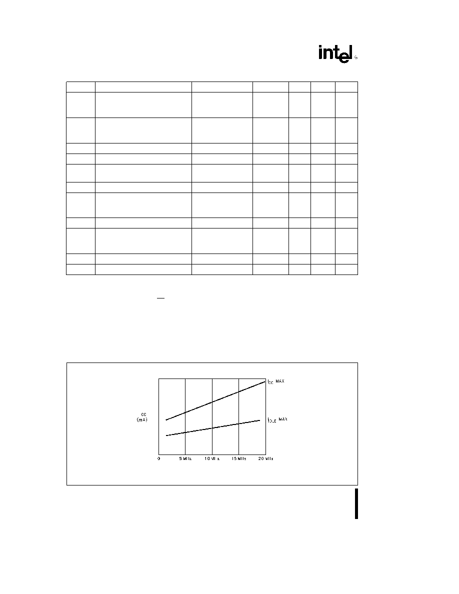
vs Frequency
270999 � 24
NOTES
I
CC
Max
e
3 25
c
Freq
a
30
I
IDLE
Max
e
1 25
c
Freq
a
20
8
8

87C196KT 87C196KS
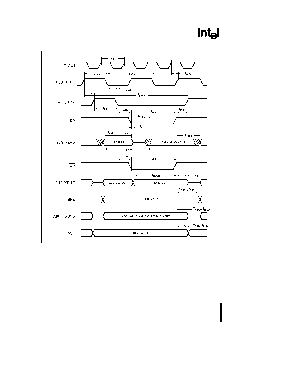
AC CHARACTERISTICS
(Over Specified Operating Conditions)
Test Conditions Capacitance Load on All Pins e 100 pF Rise and Fall Times e 10 ns
The 87C196KT will meet these specifications
Symbol
Parameter
Min
Max
Units
F
XTAL
Frequency on XTAL1
4 0
16 0
MHz
(1)
T
OSC
XTAL1 Period (1 F
XTAL
)
62 5
250
ns
T
XHCH
XTAL1 High to CLKOUT High or Low
a
20
110
ns
T
OFD
Clock Failure to Reset Pulled Low
(6)
4
40
m
s
T
CLCL
CLKOUT Period
2 T
OSC
ns
T
CHCL
CLKOUT High Period
T
OSC
b
10
T
OSC
a
30
ns
T
CLLH
CLKOUT Low to ALE ADV High
b
10
a
15
ns
T
LLCH
ALE ADV Low to CLKOUT High
b
25
a
15
ns
T
LHLH
ALE ADV Cycle Time
4 T
OSC
ns
(5)
T
LHLL
ALE ADV High Time
T
OSC
b
10
T
OSC
a
10
ns
T
AVLL
Address Valid to ALE Low
T
OSC
b
15
ns
T
LLAX
Address Hold After ALE ADV Low
T
OSC
b
40
ns
T
LLRL
ALE ADV Low to RD Low
T
OSC
b
40
ns
T
RLCL
RD Low to CLKOUT Low
b
5
a
35
ns
T
RLRH
RD Low Period
T
OSC
b
5
ns
(5)
T
RHLH
RD High to ALE ADV High
T
OSC
T
OSC
a
25
ns
(3)
T
RLAZ
RD Low to Address Float
a
5
ns
T
LLWL
ALE ADV Low to WR Low
T
OSC
b
10
ns
T
CLWL
CLKOUT Low to WR Low
b
10
a
25
ns
T
QVWH
Data Valid before WR High
T
OSC
b
23
ns
T
CHWH
CLKOUT High to WR High
b
10
a
15
ns
T
WLWH
WR Low Period
T
OSC
b
30
ns
(5)
T
WHQX
Data Hold after WR High
T
OSC
b
30
ns
T
WHLH
WR High to ALE ADV High
T
OSC
b
10
T
OSC
a
15
ns
(3)
T
WHBX
BHE INST Hold after WR High
T
OSC
b
10
ns
T
WHAX
AD8 � 15 Hold after WR High
T
OSC
b
30
ns
(4)
T
RHBX
BHE INST Hold after RD High
T
OSC
b
10
ns
T
RHAX
AD8 � 15 Hold after RD High
T
OSC
b
30
ns
(4)
NOTES
1 Testing performed at 4 0 MHz however the device is static by design and will typically operate below 1 Hz
2 Typical specifications not guaranteed
3 Assuming back-to-back bus cycles
4 8-bit bus only
5 If wait states are used add 2 Tosc
c
n where n
e
number of wait states If mode 0 (1 automatic wait state added)
operation is selected add 2 T
OSC
to specification
6 T
OFD
is the time for the oscillator fail detect circuit (OFD) to react to a clock failure The OFD circuitry is enabled by
programming the UPROM location 0778H with the value 0004H KT KS customer QROM codes need to equate location
2016H to the value 0CDEH if the oscillator fail detect (OFD) function is desired Intel manufacturing uses location 2016H
as a flag to determine whether or not to program the Clock Detect Enable (CDE) bit Programming the CDE bit
enables oscillator fail detection
9
9

87C196KT 87C196KS
AC CHARACTERISTICS
(Over Specified Operating Conditions)
Test Conditions Capacitance Load on All Pins e 100 pF Rise anf Fall Times e 10 ns
The system must meet these specifications to work with the 87C196KT
Symbol
Parameter
Min
Max
Units
T
AVYV
Address Valid to Ready Setup
2 T
OSC
b
75
ns
(3)
T
LLYV
ALE Low to READY Setup
T
OSC
b
70
ns
(3)
T
YLYH
Non READY Time
No Upper Limit
ns
T
CLYX
READY Hold after CLKOUT Low
0
T
OSC
b
30
ns
(1)
T
AVGV
Address Valid to BUSWIDTH Setup
2 T
OSC
b
75
ns
(2 3)
T
LLGV
ALE Low to BUSWIDTH Setup
T
OSC
b
60
ns
(2 3)
T
CLGX
BUSWIDTH Hold after CLKOUT Low
0
ns
T
AVDV
Address Valid to Input Data Valid
3 T
OSC
b
55
ns
(2)
T
RLDV
RD active to input Data Valid
T
OSC
b
30
ns
(2)
T
CLDV
CLKOUT Low to Input Data Valid
T
OSC
b
60
ns
T
RHDZ
End of RD to Input Data Float
T
OSC
ns
T
RHDX
Data Hold after RD High
0
ns
NOTES
1 If Max is exceeded additional wait states will occur
2 If wait states are used add 2 Tosc
c
n where n
e
number of wait states
3 If mode 0 is selected one wait state minimum is always added If additional wait states are required add 2 Tosc to the
specification
10
10

87C196KT 87C196KS
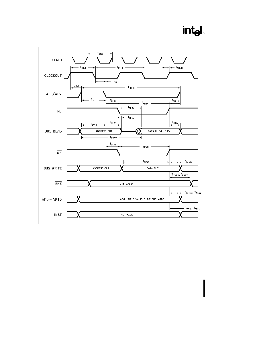
87C196KT SYSTEM BUS TIMING
270999 � 4
If mode 0 operation is selected add 2 Tosc to this time
11
11

87C196KT 87C196KS
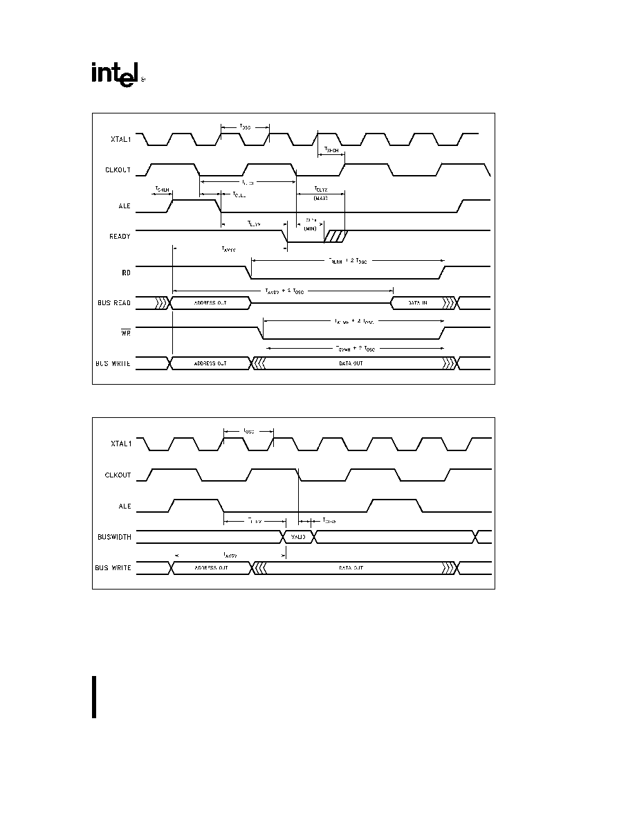
87C196KT READY TIMINGS (ONE WAIT STATE)
270999 � 5
If mode 0 selected one wait state is always added If additional wait states are required add 2 Tosc to these specifica-
tions
87C196KT BUSWIDTH TIMINGS
270999 � 6
If mode 0 selected add 2 Tosc to these specifications
12
12
87C196KT 87C196KS
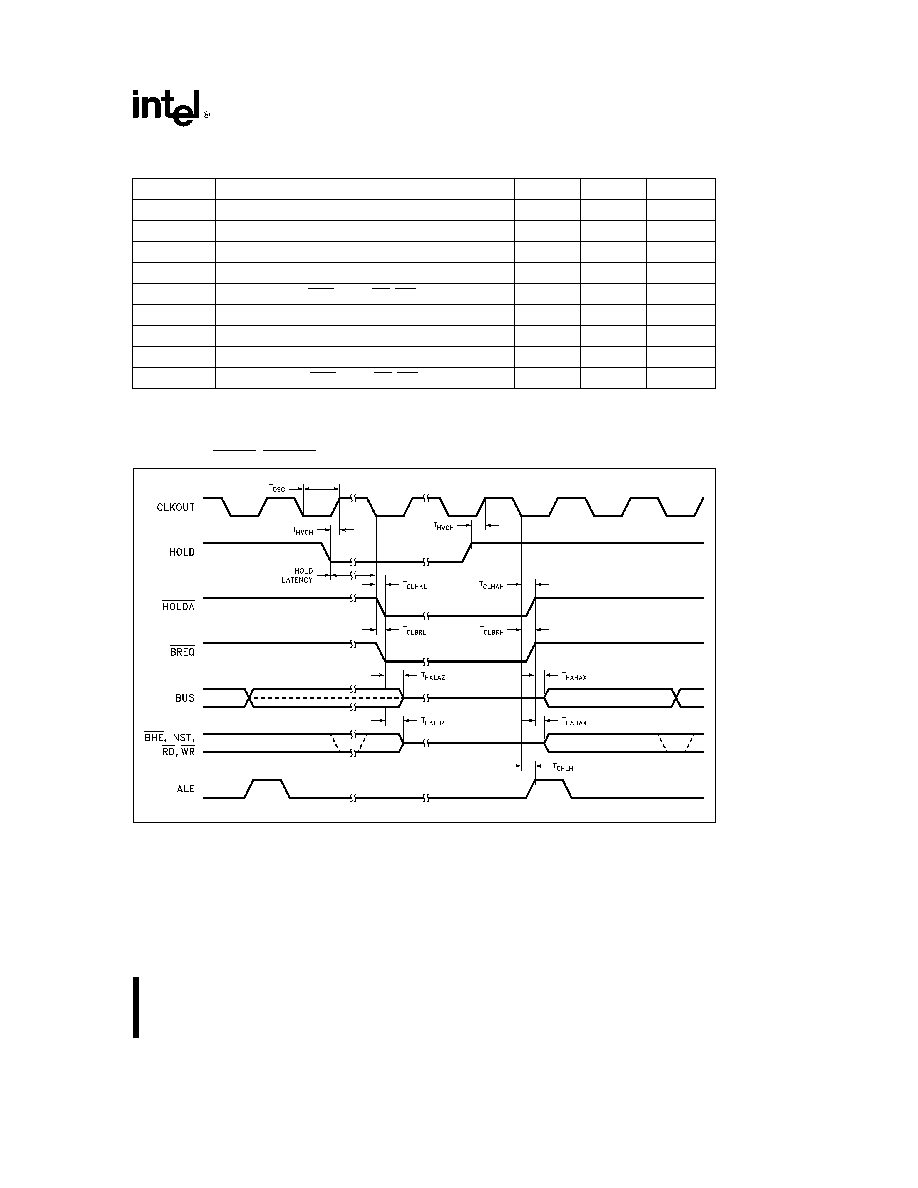
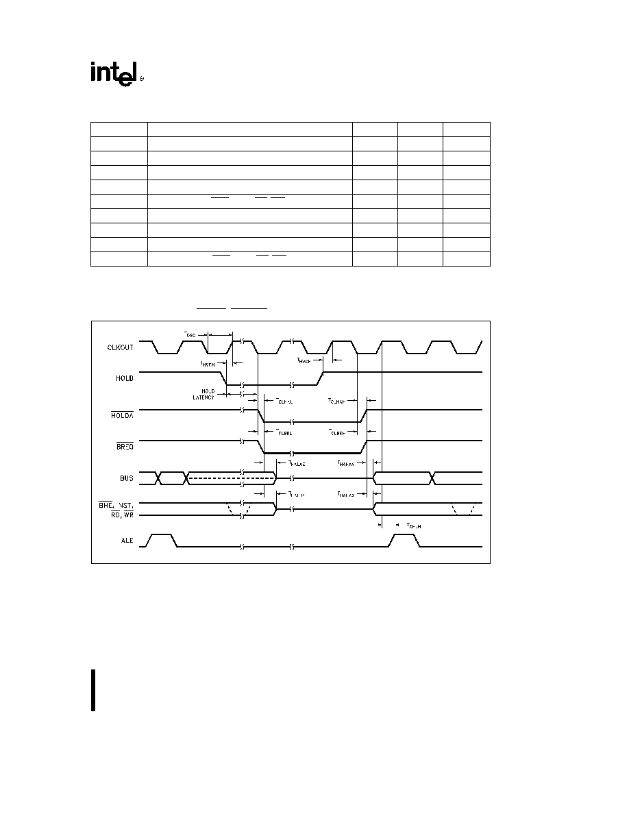
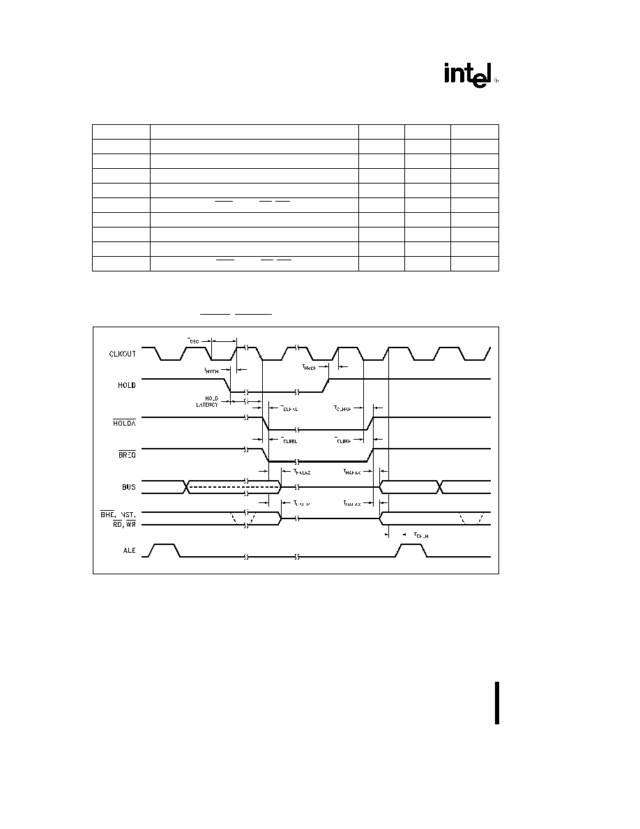
HOLD HOLDA TIMINGS
(Over Specified Operation Conditions)
Test Conditions Capacitance Load on All Pins e 100 pF Rise and Fall Times e 10 ns
Symbol
Parameter
Min
Max
Units
T
HVCH
HOLD Setup Time
a
65
ns
(1)
T
CLHAL
CLKOUT Low to HLDA Low
b
15
a
15
ns
T
CLBRL
CLKOUT Low to BREQ Low
b
15
a
15
ns
T
AZHAL
HLDA Low to Address Float
a
20
ns
T
BZHAL
HLDA Low to BHE INST RD WR Weakly Driven
a
25
ns
T
CLHAH
CLKOUT Low to HLDA High
b
25
a
15
ns
T
CLBRH
CLKOUT Low to BREQ High
b
25
a
25
ns
T
HAHAX
HLDA High to Address No Longer Float
b
15
ns
T
HAHBV
HLDA High to BHE INST RD WR Valid
b
10
a
15
ns
NOTE
1 To guarantee recognition at next clock
8XC196KT HOLD HOLDA TIMINGS
270999 � 7
13
13
87C196KT 87C196KS
BUS MODE 1
AC CHARACTERISTICS
(Over Specified Operating Conditions)
Test Conditions Capacitance Load on All Pins e 100 pF Rise and Fall Times e 10 ns
The 87C196KT will meet these specifications
Symbol
Parameter
Min
Max
Units
F
XTAL
Frequency on XTAL1
8 0
16 0
MHz
(1)
T
OSC
XTAL1 Period (1 F
XTAL
)
62 5
125
ns
T
XHCH
XTAL1 High to CLKOUT High or Low
a
20
110
ns
T
CLCL
CLKOUT Period
2 T
OSC
ns
T
CHCL
CLKOUT High Period
T
OSC
b
10
T
OSC
a
27
ns
T
CHLH
CLKOUT HIGH to ALE ADV High
0 5 T
OSC
b
15
0 5 T
OSC
a
20
ns
T
CLLL
CLKOUT LOW to ALE ADV Low
0 5 T
OSC
b
25
0 5 T
OSC
a
15
ns
T
LHLH
ALE ADV Cycle Time
4 T
OSC
ns
(5)
T
LHLL
ALE ADV High Time
T
OSC
b
10
T
OSC
a
10
ns
T
AVLL
Address Valid to ALE Low
0 5 T
OSC
b
15
ns
T
LLAX
Address Hold After ALE ADV Low
0 5 T
OSC
b
20
ns
T
LLRL
ALE ADV Low to RD Low
0 5 T
OSC
b
30
ns
T
RLCL
RD Low to CLKOUT Low
T
OSC
b
10
T
OSC
a
30
ns
T
RLRH
RD Low Period
2 T
OSC
b
20
ns
(5)
T
RHLH
RD High to ALE ADV High
0 5 T
OSC
0 5 T
OSC
a
25
ns
(3)
T
RLAZ
RD Low to Address Float
a
5
ns
T
LLWL
ALE ADV Low to WR Low
0 5 T
OSC
b
10
ns
T
CLWL
CLKOUT Low to WR Low
T
OSC
b
15
T
OSC
a
25
ns
T
QVWH
Data Valid before WR High
2 T
OSC
b
23
ns
T
CHWH
CLKOUT High to WR High
b
10
a
15
ns
T
WLWH
WR Low Period
2 T
OSC
b
15
ns
(5)
T
WHQX
Data Hold after WR High
0 5 T
OSC
b
25
ns
T
WHLH
WR High to ALE ADV High
0 5 T
OSC
b
10
0 5 T
OSC
a
15
ns
(3)
T
WHBX
BHE Hold after WR High
T
OSC
b
15
ns
T
WHIX
INST Hold after WR High
0 5 T
OSC
b
15
T
WHAX
AD8 � 15 Hold after WR High
0 5 T
OSC
b
30
ns
(4)
T
RHBX
BHE Hold after RD High
T
OSC
b
32
ns
T
RHAX
AD8 � 15 Hold after RD High
0 5 T
OSC
b
32
T
RHAX
AD8 � 15 Hold after RD High
0 5 T
OSC
b
30
ns
(4)
NOTES
1 Testing performed at 8 0 MHz however the device is static by design and will typically operate below 1 Hz
2 Typical specifications not guaranteed
3 Assuming back-to-back bus cycles
4 8-bit bus only
5 If wait states are used add 2 T
OSC
c
n where n
e
number of wait states
14
14

87C196KT 87C196KS
BUS MODE 1
AC CHARACTERISTICS
(Over Specified Operating Conditions) (Continued)
Test Conditions Capacitance Load on All Pins e 100 pF Rise and Fall Times e 10 ns
The system must meet these specifications to work with the 87C196KT
Symbol
Parameter
Min
Max
Units
T
AVYV
Address Valid to Ready Setup
2 T
OSC
b
75
ns
T
LLYV
ALE Low to READY Setup
1 5 T
OSC
b
70
ns
T
YLYH
Non READY Time
No Upper Limit
ns
T
CLYX
READY Hold after CLKOUT Low
0
T
OSC
b
30
ns
(1)
T
AVGV
Address Valid to BUSWIDTH Setup
2 T
OSC
b
75
ns
T
LLGV
ALE Low to BUSWIDTH Setup
1 5 T
OSC
b
60
ns
T
CLGX
BUSWIDTH Hold after CLKOUT Low
0
ns
T
AVDV
Address Valid to Input Data Valid
3 T
OSC
b
65
ns
(2)
T
RLDV
RD active to input Data Valid
2 T
OSC
b
44
ns
(2)
T
CLDV
CLKOUT Low to Input Data Valid
T
OSC
b
60
ns
T
RHDZ
End of RD to Input Data Float
T
OSC
ns
T
RHDX
Data Hold after RD High
0
ns
NOTES
1 If Max is exceeded additional wait states will occur
2 If wait states are used add 2 T
OSC
c
n where n
e
number of wait states If mode 0 (1 automatic wait state added)
operation is selected add 2 T
OSC
to specification
15
15
87C196KT 87C196KS
MODE 1
87C196KT SYSTEM BUS TIMING
270999 � 23
16
16
87C196KT 87C196KS
BUS MODE 1
HOLD HOLDA TIMINGS
(Over Specified Operation Conditions)
Test Conditions Capacitance Load on All Pins e 100 pF Rise and Fall Times e 10 ns
Symbol
Parameter
Min
Max
Units
T
HVCH
HOLD Setup Time
a
65
ns
(1)
T
CLHAL
CLKOUT Low to HLDA Low
b
15
a
15
ns
T
CLBRL
CLKOUT Low to BREQ Low
b
15
a
15
ns
T
AZHAL
HLDA Low to Address Float
a
25
ns
T
BZHAL
HLDA Low to BHE INST RD WR Weakly Driven
a
25
ns
T
CLHAH
CLKOUT Low to HLDA High
b
25
a
15
ns
T
CLBRH
CLKOUT Low to BREQ High
b
25
a
15
ns
T
HAHAX
HLDA High to Address No Longer Float
b
15
ns
T
HAHBV
HLDA High to BHE INST RD WR Valid
b
10
ns
NOTE
1 To guarantee recognition at next clock
MODE 1
8XC196KT HOLD HOLDA TIMINGS
270999 � 11
17
17

87C196KT 87C196KS
BUS MODE 2
AC CHARACTERISTICS
(Over Specified Operating Conditions)
Test Conditions Capacitance Load on All Pins e 100 pF Rise and Fall Times e 10 ns
The 87C196KT will meet these specifications
Symbol
Parameter
Min
Max
Units
F
XTAL
Frequency on XTAL1
8 0
16 0
MHz
(1)
T
OSC
XTAL1 Period (1 F
XTAL
)
62 5
125
ns
T
XHCH
XTAL1 High to CLKOUT High or Low
a
20
a
85
ns
T
CLCL
CLKOUT Period
2 T
OSC
ns
T
CHCL
CLKOUT High Period
T
OSC
b
10
T
OSC
a
27
ns
T
CHLH
CLKOUT HIGH to ALE ADV High
0 5 T
OSC
b
15
0 5 T
OSC
a
20
ns
T
CLLL
CLKOUT LOW to ALE ADV Low
0 5 T
OSC
b
25
0 5 T
OSC
a
15
ns
T
LHLH
ALE ADV Cycle Time
4 T
OSC
ns
(5)
T
LHLL
ALE ADV High Time
T
OSC
b
10
T
OSC
a
10
ns
T
AVLL
Address Valid to ALE Low
T
OSC
b
15
ns
T
LLAX
Address Hold After ALE ADV Low
0 5 T
OSC
b
20
ns
T
LLRL
ALE ADV Low to RD Low
0 5 T
OSC
b
30
ns
T
RLCL
RD Low to CLKOUT Low
T
OSC
b
10
T
OSC
a
30
ns
T
RLRH
RD Low Period
2 T
OSC
b
20
ns
(5)
T
RHLH
RD High to ALE ADV High
0 5 T
OSC
b
5
0 5 T
OSC
a
25
ns
(3)
T
RLAZ
RD Low to Address Float
a
5
ns
T
LLWL
ALE ADV Low to WR Low
0 5 T
OSC
b
10
ns
T
CLWL
CLKOUT Low to WR Low
T
OSC
b
22
T
OSC
a
25
ns
T
QVWH
Data Valid before WR High
2 T
OSC
b
25
ns
T
CHWH
CLKOUT High to WR High
b
10
a
15
ns
T
WLWH
WR Low Period
2 T
OSC
b
20
ns
(5)
T
WHQX
Data Hold after WR High
0 5 T
OSC
b
25
ns
T
WHLH
WR High to ALE ADV High
0 5 T
OSC
b
10
0 5 T
OSC
a
10
ns
(3)
T
WHBX
BHE Hold after WR High
T
OSC
b
15
ns
T
WHIX
INST Hold after WR High
0 5 T
OSC
b
15
T
WHAX
AD8 � 15 Hold after WR High
0 5 T
OSC
b
30
ns
(4)
T
RHBX
BHE Hold after RD High
T
OSC
b
32
ns
T
RHIX
INST Hold after RD High
0 5 T
OSC
b
32
T
RHAX
AD8 � 15 Hold after RD High
0 5 T
OSC
b
30
ns
(4)
NOTES
1 Testing performed at 8 0 MHz however the device is static by design and will typically operate below 1 Hz
2 Typical specifications not guaranteed
3 Assuming back-to-back bus cycles
4 8-bit bus only
5 If wait states are used add 2 T
OSC
c
n where n
e
number of wait states
18
18

87C196KT 87C196KS
BUS MODE 2
AC CHARACTERISTICS
(Over Specified Operating Conditions)
Test Conditions Capacitance Load on All Pins e 100 pF Rise and Fall Times e 10 ns
The system must meet these specifications to work with the 87C196KT
Symbol
Parameter
Min
Max
Units
T
AVYV
Address Valid to Ready Setup
2 5 T
OSC
b
75
ns
T
LLYV
ALE Low to READY Setup
1 5 T
OSC
b
70
ns
T
YLYH
Non READY Time
No Upper Limit
ns
T
CLYX
READY Hold after CLKOUT Low
0
T
OSC
b
30
ns
(1)
T
AVGV
Address Valid to BUSWIDTH Setup
2 5 T
OSC
b
75
ns
T
LLGV
ALE Low to BUSWIDTH Setup
1 5 T
OSC
b
60
ns
T
CLGX
BUSWIDTH Hold after CLKOUT Low
0
ns
T
AVDV
Address Valid to Input Data Valid
3 5 T
OSC
b
60
ns
(2)
T
RLDV
RD active to Input Data Valid
2 T
OSC
b
44
ns
(2)
T
CLDV
CLKOUT Low to Input Data Valid
T
OSC
b
60
ns
T
RHDZ
End of RD to Input Data Float
0 5 T
OSC
ns
T
RHDX
Data Hold after RD High
0
ns
NOTES
1 If Max is exceeded additional wait states will occur
2 If wait states are used add 2 T
OSC
c
n where n
e
number of wait states If mode 0 (1 automatic wait state added)
operation is selected add 2 T
OSC
to specification
19
19
87C196KT 87C196KS
MODE 2
87C196KT SYSTEM BUS TIMING
270999 � 12
20
20
87C196KT 87C196KS
MODE 2
87C196KT READY TIMINGS (ONE WAIT STATE)
270999 � 13
MODE 2
87C196KT BUSWIDTH TIMINGS
270999 � 14
21
21
87C196KT 87C196KS
BUS MODE 2
HOLD HOLDA TIMINGS
(Over Specified Operation Conditions)
Test Conditions Capacitance Load on All Pins e 100 pF Rise and Fall Times e 10 ns
Symbol
Parameter
Min
Max
Units
T
HVCH
HOLD Setup Time
a
65
ns
(1)
T
CLHAL
CLKOUT Low to HLDA Low
b
15
a
15
ns
T
CLBRL
CLKOUT Low to BREQ Low
b
15
a
15
ns
T
AZHAL
HLDA Low to Address Float
a
25
ns
T
BZHAL
HLDA Low to BHE INST RD WR Weakly Driven
a
25
ns
T
CLHAH
CLKOUT Low to HLDA High
b
25
a
15
ns
T
CLBRH
CLKOUT Low to BREQ High
b
25
a
15
ns
T
HAHAX
HLDA High to Address No Longer Float
b
15
ns
T
HAHBV
HLDA High to BHE INST RD WR Valid
b
10
ns
NOTE
1 To guarantee recognition at next clock
MODE 2
8XC196KT HOLD HOLDA TIMINGS
270999 � 15
22
22

87C196KT 87C196KS
AC CHARACTERISTICS
SLAVE PORT
SLAVE PORT WAVEFORM
(SLPL e 0)
270999 � 8
SLAVE PORT TIMING
(SLPL e 0 1 2 3)
Symbol
Parameter
Min
Max
Units
T
SAVWL
Address Valid to WR Low
50
ns
T
SRHAV
RD High to Address Valid
60
ns
T
SRLRH
RD Low Period
T
OSC
ns
T
SWLWH
WR Low Period
T
OSC
ns
T
SRLDV
RD Low to Output Data Valid
60
ns
T
SDVWH
Input Data Setup to WR High
20
ns
T
SWHQX
WR High to Data Invalid
30
ns
T
SRHDZ
RD High to Data Float
15
ns
NOTES
1 Test Conditions F
OSC
e
16 MHz T
OSC
e
60 ns Rise Fall Time
e
10 ns Capacitive Pin Load
e
100 pF
2 These values are not tested in production and are based upon theoretical estimates and or laboratory tests
3 Specifications above are advanced information and are subject to change
23
23
87C196KT 87C196KS
AC CHARACTERISTICS
SLAVE PORT
(Continued)
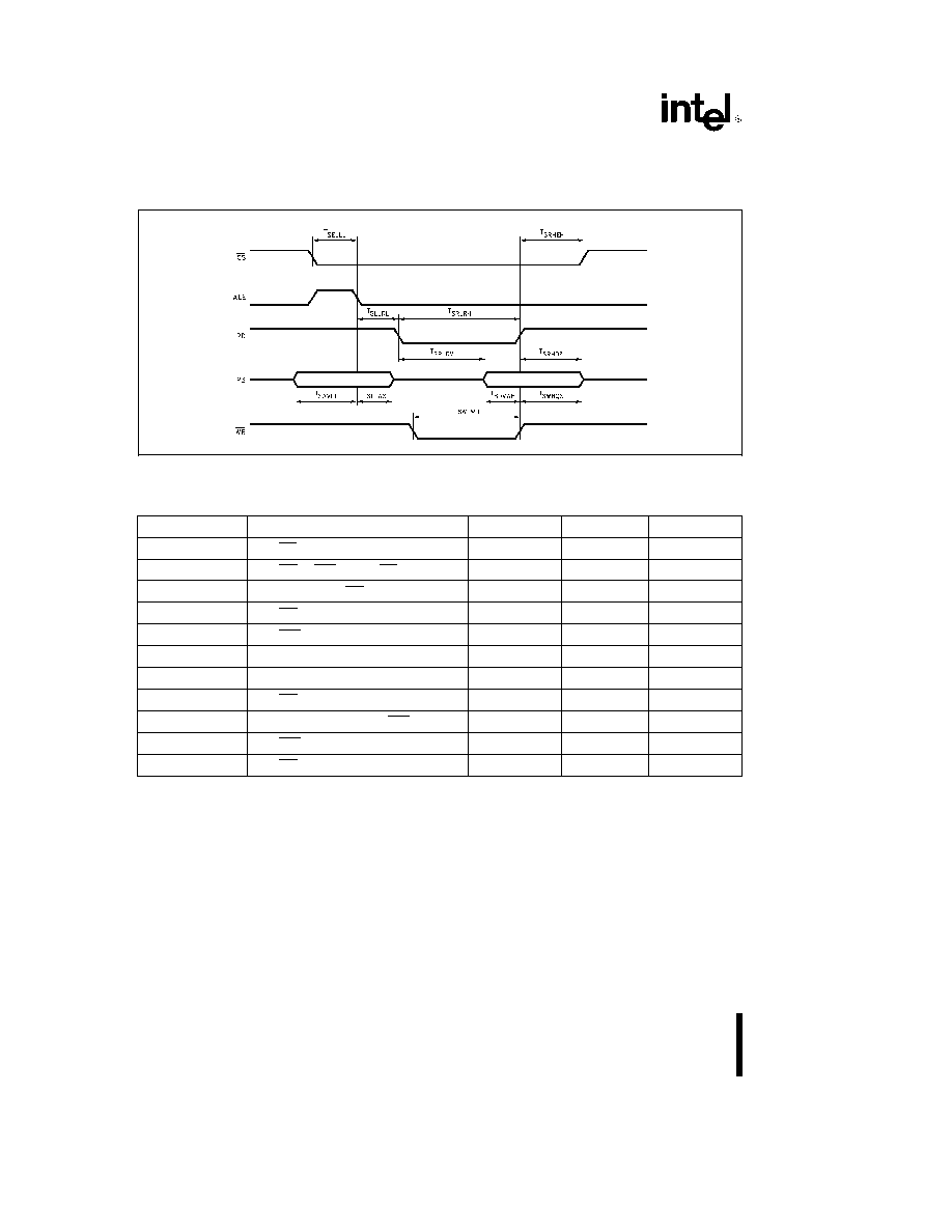
SLAVE PORT WAVEFORM
(SLPL e 1)
270999 � 9
SLAVE PORT TIMING
(SLPL e 1 2 3)
Symbol
Parameter
Min
Max
Units
T
SELLL
CS Low to ALE Low
20
ns
T
SRHEH
RD or WR High to CS High
60
ns
T
SLLRL
ALE Low to RD Low
T
OSC
ns
T
SRLRH
RD Low Period
T
OSC
ns
T
SWLWH
WR Low Period
T
OSC
ns
T
SAVLL
Address Valid to ALE Low
20
ns
T
SLLAX
ALE Low to Address Invalid
20
ns
T
SRLDV
RD Low to Output Data Valid
60
ns
T
SDVWH
Input Data Setup to WRHigh
20
ns
T
SWHQX
WR High to Data Invalid
30
ns
T
SRHDZ
RD High to Data Float
15
ns
NOTES
1 Test Conditions F
OSC
e
16 MHz T
OSC
e
60 ns Rise Fall Time
e
10 ns Capacitive Pin Load
e
100 pF
2 These values are not tested in production and are based upon theoretical estimates and or laboratory tests
3 Specifications above are advanced information and are subject to change
24
24
87C196KT 87C196KS
EXTERNAL CLOCK DRIVE
Symbol
Parameter
Min
Max
Units
1 T
XLXL
Oscillator Frequency
4
16
MHz
T
XLXL
Oscillator Period (T
OSC
)
62 5
250
ns
T
XHXX
High Time
0 35
c
T
OSC
0 65 T
OSC
ns
T
XLXX
Low Time
0 35
c
T
OSC
0 65 T
OSC
ns
T
XLXH
Rise Time
10
ns
T
XHXL
Fall Time
10
ns
EXTERNAL CLOCK DRIVE WAVEFORMS
270999 � 16
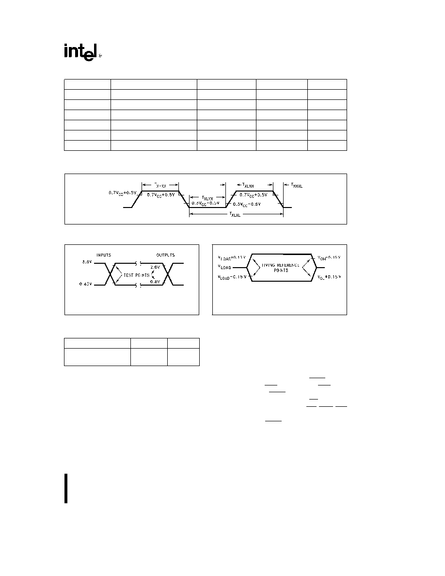
AC TESTING INPUT OUTPUT WAVEFORMS
270999 � 17
AC Testing inputs are driven at 3 5V for a logic ``1'' and
0 45V for a logic ``0'' Timing measurements are made
at 2 0V for a logic ``1'' and 0 8V for logic ``0''
FLOAT WAVEFORMS
270999 � 18
For timing purposes a Port Pin is no longer floating
when a 150 mV change from load voltage occurs and
begins to float when a 150 mV change from the loading
V
OH
V
OL
level occurs I
OL
I
OH
s
15 mA
THERMAL CHARACTERISTICS
Device and Package
i
JA
i
JC
AN87C196KT KS
36 5 C W
13 C W
(68-Lead PLCC)
NOTES
1 i
JA
e
Thermal resistance between junction and the sur-
rounding environmental (ambient) Measurements are tak-
en 1 ft away from case in air flow environment i
JC
e
Thermal resistance between junction and package surface
(case)
2 All values of i
JA
and i
JC
may fluctuate depending on
the environment (with or without airflow and how much air-
flow) and device power dissipation at temperature of oper-
ation Typical variations are
g
2 C W
3 Values listed are at a maximum power dissipation of
0 50W
EXPLANATION OF AC SYMBOLS
Each symbol is two pairs of letters prefixed by ``T''
for time The characters in a pair indicate a signal
and its condition respectively Symbols represent
the time between the two signal condition points
Conditions
Signals
H
High
A
Address
HA
HLDA
L
Low
B
BHE
L
ALE ADV
V
Valid
BR
BREQ
Q
Data Out
X
No Longer
C
CLKOUT
RD
RD
Valid
D
DATA
W
WR WRH WRI
Z
Floating
G
Buswidth
X
XTAL1
H
HOLD
Y
READY
25
25
87C196KT 87C196KS
EPROM SPECIFICATIONS
AC EPROM PROGRAMMING CHARACTERISTICS
Operating Conditions Load Capacitance e 150 pF T
C
e
25 C
g
5 C V
CC
V
REF
e
5 0V
g
0 5V V
SS
ANGND e 0V
V
PP
e
12 5V
g
0 25V EA e 12 5V
g
0 25V Fosc e 5 0 MHz
Symbol
Paramter
Min
Max
Units
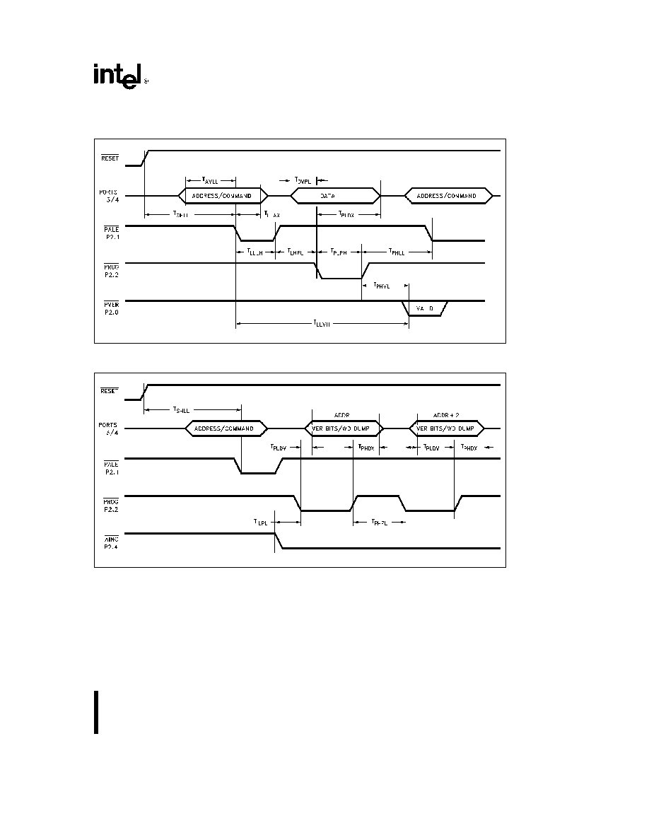
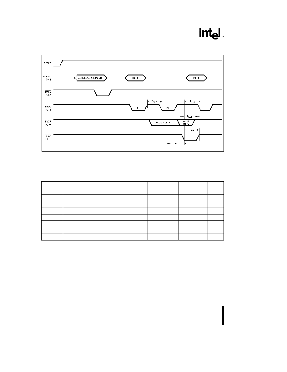
T
AVLL
Address Setup Time
0
T
OSC
T
LLAX
Address Hold Time
100
T
OSC
T
DVPL
Data Setup Time
0
T
OSC
T
PLDX
Data Hold Time
400
T
OSC
T
LLLH
PALE Pulse Width
50
T
OSC
T
PLPH
PROG Pulse Width
(2)
50
T
OSC
T
LHPL
PALE High to PROG Low
220
T
OSC
T
PHLL
PROG High to next PALE Low
220
T
OSC
T
PHDX
Word Dump Hold Time
50
T
OSC
T
PHPL
PROG High to next PROG Low
220
T
OSC
T
LHPL
PALE High to PROG Low
220
T
OSC
T
PLDV
PROG Low to Word Dump Valid
50
T
OSC
T
SHLL
RESET High to First PALE Low
1100
T
OSC
T
PHIL
PROG High to AINC Low
0
T
OSC
T
ILIH
AINC Pulse Width
240
T
OSC
T
ILVH
PVER Hold after AINC Low
50
T
OSC
T
ILPL
AINC Low to PROG Low
170
T
OSC
T
PHVL
PROG High to PVER Valid
220
T
OSC
NOTES
1 Run-time programming is done with Fosc
e
6 0 MHz to 10 0 MHz V
CC
V
PD
V
REF
e
5V
g
0 5V T
C
e
25 C
g
5 C and
V
PP
e
12 5V
g
0 25V For run-time programming over a full operating range contact factory
2 Programming specifications are not tested but guaranteed by design
3 This specification is for the word dump mode For programming pulses use 300 Tosc
a
100 ms
DC EPROM PROGRAMMING CHARACTERISTICS
Symbol
Parameter
Min
Max
Units
I
PP
V
PP
Programming Supply Current
200
mA
NOTE
V
PP
must be within 1V of V
CC
while V
CC
k
4 5V V
PP
must not have a low impedance path to ground or V
SS
while V
CC
l
4 5V
26
26
87C196KT 87C196KS
EPROM PROGRAMMING WAVEFORMS
SLAVE PROGRAMMING MODE DATA PROGRAM MODE WITH SINGLE PROGRAM PULSE
270999 � 19
SLAVE PROGRAMMING MODE IN WORD DUMP OR DATA VERIFY MODE WITH AUTO INCREMENT
270999 � 20
27
27
87C196KT 87C196KS
SLAVE PROGRAMMING MODE TIMING IN DATA PROGRAM MODE WITH REPEATED PROG PULSE
AND AUTO INCREMENT
270999 � 21
AC CHARACTERISTICS
SERIAL PORT-SHIFT REGISTER MODE
SERIAL PORT TIMING
SHIFTING REGISTER MODE
Test Conditions T
A
e b
40 C to a125 C V
CC
e
5 0V
g
10% V
SS
e
0 0V Load Capacitance e pF
Symbol
Parameter
Min
Max
Units
T
XLXL
Serial Port Clock Period
8 T
OSC
ns
T
XLXH
Serial Port Clock Falling Edge to Rising Edge
4 T
OSC
b
50
T
OSC
a
50
ns
T
QVXH
Output Data Setup to Clock Rising Edge
3 T
OSC
ns
T
XHQX
Output Data Hold after Clock Rising Edge
2 T
OSC
b
50
ns
T
XHQV
Next Output Data Valid after Clock Rising Edge
2 T
OSC
a
50
ns
T
DVXH
Input Data Setup to Clock Rising Edge
2 T
OSC
a
200
ns
T
XHDX
(8)
Input Data Hold after Clock Rising Edge
0
ns
T
XHQZ
(8)
Last Clock Rising to Output Float
5 T
OSC
ns
NOTE
8 Parameters not tested
28
28
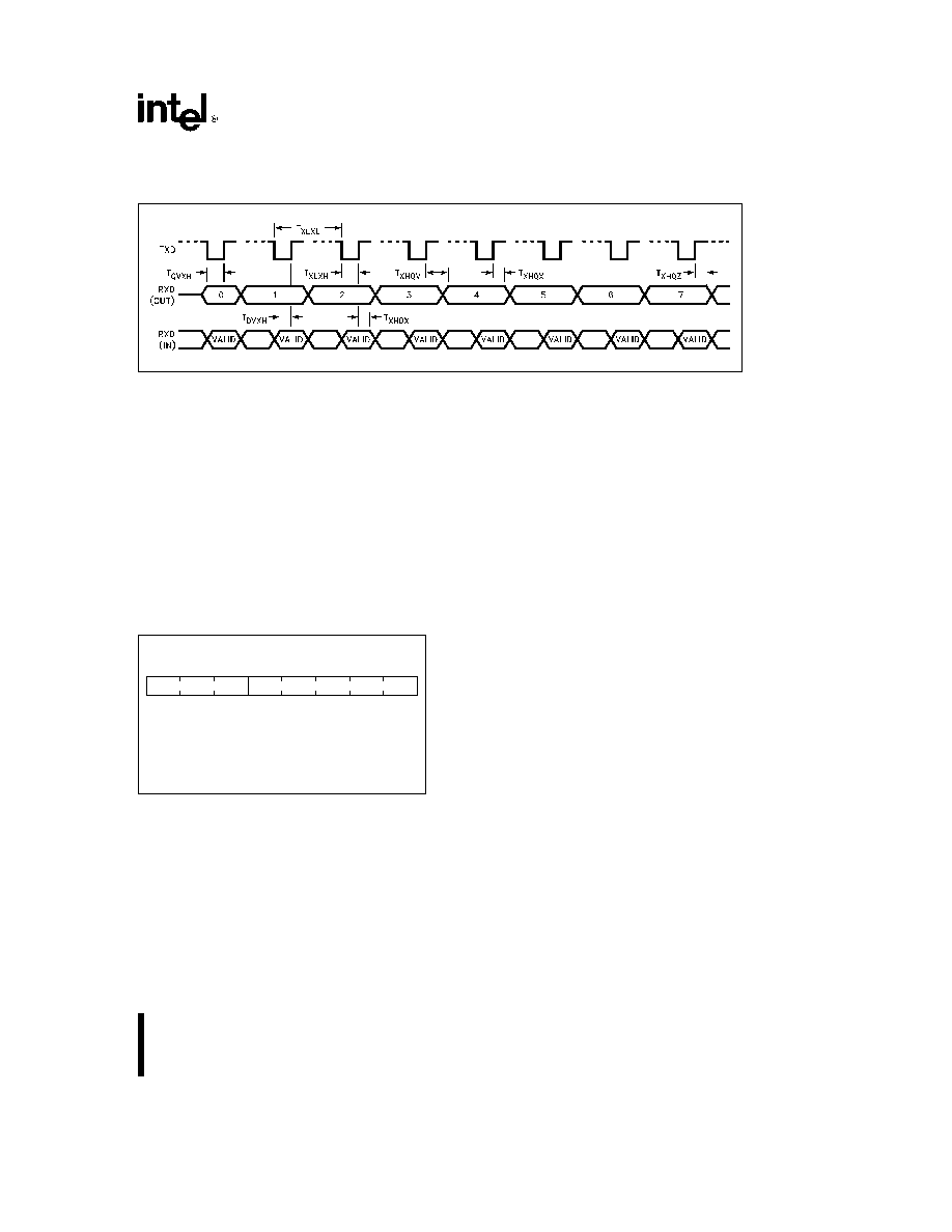
87C196KT 87C196KS
WAVEFORM
SERIAL PORT
SHIFT REGISTER MODE
SERIAL PORT WAVEFORM
SHIFT REGISTER MODE
270999 � 22
A TO D CHARACTERISTICS
The sample and conversion time of the A D convert-
er in the 8-bit or 10-bit modes is programmed by
loading a byte into the AD
TIME Special Function
Register This allows optimizing the A D operation
for specific applications The AD
TIME register is
functional for all possible values but the accuracy of
the A D converter is only guaranteed for the times
specified in the operating conditions table
The value loaded into AD
TIME bits 5 6 7 deter-
mines the sample time SAMP The value loaded
into AD
TIME bits 0 1 2 3 and 4 determines the
bit conversion time CONV These bits as well as
the equation for calculating the total conversion
time T are shown in the following table
AD
TIME
1FAFH Byte
7
6
5
4
3
2
1
0
Sample Time
Bit Conversion Time
(SAMP)
(CONV)
4n a 1 state times
n a1 state times
n e 1 to 7
n e 2 to 31
Equation
T
e
(SAMP)
a
Bx (CONV)
a
2 5
T
e
total conversion time (states)
B
e
number of bits conversion (8 or 10)
n
e
programmed register value
The converter is ratiometric so absolute accuracy is
dependent on the accuracy and stability of V
REF
V
REF
must be close to V
CC
since it supplies both the
resistor ladder and the analog portion of the convert-
er and input port pins There is also an AD
TEST
SFR that allows for conversion on ANGND and
V
REF
as well as adjusting the zero offset The abso-
lute error listed is without doing any adjustments
A D CONVERTER SPECIFICATION
The specifications given assume adherence to the
operating conditions section of this data sheet Test-
ing is performed with V
REF
e
5 12V and 16 MHz
operating frequency After a conversion is started
the device is placed in IDLE mode until the conver-
sion is complete
29
29

87C196KT 87C196KS
10-BIT MODE A D OPERATING CONDITIONS
Symbol
Description
Min
Max
Units
T
A
Ambient Temperature
b
40
a
125
C
V
CC
Digital Supply Voltage
4 50
5 50
V
V
REF
Analog Supply Voltage
4 50
5 50
V
(1)
T
SAM
Sample Time
2 0
m
s
(2)
T
CONV
Conversion Time
15
18
m
s
(2)
F
OSC
Oscillator Frequency
4 0
16 0
MHz
NOTES
1 V
REF
must be within 0 5V of V
CC
2 The value of AD
TIME is selected to meet these specifications
10-BIT MODE A D CHARACTERISTICS
(Using Above Operating Conditions)
(6)
Parameter
Typ
(1)
Min
Max
Units
Resolution
1024
1024
Level
10
10
Bits
Absolute Error
0
g
3 0
LSBs
Full Scale Error
0 25
g
0 5
LSBs
Zero Offset Error
0 25
g
0 5
LSBs
Non-Linearity
1 0
g
2 0
g
3 0
LSBs
Differential Non-Linearity
b
0 75
a
0 75
LSBs
Channel-to-Channel Matching
g
0 1
0
g
1 0
LSBs
Repeatability
g
0 25
0
LSBs
(1)
Temperature Coefficients
Offset
0 009
LSB C
(1)
Full Scale
0 009
LSB C
(1)
Differential Non-Linearity
0 009
LSB C
(1)
Off Isolation
b
60
dB
(1 2 3)
Feedthrough
b
60
dB
(1 2)
V
CC
Power Supply Rejection
b
60
dB
(1 2)
Input Resistance
750
1 2K
X
(4)
DC Input Leakage
g
1 0
0
g
1 5
m
A
Sampling Capacitor
3 0
pF
An ``LSB'' as used here has a value of approximately 5 mV
NOTES
1 These values are expected for most parts at 25 C but are not tested or guaranteed
2 DC to 100 KHz
3 Multiplexer break-before-make is guaranteed
4 Resistance from device pin through internal MUX to sample capacitor
5 All conversions performed with processor in IDLE mode
30
30

87C196KT 87C196KS
8-BIT MODE A D OPERATING CONDITIONS
Symbol
Description
Min
Max
Units
T
A
Ambient Temperature
b
40
a
125
C
V
CC
Digital Supply Voltage
4 50
5 50
V
V
REF
Analog Supply Voltage
4 50
5 50
V
(1)
T
SAM
Sample Time
2 0
m
s
(2)
T
CONV
Conversion Time
12
15
m
s
(2)
F
OSC
Oscillator Frequency
4 0
16 0
MHz
NOTES
1 V
REF
must be within 0 5V of V
CC
2 The value of AD
TIME is selected to meet these specifications
8-BIT MODE A D CHARACTERISTICS
(Using Above Operating Conditions)
(6)
Parameter
Typ
(1)
Min
Max
Units
Resolution
256
256
Level
8
8
Bits
Absolute Error
0
g
1 0
LSBs
Full Scale Error
g
0 5
LSBs
Zero Offset Error
g
0 5
LSBs
Non-Linearity
0
g
1 0
LSBs
Differential Non-Linearity
b
0 5
a
0 5
LSBs
Channel-to-Channel Matching
0
g
1 0
LSBs
Repeatability
g
0 25
0
LSBs
(1)
Temperature Coefficients
Offset
0 003
LSB C
(1)
Full Scale
0 003
LSB C
(1)
Differential Non-Linearity
0 003
LSB C
(1)
Off Isolation
b
60
dB
(1 2 3)
Feedthrough
b
60
dB
(1 2)
V
CC
Power Supply Rejection
b
60
dB
(1 2)
Input Resistance
750
1 2K
X
(4)
DC Input Leakage
g
1 0
0
g
1 5
m
A
Voltage on Analog Input Pin
ANGND b 0 5
V
REF
a
0 5
V
(5)
Sampling Capacitor
3 0
pF
An ``LSB'' as used here has a value of approximately 20 mV
NOTES
1 These values are expected for most parts at 25 C but are not tested or guaranteed
2 DC to 100 KHz
3 Multiplexer break-before-make is guaranteed
4 Resistance from device pin through internal MUX to sample capacitor
5 Applying voltage beyond these specifications will degrade the accuracy of other channels being converted
6 All conversions performed with processor in IDLE mode
31
31

87C196KT 87C196KS
87C196KT KS ERRATA
The following is a list of all known functional devia-
tions for 87C196KT KS devices B-step and later
devices can be identified by a special mark following
the eight digit FPO number on the top of the pack-
age For C-step devices this mark is a ``C''
1 HOLD OR READY DURING DIVIDE (A-step)
There is a bug in the DIV and DIVB (signed di-
vide) instructions such that if the following 2 con-
ditions are met there may be an error of 1 in the
quotient
a) HOLD or READY is asserted during the first
state of execution of the DIV and DIVB in-
struction
b) HOLD or READY duration is 16 state times for
the DIVB or 24 state times for a DIV instruc-
tion
2 P2 7 (CLKOUT) (A-step)
Port 2 7 (CLKOUT) does not operate in open
drain mode
3 P2
REG 7 AND P6
REG 4 THROUGH P6
REG 7 CLEARED (A-step)
P2
REG 7 is cleared when P2
SSEL 7 bit is
changed from a 1 to a 0 (special function to
LSIO) P6
Reg 4 � 7 is cleared when the corre-
sponding P6
SSEL 4 � 7 is changed from a 1 to
a 0
4 INDIRECT SHIFT INSTRUCTION (A-step)
The upper three bits of the byte register holding
the shift count are not masked completely If the
shift count register has the value 32 x n where n
e
1 3 5 or 7 the operand wil be shifted 32
times The above condition results in NO shift
taking place
5 INTERNAL RAM POWERDOWN LEAKAGE
(A-step)
If an invalid address is applied to the internal
RAM during power-down the address lines float
This can cause increased current consumption
during power-down To insure a valid address on
the internal RAM execute the idle power-down
instruction from internal RAM
6 INST PIN (A-step)
On A-step devices the INST pin is pulled medium
low for approx 200 ns after RESET and then
pulled weakly
HIGH
until P5SSEL is written to
This is corrected on B-step devices where the
INST pin is pulled medium low for approx 200 ns
after RESET and is then pulled weakly
LOW
until
P5SSEL is written to
7 REGISTER
RAM
OVERWRITE
(A-step
B-step)
If a write is performed to a byte word location
within the SFR range of 1F60h to 1FFFh the
data to be written is also written to a correspond-
ding location located within the REGISTER RAM
space 360h to 3FFh To determine the address
of the REGISTER RAM location that is overwrit-
ten an offset of 1C00h can be subtracted from
the byte word addressed in the SFR range
8 BUS TIMING MODES 1 AND 2 (A-step B-step)
Bus timing modes 1 and 2 are not featured or
specified on A-step and B-step parts On C-step
parts Mode 1 is selected by setting bits MSEL1
e
0 and MSEL0 e 1 in the CCB1 register
Mode 2 is similarly selected by setting MSEL1 e
1 and MSEL0 e 0
Timings are altered by
Mode 1 and Mode 2 as follows (for actual values
see the Bus Mode 1 and Bus Mode 2 AC Charac-
teristics in this data sheet)
Mode 1 RD WR advanced 1 T
OSC
ALE advanced 0 5 T
OSC
ALE pulse width remains 1 T
OSC
Mode 2 RD WR advanced 1 T
OSC
ALE advanced 0 5 T
OSC
ALE pulse width remains 1 T
OSC
Address advanced 0 5 T
OSC
9 V
OH2
(A-step b-step)
A- and B-step parts are capable of V
OH2
e
V
CC
b
1V with I
OH
e
b
6 mA C-step devices meet
the target values of V
OH2
e
V
CC
b
1V with I
OH
e b
15 mA
10 CLKOUT DURING RESET (A-step
B-step
C-step)
For
all
steppings
of
the
87C196KT
the
CLKOUT function during RESET (P2 7) differs
from the 87C196KR C-step During RESET on
the 87C196KT CLKOUT does not toggle and
remains in the high state During RESET on the
87C196KR C-step CLKOUT countinues to tog-
gle
32
32

87C196KT 87C196KS
87C196KT KS DESIGN CONSIDERATIONS
1 EPA TIMER RESET WRITE CONFLICT
If the user writes to the EPA timer at the same
time that the timer is reset it is indeterminate
which will take precedence Users should not
write to a timer if using EPA signals to reset it
2 VALID TIME MATCHES
The timer must increment decrement to the
compare value for a match to occur A match
does not occur if the timer is loaded with a value
equal to an EPA compare value Matches also do
not occur if a timer is reset and 0 is the EPA
compare value
3 P6
PIN 4- 7 NOT UPDATED IMMEDIATELY
Values written to P6
REG are temporarily held
in a buffer If P6
MODE is cleared the buffer is
loaded into P6
REG x If P6
MODE is set the
value stays in the buffer and is loaded into
P6
REG x when P6
MODE x is cleared Since
reading P6
REG returns the current value in
P6
REG and not the buffer
changes to
P6
REG
cannot
be
read
until unless
P6
MODE x is cleared
4 WRITE CYCLE DURING RESET
If RESET occurs during a write cycle the con-
tents of the external memory device may be cor-
rupted
5 INDIRECT SHIFT INSTRUCTION
The upper 3 bits of the byte register holding the
shift count are not masked completely If the shift
count register has the value 32
c
n where
n e 1 3 5 or 7 the operand will be shifted 32
times This should have resulted in no shift taking
place
6 PORT 4 ADDRESS BEHAVIOR
For bus timing Modes 1 and 2 specified only on
the 87C196KT KS C-step Port 4 does not retain
the address during the data portion of the bus
cycle
Designs using an 8-bit external memory
system in bus Mode 1 or Mode 2 require an ex-
ternal latch on Port 4 to retain the address during
the data portion of the bus cycle
Designs using
an 8-bit external memory system in the KR or
KR a 1 Wait
bus timing modes do not require an
external latch
Designs using 16-bit external
memory systems require an external latch on
both Port 3 and Port 4 in all bus timing modes
33
33

87C196KT 87C196KS
DATA SHEET REVISION HISTORY
This is the -007 revision of the 8XC196KT KS Data Sheet The following differences exist between the -006
revision and the -007 revision
1 V
OL3
estimate added
2 ``Voltage on Analog Input Pin'' removed
Parameter covered by Note 1 V
REF
must be within 0 5V of V
CC
3 The
Data Sheet Revision History
was updated to reflect changes made for this version of the datasheet
(-007)
34
34