 | –≠–ª–µ–∫—Ç—Ä–æ–Ω–Ω—ã–π –∫–æ–º–ø–æ–Ω–µ–Ω—Ç: 87C51FA-1 | –°–∫–∞—á–∞—Ç—å:  PDF PDF  ZIP ZIP |

Other brands and names are the property of their respective owners
Information in this document is provided in connection with Intel products Intel assumes no liability whatsoever including infringement of any patent or
copyright for sale and use of Intel products except as provided in Intel's Terms and Conditions of Sale for such products Intel retains the right to make
changes to these specifications at any time without notice Microcomputer Products may have minor variations to this specification known as errata
September 1993
COPYRIGHT
INTEL CORPORATION 1995
Order Number 270961-003
87C51FA 87C51FB 87C51FC 87C51FC-20
CHMOS SINGLE-CHIP 8-BIT MICROCONTROLLER
Automotive
Y
FX Core Architecture Device
Y
Extended Automotive Temperature
Range (
b
40 C to
a
125 C Ambient)
Y
Available in 12 MHz 16 MHz and
20 MHz Versions
Y
High Performance CHMOS EPROM
Y
Three 16-Bit Timer Counters
Timer 2 (Up Down Counter)
Y
Programmable Counter Array with
High Speed Output
Compare Capture
Pulse Width Modulator
Watchdog Timer Capabilities
Y
One-to-Three Level Program Lock
System on EPROM
Y
8K On-Chip User Programmable
EPROM in 87C51FA
Y
16K On-Chip User Programmable
EPROM in 87C51FB
Y
32K On-Chip User Programmable
EPROM in 87C51FC
Y
256 Bytes of On-Chip Data RAM
Y
Quick Pulse Programming Algorithm
Y
Boolean Processor
Y
32 Programmable I O Lines
Y
7 Interrupt Sources
Y
Four Level Interrupt Priority
Y
Programmable Serial Channel with
Framing Error Detection
Automatic Address Recognition
Y
TTL and CMOS Compatible Logic
Levels
Y
64K External Program Memory Space
Y
64K External Data Memory Space
Y
MCS -51 Fully Compatible Instruction
Set
Y
Power Saving Idle and Power Down
Modes
Y
ONCE (On-Circuit Emulation) Mode
Y
RFI Reduction Mode
Y
Available in PLCC and PDIP Packages
MEMORY ORGANIZATION
PROGRAM MEMORY Up to 8 Kbytes of the program memory can reside in the 87C51FA On-Chip EPROM
Up to 16 Kbytes of the program memory can reside in the 87C51FB on-chip EPROM Up to 32 Kbytes of the
program memory can reside in the 87C51FC on-chip EPROM In addition the device can address up to 64K of
program memory external to the chip
DATA MEMORY This microcontroller has a 256 x 8 on-chip RAM In addition it can address up to 64 Kbytes of
external data memory
The Intel 87C51FA 87C51FB 87C51FC is a single-chip control-oriented microcontroller which is fabricated on
Intel's reliable CHMOS EPROM technology Being a member of the MCS-51 family the 87C51FB 87C51FC
uses the same powerful instruction set has the same architecture and is pin-for-pin compatible with the
existing MCS-51 family of products The 87C51FA is an enhanced version of the 87C51 The 87C51FB is an
enhanced version of the 87C51FA The 87C51FC is an enhanced version of the 87C51FB With 8 Kbytes of
program memory in the 87C51FA and 16 Kbytes of program memory in the 87C51FB and 32 Kbytes of
program memory in the 87C51FC it is an even more powerful microcontroller for applications that require
Pulse Width Modulation High Speed I O and up down counting capabilities such as brake and traction
control
For the remainder of this document the 87F51FA 87C51FB and 87C51FC will be referred to as the
87C51FA FB FC
AUTOMOTIVE 87C51FA FB FC FC-20
270961 ≠ 1
Figure 1 87C51FB FC Block Diagram
87C51FA FB FC PRODUCT OPTIONS
Intel's extended and automotive temperature range
products are designed to meet the needs of those
applications whose operating requirements exceed
commercial standards
With the commercial standard temperature range
operational characteristics are guaranteed over the
temperature range of 0 C to 70 C ambient With the
extended temperature range option
operational
characteristics are guaranteed over the temperature
2
AUTOMOTIVE 87C51FA FB FC FC-20
range of b40 C to a85 C ambient For the automo-
tive temperature range option operational charac-
teristics are guaranteed over the temperature range
of b40 C to a125 C ambient The automotive ex-
tended and commercial temperature versions of the
MCS-51 product families are available with or with-
out burn-in options
As shown in Figure 2 temperature burn-in and
package options are identified by a one- or two-letter
prefix to the part number
PIN DESCRIPTIONS
V
CC
Supply voltage
V
SS
Circuit ground
V
SS1
Secondary ground (in PLCC only) Provided to
reduce ground bounce and improve power supply
by-passing
NOTE
This pin is NOT a substitute for V
SS
pin (pin 22)
Port 0
Port 0 is an 8-bit open drain bidirectional
I O port As an output port each pin can sink several
LS TTL inputs Port 0 pins that have 1's written to
them float and in that state can be used as high-im-
pedance inputs
270961 ≠ 2
Example
AN87C51FA FB FC indicates an automotive temperature range version of the 87C51FA FB FC in a PLCC package
with 16 Kbyte 32 Kbyte EPROM program memory
Figure 2 Package Options
Table 1 Temperature Options
Temperature
Temperature
Operating
Burn-In
Classification
Designation
Temperature
Options
C Ambient
Extended
T
b
40 to a85
Standard
L
b
40 to a85
Extended
Automotive
A
b
40 to a125
Standard
B
b
40 to a125
Extended
3
AUTOMOTIVE 87C51FA FB FC FC-20
Port 0 is also the multiplexed low-order address and
data bus during accesses to external Program and
Data Memory In this application it uses strong inter-
nal pullups when emitting 1's and can source and
sink several LS TTL inputs
Port 0 also receives the code bytes during EPROM
programming and outputs the code bytes during
program verification External pullup resistors are re-
quired during program verification
Port 1
Port 1 is an 8-bit bidirectional I O port with
internal pullups The Port 1 output buffers can drive
LS TTL inputs Port 1 pins that have 1's written to
them are pulled high by the internal pullups and in
that state can be used as inputs As inputs Port 1
pins that are externally pulled low will source current
(I
IL
on the data sheet) because of the internal pull-
ups
In addition Port 1 serves the functions of the follow-
ing special features of the 87C51FB FC
Port Pin
Alternate Function
P1 0
T2 (External Count Input to
Timer Counter 2)
P1 1
T2EX (Timer Counter 2 Capture
Reload Trigger and Direction Control)
P1 2
ECI (External Count Input to the PCA)
P1 3
CEX0 (External I O for Compare
Capture Module 0)
P1 4
CEX1 (External I O for Compare
Capture Module 1)
P1 5
CEX2 (External I O for Compare
Capture Module 2)
P1 6
CEX3 (External I O for Compare
Capture Module 3)
P1 7
CEX4 (External I O for Compare
Capture Module 4)
Port 1 receives the low-order address bytes during
EPROM programming and verifying
Port 2
Port 2 is an 8-bit bidirectional I O port with
internal pullups The Port 2 output buffers can drive
LS TTL inputs Port 2 pins that have 1's written to
them are pulled high by the internal pullups and in
that state can be used as inputs As inputs Port 2
pins that are externally pulled low will source current
(I
IL
on the data sheet) because of the internal pull-
ups
PACKAGES
Part
Prefix
Package Type
87C51FA FB FC
P
40-Pin Plastic DIP
N
44-Pin PLCC
DIP
270961 ≠ 3
PAD (PLCC)
270961 ≠ 4
EPROM only
Do not connect reserved pins
Diagrams are for pin reference only Package sizes are
not to scale
Figure 3 Pin Connections (Top View)
4

AUTOMOTIVE 87C51FA FB FC FC-20
Port 2 emits the high-order address byte during
fetches from external Program Memory and during
accesses to external Data Memory that use 16-bit
addresses (MOVX
DPTR) In this application it
uses strong internal pullups when emitting 1's Dur-
ing accesses to external Data Memory that use 8-bit
addresses (MOVX
Ri) Port 2 emits the contents
of the P2 Special Function Register
Some Port 2 pins receive the high-order address bits
during EPROM programming and program verifica-
tion
Port 3
Port 3 is an 8-bit bidirectional I O port with
internal pullups The Port 3 output buffers can drive
LS TTL inputs Port 3 pins that have 1's written to
them are pulled high by the internal pullups and in
that state can be used as inputs As inputs Port 3
pins that are externally pulled low will source current
(I
IL
on the data sheet) because of the pullups
Port 3 also serves the functions of various special
features of the MCS-51 Family as listed below
Port Pin
Alternate Function
P3 0
RXD (serial input port)
P3 1
TXD (serial output port)
P3 2
INT0 (external interrupt 0)
P3 3
INT1 (external interrupt 1)
P3 4
T0 (Timer 0 external input)
P3 5
T1 (Timer 1 external input)
P3 6
WR (external data memory write strobe)
P3 7
RD (external data memory read strobe)
RST
Reset input A high on this pin for two machine
cycles while the oscillator is running resets the de-
vice The port pins will be driven to their reset condi-
tion when a minimum V
IH1
is applied whether the
oscillator is running or not An internal pulldown re-
sistor permits a power-on reset with only a capacitor
connected to V
CC
ALE PROG
Address Latch Enable output pulse for
latching the low byte of the address during accesses
to external memory This pin (ALE PROG) is also
the program pulse input during EPROM program-
ming for the 87C51FA FB FC
In normal operation ALE is emitted at a constant
rate of
the oscillator frequency and may be used
for external timing or clocking purposes Note how-
ever that one ALE pulse is skipped during each ac-
cess to external Data Memory
Throughout the remainder of this data sheet ALE
will refer to the signal coming out of the ALE PROG
pin and the pin will be referred to as the ALE PROG
pin
PSEN
Program Store Enable is the read strobe to
external Program Memory
When the 87C51FA FB FC is executing code from
external Program Memory PSEN is activated twice
each machine cycle except that two PSEN activa-
tions are skipped during each access to external
Data Memory
EA V
PP
External Access enable
EA must be
strapped to V
SS
in order to enable the device to
fetch code from external Program Memory locations
0000H to 0FFFFH Note however that if either of
the Program Lock bits are programmed EA will be
internally latched on reset
EA should be strapped to V
CC
for internal program
executions
This pin also receives the programming supply volt-
age (V
PP
) during EPROM programming
XTAL1
Input to the inverting oscillator amplifier
XTAL2
Output from the inverting oscillator amplifier
OSCILLATOR CHARACTERISTICS
XTAL1 and XTAL2 are the input and output respec-
tively of an inverting amplifier which can be config-
ured for use as an on-chip oscillator as shown in
Figure 4 Either a quartz crystal or ceramic resonator
may be used More detailed information concerning
the use of the on-chip oscillator is available in Appli-
cation Note AP-155 ``Oscillators for Microcontrol-
lers'' and in Application Note AP-486
``Oscillator
Design for Microcontrollers''
5
AUTOMOTIVE 87C51FA FB FC FC-20
To drive the device from an external clock source
XTAL1 should be driven while XTAL2 floats as
shown in Figure 5 There are no requirements on the
duty cycle of the external clock signal since the in-
put to the internal clocking circuitry is through a di-
vide-by-two flip-flop but minimum and maximum
high and low times specified on the data sheet must
be observed
An external oscillator may encounter as much as
100 pF load at XTAL1 when it starts up This is due
to interaction between the amplifier and its feedback
capacitance Once the external signal meets V
IL
and
V
IH
specifications the capacitance will not exceed
20 pF
270961 ≠ 5
C1 C2
e
30 pF
g
10 pF for Crystals
For Ceramic Resonators contact resonator manufac-
turer
Figure 4 Oscillator Connections
270961 ≠ 6
Figure 5 External Clock Drive Configuration
IDLE MODE
The user's software can invoke the Idle Mode When
the microcontroller is in this mode power consump-
tion is reduced The Special Function Registers and
the onboard RAM retain their values during Idle but
the processor stops executing instructions
Idle
Mode will be exited if the chip is reset or if an en-
abled interrupt occurs The PCA timer counter can
optionally be left running or paused during Idle
Mode
POWER DOWN MODE
To save even more power a Power Down mode can
be invoked by software In this mode the oscillator
is stopped and the instruction that invoked Power
Down is the last instruction executed The on-chip
RAM and Special Function Registers retain their val-
ues until the Power Down mode is terminated
On the 87C51FA FB FC either a hardware reset or
external interrupt can cause an exit from Power
Down Reset redefines all the SFRs but does not
change the on-chip RAM An external interrupt al-
lows both the SFRs and the on-chip RAM to retain
their values
To properly terminate Power Down the reset or ex-
ternal interrupt should not be executed before V
CC
is
restored to its normal operating level and must be
held active long enough for the oscillator to restart
and stabilize (normally less than 10 ms)
With an external interrupt INT0 or INT1 must be en-
abled and configured as level-sensitive Holding the
pin low restarts the oscillator (the oscillator must be
allowed time to stabilize after start up before this pin
is released high) but bringing the pin back high com-
pletes the exit Once the interrupt is serviced the
next instruction to be executed after RETI will be the
one following the instruction that put the device into
Power Down
6

AUTOMOTIVE 87C51FA FB FC FC-20
DESIGN CONSIDERATION
When the Idle mode is terminated by a hardware
reset the device normally resumes program execu-
tion from where it left off up to two machine cycles
before the internal reset algorithm takes control On-
chip hardware inhibits access to internal RAM in this
event but access to the port pins is not inhibited To
eliminate the possibility of an unexpected write when
Idle is terminated by reset the instruction following
the one that invokes Idle should not be one that
writes to a port pin or to external memory
ONCE MODE
The ONCE (``On-Circuit Emulation'') Mode facilitates
testing
and
debugging
of
systems
using
the
87C51FA FB FC without removing it from the cir-
cuit The ONCE Mode is invoked by
1 Pull ALE low while the device is in reset and
PSEN is high
2 Hold ALE low as RST is deactivated
While the device is in ONCE Mode the Port 0 pins
float and the other port pins and ALE and PSEN are
weakly pulled high The oscillator circuit remains ac-
tive While the 87C51FA FB FC is in this mode an
emulator or test CPU can be used to drive the circuit
Normal operation is restored when a normal reset is
applied
RFI REDUCTION MODE
The RFI reduction feature can be used only if exter-
nal program memory is not required since this mode
disables the ALE pin during instruction code fetches
By writing a logical one to the LSB of the Auxiliary
Register (address 08EH) the ALE is disabled for in-
struction code fetches and the output is weakly held
high When a logical zero is written the ALE pin is
enabled allowing it to generate the Address Latch
Enable signal This bit is cleared by reset Once dis-
abled ALE remains disabled until it is reset by soft-
ware or until a hardware reset occurs
Table 2 Status of the External Pins during Idle and Power Down
Mode
Program
ALE
PSEN
PORT0
PORT1
PORT2
PORT3
Memory
Idle
Internal
1
1
Data
Data
Data
Data
Idle
External
1
1
Float
Data
Address
Data
Power Down
Internal
0
0
Data
Data
Data
Data
Power Down
External
0
0
Float
Data
Data
Data
NOTE
For more detailed information on the reduced power modes refer to current Embedded Applications Handbook and Applica-
tion Note AP-252 ``Designing with the 80C51BH ''
7

AUTOMOTIVE 87C51FA FB FC FC-20
ABSOLUTE MAXIMUM RATINGS
Ambient Temperature Under Bias b40 C to a125 C
Storage Temperature
b
65 C to a150 C
Voltage on EA V
PP
Pin to V
SS
0V to a13 0V
Voltage on Any Other Pin to V
SS
b
0 5V to a6 5V
I
OL
Per I O Pin
15 mA
Power Dissipation
1 5W
(Based on package heat transfer limitations not
device power consumption)
Typical Junction Temperature
a
135 C
(Based on ambient temperature at a125 C)
Typical Thermal Resistance Junction-to-Ambient
(i
JA
)
PDIP
45 C W
PLCC
46 C W
NOTICE This data sheet contains information on
products in the sampling and initial production phases
of development The specifications are subject to
change without notice Verify with your local Intel
Sales office that you have the latest data sheet be-
fore finalizing a design
WARNING Stressing the device beyond the ``Absolute
Maximum Ratings'' may cause permanent damage
These are stress ratings only Operation beyond the
``Operating Conditions'' is not recommended and ex-
tended exposure beyond the ``Operating Conditions''
may affect device reliability
ADVANCED INFORMATION
CONTACT INTEL FOR DESIGN-IN INFORMATION
DC CHARACTERISTICS
(T
A
e b
40 C to a125 C V
CC
e
5V
g
20% V
SS
e
0V)
Symbol
Parameter
Min
Typ
Max
Unit
Test Conditions
(Note 4)
V
IL
Input Low Voltage
b
0 5
0 2 V
CC
b
0 1
V
V
IL1
Input Low Voltage EA
0
0 2 V
CC
b
0 3
V
V
IH
Input High Voltage
0 2 V
CC
a
0 9
V
CC
a
0 5
V
(Except XTAL1 RST EA)
V
IH1
Input High Voltage (XTAL1 RST)
0 7 V
CC
V
CC
a
0 5
V
V
OL
Output Low Voltage (Note 5)
0 3
V
I
OL
e
100 mA (Note 1)
(Ports 1 2 and 3)
0 45
V
I
OL
e
1 6 mA (Note 1)
1 0
V
I
OL
e
3 5 mA (Note 1)
V
OL1
Output Low Voltage (Note 5)
0 3
V
I
OL
e
200 mA (Note 1)
(Port 0 ALE PSEN)
0 45
V
I
OL
e
3 2 mA (Note 1)
1 0
V
I
OL
e
7 0 mA (Note 1)
V
OH
Output High Voltage
V
CC
b
0 3
V
I
OH
e b
10 mA
(Ports 1 2 and 3)
V
CC
b
0 7
V
I
OH
e b
30 mA
V
CC
b
1 5
V
I
OH
e b
60 mA
V
OH1
Output High Voltage
V
CC
b
0 3
V
I
OH
e b
200 mA
(Port 0 in External Bus Mode
V
CC
b
0 7
V
I
OH
e b
3 2 mA
ALE PSEN)
V
CC
b
1 5
V
I
OH
e b
7 0 mA
I
IL
Logical 0 Input Current
b
75
m
A V
IN
e
0 45V
(Ports 1 2 and 3)
I
LI1
Input Leakage Current (Port 0)
g
10
m
A 0 45V
k
V
IN
k
V
CC
I
TL
Logical 1 to 0 Transition Current
b
750
m
A V
IN
e
2V
(Ports 1 2 and 3)
RRST
RST Pulldown Resistor
40
225
KX
CIO
Pin Capacitance
10
pF
1 MHz 25 C
I
CC
Power Supply Current
(Note 3)
Running at 16 20 MHz (Figure 6)
26 28
35 40
mA
Idle Mode at 16 20 MHz (Figure 6)
5
12 14
mA
Power Down Mode
15
100
m
A
8
AUTOMOTIVE 87C51FA FB FC FC-20
NOTES
1 Capacitive loading on Ports 0 and 2 may cause noise pulses above 0 4V to be superimposed on the V
OL
s of ALE and
Ports 1 2 and 3 The noise is due to external bus capacitance discharging into the Port 0 and Port 2 pins when these pins
change from 1 to 0 In applications where capacitive loading exceeds 100 pF the noise pulses on these signals may exceed
0 8V It may be desirable to qualify ALE or other signals with Schmitt triggers or CMOS-level input logic
2 Capacitive loading on Ports 0 and 2 cause the V
OH
on ALE and PSEN to drop below the 0 9 V
CC
specification when the
address lines are stabilizing
3 See Figures 6 ≠ 9 for test conditions Minimum V
CC
for Power Down is 2V
4 Typicals are based on limited number of samples and are not guaranteed The values listed are at room temperature and
5V
5 Under steady state (non-transient) conditions I
OL
must be externally limited as follows
Maximum I
OL
per port pin
10mA
Maximum I
OL
per 8-bit port
Port 0
26 mA
Ports 1 2 and 3
15 mA
Maximum total I
OL
for all output pins
71 mA
If I
OL
exceeds the test condition V
OL
may exceed the related specification Pins are not guaranteed to sink current greater
than the listed test conditions
270961 ≠ 7
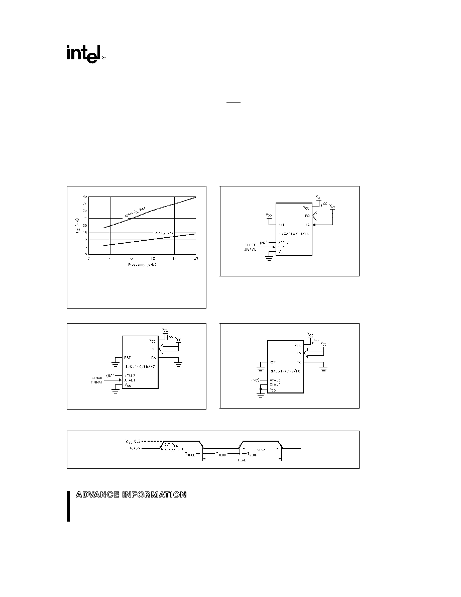
I
CC
Max at other frequencies is given by
Active Mode
I
CC
Max e (1 25
c
Osc Freq) a 15
Idle Mode
I
CC
Max e (0 5
c
Osc Freq) a 4
Where Osc Freq is in MHz I
CC
is in mA
Figure 6 I
CC
vs Frequency
All other pins disconnected
270961 ≠ 8
TCLCH e TCHCL e 5 ns
Figure 7 I
CC
Test Condition Active Mode
All other pins disconnected
270961 ≠ 9
TCLCH e TCHCL e 5 ns
Figure 8 I
CC
Test Condition Idle Mode
All other pins disconnected
270961 ≠ 10
Figure 9 I
CC
Test Condition Power Down Mode
V
CC
e
2 0V to 5 5V
270961 ≠ 11
Figure 10 Clock Signal Waveform for I
CC
Tests in Active and Idle Modes TCLCH e TCHCL e 5 ns
9
AUTOMOTIVE 87C51FA FB FC FC-20
EXPLANATION OF THE AC SYMBOLS
Each timing symbol has 5 characters The first char-
acter is always a `T' (stands for time) The other
characters depending on their positions stand for
the name of a signal or the logical status of that
signal The following is a list of all the characters and
what they stand for
A Address
C Clock
D Input Data
H Logic level HIGH
I Instruction (program memory contents)
L Logic level LOW or ALE
P PSEN
Q Output Data
R RD signal
T Time
V Valid
W WR signal
X No longer a valid logic level
Z Float
For example
T
AVLL
e
Time from Address Valid to ALE Low
T
LLPL
e
Time from ALE Low to PSEN Low
AC CHARACTERISTICS
(T
A
e b
40 C to a125 C V
CC
e
5V
g
20% V
SS
e
0V Load Capacitance
for Port 0 ALE PROG and PSEN e 100 pF Load Capacitance for All Other Outputs e 80 pF)
ADVANCED INFORMATION
CONTACT INTEL FOR DESIGN-IN INFORMATION
EXTERNAL PROGRAM MEMORY CHARACTERISTICS
Symbol
Parameter
12 MHz
Variable Oscillator
Units
Oscillator
Min
Max
87C51FA FB FC 87C51FC-20
Min
Max
1 T
CLCL
Oscillator Frequency
3 5
16 20
MHz
T
LHLL
ALE Pulse Width
127
2T
CLCL
b
40
ns
T
AVLL
Address Valid to ALE Low
43
T
CLCL
b
40
ns
T
LLAX
Address Hold After ALE Low
53
T
CLCL
b
30
ns
T
LLIV
ALE Low to Valid
234
4T
CLCL
b
100
ns
Instruction In
4T
CLCL
b
75
T
LLPL
ALE Low to PSEN Low
53
T
CLCL
b
30
ns
T
PLPH
PSEN Pulse Width
205
3T
CLCL
b
45
ns
T
PLIV
PSEN Low to Valid
145
3T
CLCL
b
105
ns
Instruction In
3T
CLCL
b
90
T
PXIX
Input Inst Hold After
0
0
ns
PSEN Trans
T
PXIZ
Input Inst Float After
59
T
CLCL
b
25
ns
PSEN Trans
T
CLCL
b
20
T
AVIV
Address Valid to Valid
312
5T
CLCL
b
105
ns
Instruction In
T
PLAZ
PSEN Low to Address
10
10
ns
Float
T
RLRH
RD Pulse Width
400
6T
CLCL
b
100
ns
T
WLWH
WR Pulse Width
400
6T
CLCL
b
100
ns
10
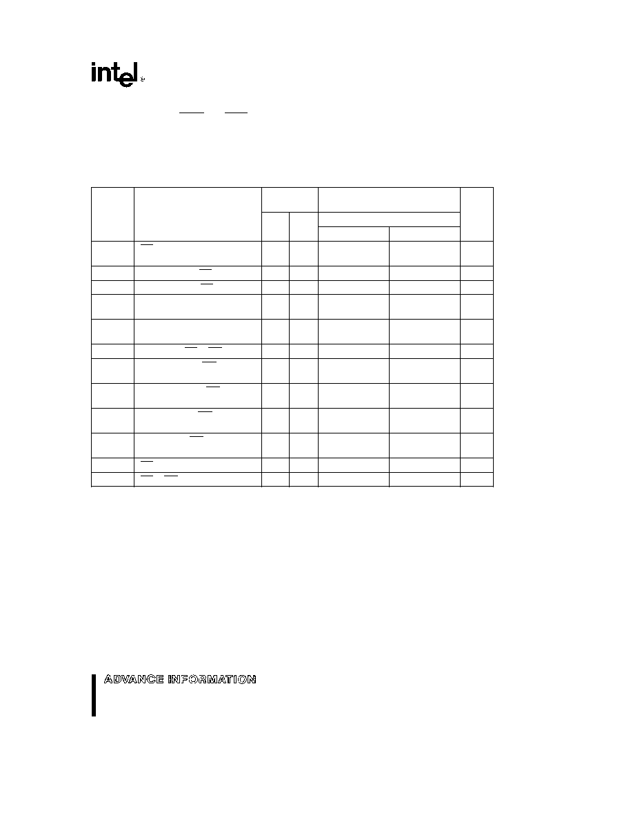
AUTOMOTIVE 87C51FA FB FC FC-20
AC CHARACTERISTICS
(T
A
e
b
40 C to a125 C V
CC
e
5V
g
20% V
SS
e
0V Load Capaci-
tance for Port 0 ALE PROG and PSEN e 100 pF Load Capacitance for All Other Outputs e 80 pF)
(Continued)
ADVANCED INFORMATION
CONTACT INTEL FOR DESIGN-IN INFORMATION
EXTERNAL PROGRAM MEMORY CHARACTERISTICS
(Continued)
Symbol
Parameter
12 MHz
Variable Oscillator
Units
Oscillator
Min
Max
87C51FA FB FC 87C51FC-20
Min
Max
T
RLDV
RD Low to Valid Data In
252
5T
CLCL
b
165
ns
5T
CLCL
b
95
T
RHDX
Data Hold After RD High
0
0
ns
T
RHDZ
Data Float After RD High
107
2T
CLCL
b
60
ns
T
LLDV
ALE Low to Valid Data In
517
8T
CLCL
b
150
ns
8T
CLCL
b
90
T
AVDV
Address Valid to Valid Data In
585
9T
CLCL
b
165
ns
9T
CLCL
b
90
T
LLWL
ALE Low to RD or WR Low
200
300
3T
CLCL
b
50
3T
CLCL
a
50
ns
T
AVWL
Address Valid to WR Low
203
4T
CLCL
b
130
ns
4T
CLCL
b
90
T
QVWX
Data Valid before WR Low
33
T
CLCL
b
50
ns
T
CLCL
b
35
T
WHQX
Data Hold after WR High
33
T
CLCL
b
50
ns
T
CLCL
b
40
T
QVWH
Data Valid to WR High
433
7T
CLCL
b
150
ns
7T
CLCL
b
70
T
RLAZ
RD Low to Address Float
0
0
ns
T
WHLH
RD or WR High to ALE High
43
123
T
CLCL
b
40
T
CLCL
a
40
ns
NOTE
Timings specified for the 87C51FC-20 are valid at 20 MHz only For timing information below 20 MHz use the 87C51FA
FB FC timings
11
AUTOMOTIVE 87C51FA FB FC FC-20
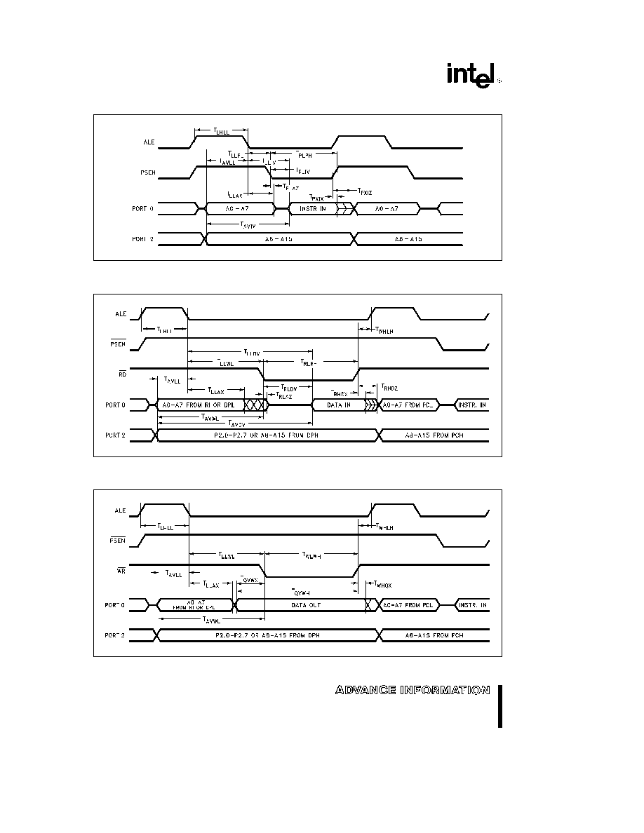
EXTERNAL PROGRAM MEMORY READ CYCLE
270961 ≠ 12
EXTERNAL DATA MEMORY READ CYCLE
270961 ≠ 13
EXTERNAL DATA MEMORY WRITE CYCLE
270961 ≠ 14
12
AUTOMOTIVE 87C51FA FB FC FC-20
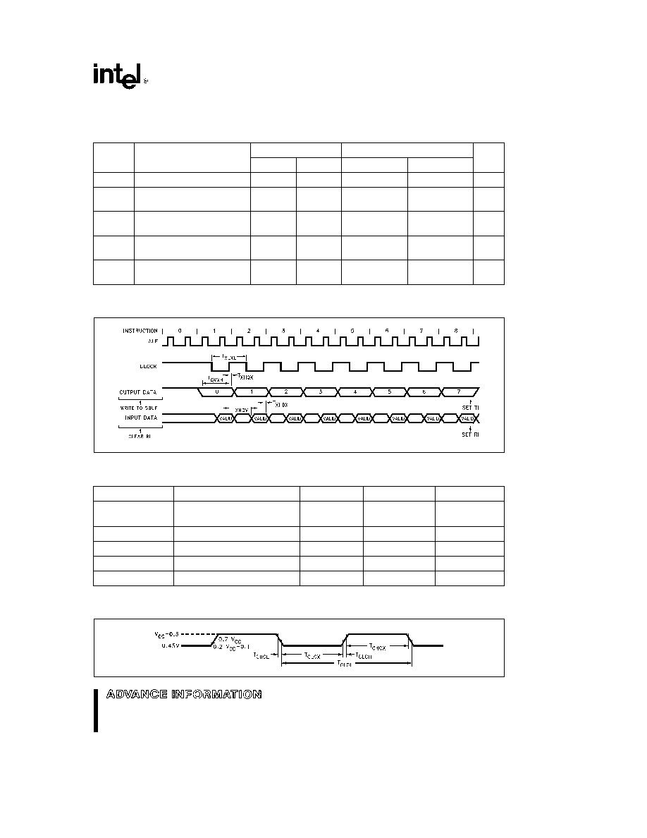
SERIAL PORT TIMING
SHIFT REGISTER MODE
Test Conditions
T
A
e b
40 C to a125 C V
CC
e
5V
g
20% V
SS
e
0V Load Capacitance e 80 pF
Symbol
Parameter
12 MHz Oscillator
Variable Oscillator
Units
Min
Max
Min
Max
T
XLXL
Serial Port Clock Cycle Time
1
12T
CLCL
m
s
T
QVXH
Output Data Setup to Clock
700
10T
CLCL
b
133
ns
Rising Edge
T
XHQX
Output Data Hold after
50
2T
CLCL
b
117
ns
Clock Rising Edge
T
XHDX
Input Data Hold After Clock
0
0
ns
Rising Edge
T
XHDV
Clock Rising Edge to Input
700
10T
CLCL
b
133
ns
Data Valid
SHIFT REGISTER MODE TIMING WAVEFORMS
270961 ≠ 15
EXTERNAL CLOCK DRIVE
Symbol
Parameter
Min
Max
Units
1 T
CLCL
Oscillator Frequency
3 5
16 20
MHz
87C51FA FB FC
T
CHCX
High Time
20
ns
T
CLCX
Low Time
20
ns
T
CLCH
Rise Time
20
ns
T
CHCL
Fall Time
20
ns
EXTERNAL CLOCK DRIVE WAVEFORMS
270961 ≠ 16
13
AUTOMOTIVE 87C51FA FB FC FC-20
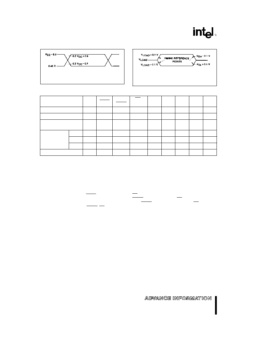
AC TESTING INPUT OUTPUT WAVEFORMS
270961 ≠ 17
AC Inputs during testing are driven at V
CC
b
0 5V for a Logic ``1''
and 0 45V for a Logic ``0'' Timing measurements are made at V
IH
min for a Logic ``1'' and V
IL
max for a Logic ``0''
FLOAT WAVEFORMS
270961 ≠ 18
For timing purposes a port pin is no longer floating when a
100 mV change from load voltage occurs and begins to float
when a 100 mV change from the loaded V
OH
V
OL
level occurs
I
OL
I
OH
t
g
20 mA
Table 3 EPROM Programming Modes
Mode
RST
PSEN
ALE
EA
P2 6
P2 7
P3 3
P3 6
P3 7
PROG
V
PP
Program Code Data
H
L
12 75V
L
H
H
H
H
Verify Code Data
H
L
H
H
L
L
L
H
H
Program Encryption
H
L
12 75V
L
H
H
L
H
Array Address 0 ≠ 3FH
Program Lock
Bit 1
H
L
12 75V
H
H
H
H
H
Bits
Bit 2
H
L
12 75V
H
H
H
L
L
Bit 3
H
L
12 75V
H
L
H
H
L
Read Signature Byte
H
L
H
H
L
L
L
L
L
DEFINITION OF TERMS
(EPROM PROGRAMMING)
ADDRESS LINES
P1 0 ≠ P1 7 P2 0 ≠ P2 5 P3 4 ≠
P3 5 respectively for A0 ≠ A13
DATA LINES
P0 0 ≠ P0 7 for D0 ≠ D7
CONTROL SIGNALS
RST PSEN P2 6 P2 7 P3 3
P3 6 P3 7
PROGRAM SIGNALS
ALE PROG EA V
PP
PROGRAMMING THE EPROM
The part must be running with a 4 MHz to 6 MHz
oscillator The address of an EPROM location to be
programmed is applied to address lines while the
code byte to be programmed in that location is ap-
plied to data lines Control and program signals must
be held at the levels indicated in Table 3 Normally
EA V
PP
is held at logic high until just before ALE
PROG is to be pulsed The EA V
PP
is raised to V
PP
ALE PROG is pulsed low and then EA V
PP
is re-
turned to a high (also refer to timing diagrams)
NOTE
Exceeding the V
PP
maximum for any amount of
time could damage the device permanently The
V
PP
source must be well regulated and free of
glitches
14

AUTOMOTIVE 87C51FA FB FC FC-20
270961 ≠ 19
See Table 2 for proper input on these pins
Figure 11 Programming the EPROM
PROGRAMMING ALGORITHM
Refer to Table 3 and Figures 11 and 12 for address
data and control signals set up To program the
87C51FA FB FC the following sequence must be
exercised
1 Input the valid address on the address lines
2 Input the appropriate data byte on the data lines
3 Activate the correct combination of control sig-
nals
4 Raise EA V
PP
from V
CC
to 12 75V
g
0 25V
5 Pulse ALE PROG 5 times for the EPROM array
and 25 times for the encryption table and the lock
bits
Repeat 1 through 5 changing the address and data
for the entire array or until the end of the object file is
reached
PROGRAM VERIFY
Program verify may be done after each byte or block
of bytes is programmed In either case a complete
verify of the programmed array will ensure reliable
programming of the 87C51FA FB FC
The lock bits cannot be directly verified Verification
of the lock bits is done by observing that their fea-
tures are enabled Refer to the EPROM Program
Lock section in this data sheet
270961 ≠ 20
5 Pulses
Figure 12 Programming Signal's Waveforms
15
AUTOMOTIVE 87C51FA FB FC FC-20
EPROM Program Lock
The 87C51FA FB FC program lock system when
programmed protects the onboard program against
software piracy
The 87C51FA FB FC has a 3-level program lock
system and a 64-byte encryption array Since this is
an EPROM device all locations are user program-
mable See Table 4
Program Lock Bits
The 87C51FA FB FC has 3 programmable lock bits
that when programmed according to Table 4 will
provide different levels of protection for the on-chip
code and data
Erasing the EPROM also erases the encryption ar-
ray and the program lock bits returning the part to
full functionality
Encryption Array
Within the EPROM array are 64 bytes of Encryption
Array that are initially unprogrammed (all 1's) Every
time that a byte is addressed during a verify 6 ad-
dress lines are used to select a byte of the Encryp-
tion Array
This byte is then exclusive-NOR'ed
(XNOR) with the code byte creating an Encryption
Verify byte The algorithm with the array in the un-
programmed state (all 1's) will return the code in it's
original unmodified form For programming the En-
cryption Array refer to Table 3 (EPROM Program-
ming Mode)
Reading the Signature Bytes
The 87C51FA FB FC has 3 signature bytes in loca-
tions 30H 31H and 60H To read these bytes follow
the procedure for EPROM verify but activate the
control lines provided in Table 3 for Read Signature
Byte
Location
30H e 89H
31H e 58H
60H e FBH (for an FB part)
60H e FCH (for an FC part)
Table 4 Program Lock Bits and the Features
Program Lock Bits
Protection Type
LB1
LB2
LB3
1
U
U
U
No Program Lock features enabled (Code verify will still be encrypted by the
Encryption Array if programmed )
2
P
U
U
MOVC instructions executed from external program memory are disabled
from fetching code bytes from internal memory EA is sampled and latched on
Reset and further programming of the EPROM is disabled
3
P
P
U
Same as 2 also verify is disabled
4
P
P
P
Same as 3 also external execution is disabled
Any other combination of the lock bits is not defined
16
AUTOMOTIVE 87C51FA FB FC FC-20
EPROM PROGRAMMING AND VERIFICATION CHARACTERISTICS
(T
A
e
21 C to 27 C V
CC
e
5V
g
20% V
SS
e
0V)
ADVANCED INFORMATION
CONTACT INTEL FOR DESIGN-IN INFORMATION
Symbol
Parameter
Min
Max
Units
V
PP
Programming Supply Voltage
12 5
13 0
V
I
PP
Programming Supply Current
75
mA
1 T
CLCL
Oscillator Frequency
4
6
MHz
T
AVGL
Address Setup to PROG Low
48T
CLCL
T
GHAX
Address Hold after PROG
48T
CLCL
T
DVGL
Data Setup to PROG Low
48T
CLCL
T
GHDX
Data Hold after PROG
48T
CLCL
T
EHSH
(Enable) High to V
PP
48T
CLCL
T
SHGL
V
PP
Setup to PROG Low
10
m
s
T
GHSL
V
PP
Hold after PROG
10
m
s
T
GLGH
PROG Width
90
110
m
s
T
AVQV
Address to Data Valid
48T
CLCL
T
ELQV
ENABLE Low to Data Valid
48T
CLCL
T
EHQZ
Data Float after ENABLE
0
48T
CLCL
T
GHGL
PROG High to PROG Low
10
m
s
EPROM PROGRAMMING AND VERIFICATION WAVEFORMS
270961 ≠ 21
17

AUTOMOTIVE 87C51FA FB FC FC-20
DATA SHEET REVISION HISTORY
The following are key differences between this data sheet and the -002 revision of the data sheet
1 The data sheet has been revised from the 87C51FB 87C51FC to the 87C51FA 87C51FB 87C51FC
87C51FC-20 and includes the 20 MHz 87C51FC
2 RST pin in Figure 3 has been changed to RESET pin
3 Reference to Application Note AP-486 was added on page 5
4 The I
CC
specification has been corrected in the D C Characteristics section
5 The 20 MHz I
CC
max values have been added
6 20 MHz 87C51FC timings information were added to the External Program Memory Characteristics table
DATA SHEET REVISION HISTORY
The following are key differences between this data sheet and the -001 version of the data sheet
1 ``NC'' pin labels changed to ``Reserved'' in Figure 3
2 Capacitor value for ceramic resonators deleted in Figure 4
3 Replaced A0 ≠ A15 with P1 0 ≠ P1 7 P2 0 ≠ P2 5 (EPROM programming and verification waveforms)
4 Replaced D0 ≠ D7 with P0 (EPROM programming and verification waveforms)
5 Combined the 87C51FB and 87C51FC data sheets
The following are the key differences between the previous 87C51FB data sheet versions and this new data
sheet (rev-001)
1 The data sheet has been revised from a 83C51FB 87C51FB to an 87C51FB data sheet only
2 The data sheet has been revised to specify AC and DC parameters to V
CC
e
5V
g
20% instead of V
CC
e
5V
g
10%
3 The 87C51FB is now offered in a 3 5 MHz ≠ 20 MHz version
4 The RST description has been modified to clarify the reset operation when the oscillator is not running
5 Figure 4 (Oscillator Connections) has been changed for Ceramic Resonators
6 A description of RFI Reduction Mode has been added
7 V
OH1
I
IL
I
TL
and I
CC
DC Characteristics have been revised
8 Note 1 of the DC Characteristics has been clarified
9 The External Clock Drive diagram has been modified to include 16 MHz and 20 MHz device types
10 The Float Waveforms diagram has been revised for greater clarity
11 Table 4 EPROM Programming Modes has been modified included logic levels for P3 3 and three pro-
gram lock bits
12 The Encryption Array section now states that six address lines are used to select a byte from the Encryp-
tion Array instead of five
13 The I
PP
specification in the EPROM Programming and Verification Characteristics has been increased to
75 mA
18