 | –≠–ª–µ–∫—Ç—Ä–æ–Ω–Ω—ã–π –∫–æ–º–ø–æ–Ω–µ–Ω—Ç: 87L58 | –°–∫–∞—á–∞—Ç—å:  PDF PDF  ZIP ZIP |

Other brands and names are the property of their respective owners
Information in this document is provided in connection with Intel products Intel assumes no liability whatsoever including infringement of any patent or
copyright for sale and use of Intel products except as provided in Intel's Terms and Conditions of Sale for such products Intel retains the right to make
changes to these specifications at any time without notice Microcomputer Products may have minor variations to this specification known as errata
November 1994
COPYRIGHT
INTEL CORPORATION 1995
Order Number 272468-002
8XL52 54 58
LOW VOLTAGE
CHMOS SINGLE-CHIP 8-BIT MICROCONTROLLERS
Commercial Express
87L52 80L52 87L54 80L54 87L58 80L58
Y
High Performance CHMOS OTP ROM
Y
Low Voltage Operation
Y
20 MHz Commercial 16 MHz Express
Operation
Y
Three 16-Bit Timer Counters
Y
Up Down Timer Counter
Y
Three Level Program Lock System
Y
8K 16K 32K On-Chip Program Memory
Y
256 Bytes of On-Chip Data RAM
Y
Improved Quick Pulse Programming
Algorithm
Y
Boolean Processor
Y
32 Programmable I O Lines
Y
6 Interrupt Sources
Y
Four Level Interrupt Priority
Y
Programmable Serial Channel with
Framing Error Detection
Automatic Address Recognition
Y
64K External Program Memory Space
Y
64K External Data Memory Space
Y
MCS
51 Microcontroller Compatible
Instruction Set
Y
Power Saving Idle and Power Down
Modes
Y
ONCE (On-Circuit Emulation) Mode
Y
Extended Temperature Range
(
b
40 C to
a
85 C)
MEMORY ORGANIZATION
OTP ROM
Version
Version
ROM
ROM
Bytes
RAM
OTP ROM
Bytes
87L52
80L52
8K
256
87L54
80L54
16K
256
87L58
80L58
32K
256
These devices can address up to 64 Kbytes of external program data memory
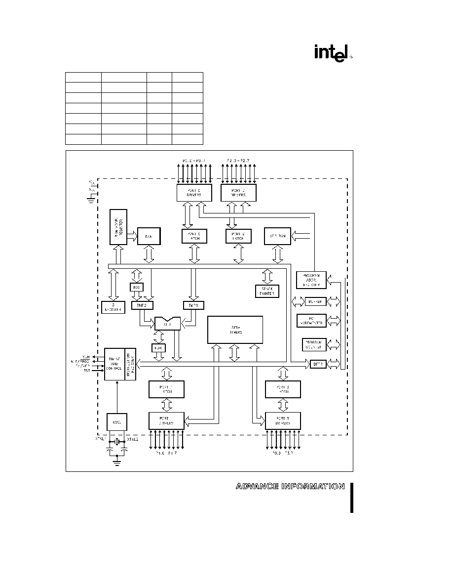
The Intel 8XL52 8XL54 8XL58 is a single-chip control oriented microcontroller which is fabricated on Intel's
reliable CHMOS III-E technology Being a member of the MCS 51 microcontroller family the 8XL52 8XL54
8XL58 uses the same powerful instruction set has the same architecture and is pin-for-pin compatible with
the existing MCS 51 microcontroller products
The 8XL5X is a 3V version of current 8XC5X and will operate from 2 7V to 3 6V at a frequency range of
3 5 MHz to 16 MHz (Express) 20 MHz (Commercial)
For the remainder of this document the 8XL52 8XL54 8XL58 will be referred to as the 8XL5X unless
information applies to a specific device
8XL52 54 58
Standard
-1
-20
80L52
X
X
X
87L52
X
X
X
80L54
X
X
X
87L54
X
X
X
80L58
X
X
X
87L58
X
X
X
NOTE
Standard
3 5 MHz to 12 MHz 2 7V to 3 6V
-1
3 5 MHz to 16 MHz 2 7V to 3 6V
-20
3 5 MHz to 20 MHz 2 7V to 3 6V
Only available for commercial standard temperature range not avail-
able at express temperature range
272468 ≠ 1
Figure 1 8XL5X Block Diagram
2
8XL52 54 58
PROCESS INFORMATION
The
8XL52 8XL54 8XL58
is
manufactured
on
P629 5 a CHMOS III-E process Additional process
and reliability information is available in Intel's
Com-
ponents Quality and Reliability Handbook
Order
Number 210997
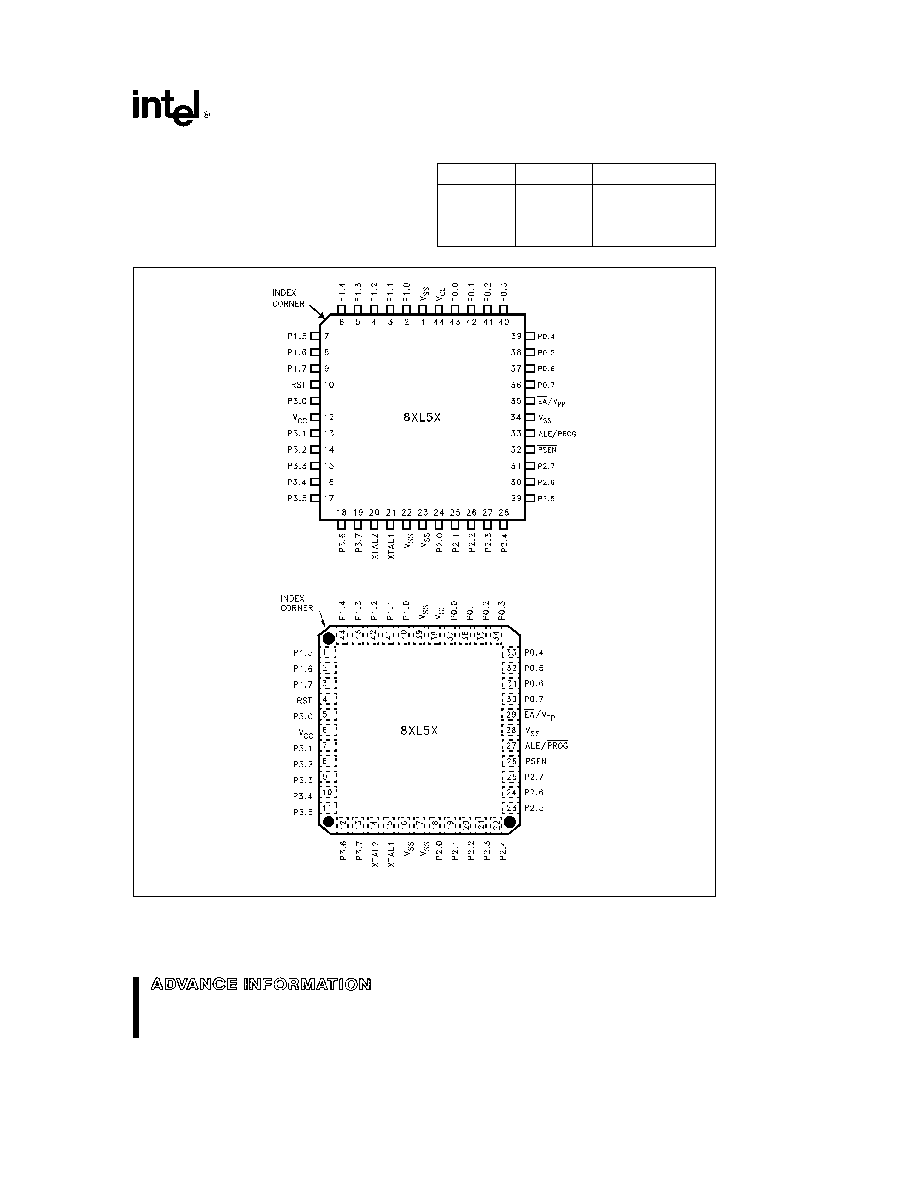
PACKAGES
Part
Prefix
Package Type
8XL5X
N
44-Pin PLCC
(OTP)
S
44-Pin QFP
(OTP)
272468 ≠ 2
PLCC
272468 ≠ 3
QFP
Figure 2 Pin Connections
3
8XL52 54 58
PIN DESCRIPTIONS
V
CC
Supply voltage
V
SS
Circuit ground
Port 0 Port 0 is an 8-bit open drain bidirectional I O
port As an output port each pin can sink several
inputs Port 0 pins that have 1's written to them float
and in that state can be used as high-impedance
inputs
Port 0 is also the multiplexed low-order address and
data bus during accesses to external Program and
Data Memory In this application it uses strong inter-
nal pullups when emitting 1's and can source and
sink several inputs
Port 0 also receives the code bytes during OTP
ROM programming and outputs the code bytes dur-
ing program verification External pullup resistors are
required during program verification
Port 1 Port 1 is an 8-bit bidirectional I O port with
internal pullups The Port 1 output buffers can drive
several inputs Port 1 pins that have 1's written to
them are pulled high by the internal pullups and in
that state can be used as inputs As inputs Port 1
pins that are externally pulled low will source current
(I
IL
on the data sheet) because of the internal pull-
ups
In addition Port 1 serves the functions of the follow-
ing special features of the 8XL5X
Port Pin
Alternate Function
P1 0
T2 (External Count
Input to Timer
Counter 2) Clock
Out
P1 1
T2EX (Timer
Counter 2 Capture
Reload Trigger and
Direction Control)
Port 1 receives the low-order address bytes during
OTP ROM programming and verifying
Port 2 Port 2 is an 8-bit bidirectional I O port with
internal pullups The Port 2 output buffers can drive
several inputs Port 2 pins that have 1's written to
them are pulled high by the internal pullups and in
that state can be used as inputs As inputs Port 2
pins that are externally pulled low will source current
(I
IL
on the data sheet) because of the internal pull-
ups
Port 2 emits the high-order address byte during
fetches from external Program Memory and during
accesses to external Data Memory that use 16-bit
addresses (MOVX
DPTR) In this application it
uses strong internal pullups when emitting 1's Dur-
ing accesses to external Data Memory that use 8-bit
addresses (MOVX
Ri) Port 2 emits the contents of
the P2 Special Function Register
Some Port 2 pins receive the high-order address bits
during OTP ROM programming and program verifi-
cation
Port 3 Port 3 is an 8-bit bidirectional I O port with
internal pullups The Port 3 output buffers can drive
several inputs Port 3 pins that have 1's written to
them are pulled high by the internal pullups and in
that state can be used as inputs As inputs Port 3
pins that are externally pulled low will source current
(I
IL
on the data sheet) because of the pullups
Port 3 also serves the functions of various special
features of the MCS-51 Family as listed below
Port Pin
Alternate Function
P3 0
RXD (serial input port)
P3 1
TXD (serial output port)
P3 2
INT0 (external interrupt 0)
P3 3
INT1 (external interrupt 1)
P3 4
T0 (Timer 0 external input)
P3 5
T1 (Timer 1 external input)
P3 6
WR (external data memory write strobe)
P3 7
RD (external data memory read strobe)
RST Reset input A high on this pin for two machine
cycles while the oscillator is running resets the de-
vice The port pins will be driven to their reset condi-
tion when a minimum V
IH2
voltage is applied wheth-
er the oscillator is running or not An internal pull-
down resistor permits a power-on reset with only a
capacitor connected to V
CC
4
8XL52 54 58
ALE Address Latch Enable output pulse for latching
the low byte of the address during accesses to ex-
ternal memory This pin (ALE PROG) is also the
program pulse input during OTP ROM programming
for the 87L5X
In normal operation ALE is emitted at a constant
rate of
the oscillator frequency and may be used
for external timing or clocking purposes Note how-
ever that one ALE pulse is skipped during each ac-
cess to external Data Memory
If desired ALE operation can be disabled by setting
bit 0 of SFR location 8EH With this bit set the pin is
weakly pulled high However the ALE disable fea-
ture will be suspended during a MOVX or MOVC in-
struction idle mode power down mode and ICE
mode The ALE disable feature will be terminated by
reset When the ALE disable feature is suspended or
terminated the ALE pin will no longer be pulled up
weakly Setting the ALE-disable bit has no affect if
the microcontroller is in external execution mode
Throughout the remainder of this data sheet ALE
will refer to the signal coming out of the ALE PROG
pin and the pin will be referred to as the ALE PROG
pin
PSEN Program Store Enable is the read strobe to
external Program Memory
When the 8XL5X is executing code from external
Program Memory PSEN is activated twice each ma-
chine cycle except that two PSEN activations are
skipped during each access to external Data Memo-
ry
EA V
PP
External Access enable
EA must be
strapped to VSS in order to enable the device to
fetch code from external Program Memory locations
0000H to 0FFFH Note however that if either of the
Program Lock bits are programmed EA will be inter-
nally latched on reset
EA must be strapped to V
CC
for internal program
executions
This pin also receives the programming supply volt-
age (V
PP
) during OTP ROM programming
XTAL1 Input to the inverting oscillator amplifier
XTAL2 Output from the inverting oscillator amplifier
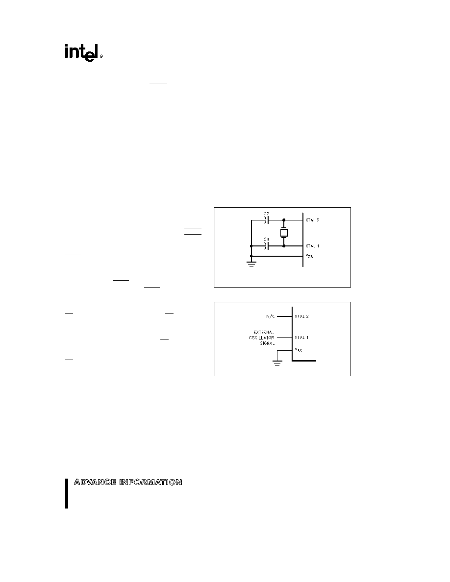
OSCILLATOR CHARACTERISTICS
XTAL1 and XTAL2 are the input and output respec-
tively of a inverting amplifier which can be config-
ured for use as an on-chip oscillator as shown in
Figure 3 Either a quartz crystal or ceramic resonator
may be used More detailed information concerning
the use of the on-chip oscillator is available in Appli-
cation Note AP-155 ``Oscillators for Microcontrol-
lers ''
To drive the device from an external clock source
XTAL1 should be driven while XTAL2 floats as
shown in Figure 4 There are no requirements on the
duty cycle of the external clock signal since the in-
put to the internal clocking circuitry is through a di-
vide-by-two flip-flop but minimum and maximum
high and low times specified on the data sheet must
be observed
An external oscillator may encounter as much as a
100 pF load at XTAL1 when it starts up This is due
to interaction between the amplifier and its feedback
capacitance Once the external signal meets the V
IL
and V
IH
specifications the capacitance will not ex-
ceed 20 pF
272468 ≠ 4
C1 C2 e 30 pF
g
10 pF for Crystals
For Ceramic Resonators contact resonator manufacturer
Figure 3 Oscillator Connections
272468 ≠ 5
Figure 4 External Clock Drive Configuration
IDLE MODE
The user's software can invoke the Idle Mode When
the microcontroller is in this mode power consump-
tion is reduced The Special Function Registers and
the onboard RAM retain their values during Idle but
the processor stops executing instructions
Idle
Mode will be exited if the chip is reset or if an en-
abled interrupt occurs The PCA timer counter can
optionally be left running or paused during Idle
Mode
5
8XL52 54 58
POWER DOWN MODE
To save even more power a Power Down mode can
be invoked by software In this mode the oscillator
is stopped and the instruction that invoked Power
Down is the last instruction executed The on-chip
RAM and Special Function Registers retain their val-
ues until the Power Down mode is terminated
On the 8XL5X either hardware reset or external in-
terrupt can cause an exit from Power Down Reset
redefines all the SFRs but does not change the on-
chip RAM An external interrupt allows both the
SFRs and the on-chip RAM to retain their values
To properly terminate Power Down the reset or ex-
ternal interrupt should not be executed before V
CC
is
restored to its normal operating level and must be
held active long enough for the oscillator to restart
and stabilize (normally less than 10 ms)
With an external interrupt INT0 or INT1 must be en-
abled and configured as level-sensitive Holding the
pin low restarts the oscillator but bringing the pin
back high completes the exit Once the interrupt is
serviced the next instruction to be executed after
RETI will be the one following the instruction that put
the device into Power Down
DESIGN CONSIDERATION
The 8XL5X will operate from 2 7V to 3 6V with a
frequency range of 3 5 MHz to 16 MHz (Ex-
press) 20 MHz (Commercial) Operating beyond
these specifications could cause improper device
functionality
All V
CC
and V
SS
pins must be connected Please
refer to Figure 2 Pin Connections for the specific
pins
When the idle mode is terminated by a hardware
reset the device normally resumes program exe-
cution from where it left off up to two machine
cycles before the internal reset algorithm takes
control On-chip hardware inhibits access to inter-
nal RAM in this event but access to the port pins
is not inhibited To eliminate the possibility of an
unexpected write when Idle is terminated by re-
set the instruction following the one that invokes
Idle should not be one that writes to a port pin or
to external memory
ONCE MODE
The ONCE (``On-Circuit Emulation'') Mode facilitates
testing and debugging of systems using the 8XL5X
without the 8XL5X having to be removed from the
circuit The ONCE Mode is invoked by
1) Pull ALE low while the device is in reset and
PSEN is high
2) Hold ALE low as RST is deactivated
While the device is in ONCE Mode the Port 0 pins
float and the other port pins and ALE and PSEN are
weakly pulled high The oscillator circuit remains ac-
tive While the 8XL5X is in this mode an emulator or
test CPU can be used to drive the circuit Normal
operation is restored when a normal reset is applied
Table 1 Status of the External Pins during Idle and Power Down
Mode
Program
ALE
PSEN
PORT0
PORT1
PORT2
PORT3
Memory
Idle
Internal
1
1
Data
Data
Data
Data
Idle
External
1
1
Float
Data
Address
Data
Power Down
Internal
0
0
Data
Data
Data
Data
Power Down
External
0
0
Float
Data
Data
Data
NOTE
For more detailed information on the reduced power modes refer to current Embedded Microcontrollers and Processors
Handbook Volume I
270646 and Application Note AP-252 (Embedded Applications Handbook)
270648 ``Designing
with the 80C51BH ''
6
8XL52 54 58
8XL5X EXPRESS
The Intel EXPRESS system offers enhancements to
the operational specifications of the MCS-51 family
of microcontrollers These EXPRESS products are
designed to meet the needs of those applications
whose operating requirements exceed commercial
standards
The EXPRESS program includes the commercial
standard temperature range with burn-in and an ex-
tended temperature range with or without burn-in
With the commercial standard temperature range
operational characteristics are guaranteed over the
temperature range of 0 C to 70 C With the extend-
ed temperature range option operational character-
istics are guaranteed over the range of b40 C to
a
85 C
Package types and EXPRESS versions are identified
by a one- or two-letter prefix to the part number The
prefixes are listed in Table 2
For the extended temperature range option this
data sheet specifies the parameters which deviate
from their commercial temperature range limits
Table 2 Prefix Identification
Prefix
Package
Temperature
Type
Range
N
PLCC
Commercial
S
QFP
Commercial
TN
PLCC
Extended
TS
QFP
Extended
NOTE
Contact your distributor or local sales office to match the
EXPRESS prefix with the proper device
EXAMPLES
N87L51FC indicates 87L51FC in a PLCC package and
specified for commercial temperature range without burn-
in
TN87L51FC indicates 87L51FC in a PLCC package
and specified for extended temperature range with
burn-in
7
8XL52 54 58
ABSOLUTE MAXIMUM RATINGS
Ambient Temperature Under Bias b40 C to a85 C
Storage Temperature
b
65 C to a150 C
Voltage on EA V
PP
Pin to V
SS
0V to a13 0V
Voltage on Any Other Pin to V
SS
b
0 5V to a6 5V
I
OL
per I O Pin
15 mA
Power Dissipation
1 5W
(based on PACKAGE heat transfer limitations not
device power consumption)
NOTICE This data sheet contains information on
products in the sampling and initial production phases
of development It is valid for the devices indicated in
the revision history The specifications are subject to
change without notice
WARNING Stressing the device beyond the ``Absolute
Maximum Ratings'' may cause permanent damage
These are stress ratings only Operation beyond the
``Operating Conditions'' is not recommended and ex-
tended exposure beyond the ``Operating Conditions''
may affect device reliability
OPERATING CONDITIONS
Symbol
Description
Min
Max
Units
T
A
Ambient Temperature Under Bias
Commercial
0
a
70
C
Express
b
40
a
85
C
V
CC
Supply Voltage
2 7
3 6
V
DC CHARACTERISTICS
(Over Operating Conditions)
All parameter values apply to all devices unless otherwise indicated
Symbol
Parameter
Min
Max
Units
Test Conditions
V
IL
Input Low Voltage
b
0 5
0 8
V
(except XTAL1 RST)
V
IL1
Input Low Voltage
b
0 5
0 2 V
CC
b
0 1
V
(XTAL1 RST)
V
IH
Input High Voltage
2 0
V
CC
a
0 5
V
(Except XTAL1 RST EA)
V
IH1
Input High Voltage (EA)
V
CC
b
1 0
V
CC
a
0 5
V
V
IH2
Input High Voltage
0 7 V
CC
V
CC
a
0 5
V
(XTAL1 RST)
V
OL
Output Low Voltage (Note 4)
0 4
V
I
OL
e
1 6 mA (Note 1)
(Ports 1 2 and 3)
V
OL1
Output Low Voltage (Note 4)
0 4
V
I
OL
e
3 2 mA
(Port 0 ALE PSEN)
(Note 1)
V
OH
Output High Voltage
V
CC
b
0 7
V
I
OH
e b
30 mA
(Ports 1 2 and 3 ALE PSEN
(Note 2)
V
OH1
Output High Voltage
2 4
V
I
OH
e b
1 0 mA
(Port 0 in External Bus Mode)
(Note 2)
I
IL
Logical 0 Input Current
b
50
m
A
V
IN
e
0 4V
(Ports 1 2 and 3)
I
LI
Input Leakage Current (Port 0)
g
10
m
A
0
k
V
IN
k
V
CC
8
8XL52 54 58
DC CHARACTERISTICS
(Over Operating Conditions)
All parameter values apply to all devices unless otherwise indicated (Continued)
Symbol
Parameter
Min
Max
Units
Test Conditions
I
TL
Logical 1 to 0
b
350
m
A
V
IN
e
1 4V
Transition Current
(Ports 1 2 and 3)
RRST
RST Pulldown Resistor
40
225
KX
I
CC
Power Supply Current
(Note 3)
Active Mode at 16 MHz
25
mA
Idle Mode at 16 MHz
8
mA
Power-Down Mode
30
m
A
NOTES
1 Capacitive loading on Ports 0 and 2 may cause noise pulses above 0 4V to be superimposed on the V
OL
s of ALE and
Ports 1 2 and 3 The noise is due to external bus capacitance discharging into the Port 0 and Port 2 pins when these pins
change from 1 to 0 In applications where capacitance loading exceeds 100 pF the noise pulses on these signals may
exceed 0 8V It may be desirable to qualify ALE or other signals with a Schmitt Trigger or CMOS-level input logic
2 Capacitive loading on Ports 0 and 2 cause the V
OH
on ALE and PSEN to drop below the 0 9 V
CC
specification when the
address lines are stabilizing
3 See Figures 6 ≠ 9 for test conditions Minimum V
CC
for power down is 2V
4 Under steady state (non-transient) conditions I
OL
must be externally limited as follows
Maximum I
OL
per port pin
10 mA
Maximum I
OL
per 8-bit port -
Port 0
26 mA
Ports 1 2 and 3
15 mA
Maximum total I
OL
for all output pins
71 mA
If I
OL
exceeds the test condition V
OL
may exceed the related specification Pins are not guaranteed to sink current greater
than the listed test conditions
Running the device with EA at a higher voltage than V
CC
sinks additional currrent
272468 ≠ 6
I
CC
Max at other frequencies (3 5 MHz to 20 MHz) is given by
Active Mode
I
CC
MAX e 1 1
c
FREQ a 7 6
Idle Mode
I
CC
MAX e 0 4
c
FREQ a 1 8
Where FREQ is in MHz I
CC
MAX is given in mA
Figure 5 I
CC
vs Frequency
9
8XL52 54 58
272468 ≠ 7
All other pins disconnected
TCLCH e TCHCL e 5 ns
Figure 6 I
CC
Test Condition Active Mode
272468 ≠ 8
All other pins disconnected
TCLCH e TCHCL e 5 ns
Figure 7 I
CC
Test Condition Idle Mode
272468 ≠ 9
All other pins disconnected
Figure 8 I
CC
Test Condition Power Down Mode
V
CC
e
2 7V to 3 6V
272468 ≠ 10
Figure 9 Clock Signal Waveform for I
CC
Tests in Active and Idle Modes TCLCH e TCHCL e 5 ns
10
8XL52 54 58
EXPLANATION OF THE AC SYMBOLS
Each timing symbol has 5 characters The first char-
acter is always a `T' (stands for time) The other
characters depending on their positions stand for
the name of a signal or the logical status of that
signal The following is a list of all the characters and
what they stand for
A Address
C Clock
D Input Data
H Logic level HIGH
I Instruction (program memory contents)
L Logic level LOW or ALE
P PSEN
Q Output Data
R RD signal
T Time
V Valid
W WR signal
X No longer a valid logic level
Z Float
For example
TAVLL e Time from Address Valid to ALE Low
TLLPL e Time from ALE Low to PSEN Low
AC CHARACTERISTICS
(Over Operating Conditions Load Capacitance for Port 0 ALE PROG and
PSEN e 100 pF Load Capacitance for All Other Outputs e 80 pF)
EXTERNAL MEMORY CHARACTERISTICS
All parameter values apply to all devices unless otherwise indicated In this table 8XL5X refers to 8XL5X and
8XL5X-1
Symbol
Parameter
12 MHz
20 MHz
Variable
Units
Oscillator
Oscillator
Oscillator
Min
Max
Min
Max
Min
Max
1 TCLCL
Oscillator Frequency
8XL5X
3 5
12
MHz
8XL5X-1
3 5
16
MHz
8XL5X-20
3 5
20
MHz
TLHLL
ALE Pulse Width
127
60
2 TCLCL b 40
ns
TAVLL
Address Valid to
43
10
TCLCL b 40
ns
ALE Low
TLLAX
Address Hold After
53
20
TCLCL b 30
ns
ALE Low
TLLIV
ALE Low to Valid
Instruction In
8XL5X
234
4 TCLCL b 100
ns
8XL5X-20
125
4 TCLCL b 75
ns
TLLPL
ALE Low to PSEN
53
20
TCLCL b 30
ns
Low
TPLPH
PSEN Pulse Width
205
105
3 TCLCL b 45
ns
TPLIV
PSEN Low to Valid
Instruction In
8XL5X
145
3 TCLCL b 105
ns
8XL5X-20
60
3 TCLCL b 90
ns
TPXIX
Input Instruction
0
0
0
ns
Hold After PSEN
11
8XL52 54 58
EXTERNAL MEMORY CHARACTERISTICS
(Continued)
All parameter values apply to all devices unless otherwise indicated
Symbol
Parameter
12 MHz
20 MHz
Variable
Units
Oscillator
Oscillator
Oscillator
Min
Max
Min
Max
Min
Max
TPXIZ
Input Instruction Float
After PSEN
8XL5X
59
TCLCL
b
25
ns
8XL5X-20
30
TCLCL
b
20
ns
TAVIV
Address to Valid
312
145
5 TCLCL
b
105
ns
Instruction In
TPLAZ
PSEN Low to Address
10
10
10
ns
Float
TRLRH
RD Pulse Width
400
200
6 TCLCL
b
100
ns
TWLWH
WR Pulse Width
400
200
6 TCLCL
b
100
ns
TRLDV
RD Low to Valid Data In
8XL5X
252
5 TCLCL
b
165
ns
8XL5X-20
155
5 TCLCL
b
95
ns
TRHDX
Data Hold After RD
0
0
0
ns
TRHDZ
Data Float After RD
107
40
2 TCLCL
b
60
ns
TLLDV
ALE Low to Valid Data In
8XL5X
517
8 TCLCL
b
150
ns
8XL5X-20
310
8 TCLCL
b
90
ns
TAVDV
Address to Valid Data In
8XL5X
585
9 TCLCL
b
165
ns
8XL5X-20
360
9 TCLCL
b
90
ns
TLLWL
ALE Low to RD or WR
200
300
100
200
3 TCLCL
b
50
3 TCLCL
a
50
ns
Low
TAVWL
Address Valid to WR
Low
8XL5X
203
4 TCLCL
b
130
ns
8XL5X-20
110
4 TCLCL
b
90
ns
TQVWX
Data Valid before WR
8XL5X
33
TCLCL
b
50
ns
8XL5X-20
15
TCLCL
b
35
ns
TWHQX
Data Hold after WR
8XL5X
33
TCLCL
b
50
ns
8XL5X-20
10
TCLCL
b
40
ns
TQVWH
Data Valid to WR High
8XL5X
433
7 TCLCL
b
150
ns
8XL5X-20
280
7 TCLCL
b
70
ns
TRLAZ
RD Low to Address Float
0
0
0
ns
TWHLH
RD or WR High to ALE
43
123
10
90
TCLCL
b
40
TCLCL
a
40
ns
High
12
8XL52 54 58
EXTERNAL PROGRAM MEMORY READ CYCLE
272468 ≠ 11
EXTERNAL DATA MEMORY READ CYCLE
272468 ≠ 12
EXTERNAL DATA MEMORY WRITE CYCLE
272468 ≠ 13
13

8XL52 54 58
SERIAL PORT TIMING - SHIFT REGISTER MODE
Test Conditions
Over Operating Conditions Load Capacitance e 80 pF
Symbol
Parameter
12 MHz
20 MHz
Variable
Units
Oscillator
Oscillator
Oscillator
Min
Max
Min
Max
Min
Max
TXLXL
Serial Port Clock
1
0 600
12 TCLCL
m
s
Cycle Time
TQVXH
Output Data Setup to
700
367
10 TCLCL
b
133
ns
Clock Rising Edge
TXHQX
Output Data Hold
after Clock Rising
Edge
8XL5X
50
2 TCLCL
b
117
ns
8XL5X-20
50
2 TCLCL
b
50
ns
TXHDX
Input Data Hold After
0
0
0
ns
Clock Rising Edge
TXHDV
Clock Rising Edge to
700
367
10 TCLCL
b
133
ns
Input Data Valid
SHIFT REGISTER MODE TIMING WAVEFORMS
272468 ≠ 14
14

8XL52 54 58
EXTERNAL CLOCK DRIVE
Symbol
Parameter
Min
Max
Units
1 TCLCL
Oscillator Frequency
8XL5X
3 5
12
MHz
8XL5X-1
3 5
16
8XL5X-20
3 5
20
TCHCX
High Time
20
ns
TCLCX
Low Time
20
ns
TCLCH
Rise Time
20
ns
TCHCL
Fall Time
20
ns
EXTERNAL CLOCK DRIVE WAVEFORM
272468 ≠ 15
AC TESTING INPUT OUTPUT WAVEFORMS
272468 ≠ 16
AC Inputs during testing are driven at V
CC
b
0 5V for a Logic ``1''
and 0 45V for a Logic ``0'' Timing measurements are made at V
IH
min for a Logic ``1'' and V
IL
max for a Logic ``0''
FLOAT WAVEFORMS
272468 ≠ 17
For timing purposes a port pin is no longer floating when a
100 mV change from load voltage occurs and begins to float
when a 100 mV change from the loaded V
OH
V
OL
level occurs
I
OL
I
OH
e
g
20 mA (-L I
OL
I
OH
e
g
10 mA)
15

8XL52 54 58
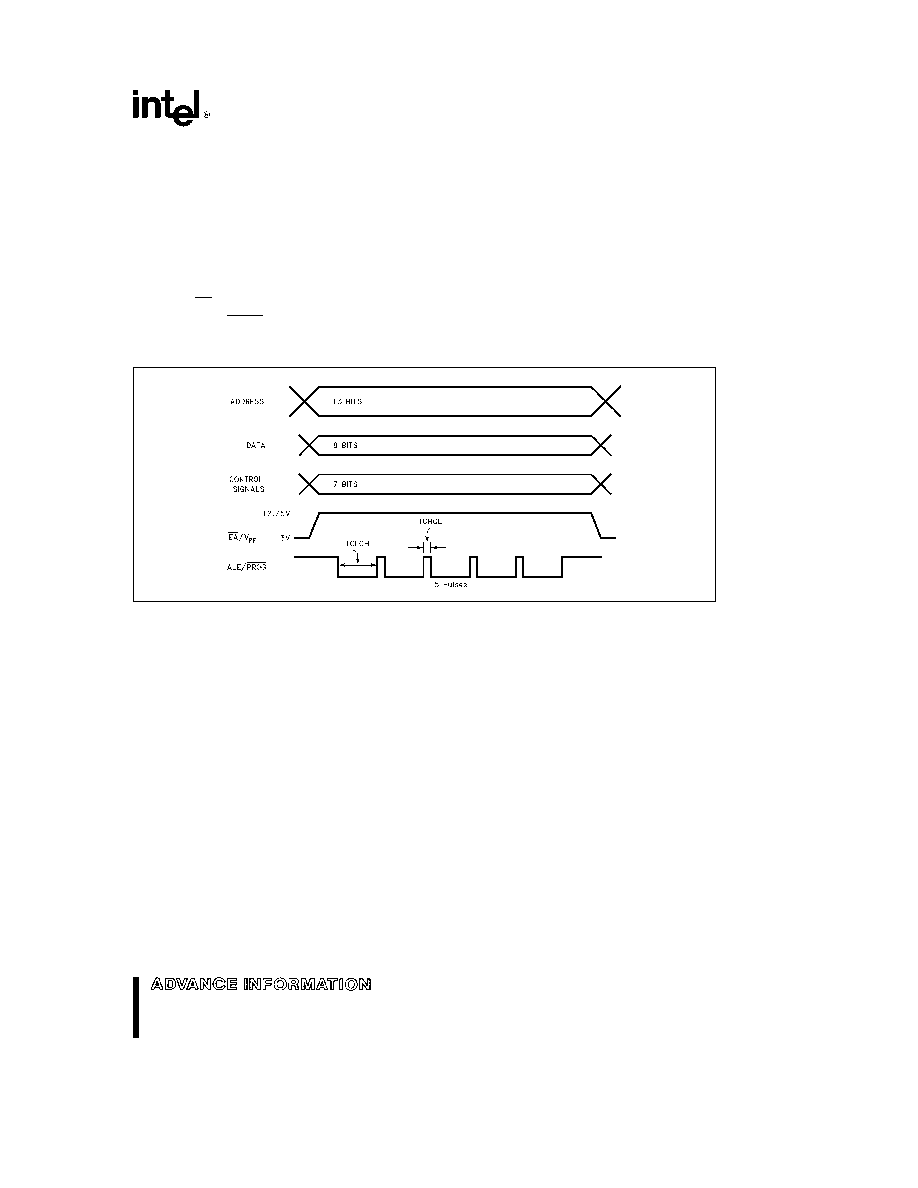
PROGRAMMING THE OTP ROM
To be programmed the part must be running with a
4 to 6 MHz oscillator (The reason the oscillator
needs to be running is that the internal bus is being
used to transfer address and program data to appro-
priate internal OTP ROM locations ) The address of
an OTP ROM location to be programmed is applied
to Port 1 and pins P2 0 - P2 4 of Port 2 while the
code byte to be programmed into that location is
applied to Port 0 The other Port 2 and 3 pins RST
PSEN and EA V
PP
should be held at the ``Program''
levels indicated in Table 3 ALE PROG is pulsed low
to program the code byte into the addressed OTP
ROM location The setup is shown in Figure 10
Normally EA V
PP
is held at logic high until just be-
fore ALE PROG is to be pulsed Then EA V
PP
is
raised to V
PP
ALE PROG is pulsed low and then
EA V
PP
is returned to a valid high voltage The volt-
age on the EA V
PP
pin must be at the valid EA V
PP
high level before a verify is attempted Waveforms
and detailed timing specifications are shown in later
sections of this data sheet
NOTE
EA V
PP
pin must not be allowed to go above the
maximum specified V
PP
level for any amount of
time Even a narrow glitch above that voltage lev-
el can cause permanent damage to the device
The V
PP
source should be well regulated and free
of glitches
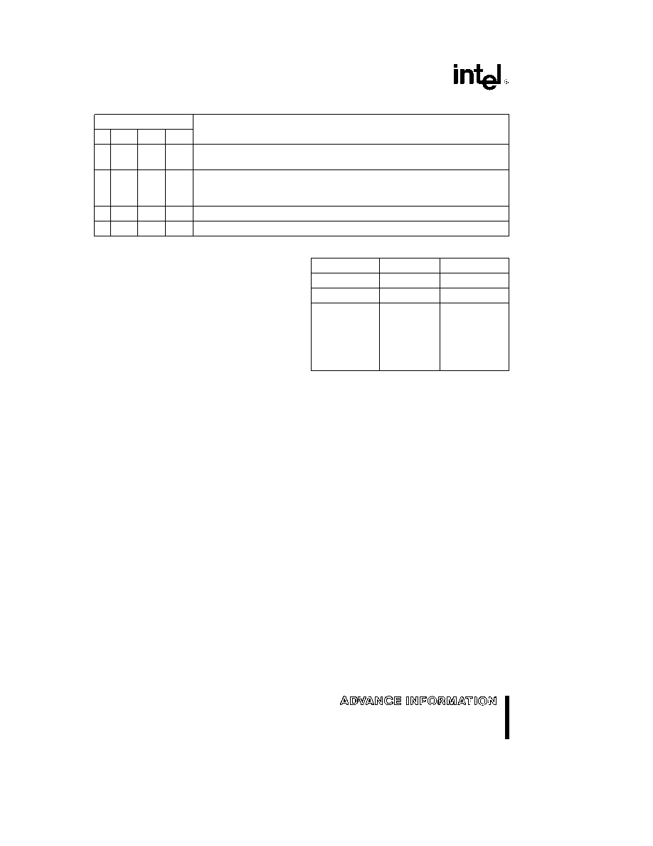
Table 3 OTP ROM Programming Modes
(H e 2 7V to 3 6V H1 e 5V
g
10%)
Mode
RST
PSEN
ALE
EA
P2 6
P2 7
P3 3
P3 6
P3 7
V
CC
PROG
V
PP
Program Code Data
H1
L
12 75V
L
H1
H1
H1
H1
H1
Verify Code Data
H
L
H
H
L
L
L
H
H
H
Program Encryption
H1
L
12 75V
L
H1
H1
L
H1
H1
Array Address 0 ≠ 3FH
Program Lock
Bit 1
H1
L
12 75V
H1
H1
H1
H1
H1
H1
Bits
Bit 2
H1
L
12 75V
H1
H1
H1
L
L
H1
Bit 3
H1
L
12 75V
H1
L
H1
H1
L
H1
Read Signature Byte
H
L
H
H
L
L
L
L
L
H
272468 ≠ 18
See Table 2 for proper input on these pins
Figure 10 Programming the OTP ROM
16
8XL52 54 58
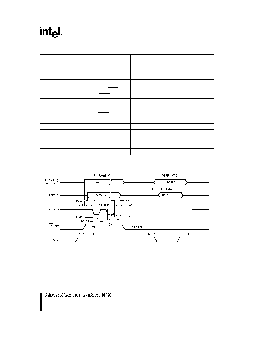
PROGRAMMING ALGORITHM
Refer to Table 3 and Figures 10 and 11 for address
data and control signals set up To program the
87L5X the following sequence must be exercised
1 Input the valid address on the address lines
2 Input the appropriate data byte on the data
lines
3 Activate the correct combination of control sig-
nals
4 Raise EA V
PP
from V
CC
to 12 75V
g
0 25V
5 Pulse ALE PROG 5 times for the OTP ROM
array and 25 times for the encryption table and
the lock bits
Repeat 1 through 5 changing the address and data
for the entire array or until the end of the object file is
reached
PROGRAM VERIFY
Program verify may be done after each byte or block
of bytes is programmed In either case a complete
verify of the programmed array will ensure reliable
programming of the 8XL5X
The lock bits cannot be directly verified Verification
of the lock bits is done by observing that their fea-
tures are enabled
272468 ≠ 19
Figure 11 Programming Signals Waveforms
ROM and OTP ROM Lock System
The 87L5X program lock system
when pro-
grammed protects the onboard program against
software piracy
The 80L5X has a one-level program lock system and
a 64-byte encryption table See line 2 of Table 4 If
program protection is desired the user submits the
encryption table with their code and both the lock-
bit and encryption array are programmed by the fac-
tory The encryption array is not available without
the lock bit For the lock bit to be programmed the
user must submit an encryption table
The 87L5X has a 3-level program lock system and a
64-byte encryption array Since this is an OTP ROM
device all locations are user-programmable See
Table 4
Encryption Array
Within the OTP ROM array are 64 bytes of Encryp-
tion Array that are initially unprogrammed (all 1's)
Every time that a byte is addressed during a verify 6
address lines are used to select a byte of the En-
cryption Array This byte is then exclusive-NOR'ed
(XNOR) with the code byte creating an Encryption
Verify byte The algorithm with the array in the un-
programmed state (all 1's) will return the code in its
original unmodified form For programming the En-
cryption Array refer to Table 3 (Programming the
OTP ROM)
When using the encryption array one important fac-
tor needs to be considered If a code byte has the
value 0FFH verifying the byte will produce the en-
cryption byte value lf a large block (
l
64 bytes) of
code is left unprogrammed a verification routine will
display the contents of the encryption array For this
reason all unused code bytes should be pro-
grammed with some value other than 0FFH and not
all of them the same value This will ensure maxi-
mum program protection
17
8XL52 54 58
Table 4 Program Lock Bits and the Features
Program Lock Bits
ProtectIon Type
LB1
LB2
LB3
1
U
U
U
No Program Lock features enabled (Code verify will still be encrypted by the
Encryption Array if programmed )
2
P
U
U
MOVC instructions executed from external program memory are disabled from
fetching code bytes from internal memory EA is sampled and latched on Reset
and further programming of the OTP ROM is disabled
3
P
P
U
Same as 2 also verify is disabled
4
P
P
P
Same as 3 also external execution is disabled
Any other combination of the lock bits is not defined
Program Lock Bits
The 8XL5X has 3 programmable lock bits that when
programmed according to Table 4 will provide differ-
ent levels of protection for the on-chip code and
data
Reading the Signature Bytes
The 87L5X 80L5X has 3 signature bytes in locations
30H 31H and 60H To read these bytes follow the
procedure for OTP ROM verify but activate the con-
trol lines provided in Table 3 for Read Signature
Byte
Location
Device
Contents
30H
All
89H
31H
All
58H
60H
80L52
30
87L52
B0
80L54
31
87L54
B1
80L58
32
87L58
B2
18
8XL52 54 58
OTP ROM PROGRAMMING AND VERIFICATION CHARACTERISTICS
(T
A
e
21 C to 27 C V
CC
e
2 7V to 3 6V V
SS
e
0V)
Symbol
Parameter
Min
Max
Units
V
PP
Programming Supply Voltage
12 5
13 0
V
I
PP
Programming Supply Current
75
mA
1 TCLCL
Oscillator Frequency
4
6
MHz
TAVGL
Address Setup to PROG Low
48TCLCL
TGHAX
Address Hold after PROG
48TCLCL
TDVGL
Data Setup to PROG Low
48TCLCL
TGHDX
Data Hold after PROG
48TCLCL
TEHSH
P2 7 (ENABLE) High to V
PP
48TCLCL
TSHGL
V
PP
Setup to PROG Low
10
m
s
TGHSL
V
PP
Hold after PROG
10
m
s
TGLGH
PROG Width
90
100
m
s
TAVQV
Address to Data Valid
48TCLCL
TELQV
ENABLE Low to Data Valid
48TCLCL
TEHQZ
Data Float after ENABLE
0
48TCLCL
TGHGL
PROG High to PROG Low
10
m
s
OTP ROM PROGRAMMING AND VERIFICATION WAVEFORMS
272468 ≠ 20
NOTE
5 pulses for the OTP ROM array 25 pulses for the encryption table and lock bits
19
8XL52 54 58
Thermal Impedance
All thermal impedance data is approximate for static
air conditions at 1W of power dissipation Values will
change depending on operating conditions and ap-
plications See the Intel Packaging Handbook (Order
Number 240800) for a description of Intel's thermal
impedance test methodology
Package
i
JA
i
JC
Device
N
46 C W
16 C W
All
S
87 C W
18 C W
52
96 C W
24 C W
54
90 C W
22 C W
58
DATA SHEET REVISION HISTORY
This is the first issue of this data sheet
20