 | –≠–ª–µ–∫—Ç—Ä–æ–Ω–Ω—ã–π –∫–æ–º–ø–æ–Ω–µ–Ω—Ç: 8XC251TA | –°–∫–∞—á–∞—Ç—å:  PDF PDF  ZIP ZIP |

© INTEL CORPORATION, 1997
November, 1997
Order Number: 273129-001
ADVANCE INFORMATION
8xC251TA/TB/TP/TQ
HIGH-PERFORMANCE CHMOS MICROCONTROLLER
Commercial/Express
s
Real-time and Programmed Wait State
Bus Operation
s
Binary-code Compatible with MCS
Æ
51
s
Pin Compatible with 44-pin PLCC and
40-pin PDIP MCS 51 Sockets
s
Register-based MCS
Æ
251 Architecture
-- 40-byte Register File
-- Registers Accessible as Bytes,
Words, or Double Words
s
Enriched MCS 51 Instruction Set
-- 16-bit and 32-bit Arithmetic and
Logic Instructions
-- Compare and Conditional Jump
Instructions
-- Expanded Set of Move Instructions
s
Linear Addressing
s
256-Kbyte Expanded External
Code/Data Memory Space
s
ROM Options:
16 Kbytes (TB/TQ), 8 Kbytes (TA/TP), or
without ROM
s
16-bit Internal Code Fetch
s
64-Kbyte Extended Stack Space
s
On-chip Data RAM Options:
1-Kbyte (TA/TB) or 512-Byte (TP/TQ)
s
8-bit, 2-clock External Code Fetch in
Page Mode
s
Fast MCS 251 Instruction Pipeline
s
User-selectable Configurations:
-- External Wait States (0-3 wait
states)
-- Address Range & Memory Mapping
-- Page Mode
-- Extended Data Float Timings or
8xC251Sx Compatible AC Timings
s
32 Programmable I/O Lines
s
Eight Maskable Interrupt Sources with
Four Programmable Priority Levels
s
Three Flexible 16-bit Timer/counters
s
Hardware Watchdog Timer
s
Programmable Counter Array
-- High-speed Output
-- Compare/Capture Operation
-- Pulse Width Modulator
-- Watchdog Timer
s
Two Programmable Serial I/O Ports
-- Framing Error Detection
-- Automatic Address Recognition
s
High-performance CHMOS Technology
s
Static Standby to 24-MHz Operation
s
Complete System Development
Support
-- Compatible with Existing Tools
-- MCS 251 Tools Available:
Compiler, Assembler, Debugger,
ICE
s
Package Options (PDIP and PLCC)

Information in this document is provided in connection with Intel products. No license, express or implied, by
estoppel or otherwise, to any intellectual property rights is granted by this document. Except as provided in
Intel's Terms and Conditions of Sale for such products, Intel assumes no liability whatsoever, and Intel
disclaims any express or implied warranty, relating to sale and/or use of Intel products including liability or
warranties relating to fitness for a particular purpose, merchantability, or infringement of any patent, copyright
or other intellectual property right. Intel products are not intended for use in medical, life saving, or life
sustaining applications. Intel may make changes to specifications and product descriptions at any time, without
notice. Contact your local Intel sales office or your distributor to obtain the latest specifications and before
placing your product order.
Designers must not rely on the absence or characteristics of any features or instructions marked "reserved" or
"undefined." Intel reserves these for future definition and shall have no responsibility whatsoever for conflicts or
incompatibilities arising from future changes to them.
The 8xC251TA/TB/TP/TQ may contain design defects or errors known as errata which may cause the product
to deviate from published specifications. Current characterized errata are available on request.
Copies of documents which have an ordering number and are referenced in this document, or other Intel
literature, may be obtained from:
Intel Corporation
P.O. Box 5937
Denver CO 80217-9808
or call 1-800-548-4725.
Many documents are available for download from Intel's website at http://www.intel.com.
Copyright © Intel Corporation 1997.
*Third party brands and names are the property of their respective owners.

Contents
ADVANCE INFORMATION
iii
8xC251TA/TB/TP/TQ
HIGH-PERFORMANCE CHMOS Microcontroller
Commercial/Express
1.0 INTRODUCTION ......................................................................................................................................... 1
2.0 NOMENCLATURE ...................................................................................................................................... 2
3.0 PINOUT ....................................................................................................................................................... 4
4.0 SIGNALS ..................................................................................................................................................... 8
5.0 ADDRESS MAP ........................................................................................................................................ 11
6.0 ELECTRICAL CHARACTERISTICS ......................................................................................................... 12
6.1 D.C. Characteristics ........................................................................................................................... 12
6.2 Definition of AC Symbols ................................................................................................................... 14
6.3 A.C. Characteristics ........................................................................................................................... 14
6.3.1 External Bus Cycles, Nonpage Mode ..................................................................................... 18
6.3.2 External Bus Cycles, Page Mode ........................................................................................... 21
6.3.3 Definition of Real-Time Wait Symbols .................................................................................... 24
6.3.4 External Bus Cycles, Real-Time Wait States .......................................................................... 24
6.4 AC Characteristics -- Serial Port, Shift Register Mode ..................................................................... 28
6.5 External Clock Drive .......................................................................................................................... 29
7.0 THERMAL CHARACTERISTICS .............................................................................................................. 30

Contents
iv
ADVANCE INFORMATION
FIGURES
Figure 1.
8xC251TA/TB/TP/TQ Block Diagram ........................................................................................ 1
Figure 2.
The 8xC251TA/TB/TP/TQ Family Nomenclature....................................................................... 2
Figure 3.
8xC251TA/TB/TP/TQ 44-pin PLCC Package ............................................................................ 4
Figure 4.
8xC251TA/TB/TP/TQ 40-pin PDIP Packages............................................................................ 5
Figure 5.
External Bus Cycle: Code Fetch (Nonpage Mode) .................................................................. 18
Figure 6.
External Bus Cycle: Data Read (Nonpage Mode) ................................................................... 19
Figure 7.
External Bus Cycle: Data Write (Nonpage Mode).................................................................... 20
Figure 8.
External Bus Cycle: Code Fetch (Page Mode) ........................................................................ 21
Figure 9.
External Bus Cycle: Data Read (Page Mode).......................................................................... 22
Figure 10.
External Bus Cycle: Data Write (Page Mode).......................................................................... 23
Figure 11.
External Bus Cycle: Code Fetch/Data Read (Nonpage Mode)................................................ 24
Figure 12.
External Bus Cycle: Data Write (Nonpage Mode).................................................................... 25
Figure 13.
External Bus Cycle: Code Fetch/Data Read (Page Mode) ...................................................... 26
Figure 14.
External Bus Cycle: Data Write (Page Mode).......................................................................... 27
Figure 15.
Serial Port Waveform -- Shift Register Mode.......................................................................... 28
Figure 16.
External Clock Drive Waveforms ............................................................................................. 29
Figure 17.
AC Testing Input, Output Waveforms ...................................................................................... 29
Figure 18.
Float Waveforms...................................................................................................................... 30
TABLES
Table 1.
Description of Product Nomenclature ........................................................................................ 2
Table 2.
Proliferation Options .................................................................................................................. 3
Table 3.
Package Information .................................................................................................................. 3
Table 4.
8xC251TA/TB/TP/TQ Pin Assignment ....................................................................................... 6
Table 5.
8xC251TA/TB/TP/TQ PLCC/DIP Pin Assignments Arranged by Functional Category .............. 7
Table 6.
Signal Descriptions .................................................................................................................... 8
Table 7.
Memory Signal Selections (RD1:0) .......................................................................................... 10
Table 8.
8xC251TA/TB/TP/TQ Address Map ......................................................................................... 11
Table 9.
DC Characteristics at V
CC
= 4.5 ≠ 5.5 V .................................................................................. 12
Table 10.
AC Timing Symbol Definitions ................................................................................................. 14
Table 11.
AC Characteristics ................................................................................................................... 14
Table 12.
Real-time Wait Timing Symbol Definitions ............................................................................... 24
Table 13.
Real-Time Wait AC Timing ...................................................................................................... 27
Table 14.
Serial Port Timing -- Shift Register Mode ............................................................................... 28
Table 15.
External Clock Drive ................................................................................................................ 29
Table 16.
Thermal Characteristics ........................................................................................................... 30
ADVANCE INFORMATION
1
8xC251TA/TB/TP/TQ HIGH-PERFORMANCE CHMOS MICROCONTROLLER
1.0
INTRODUCTION
A member of the Intel family of 8-bit MCS 251 micro-
controllers, the 8xC251TA/TB/TP/TQ is binary-code
compatible with MCS 51 microcontrollers and pin
compatible with 40-pin PDIP and 44-pin PLCC
MCS 51 microcontrollers. MCS 251 microcontrollers
feature an enriched instruction set, linear
addressing, and efficient C-language support. The
8xC251TA/TB/TP/TQ has 512 bytes or 1 Kbyte of
on-chip RAM and is available with 8 Kbytes or 16
Kbytes of on-chip ROM, or without ROM. A variety of
features can be selected by new user-programmable
configurations.
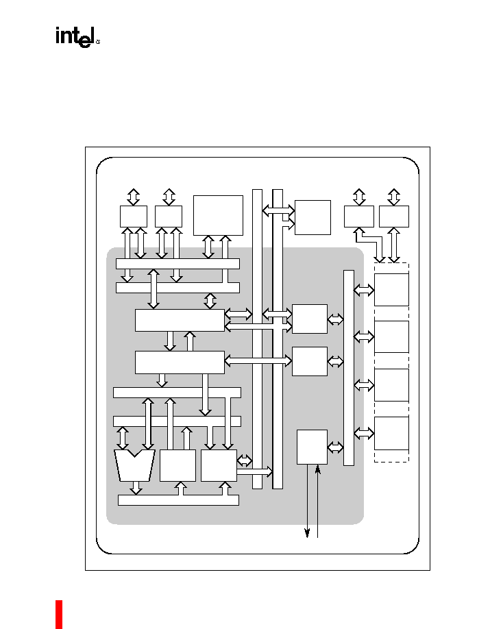
Figure 1. 8xC251TA/TB/TP/TQ Block Diagram
A4530-01
SRC2 (8)
Code Address (24)
Clock & Reset
Code Bus (16)
Data RAM
512 Bytes
or
1024 Bytes
Code
OTPROM/ROM
8 Kbytes
or
16 Kbytes
Watchdog
Timer
Timer/
Counters
PCA
Two
Serial I/O
Ports
Peripherals
Port 2
Drivers
P2.7:0
Port 0
Drivers
P0.7:0
Port 3
Drivers
P3.7:0
Port 1
Drivers
P1.7:0
Data Address (24)
Data Bus (8)
Memory Address (16)
MCS
Æ
251 Microcontroller Core
System Bus and I/O Ports
I/O Ports and
Peripheral Signals
SRC1 (8)
IB Bus (8)
Peripheral
Interface
Interrupt
Handler
Clock
&
Reset
Bus Interface
Instruction Sequencer
DST (16)
ALU
Data
Memory
Interface
Memory Data (16)
Register
File
8XC251TA/TB/TP/TQ Microcontroller
8xC251TA/TB/TP/TQ HIGH-PERFORMANCE CHMOS MICROCONTROLLER
2
ADVANCE INFORMATION
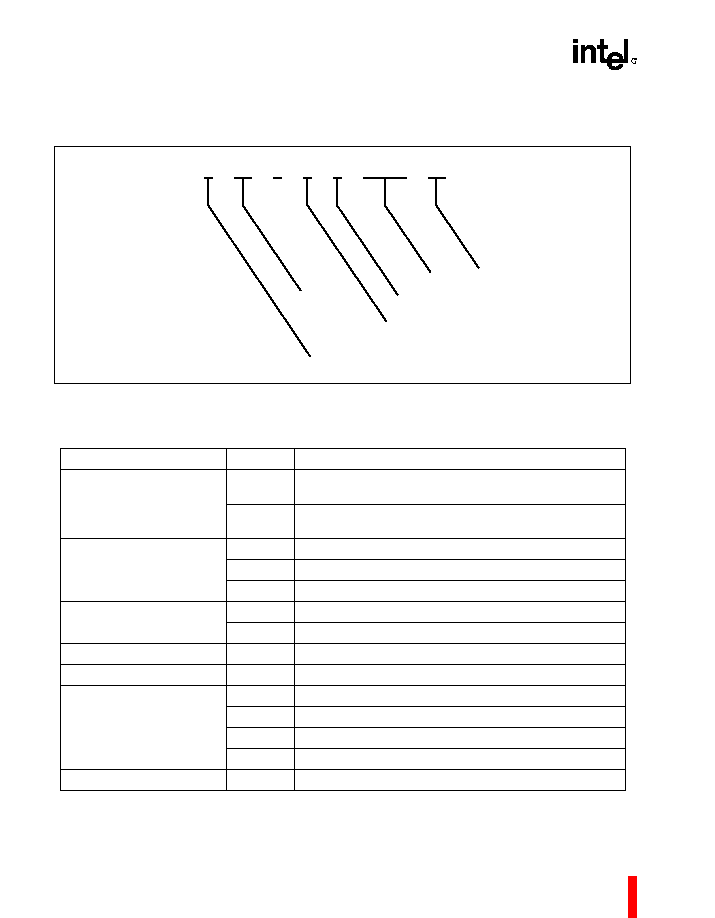
2.0
NOMENCLATURE
Figure 2. The 8xC251TA/TB/TP/TQ Family Nomenclature
Table 1. Description of Product Nomenclature
Parameter
Options
Description
Temperature and Burn-in
Options
no mark
Commercial operating temperature range (0∞C to 70∞C) with
Intel standard burn-in.
T
Express operating temperature range (-40∞C to 85∞C)
without Intel standard burn-in.
Packaging Options
N
44-pin Plastic Leaded Chip Carrier (PLCC)
P
40-pin Plastic Dual In-line Package (PDIP)
C
40-pin Ceramic Dual In-line Package (Ceramic DIP)
Program Memory Options
0
Without ROM
3
ROM
Process Information
C
CHMOS
Product Family
251
8-bit control architecture
Device Memory Options
TA
1-Kbyte RAM/8-Kbyte ROM
TB
1-Kbyte RAM/16-Kbyte ROM or without ROM
TP
512-byte RAM/8-Kbyte ROM
TQ
512-byte RAM/16-Kbyte ROM or without ROM
Device Speed
24
External clock frequency
Program-memory Options
XXXXX
XX
X
X
8
XX
X
Packaging Options
Temperature and Burn-in Options
A2815-01
Process Information
Product Family Device Speed
8xC251TA/TB/TP/TQ HIGH-PERFORMANCE CHMOS MICROCONTROLLER
ADVANCE INFORMATION
3
Table 2
lists the proliferation options. See
Figure 2
for the 8xC251TA/TB/TP/TQ family nomenclature.
Table
lists the 8xC251TA/TB/TP/TQ package definitions.
Table 2. Proliferation Options
8xC251TA/TB/TP/TQ
(0 ≠ 24 MHz; 5 V ±10%)
80C251TB24
CPU-only
80C251TQ24
CPU-only
83C251TA24
ROM
83C251TB24
ROM
83C251TP24
ROM
83C251TQ24
ROM
Table 3. Package Information
Pkg.
Definition
Temperature
N
44 ld. PLCC
0∞C to +70∞C
P
40 ld. Plastic DIP
0∞C to +70∞C
TN
44 ld. PLCC
-40∞C to +85∞C
TP
40 ld. Plastic DIP
-40∞C to +85∞C
8xC251TA/TB/TP/TQ HIGH-PERFORMANCE CHMOS MICROCONTROLLER
4
ADVANCE INFORMATION
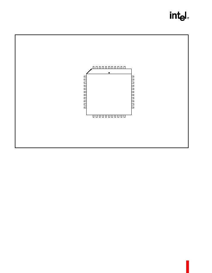
3.0
PINOUT
Figure 3. 8xC251TA/TB/TP/TQ 44-pin PLCC Package
A4538-01
AD4 / P0.4
AD5 / P0.5
AD6 / P0.6
AD7 / P0.7
EA#
V
SS2
ALE
PSEN#
A15 / P2.7
A14 / P2.6
A13 / P2.5
P1.4 / CEX1
P1.3 / CEX0 / TXD1
P1.2 / ECI / RXD1
P1.1 / T2EX
P1.0 /
T2
V
SS1
V
CC
AD0 / P0.0
AD1 / P0.1
AD2 / P0.2
AD3 / P0.3
P1.5 / CEX2
P1.6 / CEX3 / WAIT#
P1.7 / CEX4 / A17 / WCLK
RST
P3.0 / RXD
V
CC2
P3.1 / TXD
P3.2 / INT0#
P3.3 / INT1#
P3.4 / T0
P3.5 / T1
39
38
37
36
35
34
33
32
31
30
29
8XC251TA
8XC251TB
8XC251TP
8XC251TQ
View of component as
mounted on PC board
7
8
9
10
11
12
13
14
15
16
17
P3.6 / WR#
P3.7 / RD# / A16
XTAL2
XTAL1
V
SS
V
SS2
A8 / P2.0
A9 / P2.1
A10 / P2.2
A11 / P2.3
A12 / P2.4
18
19
20
21
22
23
24
25
26
27
28
6
5
4
3
2
1
44
43
42
41
40
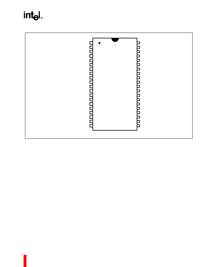
8xC251TA/TB/TP/TQ HIGH-PERFORMANCE CHMOS MICROCONTROLLER
ADVANCE INFORMATION
5
Figure 4. 8xC251TA/TB/TP/TQ 40-pin PDIP Packages
A4532-02
1
2
3
4
5
6
7
8
9
10
11
12
13
14
15
16
17
18
19
20
V
CC
AD0 / P0.0
AD1 / P0.1
AD2 / P0.2
AD3 / P0.3
AD4 / P0.4
AD5 / P0.5
AD6 / P0.6
AD7 / P0.7
EA#
ALE
PSEN#
A15 / P2.7
A14 / P2.6
A13 / P2.5
A12 / P2.4
A11 / P2.3
A10 / P2.2
A9 / P2.1
A8 / P2.0
P1.0 / T2
P1.1 / T2EX
P1.2 / ECI / RXD1
P1.3 / CEX0 / TXD1
P1.4 / CEX1
P1.5 / CEX2
P1.6 / CEX3 / WAIT#
P1.7 / CEX4 / A17 / WCLK
RST
P3.0 / RXD
P3.1 / TXD
P3.2 / INT0#
P3.3 / INT1#
P3.4 / T0
P3.5 / T1
P3.6 / WR#
P3.7 / RD# / A16
XTAL2
XTAL1
V
SS
40
39
38
37
36
35
34
33
32
31
30
29
28
27
26
25
24
23
22
21
8XC251TA
8XC251TB
8XC251TP
8XC251TQ
View of
component
as mounted
on PC board
8xC251TA/TB/TP/TQ HIGH-PERFORMANCE CHMOS MICROCONTROLLER
6
ADVANCE INFORMATION
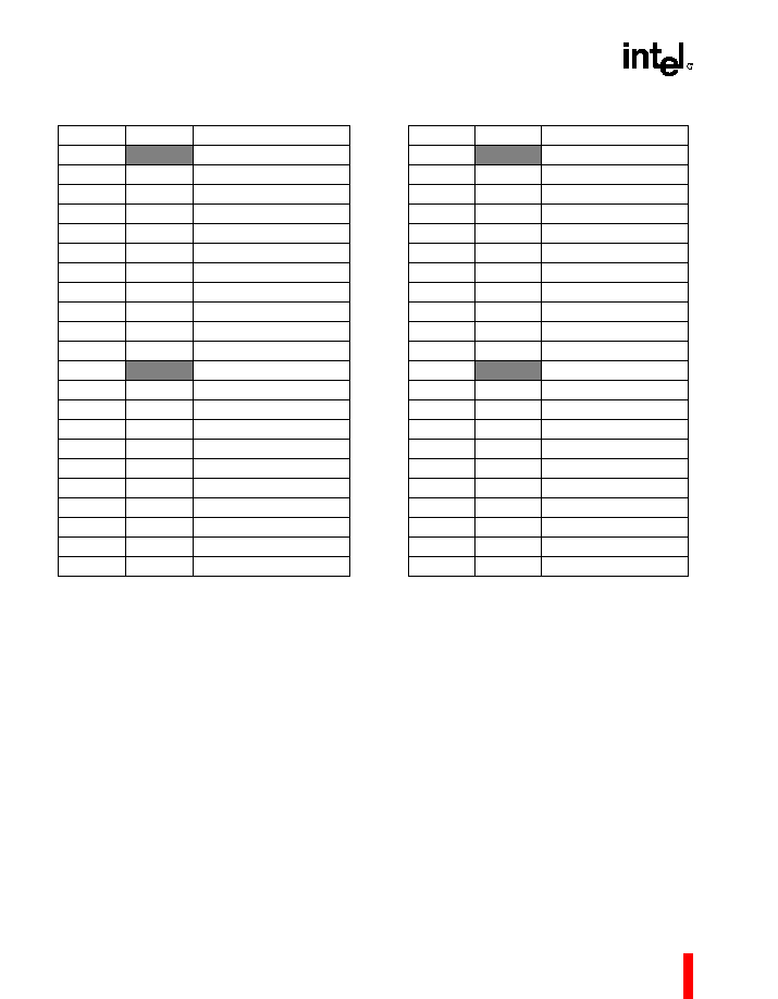
Table 4. 8xC251TA/TB/TP/TQ Pin Assignment
PLCC
DIP
Name
PLCC
DIP
Name
1
V
SS1
23
V
SS2
2
1
P1.0/T2
24
21
A8/P2.0
3
2
P1.1/T2EX
25
22
A9/P2.1
4
3
P1.2/ECI/RXD1
26
23
A10/P2.2
5
4
P1.3/CEX0/TXD1
27
24
A11/P2.3
6
5
P1.4/CEX1
28
25
A12/P2.4
7
6
P1.5/CEX2
29
26
A13/P2.5
8
7
P1.6/CEX3/WAIT#
30
27
A14/P2.6
9
8
P1.7/CEX4/A17/WCLK
31
28
A15/P2.7
10
9
RST
32
29
PSEN#
11
10
P3.0/RXD
33
30
ALE
12
V
CC2
34
V
SS2
13
11
P3.1/TXD
35
31
EA#
14
12
P3.2/INT0#
36
32
AD7/P0.7
15
13
P3.3/INT1#
37
33
AD6/P0.6
16
14
P3.4/T0
38
34
AD5/P0.5
17
15
P3.5/T1
39
35
AD4/P0.4
18
16
P3.6/WR#
40
36
AD3/P0.3
19
17
P3.7/RD#/A16
41
37
AD2/P0.2
20
18
XTAL2
42
38
AD1/P0.1
21
19
XTAL1
43
39
AD0/P0.0
22
20
V
SS
44
40
V
CC
8xC251TA/TB/TP/TQ HIGH-PERFORMANCE CHMOS MICROCONTROLLER
ADVANCE INFORMATION
7
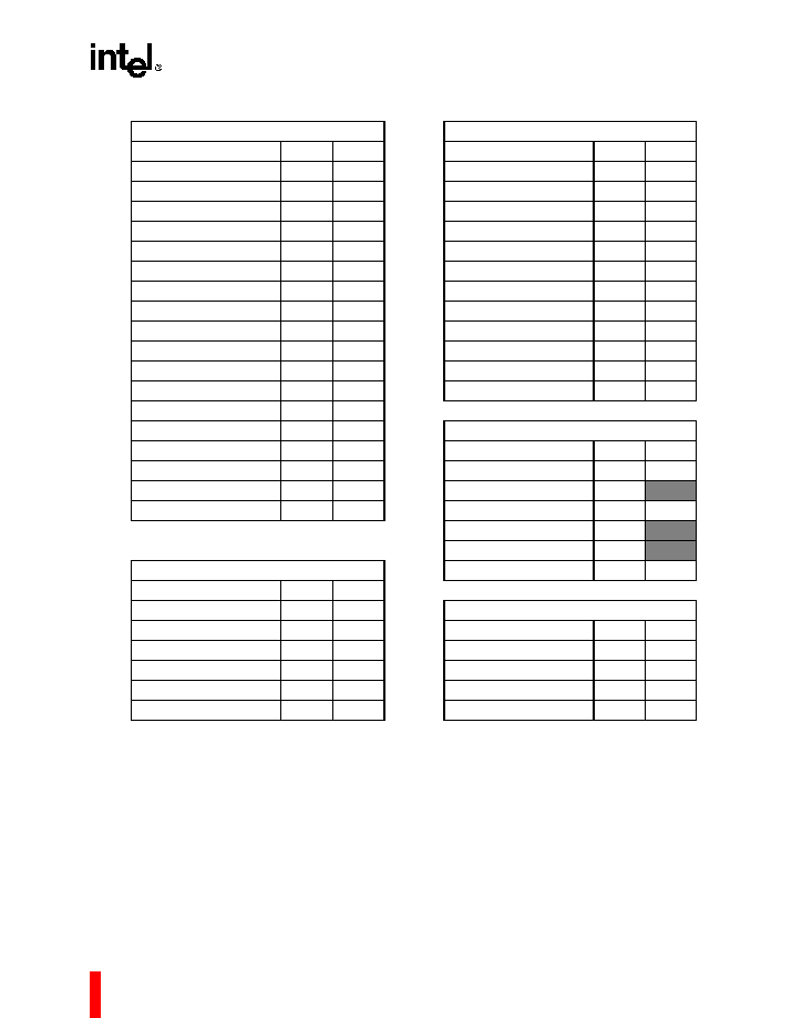
Table 5. 8xC251TA/TB/TP/TQ PLCC/DIP Pin Assignments Arranged by Functional Category
Address & Data
Input/Output
Name
PLCC
DIP
Name
PLCC
DIP
AD0/P0.0
43
39
P1.0/T2
2
1
AD1/P0.1
42
38
P1.1/T2EX
3
2
AD2/P0.2
41
37
P1.2/ECI/RXD1
4
3
AD3/P0.3
40
36
P1.3/CEX0/TXD1
5
4
AD4/P0.4
39
35
P1.4/CEX1
6
5
AD5/P0.5
38
34
P1.5/CEX2
7
6
AD6/P0.6
37
33
P1.6/CEX3/WAIT#
8
7
AD7/P0.7
36
32
P1.7/CEX4/A17/WCLK
9
8
A8/P2.0
24
21
P3.0/RXD
11
10
A9/P2.1
25
22
P3.1/TXD
13
11
A10/P2.2
26
23
P3.4/T0
16
14
A11/P2.3
27
24
P3.5/T1
17
15
A12/P2.4
28
25
A13/P2.5
29
26
Power & Ground
A14/P2.6
30
27
Name
PLCC
DIP
A15/P2.7
31
28
V
CC
44
40
P3.7/RD#/A16
19
17
V
CC2
12
P1.7/CEX4/A17/WCLK
9
8
V
SS
22
20
V
SS1
1
V
SS2
23, 34
Processor Control
EA#
35
31
Name
PLCC
DIP
P3.2/INT0#
14
12
Bus Control & Status
P3.3/INT1#
15
13
Name
PLCC
DIP
EA#
35
31
P3.6/WR#
18
16
RST
10
9
P3.7/RD#/A16
19
17
XTAL1
21
18
ALE
33
30
XTAL2
20
19
PSEN#
32
29
8xC251TA/TB/TP/TQ HIGH-PERFORMANCE CHMOS MICROCONTROLLER
8
ADVANCE INFORMATION
4.0
SIGNALS
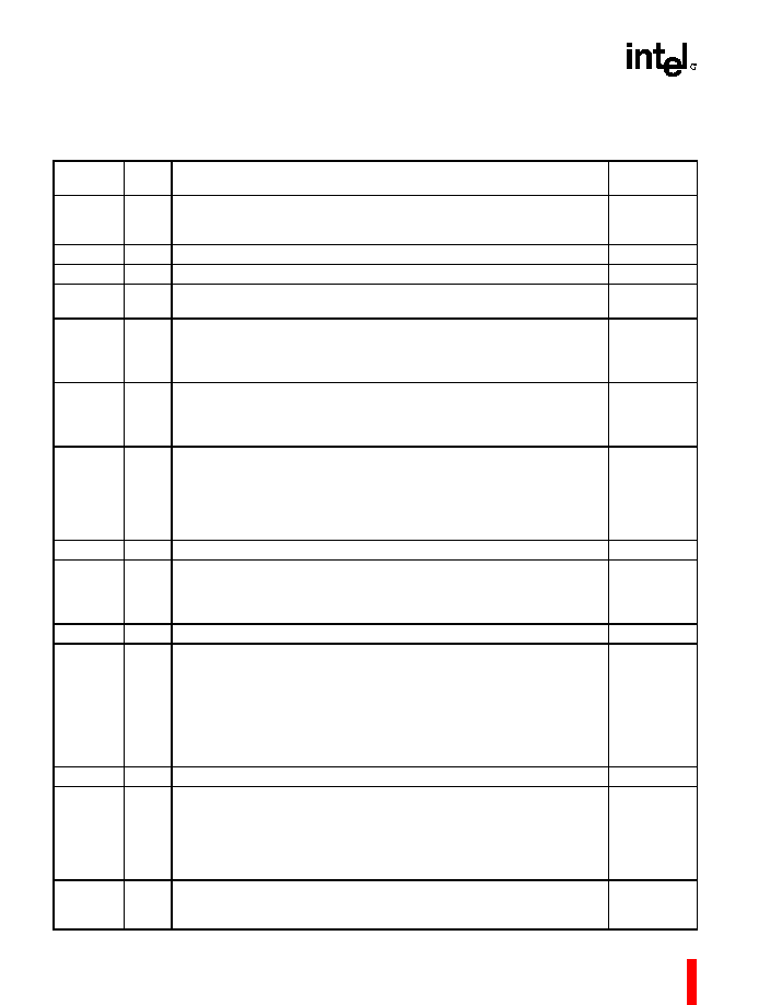
Table 6. Signal Descriptions (Sheet 1 of 3)
Signal
Name
Type
Description
Alternate
Function
A17
O
18th Address Bit (A17). Output to memory as 18th external address bit
(A17) in extended bus applications, depending on the values of bits RD0
and RD1 in configuration byte UCONFIG0. See also RD# and PSEN#.
P1.7/CEX4/
WCLK
A16
O
Address Line 16. See RD#.
RD#
A15:8
1
O
Address Lines. Upper address lines for the external bus.
P2.7:0
AD7:0
1
I/O
Address/Data Lines. Multiplexed lower address lines and data lines for
external memory.
P0.7:0
ALE
O
Address Latch Enable. ALE signals the start of an external bus cycle
and indicates that valid address information is available on lines A15:8
and AD7:0. An external latch can use ALE to demultiplex the address
from the address/data bus.
CEX4:0
I/O
Programmable Counter Array (PCA) Input/Output Pins. These are
input signals for the PCA capture mode and output signals for the PCA
compare mode and PCA PWM mode.
P1.6:4
P1.7/A17/
WAIT#
P1.3/TXD1
EA#
I
External Access. Directs program memory accesses to on-chip or off-
chip code memory. For EA# = 0, all program memory accesses are off-
chip. For EA# = 1, an access is to on-chip ROM if the address is within
the range of the on-chip ROM; otherwise the access is off-chip. The value
of EA# is latched at reset. For devices without on-chip ROM, EA# must
be strapped to ground.
ECI
I
PCA External Clock Input. External clock input to the 16-bit PCA timer.
P1.2/RXD1
INT1:0#
I
External Interrupts 0 and 1. These inputs set bits IE1:0 in the TCON
register. If bits IT1:0 in the TCON register are set, bits IE1:0 are set by a
falling edge on INT1#/INT0#. If bits INT1:0 are clear, bits IE1:0 are set by
a low level on INT1:0#.
P3.3:2
P0.7:0
I/O
Port 0. This is an 8-bit, open-drain, bidirectional I/O port.
AD7:0
P1.0
P1.1
P1.2
P1.7:3
I/O
Port 1. This is an 8-bit, bidirectional I/O port with internal pullups.
T2
T2EX
ECI/RXD1
CEX3:1
CEX4/A17/
WAIT#/
WCLK
CEX0/TXD1
P2.7:0
I/O
Port 2. This is an 8-bit, bidirectional I/O port with internal pullups.
A15:8
P3.0
P3.1
P3.3:2
P3.5:4
P3.6
P3.7
I/O
Port 3. This is an 8-bit, bidirectional I/O port with internal pullups.
RXD
TXD
INT1:0#
T1:0
WR#
RD#/A16
PSEN#
O
Program Store Enable. Read signal output. This output is asserted for a
memory address range that depends on bits RD0 and RD1 in configu-
ration byte UCONFIG0 (see RD#).
--
8xC251TA/TB/TP/TQ HIGH-PERFORMANCE CHMOS MICROCONTROLLER
ADVANCE INFORMATION
9
RD#
O
Read or 17th Address Bit (A16). Read signal output to external data
memory or 17th external address bit (A16), depending on the values of
bits RD0 and RD1 in configuration byte UCONFIG0. (See PSEN#).
P3.7/A16
RST
I
Reset. Reset input to the chip. Holding this pin high for 64 oscillator
periods while the oscillator is running resets the device. The port pins are
driven to their reset conditions when a voltage greater than V
IH1
is
applied, whether or not the oscillator is running. This pin has an internal
pulldown resistor, which allows the device to be reset by connecting a
capacitor between this pin and V
CC
.
Asserting RST when the chip is in idle mode or powerdown mode returns
the chip to normal operation.
--
RXD
I/O
Receive Serial Data. RXD sends and receives data in serial I/O mode 0
and receives data in serial I/O modes 1, 2, and 3.
P3.0
RXD1
I/O
Receive Serial Data 1. RXD1 sends and receives data in serial I/O
mode 0 and receives data in serial I/O modes 1, 2, and 3 for the 2nd
serial port.
P1.2/ECI
T1:0
I
Timer 1:0 External Clock Inputs. When timer 1:0 operates as a counter,
a falling edge on the T1:0 pin increments the count.
P3.5:4
T2
I/O
Timer 2 Clock Input/Output. For the timer 2 capture mode, this signal is
the external clock input. For the clock-out mode, it is the timer 2 clock
output.
P1.0
T2EX
I
Timer 2 External Input. In timer 2 capture mode, a falling edge initiates a
capture of the timer 2 registers. In auto-reload mode, a falling edge
causes the timer 2 registers to be reloaded. In the up-down counter
mode, this signal determines the count direction: 1 = up, 0 = down.
P1.1
TXD
O
Transmit Serial Data. TXD outputs the shift clock in serial I/O mode 0
and transmits serial data in serial I/O modes 1, 2, and 3.
P3.1
TXD1
O
Transmit Serial Data 1. TXD1 outputs the shift clock in serial I/O mode 0
and transmits serial data in serial I/O modes 1, 2, and 3 for the 2nd serial
port.
P1.3/CEX0
V
CC
PWR
Supply Voltage. Connect this pin to the +5V supply voltage.
--
V
CC2
PWR
Secondary Supply Voltage 2. This supply voltage connection is
provided to reduce power supply noise. Connection of this pin to the +5V
supply voltage is recommended. However, when using the 8XC251SB as
a pin-for-pin replacement for the 8XC51FX, V
SS
2
can be unconnected
without loss of compatibility. (Not available on DIP)
--
V
SS
GND
Circuit Ground. Connect this pin to ground.
--
V
SS1
GND
Secondary Ground. This ground is provided to reduce ground bounce
and improve power supply bypassing. Connection of this pin to ground is
recommended. However, when using the 8xC251TA/TB/TP/TQ as a pin-
for-pin replacement for the 8XC51BH, V
SS1
can be unconnected without
loss of compatibility. (Not available on DIP)
--
V
SS2
GND
Secondary Ground 2. This ground is provided to reduce ground bounce
and improve power supply bypassing. Connection of this pin to ground is
recommended. However, when using the 8xC251TA/TB/TP/TQ as a pin-
for-pin replacement for the 8XC51FX, V
SS2
can be unconnected without
loss of compatibility. (Not available on DIP)
--
Table 6. Signal Descriptions (Sheet 2 of 3)
Signal
Name
Type
Description
Alternate
Function
8xC251TA/TB/TP/TQ HIGH-PERFORMANCE CHMOS MICROCONTROLLER
10
ADVANCE INFORMATION
WAIT#
I
Real-time Wait State Input. The real-time WAIT# input is enabled by
writing a logical `1' to the WCON.0 (RTWE) bit at S:A7H. During bus
cycles, the external memory system can signal `system ready' to the
microcontroller in real time by controlling the WAIT# input signal on the
port 1.6 input.
P1.6/CEX3
WCLK
O
Wait Clock Output. The real-time WCLK output is driven at port 1.7
(WCLK) by writing a logical `1' to the WCON.1 (RTWCE) bit at S:A7H.
When enabled, the WCLK output produces a square wave signal with a
period of one-half the oscillator frequency.
P1.7/CEX4/
A17
WR#
O
Write. Write signal output to external memory.
P3.6
XTAL1
I
Input to the On-chip, Inverting, Oscillator Amplifier. To use the
internal oscillator, a crystal/resonator circuit is connected to this pin. If an
external oscillator is used, its output is connected to this pin. XTAL1 is the
clock source for internal timing.
--
XTAL2
O
Output of the On-chip, Inverting, Oscillator Amplifier. To use the
internal oscillator, a crystal/resonator circuit is connected to this pin. If an
external oscillator is used, leave XTAL2 unconnected.
--
NOTE:
The descriptions of A15:8/P2.7:0 and AD7:0/P0.7:0 are for the nonpage-mode chip configuration (compatible with 44-pin
PLCC and 40-pin DIP MCS 51 microcontrollers). If the chip is configured for page-mode operation, port 0 carries the lower
address bits (A7:0), and port 2 carries the upper address bits (A15:8) and the data (D7:0).
Table 7. Memory Signal Selections (RD1:0)
RD1:0
P1.7/CEX/
A17/WCLK
P3.7/RD#/A16
PSEN#
WR#
Features
0 0
A17
A16
Asserted for all
addresses
Asserted for writes to
all memory locations
256-Kbyte external
memory
0 1
P1.7/CEX4/
WCLK
A16
Asserted for all
addresses
Asserted for writes to
all memory locations
128-Kbyte external
memory
1 0
P1.7/CEX4/
WCLK
P3.7 only
Asserted for all
addresses
Asserted for writes to
all memory locations
64-Kbyte external
memory. One
additional port pin.
1 1
P1.7/CEX4/
WCLK
RD# asserted
for addresses
7F:FFFFH
Asserted for
80:0000H
Asserted only for
writes to MCS 51
microcontroller data
memory
locations.
64-Kbyte external
memory. Compatible
with MCS 51 micro-
controllers.
Table 6. Signal Descriptions (Sheet 3 of 3)
Signal
Name
Type
Description
Alternate
Function
8xC251TA/TB/TP/TQ HIGH-PERFORMANCE CHMOS MICROCONTROLLER
ADVANCE INFORMATION
11
5.0
ADDRESS MAP
Table 8. 8xC251TA/TB/TP/TQ Address Map
Internal
Address)
Description
Notes
FF:FFFFH
FF:4000H
External Memory except the top eight bytes (FF:FFF8H≠FF:FFFFH) which are
reserved for the configuration array.
1, 3, 10
FF:3FFFH
FF:0000H
External memory or on-chip nonvolatile memory (8Kbytes FF:0000H - FF:1FFFH,
16Kbytes FF:0000H - FF:3FFFH).
3, 4, 5
FE:FFFFH
FE:0000H
External Memory
3
FD:FFFFH
02:0000H
Reserved
6
01:FFFFH
01:0000H
External Memory
3
00:FFFFH
00:E000H
External memory or with configuration bit EMAP# = 0, addresses in this range
access on-chip code memory in region FF: (16 Kbyte devices only).
5, 7
00:DFFFH
00:0420H
External Memory
7
00:041FH
00:0080H
On-chip RAM (512 bytes 00:0020H - 00:021FH, 1024 bytes 00:0020H - 00:041FH)
7
00:007FH
00:0020H
On-chip RAM
8
00:001FH
00:0000H
Storage for R0≠R7 of Register File
2, 9
NOTES:
1. 18 address lines are bonded out (A15:0, A16:0, or A17:0 selected during chip configuration).
2. The special function registers (SFRs) and the register file have separate internal address spaces.
3. Data in this area is accessible by indirect addressing only.
4. Devices reset into internal or external starting locations depending on the state of EA# and configuration byte information
See EA#.
5. The 16-Kbyte ROM devices allow internal locations FF:2000H≠FF:3FFFH to map into region 00:. In this case, if EA# = 1,
a data read to 00:E000H≠00:FFFFH is redirected to internal ROM (see bit 1 in UCONFIG0). This is not available for 8-
Kbyte ROM devices.
6. This reserved area returns indeterminate values.
7. Data is accessible by direct and indirect addressing.
8. Data is accessible by direct, indirect, and bit addressing.
9. Data is accessible by direct, indirect, and register addressing.
10. Eight addresses at the top of all external memory maps are reserved for current and future device configuration byte
information.
8xC251TA/TB/TP/TQ HIGH-PERFORMANCE CHMOS MICROCONTROLLER
12
ADVANCE INFORMATION
6.0
ELECTRICAL CHARACTERISTICS
6.1
D.C. Characteristics
Parameter values apply to all devices unless otherwise indicated.
ABSOLUTE MAXIMUM RATINGS
Storage Temperature .................................. -65∞C to +150∞C
Voltage: EA# Pin with respect to V
SS
............. 0 V to +13.0 V
Voltage: Any other Pin with respect to V
SS
... -0.5 V to +6.5 V
I
OL
per I/O Pin............................................................... 15 mA
Power Dissipation ......................................................... 1.5 W
OPERATING CONDITIONS
T
A
(Ambient Temperature Under Bias):
Commercial ................................................. 0∞C to +70∞C
Express........................................................... -40∞C to +85∞C
V
CC
(Digital Supply Voltage) ............................ 4.5 V to 5.5 V
V
SS
................................................................................... 0 V
NOTE:Maximum power dissipation is based on
package heat-transfer limitations, not device power
consumption.
NOTICE:This document contains information on
products being sampled or in the initial production
phase of development. Verify with your local Intel
sales office that you have the latest datasheet
before finalizing a design.
WARNING
: Stressing the device beyond the
"Absolute Maximum Ratings" may cause
permanent damage. These are stress ratings only.
Operation beyond the "Operating Conditions" is not
recommended and extended exposure beyond the
"Operating Conditions" may affect device
reliability.
Table 9. DC Characteristics at V
CC
= 4.5 ≠ 5.5 V (Sheet 1 of 2)
Symbol
Parameter
Min
Typical
Max
Units
Test Conditions
V
IL
Input Low Voltage
(except EA#)
-0.5
0.2 V
CC
≠ 0.1
V
V
IL1
Input Low Voltage
(EA#)
0
0.2 V
CC
≠ 0.3
V
V
IH
Input High Voltage
(except XTAL1, RST)
0.2 V
CC
+ 0.9
V
CC
+ 0.5
V
V
IH1
Input High Voltage
(XTAL1, RST)
0.7 V
CC
V
CC
+ 0.5
V
V
OL
Output Low Voltage
(Port 1, 2, 3)
0.3
0.45
1.0
V
I
OL
= 100 µA
I
OL
= 1.6 mA
I
OL
= 3.5 mA
(Note 1, Note 2)
V
OL1
Output Low Voltage
(Port 0, ALE, PSEN#)
0.3
0.45
1.0
V
I
OL
= 200 µA
I
OL
= 3.2 mA
I
OL
= 7.0 mA
(Note 1, Note 2)
V
OH
Output High Voltage
(Port 1, 2, 3, ALE,
PSEN#)
V
CC
≠ 0.3
V
CC
≠ 0.7
V
CC
≠ 1.5
V
I
OH
= -10 µA
I
OH
= -30 µA
I
OH
= -60 µA
(Note 3)

8xC251TA/TB/TP/TQ HIGH-PERFORMANCE CHMOS MICROCONTROLLER
ADVANCE INFORMATION
13
V
OH1
Output High Voltage
(Port 0 in External
Address)
V
CC
≠ 0.3
V
CC
≠ 0.7
V
CC
≠ 1.5
V
I
OH
= -200 µA
I
OH
= -3.2 mA
I
OH
= -7.0 mA
V
OH2
Output High Voltage
(Port 2 in External
Address during Page
Mode)
V
CC
≠ 0.3
V
CC
≠ 0.7
V
CC
≠ 1.5
V
I
OH
= -200 µA
I
OH
= -3.2 mA
I
OH
= -7.0 mA
I
IL
Logical 0 Input
Current (Port 1, 2, 3)
-50
µA
V
IN
= 0.45 V
I
LI
Input Leakage
Current (Port 0)
+/-10
µA
0.45 < V
IN
< V
CC
I
TL
Logical 1-to-0
Transition Current
(Port 1, 2, 3)
-650
µA
V
IN
= 2.0 V
R
RST
RST Pulldown
Resistor
40
225
k
C
IO
Pin Capacitance
10
(Note 4)
pF
F
OSC
= 24 MHz
T
A
= 25 ∞C
I
PD
Powerdown
Current 10
(Note 4)
20
µA
I
DL
Idle Mode Current
35
(Note 4)
44
mA
F
OSC
= 24 MHz
I
CC
Operating
Current 70
(Note 4)
83
mA
F
OSC
= 24 MHz
NOTES:
1. Under steady-state (non-transient) conditions, I
OL
must be externally limited as follows:
∑
Maximum I
OL
per port pin:10 mA
∑
Maximum I
OL
per 8-bit port:
port 0
26 mA
ports 1≠3
15 mA
∑
Maximum Total I
OL
for
all output pins
71 mA
If I
OL
exceeds the test conditions, V
OL
may exceed the related specification. Pins are not guaranteed to sink current
greater than the listed test conditions.
2. Capacitive loading on ports 0 and 2 may cause spurious noise pulses above 0.4 V on the low-level outputs of ALE and
ports 1, 2, and 3. The noise is due to external bus capacitance discharging into the port 0 and port 2 pins when these pins
change from high to low. In applications where capacitive loading exceeds 100 pF, the noise pulses on these signals may
exceed 0.8 V. It may be desirable to qualify ALE or other signals with a Schmitt trigger or CMOS-level input logic.
3. Capacitive loading on ports 0 and 2 causes the V
OH
on ALE and PSEN# to drop below the specification when the address
lines are stabilizing.
Typical values are obtained using V
CC
= 5.0, T
A
= 25∞C and are not guaranteed.
Table 9. DC Characteristics at V
CC
= 4.5 ≠ 5.5 V (Sheet 2 of 2)
Symbol
Parameter
Min
Typical
Max
Units
Test Conditions
14
ADVANCE INFORMATION
8xC251TA/TB/TP/TQ HIGH-PERFORMANCE CHMOS MICROCONTROLLER
6.2
Definition of AC Symbols
6.3
A.C. Characteristics
Test Conditions: Capacitive load on all pins = 50 pF.
Table 11
lists AC timing parameters for the with no
wait states. External wait states can be added by
extending PSEN#/RD#/WR# and/or by extending
ALE. In the table, Notes 2 and 3 mark parameters
affected by an
ALE wait state, and Notes 4 and 5 mark parameters
affected by a PSEN#/RD#/WR# wait state.
Table 10. AC Timing Symbol Definitions
Signals
Conditions
A
Address
H
High
D
Data In
L
Low
L
ALE
V
Valid
Q
Data Out
X
No Longer Valid
R
RD#/PSEN#
Z
Floating
W
WR#
Figure 6
through
Figure 8
show the bus cycles with the timing parameters.
Table 11. AC Characteristics (Sheet 1 of 4)
Symbol
Parameter
@ Max F
OSC
(1)
F
OSC
Variable
Units
Min
Max
Min
Max
F
OSC
XTAL1 Frequency
N/A
N/A
0
24
MHz
T
OSC
1/F
OSC
@ 16MHz
@ 24MHz
N/A
N/A
62.5
41.7
ns
T
LHLL
ALE Pulse Width
@ 16MHz
@ 24MHz
55.5
34.7
(0.5+M)
2T
OSC
-7
ns (3)
T
AVLL
Address Valid to ALE Low
@ 16MHz
@ 24MHz
49.5
28.7
(0.5+M)
2T
OSC
-13
ns (3)
T
LLAX
Address Hold after ALE Low
@ 16MHz
@ 24MHz
10
10
10
ns (4)
T
LLAXA
Address Hold after ALE Low
@ 16MHz
@ 24MHz
20
20
20
ns (5)
T
RLRH
RD# or PSEN# Pulse Width
@ 16MHz
@ 24MHz
115
73.4
(1+N)
2T
OSC
-10
ns (3,4)
T
RLRHA
RD# or PSEN# Pulse Width
@ 16MHz
@ 24MHz
93
51.4
(1+N)
2T
OSC
-32
ns (3,5)
T
WLWH
WR# Pulse Width
@ 16MHz
@ 24MHz
115
73.4
(1+N)
2T
OSC
-10
ns (3,4)
T
WLWHA
WR# Pulse Width
@ 16MHz
@ 24MHz
93
51.4
(1+N)
2T
OSC
-32
ns (3,5)

8xC251TA/TB/TP/TQ HIGH-PERFORMANCE CHMOS MICROCONTROLLER
ADVANCE INFORMATION
15
T
LLRL
ALE Low to RD# or PSEN#
Low
@ 16MHz
@ 24MHz
10
10
10
ns (4)
T
LLRLA
ALE Low to RD# or PSEN#
Low
@ 16MHz
@ 24MHz
20
20
20
ns (5)
T
LHAX
ALE High to Address Hold
@ 16MHz
@ 24MHz
98
56.4
(1+M)
2T
OSC
-27
ns (3,4)
T
LHAXA
ALE High to Address Hold
@ 16MHz
@ 24MHz
77.5
56.7
(0.5+M)
2T
OSC
+15
ns (3,5)
T
RLDV
RD# or PSEN# Low to Valid
Data/Instruction In
@ 16MHz
@ 24MHz
95
53.4
(1+N)
2T
OSC
-30
ns (3,4)
T
RLDVA
RD# or PSEN# Low to Valid
Data/Instruction In
@ 16MHz
@ 24MHz
75
33.4
(1+N)
2T
OSC
-50
ns (3,5)
T
RHDX
Data/Instruction Hold after
RD# or PSEN# High
@ 16MHz
@ 24MHz
0
0
0
ns
T
RLAZ
RD#/PSEN# Low to
Address Float
@ 16MHz
@ 24MHz
10
10
10
ns
T
RHDZ1
Instruction Float after
PSEN# or RD# high
@ 16MHz
@ 24MHz
10
10
10
ns (4)
T
RHDZ1A
Instruction Float after
PSEN# or RD# high
@ 16MHz
@ 24MHz
57.5
36.7
T
OSC
-5
ns (5)
T
RHDZ2
Data Float after PSEN# or
RD# high
@ 16MHz
@ 24MHz
135
93.4
2T
OSC
+10
ns (4)
T
RHDZ2A
Data Float after PSEN# or
RD# high
@ 16MHz
@ 24MHz
182.5
120.1
3T
OSC
-5
ns (5)
Table 11. AC Characteristics (Sheet 2 of 4)
Symbol
Parameter
@ Max F
OSC
(1)
F
OSC
Variable
Units
Min
Max
Min
Max

8xC251TA/TB/TP/TQ HIGH-PERFORMANCE CHMOS MICROCONTROLLER
16
ADVANCE INFORMATION
T
RHLH2
RD# or PSEN# High to ALE
High (data)
@ 16MHz
@ 24MHz
135
93.4
2T
OSC
+10
ns (4)
T
RHLH2A
RD# or PSEN# High to ALE
High (data)
@ 16MHz
@ 24MHz
180.5
118.1
3T
OSC
-7
ns (5)
T
RHLH1
RD# or PSEN# High to ALE
High (Instruction)
@ 16MHz
@ 24MHz
10
10
10
ns (4)
T
RHLH1A
RD# or PSEN# High to ALE
High (Instruction)
@ 16MHz
@ 24MHz
55.5
34.7
T
OSC
-7
ns (5)
T
WHLH
WR# High to ALE Low
@ 16MHz
@ 24MHz
135
93.4
2T
OSC
+10
ns (4)
T
WHLHA
WR# High to ALE Low
@ 16MHz
@ 24MHz
180.5
118.1
3T
OSC
-7
ns (5)
T
AVDV1
Address (mux'd) valid to
Valid Data/ Instruction In
@ 16MHz
@ 24MHz
190
106.8
(2+M+N)
2T
OSC
-60
ns (3,4)
T
AVDV1A
Address (mux'd) valid to
Valid Data/ Instruction In
@ 16MHz
@ 24MHz
159.5
97.1
(1.5+M+N)
2T
OSC
-28
ns (3,4)
T
AVDV2
Address (demux'd) valid to
Valid Data/Instruction In
@ 16MHz
@ 24MHz
212
128.8
(2+M+N)
2T
OSC
-38
ns (3)
T
AVDV3
Address (P0)Valid to Valid
Instruction In
@ 16MHz
@ 24MHz
65
23.4
(1+N)
2T
OSC
-60
ns (3)
T
AVRL
Address Valid to RD# or
PSEN# Low
@ 16MHz
@ 24MHz
85
43.4
(1+M)
2T
OSC
-40
ns (3,4)
T
AVRLA
Address Valid to RD# or
PSEN# Low
@ 16MHz
@ 24MHz
72.5
51.7
(0.5+M)
2T
OSC
+10
ns (3,5)
Table 11. AC Characteristics (Sheet 3 of 4)
Symbol
Parameter
@ Max F
OSC
(1)
F
OSC
Variable
Units
Min
Max
Min
Max

8xC251TA/TB/TP/TQ HIGH-PERFORMANCE CHMOS MICROCONTROLLER
ADVANCE INFORMATION
17
T
AVWL1
Address (mux'd) Valid to
WR# Low
@ 16MHz
@ 24MHz
85
43.4
(1+M)
2T
OSC
-40
ns (3,4)
T
AVWL1A
Address (mux'd) Valid to
WR# Low
@ 16MHz
@ 24MHz
72.5
51.7
(0.5+M)
2T
OSC
+10
ns (3,5)
T
AVWL2
Address (demux'd) Valid to
WR# Low
@ 16MHz
@ 24MHz
108
66.4
(1+M)
2T
OSC
-17
ns (3,4)
T
AVWL2A
Address (demux'd) Valid to
WR# Low
@ 16MHz
@ 24MHz
135
93.4
(1+M)
2T
OSC
+10
ns (3,5)
T
WHQX
Data Hold after WR# High
@ 16MHz
@ 24MHz
49.5
28.7
T
OSC
-13
ns
T
QVWH
Data Valid to WR# High
@ 16MHz
@ 24MHz
110
68.4
(1+N)
2T
OSC
-15
ns (3)
T
WHAX
WR# High to Address Hold
@ 16MHz
@ 24MHz
112
70.4
2T
OSC
-13
ns
NOTES:
1. 24 MHz XTAL Frequency.
2. Specifications for PSEN# are identical to those for RD#.
3. In the formula, M = number of wait states (0 or 1) for ALE and N = Number of wait states (0,1,2 or 3) for
RD#/PSEN#/WR#.
4. Device configured with the default data float timing for fast memory interface (EDF# = 1).
5. Device configured with extended data float timing for slow memory interface (EDF# = 0).
Table 11. AC Characteristics (Sheet 4 of 4)
Symbol
Parameter
@ Max F
OSC
(1)
F
OSC
Variable
Units
Min
Max
Min
Max
8xC251TA/TB/TP/TQ HIGH-PERFORMANCE CHMOS MICROCONTROLLER
18
ADVANCE INFORMATION
6.3.1
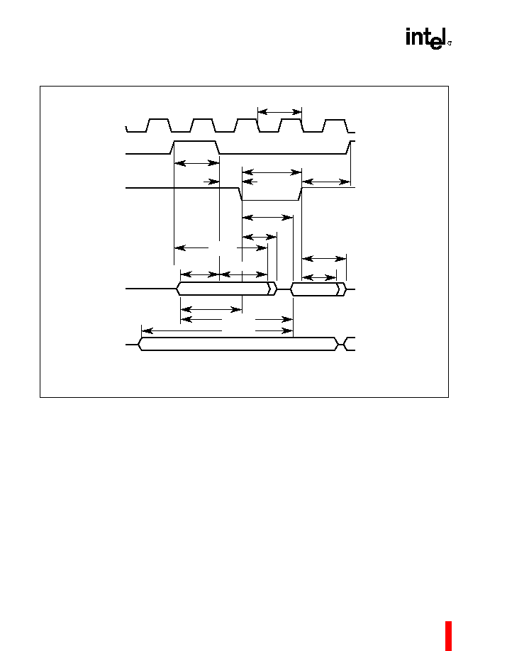
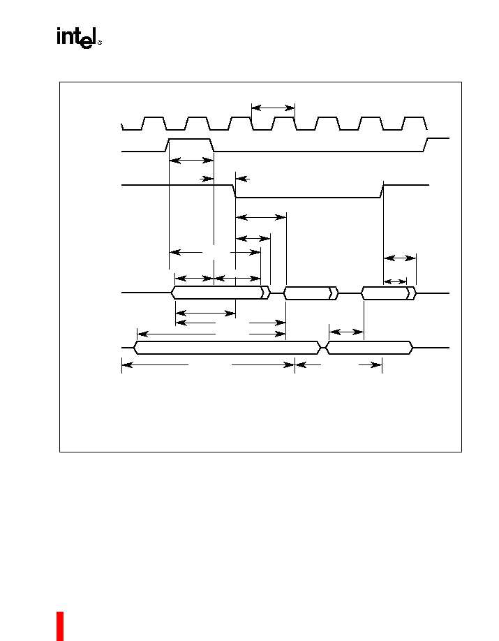
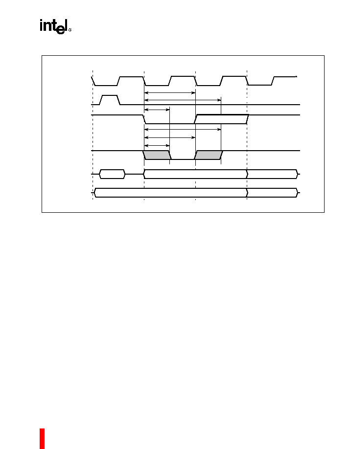
External Bus Cycles, Nonpage Mode
Figure 5. External Bus Cycle: Code Fetch (Nonpage Mode)
XTAL1
ALE
TLHLL
A7:0
TRHDZ1
RD#/PSEN#
P0
P2/A16/A17
TRHDX
TRHLH1
TRLRH
TLLRL
TAVLL
TRLDV
TAVRL
TAVDV1
TAVDV2
TOSC
A4211-03
TLHAX
Instruction In
The value of this parameter depends on wait states. See the table of AC characteristics.
A15:8/A16/A17
D7:0
TRLAZ
TLLAX
8xC251TA/TB/TP/TQ HIGH-PERFORMANCE CHMOS MICROCONTROLLER
ADVANCE INFORMATION
19
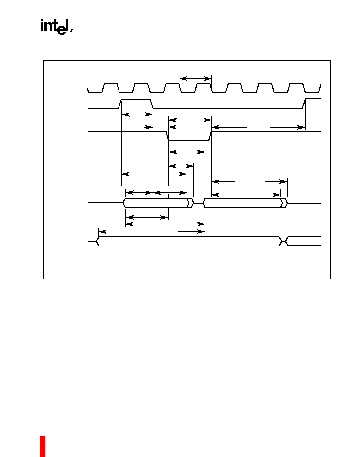
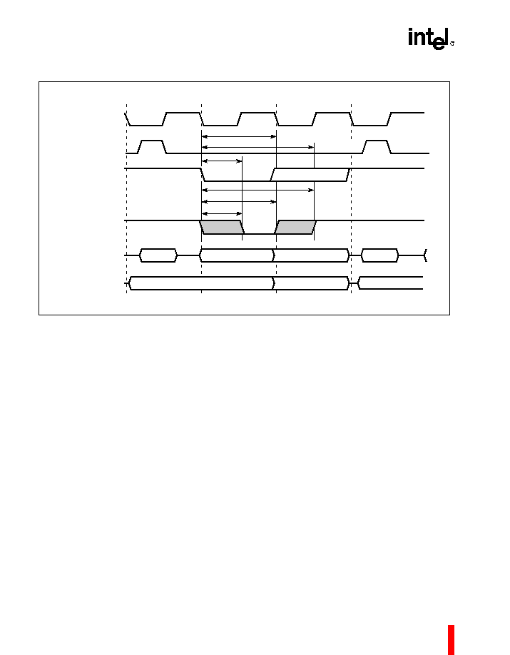
Figure 6. External Bus Cycle: Data Read (Nonpage Mode)
XTAL1
ALE
TLHLL
A7:0
D7:0
RD#/PSEN#
P0
P2/A16/A17
TRHDX
TRHLH2
TRLRH
TLLRL
TAVLL
TLLAX
TRLDV
TAVRL
TAVDV1
TAVDV2
TOSC
A4210-03
TLHAX
Data In
The value of this parameter depends on wait states. See the table of AC characteristics.
A15:8/A16/A17
TRHDZ2
TRLAZ
8xC251TA/TB/TP/TQ HIGH-PERFORMANCE CHMOS MICROCONTROLLER
20
ADVANCE INFORMATION
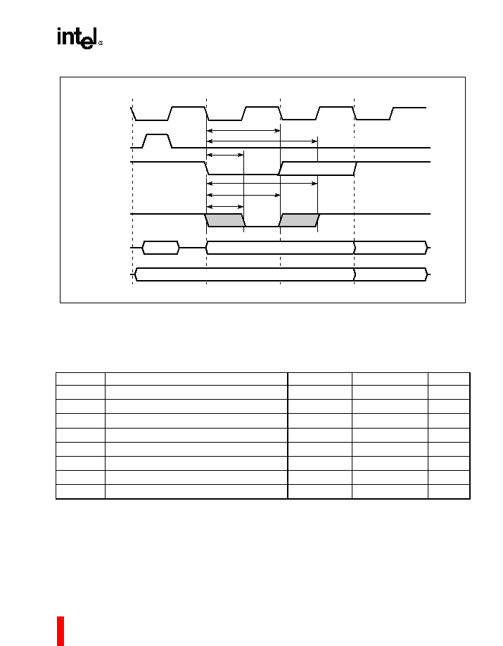
Figure 7. External Bus Cycle: Data Write (Nonpage Mode)
WR#
P0
P2/A16/A17
TLHLL
TWLWH
TWHLH
A4179-01
XTAL1
ALE
TOSC
TWHQX
TQVWH
TWHQX
TAVWL1
TAVWL2
TWHAX
A7:0
D7:0
Data Out
A15:8/A16/A17
The value of this parameter depends on wait states. See the table of AC characteristics.
TLLAX
TLHAX
TAVLL
8xC251TA/TB/TP/TQ HIGH-PERFORMANCE CHMOS MICROCONTROLLER
ADVANCE INFORMATION
21
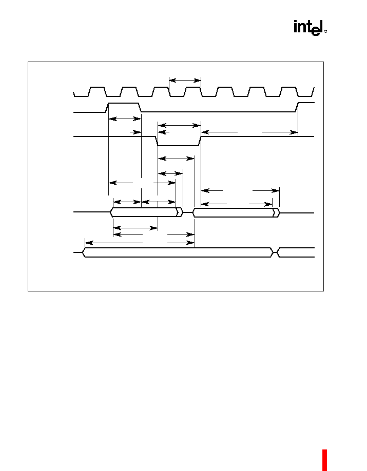
6.3.2
External Bus Cycles, Page Mode
Figure 8. External Bus Cycle: Code Fetch (Page Mode)
XTAL1
ALE
TLHLL
A15:8
D7:0
TRHDZ1
RD#/PSEN#
P2
P0/A16/A17
TRHDX
TLLRL
TAVLL
TRLDV
TRLAZ
TAVRL
TAVDV1
TAVDV2
TOSC
A4213-02
TLHAX
Instruction In
A7:0/A16/A17
D7:0
Instruction In
A7:0/A16/A17
Page Miss
Page Hit
TAVDV3
The value of this parameter depends on wait states. See the table of AC characteristics.
A page hit (i.e., a code fetch to the same 256-byte "page" as the previous code fetch) requires one
state (2T
OSC
); a page miss requires two states (4T
OSC
).
During a sequence of page hits, PSEN# remains low until the end of the last page-hit cycle.
TLLAX
8xC251TA/TB/TP/TQ HIGH-PERFORMANCE CHMOS MICROCONTROLLER
22
ADVANCE INFORMATION
Figure 9. External Bus Cycle: Data Read (Page Mode)
XTAL1
ALE
TLHLL
TRHDZ2
RD#/PSEN#
P2
P0/A16/A17
TRHDX
TRHLH2
TRLRH
TLLRL
TAVLL
TRLDV
TRLAZ
TAVRL
TAVDV1
TAVDV2
TOSC
A4212-03
TLHAX
Data In
The value of this parameter depends on wait states. See the table of AC characteristics.
A15:8
A7:0/A16/A17
D7:0
TLLAX
8xC251TA/TB/TP/TQ HIGH-PERFORMANCE CHMOS MICROCONTROLLER
ADVANCE INFORMATION
23
Figure 10. External Bus Cycle: Data Write (Page Mode)
WR#
P2
P0/A16/A17
TLHLL
TWLWH
TWHLH
A4182-01
XTAL1
ALE
TOSC
TWHQX
TQVWH
TWHQX
TAVWL1
TAVWL2
TWHAX
A15:8
D7:0
Data Out
A7:0/A16/A17
The value of this parameter depends on wait states. See the table of AC characteristics.
TAVLL
TLLAX
TLHAX
8xC251TA/TB/TP/TQ HIGH-PERFORMANCE CHMOS MICROCONTROLLER
24
ADVANCE INFORMATION
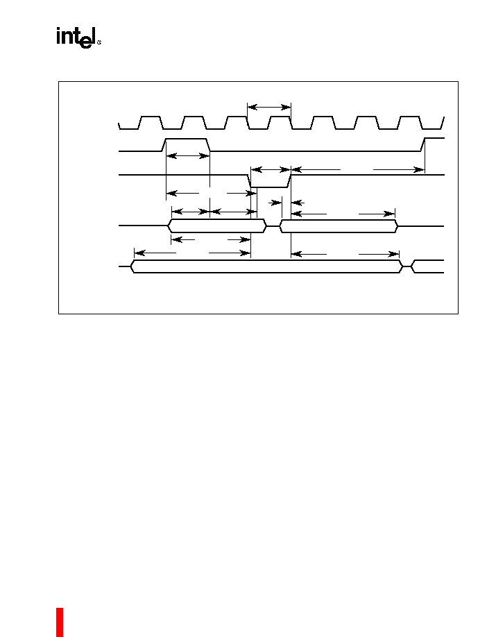
6.3.3
Definition of Real-Time Wait Symbols
6.3.4
External Bus Cycles, Real-Time Wait States
Figure 11. External Bus Cycle: Code Fetch/Data Read (Nonpage Mode)
Table 12. Real-time Wait Timing Symbol Definitions
Signals
Conditions
A
Address
L
Low
D
Data
X
Hold
C
WCLK
V
Setup
Y
WAIT#
W
WR#
R
RD#/PSEN#
A7:0
WCLK
ALE
RD#/PSEN#
WAIT#
P0
P2
A15:8
A5000-02
State 1
State 2
State 3
State 1 (next cycle)
T
CLYX
min
T
CLYV
A7:0
D7:0
stretched
A15:8
stretched
RD#/PSEN# stretched
T
CLYX
max
T
RLYV
T
RLYX
max
T
RLYX
min
8xC251TA/TB/TP/TQ HIGH-PERFORMANCE CHMOS MICROCONTROLLER
ADVANCE INFORMATION
25
Figure 12. External Bus Cycle: Data Write (Nonpage Mode)
A7:0
WCLK
ALE
WR#
T
WLYV
WAIT#
P0
P2
A5002-02
State 1
State 2
State 3
State 4
T
CLYX
min
T
CLYV
D7:0
stretched
A15:8
stretched
WR# stretched
T
WLYX
max
T
WLYX
min
T
CLYX
max
8xC251TA/TB/TP/TQ HIGH-PERFORMANCE CHMOS MICROCONTROLLER
26
ADVANCE INFORMATION
Figure 13. External Bus Cycle: Code Fetch/Data Read (Page Mode)
A15:8
WCLK
ALE
RD#/PSEN#
WAIT#
P2
P0
A7:0
A5001-02
State 1
State 2
State 3
State 1 (next cycle)
T
CLYX
min
T
CLYV
A15:8
D7:0
stretched
A7:0
stretched
RD#/PSEN# stretched
T
CLYX
max
T
RLYV
T
RLYX
max
T
RLYX
min
8xC251TA/TB/TP/TQ HIGH-PERFORMANCE CHMOS MICROCONTROLLER
ADVANCE INFORMATION
27
Figure 14. External Bus Cycle: Data Write (Page Mode)
Table 13. Real-Time Wait AC Timing
Symbol
Parameter
Min
Max
Units
T
CLYV
Wait Clock Low to Wait Set-up
0
T
OSC
≠ 13
ns
T
CLYX
Wait Hold after Wait Clock Low
(2W)T
OSC
+ 5
(1+2W)T
OSC
≠ 20
ns (1)
T
RLYV
PSEN#/RD# Low to Wait Set-up
0
T
OSC
≠ 13
ns
T
RLYVA
PSEN#/RD# Low to Wait Set-up
0
T
OSC
≠ 35
ns (2)
T
RLYX
Wait Hold after PSEN#/RD# Low
(2W)T
OSC
+ 5
(1+2W)T
OSC
≠ 20
ns (1)
T
WLYV
WR# Low to Wait Set-up
0
T
OSC
≠ 13
ns
T
WLYVA
WR# Low to Wait Set-up
0
T
OSC
≠ 35
ns (2)
T
WLYX
Wait Hold after WR# Low
(2W)T
OSC
+ 5
(1+2W)T
OSC
≠ 20
ns (1)
NOTES:
1. W = 0, 1, 2 -- is the number of real time wait states.
2. Device configured with the extended data float timing.
A15:8
WCLK
ALE
WR#
T
WLYV
WAIT#
P2
P0
A5003-02
State 1
State 2
State 3
State 4
T
CLYX
min
T
CLYV
D7:0
stretched
A7:0
stretched
WR# stretched
T
WLYX
max
T
WLYX
min
T
CLYX
max
8xC251TA/TB/TP/TQ HIGH-PERFORMANCE CHMOS MICROCONTROLLER
28
ADVANCE INFORMATION
6.4
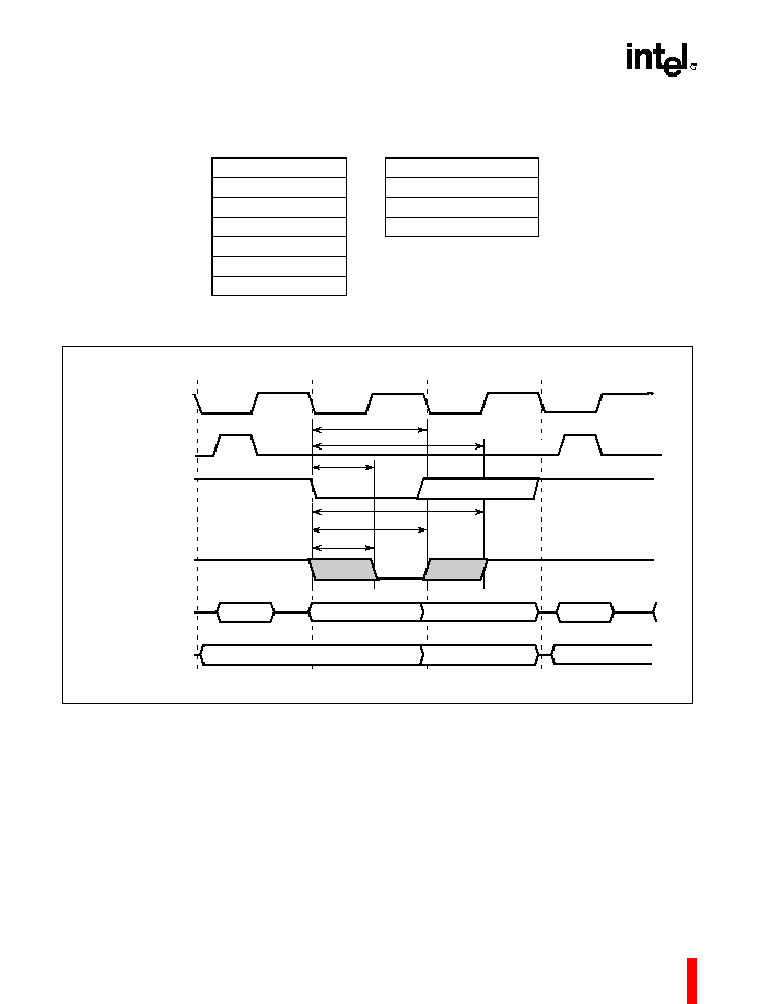
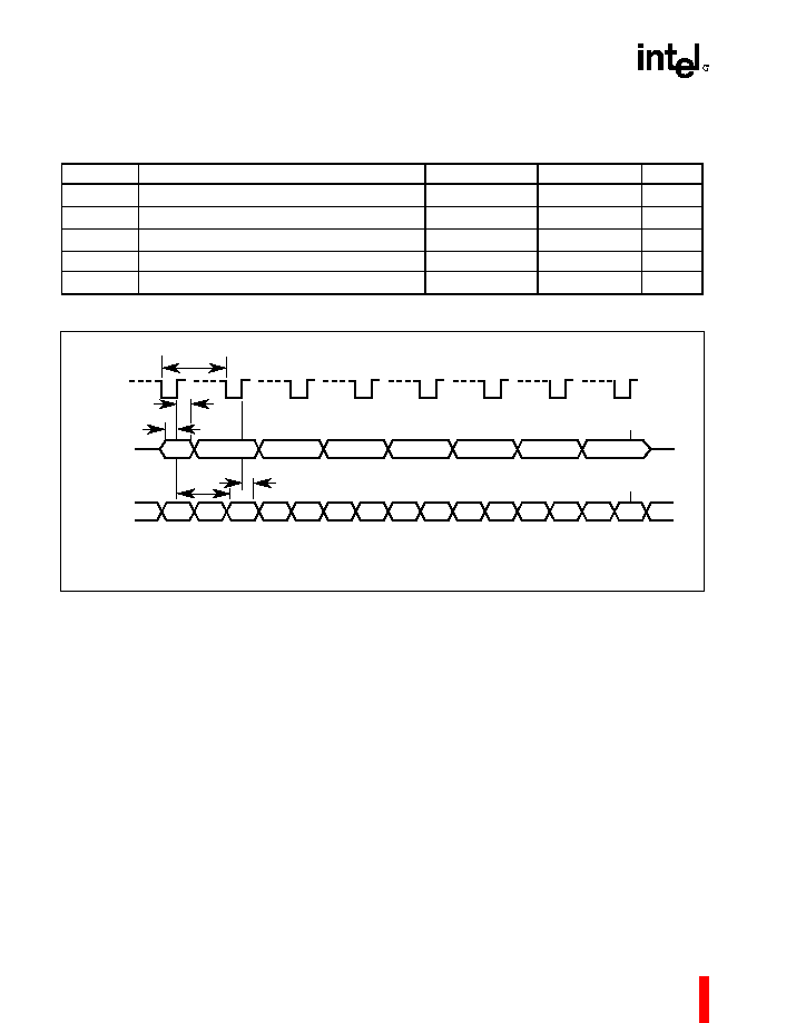
AC Characteristics -- Serial Port, Shift Register Mode
Figure 15. Serial Port Waveform -- Shift Register Mode
Table 14. Serial Port Timing -- Shift Register Mode
Symbol
Parameter
Min
Max
Units
T
XLXL
Serial Port Clock Cycle Time
12T
OSC
ns
T
QVSH
Output Data Setup to Clock Rising Edge
10T
OSC
≠ 133
ns
T
XHQX
Output Data hold after Clock Rising Edge
2T
OSC
≠ 117
ns
T
XHDX
Input Data Hold after Clock Rising Edge
0
ns
T
XHDV
Clock Rising Edge to Input Data Valid
10T
OSC
≠ 133
ns
Valid
Valid
Valid
Valid
Valid
Valid
Valid
Valid
RXD
(In)
RXD
(Out)
TXD
0
1
2
3
4
5
6
7
TQVXH
TXLXL
TXHDX
TXHQX
TXHDV
A2592-02
Set TI
Set RI
TAV
TI and RI are set during S1P1 of the peripheral cycle following the shift of the eighth bit.
8xC251TA/TB/TP/TQ HIGH-PERFORMANCE CHMOS MICROCONTROLLER
ADVANCE INFORMATION
29
6.5
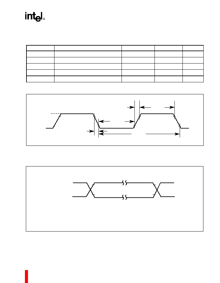
External Clock Drive
Figure 16. External Clock Drive Waveforms
Figure 17. AC Testing Input, Output Waveforms
Table 15. External Clock Drive
Symbol
Parameter
Min
Max
Units
1/T
CLCL
Oscillator Frequency (F
OSC
)
24
MHz
T
CHCX
High Time
20
ns
T
CLCX
Low Time
20
ns
T
CLCH
Rise Time
10
ns
T
CHCL
Fall Time
10
ns
0.7 V
CC
A4119-01
0.45 V
V
CC
≠ 0.5
0.2 V
CC
≠ 0.1
T
CHCL
T
CLCX
T
CLCL
T
CLCH
T
CHCX
AC inputs during testing are driven at V
CC
≠ 0.5V for a logic 1
and 0.45 V for a logic 0. Timing measurements are made at
0.45 V
Inputs
Outputs
A4118-01
V
IH MIN
V
OL MAX
V
CC
≠ 0.5
0.2 V
CC
+ 0.9
0.2 V
CC
≠ 0.1
a min of V
IH
for a logic 1 and V
OL
for a logic 0.
8xC251TA/TB/TP/TQ HIGH-PERFORMANCE CHMOS MICROCONTROLLER
30
ADVANCE INFORMATION
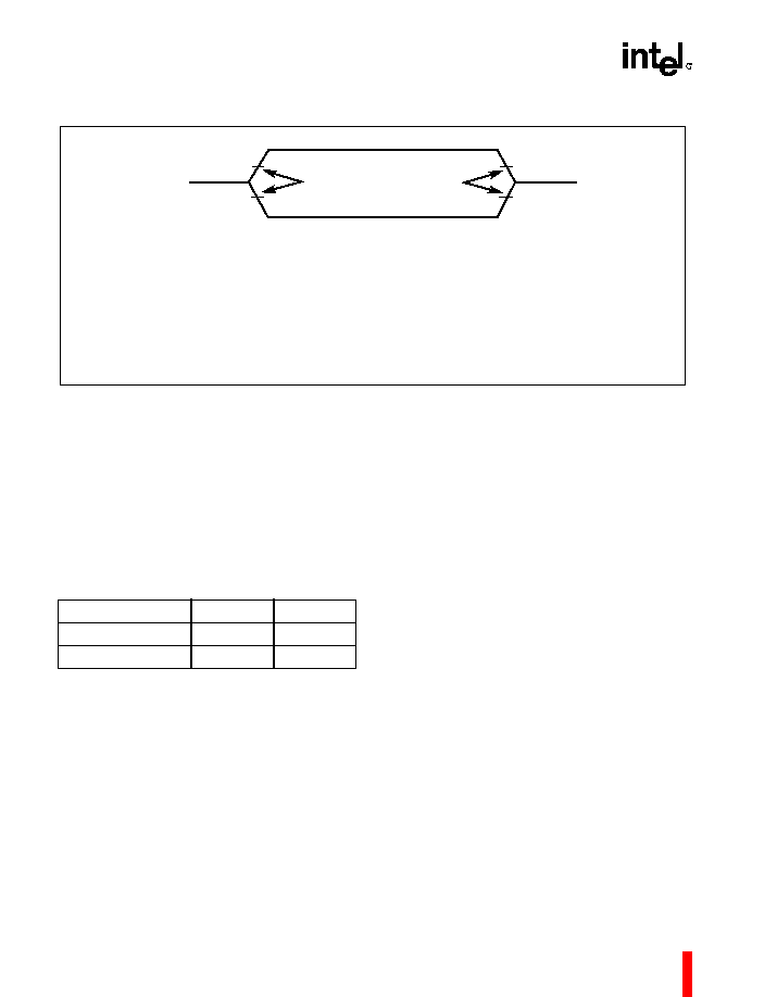
Figure 18. Float Waveforms
V
LOAD
+ 0.1 V
V
LOAD
≠ 0.1 V
Timing Reference
Points
V
LOAD
V
OH
≠ 0.1 V
V
OL
+ 0.1 V
For timing purposes, a port pin is no longer floating when a
100 mV change from load voltage occurs and begins to float
when a 100 mV change from the loading V
OH
/V
OL
level occurs
with I
OL/
I
OH
=
± 20 mA.
A4117-01
7.0
THERMAL CHARACTERISTICS
All thermal impedance data is approximate for static
air conditions at 1 watt of power dissipation. Values
change depending on operating conditions and
application requirements. The Intel
Packaging
Handbook
(order number 240800) describes Intel's
thermal impedance test methodology.
Table 16. Thermal Characteristics
Package Type
JA
JC
44-pin PLCC
46∞C/W
16∞C/W
40-pin PDIP
45∞C/W
16∞C/W