 | –≠–ª–µ–∫—Ç—Ä–æ–Ω–Ω—ã–π –∫–æ–º–ø–æ–Ω–µ–Ω—Ç: 8XL196NP | –°–∫–∞—á–∞—Ç—å:  PDF PDF  ZIP ZIP |

Information in this document is provided solely to enable use of Intel products. Intel assumes no liability whatsoever, including infringe-
ment of any patent or copyright, for sale and use of Intel products except as provided in Intel's Terms and Conditions of Sale for such
products. Information contained herein supersedes previously published specifications on these devices from Intel.
© INTEL CORPORATION, 1996
March 1996
8XL196NP COMMERCIAL
CHMOS 16-BIT MICROCONTROLLER
The 8XL196NP is a member of Intel's 16-bit MCS
Æ
96 microcontroller family. The device features 1 Mbyte of
linear address space, a demultiplexed bus, and a chip-select unit. The external bus can dynamically switch
between multiplexed and demultiplexed operation. When operating at 14 MHz in demultiplexed mode, the
8XL196NP can access a 200 ns memory device with zero wait states. The 8XL196NP is available without
ROM (80L196NP) or with 4 Kbytes of ROM (83L196NP).
n
14 MHz Operation at 2.7≠3.3 Volts
n
1 Mbyte of Linear Address Space
n
Optional 4 Kbytes of ROM
n
1000 Bytes of Register RAM
n
Register-register Architecture
n
32 I/O Port Pins
n
16 Prioritized Interrupt Sources
n
4 External Interrupt Pins and NMI Pin
n
2 Flexible 16-bit Timer/Counters with
Quadrature Counting Capability
n
3 Pulse-width Modulator (PWM) Outputs
with High Drive Capability
n
Full-duplex Serial Port with Dedicated
Baud-rate Generator
n
Peripheral Transaction Server
n
Event Processor Array (EPA) with 4 High-
speed Capture/Compare Channels
n
Chip-select Unit
-- 6 Chip Select Pins
-- Dynamic Demultiplexed/Multi-
plexed Address/Data Bus for Each
Chip Select
-- Programmable Wait States (0, 1, 2,
or 3) for Each Chip Select
-- Programmable Bus Width (8- or 16-
bit) for Each Chip Select
-- Programmable Address Range for
Each Chip Select
n
2.0
µ
s 16
◊
16 Unsigned Multiplication
n
3.4
µ
s 32/16 Unsigned Division
n
100-pin SQFP or 100-pin QFP Package
n
Complete System Development
Support
n
High-speed CHMOS Technology
Order Number: 272824-001
8XL196NP COMMERCIAL CHMOS 16-BIT MICROCONTROLLER
2
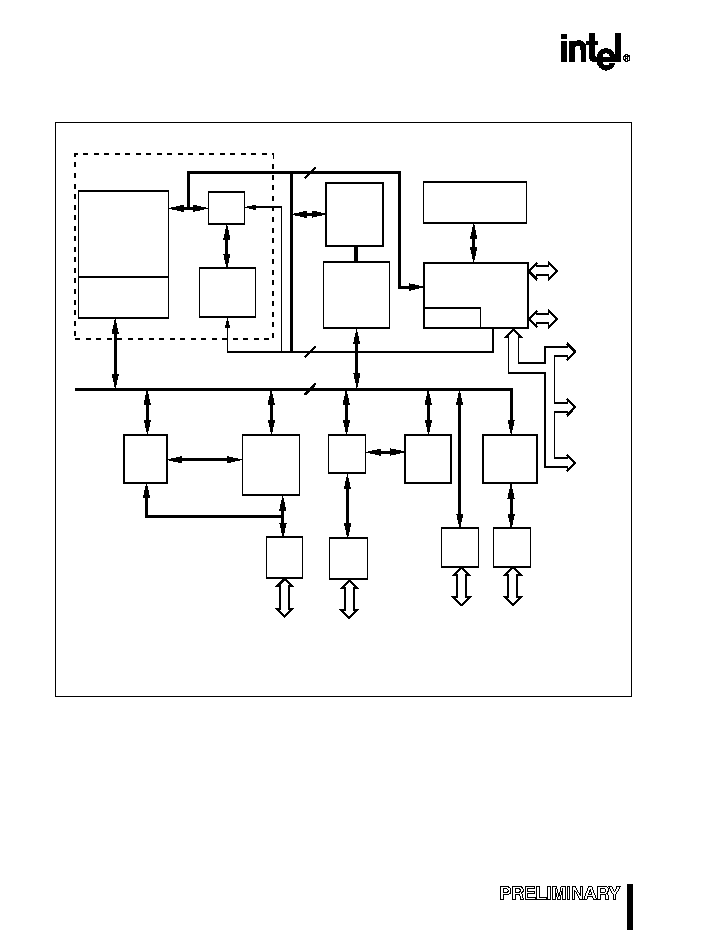
Figure 1. 8XL196NP Block Diagram
Timer 1
Timer 2
Event
Processor
Array
Serial
Port
Baud
Rate
Gen
Port 2
Port 1
Port 1/
EPA3:0,
Timer 1,
Timer 2
Port 2/
Hold Control,
SIO,
EXTINT1:0
Pulse
Width
Modulator
Microcode
Engine
RALU
CPU
Peripheral
Transaction
Server
4K Bytes
ROM (optional)
AD15:0
A15:0
A19:16/
EPORT3:0
Chip Select
CS5:0#
Interrupt
Controller
16
16
8
1000
Byte
Register
File
24 Bytes
CPU SFRs
Memory Controller
with
Chip Select
Queue
Port
3
Port
4
Port 3/
EXTINT3:2
Port 4/
PWM2:0
A2351-01
Control
Signals
8XL196NP COMMERCIAL CHMOS 16-BIT MICROCONTROLLER
3
1.0 NOMENCLATURE OVERVIEW
Figure 2. 8XL196NP Family Nomenclature
Table 1. Description of Product Nomenclature
Parameter
Options
Description
Temperature and Burn-in Options
no mark
Commercial operating temperature range (0∞C to 70∞C)
with Intel standard burn-in.
Packaging Options
S
SB
QFP
SQFP
Program≠memory Options
0
3
No ROM
ROM
Process Information
L
Low Voltage CHMOS
Product Family
196NP
Device Speed
no mark
14 MHz
Program-memory Options
XXXXX
XX
X
X
8
XX
X
Packaging Options
Temperature and Burn-in Options
A2815-01
Process Information
Product Family Device Speed
8XL196NP COMMERCIAL CHMOS 16-BIT MICROCONTROLLER
4
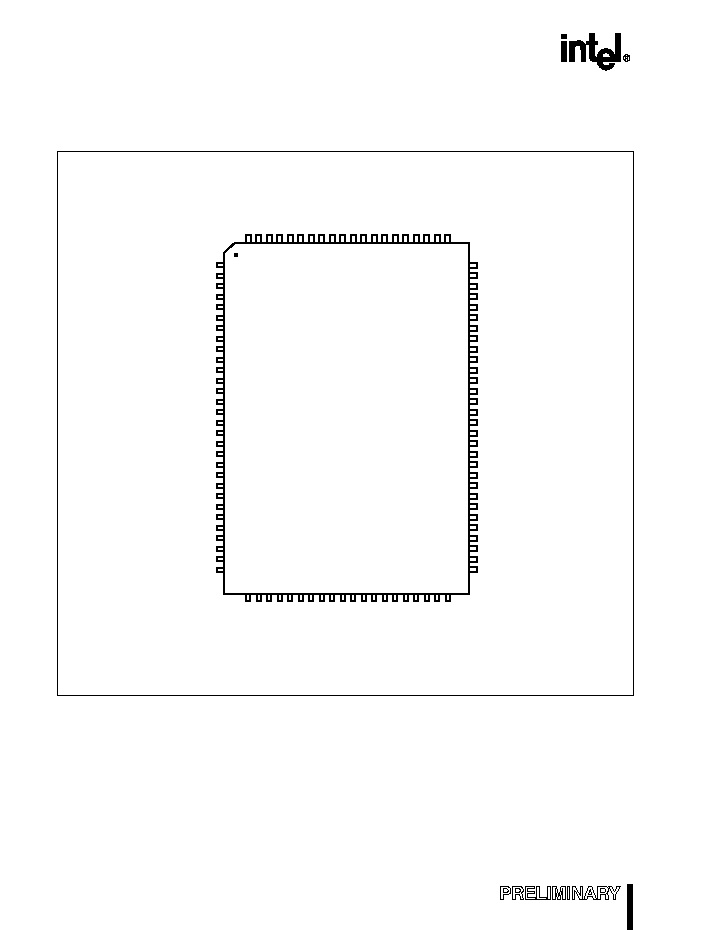
2.0 PINOUT
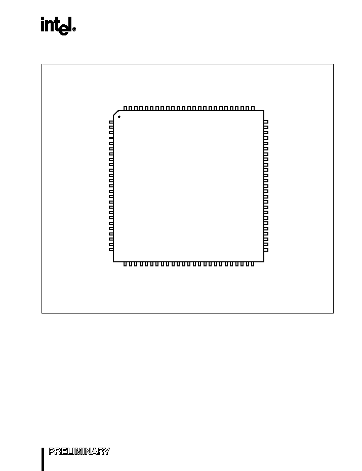
Figure 3. 8XL196NP 100-pin SQFP Package
V
SS
A18 / EPORT.2
A19 / EPORT.3
WR# / WRL#
RD#
BHE# / WRH#
ALE
INST
READY
RPD
ONCE
V
SS
V
CC
V
SS
A8
A9
A10
A11
A12
A13
A14
A15
V
SS
XTAL1
XTAL2
V
SS
P2.7 / CLKOUT
NC
P2.6 / HLDA#
P2.5 / HOLD#
AD1
AD2
AD3
AD4
AD5
AD6
AD7
V
CC
AD8
V
SS
AD9
AD10
AD11
AD12
AD13
AD14
AD15
A16 / EPORT.0
A17 / EPORT.1
V
CC
A4318-01
AD0
NC
RESET#
NMI
EA#
A0
A1
V
CC
V
SS
A2
A3
A4
A5
A6
A7
V
CC
V
SS
NC
P3.0 / CS0#
P3.1 / CS1#
P3.2 / CS2#
P3.3 / CS3#
V
SS
P3.4 / CS4#
P3.5 / CS5#
P3.6 / EXTINT2
NC
P3.7 / EXTINT3
P1.0 / EPA0
V
CC
80
79
78
77
76
75
74
73
72
71
70
69
68
67
66
65
64
63
62
61
60
59
58
57
56
55
54
53
52
51
S8XL196NP
View of component as
mounted on PC board
1
2
3
4
5
6
7
8
9
10
11
12
13
14
15
16
17
18
19
20
21
22
23
24
25
26
27
28
29
30
P1.1 / EPA1
P1.2 / EPA2
P1.3 / EPA3
P1.4 / T1CLK
P1.5 / T1DIR
V
CC
P1.6 / T2CLK
V
SS
P1.7 / T2DIR
P4.0 / PWM0
P4.1 / PWM1
P4.2 / PWM2
P4.3
V
CC
V
SS
P2.0 / TXD
P2.1 / RXD
P2.2 / EXTINT0
P2.3 / BREQ#
P2.4 / EXTINT1
31
32
33
34
35
36
37
38
39
40
41
42
43
44
45
46
47
48
49
50
100
99
98
97
96
95
94
93
92
91
90
89
88
87
86
85
84
83
82
81

8XL196NP COMMERCIAL CHMOS 16-BIT MICROCONTROLLER
5
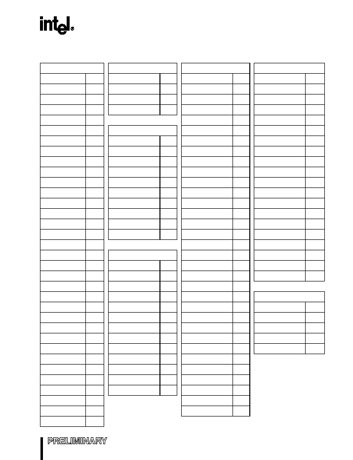
Table 2. 8XL196NP 100-pin SQFP Pin Assignment
Pin
Name
Pin
Name
Pin
Name
Pin
Name
1
RESET#
26
EXTINT3/P3.7
51
CLKOUT/P2.7
76
WR#/WRL#
2
NMI
27
EPA0/P1.0
52
NC
77
EPORT.3/A19
3
EA#
28
V
CC
53
V
SS
78
EPORT.2/A18
4
A0
29
EPA1/P1.1
54
XTAL2
79
V
SS
5
A1
30
EPA2/P1.2
55
XTAL1
80
V
CC
6
V
CC
31
EPA3/P1.3
56
V
SS
81
EPORT.1/A17
7
V
SS
32
T1CLK/P1.4
57
NC
82
EPORT.0/A16
8
A2
33
T1DIR/P1.5
58
A15
83
AD15
9
A3
34
V
CC
59
A14
84
AD14
10
A4
35
T2CLK/P1.6
60
A13
85
AD13
11
A5
36
V
SS
61
A12
86
AD12
12
A6
37
T2DIR/P1.7
62
A11
87
AD11
13
A7
38
PWM0/P4.0
63
A10
88
AD10
14
V
CC
39
PWM1/P4.1
64
A9
89
AD9
15
V
SS
40
PWM2/P4.2
65
A8
90
V
SS
16
NC
41
P4.3
66
V
SS
91
AD8
17
NC
42
V
CC
67
V
CC
92
V
CC
18
CS0#/P3.0
43
V
SS
68
V
SS
93
AD7
19
CS1#/P3.1
44
TXD/P2.0
69
ONCE
94
AD6
20
CS2#/P3.2
45
RXD/P2.1
70
RPD
95
AD5
21
CS3#/P3.3
46
EXTINT0/P2.2
71
READY
96
AD4
22
V
SS
47
BREQ#/P2.3
72
INST
97
AD3
23
CS4#/P3.4
48
EXTINT1/P2.4
73
ALE
98
AD2
24
CS5#/P3.5
49
HOLD#/P2.5
74
BHE#/WRH#
99
AD1
25
EXTINT2/P3.6
50
HLDA#/P2.6
75
RD#
100
AD0
To be compatible with future versions of the N
x
family, tie the no connection (NC) pins as follows:
Pin 57 = V
SS
, Pin 16 = V
CC
, Pin 17 = V
SS
(5 volts on this pin will enable a clock doubler on future
devices), and Pin 52 = V
CC
.
8XL196NP COMMERCIAL CHMOS 16-BIT MICROCONTROLLER
6
Table 3. 100-pin SQFP Pin Assignment Arranged by Functional Categories
Address & Data
Address & Data (cont)
Input/Output
Power & Ground
Name
Pin
Name
Pin
Name
Pin
Name
Pin
A0
4
AD13
85
CS0#/P3.0
18
V
CC
6
A1
5
AD14
84
CS1#/P3.1
19
V
CC
14
A2
8
AD15
83
CS2#/P3.2
20
V
CC
28
A3
9
CS3#/P3.3
21
V
CC
34
A4
10
Bus Control & Status
CS4#/P3.4
23
V
CC
42
A5
11
Name
Pin
CS5#/P3.5
24
V
CC
67
A6
12
ALE
73
EPA0/P1.0
27
V
CC
80
A7
13
BHE#/WRH#
74
EPA1/P1.1
29
V
CC
92
A8
65
BREQ#
47
EPA2/P1.2
30
V
SS
7
A9
64
HOLD#
49
EPA3/P1.3
31
V
SS
15
A10
63
HLDA#
50
EPORT.0
82
V
SS
22
A11
62
INST
72
EPORT.1
81
V
SS
36
A12
61
RD#
75
EPORT.2
78
V
SS
43
A13
60
READY
71
EPORT.3
77
V
SS
53
A14
59
WR#/WRL#
76
P2.2
46
V
SS
56
A15
58
P2.3
47
V
SS
66
A16
82
Processor Control
P2.4
48
V
SS
68
A17
81
Name
Pin
P2.5
49
V
SS
79
A18
78
CLKOUT
51
P2.6
50
V
SS
90
A19
77
EA#
3
P2.7
51
AD0
100
EXTINT0
46
P3.6
25
No Connection
AD1
99
EXTINT1
48
P3.7
26
Name
Pin
AD2
98
EXTINT2
25
P4.3
41
NC
16
AD3
97
EXTINT3
26
PWM0/P4.0
38
NC
17
AD4
96
NMI
2
PWM1/P4.1
39
NC
52
AD5
95
ONCE
69
PWM2/P4.2
40
NC
57
AD6
94
RESET#
1
RXD/P2.1
45
AD7
93
RPD
70
T1CLK/P1.4
32
AD8
91
XTAL1
55
T1DIR/P1.5
33
AD9
89
XTAL2
54
T2CLK/P1.6
35
AD10
88
T2DIR/P1.7
37
AD11
87
TXD/P2.0
44
AD12
86
8XL196NP COMMERCIAL CHMOS 16-BIT MICROCONTROLLER
7
Figure 4. 8XL196NP 100-pin QFP Package
RD#
BHE# / WRH#
ALE
INST
READY
RPD
ONCE
V
SS
V
CC
V
SS
A8
A9
A10
A11
A12
A13
A14
A15
NC
V
SS
XTAL1
XTAL2
V
SS
NC
P2.7 / CLKOUT
AD0
AD1
AD2
AD3
AD4
AD5
AD6
AD7
V
CC
AD8
V
SS
AD9
AD10
AD11
AD12
AD13
AD14
AD15
A16 / EPORT.0
A17 / EPORT.1
V
CC
V
SS
A18 / EPORT.2
A19 / EPORT.3
WR# / WRL#
A4317-01
RESET#
NMI
EA#
A0
A1
V
CC
V
SS
A2
A3
A4
A5
A6
A7
V
CC
V
SS
NC
NC
P3.0 / CS0#
P3.1 / CS1#
P3.2 / CS2#
P3.3 / CS3#
V
SS
P3.4 / CS4#
P3.5 / CS5#
P3.6 / EXTINT2
75
74
73
72
71
70
69
68
67
66
65
64
63
62
61
60
59
58
57
56
55
54
53
52
51
SB8XL196NP
View of component as
mounted on PC board
1
2
3
4
5
6
7
8
9
10
11
12
13
14
15
16
17
18
19
20
21
22
23
24
25
P3.7 / EXTINT3
P1.0 / EPA0
V
CC
P1.1 / EPA1
P1.2 / EPA2
P1.3 / EPA3
P1.4 / T1CLK
P1.5 / T1DIR
V
CC
P1.6 / T2CLK
V
SS
P1.7 / T2DIR
P4.0 / PWM0
P4.1 / PWM1
P4.2 / PWM2
P4.3
V
CC
V
SS
P2.0 / TXD
P2.1 / RXD
P2.2 / EXTINT0
P2.3 / BREQ#
P2.4 / EXTINT1
P2.5 / HOLD#
P2.6 / HLDA#
26
27
28
29
30
31
32
33
34
35
36
37
38
39
40
41
42
43
44
45
46
47
48
49
50
100
99
98
97
96
95
94
93
92
91
90
89
88
87
86
85
84
83
82
81
80
79
78
77
76

8XL196NP COMMERCIAL CHMOS 16-BIT MICROCONTROLLER
8
Table 4. 8XL196NP 100-pin QFP Pin Assignment
Pin
Name
Pin
Name
Pin
Name
Pin
Name
1
AD0
26
EXTINT2/P3.6
51
HOLD#/P2.5
76
RD#
2
No Connection
27
No Connection
52
HLDA#/P2.6
77
WR#/WRL#
3
RESET#
28
EXTINT3/P3.7
53
No Connection
78
EPORT.3/A19
4
NMI
29
EPA0/P1.0
54
CLKOUT/P2.7
79
EPORT.2/A18
5
EA#
30
V
CC
55
V
SS
80
V
SS
6
A0
31
EPA1/P1.1
56
XTAL2
81
V
CC
7
A1
32
EPA2/P1.2
57
XTAL1
82
EPORT.1/A17
8
V
CC
33
EPA3/P1.3
58
V
SS
83
EPORT.0/A16
9
V
SS
34
T1CLK/P1.4
59
A15
84
AD15
10
A2
35
T1DIR/P1.5
60
A14
85
AD14
11
A3
36
V
CC
61
A13
86
AD13
12
A4
37
T2CLK/P1.6
62
A12
87
AD12
13
A5
38
V
SS
63
A11
88
AD11
14
A6
39
T2DIR/P1.7
64
A10
89
AD10
15
A7
40
PWM0/P4.0
65
A9
90
AD9
16
V
CC
41
PWM1/P4.1
66
A8
91
V
SS
17
V
SS
42
PWM2/P4.2
67
V
SS
92
AD8
18
No Connection
43
P4.3
68
V
CC
93
V
CC
19
CS0#/P3.0
44
V
CC
69
V
SS
94
AD7
20
CS1#/P3.1
45
V
SS
70
ONCE
95
AD6
21
CS2#/P3.2
46
TXD/P2.0
71
RPD
96
AD5
22
CS3#/P3.3
47
RXD/P2.1
72
READY
97
AD4
23
V
SS
48
EXTINT0/P2.2
73
INST
98
AD3
24
CS4#/P3.4
49
BREQ#/P2.3
74
ALE
99
AD2
25
CS5#/P3.5
50
EXTINT1/P2.4
75
BHE#/WRH#
100
AD1
8XL196NP COMMERCIAL CHMOS 16-BIT MICROCONTROLLER
9
Table 5. 100-pin QFP Pin Assignment Arranged by Functional Categories
Address & Data
Address & Data (cont)
Input/Output
Power & Ground
Name
Pin
Name
Pin
Name
Pin
Name
Pin
A0
6
AD13
86
CS0#/P3.0
19
V
CC
8
A1
7
AD14
85
CS1#/P3.1
20
V
CC
16
A2
10
AD15
84
CS2#/P3.2
21
V
CC
30
A3
11
CS3#/P3.3
22
V
CC
36
A4
12
Bus Control & Status
CS4#/P3.4
24
V
CC
44
A5
13
Name
Pin
CS5#/P3.5
25
V
CC
68
A6
14
ALE
74
EPA0/P1.0
29
V
CC
81
A7
15
BHE#/WRH#
75
EPA1/P1.1
31
V
CC
93
A8
66
BREQ#
49
EPA2/P1.2
32
V
SS
9
A9
65
HOLD#
51
EPA3/P1.3
33
V
SS
17
A10
64
HLDA#
52
EPORT.0
83
V
SS
23
A11
63
INST
73
EPORT.1
82
V
SS
38
A12
62
RD#
76
EPORT.2
79
V
SS
45
A13
61
READY
72
EPORT.3
78
V
SS
55
A14
60
WR#/WRL#
77
P2.2
48
V
SS
58
A15
59
P2.3
49
V
SS
67
A16
83
Processor Control
P2.4
50
V
SS
69
A17
82
Name
Pin
P2.5
51
V
SS
80
A18
79
CLKOUT
54
P2.6
52
V
SS
91
A19
78
EA#
5
P2.7
54
AD0
1
EXTINT0
48
P3.6
26
No Connection
AD1
100
EXTINT1
50
P3.7
28
Name
Pin
AD2
99
EXTINT2
26
P4.3
43
NC
2
AD3
98
EXTINT3
28
PWM0/P4.0
40
NC
18
AD4
97
NMI
4
PWM1/P4.1
41
NC
27
AD5
96
ONCE
70
PWM2/P4.2
42
NC
53
AD6
95
RESET#
3
RXD/P2.1
47
AD7
94
RPD
71
T1CLK/P1.4
34
AD8
92
XTAL1
57
T1DIR/P1.5
35
AD9
90
XTAL2
56
T2CLK/P1.6
37
AD10
89
T2DIR/P1.7
39
AD11
88
TXD/P2.0
46
AD12
87
8XL196NP COMMERCIAL CHMOS 16-BIT MICROCONTROLLER
10
3.0 SIGNALS
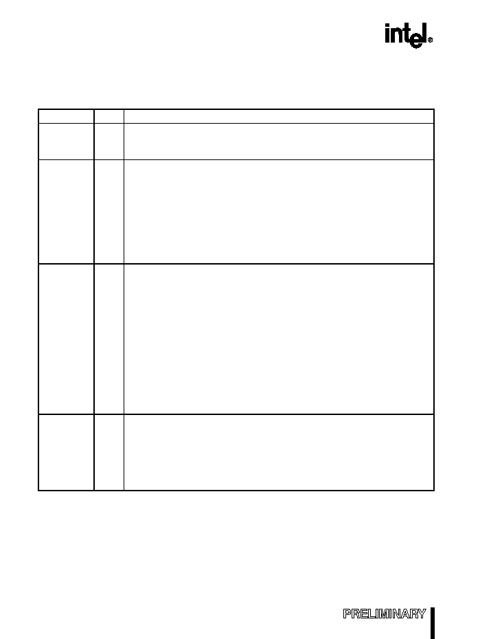
Table 6. Signal Descriptions
Name
Type
Description
A15:0
I/O
System Address Bus
These address pins provide address bits 0≠15 during the entire external memory
cycle during both multiplexed and demultiplexed bus modes.
A19:16
I/O
Address Pins 16≠19
These address pins provide address bits 16≠19 during the entire external memory
cycle during both multiplexed and demultiplexed bus modes, supporting extended
addressing of the 1-Mbyte address space.
NOTE:
Internally, there are 24 address bits; however, only 20 external address
pins (A19:0) are implemented. The internal address space is 16 Mbytes
(000000≠FFFFFFH) and the external address space is 1 Mbyte (00000≠
FFFFFH). The microcontroller resets to FF2080H in internal memory or
F2080H in external memory.
A19:16 share package pins with EPORT.3:0.
AD15:0
I/O
Address/Data Lines
The function of these pins depends on the bus width and mode.
16-bit Multiplexed Bus Mode:
AD15:0 drive address bits 0≠15 during the first half of the bus cycle and drive or
receive data during the second half of the bus cycle.
8-bit Multiplexed Bus Mode:
AD15:8 drive address bits 8≠15 during the entire bus cycle. AD7:0 drive address
bits 0≠7 during the first half of the bus cycle and drive or receive data during the
second half of the bus cycle.
16-bit Demultiplexed Mode:
AD15:0 drive or receive data during the entire bus cycle.
8-bit Demultiplexed Mode:
AD7:0 drive or receive data during the entire bus cycle. AD15:8 drive the data that
is currently on the high byte of the internal bus.
ALE
O
Address Latch Enable
This active-high output signal is asserted only during external memory cycles. ALE
signals the start of an external bus cycle and indicates that valid address
information is available on the system address/data bus (A19:16 and AD15:0 for a
multiplexed bus; A19:0 for a demultiplexed bus).
An external latch can use this signal to demultiplex address bits 0≠15 from the
address/data bus in multiplexed mode.
8XL196NP COMMERCIAL CHMOS 16-BIT MICROCONTROLLER
11
BHE#
O
Byte High Enable
During 16-bit bus cycles, this active-low output signal is asserted for word and high-
byte reads and writes to external memory. BHE# indicates that valid data is being
transferred over the upper half of the system data bus. Use BHE#, in conjunction
with address bit 0 (A0 for a demultiplexed address bus, AD0 for a multiplexed
address/data bus), to determine which memory byte is being transferred over the
system bus:
BHE#
AD0 or A0 Byte(s) Accessed
0
0
both bytes
0
1
high byte only
1
0
low byte only
BHE# shares a package pin with WRH#.
When this pin is configured as a special-function signal (P5_MODE.5 = 1), the
chip configuration register 0 (CCR0) determines whether it functions as BHE# or
WRH#. CCR0.2 = 1 selects BHE#; CCR0.2 = 0 selects WRH#.
BREQ#
O
Bus Request
This active-low output signal is asserted during a hold cycle when the bus controller
has a pending external memory cycle. When the bus-hold protocol is enabled
(WSR.7 is set), the P2.3/BREQ# pin can function only as BREQ#, regardless of the
configuration selected through the port configuration registers (P2_MODE,
P2_DIR, and P2_REG). An attempt to change the pin configuration is ignored until
the bus-hold protocol is disabled (WSR.7 is cleared).
The microcontroller can assert BREQ# at the same time as or after it asserts
HLDA#. Once it is asserted, BREQ# remains asserted until HOLD# is deasserted.
BREQ# shares a package pin with P2.4.
CLKOUT
O
Clock Output
Output of the internal clock generator. The CLKOUT frequency is Ω the internal
operating frequency (f). CLKOUT has a 50% duty cycle.
CLKOUT shares a package pin with P2.7.
CS5#:0
O
Chip-select Lines 0≠5
The active-low output CS
x
# is asserted during an external memory cycle when the
address to be accessed is in the range programmed for chip select
x
. If the external
memory address is outside the range assigned to the six chip selects, no chip-
select output is asserted and the bus configuration defaults to the CS5# values.
Immediately following reset, CS0# is automatically assigned to the range FF2000≠
FF20FFH (F2000≠F20FFH if external).
CS5:0# share package pins with P3.5:0.
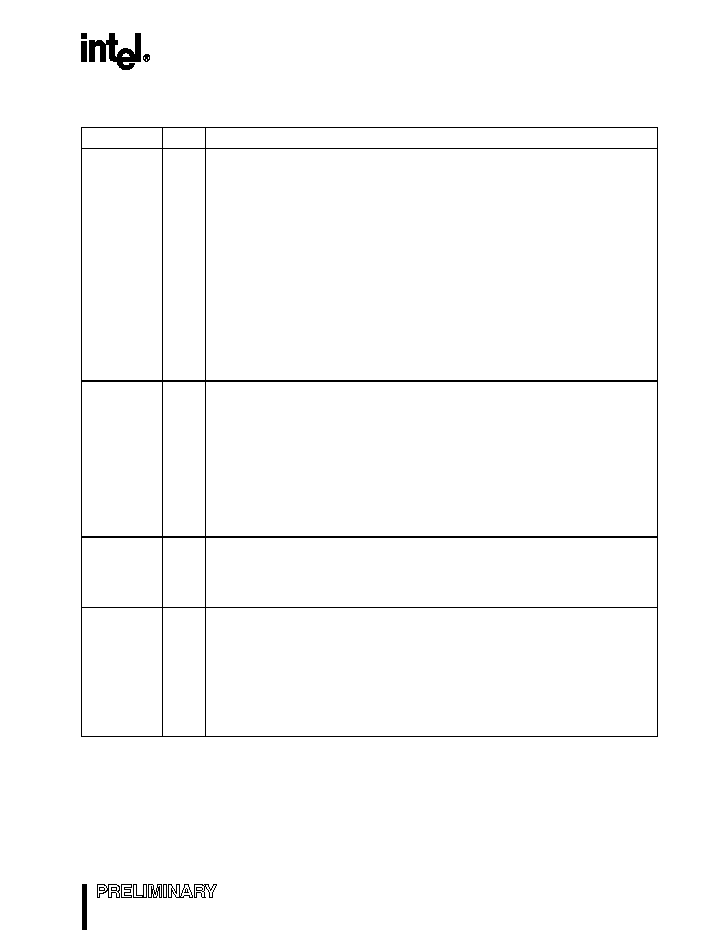
Table 6. Signal Descriptions (Continued)
Name
Type
Description

8XL196NP COMMERCIAL CHMOS 16-BIT MICROCONTROLLER
12
EA#
I
External Access
This input determines whether memory accesses to special-purpose and program
memory partitions (FF2000≠FF2FFFH) are directed to internal or external memory.
These accesses are directed to internal memory if EA# is held high and to external
memory if EA# is held low. For an access to any other memory location, the value
of EA# is irrelevant.
EA# is not latched and can be switched dynamically during normal operating mode.
Be sure to thoroughly consider the issues, such as different access times for
internal and external memory, before using this dynamic switching capability.
Always connect EA# to V
SS
when using a microcontroller that has no internal
nonvolatile memory.
EPA3:0
I/O
Event Processor Array (EPA) Capture/Compare Channels
High-speed input/output signals for the EPA capture/compare channels.
EPA3:0 share package pins with P1.3:0.
EPORT.3:0
I/O
Extended Addressing Port
This is a 4-bit, bidirectional, memory-mapped port.
EPORT.3:0 share package pins with A.19:16.
EXTINT0
EXTINT1
EXTINT2
EXTINT3
I
External Interrupts
In normal operating mode, a rising edge on EXTINT
x
sets the EXTINT
x
interrupt
pending bit. EXTINT
x
is sampled during phase 2 (CLKOUT high). The minimum
high time is one state time.
In standby and powerdown modes, asserting the EXTINT
x
signal for at least 50 ns
causes the device to resume normal operation. The interrupt does not need to be
enabled, but the pin must be configured as a special-function input. If the EXTINT
x
interrupt is enabled, the CPU executes the interrupt service routine. Otherwise, the
CPU executes the instruction that immediately follows the command that invoked
the power-saving mode.
In idle mode, asserting any enabled interrupt causes the device to resume normal
operation.
EXTINT0 shares a package pin with P2.2, EXTINT1 shares a package pin with
P2.4, EXTINT2 shares a package pin with P3.6, and EXTINT3 shares a package
pin with P3.7.
HLDA#
O
Bus Hold Acknowledge
This active-low output indicates that the CPU has released the bus as the result of
an external device asserting HOLD#. When the bus-hold protocol is enabled
(WSR.7 is set), the P2.6/HLDA# pin can function only as HLDA#, regardless of the
configuration selected through the port configuration registers (P2_MODE,
P2_DIR, and P2_REG). An attempt to change the pin configuration is ignored until
the bus-hold protocol is disabled (WSR.7 is cleared).
Table 6. Signal Descriptions (Continued)
Name
Type
Description
8XL196NP COMMERCIAL CHMOS 16-BIT MICROCONTROLLER
13
HOLD#
I
Bus Hold Request
An external device uses this active-low input signal to request control of the bus.
When the bus-hold protocol is enabled (WSR.7 is set), the P2.5/HOLD# pin can
function only as HOLD#, regardless of the configuration selected through the port
configuration registers (P2_MODE, P2_DIR, and P2_REG). An attempt to change
the pin configuration is ignored until the bus-hold protocol is disabled (WSR.7 is
cleared).
HOLD# shares a package pin with P2.5.
INST
O
Instruction Fetch
When high, INST indicates that an instruction is being fetched from external
memory. The signal remains high during the entire bus cycle of an external
instruction fetch. INST is low for data accesses, including interrupt vector fetches
and chip configuration byte reads. INST is low during internal memory fetches.
NMI
I
Nonmaskable Interrupt
In normal operating mode, a rising edge on NMI generates a nonmaskable
interrupt. NMI has the highest priority of all prioritized interrupts. Assert NMI for
greater than one state time to guarantee that it is recognized.
ONCE
I
On-circuit Emulation
Holding ONCE high during the rising edge of RESET# places the device into on-
circuit emulation (ONCE) mode. This mode puts all pins into a high-impedance
state, thereby isolating the device from other components in the system. The value
of ONCE is latched when the RESET# pin goes inactive. While the device is in
ONCE mode, you can debug the system using a clip-on emulator.
To exit ONCE mode, reset the device by pulling the RESET# signal low. To prevent
inadvertent entry into ONCE mode, connect the ONCE pin to V
SS
.
P1.7:0
I/O
Port 1
This is a standard, 8-bit, bidirectional port that shares package pins with individually
selectable special-function signals.
Port 1 shares package pins with the following signals: P1.0/EPA0, P1.1/EPA1,
P1.2/EPA2, P1.3/EPA3, P1.4/T1CLK, P1.5/T1DIR, P1.6/T2CLK, and P1.7/T2DIR.
P2.7:0
I/O
Port 2
This is a standard, 8-bit, bidirectional port that shares package pins with individually
selectable special-function signals.
Port 2 shares package pins with the following signals: P2.0/TXD, P2.1/RXD,
P2.2/EXTINT0, P2.3/BREQ#, P2.4/EXTINT1, P2.5/HOLD#, P2.6/HLDA#, and
P2.7/CLKOUT.
P3.7:0
I/O
Port 3
This is a standard, 8-bit, bidirectional port that shares package pins with individually
selectable special-function signals.
Port 3 shares package pins with the following signals: P3.0/CS0#, P3.1/CS1#,
P3.2/CS2#, P3.3/CS3#, P3.4/CS4#, P3.5/CS5#, P3.6/EXTINT2, and
P3.7/EXTINT3.
Table 6. Signal Descriptions (Continued)
Name
Type
Description
8XL196NP COMMERCIAL CHMOS 16-BIT MICROCONTROLLER
14
P4.3:0
I/O
Port 4
This ia a 4-bit bidirectional, standard I/O port with high-current drive capability.
Port 4 shares package pins with the following signals: P4.0/PWM0, P4.1/PWM1,
and P4.2/PWM2. P4.3 has a dedicated package pin.
PWM2:0
O
Pulse Width Modulator Outputs
These are PWM output pins with high-current drive capability.
PWM2:0 share package pins with P4.2:0.
RD#
O
Read
Read-signal output to external memory. RD# is asserted only during external
memory reads.
RD# shares a package pin with OE#. (While most signals that share package pins
are connected to the pin by programming their associated control registers, both of
these signals are always connected to the pin.)
READY
I
Ready Input
This active-high input can be used to insert wait states in addition to those
programmed in the chip configuration byte 0 (CCB0) and the bus control
x
register
(BUSCON
x)
. CCB0 is programmed with the minimum number of wait states (0≠3)
for an external fetch of CCB1, and BUSCON
x
is programmed with the minimum
number of wait states (0≠3) for all external accesses to the address range assigned
to the chip-select
x
channel. If READY is low when the programmed number of wait
states is reached, additional wait states are added until READY is pulled high.
READY shares a package pin with P5.6.
RESET#
I/O
Reset
A level-sensitive reset input to and open-drain system reset output from the
microcontroller. Either a falling edge on RESET# or an internal reset turns on a pull-
down transistor connected to the RESET# pin for 16 state times. In the powerdown,
standby, and idle modes, asserting RESET# causes the chip to reset and return to
normal operating mode. After a device reset, the first instruction fetch is from
FF2080H (or F2080H in external memory). For the 80L196NP, the program and
special-purpose memory locations (FF2000≠FF2FFFH) reside in external memory.
For the 83L196NP, these locations can reside either in external memory or in
internal ROM.
RPD
I
Return from Powerdown
Timing pin for the return-from-powerdown circuit.
If your application uses powerdown mode, connect a capacitor between RPD and
V
SS
if the internal oscillator is the clock source.
The capacitor causes a delay that enables the oscillator and PLL circuitry to
stabilize before the internal CPU and peripheral clocks are enabled.
The capacitor is not required if your application uses powerdown mode and if an
external clock input is the clock source.
If your application does not use powerdown mode, leave this pin unconnected.
Table 6. Signal Descriptions (Continued)
Name
Type
Description
8XL196NP COMMERCIAL CHMOS 16-BIT MICROCONTROLLER
15
RXD
I/O
Receive Serial Data
In modes 1, 2, and 3, RXD receives serial port input data. In mode 0, it functions as
either an input or an open-drain output for data.
RXD shares a package pin with P2.1.
T1CLK
I
Timer 1 External Clock
External clock for timer 1. Timer 1 increments (or decrements) on both rising and
falling edges of T1CLK. Also used in conjunction with T1DIR for quadrature
counting mode.
and
External clock for the serial I/O baud-rate generator input (program selectable).
T1CLK shares a package pin with P1.4.
T2CLK
I
Timer 2 External Clock
External clock for timer 2. Timer 2 increments (or decrements) on both rising and
falling edges of T2CLK. It is also used in conjunction with T2DIR for quadrature
counting mode.
T2CLK shares a package pin with P1.6.
T1DIR
I
Timer 1 External Direction
External direction (up/down) for timer 1. Timer 1 increments when T1DIR is high
and decrements when it is low. Also used in conjunction with T1CLK for quadrature
counting mode.
T1DIR shares a package pin with P1.5.
T2DIR
I
Timer 2 External Direction
External direction (up/down) for timer 2. Timer 2 increments when T2DIR is high
and decrements when it is low. It is also used in conjunction with T2CLK for
quadrature counting mode.
T2DIR shares a package pin with P1.7.
TXD
O
Transmit Serial Data
In serial I/O modes 1, 2, and 3, TXD transmits serial port output data. In mode 0, it
is the serial clock output.
TXD shares a package pin with P2.0.
V
CC
PWR
Digital Supply Voltage
Connect each V
CC
pin to the digital supply voltage.
V
SS
GND
Digital Circuit Ground
These pins supply ground for the digital circuitry. Connect each V
SS
pin to ground
through the lowest possible impedance path.
WR#
O
Write
This active-low output indicates that an external write is occurring. This signal is
asserted only during external memory writes.
WR# shares a package pin with WRL#.
When this pin is configured as a special-function signal (P5_MODE.2 = 1), the
chip configuration register 0 (CCR0) determines whether it functions as WR# or
WRL#. CCR0.2 = 1 selects WR#; CCR0.2 = 0 selects WRL#.
Table 6. Signal Descriptions (Continued)
Name
Type
Description
8XL196NP COMMERCIAL CHMOS 16-BIT MICROCONTROLLER
16
WRH#
O
Write High
During 16-bit bus cycles, this active-low output signal is asserted for high-byte
writes and word writes to external memory. During 8-bit bus cycles, WRH# is
asserted for all write operations.
WRH# shares a package pin with BHE#.
When this pin is configured as a special-function signal (P5_MODE.5 = 1), the
chip configuration register 0 (CCR0) determines whether it functions as BHE# or
WRH#. CCR0.2 = 1 selects BHE#; CCR0.2 = 0 selects WRH#.
WRL#
O
Write Low
During 16-bit bus cycles, this active-low output signal is asserted for low-byte writes
and word writes to external memory. During 8-bit bus cycles, WRL# is asserted for
all write operations.
WRL# shares a package pin with WR#.
When this pin is configured as a special-function signal (P5_MODE.2 = 1), the
chip configuration register 0 (CCR0) determines whether it functions as WR# or
WRL#. CCR0.2 = 1 selects WR#; CCR0.2 = 0 selects WRL#.
XTAL1
I
Input Crystal/Resonator or External Clock Input
Input to the on-chip oscillator and the internal clock generators. The internal clock
generators provide the peripheral clocks, CPU clock, and CLKOUT signal. When
using an external clock source instead of the on-chip oscillator, connect the clock
input to XTAL1. The external clock signal must meet the V
IH
specification for XTAL1.
XTAL2
O
Inverted Output for the Crystal/Resonator
Output of the on-chip oscillator inverter. Leave XTAL2 floating when the design
uses an external clock source instead of the on-chip oscillator.
Table 6. Signal Descriptions (Continued)
Name
Type
Description

8XL196NP COMMERCIAL CHMOS 16-BIT MICROCONTROLLER
17
4.0 ADDRESS MAP
Table 7. 8XL196NP Address Map
Address
(Note 1)
Description
Notes
FF FFFFH
FF 3000H
External device (memory or I/O) connected to address/data bus
2
FF 2FFFH
FF 2000H
Internal ROM or external device (memory or I/O) connected to address/data bus
(determined by EA# pin)
2, 3
FF 1FFFH
FF 0100H
External device (memory or I/O) connected to address/data bus
2
FF 00FFH
FF 0000H
Reserved for ICE
4
FE FFFFH
0F 0000H
Overlaid memory (reserved for future devices);
locations
x
F0000≠
x
F00FFH are reserved for ICE
2
0E FFFFH
01 0000H
896 Kbytes of external device (memory or I/O) connected to address/data bus
2
00 FFFFH
00 3000H
External device (memory or I/O) connected to address/data bus
2
00 2FFFH
00 2000H
External device (memory or I/O) connected to address/data bus or
remapped internal ROM
2, 5, 6
00 1FFFH
00 1FE0H
Memory-mapped peripheral special-function registers (SFRs)
2, 4, 7
00 1FDFH
00 1F00H
Internal peripheral special-function registers (SFRs)
4, 7, 9
00 1EFFH
00 0400H
External device (memory or I/O) (reserved for future devices)
6
00 03FFH
00 0100H
Upper register file (general-purpose register RAM)
8, 9
00 00FFH
00 0018H
Lower register file (general-purpose register RAM and stack pointer)
8, 10
00 0017H
00 0000H
Lower register file (CPU SFRs)
4, 7, 8, 10
NOTES:
1.
Internally, there are 24 address bits (A23:0); however, only 20 address lines (A19:0) are bonded out.
The external address space is 1 Mbyte (00000≠FFFFFH).
2.
Address with indirect, indexed, or extended modes.
3.
The 8XL196NP resets to internal address FF2080H (FF2080H in internal ROM or F2080H in external
memory).
4.
Unless otherwise noted, write 0FFH to reserved memory locations and write 0 to reserved SFR bits.
5.
These areas are mapped into internal ROM if the REMAP bit (CCB1.2) is set and EA# is at logic 1.
Otherwise, they are mapped to external memory.
6.
WARNING: The contents or functions of these memory locations may change with future device revi-
sions, in which case a program that relies on one or more of these locations may not function properly.
7.
Refer to the
8XC196NP, 80C196NU Microcontroller User's Manual
.
8.
Code executed in locations 000000H to 0003FFH will be forced external.
9.
Address with indirect, indexed, or extended modes or through register windows.
10. Address with direct, indirect, indexed, or extended modes.
8XL196NP COMMERCIAL CHMOS 16-BIT MICROCONTROLLER
18
5.0 ELECTRICAL CHARACTERISTICS
5.1 DC Characteristics
ABSOLUTE MAXIMUM RATINGS*
Storage Temperature ................................. ≠60∞C to +150∞C
Supply Voltage with Respect to V
SS
............. ≠0.5 V to +7.0 V
Power Dissipation ........................................................ 1.5 W
OPERATING CONDITIONS*
T
A
(Ambient Temperature Under Bias) ..............0∞C to +70∞C
V
CC
(Digital Supply Voltage) ............................ 2.7 V to 3.3 V
F
XTAL
1
(Input Frequency for V
CC
= 2.7≠3.3 V)
(Note 1).............. 8 MHz to 14 MHz
NOTES:
1.
This device is static and should operate below 1 Hz, but
has been tested only down to 8 MHz.
NOTICE: This document contains information on
products in the design phase of development. The
specifications are subject to change without notice.
Do not finalize a design with this information.
Revised information will be published when the
product is available. Verify with your local Intel
sales office that you have the latest datasheet
before finalizing a design.
*WARNING: Stressing the device beyond the "Absolute
Maximum Ratings" may cause permanent damage. These
are stress ratings only. Operation beyond the "Operating
Conditions" is not recommended and extended exposure
beyond the "Operating Conditions" may affect device reli-
ability.
Table 8. DC Characteristics at V
CC
= 2.7 ≠ 3.3 V
Symbol
Parameter
Min
Typ
(1)
Max
Units
Test Conditions
I
CC
V
CC
Supply Current
28
40
mA
XTAL1 = 14MHz
V
CC
= 3.3V
Device in Reset
I
IDLE
Idle Mode Current
14
25
mA
XTAL1 = 14MHz
V
CC
= 3.3 V
I
PD
Powerdown Mode Current
(Note 2)
50
75
µA
V
CC
= 3.3V
I
LI
Input Leakage Current
(all input pins except RESET)
±
10
µA
V
SS
< V
IN
< V
CC
V
IL
Input Low Voltage (all pins)
≠0.5
0.4
V
V
IH
Input High Voltage
0.2 V
CC
+1.3
V
CC
+ 0.5
V
V
IL
1
Input Low Voltage XTAL1
≠0.5
0.3 V
CC
V
V
IH
1
Input High Voltage XTAL1
0.7 V
CC
V
CC
+ 0.5
V
NOTES:
1.
Typical values are based on a limited number of samples and are not guaranteed. The values listed
are at room temperature and with V
CC
= 3.0 V.
2.
For temperatures below 100∞C, typical is 10 µA.
3.
For all pins except P4.3:0, which have higher drive capability.
4.
If V
OL
is held above 0.45 V or V
OH
is held below Vcc≠0.7 V, current on pins must be externally limited to
the following values: I
OL
and I
OH
maximum on all output pins is 12 mA.
5.
For all pins that were weakly pulled high during RESET. This excludes ALE, INST, and NMI, which
were weakly pulled low (see V
OL
2
) and ONCE, which was pulled medium low (see V
OL
3
).
6.
Pin capacitance is not tested. C
S
is based on design simulations.
8XL196NP COMMERCIAL CHMOS 16-BIT MICROCONTROLLER
19
V
OL
Output Low Voltage (output
configured as complemen-
tary) (Note 3,4)
0.3
0.45
V
V
I
OL
= 200 µA
I
OL
= 3.2 mA
V
OH
Output High Voltage (output
configured as complemen-
tary) (Note 4)
V
CC
≠ 0.3
V
CC
≠ 0.7
V
V
I
OH
= ≠200 µA
I
OH
= ≠3.2 mA
V
OH
2
Output High Voltage on
XTAL2
V
CC
≠ 0.3
V
CC
≠ 0.7
V
V
I
OH
= ≠100 µA
I
OH
= ≠500 µA
V
OL
1
Output Low Voltage on P4.x
(output configured as comple-
mentary)
0.45
0.6
V
V
I
OL
= 8 mA
I
OL
= 10 mA
V
OL
2
Output Low Voltage in
RESET on ALE, INST, and
NMI
0.45
V
I
OL
= 2 µA
V
OH
1
Output High Voltage in
RESET (Note 5)
V
CC
≠ 0.7
V
I
OH
= ≠2 µA
V
OL
3
Output Low Voltage in
RESET for ONCE pin
0.8
V
I
OL
= 30 µA
V
OL
4
Output Low Voltage on
XTAL2
0.3
0.45
V
V
I
OL
= 100 µA
I
OL
= 500 µA
V
TH
+
≠V
TH
≠
Hysteresis voltage width on
RESET# pin
0.3
V
C
S
Pin Capacitance (any pin to
V
SS
) (Note 6)
10 pF
R
RST
RESET Pull-up Resistor
9
95
k
V
CC
= 3.3V,
V
IN
= 2.0V
Table 8. DC Characteristics at V
CC
= 2.7 ≠ 3.3 V(Continued)
Symbol
Parameter
Min
Typ
(1)
Max
Units
Test Conditions
NOTES:
1.
Typical values are based on a limited number of samples and are not guaranteed. The values listed
are at room temperature and with V
CC
= 3.0 V.
2.
For temperatures below 100∞C, typical is 10 µA.
3.
For all pins except P4.3:0, which have higher drive capability.
4.
If V
OL
is held above 0.45 V or V
OH
is held below Vcc≠0.7 V, current on pins must be externally limited to
the following values: I
OL
and I
OH
maximum on all output pins is 12 mA.
5.
For all pins that were weakly pulled high during RESET. This excludes ALE, INST, and NMI, which
were weakly pulled low (see V
OL
2
) and ONCE, which was pulled medium low (see V
OL
3
).
6.
Pin capacitance is not tested. C
S
is based on design simulations.

8XL196NP COMMERCIAL CHMOS 16-BIT MICROCONTROLLER
20
Figure 5. I
CC
, I
IDLE
versus Frequency
A4319-01
Frequency (MHz)
I
CC
, I
IDLE
(mA)
2
4
6
8
10
12
14
16
18
20
0
5
10
15
20
25
30
35
I
IDLE
@V
CC
= 3.0 V
I
CC
@V
CC
= 3.0 V
8XL196NP COMMERCIAL CHMOS 16-BIT MICROCONTROLLER
21
5.2 AC Characteristics -- Multiplexed Bus Mode
Test Conditions: Capacitive load on all pins = 50 pF, Rise and Fall Times = 3 ns.
Table 9. AC Characteristics, Multiplexed Bus Mode
Symbol
Parameter
V
CC
= 2.7 V ≠ 3.3 V
Units
Min
Max
The 8XL196NP Will Meet These Specifications
F
XTAL
1
Input frequency on XTAL1
8
14
MHz
T
XTAL
1
Period, 1/F
XTAL
1
71
125
ns
T
XHCH
XTAL1 High to CLKOUT High/Low
20
110
ns
T
CLCL
CLKOUT Cycle Time
2T
XTAL
1
ns
T
CHCL
CLKOUT High Period
T
XTAL
1
≠ 10
T
XTAL
1
+ 15
ns
T
AVRL
A15:0, CS
x
# Valid to RD# Low
2T
XTAL
1
≠ 30
ns
T
AVWL
A15:0, CS
x
# Valid to WR# Low
2T
XTAL
1
≠ 15
ns
T
W
HSH
A19:16, CS
x
# Hold after WR# Rising Edge
0
T
RHSH
A19:16, CS
x
# Hold after RD# Rising Edge
0
T
CLLH
CLKOUT Low to ALE High
≠12
10
ns
T
LLCH
ALE Low to CLKOUT High
≠10
15
ns
T
LHLH
ALE Cycle Time
4T
XTAL
1
ns (1)
T
LHLL
ALE High Period
T
XTAL
1
≠ 15
T
XTAL
1
+ 5
ns
T
AVLL
AD15:0 Valid to ALE Low
T
XTAL
1
≠ 18
ns
T
LLAX
AD15:0 Hold after ALE Low
T
XTAL
1
≠ 25
ns
T
LLRL
ALE Low to RD# Low
T
XTAL
1
≠ 30
ns
T
RLCL
RD# Low to CLKOUT Low
5
30
ns
T
RLRH
RD# Low Period
T
XTAL
1
≠ 10
ns (1)
T
RHLH
RD# High to ALE High
T
XTAL
1
≠ 5
T
XTAL
1
+ 20
ns (2)
T
RLAZ
RD# Low to Address Float
5
ns
T
LLWL
ALE Low to WR# Low
T
XTAL
1
≠ 30
ns
T
CLWL
CLKOUT Low to WR# Low
≠18
10
ns
T
QVWH
Data Valid before WR# High
T
XTAL
1
≠ 23
ns (1)
T
CHWH
CLKOUT High to WR# High
≠10
10
ns
T
WLWH
WR# Low Period
T
XTAL
1
≠ 10
ns (1)
NOTES:
1.
If wait states are used, add 2T
XTAL
1
◊
n
, where
n
= number of wait states.
2.
Assuming back-to-back bus cycles.
3.
8-bit bus only.
8XL196NP COMMERCIAL CHMOS 16-BIT MICROCONTROLLER
22
T
WHQX
Data Hold after WR# High
T
XTAL
1
≠ 33
ns
T
WHLH
WR# High to ALE High
T
XTAL
1
≠ 12
T
XTAL
1
+ 20
ns (2)
T
WHBX
BHE#, INST Hold after WR# High
T
XTAL
1
≠ 10
ns
T
WHAX
A15:8 Hold after WR# High
T
XTAL
1
≠ 30
ns (3)
T
RHBX
BHE#, INST Hold after RD# High
T
XTAL
1
≠ 10
ns
T
RHAX
A15:8 Hold after RD# High
T
XTAL
1
≠ 25
ns (3)
Table 9. AC Characteristics, Multiplexed Bus Mode (Continued)
Symbol
Parameter
V
CC
= 2.7 V ≠ 3.3 V
Units
Min
Max
The 8XL196NP Will Meet These Specifications
NOTES:
1.
If wait states are used, add 2T
XTAL
1
◊
n
, where
n
= number of wait states.
2.
Assuming back-to-back bus cycles.
3.
8-bit bus only.

8XL196NP COMMERCIAL CHMOS 16-BIT MICROCONTROLLER
23
Table 10. AC Characteristics, Multiplexed Bus Mode
Symbol
Parameter
V
CC
= 2.7 V ≠ 3.3 V
Units
Min
Max
The External Memory System Must Meet These Specifications
T
AVYV
AD15:0 Valid to READY Setup
2T
XTAL
1
≠ 60
ns
T
YLYH
Non READY Time
No Upper Limit
ns
T
CLYX
READY Hold after CLKOUT Low
0
T
XTAL
1
≠ 20
ns (1)
T
AVDV
AD15:0 Valid to Input Data Valid
3T
XTAL
1
≠ 55
ns (2)
T
RLDV
RD# Active to Input Data Valid
T
XTAL
1
≠ 25
ns (2)
T
SLDV
Chip-select Low, A19:16 Valid to Data Valid
4T
XTAL
1
≠ 75
T
CLDV
CLKOUT Low to Input Data Valid
T
XTAL
1
≠ 50
ns
T
RHDZ
End of RD# to Input Data Float
T
XTAL
1
≠ 10
ns
T
RXDX
Data Hold after RD# Inactive
0
ns
NOTES:
1.
Exceeding the maximum specification causes additional wait states.
2.
If wait states are used, add 2T
XTAL
1
◊
n
, where
n
= number of wait states.
Table 11. AC Timing Symbol Definitions
Signals
Conditions
A
Address
H
HOLD#
S
CS
x
#
H
High
B
BHE#
HA
HLDA#
W
WR#, WRH#, WRL#
L
Low
C
CLKOUT
L
ALE
X
XTAL1
V
Valid
D
Data
Q
Data Out
Y
READY
X
No Longer Valid
G
Buswidth
R
RD#
BR
BREQ#
Z
Floating
Address bus (demultiplexed mode) or Address/data bus (multiplexed mode)

8XL196NP COMMERCIAL CHMOS 16-BIT MICROCONTROLLER
24
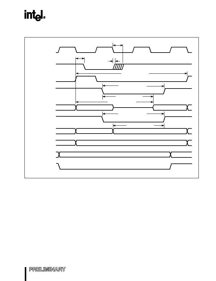
Figure 6. System Bus Timing Diagram (Multiplexed Bus Mode)
CLKOUT
ALE
RD#
AD15:0
(read)
WR#
AD15:0
(write)
BHE#,
INST
AD15:8
TCLCL
Address Out
Data
Data Out
Address Out
Address Out
TCHCL
TLHLL
Valid
A2844-01
TCLLH
TRLCL
TLLCH
TLHLH
TLLRL
TRLRH
TRHLH
TAVLL
TLLAX
TRLDV
TRHDZ
TRLAZ
Address Out
TAVDV
TLLWL
TWLWH
TWHLH
TQVWH
TWHQX
TRHBX
TWHBX
TRHAX
TWHAX
TSLDV
A19:16
CS
x#
Address Out
TWHSH
TRHSH
XTAL1
TXHCH
TXTAL1
8XL196NP COMMERCIAL CHMOS 16-BIT MICROCONTROLLER
25
Figure 7. READY Timing Diagram (Multiplexed Bus Mode)
CLKOUT
READY
ALE
A3250-01
T
CLYX
(min)
T
LHLH
+ 2T
XTAL1
T
AVDV
+ 2T
XTAL1
RD#
AD15:0
(read)
AD15:0
(write)
BHE#, INST
A19:16
CS
x#
T
RLRH
+ 2T
XTAL1
T
AVYV
Data Out
Extended Address Out
Address Out
T
CLYX
(max)
Data In
Address Out
T
RLDV
+ 2T
XTAL1
T
WLWH
+ 2T
XTAL1
T
QVWH
+ 2T
XTAL1
WR#

8XL196NP COMMERCIAL CHMOS 16-BIT MICROCONTROLLER
26
5.3 AC Characteristics -- Demultiplexed Bus Mode
Test Coditions: Capacitive load on all pins = 50 pF, Rise and Fall Times = 3 ns.
Table 12. AC Characteristics, Demultiplexed Bus Mode
Symbol
Parameter
V
CC
= 2.7 V ≠ 3.3 V
Units
Min
Max
The 8XL196NP Will Meet These Specifications
F
XTAL
1
Input requency on XTAL1
8
14
MHz
T
XTAL
1
Period, 1/F
XTAL
1
71
125
ns
T
XHCH
XTAL1 High to CLKOUT High/Low
20
110
ns
T
CLCL
CLKOUT Cycle Time
2T
XTAL
1
ns
T
CHCL
CLKOUT High Period
T
XTAL
1
≠ 10
T
XTAL
1
+ 15
ns
T
AVRL
A19:0, CS
x
# Valid to RD# Low
2T
XTAL
1
≠ 48
ns
T
AVWL
A19:0, CS
x
# Valid to WR# Low
2T
XTAL
1
≠ 37
ns
T
CLLH
CLKOUT Low to ALE High
≠ 12
10
ns
T
LLCH
ALE Low to CLKOUT High
≠ 15
15
ns
T
LHLH
ALE Cycle Time
4T
XTAL
1
ns (1)
T
LHLL
ALE High Period
T
XTAL
1
≠ 12
T
XTAL
1
+ 10
ns
T
RLCH
RD# Low to CLKOUT High
≠ 5
20
ns
T
RLRH
RD# Low Period
2T
XTAL
1
≠ 10
ns (1)
T
RHLH
RD# High to ALE High
T
XTAL
1
≠ 5
T
XTAL
1
+ 20
ns (2)
T
WLCH
WR# Low to CLKOUT High
≠ 10
10
ns
T
QVWH
Data Valid before WR# High
3T
XTAL
1
≠ 55
ns (1)
T
CHWH
CLKOUT High to WR# High
≠ 15
5
ns
T
WLWH
WR# Low Period
2T
XTAL
1
≠ 13
ns (1)
T
WHQX
Data Hold after WR# High
T
XTAL
1
≠ 25
ns
T
WHLH
WR# High to ALE High
T
XTAL
1
≠ 10
T
XTAL
1
+ 20
ns (2)
T
WHBX
BHE#, INST Hold after WR# High
T
XTAL
1
≠ 10
ns
T
WHAX
A19:0, CS
x
# Hold after WR# High
0
ns
T
RHBX
BHE#, INST Hold after RD# High
T
XTAL
1
≠ 10
ns
T
RHAX
A19:0, CS
x
# Hold after RD# High
0
ns
NOTES:
1.
If wait states are used, add 2T
XTAL
1
◊
n
, where
n
= number of wait states.
2.
Assuming back-to-back bus cycles.

8XL196NP COMMERCIAL CHMOS 16-BIT MICROCONTROLLER
27
Table 13. AC Characteristics, Demultiplexed Bus Mode
Symbol
Parameter
V
CC
= 2.7 V ≠ 3.3 V
Units
Min
Max
The External Memory System Must Meet These Specifications
T
AVYV
A19:0, CS
x
# Valid to READY Setup
3T
XTAL
1
≠ 88
ns
T
YLYH
Non READY Time
No Upper Limit
ns
T
CLYX
READY Hold after CLKOUT Low
T
XTAL
1
≠ 30
ns (1)
T
AVDV
A19:0, CS
x
# Valid to Input Data Valid
4T
XTAL
1
≠ 75
ns (2)
T
RLDV
RD# Active to Input Data Valid
2T
XTAL
1
≠ 33
ns (2)
T
CLDV
CLKOUT Low to Input Data Valid
T
XTAL
1
≠ 50
ns
T
RHDZ
End of RD# to Input Data Float
T
XTAL
1
≠ 5
ns
T
RXDX
Data Hold after RD# Inactive
0
ns
NOTES:
1.
Exceeding the maximum specification causes additional wait states.
2.
If wait states are used, add 2T
XTAL
1
◊
n
, where
n
= number of wait states.

8XL196NP COMMERCIAL CHMOS 16-BIT MICROCONTROLLER
28
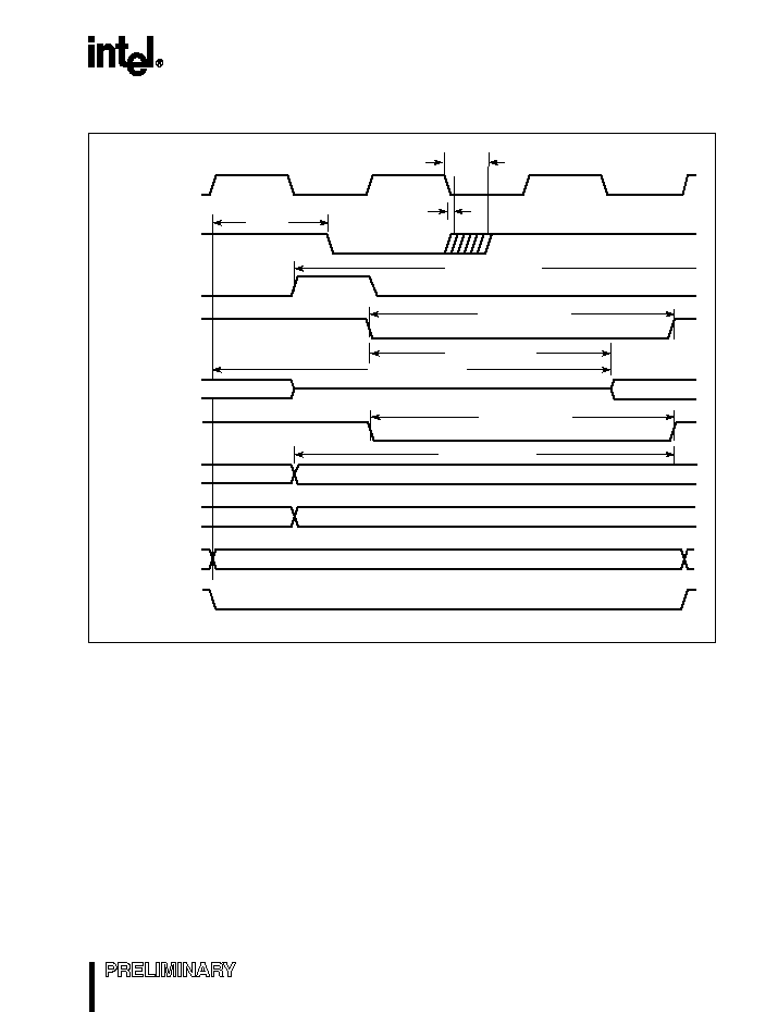
Figure 8. System Bus Timing Diagram (Demultiplexed Bus Mode)
CLKOUT
ALE
RD#
AD15:0
(read)
WR#
AD15:0
(write)
BHE#,
INST
A19:0
CS
x#
TCLCL
Valid
Valid
Address Out
TCHCL
TLHLL
Valid
A2845-01
TCLLH
TCLDV
TLLCH
TLHLH
TRLCH
TRLRH
TRHLH
TRLDV
TRHDZ
TAVDV
TWLCH
TWLWH
TWHLH
TQVWH
TWHQX
TRHBX
TWHBX
TRHAX
TWHAX
TCHWH
Address
XTAL1
TXTAL1
TXHCH
8XL196NP COMMERCIAL CHMOS 16-BIT MICROCONTROLLER
29
Figure 9. READY Timing Diagram (Demultiplexed Bus Mode)
CLKOUT
READY
ALE
A3256-01
AD15:0
(read)
WR#
AD15:0
(write)
BHE#, INST
A19:0
Extended Address Out
T
CLYX
(max)
T
AVYV
Data
T
LHLH
+ 2T
XTAL1
T
RLDV
+ 2T
XTAL1
Data Out
T
QVWH
+ 2T
XTAL1
CS
x
#
T
CLYX
(min)
T
RLRH
+ 2T
XTAL1
RD#
T
WLWH
+ 2T
XTAL1
T
AVDV
+ 2T
XTAL1
8XL196NP COMMERCIAL CHMOS 16-BIT MICROCONTROLLER
30
5.4 HOLD#/HLDA# Timing
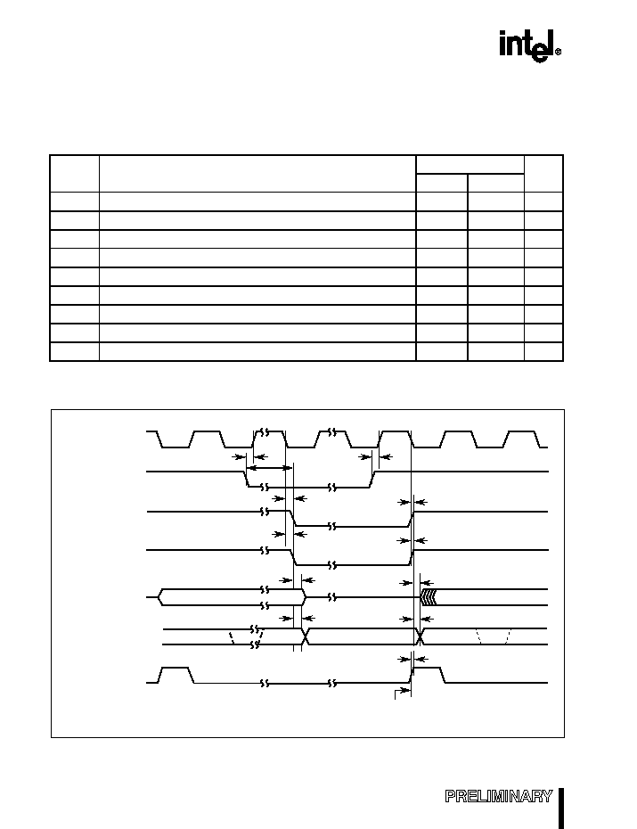
Figure 10. HOLD#/HLDA# Timing Diagram
Table 14. HOLD#/HLDA# Timings
Symbol
Parameter
V
CC
= 2.7 V ≠ 3.3V
Units
Min
Max
T
HVCH
HOLD# Setup Time (to guarantee recognition at next clock)
83
ns
T
CLHAL
CLKOUT Low to HLDA# Low
≠15
15
ns
T
CLBRL
CLKOUT Low to BREQ# Low
≠15
15
ns
T
HALAZ
HLDA# Low to Address Float
33
ns
T
HALBZ
HLDA# Low to BHE#, INST, RD#, WR# Weakly Driven
25
ns
T
CLHAH
CLKOUT Low to HLDA# High
≠25
15
ns
T
CLBRH
CLKOUT Low to BREQ# High
≠25
25
ns
T
HAHAX
HLDA# High to Address No Longer Floating
≠20
ns
T
HAHBV
HLDA# High to BHE#, INST, RD#, WR# Valid
≠20
ns
A2460-03
CLKOUT
HOLD#
HLDA#
BREQ#
A19:0, AD15:0
CS
x#, BHE#,
INST, RD#, WR#
WRL#, WRH#
ALE
T
CLLH
T
CLHAH
T
CLBRH
T
HAHAX
T
HAHBV
T
HALBZ
T
HALAZ
T
CLBRL
T
CLHAL
T
HVCH
T
HVCH
Hold Latency
Start of strongly driven ALE
Weakly held inactive

8XL196NP COMMERCIAL CHMOS 16-BIT MICROCONTROLLER
31
5.5 AC Characteristics -- Serial Port, Shift Register Mode
Figure 11. Serial Port Waveform -- Shift Register Mode
Table 15. Serial Port Timing -- Shift Register Mode
Symbol
Parameter
V
CC
= 2.7 V ≠ 3.3V
Units
Min
Max
T
XLXL
Serial Port Clock period
(BRR
x
002H)
(BRR
=
x
001H) (Note 1)
6T
XTAL
1
4T
XTAL
1
ns
ns
T
QVXH
Output data setup to clock high
3T
XTAL
1
≠ 30
ns
T
XHQX
Output data hold after clock high
2T
XTAL
1
≠ 90
ns
T
XHQV
Next output data valid after clock high
2T
XTAL
1
+ 50
ns
T
DVXH
Input data setup to clock high
2T
XTAL
1
+ 50
ns
T
XHDX
Input data hold after clock high
0
ns
T
XHQZ
Last clock high to output float
5T
XTAL
1
+ 30
ns
NOTE:
1.
The minimum baud-rate register value for receptions is
x
002H and the minimum baud-rate register
value for transmissions is
x
001H.
Valid
Valid
Valid
Valid
Valid
Valid
Valid
Valid
RXD
(In)
(Out)
TXD
0
1
2
3
4
5
6
7
TQVXH
TXLXL
TDVXH
TXHQV
TXHQZ
TXHDX
TXHQX
TXLXH
A2080-02
RXD
8XL196NP COMMERCIAL CHMOS 16-BIT MICROCONTROLLER
32
5.6 External Clock Drive
Figure 12. External Clock Drive Waveforms
5.7 Test Output Waveforms
Figure 13. AC Testing Output Waveforms During 3.0 Volt Testing
Table 16. External Clock Drive
Symbol
Parameter
Min
Max
Units
1/T
XLXL
Input frequency
8
14
MHz
T
XLXL
Period (T
XTAL
1
)
71
125
ns
T
XHXX
High Time
0.35T
XTAL
1
0.65T
XTAL
1
ns
T
XLXX
Low Time
0.35T
XTAL
1
0.65T
XTAL
1
ns
T
XLXH
Rise Time
10
ns
T
XHXL
Fall Time
10
ns
A2119-02
T
XHXX
T
XLXX
T
XHXL
T
XLXL
0.3 V
CC
≠ 0.5 V
0.7 V
CC
+ 0.5 V
T
XLXH
0.7 V
CC
+ 0.5 V
0.3 V
CC
≠ 0.5 V
AC testing inputs are driven at 2.5 V for a logic "1" and 0.25 V for
a logic "0". Timing measurements are made at 1.6 V for a logic
"1" and 0.5 V for a logic "0".
A2740-01
Test Points
1.6 V
0.5 V
2.5 V
0.25 V
1.6 V
0.5 V
8XL196NP COMMERCIAL CHMOS 16-BIT MICROCONTROLLER
33
Figure 14. Float Waveforms During 3.0 Volt Testing
V
LOAD
+ 0.15 V
V
LOAD
≠ 0.15 V
Timing Reference
Points
V
LOAD
V
OH
≠ 0.15 V
V
OL
+ 0.15 V
For timing purposes, a port pin is no longer floating when a
150 mV change from load voltage occurs and begins to float
when a 150 mV change from the loading V
OH
/V
OL
level occurs
with I
OL
/I
OH
10 mA.
A2739-01

8XL196NP COMMERCIAL CHMOS 16-BIT MICROCONTROLLER
34
6.0 THERMAL CHARACTERISTICS
All thermal impedance data is approximate for static
air conditions at 1 watt of power dissipation. Values
will change depending on operating conditions and
the application. The Intel
Packaging Handbook
(order number 240800) describes Intel's thermal
impedance test methodology.
7.0 8XL196NP ERRATA
Change identifiers have been used on embedded
products since 1990. The change identifier is the
last character in the FPO number. The FPO number
is typically a nine character number located on the
second line of the topside package mark. The
following errata listing is applicable to the B≠step
(denoted by a "B" or "C" at the end of the topside
tracking number):
1.
Any jump, conditional jump, or call instruction
located within six bytes of the top of a page,
i.e., 0FFFA≠0FFFFH, may cause a jump to the
wrong page. To ensure this problem does not
occur, place at least six NOPs at the top of
each page.
8.0 DATASHEET REVISION HISTORY
This datasheet is valid for devices with an "A" at the
end of the topside tracking number. Datasheets are
changed as new device information becomes
available. Verify with your local Intel sales office that
you have the latest version before finalizing a
design or ordering devices.
Table 17. Thermal Characteristics
Package Type
JA
JC
100-pin SQFP
55
∞
C/W
14
∞
C/W
100-pin QFP
56
∞
C/W
16
∞
C/W