 | –≠–ª–µ–∫—Ç—Ä–æ–Ω–Ω—ã–π –∫–æ–º–ø–æ–Ω–µ–Ω—Ç: 9863 | –°–∫–∞—á–∞—Ç—å:  PDF PDF  ZIP ZIP |

Datasheet
3
Document #: 249115
Revision #: 003
Rev. Date: 08/07/01
Contents
Contents
1.0
Block Diagram ............................................................................................................................... 7
2.0
Pin Assignments and Signal Descriptions ................................................................................. 8
3.0
Functional Description................................................................................................................ 16
3.1
Introduction ......................................................................................................................... 16
3.2
Port Configuration ............................................................................................................... 17
3.2.1
Auto-Negotiation .................................................................................................... 17
3.2.2
Link Establishment and Port Connection ............................................................... 18
3.3
Interface Descriptions ......................................................................................................... 18
3.3.1
Twisted-Pair Interface ............................................................................................ 18
3.3.2
Media Independent Interface ................................................................................. 18
3.4
Repeater Operation ............................................................................................................ 19
3.4.1
100 Mbps Repeater Operation .............................................................................. 19
3.4.2
10 Mbps Repeater Operation ................................................................................ 20
3.5
Requirements ..................................................................................................................... 20
3.5.1
Power..................................................................................................................... 20
3.5.2
Clock ...................................................................................................................... 21
3.5.3
Bias Resistor.......................................................................................................... 21
3.5.4
Reset ..................................................................................................................... 21
3.5.5
IRB Bus Pull-ups.................................................................................................... 21
3.6
LED Operation .................................................................................................................... 21
3.6.1
LEDs at Start-up .................................................................................................... 21
3.6.2
LED Event Stretching ............................................................................................ 22
3.6.3
Serial LED Interface............................................................................................... 22
3.6.4
Serial Shifting......................................................................................................... 22
3.6.4.1
Serial LED Signals ................................................................................. 23
3.6.4.2
Activity Graph LEDs............................................................................... 23
3.6.5
Direct Drive LEDs .................................................................................................. 24
3.6.6
LED Modes ............................................................................................................ 24
3.6.6.1
LED Mode 1 ........................................................................................... 25
3.6.6.2
LED Mode 2 ........................................................................................... 25
3.6.6.3
LED Mode 3 ........................................................................................... 26
3.6.6.4
LED Mode 4 ........................................................................................... 28
3.7
IRB Operation ..................................................................................................................... 28
3.7.1
IRB Signal Types ................................................................................................... 28
3.7.2
10M-Only Operation .............................................................................................. 29
3.7.2.1
MAC IRB Access ................................................................................... 29
3.7.3
LXT98x/91x/98xx Compatibility ............................................................................. 29
3.8
MII Port Operation .............................................................................................................. 31
3.8.1
Preamble Handling ................................................................................................ 31
4.0
Application Information .............................................................................................................. 32
4.1
General Design Guidelines ................................................................................................. 32
4.2
Power and Ground.............................................................................................................. 33
4.2.1
Supply Filtering ...................................................................................................... 33
4.2.2
Ground Noise......................................................................................................... 33

Contents
4
Datasheet
Document #: 249115
Revision #: 003
Rev. Date: 08/07/01
4.2.3
Power and Ground Plane Layout Considerations.................................................. 33
4.2.4
Chassis Ground ..................................................................................................... 34
4.2.5
The RBIAS Pin....................................................................................................... 34
4.2.6
MII Terminations .................................................................................................... 35
4.2.7
Twisted-Pair Interface............................................................................................ 36
4.2.7.1
Magnetics Information............................................................................ 36
4.2.8
Clock...................................................................................................................... 37
4.2.9
LED Circuits........................................................................................................... 39
4.2.9.1
Direct Drive LEDs .................................................................................. 39
4.2.9.2
LED Pins Multiplexed with Configuration Inputs .................................... 39
4.2.9.3
Serial LEDs ............................................................................................ 40
4.3
Inter-Repeater Backplane Compatibility ............................................................................. 41
4.3.1
Local Backplane--3.3V Only ................................................................................. 41
4.3.2
Stack Backplane--3.3V or 5V ............................................................................... 41
4.3.2.1
3.3V-Only Stacks ................................................................................... 41
4.3.2.2
For 5V Backwards Stackability .............................................................. 41
4.3.2.3
3.3V and 5.0V Stacking Boards Cannot Be Mixed ................................ 41
5.0
Test Specifications...................................................................................................................... 44
6.0
Mechanical Specifications.......................................................................................................... 56
Figures
1
LXT98x3 Block Diagram............................................................................................................... 7
2
LXT9883 Pin Assignments ........................................................................................................... 8
3
Typical LXT9883 Repeater Architecture .................................................................................... 17
4
MII Interface................................................................................................................................ 19
5
Serial LED Shift Loading ........................................................................................................... 22
6
Serial LED Port Signaling ........................................................................................................... 23
7
100M IRB Connection ................................................................................................................ 29
8
IRB Block Diagram .................................................................................................................... 30
9
LXT9883 MII Operation .............................................................................................................. 32
10
Power and Ground Connections ................................................................................................ 35
11
Typical Twisted-Pair Port Interface and Power Supply Filtering ................................................ 38
12
Typical Reset Circuit .................................................................................................................. 38
13
LED Circuits - Direct Drive & Multiplexed Configuration Inputs .................................................. 39
14
Serial LED Circuit ....................................................................................................................... 40
15
100M Backplane Connection between LXT98x and LXT98x3 ................................................... 42
16
Typical 100 Mbps IRB Implementation ...................................................................................... 43
17
Typical 10 Mbps IRB Implementation ........................................................................................ 43
18
100 Mbps TP Port-to-Port Delay Timing..................................................................................... 48
19
100BASE-TX MII-to-TP Port Timing .......................................................................................... 49
20
100BASE-TX TP-to-MII Timing ................................................................................................. 50
21
10BASE-T MII-to-TP Timing ...................................................................................................... 51
22
10BASE-T TP-to-MII Port Timing .............................................................................................. 52
23
100 Mbps TP-to-IRB Timing ...................................................................................................... 53
24
10 Mbps TP-to-IRB Timing ........................................................................................................ 54
25
10 Mbps IRB-to-TP Port Timing ................................................................................................ 55
26
LXT98x3 Package Specifications .............................................................................................. 56

Datasheet
5
Document #: 249115
Revision #: 003
Rev. Date: 08/07/01
Contents
Tables
1
MII #1 Signal Descriptions ............................................................................................................ 9
2
MII #2 Signal Descriptions .......................................................................................................... 10
3
Inter-Repeater Backplane Signal Descriptions ........................................................................... 11
4
Twisted-Pair Port Signal Descriptions ........................................................................................ 13
5
LED Signal Descriptions ............................................................................................................. 14
6
Power Supply and Indication Signal Descriptions ...................................................................... 15
7
Miscellaneous Signal Descriptions ............................................................................................. 16
8
Serial LED Port Bit Stream ......................................................................................................... 23
9
ACTGLED Display Modes .......................................................................................................... 24
10
LED Terms.................................................................................................................................. 24
11
LED Mode 1 Indications.............................................................................................................. 25
12
LED Mode 2 Indications.............................................................................................................. 26
13
LED Mode 3 Indications.............................................................................................................. 27
14
LED Mode 4 Indications.............................................................................................................. 28
15
Cascading and Stacking Connections ........................................................................................ 30
16
IRB Signal Details....................................................................................................................... 31
17
LXT98x3 Magnetics Specifications............................................................................................. 36
18
Oscillator Manufacturers............................................................................................................. 37
19
Absolute Maximum Ratings ........................................................................................................ 44
20
Operating Conditions .................................................................................................................. 44
21
Input System Clock1 Requirements ........................................................................................... 44
22
I/O Electrical Characteristics....................................................................................................... 45
23
100 Mbps IRB Electrical Characteristics..................................................................................... 45
24
10 Mbps IRB Electrical Characteristics....................................................................................... 46
25
100BASE-TX Transceiver Electrical Characteristics ................................................................. 47
26
10BASE-T Transceiver Electrical Characteristics...................................................................... 47
27
100 Mbps TP Port-to-Port Delay Timing Parameters ................................................................. 48
28
100BASE-TX MII-to-TP Port Timing Parameters ....................................................................... 49
29
100BASE-TX TP-to-MII Timing Parameters ............................................................................... 50
30
10BASE-T MII-to-TP Timing Parameters ................................................................................... 51
31
10BASE-T TP-to-MII Port Timing Parameters............................................................................ 52
32
100 Mbps TP-to-IRB Timing Parameters1.................................................................................. 53
33
10 Mbps TP-to-IRB Timing Parameters1.................................................................................... 54
34
10 Mbps IRB-to TP Port Timing Parameters .............................................................................. 55

Contents
6
Datasheet
Document #: 249115
Revision #: 003
Rev. Date: 08/07/01
Revision History
Date
Revision
Page
Description
August 2001
003
44
Modify the Absolute Maximum Ratings Supply Voltage value to 4.0V.
February 2001
002
21, 37
Modified clock requirements language.
21
Replaced TBD value under reset to 3.15V.
33
Replaced TBDs in fourth para under Supply Filtering to 1000 mA and
1500 mA.
36
Replaced TBDs in fourth bullet under Twisted-Pair Interface to 1000
mA and 1500 mA.
37
Modified Oscillator Manufacturers table
43
Typical 100 Mbps IRB Implementation table:
Modified note 2 (replaced "FPS/ = 0" with "FPS/
0."
43
Typical 10 Mbps IRB Implementation table:
Modified note 2 (replaced "FPS/ = 0" with "FPS/
0."
44
Absolute Maximum Ratings table:
Replaced TBD for Supply Voltage under Max to 3.45.
Deleted Operating Temperature lines and values.
44
Operating Conditions table:
For Power Consumption: removed Auto-Negotiation values.
Changed description and values for 8- and 6-port active.
Advanced 10/100 Unmanaged Repeater -- LXT9883/9863
Datasheet
7
Document #: 249115
Revision #: 003
Rev. Date: 08/07/01
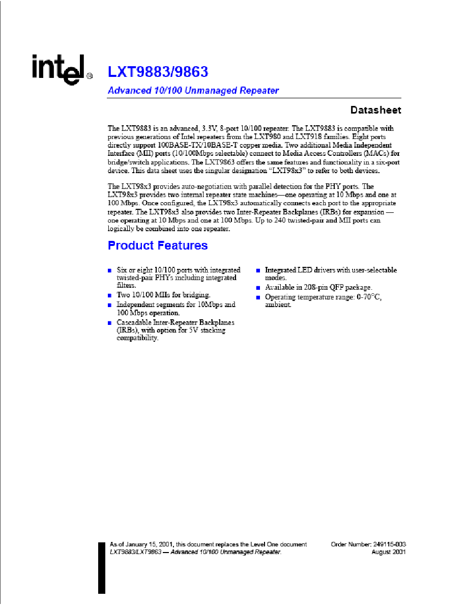
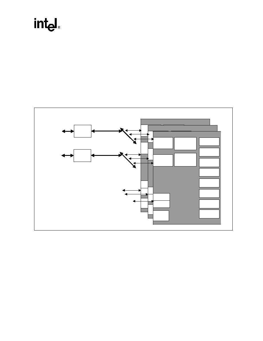
1.0
Block Diagram
Figure 1. LXT98x3 Block Diagram
10BASE-T
Repeater
100BASE-X
Repeater
Serial LED
Drivers
10/100 PHY 1
10 Mbps
Backplane
100 Mbps
Backplane
P
o
r
t
S
w
it
c
h
ing Logic
10M IRB
100M IRB
Port & Mgmt
Status Indicators
TX_I/O
10/100 PHY 2
TX_I/O
10/100 PHY 3
TX_I/O
10/100 PHY 4
TX_I/O
10/100 PHY 5
TX_I/O
10/100 PHY 6
TX_I/O
10/100 PHY 7
TX_I/O
10/100 PHY 8
TX_I/O
MII 1
MII_I/O
MII 2
MII_I/O
LXT9883/9863 -- Advanced 10/100 Unmanaged Repeater
8
Datasheet
Document #: 249115
Revision #: 003
Rev. Date: 08/07/01
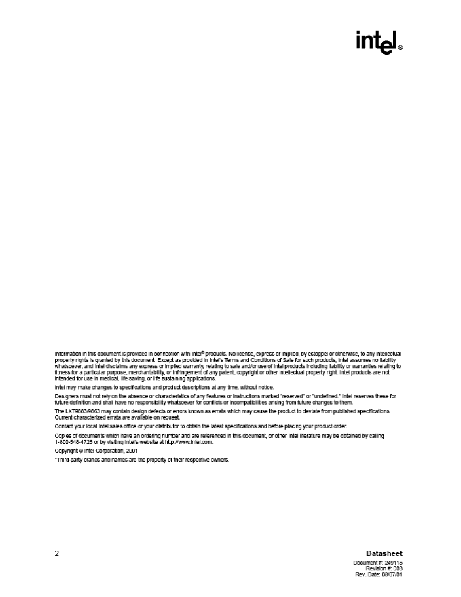
2.0
Pin Assignments and Signal Descriptions
Figure 2. LXT9883 Pin Assignments
Package Topside Markings
Marking
Definition
Part #
LXT9883 is the unique identifier for this product family.
Rev #
Identifies the particular silicon "stepping" (Refer to Specification Update for additional stepping
information.)
Lot #
Identifies the batch.
FPO #
Identifies the Finish Process Order.
5
2
......
.....
N
/
C
5
1
......
.....
N
/
C
5
0
......
.....
IR
1
0
0
C
L
K
4
9
......
.....
IR
1
0
0
D
A
T
4
4
8
......
.....
IR
1
0
0
D
A
T
3
4
7
......
.....
V
C
C
4
6
......
.....
GN
D
4
5
......
.....
IR
1
0
0
D
A
T
2
4
4
......
.....
IR
1
0
0
D
A
T
1
4
3
......
.....
IR
1
0
0
D
A
T
0
4
2
......
.....
IR
100D
V
4
1
......
.....
IR
100D
E
N
4
0
......
.....
IR
100C
O
L
3
9
......
.....
C
O
M
P
_
S
E
L
3
8
......
.....
IR
100S
NG
L
3
7
......
.....
IR
100C
F
S
B
P
3
6
......
.....
IR
100C
F
S
3
5
......
.....
M
I
I1
_
R
X
D
3
3
4
......
.....
M
I
I1
_
R
X
D
2
3
3
......
.....
N
/
C
3
2
.....
.....
M
I
I1
_
R
X
D
1
3
1
......
.....
M
I
I1
_
R
X
D
0
3
0
......
.....
M
I
I1
_
R
X
D
V
2
9
......
.....
M
I
I1
_
R
X
C
L
K
2
8
......
.....
V
C
C
2
7
......
.....
GN
D
2
6
......
.....
M
I
I1
_
R
X
E
R
2
5
......
.....
N
/
C
2
4
......
.....
M
I
I1
_
T
X
E
R
2
3
......
.....
M
I
I1
_
T
X
C
L
K
2
2
......
.....
M
I
I1
_
T
X
E
N
2
1
......
.....
M
I
I1
_
T
X
D
0
2
0
......
.....
M
I
I1
_
T
X
D
1
1
9
......
.....
M
I
I1
_
T
X
D
2
1
8
......
.....
M
I
I2
_
S
P
D
1
7
......
.....
M
I
I1
_
T
X
D
3
1
6
......
.....
V
C
C
1
5
......
.....
GN
D
1
4
......
.....
M
I
I1
_
C
OL
1
3
......
.....
M
I
I1
_
C
R
S
1
2
......
.....
IR
1
0
C
L
K
1
1
......
.....
IR
1
0
D
A
T
1
0
......
.....
IR
1
0
E
N
A
9
.
.
......
.....
M
I
I1
_
S
P
D
8
.
.
......
.....
V
C
C
7
.
.
......
.....
GN
D
6
.
.
......
.....
IR
1
0
D
E
N
5
.
.
......
.....
IR
1
0
C
FS
B
P
4
.
.
......
.....
IR
1
0
C
OL
B
P
3
.
.
......
.....
IR
1
0
C
OL
2
.
.
......
.....
IR
1
0
C
FS
1
.
.
......
.....
GN
D
RESET....... 53
CLK25....... 54
N/C....... 55
N/C....... 56
N/C....... 57
N/C....... 58
N/C....... 59
N/C....... 60
VCC....... 61
GND....... 62
N/C....... 63
N/C....... 64
N/C....... 65
N/C....... 66
N/C....... 67
N/C....... 68
N/C....... 69
N/C....... 70
N/C....... 71
FPS....... 72
N/C....... 73
VCC....... 74
GND....... 75
VCC....... 76
VCC....... 77
RPS_FAULT....... 78
RPS_PRES....... 79
MACACTIVE....... 80
HOLDCOL....... 81
LEDCLK....... 82
LEDDAT....... 83
LEDLAT....... 84
VCC....... 85
GND....... 86
ORT1_LED3....... 87
ORT1_LED2....... 88
ORT1_LED1....... 89
GND....... 90
ORT2_LED3....... 91
ORT2_LED2....... 92
ORT2_LED1....... 93
GND....... 94
ORT3_LED3....... 95
ORT3_LED2....... 96
ORT3_LED1....... 97
GND....... 98
ORT4_LED3....... 99
ORT4_LED2....... 100
ORT4_LED1....... 101
RBIAS....... 102
GND....... 103
TPIP1....... 104
208 ....... MII2_RXD3
207 ....... MII2_RXD2
206 ....... MII2_RXD1
205 ....... MII2_RXD0
204 ....... MII2_RXDV
203 ....... MII2_RXCLK
202 ....... MII2_RXER
201 ....... N/C
200 ....... VCC
199 ....... GND
198 ....... N/C
197 ....... MII2_TXER
196 ....... MII2_TXCLK
195 ....... MII2_TXEN
194 ....... MII2_TXD0
193 ....... MII2_TXD1
192 ....... MII2_TXD2
191 ....... MII2_TXD3
190 ....... VCC
189 ....... GND
188 ....... MII2_COL
187 ....... MII2_CRS
186 ....... COL100_LED
185 ....... LEDSEL1/COL10_LED
184 ....... LEDSEL0/ACT100_LED
183 ....... AUTOBLINK/ACT10_LED
182 ....... N/C
181 ....... GND
180 ....... VCC
179 ....... GND
178 ....... N/C
177 ....... VCC
176 ....... PORT8_LED1*
175 ....... PORT8_LED2*/LEDABGSEL
174 ....... PORT8_LED3*
173 ....... VCC
172 ....... GND
171 ....... PORT7_LED1*
170 ....... PORT7_LED2*
169 ....... PORT7_LED3*
168 ....... GND
167 ....... PORT6_LED1
166 ....... PORT6_LED2
165 ....... PORT6_LED3
164 ....... GND
163 ....... PORT5_LED1
162 ....... PORT5_LED2
161 ....... PORT5_LED3
160 ....... TxSLEW_1
159 ....... TxSLEW_0
158 .......GND
157 .......*TPIP8
TP
IN
1
.....
..1
0
5
VC
C
R
.....
..1
0
6
TP
OP
1
.....
..1
0
7
TP
O
N
1
.....
..1
0
8
G
N
D
.....
..1
0
9
TP
O
N
2
.....
..1
1
0
TP
OP
2
.....
..1
1
1
VC
C
T
.....
..1
1
2
VC
C
R
.....
..1
1
3
TP
IN
2
.....
..1
1
4
TP
IP
2
.....
..1
1
5
G
N
D
.....
..1
1
6
G
N
D
.....
..1
1
7
TP
IP
3
.....
..1
1
8
TP
IN
3
.....
..1
1
9
VC
C
R
.....
..1
2
0
TP
OP
3
.....
..1
2
1
TP
O
N
3
.....
..1
2
2
G
N
D
.....
..1
2
3
TP
O
N
4
.....
..1
2
4
TP
OP
4
.....
..1
2
5
VC
C
T
.....
..1
2
6
VC
C
R
.....
..1
2
7
TP
IN
4
.....
..1
2
8
TP
IP
4
.....
..1
2
9
G
N
D
.....
..1
3
0
G
N
D
.....
..1
3
1
TP
IP
5
.....
..1
3
2
TP
IN
5
.....
..1
3
3
VC
C
R
.....
..1
3
4
VC
C
T
.....
..1
3
5
TP
OP
5
.....
..1
3
6
TP
O
N
5
.....
..1
3
7
G
N
D
.....
..1
3
8
TP
O
N
6
.....
..1
3
9
TP
OP
6
.....
..1
4
0
VC
C
R
.....
..1
4
1
TP
IN
6
.....
..1
4
2
TP
IP
6
.....
..1
4
3
G
N
D
.....
..1
4
4
G
N
D
.....
..1
4
5
*
T
P
I
P
7
.....
..1
4
6
*
T
P
I
N
7
.....
..1
4
7
VC
C
R
.....
..1
4
8
VC
C
T
.....
..1
4
9
*
T
P
O
P
7
.....
..1
5
0
*
T
P
O
N
7
.....
..1
5
1
G
N
D
.....
..1
5
2
*
T
P
O
N
8
.....
..1
5
3
*
T
P
O
P
8
.....
..1
5
4
VC
C
R
.....
..1
5
5
*
T
P
I
N
8
.....
..1
5
6
* Indicates LXT9883-only pins. TP Ports 7 and 8 are not available on LXT9863
LXT9883 XX
XXXXXX
XXXXXXXX
Part #
LOT #
FPO #
Part #
LOT #
FPO #
Rev #

Advanced 10/100 Unmanaged Repeater -- LXT9883/9863
Datasheet
9
Document #: 249115
Revision #: 003
Rev. Date: 08/07/01
Table 1. MII #1 Signal Descriptions
Pin
Symbol
Type
1, 2
Description
9
MII1_SPD
I
PU
Speed Select - MII 1. This signal is sensed at power up, hardware reset, and
software reset. Selects operating speed of the respective MII (MAC) interface.
High = 100 Mbps. Low = 10 Mbps.
31
32
34
35
MII1_RXD0
MII1_RXD1
MII1_RXD2
MII1_RXD3
O
Receive Data - MII 1. The LXT98x3 transmits received data to the controller on these
outputs. Data is driven on the falling edge of MII1_RXCLK.
30
MII1_RXDV
O
Receive Data Valid - MII 1. Active High signal, synchronous to MII1_RXCLK,
indicates valid data on MII1_RXD<3:0>.
29
MII1_RXCLK
O
Receive Clock - MII 1. MII receive clock for expansion port. This is a 2.5 or 25 MHz
clock derived from the CLK25 input (refer to
Table 7 on page 16
).
26
MII1_RXER
O
Receive Error - MII 1. Active High signal, synchronous to MII1_RXCLK, indicates
invalid data on MII1_RXD<3:0>.
24
MII1_TXER
I
Transmit Error - MII 1. MII1_TXER is a 100M-only signal. The MAC asserts this
input when an error has occurred in the transmit data stream. The LXT98x3 responds
by sending `Invalid Code Symbols' on the line.
23
MII1_TXCLK
O
Transmit Clock - MII 1. This is a 2.5 or 25 MHz clock derived from the CLK25 input
(refer to
Table 7 on page 16
).
22
MII1_TXEN
I
Transmit Enable - MII 1. External controllers drive this input High to indicate data is
transmitted on the MII1_TXD<3:0> pins. Ground this input if unused.
21
20
19
17
MII1_TXD0
MII1_TXD1
MII1_TXD2
MII1_TXD3
I
Transmit Data - MII 1. External controllers use these inputs to transmit data to the
LXT98x3. The LXT98x3 samples MII1_TXD<3:0> on the rising edge of MII1_TXCLK,
when MII1_TXEN is High.
14
MII1_COL
O
Collision - MII 1. The LXT98x3 drives this signal High to indicate a collision
occurred.
13
MII1_CRS
O
Carrier Sense - MII 1. Active High signal indicates LXT98x3 is transmitting or
receiving.
1. I = Input, O = Output, I/O = Input/Output, D = Digital, A = Analog, AI = Analog Input, A I/O = Analog Input/Output, OD = Open
Drain,
OS = Open Source, PD = Pull Down, PU = Pull Up.
NC = No Clamp. Pad does not clamp input in the absence of power.
2. Pins are 5V tolerant, unless indicated.

LXT9883/9863 -- Advanced 10/100 Unmanaged Repeater
10
Datasheet
Document #: 249115
Revision #: 003
Rev. Date: 08/07/01
Table 2. MII #2 Signal Descriptions
Pin
Symbol
Type
1, 2
Description
18
MII2_SPD
I
PU
Speed Select - MII 2. This signal is sensed at power up, hardware reset, and
software reset. Selects operating speed of the respective MII (MAC) interface.
High = 100 Mbps. Low = 10 Mbps.
205
206
207
208
MII2_RXD0
MII2_RXD1
MII2_RXD2
MII2_RXD3
O
Receive Data - MII 2. The LXT98x3 transmits received data to the controller on these
outputs. Data is driven on the falling edge of MII2_RXCLK.
204
MII2_RXDV
O
Receive Data Valid - MII 2. Active High signal, synchronous to MII2_RXCLK,
indicates valid data on MII2_RXD<3:0>.
203
MII2_RXCLK
O
Receive Clock - MII 2. MII receive clock for expansion port. This is a 2.5 or 25 MHz
clock derived from the CLK25 input (refer to
Table 7 on page 16
).
202
MII2_RXER
O
Receive Error - MII 2. Active High signal, synchronous to MII2_RXCLK, indicates
invalid data on MII2_RXD<3:0>.
197
MII2_TXER
I
Transmit Error - MII 2. MII2_TXER is a 100M-only signal. The MAC asserts this
input when errors occurs in the transmit data stream. The LXT98x3 sends `Invalid
Code Symbols' on the line.
196
MII2_TXCLK
O
Transmit Clock - MII 2. This is a 2.5 or 25 MHz clock derived from the CLK25 input
(refer to
Table 7 on page 16
).
195
MII2_TXEN
I
Transmit Enable - MII 2. External controllers drive this input High to indicate data is
transmitted on the MII2_TXD<3:0> pins. Ground this input if unused.
194
193
192
191
MII2_TXD0
MII2_TXD1
MII2_TXD2
MII2_TXD3
I
Transmit Data - MII 2. External controllers use these inputs to transmit data to the
LXT98x3. The LXT98x3 samples MII2_TXD<3:0> on the rising edge of MII2_TXCLK,
when MII2_TXEN is High.
188
MII2_COL
O
Collision - MII 2. The LXT98x3 drives this signal High to indicate a collision
occurred.
187
MII2_CRS
O
Carrier Sense - MII 2. Active High signal indicates LXT98x3 is transmitting or
receiving.
1. I = Input, O = Output, I/O = Input/Output, D = Digital, A = Analog, AI = Analog Input, A I/O = Analog Input/Output, OD = Open
Drain,
OS = Open Source, PD = Pull Down, PU = Pull Up.
NC = No Clamp. Pad does not clamp input in the absence of power.
2. Pins are 5V tolerant, unless indicated.

Advanced 10/100 Unmanaged Repeater -- LXT9883/9863
Datasheet
11
Document #: 249115
Revision #: 003
Rev. Date: 08/07/01
Table 3. Inter-Repeater Backplane Signal Descriptions
Pin
Symbol
Type
1, 2
Description
Common IRB Signals
39
COMP_SEL
AI
Compatibility Mode Select. 3.3V on this pin causes the IRCFSBP signals to operate in
3.3V only mode. 5V on this pin causes the IR100CFSBP or IR10CFSBP signals to
operate in 5V backwards compatibility mode with LXT98x devices.
100 Mbps IRB Signals
36
IR100CFS
3
A I/O
OD
100 Mbps IRB Collision Force Sense. A three-level signal that determines number of
active ports on the "logical" repeater. High level (3.3V) indicates no ports active; Mid
level (approx. 1.6V) indicates one port active; Low level (0V) indicates more than one
port active, resulting in a collision. This signal requires a 215
pull-up resistor, and
connects between ICs on the same board.
37
IR100CFSBP
A I/O
OD
100 Mbps IRB Collision Force Sense - Backplane. This three-level signal functions
the same as IR100CFS; however, it connects between ICs with FPS = 0, on different
boards. IR100CFSBP requires a single 91
pull-up resistor in each stack. This signal
can be set in either 5V or 3.3V modes by the COMP_SEL pin.
38
IR100SNGL
I/O
Schmitt PU
100 Mbps Single Driver State. This active Low signal is asserted by the device with
FPS = 0 when a packet is received from one or more ports. Do not connect this signal
between boards.
40
IR100COL
I/O
Schmitt PU
100 Mbps Multiple Driver State. This active Low signal is asserted by the device with
FPS = 0 when a packet is being received from more than one port (collision). Do not
connect this signal between boards.
41
IR100DEN
O
OD
100 Mbps IRB Driver Enable. This output provides directional control for an external
bidirectional transceiver (74LVT245) used to buffer the 100 Mbps IRB in multi-board
applications. It must be pulled up by a 330
resistor. When there are multiple devices
on one board, tie all IR100DEN outputs together. If IR100DEN is tied directly to the DIR
pin on a 74LVT245, attach the on-board IR100DAT, IR100CLK, and IR100DV signals to
the "B" side of the 74LVT245, and connect the off-board signals to the "A" side of the
74LVT245.
42
IR100DV
I/O
Schmitt
OD
PU
100 Mbps IRB Data Valid. This active Low signal indicates port activity on the
repeater. IR100DV frames the clock and data of the packet on the backplane. This
signal requires a 300
pull-up resistor.
43
44
45
48
49
IR100DAT0
IR100DAT1
IR100DAT2
IR100DAT3
IR100DAT4
I/O
Tri-state
Schmitt
PU
100 Mbps IRB Data. These bidirectional signals carry 5-bit data on the 100 Mbps IRB.
Data is driven on the falling edge and sampled on the rising edge of IR100CLK. Buffer
these signals between boards.
50
IR100CLK
I/O
Tri-state
Schmitt
PD
100 Mbps IRB Clock. This bidirectional, non-continuous, 25 MHz clock is recovered
from received network traffic. Schmitt triggering is used to increase noise immunity. This
signal must be pulled to VCC when idle. One 1 k
pull-up resistor on both sides of a
74LVT245 buffer is recommended.
1. I = Input, O = Output, I/O = Input/Output, D = Digital, AI = Analog Input, A I/O = Analog Input/Output, OD = Open Drain,
OS = Open Source, PD = Pull Down, PU = Pull Up. Even if the IRB is not used, required pull-up resistors must be installed as
listed above.
NC = No Clamp. Pad does not clamp input in the absence of power.
2. Pins are 5V tolerant, unless indicated.
3. IR100CFS is not 5V tolerant.
4. IR10CFS is not 5V tolerant.
LXT9883/9863 -- Advanced 10/100 Unmanaged Repeater
12
Datasheet
Document #: 249115
Revision #: 003
Rev. Date: 08/07/01
10 Mbps IRB Signals
11
IR10DAT
I/O
OD
PD
10 Mbps IRB Data. This bidirectional signal carries data on the 10 Mbps IRB. Data is
driven and sampled on the rising edge of the corresponding IRCLK. This signal must be
pulled High by a 330
resistor. Buffer this signal between boards.
12
IR10CLK
I/O
Tri-state
Schmitt
PD
10 Mbps IRB Clock. This bidirectional, non-continuous, 10 MHz clock is recovered
from received network traffic. During idle periods, the output is high-impedance. Schmitt
triggering is used to increase noise immunity.
6
IR10DEN
O
OD
10 Mbps IRB Driver Enable. This output provides directional control for an external
bidirectional transceiver (74LVT245) used to buffer the IRBs in multi-board applications.
It must be pulled up by a 330
resistor. When there are multiple devices on one board,
tie all IR10DEN outputs together. If IR10DEN is tied directly to the DIR pin on a
74LVT245, attach the on-board IR10DAT, IR10CLK and IR10ENA signals to the "B" side
of the 74LVT245, and connect the off-board signals to the "A" side of the 74LVT245.
10
IR10ENA
I/O
OD
PU
10 Mbps IRB Enable. This active Low output indicates carrier presence on the IRB. A
330
pull-up resistor is required to pull the IR10ENA output High when the IRB is idle.
When there are multiple devices, tie all IR10ENA outputs together. Buffer these
signals between boards.
3
IR10COL
I/O
OD
PU
10 Mbps IRB Collision. This output is driven Low to indicate a collision occurred on the
10 Mbps segment. A 330
resistor is required on each board to pull this signal High
when there is no collision. Do not connect between boards and do not buffer.
4
IR10COLBP
I/O
OD
10 Mbps IRB Collision - Backplane. This active Low output has the same function as
IR10COL, but is used between boards. Attach this signal only from the device with FPS
= 0 to the backplane or connector, without buffering. The output must be pulled up by
one 330
resistor per stack.
2
IR10CFS
4
A, I/O
OD
10 Mbps IRB Collision Force Sense. This three-state analog signal indicates transmit
collision when driven Low. IR10CFS requires a 215
, 1% pull-up resistor. Do not
connect this signal between boards and do not buffer.
5
IR10CFSBP
A I/O
OD
Note: 10 Mbps IRB Collision Force Sense - Backplane. Functions the same as
IR10CFS, but connects between boards. Attach this signal only from the device
with FPS = 0 to the backplane or connector, without buffering. This signal
requires one 330
, 1% pull-up resistor per stack. This signal can be set for 5V or
3.3V modes by the COMP_SEL pin.
80
MACACTIVE
I
PD
Note: MAC Active. Active High input allows external ASICs to participate in 10 Mbps
IRB. Driving data onto the IRB requires the external ASIC assert MACACTIVE
High for one clock cycle, then assert IR10ENA Low. ASIC monitors IR10COL
(active Low) for collision. By using MACACTIVE, the repeater--not the MAC--
drives the three-level IR10CFS pin.
81
HOLDCOL
I/O
PD
Note: Hold Collision for 10 Mbps mode. This active High signal is driven by the
device with FPS = 0 to extend a non-local transmit collision to other devices on
the same board. Do not attach the HOLDCOL signals from different boards
together.
Table 3. Inter-Repeater Backplane Signal Descriptions (Continued)
Pin
Symbol
Type
1, 2
Description
1. I = Input, O = Output, I/O = Input/Output, D = Digital, AI = Analog Input, A I/O = Analog Input/Output, OD = Open Drain,
OS = Open Source, PD = Pull Down, PU = Pull Up. Even if the IRB is not used, required pull-up resistors must be installed as
listed above.
NC = No Clamp. Pad does not clamp input in the absence of power.
2. Pins are 5V tolerant, unless indicated.
3. IR100CFS is not 5V tolerant.
4. IR10CFS is not 5V tolerant.

Advanced 10/100 Unmanaged Repeater -- LXT9883/9863
Datasheet
13
Document #: 249115
Revision #: 003
Rev. Date: 08/07/01
Table 4. Twisted-Pair Port Signal Descriptions
Pin
Symbol
Type
1
Description
107, 108
111, 110
121, 122
125, 124
136, 137
140, 139
150, 151
154, 153
TPOP1, TPON1
TPOP2, TPON2
TPOP3, TPON3
TPOP4, TPON4
TPOP5, TPON5
TPOP6, TPON6
TPOP7, TPON7
TPOP8, TPON8
Caution: AO
Twisted-Pair Outputs - Ports 1 through 8. These pins are the positive and
negative outputs from the respective ports' twisted-pair line drivers. For unused
ports, these pins can be left open.
104, 105
115, 114
118, 119
129, 128
132, 133
143, 142
146, 147
157, 156
TPIP1, TPIN1
TPIP2, TPIN2
TPIP3, TPIN3
TPIP4, TPIN4
TPIP5, TPIN5
TPIP6, TPIN6
TPIP7, TPIN7
TPIP8, TPIN8
Caution: AI
Twisted-Pair Inputs - Ports 1 through 8. These pins are the positive and
negative inputs to the respective ports' twisted-pair receivers.
For unused ports, tie together with 100
resistors and float.
160
159
TxSLEW_1
TxSLEW_0
I
PD
Tx Output Slew Controls 0 and 1. These pins select the TX output slew rate
(rise and fall time) as follows:
TxSLEW_1
TxSLEW_0
Slew Rate (Rise and Fall Time)
0
0
2.5 ns
0
1
3.1 ns
1
0
3.7 ns
1
1
4.3 ns
1. I = Input, O = Output, I/O = Input/Output, D = Digital, A = Analog, AI = Analog Input, AO = Analog Output, A I/O = Analog
Input/Output,
OD = Open Drain,
OS = Open Source, PD = Pull Down, PU = Pull Up.
NC = No Clamp. Pad does not clamp input in the absence of power.

LXT9883/9863 -- Advanced 10/100 Unmanaged Repeater
14
Datasheet
Document #: 249115
Revision #: 003
Rev. Date: 08/07/01
Table 5. LED Signal Descriptions
Pin
Symbol
Type
1, 2
Description
184
185
LEDSEL0
LEDSEL1
I
3
O - OD/OS
LED Mode Select - Input. See Note 3 in footer below.
00 = Mode 1, 01 = Mode 2, 10 = Mode 3, 11 = Mode 4
These pins are shared with the LEDACT100, LEDCOL10 outputs.
175
LEDABGSEL
I
3
O - OD/OS
LED Activity Bar Graph Mode Select - Input. See Note 2 in footer below.
0 = Base-10 Mode, 1 = Base-2 Mode
Refer to
"Activity Graph LEDs" on page 23.
This pin is shared with the Port8_LED2 output.
183
AUTOBLINK
I
3
O - OD/OS
LED Blink Mode Select - Input. See Note 3 in footer below.
0 = Auto blink on, 1 = Auto blink off
This pin is shared with the LEDACT100, LEDCOL10 outputs.
83
LEDDAT
O
LED Data. Serial data stream that is shifted into external Serial-to-Parallel
LED drivers. See
"Serial LED Interface" on page 22..
84
LEDLAT
O
LED Latch. Parallel load clock for external Serial-to-Parallel LED drivers.
See
"Serial LED Interface" on page 22..
82
LEDCLK
O
LED Clock. Serial data stream clock for external Serial-to-Parallel LED
drivers. See
"Serial LED Interface" on page 22..
176
171
167
163
101
97
93
89
PORT8_LED1
PORT7_LED1
PORT6_LED1
PORT5_LED1
PORT4_LED1
PORT3_LED1
PORT2_LED1
PORT1_LED1
O
OD
LED Driver 1 - Ports 1 through 8. Programmable LED driver. Active Low.
See
"Direct Drive LEDs" on page 24..
Port8_LED1 must be pulled High via a 100≠500 k
resistor if LED circuit
not used.
175
170
166
162
100
96
92
88
PORT8_LED2
PORT7_LED2
PORT6_LED2
PORT5_LED2
PORT4_LED2
PORT3_LED2
PORT2_LED2
PORT1_LED2
O
OD
LED Driver 2 - Ports 1 through 8. Programmable LED driver. Active Low.
See
"Direct Drive LEDs" on page 24..
The Port8_LED2 pin is shared with the LEDABGSEL configuration input.
174
169
165
161
99
95
91
87
PORT8_LED3
PORT7_LED3
PORT6_LED3
PORT5_LED3
PORT4_LED3
PORT3_LED3
PORT2_LED3
PORT1_LED3
O
OD
LED Driver 3 - Ports 1 through 8. Programmable LED driver. Active Low.
See
"Direct Drive LEDs" on page 24..
Port8_LED3 must be pulled High via a 100≠500 k
resistor if LED circuit
not used.
185
COL10_LED
I
O - OD/OS
10M Collision LED Driver. Active output indicates collision on 10M
segment. This pin is shared with the LEDSEL1 configuration input.
1. I = Input, O = Output, I/O = Input/Output, D = Digital, A = Analog, AI = Analog Input, A I/O = Analog Input/Output, OD = Open
Drain,
OS = Open Source, PD = Pull Down, PU = Pull Up. Even if the IRB is not used, required pull-up resistors must be installed as
listed above.
NC = No Clamp. Pad does not clamp input in the absence of power.
2. Pins are 5V tolerant, unless indicated.
3. Input must be static; Refer to
"LED Pins Multiplexed with Configuration Inputs" on page 39.
for information on pin use.

Advanced 10/100 Unmanaged Repeater -- LXT9883/9863
Datasheet
15
Document #: 249115
Revision #: 003
Rev. Date: 08/07/01
186
COL100_LED
I
O - OD/OS
100M Collision LED Driver. Active output indicates collision on 100M
segment.
183
ACT10_LED
I
O - OD/OS
10M Activity LED Driver. Active output indicates activity on 10M segment.
This pin is shared with the AUTOBLINK configuration input (refer to Note 3
below).
184
ACT100_LED
I
O - OD/OS
100M Activity LED Driver. Active output indicates activity on 100M
segment. This pin is shared with the LEDSEL0 configuration input (refer to
Note 3 below).
Table 6. Power Supply and Indication Signal Descriptions
Pin
Symbol
Type
1, 2
Description
8, 16, 28,
47, 61, 74,
76, 77, 85,
173, 177,
180, 190,
200
VCC
-
Power Supply Inputs. Each of these pins must be connected to a common
+3.3 VDC power supply. A de-coupling capacitor to digital ground should be
supplied for every one of these pins.
106, 113,
120, 127,
134, 141,
148, 155
VCCR
-
Analog Supply Inputs - Receive. Each of these pins must be connected to a
common +3.3 VDC power supply. A de-coupling capacitor to GND should be
supplied for every one of these pins. Use ferrite beads to create a separate
analog VCC plane.
112, 126,
135, 149
VCCT
-
Analog Supply Inputs - Transmit. Each of these pins must be connected to a
common +3.3 VDC power supply. A de-coupling capacitor to GND should be
supplied for every one of these pins. Use ferrite beads to create a separate
analog VCC plane.
1, 7, 15, 27,
46, 62, 75,
86, 90, 94,
98, 103,
109, 116,
117, 123,
130, 131,
138, 144,
145, 152,
158, 164,
168, 172,
179, 181,
189, 199
GND
-
Ground. Connect each of these pins to system ground plane.
1. I = Input, O = Output, I/O = Input/Output, D = Digital, A = Analog, AI = Analog Input, A I/O = Analog Input/Output, OD = Open
Drain,
OS = Open Source, PD = Pull Down, PU = Pull Up.
NC = No Clamp. Pad does not clamp input in the absence of power.
2. Pins are 5V tolerant, unless indicated.
Table 5. LED Signal Descriptions (Continued)
Pin
Symbol
Type
1, 2
Description
1. I = Input, O = Output, I/O = Input/Output, D = Digital, A = Analog, AI = Analog Input, A I/O = Analog Input/Output, OD = Open
Drain,
OS = Open Source, PD = Pull Down, PU = Pull Up. Even if the IRB is not used, required pull-up resistors must be installed as
listed above.
NC = No Clamp. Pad does not clamp input in the absence of power.
2. Pins are 5V tolerant, unless indicated.
3. Input must be static; Refer to
"LED Pins Multiplexed with Configuration Inputs" on page 39.
for information on pin use.

LXT9883/9863 -- Advanced 10/100 Unmanaged Repeater
16
Datasheet
Document #: 249115
Revision #: 003
Rev. Date: 08/07/01
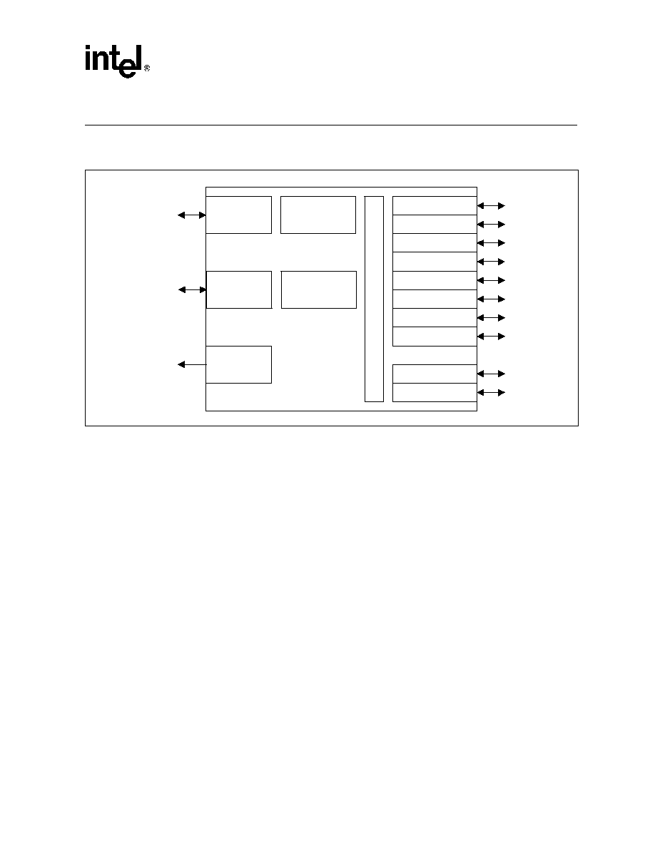
3.0
Functional Description
3.1
Introduction
As a fully integrated IEEE 802.3 compliant repeater capable of 10 Mbps and 100 Mbps operation,
the LXT98x3 is a versatile device allowing great flexibility in Ethernet design solutions.
Figure 3
shows a typical application. Refer to
"Application Information" on page 32.
for specific circuit
implementations.
102
RBIAS
A
RBIAS. Used to provide bias current for internal circuitry. The 100
µ
A bias
current is provided through an external 22.1 k
,
1%
resistor to GND.
79
RPS_PRES
I
PD
Redundant Power Supply Present. Active High input indicates presence of
redundant power supply. Tie Low if not used.
78
RPS_FAULT
I
PU
Redundant Power Supply Fault. Active Low input indicates redundant power
supply fault. The state of this input is reflected in the RPS_LED output (refer to
LED section). Tie High if not used.
Table 7. Miscellaneous Signal Descriptions
Pin
Symbol
Type
1, 2
Description
53
RESET
I
Schmitt
Reset. This active Low input causes internal circuits, state machines and
counters to reset (address tracking registers do not reset). On power-up,
devices should not be brought out of reset until the power supply stabilizes to
3.3V. When there are multiple devices, it is recommended all be supplied by
a common reset driven by an `LS14 or similar device.
54
CLK25
I
Schmitt
25 MHz system clock. Refer to
Table 21 on page 44.
72
FPS
I
TTL
First Position Select. In multi-chip configurations, this pin identifies one
device on each board that drives the HOLDCOL signal to extend non-local
collisions to other devices on the board. Set Low for first device on the PCB.
Set High for all other devices on the PCB.
25, 33, 51, 52,
55-60, 63-71,
73, 178, 182,
198, 201
N/C
-
No Connects. Leave these pins unconnected.
1. I = Input, O = Output, I/O = Input/Output, D = Digital, A = Analog, AI = Analog Input, A I/O = Analog Input/Output, OD = Open
Drain,
OS = Open Source, PD = Pull Down, PU = Pull Up.
NC = No Clamp. Pad does not clamp input in the absence of power.
2. Pins are 5V tolerant, unless indicated.
Table 6. Power Supply and Indication Signal Descriptions (Continued)
Pin
Symbol
Type
1, 2
Description
1. I = Input, O = Output, I/O = Input/Output, D = Digital, A = Analog, AI = Analog Input, A I/O = Analog Input/Output, OD = Open
Drain,
OS = Open Source, PD = Pull Down, PU = Pull Up.
NC = No Clamp. Pad does not clamp input in the absence of power.
2. Pins are 5V tolerant, unless indicated.
Advanced 10/100 Unmanaged Repeater -- LXT9883/9863
Datasheet
17
Document #: 249115
Revision #: 003
Rev. Date: 08/07/01
This multi-port repeater provides six (LXT9863) or eight (LXT9883) 10BASE-T/100BASE-TX
ports. In addition, each device also provides two Media Independent Interface (MII) expansion
ports that may be connected to 10/100 MACs.
The LXT98x3 provides two repeater state machines and two Inter-Repeater Backplanes (IRB) on a
single chip--one for 10 Mbps and one for 100 Mbps operation. The 100 Mbps repeater meets IEEE
802.3 Class II requirements. The auto-negotiation capability of the LXT98x3 allows it to
communicate with connected nodes and configure itself accordingly.
The segmented backplane simplifies dual-speed operation, and allows multiple devices to be
stacked and function as one logical Class II repeater. Up to 240 ports (192 TP ports and 48 MII
ports) can be supported in a single stack.
3.2
Port Configuration
The LXT98x3 powers up in auto-negotiation mode for all twisted-pair ports.
3.2.1
Auto-Negotiation
All TP ports on power-up are configured to establish link via auto-negotiation. The port and link
partner establish link conditions by exchanging Fast Link Pulse (FLP) bursts. Each FLP burst
contains 16 bits of data advertising the port's capabilities. If the link partner does not support auto-
negotiation, the LXT98x3 determines link state by listening for 100 Mbps IDLE symbols or 10
Mbps link pulses. If it detects either of these signals, it configures the port accordingly.
Figure 3. Typical LXT9883 Repeater Architecture
LXT9883 IC
Device
Management
10BASE-T
Repeater
100BASE-
X
Repeater
LED
Drivers
RMON &
SNMP
Counters
10 Mbps
Backplane
100 Mbps
Backplane
10/100
PHY
10/100
PHY
MII
MII
10/100
PHY
10/100
PHY
10/100
PHY
10/100
PHY
10/100
PHY
10/100
PHY
LXT9883 IC
Device
Management
10BASE-T
Repeater
100BASE-
X
Repeater
LED
Drivers
RMON &
SNMP
Counters
10 Mbps
Backplane
100 Mbps
Backplane
10/100
PHY
10/100
PHY
MII
MII
10/100
PHY
10/100
PHY
10/100
PHY
10/100
PHY
10/100
PHY
10/100
PHY
LXT9883 IC
10BASE-T
Repeater
100BASE-X
Repeater
LED
Drivers
10 Mbps
Backplane
100 Mbps
Backplane
10/100
PHY
10/100
PHY
MII
MII
10/100
PHY
10/100
PHY
10/100
PHY
10/100
PHY
10/100
PHY
10/100
PHY
Buffer
100M
Ba
ckp
la
n
e
100M Backplane
Buffer
10M Backplane
MII to MII Bridge
10M
Ba
ckp
la
n
e

LXT9883/9863 -- Advanced 10/100 Unmanaged Repeater
18
Datasheet
Document #: 249115
Revision #: 003
Rev. Date: 08/07/01
3.2.2
Link Establishment and Port Connection
Once a port establishes link, the LXT98x3 automatically connects it to the appropriate repeater
state machine. If link loss is detected and auto-negotiation is enabled, the port returns to the auto-
negotiation state.
3.3
Interface Descriptions
The LXT9883 and LXT9863 provide eight and six network interface ports, respectively. Each port
is a twisted-pair interface that directly supports 100BASE-TX (100TX) and 10BASE-T (10T)
Ethernet applications and fully complies with IEEE 802.3 standards. A common termination circuit
is used.
3.3.1
Twisted-Pair Interface
The LXT98x3 pinout is optimized for dual-height RJ-45 connectors. The twisted-pair interface for
each port consists of two differential signal pairs -- one for transmit and one for receive. The
transmit signal pair is TPOP/TPON, the receive signal pair is TPIP/TPIN.
The transmitter requires magnetics with 1:1 turns ratio. The center tap of the primary side of the
transmit winding must be tied to a quiet VCC for proper operation.
The receiver requires magnetics with a 1:1 turns ratio, and a load of 100
. When the twisted-pair
port is enabled, the receiver actively biases its inputs to approximately 2.8V. A 4 k
load is always
present across the TPIP/TPIN pair.
When used in 100TX applications, the LXT98x3 sends and receives a continuous, scrambled
125 Mbps MLT-3 waveform on this interface. In the absence of data, IDLE symbols are sent and
received in order to maintain the link.
When used in 10T applications, the LXT98x3 sends and receives a non-continuous, 10 Mbps
Manchester-encoded waveform. To maintain link during idle periods, the LXT98x3 sends link
pulses every 16 ms, and expects to receive them every 10 to 20 ms. Each 10T port automatically
detects and sends link pulses, and disables its transmitter if link pulses are not detected. Each
10BASE-T port can detect and automatically correct for polarity reversal on the TPIP/N inputs.
The 10BASE-T interface provides integrated filters using Intel's patented filter technology. These
filters facilitate low-cost stack designs to meet EMI requirements.
3.3.2
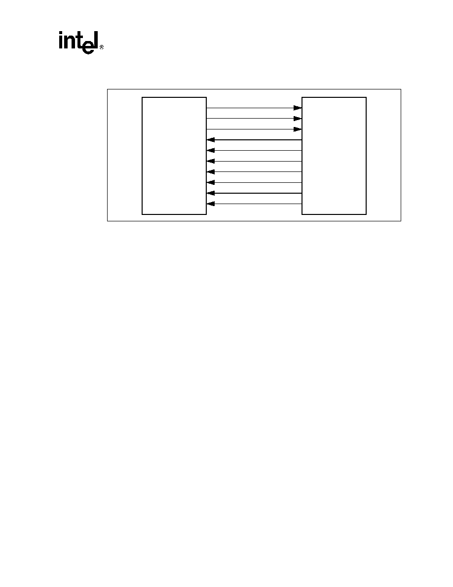
Media Independent Interface
The LXT98x3 has two identical MII interfaces. The MII has been designed to allow expansion to a
Media Access Controller (MAC) as shown in
Figure 4
. This interface is not MDIO/MDC capable.
These MII ports can be set via hardware tie ups/downs to be either 10 Mbps or 100 Mbps. These
ports are not the full MII drive strength and are intended only for point-to-point links.
Advanced 10/100 Unmanaged Repeater -- LXT9883/9863
Datasheet
19
Document #: 249115
Revision #: 003
Rev. Date: 08/07/01
3.4
Repeater Operation
The LXT98x3 contains two internal repeater state machines -- one operating at 10 Mbps and the
other at 100 Mbps. The LXT98x3 automatically switches each port to the correct repeater, once the
operational state of that port has been determined. Each repeater connects all ports configured to
the same speed (including the MII), and the corresponding Inter-Repeater Backplane. Both
repeaters perform the standard jabber and partition functions.
3.4.1
100 Mbps Repeater Operation
The LXT98x3 contains a complete 100 Mbps Repeater State Machine (100RSM) that is fully IEEE
802.3 Class II compliant. Any port configured for 100 Mbps operation is automatically connected
to the 100 Mbps Repeater. This includes any of the eight media and two MII ports configured for
100 Mbps operation.
The 100 Mbps RSM has its own Inter-Repeater Backplane (100IRB). Multiple LXT98x3s can be
cascaded on the 100IRB and operate as one repeater segment. Data from any port is forwarded to
all other ports in the cascade. The 100IRB is a 5-bit symbol-mode interface. It is designed to be
stackable.
The LXT98x3 performs the following 100 Mbps repeater functions:
∑
Signal amplification, wave-shape restoration, and data-frame forwarding.
∑
SOP, SOJ, EOP, EOJ delay < 46BT; class II compliant.
∑
Collision Enforcement. During a 100 Mbps collision, the LXT98x3 drives a 0101 jam signal
(encoded as Data 5 on TX links) to all ports until the collision ends. There is no minimum
enforcement time.
∑
Partition. The LXT98x3 partitions any port that participates in excess of 60 consecutive
collisions or one long collision approximately 575.2
µ
s long. Once partitioned, the LXT98x3
monitors and transmits to the port, but does not repeat data received from the port until it un-
partitions.
Figure 4. MII Interface
MAC
TXD(3:0)
TXEN
TXER
TXCLK
RXCLK
LXT98x3
RXD(3:0)
RX_DV
RX_ER
CRS
COL

LXT9883/9863 -- Advanced 10/100 Unmanaged Repeater
20
Datasheet
Document #: 249115
Revision #: 003
Rev. Date: 08/07/01
∑
Un-partition. The un-partition algorithm, which complies with IEEE specification 802.3aa, un-
partitions a port on either transmit or receive of at least 450-560 bits without collision.
∑
Isolate. The LXT98x3 isolates any port receiving more than two successive false carrier
events. A false carrier event is a packet that does not start with a /J/K symbol pair.
∑
Un-isolate. The LXT98x3 un-isolates a port that remains in the IDLE state for 33000 +/- 25%
BT or that receives a valid frame at least 450-500 BT in length.
∑
Jabber. The LXT98x3 ignores any receiver remaining active for more than 57,500 bit times.
The LXT98x3 exits this state when either one of the following conditions is met:
-- On power-up reset
-- When carrier is no longer detected
3.4.2
10 Mbps Repeater Operation
The LXT98x3 contains a complete 10 Mbps Repeater State Machine (10RSM) that is fully IEEE
802.3 compliant. Any port configured for 10 Mbps operation is automatically connected to the
10 Mbps Repeater. This includes any of the media and MII ports configured for 10 Mbps operation.
The 10RSM has its own Inter-Repeater Backplane (10IRB). Multiple LXT98x3s can be cascaded
on the 10IRB and operate as one repeater segment. Data from any port is forwarded to all other
ports in the cascade.
The LXT98x3 performs the following 10 Mbps repeater functions:
∑
Signal amplification, wave-shape restoration, and data-frame forwarding.
∑
Preamble regeneration. All outgoing packets have a minimum 56-bit preamble and 8-bit SFD.
∑
SOP, SOJ, EOP, EOJ delays meet IEEE 802.3 section 9.5.5 and 9.5.6 requirements.
∑
Collision Enforcement. During a 10 Mbps collision, the LXT98x3 drives a jam signal
("1010") to all ports for a minimum of 96 bit times until the collision ends.
∑
Partition. The LXT98x3 partitions any port in excess of 31 consecutive collisions. Once
partitioned, the LXT98x3 continues monitoring and transmitting to the port, but does not
repeat data received from the port until it properly un-partitions. (Also partitions for excessive
collision length.)
∑
Un-partition. The algorithm, which complies with the IEEE 802.3 specification, un-partitions
a port when data can be either received or transmitted from the port for 450-560 bit times
without a collision on that port.
∑
Jabber. The LXT98x3 asserts a minimum-IFG idle period when a port transmits for longer
than 40,000 to 75,000 bit times.
3.5
Requirements
3.5.1
Power
The LXT98x3 has four types of +3.3V power supply input pins: two digital (VCC, GND) and two
analog (VCCR, VCCT). These inputs may be supplied from a single source. Ferrite beads should
be used to separate the analog and digital planes. These supplies should be clean.

Advanced 10/100 Unmanaged Repeater -- LXT9883/9863
Datasheet
21
Document #: 249115
Revision #: 003
Rev. Date: 08/07/01
Each supply input should be decoupled to ground. Refer to
Table 6 on page 15
for power and
ground pin assignments, and to the
"General Design Guidelines" on page 32.
.
3.5.2
Clock
A stable, external 25MHz reference clock source (TTL) is required to the CLK25 pin. The
reference clock is used to generate transmit signals and recover receive signals. A crystal-based
clock is recommended over a derived clock (i.e., PLL-based) to minimize transmit jitter. Refer to
Table 18 on page 37
for a list of recommended oscillators and to
Table 21 on page 44
for clock
timing requirements.
3.5.3
Bias Resistor
The RBIAS input requires a 22.1 k
, 1% resistor connected to ground.
3.5.4
Reset
At power-up, the reset input must be held Low until VCC reaches at least 3.15V. A buffer should be
used to drive reset if there are multiple LXT98x3 devices. The clock must be active.
3.5.5
IRB Bus Pull-ups
Even when the LXT98x3 is used in a stand-alone configuration, pull-up resistors are required on
the IRB signals. See
Figure 16
and
Figure 17 on page 43
.
3.6
LED Operation
The LXT98x3 drives the most commonly used LEDs directly (see
"Direct Drive LEDs" on
page 24.
). The less frequently used LEDs are optionally driven via a serial bus to inexpensive
Serial-to-Parallel devices (see "Serial LEDs" on this page).
3.6.1
LEDs at Start-up
For approximately 2 seconds after the LXT98x3 is reset, all LEDs are driven to the ON state. This
start-up routine is an LED check.
100 Mbps IRB
10 Mbps IRB
IR100CFS
IR10DAT
IR100CFSBP
IR10ENA
IR100DV
IR10COL
IR100CLK
IR10CFS
IR10COLBP
IR10CFSBP
LXT9883/9863 -- Advanced 10/100 Unmanaged Repeater
22
Datasheet
Document #: 249115
Revision #: 003
Rev. Date: 08/07/01
3.6.2
LED Event Stretching
Short lived LED status events are stretched so they may be observed by the human eye. Refer to the
LED1, 2, 3 Modes section for stretching specifics.
3.6.3
Serial LED Interface
The LXT98x3 provides a serial interface to drive additional LEDs via external 8-bit Serial-to-
Parallel converters. A maximum of 30 LEDs can be driven, using four S/P devices. Collision10/
100, Activity10/100 status indications are output on multiplexed configuration pins and are
duplicated on the Serial Port (see
"LED Pins Multiplexed with Configuration Inputs" on page 39.
).
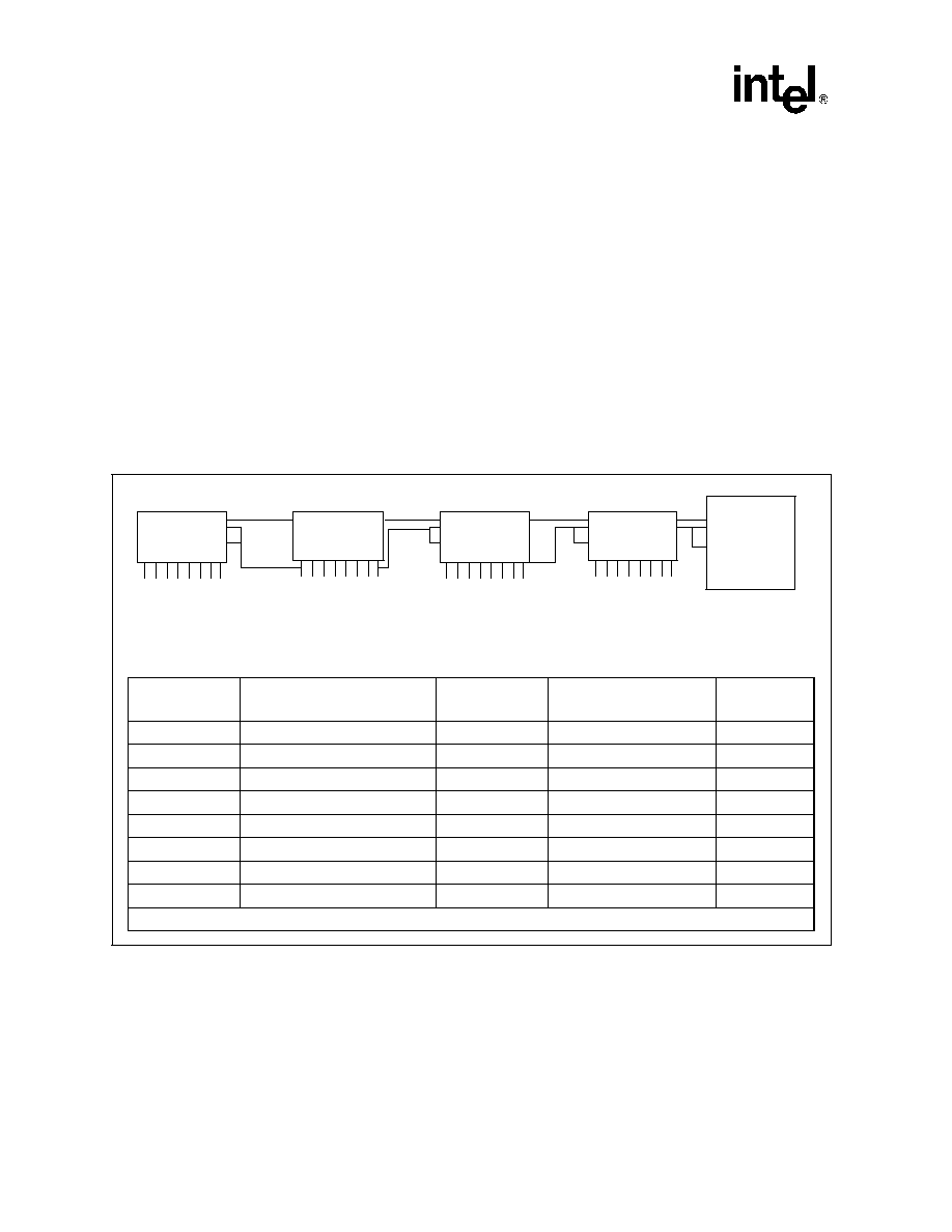
3.6.4
Serial Shifting
Figure 5
shows the Serial LED shift loading.
Figure 5. Serial LED Shift Loading
74X164
74X164
74X164
74X164
2
LXT98x3
MII
Misc
ACT10
ACT100
3
1
4
8
5
7
6
MII
1, 2, 3
Misc
Activity
10M
Activity
100M
Shift Order
MII1 LED1
Collision 10M
ACTG8
ACTG8
8
MII1 LED2
Collision 100M
ACTG7
ACTG7
7
MII1 LED3
Not Used
ACTG6
ACTG6
6
MII2 LED1
Activity 10M
ACTG5
ACTG5
5
MII2 LED2
Activity 100M
ACTG4
ACTG4
4
MI2 LED3
Global Fault
ACTG3
ACTG3
3
Not Used
Not Used
ACTG2
ACTG2
2
Not Used
RPS Fault
ACTG1
ACTG1
1
30 LEDs

Advanced 10/100 Unmanaged Repeater -- LXT9883/9863
Datasheet
23
Document #: 249115
Revision #: 003
Rev. Date: 08/07/01
3.6.4.1
Serial LED Signals
The LED serial interface bus consists of three LXT98x3 outputs: clock (LEDCLK), parallel load
clock (LEDLAT), and output data (LEDDAT). Refer to
Table 5 on page 14
for signal descriptions
and to
Figure 14 on page 40
for an illustration of the LED serial interface circuit. Refer to
Figure 6
and
Table 8
for details on the LED serial bit stream.
3.6.4.2
Activity Graph LEDs
The ACTGLED10 and ACTGLED100 LEDs are for activity bar graphing. The activity
information is integrated and updated over a period of 328.125ms, which has the effect of
smoothing out the activity. LEDs are provided for both the 10 Mbps and 100 Mbps segments.
Figure 6. Serial LED Port Signaling
Table 8. Serial LED Port Bit Stream
Bit
MII Ports-LED1, 2, 3
Misc.
ACTGLED10
ACTGLED100
7
MII Port 1 - LED1
Collision - 10M
1
ACTG8
ACTG8
6
MII Port 1 - LED2
Collision - 100M
1
ACTG7
ACTG7
5
MII Port 1 - LED3
Not Used
ACTG6
ACTG6
4
MII Port 2 - LED1
Activity - 10M
1
ACTG5
ACTG5
3
MII Port 2 - LED2
Activity - 100M
1
ACTG4
ACTG4
2
MII Port 2 - LED3
Global Fault
ACTG3
ACTG3
1
Not Used
Not Used
ACTG2
ACTG2
0
Not Used
RPS Fault
ACTG1
ACTG1
1. These LEDs are multiplexed with Configuration Inputs.
LEDDAT
MII PORTS-LED1,2,3
Misc. LEDs
ACTGLED10
ACTGLED100
Time
LEDLAT
LEDDAT
LEDLAT
b0
b1
b2
b3
b4
b5
b6
b7
LEDCLK
Qa'-Qh' (`595)
Qa-Qh (`164)
b0, b7-b1
b1, b0, b7-b2
b2-b0, b7-b3
b3-b0, b7-b4
b4-b0, b7-b5
b5-b0, b7-b6
b6-b0, b7
b7-b0
b7-b0
Qa-Qh
(`595)
b7-b0
b7-b0
LEDDAT
LEDLAT
LEDCLK
122
µ
s
100 ns / 10 MHz
LXT9883/9863 -- Advanced 10/100 Unmanaged Repeater
24
Datasheet
Document #: 249115
Revision #: 003
Rev. Date: 08/07/01
There are two display modes for the activity bar graphs, Base-2 and Base-10. The modes are
selected via the LEDABGSEL pin. Refer to
Table 9
for details. Each step LED on the bar graph is
lit when the percent activity value associated with that step is met or exceeded.
3.6.5
Direct Drive LEDs
The LXT98x3 provides three direct drive LEDs for each port (PORTn_LED1:3), excluding the two
MII ports. Four additional segment LEDs indicate Collision 10/100 and Activity 10/100.) The per-
port LEDs are updated simultaneously to illustrate clear, non-overlapping status.
The following device pins are multifunctional (input = configuration; output = LED driver):
COL10_LED (185), ACT10_LED (183), ACT100_LED (184), and, PORT8_LED2 (175).
The drive level is determined by the particular input configuration function of the respective pin.
Collision and Activity indications for both 10M and 100M segments are available in both serial
and direct drive.
3.6.6
LED Modes
The four available LED modes are described in
Table 11 - Table 15
. Hardware pins provide global
LED mode control. Refer to
Table 5 on page 14
for pin assignments and signal description.
Table
10
defines terms used to describe LED operation.
Table 9. ACTGLED Display Modes
LED
LEDABGSEL = 0
(Base-10)
LEDABGSEL = 1
(Base-2)
ACTG 8
60+% Activity
80+% Activity
ACTG 7
50% Activity
64% Activity
ACTG 6
40% Activity
32% Activity
ACTG 5
30% Activity
16% Activity
ACTG 4
20% Activity
8% Activity
ACTG 3
10% Activity
4% Activity
ACTG 2
5% Activity
2% Activity
ACTG 1
1% Activity
1% Activity
Table 10. LED Terms
Term
Definition
Port_Enabled
True if port is enabled.
Link_OK
True if link is enabled and link is detected. Always true for MII port.
Port_Partitioned
True if port has been auto partitioned (10Mb mode).
True if port has been auto partitioned or isolated (100Mb mode).
Port_Is_TP
True if port is a twisted-pair port.
RPS_Present
True if redundant power supply is switched in.
RPS_Fault
True if redundant power supply has a fault.
Rcv_Activity
True if twisted-pair port on this device is receiving a packet.
Advanced 10/100 Unmanaged Repeater -- LXT9883/9863
Datasheet
25
Document #: 249115
Revision #: 003
Rev. Date: 08/07/01
3.6.6.1
LED Mode 1
Mode 1 operations are described in
Table 11
.
3.6.6.2
LED Mode 2
Mode 2 operations are described in
Table 12
.
Table 11. LED Mode 1 Indications
LED
Operating Mode
Hardware Control
1
On
Blink
Off
PORTnLED1
10 Mbps operation
Link_OK, not
Port_Partitioned
N/A
Any other state
100 Mbps operation
PORTnLED2
10 Mbps operation
Link_OK,
Port_Partitioned
100 Mbps operation
PORTnLED3
AUTOBLINK active
100M
Link_OK
Not Link_OK
(Fast Blink)
10M Link_OK
AUTOBLINK inactive
N/A
Collision and
Activity LEDs
Any
The collision and activity LEDs are on a Per Segment basis. Pulse
stretchers are used to extend the on-time for the LEDs. For every on-
cycle of the stretched LEDs, an off-cycle, with the same period as the
on-cycle, always follows.
The collision LEDs turn on for approximately 120
µ
s when the
LXT98x3 detects a collision on the segments. During the time that the
LED is on, any additional collisions are ignored by the collision LED
logic.
The activity LEDs turn on for approximately 4 ms when the LXT98x3
detects any activity on the segments. During the time that the LED is
on any additional activity is ignored by the activity LED logic.
On
Blink
Off
Global
Fault
Any
Any Port_Partitioned
or
RPS_Fault and
RPS_Present
N/A
Any other state
RPS Fault
Any
RPS_Present,
RPS_Fault
1. Refer to
Table 11
: LED Terms, which defines all key terms used in this section.

LXT9883/9863 -- Advanced 10/100 Unmanaged Repeater
26
Datasheet
Document #: 249115
Revision #: 003
Rev. Date: 08/07/01
3.6.6.3
LED Mode 3
Mode 3 operations are described in
Table 13
.
Table 12. LED Mode 2 Indications
LED
Operating
Mode
Hardware Control
1
On
Blink
Off
PORTnLED1
Any
10M: Port_Enabled,
Link_OK, not
Port_Partitioned
100M: Port_Enabled,
Link_OK, not
Port_Partitioned
10M: Port_Enabled,
Link_OK, and
Port_Partitioned (slow
blink)
100M: Port_Enabled,
Port_Partitioned
(Slow Blink)
Any other state
PORTnLED2
Rcv_Activity
(20 ms pulse)
2
N/A
Any other state
PORTnLED3
AUTOBLINK active
100M Link_OK
No Link_OK
(Fast Blink)
10M Link_OK
AUTOBLINK inactive
N/A
Collision and
Activity LEDs
Any
The collision and activity LEDs are on a Per Segment basis. Pulse
stretchers are used to extend the on-time for the LEDs. For every on-
cycle of the stretched LEDs, an off-cycle, with the same period as the on-
cycle, always follows.
The collision LEDs turn on for approximately 120
µ
s when the LXT98x3
detects a collision on the segments. During the time that the LED is on,
any additional collisions are ignored by the collision LED logic.
The activity LEDs turn on for approximately 4 ms when the LXT98x3
detects any activity on the segments. During the time that the LED is on,
any additional activity is ignored by the activity LED logic.
RPS Fault
Any
PRS_Present, no
RPS_Fault
PRS_Present,
RPS_Fault
(Slow Blink)
Not RPS_Present
Global Fault
Any
N/A
Any Port_Partitioned,
any Port Isolated
or
RPS_Fault and
RPS_Present
(Slow Blink)
Any other state
1. Refer to
Table 10
: LED Terms, which defines all key terms used in this section.
2. Receive activity is stretched to a 20 ms wide pulse. For every on-cycle of the stretched LEDs, an off-cycle, with the same
period as the on-cycle, always follows.
Advanced 10/100 Unmanaged Repeater -- LXT9883/9863
Datasheet
27
Document #: 249115
Revision #: 003
Rev. Date: 08/07/01
Table 13. LED Mode 3 Indications
LED
Operating Mode
Hardware Control
On
Blink
Off
PORTnLED1
10 Mbps operation
Link_OK, not
Port_Partitioned
N/A
Any other state
100 Mbps operation
PORTnLED2
Any
Rcv_Activity
(20 ms pulse)
2
N/A
Any other state
PORTnLED3
AUTOBLINK active
100M Link_OK
No Link_OK
(Fast Blink)
10M Link_OK
AUTOBLINK inactive
100M mode selected
N/A
10M mode selected
Collision and
Activity LEDs
Any
The collision and activity LEDs are on a Per Segment basis. Pulse
stretchers are used to extend the on-time for the LEDs. For every on-
cycle of the stretched LEDs, an off-cycle, with the same period as the on-
cycle, always follows.
The collision LEDs turn on for approximately 120
µ
s when the LXT98x3
detects a collision on the segments. During the time that the LED is on,
any additional collisions is ignored by the collision LED logic.
The activity LEDs turn on for approximately 4 ms when the LXT98x3
detects any activity on the segments. During the time that the LED is on,
any additional activity is ignored by the activity LED logic.
Global Fault
Any
Any Port_Partitioned
or
RPS_Fault and
RPS_Present
N/A
Any other state
RPS Fault
Any
RPS_Present,
RPS_Fault
1. Refer to
Table 10
: LED Terms, which defines all key terms used in this section.
2. Receive activity is stretched to a 20 ms wide pulse. For every on-cycle of the stretched LEDs, an off-cycle, with the same
period as the on-cycle, always follows.

LXT9883/9863 -- Advanced 10/100 Unmanaged Repeater
28
Datasheet
Document #: 249115
Revision #: 003
Rev. Date: 08/07/01
3.6.6.4
LED Mode 4
Mode 4 operations are described in
Table 14
.
3.7
IRB Operation
The Inter-Repeater Backplane (IRB) allows multiple devices to operate as a single logical repeater,
exchanging data and collision status information. Each segment on the LXT98x3 has its own
complete, independent IRB. The backplanes use a combination of digital and analog signals as
shown in
Figure 8 on page 30
.
3.7.1
IRB Signal Types
IRB signals can be characterized by the following connection types (For Stacking and Cascading
connections, see
Table 15 on page 30
):
∑
Local--connected between devices on the same board
∑
Stack--connected between boards
∑
Full--connected between devices in the same board and between boards.
Table 14. LED Mode 4 Indications
LED
Operating Mode
Hardware Control
1
On
Blink
Off
PORTnLED1
10 Mbps operation
Link_OK, not Port_Partitioned
20 ms Blink
indicates
Rcv_Activity
2
Any other state
100 Mbps operation
Any other state
PORTnLED2
10 Mbps operation
Link_OK, Port_Partitioned
N/A
Any other state
100 Mbps operation
PORTnLED3
AUTOBLINK active
100M Link_OK
No Link_OK
(Fast Blink))
10M Link_OK
AUTOBLINK inactive
N/A
Collision and
Activity LEDs
Any
The collision and activity LEDs are on a Per Segment basis. Pulse
stretchers are used to extend the on-time for the LEDs. For every on-cycle
of the stretched LEDs, an off-cycle, with the same period as the on-cycle,
always follows.
The collision LEDs turn on for approximately 120
µ
s when the LXT98x3
detects a collision on the segments. During the time that the LED is on, any
additional collisions are ignored by the collision LED logic.
The activity LEDs turns on for approximately 4 ms when the LXT98x3
detects any activity on the segments. During the time that the LED is on,
any additional activity is ignored by the activity LED logic.
Global
Fault
Any
Any port partitioned or
RPS_Fault and
RPS_ Present
N/A
Any other state
RPS Fault
Any
RPS_Fault and
RPS_ Present
1. Refer to
Table 10
: LED Terms, which defines all key terms used in this section.
2. Receive activity is stretched to a 20 ms wide pulse. For every on-cycle of the stretched LEDs, an off-cycle, with the same
period as the on-cycle, always follows.
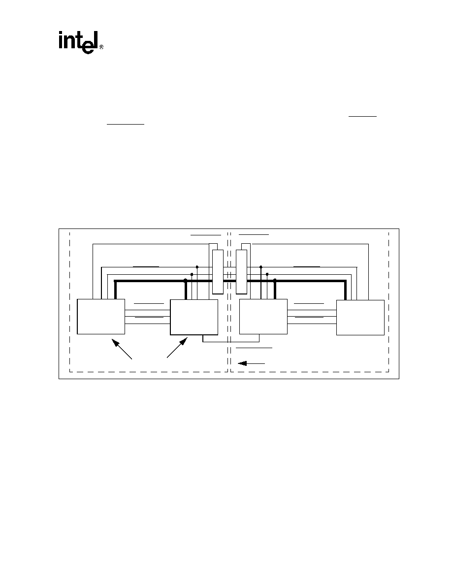
Advanced 10/100 Unmanaged Repeater -- LXT9883/9863
Datasheet
29
Document #: 249115
Revision #: 003
Rev. Date: 08/07/01
3.7.2
10M-Only Operation
3.7.2.1
MAC IRB Access
The MACACTIVE pin allows an external MAC or other digital ASIC to interface directly to the
10 Mbps IRB. When the MACACTIVE pin is asserted, the LXT98x3 drives the IR10CFS and
IR10CFSBP signals on behalf of the external device, allowing it to participate in collision detection
functions.
3.7.3
LXT98x/91x/98xx Compatibility
The LXT98x3 devices feature low-power 3.3V design. The LXT98x and LXT91x devices operate
at 5V and are incompatible with the LXT98x3 devices in cascades. The LXT98x3 devices,
however, are backwards stackable with LXT98x and LXT91x repeaters.
Refer to
"Inter-Repeater Backplane Compatibility" on page 41.
.
Figure 7. 100M IRB Connection
IR100DAT(4:0)
IR100DV
IR100CLK
IR100CFS
IR100DAT(4:0)
IR100DV
IR100CLK
IR100CFSBP
HUB #1
HUB #2
74L
V
T
24
5
74L
V
T
24
5
IR100DEN
IR100DEN
IR100SNGL
IR100COL
IR100CFS
IR100SNGL
IR100COL
LXT98x3
LXT98x3
(0)
LXT98x3
(0)
LXT98x3
Cascade
Stack
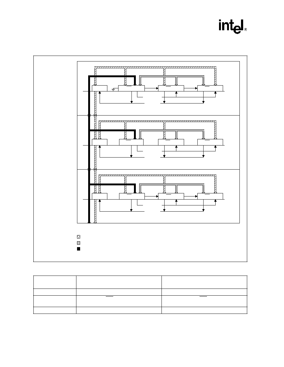
LXT9883/9863 -- Advanced 10/100 Unmanaged Repeater
30
Datasheet
Document #: 249115
Revision #: 003
Rev. Date: 08/07/01
Figure 8. IRB Block Diagram
Table 15. Cascading and Stacking Connections
Signal Type
Connections Between Devices
(Cascading)
Connections Between Boards
(Stacking)
Local
Connect all.
Do not connect.
Stack
For devices with FPS = 0, pull-up at each device
and do not interconnect.
Connect devices with FPS = 0 between boards.
Use one pull-up resistor per stack.
Full
Connect all.
Connect using buffers.
Digital IRB signals include IRnDAT, IRnCOL, IR10COLBP, IRnENA and IRnCLK.
Local Analog IRB signal: IRnCFS.
Inter-Board Analog IRB signal: IRnCFSBP.
This diagram shows a single IRB. The LXT98x3 actually has two independent IRBs, one per speed/segment.
'245
FPS = 0
FPS = 1
FPS = 1
Hub Board 1
Digital IRB Signals
Analog IRB Signals
IRDEN
HOLDCOL
'245
FPS = 0
FPS = 1
FPS = 1
Hub Board 2
Digital IRB Signals
Analog IRB Signals
IRDEN
HOLDCOL
'245
FPS = 0
FPS = 1
FPS = 1
Hub Board n
Digital IRB Signals
Analog IRB Signals
IRDEN
HOLDCOL
HOLDCOL is used on the 10Mbps IRB Only.

Advanced 10/100 Unmanaged Repeater -- LXT9883/9863
Datasheet
31
Document #: 249115
Revision #: 003
Rev. Date: 08/07/01
3.8
MII Port Operation
The LXT98x3 MII ports allow direct connection with a MAC. The MII ports can operate at either
10 Mbps or 100 Mbps. Speed control is provided via MIIn_SPD. For 100 Mbps operation, set
MIIn_SPD = 1. For 10 Mbps operation, set MIIn_SPD = 0.
3.8.1
Preamble Handling
When operating at 100 Mbps, the LXT98x3 passes the full 56 bits of preamble through before
sending the SFD. When operating at 10 Mbps, the LXT98x3 sends data across the MII starting
with the 8-bit SFD (no preamble bits).
Table 16. IRB Signal Details
Name
Pad Type
Buffer
Pull-up
Connection Type
100 Mbps IRB Signals
IR100DAT<4:0>
Digital
Yes
No
Full
IR100CLK
Digital
Yes
1K
Full
IR100DV
Digital, Open Drain
Yes
300
Full
IR100CFS
Analog
No
215
, 1%
Local
IR100CFSBP
Analog
No
91
, 1%
Stack
IR100COL
Digital
No
No
Local
IR100SNGL
Digital
No
No
Local
IR100DEN
Digital, Open Drain
N/A
1
330
Local
10 Mbps IRB Signals
IR10DAT
Digital, Open Drain
Yes
330
Full
IR10CLK
Digital
Yes
No
Full
IR10ENA
Digital, Open Drain
Yes
330
Full
IR10CFS
Analog
No
215
, 1%
Local
IR10CFSBP
Analog
No
330
, 1%
Stack
IR10COL
Digital
No
330
, 1%
Local
IR10COLBP
Digital
No
330
, 1%
Stack
IR10DEN
Digital, Open Drain
N/A
1
330
Local
1. Driver Enable signals are provided to control an external bidirectional transceiver.

LXT9883/9863 -- Advanced 10/100 Unmanaged Repeater
32
Datasheet
Document #: 249115
Revision #: 003
Rev. Date: 08/07/01
4.0
Application Information
4.1
General Design Guidelines
Following generally accepted design practices is essential to minimize noise levels on power and
ground planes. Up to 50mV of noise is considered acceptable. 50mV to 80mV of noise is
considered marginal. High-frequency switching noise can be reduced, and its effects can be
eliminated, by following these simple guidelines throughout the design:
∑
Fill in unused areas of the signal planes with solid copper. Attach them with vias to a VCC or
ground plane that is not located adjacent to the signal layer.
∑
Use ample bulk and decoupling capacitors throughout the design (a .01
µ
F value is
recommended for decoupling caps).
∑
Provide ample power and ground planes.
∑
Provide termination on all high-speed switching signals and clock lines.
∑
Provide impedance matching on long traces to prevent reflections.
∑
Route high-speed signals next to a continuous, unbroken ground plane.
∑
Filter and shield DC-DC converters, oscillators, etc.
∑
Do not route any digital signals between the LXT98x3 and the RJ-45 connectors at the edge of
the board.
∑
Do not extend any circuit power and ground plane past the center of the magnetics or to the
edge of the board. Use this area for chassis ground, or leave it void.
Figure 9. LXT9883 MII Operation
MIIn_TXD<3:0>
MIIn_TXEN
MIIn_TXER
MIIn_TXCLK
MIIn_RXCLK
MIIn_RXD<3:0>
MIIn_RXDV
MIIn_RXER
MIIn_CRS
MIIn_COL
LXT9883
10/100
MAC
Port 1
Port 2
Port 3
Port 4
Ports 1, 2
TP Ports
MII Ports
Port 6
Port 7
Port 8
Port 5
The two LXT9883 MII ports act
as the PHY side of the MII. An
external MAC sends TX Data to
the LXT9883 to be repeated to
the network. The LXT9883
repeats network data to the MAC
via the RX Data lines.

Advanced 10/100 Unmanaged Repeater -- LXT9883/9863
Datasheet
33
Document #: 249115
Revision #: 003
Rev. Date: 08/07/01
4.2
Power and Ground
4.2.1
Supply Filtering
Power supply ripple and digital switching noise on the VCC plane causes EMI and degrades line
performance. Predicting a design's performance is difficult, although certain factors greatly
increase the risks:
∑
Poorly-regulated or over-burdened power supplies.
∑
Wide data busses (>32-bits) running at a high clock rate.
∑
DC-to-DC converters.
Many of these issues can be improved by following good general design guidelines. In addition,
Intel recommends filtering between the power supply and the analog VCC pins of the LXT98x3.
Filtering has two benefits. First, it keeps digital switching noise out of the analog circuitry inside
the LXT98x3, which helps line performance. Second, if the VCC planes are laid out correctly, it
keeps digital switching noise away from external connectors, reducing EMI.
The VCC plane should be divided into two sections. The digital section supplies power to the
digital VCC pins and to the external components. The analog section supplies power to VCCR and
VCCT pins of the LXT98x3. The break between the two planes should run under the device. In
designs with more than one LXT98x3, use a single continuous analog VCC plane to supply them
all.
The digital and analog VCC planes should be joined at one or more points by ferrite beads. The
beads should produce at least a 100
impedance at 100 MHz. The beads should be placed so
current flows evenly. The maximum current rating of the beads should be at least 150% of the
current that is actually expected to flow through them. Each LXT98x3 draws a maximum of
1000 mA from the analog supply so beads rated at 1500 mA should be used. A bulk cap (2.2 -10
µ
F) should be placed on each side of each ferrite bead to ground to stop switching noise from
traveling through the ferrite.
In addition, a high-frequency bypass cap (.01
µ
f) should be placed near each analog VCC pin to
ground.
4.2.2
Ground Noise
The best approach to minimize ground noise is strict use of good general design guidelines and by
filtering the VCC plane.
4.2.3
Power and Ground Plane Layout Considerations
The power and ground planes should be laid out carefully. The following guidelines are
recommended:
∑
Follow the guidelines in the Application Note 113 (LXT98x3 Design and Layout Guide) for
locating the split between the digital and analog VCC planes.
∑
Keep the digital VCC plane away from the TPOP/N and TPIP/N signals, magnetics, and RJ-45
connectors.
∑
Place the layers so the TPOP/N and TPIP/N signals are routed near or next to the ground
plane. For EMI, it is more important to shield TPOP/N than TPIP/N.

LXT9883/9863 -- Advanced 10/100 Unmanaged Repeater
34
Datasheet
Document #: 249115
Revision #: 003
Rev. Date: 08/07/01
4.2.4
Chassis Ground
For ESD protection, create a separate chassis ground. For isolation, encircle the board and place a
"moat" around the signal ground plane to separate signal ground from chassis ground. Chassis
ground should extend from the RJ-45 connectors to the magnetics, and can be used to terminate
unused signal pairs (`Bob Smith' termination). In single-point grounding applications, provide a
single connection between chassis and circuit grounds with a 2kV isolation capacitor. In multi-
point grounding schemes (chassis and circuit grounds joined at multiple points), provide 2kV
isolation to the Bob Smith termination.
4.2.5
The RBIAS Pin
The LXT98x3 requires a 22.1 k
,
1% resistor directly connected between the RBIAS pin and
ground. Place the RBIAS resistor as close to the RBIAS pin as possible. Run an etch directly from
the pin to the resistor, sink the other side of the resistor, and surround the RBIAS trace with a
filtered ground. Do not run high-speed signals next to RBIAS.
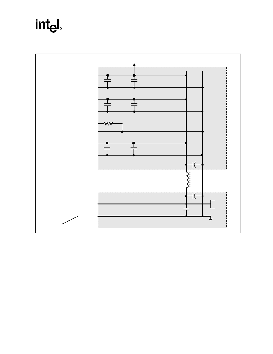
Advanced 10/100 Unmanaged Repeater -- LXT9883/9863
Datasheet
35
Document #: 249115
Revision #: 003
Rev. Date: 08/07/01
4.2.6
MII Terminations
The LXT98x3 MIIs have high output impedance (250-350
). To minimize reflections, serial
termination resistors are recommended on all MII signals, especially with designs with long traces
(>3 inches). Place the resistor as close to the device as possible. Use a software trace termination
package to select an optimal resistance value for the specific trace. Proper value = nominal trace
impedance minus 13
. If a software package cannot be used and nominal trace impedance is not
known, use 55
.
Figure 10. Power and Ground Connections
RBIAS
VCC
GND
GND
VCC
GND
.01
µ
F
22.1k
1%
GND
VCC
0.1
µ
F
+
Ferrite
Beads
10
µ
F
+3.3V
LXT9883
VCCT
GND
10
µ
F
.01
µ
F
.1
µ
F
.1
µ
F
Digital Supply Plane
Analog Supply Plane
.01
µ
F
.1
µ
F
To Output Magnetics Centertap
LXT9883/9863 -- Advanced 10/100 Unmanaged Repeater
36
Datasheet
Document #: 249115
Revision #: 003
Rev. Date: 08/07/01
4.2.7
Twisted-Pair Interface
The LXT98x3 transmitter uses standard 1:1 magnetics for both receive and transmit. Nonetheless,
system designers should take precautions to minimize parasitic shunt capacitance and meet return
loss specifications. These steps include:
∑
Place magnetics as close as possible to the LXT98x3.
∑
Keep transmit pair traces short.
∑
Do not route transmit pair adjacent to a ground plane. Eliminate planes under the transmit
traces completely. Otherwise, keep planes 3-4 layers away.
∑
Improve EMI performance by filtering the output center tap supply. A single ferrite bead may
be used in the center tap supply to all ports. All ports draw a combined total of > 1000 mA, so
the bead should be rated at > 1500 mA.
∑
Place the 270pF 5% capacitors at TPIP and TPIN to improve the signal-to-noise immunity at
the receiver.
In addition, follow all the standard guidelines for a twisted-pair interface:
∑
Route the signal pairs differentially, close together. Allow nothing to come between them.
∑
Keep distances as short as possible; both traces should have the same length.
∑
Avoid vias and layer changes.
∑
Keep the transmit and receive pairs apart to avoid cross-talk.
∑
To provide maximum isolation, place entire receive termination network on one side and
transmit on the other side of the PCB.
∑
Bypass common-mode noise to ground on the in-board side of the magnetics using 0.01
µ
F
capacitors.
∑
Keep termination circuits grouped closely together and on the same side of the board.
∑
Always put termination circuits close to the source end of any circuit.
4.2.7.1
Magnetics Information
The LXT98x3 requires a 1:1 ratio for the receive transformers and a 1:1 ratio for the transmit
transformers. The transformer isolation voltage should be rated at 2kV to protect the circuitry from
static voltages across the connectors and cables. Refer to
Table 17
for magnetics specifications.
Table 17. LXT98x3 Magnetics Specifications
Parameter
Min
Nom
Max
Units
Test Condition
Rx turns ratio
≠
1 : 1
≠
≠
Tx turns ratio
≠
1 : 1
≠
≠
Insertion loss
0.0
≠
1.1
dB
80 MHz
Primary inductance
350
≠
≠
µ
H
Transformer isolation
≠
2
≠
kV
Differential to common mode rejection
-40
≠
≠
dB
.1 to 60 MHz
Advanced 10/100 Unmanaged Repeater -- LXT9883/9863
Datasheet
37
Document #: 249115
Revision #: 003
Rev. Date: 08/07/01
4.2.8
Clock
A stable, external 25MHz reference clock source (TTL) is required to the CLK25 pin. The
reference clock is used to generate transmit signals and recover receive signals. A crystal-based
clock is recommended over a derived clock (i.e., PLL-based) to minimize transmit jitter. Refer to
Table 18
for a list of recommended oscillators and to
Table 21 on page 44
for clock timing
requirements.
-35
≠
≠
dB
60 to 100 MHz
Return Loss - standard
-16
≠
≠
dB
30 MHz
-10
≠
≠
dB
80 MHz
Table 17. LXT98x3 Magnetics Specifications
Parameter
Min
Nom
Max
Units
Test Condition
Table 18. Oscillator Manufacturers
Manufacturer
Part Number
Frequency
CTS
MXO45 / 45LV
25 MHz
Epson America
SG-636 Series
25 MHz
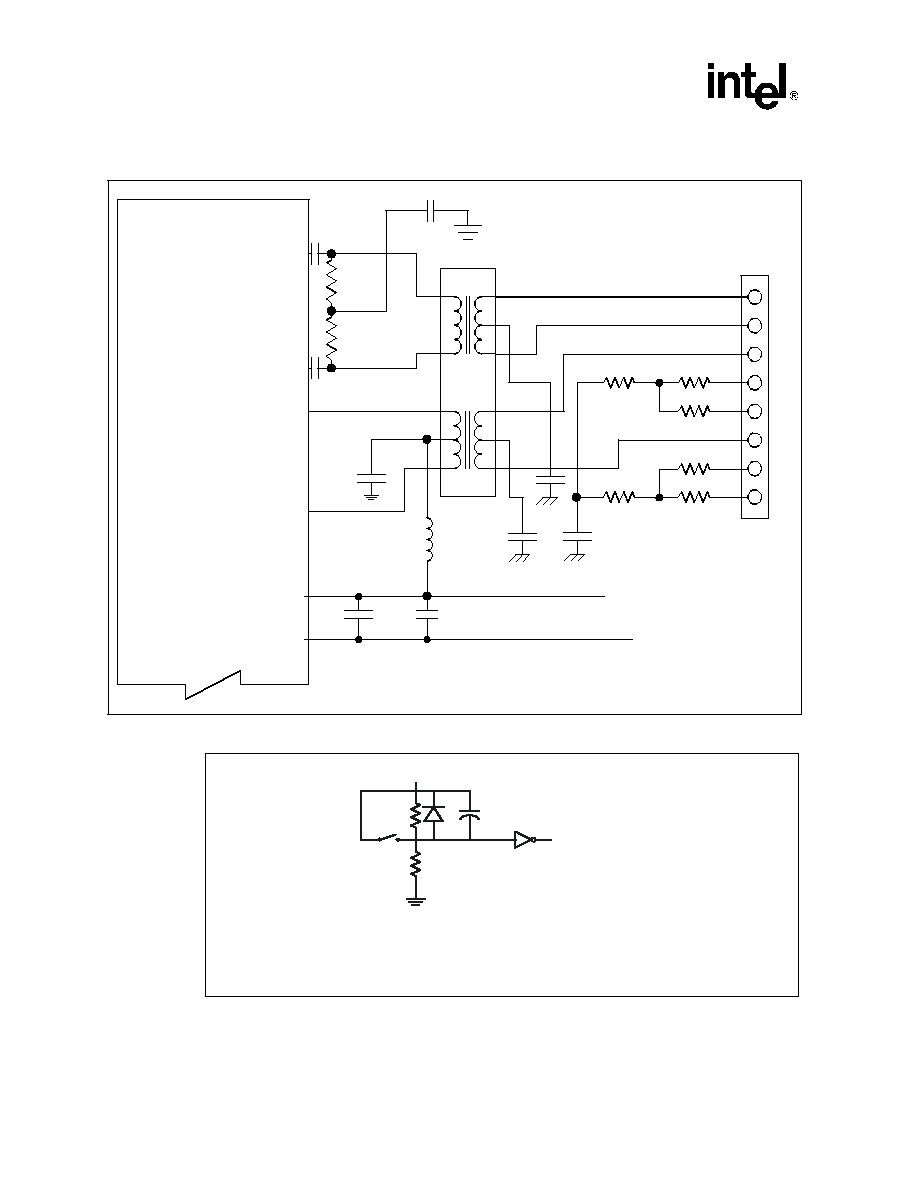
LXT9883/9863 -- Advanced 10/100 Unmanaged Repeater
38
Datasheet
Document #: 249115
Revision #: 003
Rev. Date: 08/07/01
Figure 11. Typical Twisted-Pair Port Interface and Power Supply Filtering
Figure 12. Typical Reset Circuit
TPFIP
TPIN
RJ45
TPOP
TPON
VCCT
GND
0.1
µ
F
.01
µ
F
50
1%
T
o
T
w
i
s
te
d
-
P
a
i
r
N
e
tw
o
r
k
3
6
1
2
1:1
1:1
LXT98x3
50
50
50
50
50
50
4
5
8
7
50
1%
0.01
µ
F
5%
270 pF 5%
270 pF 5%
0.001
µ
F
2kV
0.001
µ
F
2kV
0.001
µ
F
2kV
TPIP
.01
µ
F
VCC
C
R1
R2
'14
D
NOTE: t(CR1 > Power Supply Ramp Up Time. R2 discharges C when
supply goes away. The `14 is needed for multiple LXT98x3
devices.
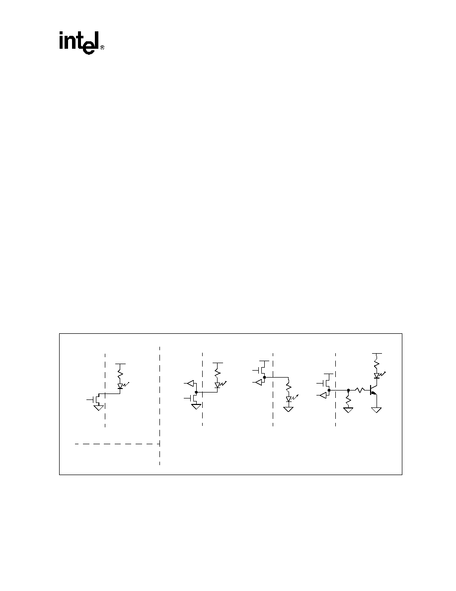
Advanced 10/100 Unmanaged Repeater -- LXT9883/9863
Datasheet
39
Document #: 249115
Revision #: 003
Rev. Date: 08/07/01
4.2.9
LED Circuits
4.2.9.1
Direct Drive LEDs
Each Direct Drive LED has a corresponding open-drain pin. The LEDs are connected, via a current
limiting resistor, to a positive voltage rail. The LEDs are turned on when the output pin drives Low.
The open-drain LED pins are 5V tolerant, allowing use of either a 3.3V or 5V rail. A 5V rail eases
LED component selection by allowing more common, high forward voltage LEDs to be used.
Refer to
Figure 13
for a circuit illustration.
4.2.9.2
LED Pins Multiplexed with Configuration Inputs
Some static configuration inputs are multiplexed with LED pins to reduce the LXT98x3 pin count.
These LED pins are configured by current sinking (open- drain output) and sourcing (open-source
output). If the LED pin sinks the LED current, the configuration value is `1'. If LED pin sources
the current, the configuration value is a `0'. The LXT98x3 detects the configuration value
following reset and then selects the appropriate output drive circuit (open drain or source). If the
LED function of a multiplexed configuration pin is not used, tie the pin to Ground or Vcc via a
100≠500k
resistor to set the configuration value. Multiple LED configuration pins can be tied off
with a single resistor to set them all to the same value. Refer to
Figure 13
for a circuit illustration.
For configuration values of `1', a 3.3V or a 5V rail can be used to drive the LEDs (to ease LED
selection as with Direct Drive LEDs).
For configuration values of `0', external buffering is used when 5V LED driving is desired. (This
buffering could be as simple as a single transistor.) As an alternative, use the copies of the
multiplexed LED data found on the LED serial interface. 5V LED driving is achieved. Also, if a
5V tolerant serial-to-parallel device is used for the LED serial interface, 5V LED driving is
achieved (see
"Serial LEDs" on page 40.
).
Figure 13. LED Circuits - Direct Drive &
Multiplexed Configuration Inputs
Inside
IC
Outside
IC
Direct Drive
R
V
LED
Inside
IC
Outside
IC
Configuration
= `1'
Inside
IC
Outside
IC
Configuration
= `0'
R
V
LED
R
V
LED
= 3.3 to 5 Volts +/- 5%
Multiplexed
Multiplexed
V
cc
= 3.3 Volts +/- 5%
Inside
IC
Outside
IC
Configuration
= `0'
V
cc
Multiplexed
with Transistor Buffer
R
V
LED
100k
Rb
V
cc
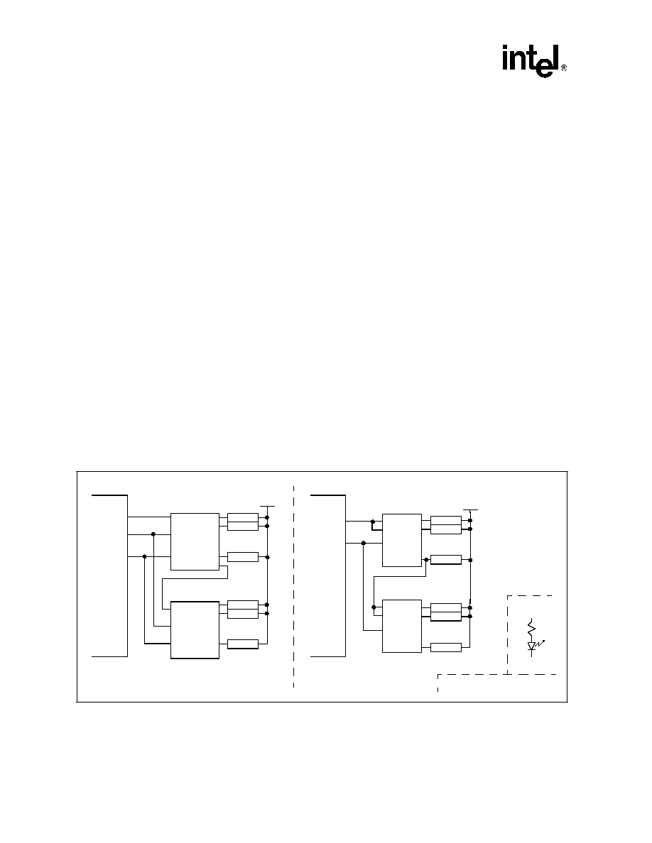
LXT9883/9863 -- Advanced 10/100 Unmanaged Repeater
40
Datasheet
Document #: 249115
Revision #: 003
Rev. Date: 08/07/01
4.2.9.3
Serial LEDs
The LXT98x3 provides a serial interface to support additional LED options. Standard shift
registers, either 74X595s (8-bit Serial-to-Parallel with Output Registers) or 74X164s (8-bit S/P
without registers) can be used to drive these additional LEDs. Collision10/100 and Activity10/100
status indications are provided on multiplexed configuration pins and duplicated on the serial port.
The LED serial interface consists of three outputs: clock (LEDCLK), parallel latch clock
(LEDLAT), and output data (LEDDAT). The parallel latch clock is used only with the 74X595
implementation. Refer to
Figure 14
for an illustration of the LED serial interface circuit.
Potentially, 30 LEDs can be driven by the LED serial interface via 4 S/P devices. The S/P serial
output is connected to the serial input of the first serial input device. To expand the chain, connect
the last serial output to serial input of next serial interface device.
Serial LED data is output in the anticipated priority order, from least likely to most likely to be
used:
∑
Unused `595/`164 parallel outputs
∑
MII Ports - LED1, 2, 3
∑
Miscellaneous LEDs (Repeat of Collision10/100, Repeat of Activity10/100, Global Fault,
RPS Fault)
∑
ACTGLED10
∑
ACTGLED100
This allows the user to leave off devices in the serial-to-parallel chain if the LEDs associated with
that condition aren't desired. Refer to
Figure 6 on page 23
which illustrates the LED serial interface
port signalling and
Table 8 on page 23
which documents the Serial LED Stream.
.
Figure 14. Serial LED Circuit
SER
RCLK
SRCLK
Qa
Qb
.
.
.
Qh
Qh`
LED cct.
LED cct.
LED cct.
R
V
LED
LED cct.
V
LED
side
.
.
.
V
LED
= 3.3 to 5 Volts +/- 5%
74X595
.
.
.
LED cct.
LED cct.
LED cct.
.
.
.
Up to 2 more
`595s/8xLEDs
LEDDAT
LEDLAT
LEDCLK
.
.
.
Up to 2 more
`164s/8xLEDs
LED cct.
LED cct.
LED cct.
V
LED
.
.
.
LED cct.
LED cct.
LED cct.
.
.
.
LEDDAT
LEDCLK
Qa
Qb
.
.
.
Qh
A
B
CLK
74X164
Qa
Qb
.
.
.
Qh
A
B
CLK
74X164
ACTG
L
E
D
1
0
0
AC
T
G
L
E
D
1
0
AC
T
G
L
E
D1
0
0
ACTG
L
E
D1
0
SER
RCLK
SRCLK
Qa
Qb
.
.
.
Qh
Qh`
74X595
LXT98x3
LXT98x3

Advanced 10/100 Unmanaged Repeater -- LXT9883/9863
Datasheet
41
Document #: 249115
Revision #: 003
Rev. Date: 08/07/01
4.3
Inter-Repeater Backplane Compatibility
The Inter-repeater Backplane (IRB) comprises two parts:
∑
Local--the backplane between cascaded devices on the same board.
∑
Stack--the backplane between multiple boards.
Each of these backplanes consists of both analog and digital signals.
4.3.1
Local Backplane--3.3V Only
The LXT98x3 local backplane operates at 3.3V only. LXT98x and LXT91x devices operate at 5V.
LXT98x3 devices are, therefore, not cascadable with LXT98x and LXT91x devices.
Note:
Do not mix LXT98x3 with either LXT98x or LXT91x devices on the local backplanes.
4.3.2
Stack Backplane--3.3V or 5V
The LXT98x3 stack backplanes can be configured to be either 3.3V or 5V. COMP_SEL (Pin 39), a
special input pin, selects between the two voltage modes, depending on whether 3.3V or 5V is
applied.
4.3.2.1
3.3V-Only Stacks
Apply 3.3V to COMP_SEL, IR100CFSBP, IR10CFSBP, and IR10COLBP for LXT98x3 backplane
operation
4.3.2.2
For 5V Backwards Stackability
Apply 5V to COMP_SEL, IR100CFSBP, IR10CFSBP, and IR10COLBP for LXT98x and LXT91x
backplane operation.
Note:
With either mode (3.3V or 5V), COMP_SEL draws less than 3 mA.
1. The external pull-up resistor values remain the same, regardless of 3.3V or 5V backplane
operation.
2. The recommended digital signal external buffer has been changed to 74LVT245 for the
LXT98x3.
4.3.2.3
3.3V and 5.0V Stacking Boards Cannot Be Mixed
4.3.2.3.1
3.3V Operation
Boards designed for 3.3V backplane operation should only be stacked with other 3.3V boards.
Existing LXT98x or LXT91x based designs cannot operate in 3.3V.
4.3.2.3.2
Incompatible Stacking Configurations
The following stacking configurations are incompatible:
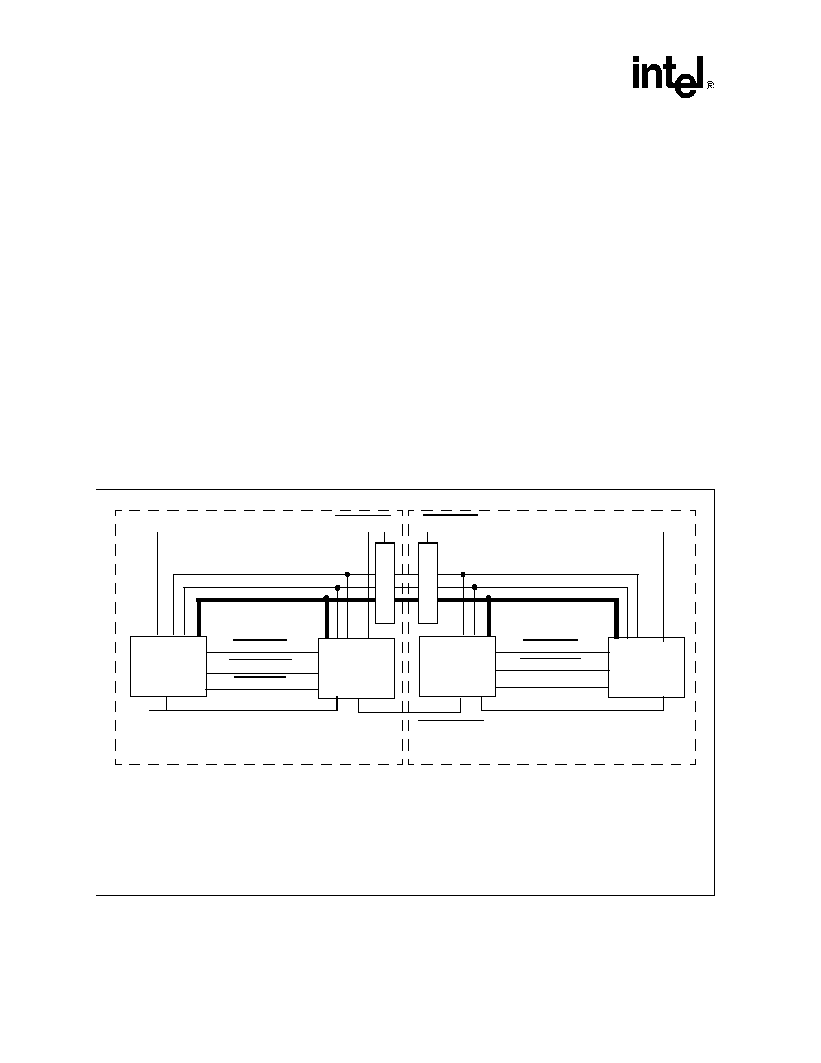
LXT9883/9863 -- Advanced 10/100 Unmanaged Repeater
42
Datasheet
Document #: 249115
Revision #: 003
Rev. Date: 08/07/01
∑
A LXT98x3-based board configured for 3.3V backplane operation and LXT98x or LXT91x
based boards (5V only).
∑
A LXT98x3-based board configured for 3.3V backplane operation and a LXT98x3-based
board configured for 5V backplane operation.
Note:
Stacking boards designed for 3.3V backplane operation with boards designed for 5V backplane
operation causes network errors.
4.3.2.3.3
5V Operation
Boards designed for 5V backplane operation should only be stacked with other 5V boards:
∑
LXT98x or LXT91x-based designs.
∑
LXT98x3 designs configured for 5V backplane operation.
The configuration input must be connected to 5V for compatibility with LXT98x or LXT91x-based
designs. The 5V can be supplied from the stacking cable, or a 5V source must exist within the
board itself.
Caution:
Stacking boards designed for 5V backplane operation with boards designed for 3.3V backplane
operation causes network errors.
Figure 15. 100M Backplane Connection between LXT98x and LXT98x3
IR100DAT(4:0)
IR100DV
IR100CLK
IR100CFS
IR100DAT(4:0)
IR100DV
IR100CLK
IR100CFSBP
HUB #1
HUB #2
98x3
Bu
f
f
e
r
Bu
f
f
e
r
IR100DEN
IR100DEN
IR100SNGL
IR100COL
IR100CFS
IR100SNGL
IR100COL
(000)
(00)
98x3
98x
1. The LXT98x and LXT9883 devices can share the same Inter-Repeater Backplane so long as the proper backplane
buffers are used. Configuration is set to 5V.
2. For LXT98x, LXT91x: The buffer should be the 74ABT245.
For LXT9883: In the 5V tolerant backplane, the buffer can be either 74ABT245 or 74LVT245
3. Layout follows the same pattern for 10M operation.
98x
5V
5V
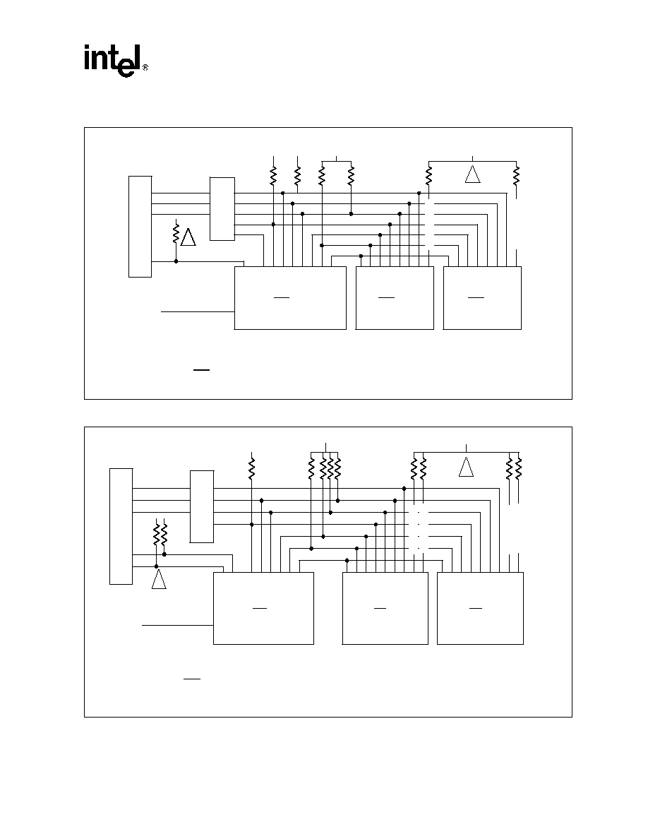
Advanced 10/100 Unmanaged Repeater -- LXT9883/9863
Datasheet
43
Document #: 249115
Revision #: 003
Rev. Date: 08/07/01
Figure 16. Typical 100 Mbps IRB Implementation
Figure 17. Typical 10 Mbps IRB Implementation
LXT98x3
FPS = 1
LXT98x3
FPS = 1
215
1%
300
IR100DV\
IR100DAT <4:0>
IR100CFS\
IR100COL\
IR100SNGL
'245
IR100DATBP
IR100DVBP\
DIR
ENA
IR100CLKBP
A
B
LXT98x3
FPS = 0
IR100CFSBP\
IR100DEN\
ISOLATE
91
1%*
+3.3V
330
IR100CLK
IR100DEN\
IR100DV\
IR100DAT
Stack or
Segment
Connector
IR
100C
F
SBP\
+3.3V
91
91
2
1
1
COMP_SEL
+3.3V
+3.3V
IR
100C
F
SBP\
1. In stacked configurations, all devices with FPS/ = 0 are tied together at IR100CFSBP. The entire stack must
be pulled up by only one resistor per signal. Pull-up resistor is installed on one board only. (Board selection
is application specific.)
2. All devices with FPS
0 require individual pull-up resistors at IR100CFSBP.
3. Pull-up voltage should be the same as COMP_SEL.
LXT9883
FPS 1
LXT9883
FPS 1
+3.3V
215
1%
330
IR10ENA\
IR10DAT
IR10CFS\
IR10COL\
HOLDCOL
IR10CLK
'245
IR10DATBP
IR10ENABP\
DIR
ENA
IR10CLKBP
A
B
LXT9883
FPS 0
IR10COLBP\
IR10CFSBP\
IR10DEN\
330
1%
330
1%
+3.3V
330
IR10DEN\
IR10CLK
IR10ENA\
IR10DAT
I
R
10CO
L
BP\
I
R
10CFSBP\
I
R
10CO
L
BP\
I
R
10CFSBP\
+3.3V
330
330
330
330
Stack or
Segment
Connector
2
1
COMP_SEL
1. In stacked configurations, all devices with FPS/ = 0 are tied together at IR100CFSBP. The entire stack must be
pulled up by only one resistor per signal. Pull-up resistor is installed on one board only. (Board selection is
application specific.)
2. All devices with FPS
0 require individual pull-up resistors at IR100CFSBP.
3. Pull-up voltage should be the same as COMP_SEL.
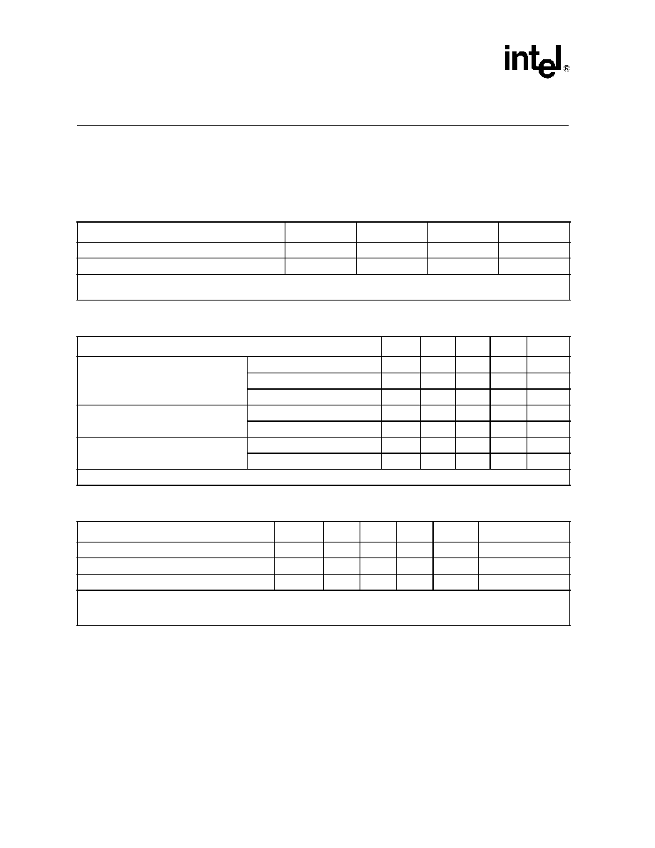
LXT9883/9863 -- Advanced 10/100 Unmanaged Repeater
44
Datasheet
Document #: 249115
Revision #: 003
Rev. Date: 08/07/01
5.0
Test Specifications
Note:
Table 19
through
Table 34
and
Figure 18
through
Figure 25
represent the target specifications of
the LXT98x3 and are subject to change. Final values will be guaranteed by test except, where
noted, by design. The minimum and maximum values listed in
Table 21
through
Table 34
will be
guaranteed over the recommended operating conditions specified in
Table 20
.
Table 19. Absolute Maximum Ratings
Parameter
Symbol
Min
Max
Units
Supply voltage
V
CC
-0.3
4.0
V
Storage temperature
T
ST
-65
+150
∫C
Caution: Exceeding these values may cause permanent damage. Functional operation under these conditions is not implied.
Exposure to maximum rating conditions for extended periods may affect device reliability.
Table 20. Operating Conditions
Parameter
Sym
Min
Typ
1
Max
Units
Recommended supply voltage
V
CC
3.15
3.3
3.45
V
V
CCR
3.15
3.3
3.45
V
V
CCT
3.15
3.3
3.45
V
Recommended operating temperature
Ambient
T
OPA
0
≠
70
∞C
Case
T
OPC
0
≠
115
∞C
Power consumption
8 ports active
P
C
≠
≠
3.03
W
6 ports active
P
C
≠
≠
2.50
W
1. Typical values are at 25∞ C and are for design aid only; they are not guaranteed and not subject to production testing.
Table 21. Input System Clock
1
Requirements
Parameter
2
Symbol
Min
Typ
3
Max
Units
Test Conditions
Frequency
≠
≠
25
≠
MHz
≠
Frequency Tolerance
≠
≠
≠
±100
PPM
≠
Duty Cycle
≠
40
≠
60
%
≠
1. The system clock is CLK25 (Pin 54).
2. These requirements apply to the external clock supplied to the LXT98x3, not to LXT98x3 test specifications.
3. Typical values are at 25 ∞C and are for design aid only; not guaranteed and not subject to production testing.
Advanced 10/100 Unmanaged Repeater -- LXT9883/9863
Datasheet
45
Document #: 249115
Revision #: 003
Rev. Date: 08/07/01
Table 22. I/O Electrical Characteristics
Parameter
Sym
Min
Typ
1
Max
Units
Test Conditions
Input Low voltage
V
IL
≠
≠
0.8
V
TTL inputs
≠
≠
30
% V
CC
CMOS inputs
2
≠
≠
1.0
Schmitt triggers
3
Input High voltage
V
IH
2.0
≠
≠
V
TTL inputs
70
≠
≠
% V
CC
CMOS inputs
2
V
CC
- 1.0
≠
≠
V
Schmitt triggers
3
Hysteresis voltage
≠
1.0
≠
≠
V
Schmitt triggers
3
Output Low voltage
V
OL
≠
≠
0.4
V
I
OL
= 1.6 mA
Output Low voltage (LED)
V
OLL
≠
≠
1.0
V
I
OLL
= 10 mA
Output High voltage
V
OH
2.2
≠
≠
V
I
OH
= 40
µ
A
Input Low current
I
IL
-100
≠
≠
µ
A
≠
Input High current
I
IH
≠
≠
100
µ
A
≠
Output rise / fall time
T
RF
≠
3
10
ns
C
L
= 15 pF
1. Typical values are at 25 ∞C and are for design aid only; not guaranteed and not subject to production testing.
2. Does not apply to IRB pins. Refer to
Table 23
and
Table 24
for IRB I/O characteristics.
3. Applies to RESET, CLK25, IR100SNGL, IR100COL, IR100DV, IR100DATn, IR100CLK, and IR10CLK pins.
Table 23. 100 Mbps IRB Electrical Characteristics
Parameter
Symbol
Min
Typ
1
Max
Units
Test Conditions
Output Low voltage
V
OL
≠
.3
.7
V
R
L
= 330
Output rise or fall time
T
RF
≠
4
10
ns
C
L
=
1
5 pF
Input High voltage
V
IH
V
CC
- 2.0
≠
≠
V
CMOS inputs
V
CC
- 1.0
≠
≠
V
IR100CLK (Schmitt trigger)
Input Low voltage
V
IL
≠
≠
2.0
V
CMOS inputs
≠
≠
1.0
IR100CLK (Schmitt trigger)
Hysteresis voltage
≠
1.0
≠
≠
V
IR100CLK (Schmitt trigger)
3.3V Operation
IR100CFS
current
single drive
≠
≠
6.8
≠
mA
R
L
= 215
collision
≠
≠
13.5
≠
mA
R
L
= 215
IR100CFSBP
current
single drive
≠
≠
16.1
≠
mA
R
L
= 91
2
collision
≠
≠
31.8
≠
mA
R
L
= 91
2
IR100CFS/BP
voltage
single drive
≠
≠
1.83
≠
V
≠
collision
≠
≠
0.4
≠
V
≠
1. Typical values are at 25∞ C and are for design aid only; they are not guaranteed and not subject to production testing.
2. 91
resistors provide greater noise immunity. Systems using 91
resistors
are backwards stackable with systems using
100
resistors.

LXT9883/9863 -- Advanced 10/100 Unmanaged Repeater
46
Datasheet
Document #: 249115
Revision #: 003
Rev. Date: 08/07/01
5.0V Operation
IR100CFS
current
single drive
≠
≠
N/A
≠
mA
R
L
= 215
collision
≠
≠
N/A
≠
mA
R
L
= 215
IR100CFSBP
current
single drive
≠
≠
24.2
≠
mA
R
L
= 91
2
collision
≠
≠
42
≠
mA
R
L
= 91
2
IR100CFS/BP
voltage
single drive
≠
≠
2.8
≠
V
≠
collision
≠
≠
0.6
≠
V
≠
Table 24. 10 Mbps IRB Electrical Characteristics
Parameter
Symbol
Min
Typ
1
Max
Units
Test Conditions
Output Low voltage
V
OL
0
.1
.4
V
R
L
= 330
Output rise or fall time
T
RF
≠
4
10
ns
C
L
= 15 pF
Input High voltage
V
IH
V
CC
- 2.0
≠
≠
V
CMOS inputs
V
CC
- 2.0
≠
≠
V
IR10CLK (Schmitt trigger)
Input Low voltage
V
IL
≠
≠
2.0
V
CMOS inputs
≠
≠
1.0
V
IR10CLK (Schmitt trigger)
Hysteresis voltage
≠
0.5
≠
≠
V
IR10CLK (Schmitt trigger)
3.3V Operation
IR10CFS current
single drive
≠
≠
6.8
≠
mA
R
L
= 215
collision
≠
≠
13.5
≠
mA
R
L
= 215
IR10CFSBP current
single drive
≠
≠
4.5
≠
mA
R
L
= 330
collision
≠
≠
8.8
≠
mA
R
L
= 330
IR10CFS/BP voltage
single drive
≠
1.3
1.83
2.4
V
≠
collision
≠
0.2
0.4
0.6
V
≠
5.0V Operation
IR10CFS current
single drive
≠
≠
N/A
≠
mA
R
L
= 215
collision
≠
≠
N/A
≠
mA
R
L
= 215
IR10CFSBP current
single drive
≠
≠
7.0
≠
mA
R
L
= 330
collision
≠
≠
13.5
≠
mA
R
L
= 330
IR10CFS/BP voltage
single drive
≠
1.9
2.8
3.2
V
≠
collision
≠
0.4
0.6
0.8
V
≠
1. Typical values are at 25∞ C and are for design aid only; they are not guaranteed and not subject to production testing.
Table 23. 100 Mbps IRB Electrical Characteristics (Continued)
Parameter
Symbol
Min
Typ
1
Max
Units
Test Conditions
1. Typical values are at 25∞ C and are for design aid only; they are not guaranteed and not subject to production testing.
2. 91
resistors provide greater noise immunity. Systems using 91
resistors
are backwards stackable with systems using
100
resistors.
Advanced 10/100 Unmanaged Repeater -- LXT9883/9863
Datasheet
47
Document #: 249115
Revision #: 003
Rev. Date: 08/07/01
Table 25. 100BASE-TX Transceiver Electrical Characteristics
Parameter
Symbol
Min
Typ
1
Max
Units
Test Conditions
Peak differential output voltage
(single ended)
V
P
0.95
1.0
1.05
V
Note 2
Signal amplitude symmetry
≠
98
≠
102
%
Note 2
Signal rise/fall time
Trf
3.0
≠
5.0
ns
Note 2
Rise/fall time symmetry
Trfs
≠
≠
0.5
ns
Note 2
Duty cycle distortion
≠
≠
≠
+/- 0.5
ns
Offset from 8 ns pulse width at 50%
of pulse peak,
Overshoot
Vo
≠
≠
5
%
≠
1. Typical values are at 25 ∞C and are for design aid only; not guaranteed and not subject to production testing.
2. Measured at line side of transformer, line replaced by 100
(±1%) resistor.
Table 26. 10BASE-T Transceiver Electrical Characteristics
Parameter
Symbol
Min
Typ
1
Max
Units
Test Conditions
Transmitter
Peak differential output voltage
V
P
2.2
2.5
2.8
V
Measured at line side of
transformer, line replaced by 100
(± .1%) resistor
Transmit timing jitter addition
2
≠
8
≠
24
ms
0 line length for internal MAU
Transmit timing jitter added by the
MAU and PLS sections
2, 3
≠
0
≠
11
ns
After line model specified by IEEE
802.3 for 10BASE-T internal MAU
Receiver
Receive input impedance
Z
IN
≠
20
≠
k
Between TPIP/TPIN
Differential Squelch Threshold
V
DS
≠
390
≠
mV
5 MHz square wave input,
750 mVpp
1. Typical values are at 25 ∞C and are for design aid only; not guaranteed and not subject to production testing.
2. Parameter is guaranteed by design; not subject to production testing.
3. IEEE 802.3 specifies maximum jitter additions at 1.5 ns for the AUI cable, 0.5 ns from the encoder, and 3.5 ns from the MAU.
LXT9883/9863 -- Advanced 10/100 Unmanaged Repeater
48
Datasheet
Document #: 249115
Revision #: 003
Rev. Date: 08/07/01
Figure 18. 100 Mbps TP Port-to-Port Delay Timing
Table 27. 100 Mbps TP Port-to-Port Delay Timing Parameters
Parameter
Symbol
Min
Typ
1
Max
Units
2
Test Conditions
TPIP/N to TPOP/N, start of transmission
t
1A
≠
≠
46
BT
≠
TPIP/N to TPOP/N, end of transmission
t
1B
≠
≠
46
BT
≠
TPIP/N collision to TPOP/N, start of jam
t
1C
≠
≠
46
BT
≠
TPIP/N idle to TPOP/N, end of jam
t
1D
≠
≠
46
BT
≠
1. Typical values are at 25 ∞C and are for design aid only; not guaranteed and not subject to production testing.
2. Bit Time (BT) is the duration of one bit as transferred to/from the MAC and is the reciprocal of bit rate. BT for
100BASE-T = 10
-8
s or 10ns.
TP Input #2
t
1C
P Input #1
TP Output
Jam
t
1D
t
1A
TP Input
TP Output
t
1B
Normal Propagation
Collision Jamming
Advanced 10/100 Unmanaged Repeater -- LXT9883/9863
Datasheet
49
Document #: 249115
Revision #: 003
Rev. Date: 08/07/01
Figure 19. 100BASE-TX MII-to-TP Port Timing
Table 28. 100BASE-TX MII-to-TP Port Timing Parameters
Parameter
Sym
Min
Typ
1
Max
Units
2
Test Condition
TXD, TX_EN, TX_ER Setup to TX_CLK High
t
2A
10
≠
≠
ns
≠
TXD, TX_EN, TX_ER Hold from TX_CLK High
t
2B
5
≠
≠
ns
≠
TX_EN sampled to CRS asserted
t
2C
0
≠
4
BT
≠
TX_EN sampled to CRS de-asserted
t
2D
0
≠
16
BT
≠
TX_EN sampled to TPOP/N active (Tx latency)
t
2E
≠
≠
46
BT
≠
1. Typical values are at 25 ∞C and are for design aid only; not guaranteed and not subject to production testing.
2. Bit Time (BT) is the duration of one bit as transferred to/from the MAC and is the reciprocal of bit rate. BT for
100BASE-T = 10
-8
s or 10ns.
TX_CLK
TXD,
TX_EN,
TX_ER
CRS
TPOP/N
t
2A
t
2B
t
2C
t
2D
t
2E
LXT9883/9863 -- Advanced 10/100 Unmanaged Repeater
50
Datasheet
Document #: 249115
Revision #: 003
Rev. Date: 08/07/01
Figure 20. 100BASE-TX TP-to-MII Timing
Table 29. 100BASE-TX TP-to-MII Timing Parameters
Parameter
Sym
Min
Typ
1
Max
Units
2
Test Conditions
TPIP/N in to CRS asserted
t
3A
≠
≠
46
BT
≠
TPIP/N quiet to CRS de-asserted
t
3B
≠
≠
46
BT
≠
CRS asserted to RXD, RX_DV,
RX_ER
t
3C
1
≠
4
BT
≠
CRS de-asserted to RXD, RX_DV,
RX_ER de-asserted
t
3D
≠
≠
3
BT
≠
RX_CLK falling edge to RXD,
RX_DV, RX_ER valid
t
3E
≠
≠
10
ns
≠
TPIP/N in to COL asserted
t
3F
≠
≠
46
BT
≠
TPIP/N quiet to COL de-asserted
t
3G
≠
≠
46
BT
≠
1. Typical values are at 25 ∞C and are for design aid only; not guaranteed and not subject to production testing.
2. Bit Time (BT) is the duration of one bit as transferred to/from the MAC and is the reciprocal of bit rate. BT for
100BASE-T = 10
-8
s or 10ns.
RX_CLK
RXD,
RX_DV,
RX_ER
CRS
TPIP/N
COL
t
3A
t
3B
t
3C
t
3D
t
3F
t
3G
t
3E
Advanced 10/100 Unmanaged Repeater -- LXT9883/9863
Datasheet
51
Document #: 249115
Revision #: 003
Rev. Date: 08/07/01
Figure 21. 10BASE-T MII-to-TP Timing
Table 30. 10BASE-T MII-to-TP Timing Parameters
Parameter
Sym
Min
Typ
1
Max
Units
2
Test Conditions
TXD, TX_EN, TX_ER Setup to TX_CLK High
t
10A
10
≠
≠
ns
≠
TXD, TX_EN, TX_ER Hold from TX_CLK High
t
10B
5
≠
≠
ns
≠
TX_EN sampled to CRS asserted
t
10C
0
.9
2
BT
≠
1. Typical values are at 25 ∞C and are for design aid only; not guaranteed and not subject to production testing.
2. Bit Time (BT) is the duration of one bit as transferred to/from the MAC and is the reciprocal of bit rate. BT for
10BASE-T = 10
-7
s or 100ns.
TX_CLK
TXD,
TX_EN,
TX_ER
CRS
t
10A
t
10B
t
10C
LXT9883/9863 -- Advanced 10/100 Unmanaged Repeater
52
Datasheet
Document #: 249115
Revision #: 003
Rev. Date: 08/07/01
Figure 22. 10BASE-T TP-to-MII Port Timing
Table 31. 10BASE-T TP-to-MII Port Timing Parameters
Parameter
Sym
Min
Typ
1
Max
Units
2
Test Conditions
TPIP/N in to CRS asserted
t
11A
5
6.6
8
BT
≠
CRS asserted to RXD, RX_DV,
RX_ER
t
11B
70
76
84
BT
≠
RX_CLK falling edge to RXD,
RX_DV, RX_ER valid
t
11C
≠
≠
10
ns
≠
TPIP/N in to COL asserted
t
11D
6
7.4
9
BT
≠
1. Typical values are at 25 ∞C and are for design aid only; not guaranteed and not subject to production testing.
2. Bit Time (BT) is the duration of one bit as transferred to/from the MAC and is the reciprocal of bit rate. BT for
10BASE-T = 10
-7
s or 100ns.
RX_CLK
RXD,
RX_DV,
RX_ER
CRS
TPIP/N
COL
t
11A
t
11B
t
11C
t
11D
Advanced 10/100 Unmanaged Repeater -- LXT9883/9863
Datasheet
53
Document #: 249115
Revision #: 003
Rev. Date: 08/07/01
Figure 23. 100 Mbps TP-to-IRB Timing
Table 32. 100 Mbps TP-to-IRB Timing Parameters
1
Parameter
Symbol
Min
Typ
2
Max
Units
3
Test Conditions
TPIP/N to IR100DV Low
t
12A
18
24
30
BT
≠
IR100DAT to IR100CLK setup time.
t
12B
≠
10
≠
ns
≠
IR100DAT to IR100CLK hold time.
t
12C
≠
0
≠
ns
≠
1. This table contains propagation delays from the TP ports to the IRB for normal repeater operation. All values in this table are
output timings.
2. Typical figures are at 25 C and are for design aid only; not guaranteed and not subject to production testing.
3. Bit Time (BT) is the duration of one bit as transferred to/from the MAC and is the reciprocal of bit rate. BT for
100BASE-T = 10
-8
s or 10ns.
TPIP/N
IR100DV
IR100CFS
1R100COL
IR100DAT<4:0>
t
12A
t
12B
IR100CLK
t
12C
LXT9883/9863 -- Advanced 10/100 Unmanaged Repeater
54
Datasheet
Document #: 249115
Revision #: 003
Rev. Date: 08/07/01
Figure 24. 10 Mbps TP-to-IRB Timing
Table 33. 10 Mbps TP-to-IRB Timing Parameters
1
Parameter
2
Symbol
Min
Typ
3
Max
Units
4
Test Conditions
TPIP/N to IR10ENA Low
t
13A
3
5.1
7
BT
≠
IR10CLK rising edge to
IR10DAT rising edge.
t
13B
25
-
55
ns
330
pull-up, 150pF load on IR10DAT.
1 k
pull-up, 150pF load on IRCLK.
IR10CLK rising edge to
IR10DAT falling edge.
t
13C
5
-
25
ns
1. This table contains propagation delays from the TP ports to the IRB for normal repeater operation. All values in this table are
output timings.
2. There is a delay of approximately 13 to 16 bit times between the assertion of IR10ENA and the assertion of IR10CLK and
IR10DAT. This delay does not affect repeater operation because downstream devices begin generating preamble as soon as
IR10ENA is asserted.
3. Typical values are at 25 ∞C and are for design aid only; not guaranteed and not subject to production testing.
4. Bit Time (BT) is the duration of one bit as transferred to/from the MAC and is the reciprocal of bit rate. BT for
10BASE-T = 10
-7
s or 100ns.
TPIP/N
IR10ENA
IR10DAT
t
13A
t
13B
IR10CLK
t
13C

Advanced 10/100 Unmanaged Repeater -- LXT9883/9863
Datasheet
55
Document #: 249115
Revision #: 003
Rev. Date: 08/07/01
Figure 25. 10 Mbps IRB-to-TP Port Timing
Table 34. 10 Mbps IRB-to TP Port Timing Parameters
Parameter
Symbol
Min
Typ
1
Max
Units
2
Test Conditions
MACACTIVE to IR10ENA
assertion delay
3
t
14A
≠
100
≠
ns
MACACTIVE High to IR10ENA Low.
4
IR10DAT (input) to IR10CLK
setup time
t
14B
≠
20
≠
ns
IR10DAT valid to IR10CLK rising
edge.
4
IR10CLK to IR10DAT (input)
hold time
t
14C
≠
0
≠
ns
IR10CLK rising edge to IR10DAT
change.
4
IR10ENA asserted to
TPOP/N active
t
14D
5
5.1
6
BT
≠
1. Typical values are at 25∞ C and are for design aid only; they are not guaranteed and not subject to production testing.
2. Bit Time (BT) is the duration of one bit as transferred to/from the MAC and is the reciprocal of bit rate. BT for
10BASE-T = 10
-7
s or 100ns.
3. External devices should allow at least one 10 MHz clock cycle (10 ns) between assertion of MACACTIVE and IR10ENA.
4. Input.
MACACTIVE
IR10ENA
IR10DAT
t
14A
t
14B
IR10CLK
t
14C
TPOP/N
t
14D
LXT9883/9863 -- Advanced 10/100 Unmanaged Repeater
56
Datasheet
Document #: 249115
Revision #: 003
Rev. Date: 08/07/01
6.0
Mechanical Specifications
Figure 26. LXT98x3 Package Specifications
e
/
2
A
1
A
2
L
A
b
L
1
3
2
D
D
1
E
E
1
e
Dim
Millimeters
Min
Max
A
-
4.10
A1
0.25
-
A2
3.20
3.60
b
0.17
0.27
D
30.30
30.90
D
1
27.70
28.30
E
30.30
30.90
E
1
27.70
28.30
e
.50 B
ASIC
L
0.50
0.75
L
1
1.30
REF
q
0∞
7∞
2
5∞
16∞
3
5∞
16∞
208-Pin Plastic Quad Flat Package
∑
Part Numbers: LXT9883HC, LXT9863HC
∑
Commercial Temperature Range (0
∞
C to 70
∞
C)