 | –≠–ª–µ–∫—Ç—Ä–æ–Ω–Ω—ã–π –∫–æ–º–ø–æ–Ω–µ–Ω—Ç: A80960JD | –°–∫–∞—á–∞—Ç—å:  PDF PDF  ZIP ZIP |
© INTEL CORPORATION, 1996
November 1996
Order Number: 272971-001
PRODUCT PREVIEW
80960JD
3.3 V EMBEDDED 32-BIT MICROPROCESSOR
∑ 3.3 V, 5 V Tolerant, Version of the 80960JD Processor
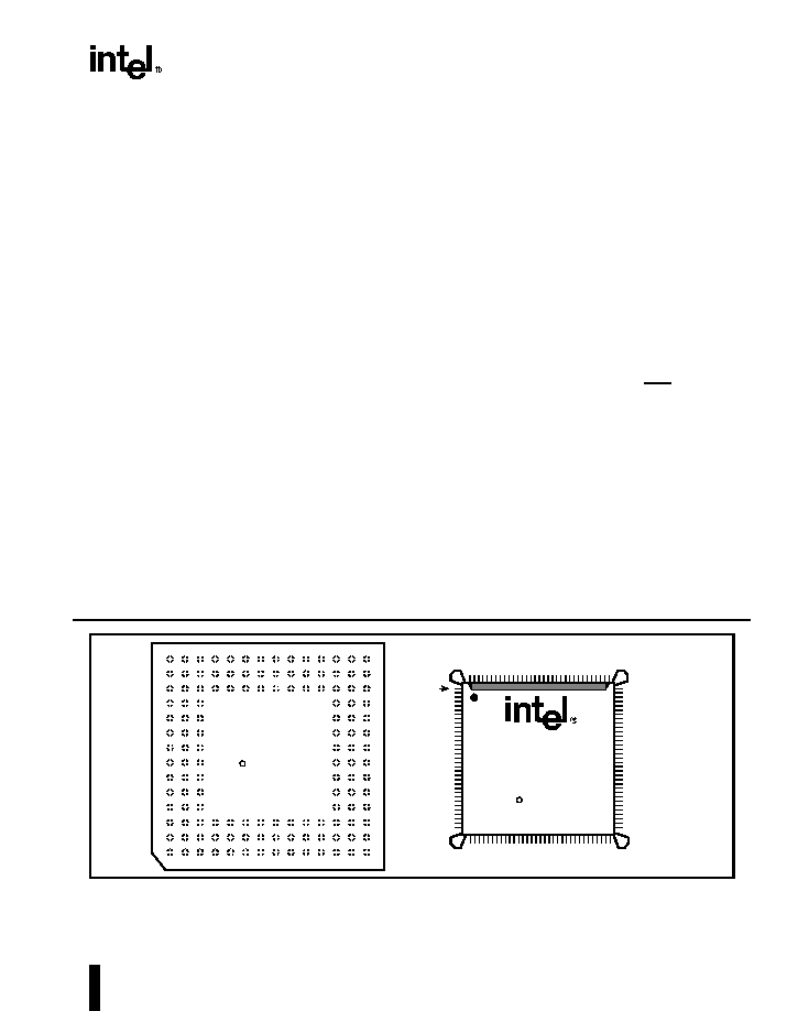
Figure 1.
80960JD Microprocessor
s
Pin/Code Compatible with all 80960Jx
Processors
s
High-Performance Embedded Architecture
-- One Instruction/Clock Execution
-- Core Clock Rate is 2x the Bus Clock
-- Load/Store Programming Model
-- Sixteen 32-Bit Global Registers
-- Sixteen 32-Bit Local Registers (8 sets)
-- Nine Addressing Modes
-- User/Supervisor Protection Model
s
Two-Way Set Associative Instruction Cache
-- 80960JD - 4 Kbyte
-- Programmable Cache Locking
Mechanism
s
Direct Mapped Data Cache
-- 80960JD - 2 Kbyte
-- Write Through Operation
s
On-Chip Stack Frame Cache
-- Seven Register Sets Can Be Saved
-- Automatic Allocation on Call/Return
-- 0-7 Frames Reserved for High-Priority
Interrupts
s
On-Chip Data RAM
-- 1 Kbyte Critical Variable Storage
-- Single-Cycle Access
s
3.3 V Supply Voltage
-- 5 V Tolerant Inputs
-- TTL Compatible Outputs
s
High Bandwidth Burst Bus
-- 32-Bit Multiplexed Address/Data
-- Programmable Memory Configuration
-- Selectable 8-, 16-, 32-Bit Bus Widths
-- Supports Unaligned Accesses
-- Big or Little Endian Byte Ordering
s
High-Speed Interrupt Controller
-- 31 Programmable Priorities
-- Eight Maskable Pins plus NMI
-- Up to 240 Vectors in Expanded Mode
s
Two On-Chip Timers
-- Independent 32-Bit Counting
-- Clock Prescaling by 1, 2, 4 or 8
-- lnternal Interrupt Sources
s
Halt Mode for Low Power
s
IEEE 1149.1 (JTAG) Boundary Scan
Compatibility
s
Packages
-- 132-Lead Pin Grid Array (PGA)
-- 132-Lead Plastic Quad Flat Pack (PQFP)
PIN 1
132
99
66
33
i960
Æ
i
M
i
© 19xx
M
© 19xx
A80960JD
NG80960JD
XXXXXXXXC0
XXXXXXXXC0S

Information in this document is provided in connection with Intel products. No license, express or implied, by
estoppel or otherwise, to any intellectual property rights is granted by this document. Except as provided in
Intel's Terms and Conditions of Sale for such products, Intel assumes no liability whatsoever, and Intel
disclaims any express or implied warranty, relating to sale and/or use of Intel products including liability or
warranties relating to fitness for a particular purpose, merchantability, or infringement of any patent, copyright
or other intellectual property right. Intel products are not intended for use in medical, life saving, or life
sustaining applications.
Intel retains the right to make changes to specifications and product descriptions at any time, without notice.
*Third-party brands and names are the property of their respective owners.
Copies of documents which have an ordering number and are referenced in this document, or other Intel
literature, may be obtained from:
Intel Corporation
P.O. Box 7641
Mt. Prospect IL 60056-764
or call 1-800-548-4725
©INTEL CORPORATION, 1996

Contents
iii
80960JD
3.3 V EMBEDDED 32-BIT MICROPROCESSOR
1.0 PURPOSE .................................................................................................................................................. 1
2.0 80960JD OVERVIEW ................................................................................................................................ 1
2.1 80960 Processor Core ........................................................................................................................ 2
2.2 Burst Bus ............................................................................................................................................ 2
2.3 Timer Unit ........................................................................................................................................... 3
2.4 Priority Interrupt Controller ................................................................................................................. 3
2.5 Instruction Set Summary .................................................................................................................... 3
2.6 Faults and Debugging ........................................................................................................................ 3
2.7 Low Power Operation ......................................................................................................................... 3
2.8 Test Features ..................................................................................................................................... 4
2.9 Memory-Mapped Control Registers .................................................................................................... 4
2.10 Data Types and Memory Addressing Modes ................................................................................... 4
3.0 PACKAGE INFORMATION ....................................................................................................................... 6
3.1 Pin Descriptions .................................................................................................................................. 6
3.1.1 Functional Pin Definitions ........................................................................................................ 6
3.1.2 80960Jx 132-Lead PGA Pinout ............................................................................................. 12
3.1.3 80960Jx PQFP Pinout ........................................................................................................... 16
3.2 Package Thermal Specifications ...................................................................................................... 19
3.3 Thermal Management Accessories .................................................................................................. 21
4.0 ELECTRICAL SPECIFICATIONS ........................................................................................................... 22
4.1 Absolute Maximum Ratings .............................................................................................................. 22
4.2 Operating Conditions ........................................................................................................................ 22
4.3 Connection Recommendations ........................................................................................................ 22
4.4 V
CC5
Pin Requirements (V
DIFF
) ........................................................................................................ 23
4.5 VCCPLL Pin Requirements .............................................................................................................. 23
4.6 DC Specifications ............................................................................................................................. 24
4.7 AC Specifications ............................................................................................................................. 26
4.7.1 AC Test Conditions and Derating Curves .............................................................................. 29
4.7.2 AC Timing Waveforms ........................................................................................................... 30
5.0 BUS FUNCTIONAL WAVEFORMS ........................................................................................................ 37
6.0 DEVICE IDENTIFICATION ...................................................................................................................... 51
7.0 REVISION HISTORY ............................................................................................................................... 53

Contents
iv
FIGURES
Figure 1.
80960JD Microprocessor ................................................................................................................ i
Figure 2.
80960JD Block Diagram ................................................................................................................ 2
Figure 3.
132-Lead Pin Grid Array Bottom View - Pins Facing Up ............................................................. 12
Figure 4.
132-Lead Pin Grid Array Top View - Pins Facing Down .............................................................. 13
Figure 5.
132-Lead PQFP - Top View ......................................................................................................... 16
Figure 6.
VCC5 Current-Limiting Resistor ................................................................................................... 23
Figure 7.
VCCPLL Lowpass Filter ............................................................................................................... 23
Figure 8.
AC Test Load ............................................................................................................................... 29
Figure 9.
Output Delay or Hold vs. Load Capacitance ................................................................................ 29
Figure 10.
CLKIN Waveform ......................................................................................................................... 30
Figure 11.
Output Delay Waveform for T
OV1
................................................................................................ 30
Figure 12.
Output Float Waveform for T
OF
................................................................................................... 31
Figure 13.
Input Setup and Hold Waveform for T
IS1
and T
IH1
...................................................................... 31
Figure 14.
Input Setup and Hold Waveform for T
IS2
and T
IH2
...................................................................... 32
Figure 15.
Input Setup and Hold Waveform for T
IS3
and T
IH3
...................................................................... 32
Figure 16.
Input Setup and Hold Waveform for T
IS4
and T
IH4
...................................................................... 33
Figure 17.
Relative Timings Waveform for T
LX
, T
LXL
and T
LXA
.................................................................... 33
Figure 18.
DT/R and DEN Timings Waveform .............................................................................................. 34
Figure 19.
TCK Waveform ............................................................................................................................ 34
Figure 20.
Input Setup and Hold Waveforms for T
BSIS1
and T
BSIH1
............................................................. 35
Figure 21.
Output Delay and Output Float Waveform for T
BSOV1
AND T
BSOF1
............................................ 35
Figure 22.
Output Delay and Output Float Waveform for T
BSOV2
and T
BSOF2
............................................. 36
Figure 23.
Input Setup and Hold Waveform for T
BSIS2
and T
BSIH2
............................................................... 36
Figure 24.
Non-Burst Read and Write Transactions Without Wait States, 32-Bit Bus .................................. 37
Figure 25.
Burst Read and Write Transactions Without Wait States, 32-Bit Bus .......................................... 38
Figure 26.
Burst Write Transactions With 2,1,1,1 Wait States, 32-Bit Bus ................................................... 39
Figure 27.
Burst Read and Write Transactions Without Wait States, 8-Bit Bus ............................................ 40
Figure 28.
Burst Read and Write Transactions With 1, 0 Wait States
and Extra Tr State on Read, 16-Bit Bus ....................................................................................... 41
Figure 29.
Bus Transactions Generated by Double Word Read Bus Request,
Misaligned One Byte From Quad Word Boundary, 32-Bit Bus, Little Endian .............................. 42
Figure 30.
HOLD/HOLDA Waveform For Bus Arbitration ............................................................................. 43
Figure 31.
Cold Reset Waveform .................................................................................................................. 44
Figure 32.
Warm Reset Waveform ................................................................................................................ 45
Figure 33.
Entering the ONCE State ............................................................................................................. 46
Figure 34.
Summary of Aligned and Unaligned Accesses (32-Bit Bus) ........................................................ 49
Figure 35.
Summary of Aligned and Unaligned Accesses (32-Bit Bus) (Continued) .................................... 50
Figure 36.
80960JD Device Identification Register ....................................................................................... 51

Contents
v
TABLES
Table 1.
80960Jx Instruction Set ................................................................................................................. 5
Table 2.
Pin Description Nomenclature ....................................................................................................... 6
Table 3.
Pin Description -- External Bus Signals ........................................................................................ 7
Table 4.
Pin Description -- Processor Control Signals, Test Signals and Power ..................................... 10
Table 5.
Pin Description -- Interrupt Unit Signals ..................................................................................... 11
Table 6.
132-Lead PGA Pinout -- In Signal Order .................................................................................... 14
Table 7.
132-Lead PGA Pinout -- In Pin Order ......................................................................................... 15
Table 8.
132-Lead PQFP Pinout -- In Signal Order .................................................................................. 17
Table 9.
132-Lead PQFP Pinout -- In Pin Order ....................................................................................... 18
Table 10.
132-Lead PGA Package Thermal Characteristics ....................................................................... 19
Table 11.
132-Lead PQFP Package Thermal Characteristics ..................................................................... 20
Table 12.
Maximum T
A
at Various Airflows in ∞C ......................................................................................... 21
Table 13.
80960JD Operating Conditions .................................................................................................... 22
Table 14.
80960JD DC Characteristics ....................................................................................................... 24
Table 15.
80960JD ICC Characteristics ...................................................................................................... 25
Table 16.
80960JD AC Characteristics ........................................................................................................ 26
Table 17.
Note Definitions for Table 16, 80960JD AC Characteristics (pg. 26) ........................................... 28
Table 18.
Natural Boundaries for Load and Store Accesses ....................................................................... 47
Table 19.
Summary of Byte Load and Store Accesses ............................................................................... 47
Table 20.
Summary of Short Word Load and Store Accesses .................................................................... 47
Table 21.
Summary of n-Word Load and Store Accesses (n = 1, 2, 3, 4) ................................................... 48
Table 22.
80960JD66 Die and Stepping Reference .................................................................................... 51
Table 23.
Fields of 80960JD Device ID ....................................................................................................... 52
Table 24.
80960JD Device ID Model Types ................................................................................................ 52
Table 25.
Device ID Version Numbers for Different Steppings .................................................................... 52