As of May 2001, this document replaces the Basis Corp. document
CD1400 Data Book.
May 2001
CD1400
UXART Serial/Parallel Controller
Datasheet
The CD1400 is a flexible asynchronous receiver/transmitter with four full-duplex serial
channels, or three full-duplex serial channels and one high-speed bidirectional parallel channel.
With optional special character processing capabilities, it is especially well-suited for UNIX
applications. The CD1400 is fabricated in an advanced-CMOS process and operates on a system
clock of up to 60 MHz. Packaged in a 100-pin MQFP, its high throughput, low-power
consumption and high level of integration permit system designs with minimum part-count,
maximum performance and maximum reliability.
Note:
This document applies to the CD1400 Revision J or later device.
Note:
The CD1400 is only offered in a 100-pin MQFP package.
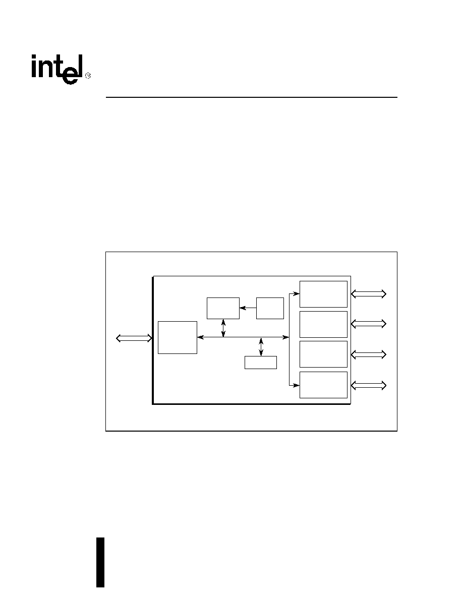
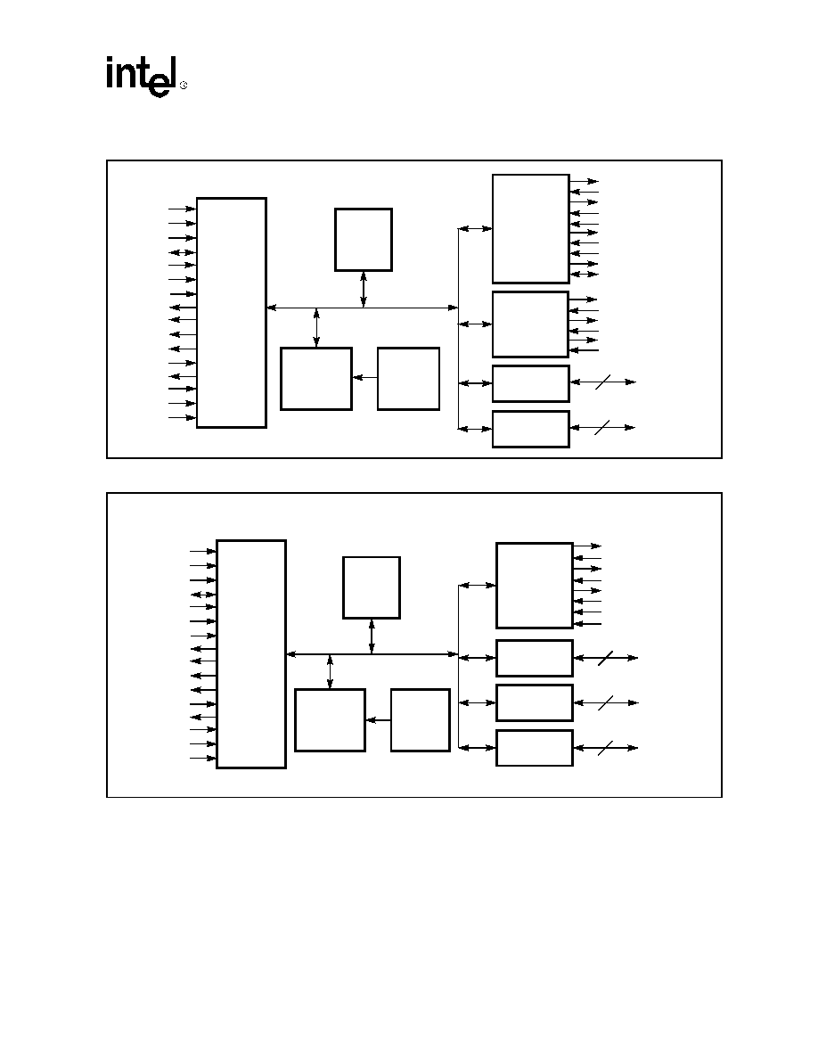
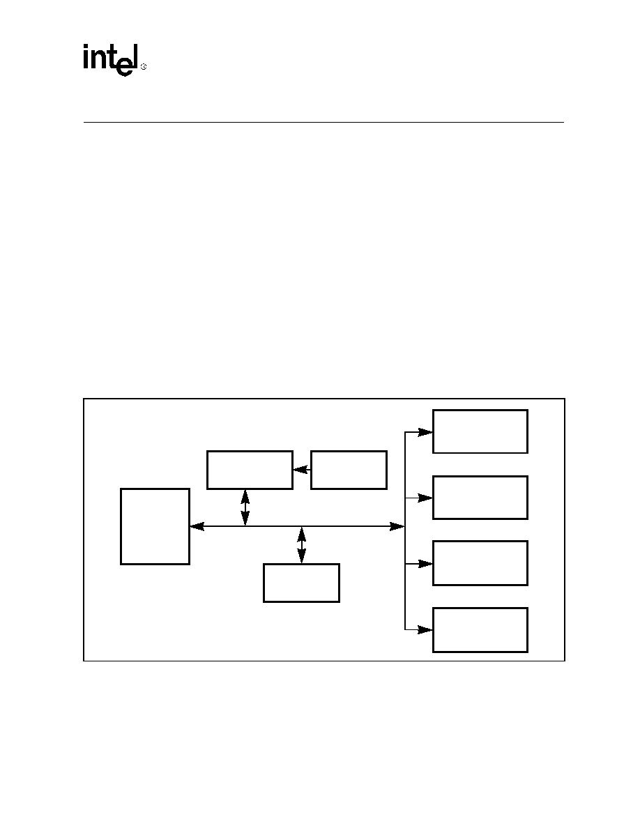
Figure 1. Functional Block Diagram
A8661-01
Host
Interface
Serial/Parallel
Interface
Channels
Firmware
ROM
User-Configurable
Channel 0
Serial / Parallel
User-Configurable
Channel 1
Serial
User-Configurable
Channel 2
Serial
User-Configurable
Channel 3
Serial
RAM
RISC
Processor
Host Bus
Interface
Logic

Datasheet
Information in this document is provided in connection with Intel
Æ
products. No license, express or implied, by estoppel or otherwise, to any intellectual
property rights is granted by this document. Except as provided in Intel's Terms and Conditions of Sale for such products, Intel assumes no liability
whatsoever, and Intel disclaims any express or implied warranty, relating to sale and/or use of Intel products including liability or warranties relating to
fitness for a particular purpose, merchantability, or infringement of any patent, copyright or other intellectual property right. Intel products are not
intended for use in medical, life saving, or life sustaining applications.
Intel may make changes to specifications and product descriptions at any time, without notice.
Designers must not rely on the absence or characteristics of any features or instructions marked "reserved" or "undefined." Intel reserves these for
future definition and shall have no responsibility whatsoever for conflicts or incompatibilities arising from future changes to them.
The CD1400 may contain design defects or errors known as errata which may cause the product to deviate from published specifications. Current
characterized errata are available on request.
Contact your local Intel sales office or your distributor to obtain the latest specifications and before placing your product order.
Copies of documents which have an ordering number and are referenced in this document, or other Intel literature may be obtained by calling 1-800-
548-4725 or by visiting Intel's website at http://www.intel.com.
Copyright © Intel Corporation, 2001
*Third-party brands and names are the property of their respective owners.

Datasheet
3
UXART Serial/Parallel Controller -- CD1400
Contents
1.0
Features
......................................................................................................................... 9
1.1
Asynchronous Features ........................................................................................ 9
1.2
Parallel Features ................................................................................................. 10
2.0
Configuration Examples
........................................................................................ 10
3.0
Design Considerations
.......................................................................................... 10
3.1
Pin Differences .................................................................................................... 10
4.0
Conventions
............................................................................................................... 11
4.1
Abbreviations....................................................................................................... 11
4.2
Acronyms ............................................................................................................12
5.0
Pin Information
.......................................................................................................... 14
5.1
Pin Functions - Major Operational Modes ........................................................... 15
5.2
Pin List................................................................................................................. 16
6.0
Registers
...................................................................................................................... 22
6.1
CD1400 Register Map.........................................................................................23
6.2
Register Definitions ............................................................................................. 24
7.0
Functional Description
........................................................................................... 29
7.1
Device Architecture ............................................................................................. 29
7.2
Host Interface ......................................................................................................30
7.2.1
Host Read Cycles................................................................................... 31
7.2.2
Host Write Cycles................................................................................... 31
7.2.3
Host Service Acknowledge Cycles......................................................... 32
7.3
Service Requests ................................................................................................ 32
7.3.1
Interrupt .................................................................................................. 33
7.3.2
Polling..................................................................................................... 36
7.3.3
Service Requests and Multiple CD1400s............................................... 37
7.4
Serial Data Reception and Transmission ............................................................ 38
7.4.1
Receiver Operation ................................................................................ 40
7.4.2
Receiver Timer Operations .................................................................... 40
7.4.3
Receive Exceptions................................................................................ 41
7.4.4
Transmitter Operation ............................................................................42
7.4.5
Transmitter Timer Operations ................................................................ 43
7.5
Flow Control ........................................................................................................ 45
7.5.1
In-Band Flow Control.............................................................................. 45
7.5.2
Out-of-Band Flow Control....................................................................... 47
7.5.3
Modem Signals and General-Purpose I/O ............................................. 48
7.6
Receive Special Character Processing ...............................................................50
7.6.1
UNIX Character Processing ................................................................... 51
7.6.2
Non-UNIX Receive Special Character Processing................................. 52
7.7
Transmit Special Character Processing .............................................................. 56
7.7.1
Line Terminating Characters .................................................................. 56
7.7.2
Embedded Transmit Commands............................................................ 56

CD1400 -- UXART Serial/Parallel Controller
4
Datasheet
7.7.3
Send Special Character Command........................................................ 57
7.8
Baud Rate Generation ........................................................................................ 61
7.9
Diagnostic Facilities -- Loopback ....................................................................... 62
7.10
Parallel Channel Operations ............................................................................. 62
7.10.1 Transmit Operation ................................................................................ 63
7.10.2 Receive Operation ................................................................................. 64
7.10.3 Programming Considerations................................................................. 65
7.11
Hardware Configurations .................................................................................... 66
7.11.1 Interfacing to an Intel Microprocessor-Based System............................ 67
7.11.2 Interfacing to a Motorola* Microprocessor-Based System ..................... 67
7.11.3 Interfacing to a National Semiconductor* Microprocessor-Based System .
67
8.0
Programming
............................................................................................................. 71
8.1
Overview ............................................................................................................. 71
8.2
Initialization ......................................................................................................... 71
8.2.1
Chip Initialization .................................................................................... 71
8.2.2
Global Function Initialization .................................................................. 73
8.2.3
Individual Channel Initialization .............................................................. 74
8.3
Poll Mode Examples ........................................................................................... 75
8.3.1
Polling Routine Examples ...................................................................... 76
8.4
Hardware-Activated Service Examples............................................................... 80
8.4.1
Receive Service ..................................................................................... 80
8.4.2
Transmit Service .................................................................................... 81
8.4.3
Modem Service ...................................................................................... 82
8.4.4
Baud Rate Derivation ............................................................................. 83
8.5
Baud Rate Tables ............................................................................................... 84
8.6
ASCII Code Table ............................................................................................... 86
8.6.1
Hexadecimal -- Character ..................................................................... 86
8.6.2
Decimal -- Character ............................................................................. 86
9.0
Detailed Register Descriptions
........................................................................... 88
9.1
Global Registers.................................................................................................. 88
9.1.1
Global Firmware Revision Code (GFRCR) ............................................ 88
9.1.2
Channel Access Register (CAR) ............................................................ 88
9.1.3
Global Configuration Register (GCR)..................................................... 89
9.1.4
Service Request Register (SVRR) ......................................................... 90
9.1.5
Receive Interrupting Channel Register (RICR) ...................................... 90
9.1.6
Transmit Interrupting Channel Register (TICR)...................................... 90
9.1.7
Modem Interrupting Channel Register (MICR)....................................... 91
9.1.8
Receive Interrupt Register (RIR) ............................................................ 92
9.1.9
Transmit Interrupt Register (TIR) ........................................................... 92
9.1.10 Modem Interrupt Register (MIR)............................................................. 92
9.1.11 Prescaler Period Register (PPR)............................................................ 93
9.2
Virtual Registers.................................................................................................. 94
9.2.1
Receive Interrupt Vector Register (RIVR) .............................................. 94
9.2.2
Transmit Interrupt Vector Register (TIVR).............................................. 94
9.2.3
Modem Interrupt Vector Register (MIVR)............................................... 95
9.2.4
Transmit Data Register (TDR)................................................................ 96
9.2.5
Receive Data/Status Register (RDSR)................................................... 96

Datasheet
5
UXART Serial/Parallel Controller -- CD1400
9.2.6
Receive Data/Status Register (RDSR)................................................... 96
9.2.7
Modem Interrupt Status Register (MISR) ............................................... 98
9.2.8
End Of Service Request Register (EOSRR) .......................................... 98
9.3
Channel Registers...............................................................................................99
9.3.1
Local Interrupt Vector Register (LIVR) ................................................... 99
9.3.2
Channel Command Register (CCR) ....................................................... 99
9.3.3
Service Request Enable Register (SRER) ........................................... 104
9.4
Channel Option Registers ................................................................................. 105
9.4.1
Channel Option Register 1 (COR1)...................................................... 105
9.4.2
Channel Option Register 2 (COR2)...................................................... 107
9.4.3
Channel Option Register 3 (COR3) Serial Format ............................... 108
9.4.4
Channel Option Register 3 (COR3) Parallel Format ............................ 108
9.4.5
Channel Option Register 4 (COR4)...................................................... 110
9.4.6
Channel Option Register 5 (COR5)...................................................... 111
9.4.7
Channel Control Status Register (CCSR) Serial Format......................112
9.4.8
Channel Control Status Register (CCSR) Parallel Format ................... 112
9.4.9
Received Data Count Register (RDCR) Serial Format ........................ 114
9.4.10 Received Data Count Register (RDCR) Parallel Format......................114
9.5
Special Character Registers.............................................................................. 116
9.5.1
Special Character Register 1 (SCHR1) ................................................116
9.5.2
Special Character Register 2 (SCHR2) ................................................116
9.5.3
Special Character Register 3 (SCHR3) ................................................116
9.5.4
Special Character Register 4 (SCHR4) ................................................117
9.5.5
Special Character Range Low (SCRL)................................................. 117
9.5.6
Special Character Range High (SCRH) ............................................... 117
9.5.7
LNext Character (LNC)......................................................................... 118
9.6
Modem Change Option Registers ..................................................................... 118
9.6.1
Modem Change Option Register 1 (MCOR1) Serial Format ................118
9.6.2
Modem Change Option Register 1 (MCOR1) Parallel Format ............. 119
9.6.3
Modem Change Option Register 2 (MCOR2) Serial Format ................120
9.6.4
Modem Change Option Register 2 (MCOR2) Parallel Format ............. 120
9.6.5
Receive Time-out Period Register (RTPR) ..........................................121
9.6.6
Modem Signal Value Register 1 (MSVR1 ............................................ 122
9.6.7
Modem Signal Value Register 2 (MSVR2) ........................................... 122
9.6.8
Printer Signal Value Register (PSVR) .................................................. 122
9.6.9
Receive Baud Rate Period Register (RBPR) ....................................... 123
9.6.10 Receive Clock Option Register (RCOR) .............................................. 124
9.6.11 Transmit Baud Rate Period Register (TBPR)....................................... 124
9.6.12 Transmit Clock Option Register (TCOR) .............................................. 125
10.0
Electrical Specifications
...................................................................................... 126
10.1
Absolute Maximum Ratings............................................................................... 126
10.2
Recommended Operating Conditions ............................................................... 126
10.3
DC Electrical Characteristics............................................................................. 126
10.4
AC Electrical Characteristics ............................................................................. 128
10.4.1 Index of Timing Information .................................................................. 128
10.4.2 Asynchronous Timing........................................................................... 128
10.4.3 Synchronous Timing............................................................................. 132
10.4.4 Parallel Port Timing Specifications....................................................... 135

CD1400 -- UXART Serial/Parallel Controller
6
Datasheet
11.0
Package Specifications
....................................................................................... 138
11.1
100-Pin MQFP (JEDEC) Package .................................................................... 138
12.0
Ordering Information
............................................................................................ 139
12.1
Pin Diagram -- 100-Pin MQFP ......................................................................... 140
13.0
Quick Reference
..................................................................................................... 141
13.1
CD1400 Register Map....................................................................................... 141
Figures
1
Workstation: Printer, Keyboard, Mouse and Modem Ports ................................. 12
2
Three Serial Ports and One Bidirectional Parallel Port ....................................... 13
3
Four Full-Modem Ports ....................................................................................... 13
4
Pin Diagram -- CD1400...................................................................................... 14
5
Pin Functions -- Four Serial Channel Mode ....................................................... 15
6
Pin Functions -- Three Serial/One Parallel Channel Mode ................................ 16
7
CD1400 Functional Block Diagram ..................................................................... 29
8
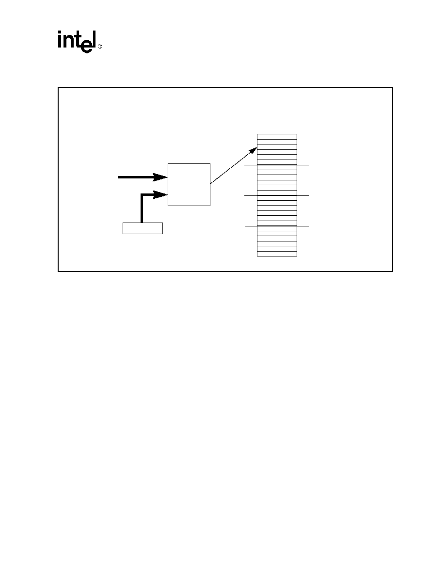
Internal Address Generation ............................................................................... 31
9
Control Signal Generation ................................................................................... 34
10
CD1400 Daisy-Chain Connections ..................................................................... 38
11
FIFO Timer Processing ....................................................................................... 44
12
CD1400 Receive Character Processing ............................................................. 53
13
CD1400 Transmit Character Processing ............................................................ 59
14
CD1400 Parallel Data Transmit Connections ..................................................... 64
15
CD1400 Parallel Data Receive Connections ...................................................... 65
16
Relationship between RCOR/RBPR and PACK* Pulse ...................................... 66
17
Intel, 80x86 Family Interface ............................................................................... 68
18
Motorola* 68020 Interface ................................................................................... 69
19
National* 32000 Interface.................................................................................... 70
20
CD1400 Master Initialization Sequence .............................................................. 73
21
Reset Timing ..................................................................................................... 129
22
Clock Timing ..................................................................................................... 130
23
Asynchronous Read Cycle Timing .................................................................... 130
24
Asynchronous Write Cycle Timing .................................................................... 131
25
Asynchronous Service Acknowledge Cycle Timing .......................................... 132
26
Synchronous Read Cycle Timing ...................................................................... 133
27
Synchronous Write Cycle Timing ...................................................................... 134
28
Synchronous Service Acknowledge Cycle Timing ............................................ 135
29
Parallel Port Transmit Timing ............................................................................ 137
30
Parallel Port Receive Timing ............................................................................. 137
31
Pin Diagram -- 100-Pin MQFP ......................................................................... 140

Datasheet
7
UXART Serial/Parallel Controller -- CD1400
Tables
1
General................................................................................................................ 16
2
Microprocessor Interface..................................................................................... 17
3
Service Request Interface ................................................................................... 17
4
Communication Interface .................................................................................... 17
5
Miscellaneous......................................................................................................18
6
Pin Descriptions .................................................................................................. 19
7
Global Registers.................................................................................................. 23
8
Virtual Registers .................................................................................................. 23
9
Channel Registers...............................................................................................23
10
Global Registers.................................................................................................. 24
11
Virtual Registers .................................................................................................. 25
12
Channel Registers...............................................................................................26
13
Modem Registers ................................................................................................ 27
14
Baud Rate Constants, CLK = 60 MHz................................................................. 84
15
Baud Rate Constants, CLK = 25 MHz................................................................. 84
16
Baud Rate Constants, CLK = 20.2752 MHz........................................................ 85
17
Receive/Transmit/Modem Interrupting Channel Registers.................................. 91
18
Receive/Transmit/Modem Interrupt Vector Registers ......................................... 95
19
Receive Data/Status Register ............................................................................. 97
20
Global Registers................................................................................................ 141
21
Virtual Registers ................................................................................................ 141
22
Channel Registers.............................................................................................141
23
Bit Definitions ....................................................................................................142

CD1400 -- UXART Serial/Parallel Controller
8
Datasheet
Revision History
Revision
Date
Description
1.0
May 2001
Initial release.

UXART Serial/Parallel Controller -- CD1400
Datasheet
9
1.0
Features
1.1
Asynchronous Features
∑
Software-programmable serial data rates up to 230.4 kbps, full-duplex
Note:
A minimum clock frequency of 60 MHz is required to run all four serial channels at a 230.4-kbps
data rate. Refer to the AC characteristics (
"Electrical Specifications" on page 126
) for complete
information on device timing.
∑
Twelve bytes of FIFO for each transmitter and each receiver, with programmable threshold for
receive-FIFO-interrupt generation
∑
Improved interrupt schemes: Good Data
interrupts eliminate the need for character status
check
∑
Independent bit rate selection for transmit and receive on each channel
∑
User-programmable and automatic flow control modes for the serial channels:
-- In-band (software) flow control via single character (XON/XOFF)
-- Out-of-band (hardware) flow control via RTS/CTS and DTR/DSR
∑
Special character recognition and generation
∑
Special character processing, particularly useful for UNIX-line-driver applications, optionally
handled automatically by the CD1400
-- Automatic expansion of NL to CR-NL
-- Supports LNEXT and ISTRIP
-- Ignore Break
-- UNIX parity handling options:
Character removed from stream
Passed as Good Data
Replaced with null (00 hex)
Preceded with FF-00 hex
Passed as is with exception flagged
∑
Line break detection (start and end) and generation, with programmable choice of response
and data pattern to the host
∑
Insertion of transmit delays in data stream
∑
One timer per channel for receive data time-out interrupt
∑
Six modem control signals-per-channel (DTRDSR, RTS, CTS, CD, RI); CD and RI Signals
not available if using the parallel channel
∑
Local and Remote Maintenance Loopback Modes
∑
Five to eight data bits per character plus optional parity
∑
Odd, even, no, or forced parity
∑
1, 1.5, or 2 Stop bits
CD1400 -- UXART Serial/Parallel Controller
10
Datasheet
1.2
Parallel Features
∑
Parallel data rates up to 105-Kbytes/sec. receive and 32-Kbytes/sec. transmit
∑
Thirty-byte FIFO
∑
Programmable strobe pulse widths
∑
Automatic generation and recognition of handshake control signals (STROBE, ACK, BUSY)
∑
Compatible with Centronics
-interface specifications
∑
New bits provided to increase parallel signal width
2.0
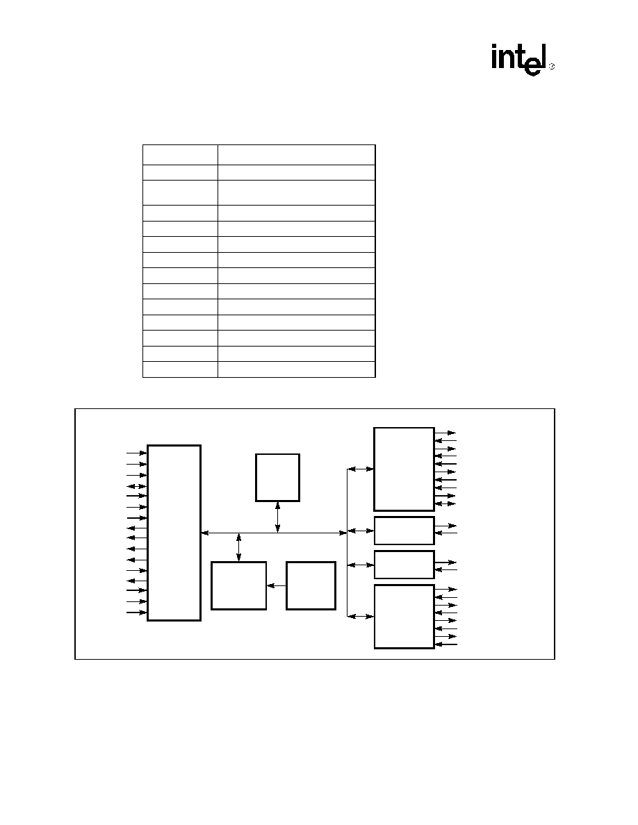
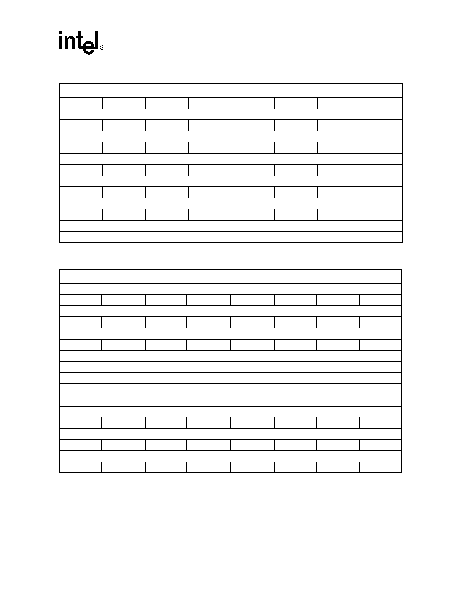
Configuration Examples
Figure 1 on page 12
through
Figure 3 on page 13
are functional block diagrams of three possible
configurations that can be implemented with the CD1400. The first is a typical workstation with
printer, mouse, keyboard and modem ports, a mode that includes a single parallel port and three
serial channels with modem control;
Figure 2
illustrates one channel with complete bidirectional
modem control and three channels with partial modem control;
Figure 3
shows a quad serial mode
of four channels with complete modem control. All modes of operation are software-
programmable through Control registers within the CD1400.
3.0
Design Considerations
The CD1400 Revision J is a higher speed version of the CD1400 Revision G. The CD1400
Revision J is only available in a 100-pin MQFP package.
It is recommended that the CD1400 Revision J be used for any new designs. Please note that to
achieve the high data rates, a 60-MHz clock is required. Please refer to the pin differences between
the CD1400 Revision G and J.
3.1
Pin Differences
Feature
CD1400 Revision J
CD1400 Revision G
Package
100-pin MQFP
100-pin MQFP
System clock
60 MHz
25 MHz
Maximum bit rates
230.4 kbps
115.2 kbps
Ground pins
13
4
V
CC
pins
8
3
No-connect pins
15
29
UXART Serial/Parallel Controller -- CD1400
Datasheet
11
Notes:
1. Some of the no-connect pins on the CD1400 Revision G (100-pin MQFP) were converted to
additional V
CC
and ground pins on the CD1400 Revision J (please refer to the
"Pin List" on
page 16
for details).
2. The CD1400 Revision G part does not work in a Revision J layout. The Revision G no-
connect pins must be left as true no-connect pins and cannot be connected to V
CC
or Ground.
3. To achieve the high data rates, a 60-MHz system clock is required. However, it is not possible
to achieve some low bit rates based on a 60-MHz clock (a lower system clock is required).
Refer to
"Baud Rate Tables" on page 84
for bit-rate programming constraints.
Higher clock rates produce shorter PSTROBE* signal pulse widths, so when Channel 0 is
programmed as a parallel port, similar limitations must also be considered (see
" Parallel
Channel Operations" on page 62
for PSTROBE* pulse-width programming constraints).
4.0
Conventions
4.1
Abbreviations
The use of `tbd' indicates values that are `to be determined', `n/a' designates `not available', and
`n/c' indicates a pin that is a `no connect'.
Symbol
Units of measure
∞
C
degree Celsius
µ
F
microfarad
µ
s
microsecond (1,000 nanoseconds)
Hz
hertz (cycle per second)
Kbit
kilobit (1,024 bits)
kbps
kbits/second
kilobit (1,000 bits) per second
Kbyte
kilobyte (1,024 bytes)
Kbytes/sec.
kilobyte (1,000 bytes) per second
kHz
kilohertz
k
kilohm
Mbyte
megabyte (1,048,576 bytes)
MHz
megahertz (1,000 kilohertz)
mA
milliampere
ms
millisecond (1,000 microseconds)
ns
nanosecond
pV
picovolt
V
volt
W
watt
CD1400 -- UXART Serial/Parallel Controller
12
Datasheet
4.2
Acronyms
Acronym
Definition
AC
alternating current
CMOS
complementary metal-oxide
semiconductor
DC
direct current
DRAM
dynamic random-access memory
FIFO
first in/first out
ISA
industry standard architecture
LSB
least-significant bit
MSB
most-significant bit
MQFP
metric quad-flat pack
RAM
random-access memory
R/W
read/write
SDLC
synchronous data link control
TTL
transistor-transistor logic
Figure 1. Workstation: Printer, Keyboard, Mouse and Modem Ports
PD[7:0]
PARALLEL
SERIAL
CHANNEL 3
RAM
AND
FIFOS
FIRMWARE
ROM
RESET*
CLK
A[6:0]
DB[7:0]
R/W*
CS*
DS*
DTACK*
SVCREQR*
SVCREQT*
SVCREQM*
DGRANT*
DPASS*
SVCACKR*
SVCACKT*
SVCACKM*
TXD1
RXD1
PSTROBE*
PACK*
PSLIN*
PSLCT*
PBUSY
PINIT*
PERROR*
PPE*
PAUTOFD*
SERIAL
CHANNEL 2
RISC
PROCESSOR
PRINTER
OR
SCANNER
SERIAL
CHANNEL 1
MOUSE
TXD2
RXD2
TXD3
RXD3
RTS3*
CTS3*
DTR3*
DSR3*
GPO[3:0]
GPI[3:0]
MODEM
KEYBOARD
HOST
BUS
INTERFACE
LOGIC
CHANNEL
UXART Serial/Parallel Controller -- CD1400
Datasheet
13
Figure 2. Three Serial Ports and One Bidirectional Parallel Port
Figure 3. Four Full-Modem Ports
PSTROBE*
PACK*
PSLIN*
PSLCT*
PBUSY
PINIT*
PERROR*
PPE*
PAUTOFD*
PD[7:0]
SERIAL
CHANNEL 2
PARALLEL
CHANNEL
SERIAL
CHANNEL 3
TXD1
RXD1
RTS1*
CTS1*
DTR1*
DSR1*
SERIAL
CHANNEL 1
RAM
FIFOS
FIRMWARE
ROM
SAME AS
CHANNEL 1
RESET*
CLK
A[6:0]
DB[7:0]
R/W*
CS*
DS*
DTACK*
SVCREQR*
SVCREQT*
SVCREQM*
DGRANT*
DPASS*
SVCACKR*
SVCACKT*
SVCACKM*
6
6
RISC
PROCESSOR
PRINTER
OR
SCANNER
SAME AS
CHANNEL 1
HOST
BUS
INTERFACE
LOGIC
AND
TXD0
RXD0
RTS0*
CTS0*
DTR0*
DSR0*
CD0*
RI0*
SERIAL
CHANNEL 3
RAM
AND
FIFOS
FIRMWARE
ROM
SAME AS
CHANNEL 0
8
8
RISC
PROCESSOR
SERIAL
CHANNEL 2
SERIAL
CHANNEL 1
SERIAL
CHANNEL 0
SAME AS
CHANNEL 0
SAME AS
CHANNEL 0
8
RESET*
CLK
A[6:0]
DB[7:0]
R/W*
CS*
DS*
DTACK*
SVCREQR*
SVCREQT*
SVCREQM*
DGRANT*
DPASS*
SVCACKR*
SVCACKT*
SVCACKM*
HOST
BUS
INTERFACE
LOGIC
CD1400 -- UXART Serial/Parallel Controller
14
Datasheet
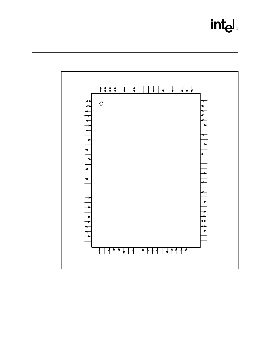
5.0
Pin Information
Note:
N/C means no connection (make no connections to these pins).
Figure 4. Pin Diagram -- CD1400
84
85
86
87
88
89
90
91
92
93
94
95
96
97
98
99
100
1
2
3
4
5
6
7
8
9
10
11
12
13
14
15
16
17
83
82
81
CD1400
100-Pin MQFP
GN
D
A[
2
]
N/
C
A[
1
]
N/
C
A[
0
]
N/C
GND
N/
C
DB
[7
]
VCC
DB[6
]
GND
DB
[
5
]
DB[4
]
DB
[
2
]
DB[1]
DB[0]
TXD0
RXD0
TXD1
RXD1
TXD2
VCC
RXD2
N/C
TXD3
GND
RXD3
N/C
DTR3*
GND
RTS3*
A[6]
RESET*
CS*
DS*
R/W*
DTACK*
N/C
CLK
GND
N/C
DPASS*
DGRANT*
N/C
GND
VCC
N/C
SVCREQM*
18
19
20
21
22
23
24
25
26
27
28
29
30
80
79
78
77
76
75
74
73
72
71
70
69
68
67
66
65
64
63
62
61
60
59
58
57
56
55
54
53
52
51
47
46
45
44
43
42
41
40
39
38
37
36
35
34
33
32
31
48
49
50
DB
[
3
]
A[
3
]
A[
4
]
A[
5
]
N/C
VCC
N/C
CTS3*
N/C
DSR3*
GND
RI3*
DTR2*
CD3*
RTS2*
CTS2*
VCC
SVCREQT*
N/C
SVCREQR*
GND
SVCACKM*
VCC
SVCACKT*
SVCACKR*
PD[0]
PD[1]
PAUTOFD*
N/C
GND
DSR0
*
CT
S0
*
RT
S0
*
GND
DT
R0
*
CD1
*
RI1
*
DSR1
*
VCC
CT
S1
*
GND
RT
S
1
*
DT
R1
*
CD2
*
RI2
*
DSR2
*
GND
RI
0
*
CD0
*
VCC
UXART Serial/Parallel Controller -- CD1400
Datasheet
15
5.1
Pin Functions - Major Operational Modes
Figure 5. Pin Functions -- Four Serial Channel Mode
TXD
RXD
DTR
DSR
RTS
CTS
RI
CD
Cha
nne
l
0
Ch
an. 1
Chan.
2
Chan.
3
8
8
8
A[6:0]
DB[7:0]
CLK
CS*
DS*
R/W*
DTACK*
DGRANT*
DPASS*
SVCREQR*
SVCREQT*
SVCREQM*
SVCACKR*
SVCACKT*
SVCACKM*
RESET*
Host
I
n
terface
Dai
s
y
Chain
Req
u
est
Se
r
v
i
c
e
Se
r
v
ice
Ac
k
CD1400 -- UXART Serial/Parallel Controller
16
Datasheet
5.2
Pin List
The following naming conventions are used in the pin assignment tables: (*) after a name denotes
an active-low signal. Signal names in parentheses are for the parallel channel.
I = input; I/O = input/output; O = output; OD = open drain.
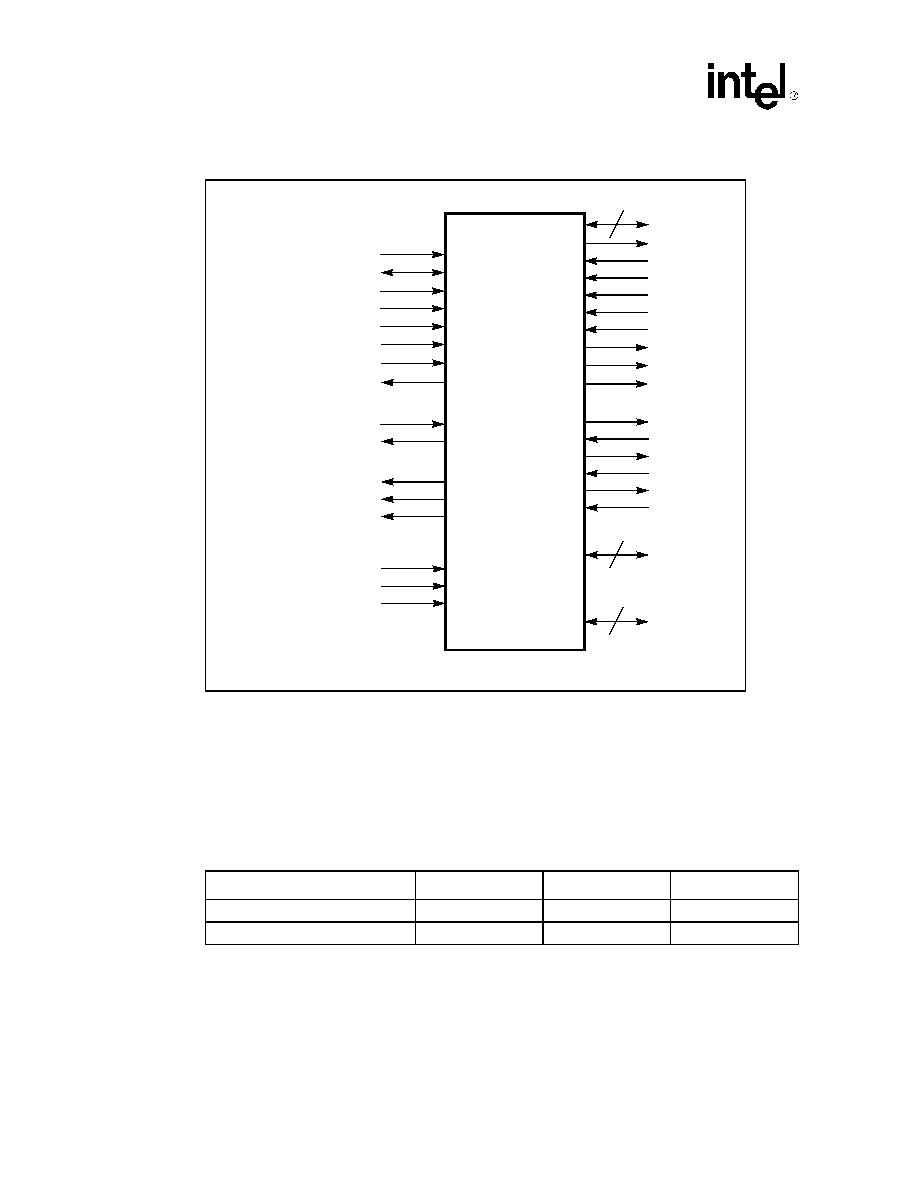
Figure 6. Pin Functions -- Three Serial/One Parallel Channel Mode
TXD
RXD
DTR
DSR
RTS
CTS
Chann
e
l 0
Chan
. 1
Chan
. 2
Ch
an. 3
6
A[6:0]
DB[7:0]
CLK
CS*
DS*
R/W*
DTACK*
DGRANT*
DPASS*
SVCREQR*
SVCREQT*
SVCREQM*
SVCACKR*
SVCACKT*
SVCACKM*
RESET*
Host
I
n
terface
Dai
s
y
Chain
Req
u
est
Ser
v
i
c
e
Ser
v
i
c
e
Ac
k
8
PD[7:0]
PSTROBE*
PACK*
PSLCT*
PBUSY
PPE*
PERROR*
PSLIN*
PINIT*
PAUTOFD*
6
Table 1. General
Symbol
Pin #
# of Pins
Type
RESET*
79
1
I
CLK
73
1
I
UXART Serial/Parallel Controller -- CD1400
Datasheet
17
Table 2. Microprocessor Interface
Symbol
Pin #
# of Pins
Type
CS*
78
1
I
DS*
77
1
I
R/W*
76
1
I
DTACK*
75
1
OD
A[6:0]
80≠83, 85, 87, 89
7
I
DB[7:0]
93, 95,
97≠100, 1, 2
8
I/O
Table 3. Service Request Interface
Symbol
Pin #
# of Pins
Type
SVCREQR*
61
1
OD
SVCREQT*
63
1
OD
SVCREQM*
65
1
OD
SVCACKR*
56
1
I
SVCACKT*
57
1
I
SVCACKM*
59
1
I
DGRANT* 69
1
I
DPASS*
71
1
O
Table 4. Communication Interface (Sheet 1 of 2)
Symbol
Pin #
# of Pins
Type
TXD0 (PSTROBE*)
3
1
O
RXD0 (PACK*)
4
1
I
RTS0* (PSLIN*)
45
1
O
CTS0* (PSLCT*)
46
1
I
DSR0* (PBUSY)
47
1
I
DTR0* (PINIT*)
43
1
O
CD0* (PERROR*)
49
1
I
RI0* (PPE*)
48
1
I
PAUTOFD*
53
1
O
TXD1
5
1
O
RXD1
6
1
I
RTS1*
36
1
O
CTS1*
38
1
I
DSR1*
40
1
I
DTR1*
35
1
O
CD1400 -- UXART Serial/Parallel Controller
18
Datasheet
CD1* (PD[2])
42
1
I/O
RI1* (PD[3])
41
1
I/O
TXD2
7
1
O
RXD2
9
1
I
RTS2*
28
1
O
CTS2*
29
1
I
DSR2*
31
1
I
DTR2*
27
1
O
CD2* (PD[4])
34
1
I/O
RI2* (PD[5])
33
1
I/O
TXD3
11
1
O
RXD3
13
1
I
RTS3* 17
1
O
CTS3*
21
1
O
DSR3*
23
1
I
DTR3*
15
1
O
CD3* (PD[16])
26
1
I/O
RI3* (PD[7])
25
1
I/O
PD[0]
54
1
I/O
PD[1]
55
1
I/O
Table 5. Miscellaneous
Symbol
Pin #
# of Pins
Type
V
CC
8, 19, 30, 39, 50, 58,
67, 94
8
≠
GND
12, 16, 24, 32, 37, 44,
51, 60, 66, 72, 84, 91,
96
13
≠
NC
10, 14, 18, 20, 22, 52,
62, 64, 68, 70, 74, 86,
88, 90, 92
15
≠
Table 4. Communication Interface (Sheet 2 of 2)

UXART Serial/Parallel Controller -- CD1400
Datasheet
19
Table 6. Pin Descriptions (Sheet 1 of 3)
Symbol
Pin No.
Type
Description
RESET*
79
I
ACTIVE-LOW RESET: This pin synchronously resets the CD1400. RESET* must be
active for a minimum of 10 system clock cycles. When RESET* is removed, the
CD1400 will perform a software initialization of its registers, disable all transmitters
and receivers, and when complete, place the firmware revision number in the
GFRCR.
CLK
73
I
CLOCK -- SYSTEM CLOCK: The CD1400 requires a nominal 60-MHz clock for
proper operation. The system clock is divided by two, internally, to generate all on-
chip timing clocks.
CS*
78
I
CHIP SELECT: When active, CS*, in conjunction with DS*, initiates a host I/O cycle
with the CD1400.
DS*
77
I
DATA STROBE: During an active I/O cycle, DS* strobes data into on-chip registers
during a write cycle or enables data onto the data bus during read cycles.
R/W*
76
I
READ/WRITE: R/W* sets the direction of the data transfer between the host and the
CD1400. When high, the cycle is a read, and when low, the cycle is a write.
DTACK*
75
OD
DATA TRANSFER ACKNOWLEDGE: When the CD1400 has completed internal
operations associated with a host I/O cycle, it activates DTACK* to indicate the end
of the cycle. The host may terminate the cycle as soon as DTACK becomes active.
A[6:0]
80≠83,
85, 87, 89
I
ADDRESS [6:0]: These signals select the on-chip register being accessed during a
host I/O cycle.
DB[7:0]
93, 95,
97≠100,
1, 2
I/O
DATA BUS [7:0]: These eight bidirectional signals are the data interface between
the host and internal CD1400 registers.
SVCREQR*
61
OD
SERVICE REQUEST RECEIVE: When the CD1400 needs host service for one of
the receivers, it activates this signal.
SVCREQT*
63
OD
SERVICE REQUEST TRANSMIT: When the CD1400 needs host service for one of
the transmitters, it activates this signal.
SVCREQM*
65
OD
SERVICE REQUEST MODEM: The CD1400 activates this signal when an enabled
change occurs.
SVCACKR*
56
I
SERVICE ACKNOWLEDGE RECEIVE: The host activates this signal to start a
receive interrupt service. This is a special-case read cycle, during which the CD1400
places the contents of the Receive Interrupt Vector register on the data bus.
SVCACKT*
57
I
SERVICE ACKNOWLEDGE TRANSMIT: The host activates this signal to start a
transmit interrupt service. This is a special-case read cycle, during which the
CD1400 places the contents of the Transmit Interrupt Vector register on the data
bus.
SVCACKM*
59
I
SERVICE ACKNOWLEDGE MODEM: The host activates this signal to start a
modem interrupt service. This is a special-case read cycle, during which the CD1400
places the contents of the Modem Interrupt Vector register on the data bus.
DGRANT*
69
I
DAISY GRANT: This input, qualified with DS* and a valid service acknowledge
(SVCACKR*, SVCACKT*, SVCACKM*), activates the CD1400 service acknowledge
cycle.
DPASS*
71
O
DAISY PASS: This output is driven low when no valid service request exists for the
type of service acknowledge active. In multiple-CD1400 designs, this signal is
normally connected to the following CD1400 DGRANT* input, forming a service
acknowledge daisy chain.
TxD[3:0]
11, 7, 5, 3
O
TRANSMIT DATA [3:0]: These output signals provide the serial transmit data
stream for all four channels. When Channel 0 is operating in Parallel Mode, TxD0
becomes PSTROBE* (See PSTROBE*).

CD1400 -- UXART Serial/Parallel Controller
20
Datasheet
RxD[3:0]
13, 9, 4
I
RECEIVE DATA [3:0]: These input signals carry the serial bit 6 bit streams into the
CD1400. When Channel 0 is programmed for parallel operation, RxD0 becomes
PACK* (See PACK*).
RTS[3:0]*
17, 28,
36, 45
O
REQUEST TO SEND [3:0]: The request to send output 3 from each channel. These
signals are controlled by the Modem Signal Value register 1 inside the CD1400.
RTS0* serves a dual-purpose based on the mode of operation of Channel 0 (see
PSLIN*).
CTS[3:0]*
21, 29,
38, 46
I
CLEAR TO SEND [3:0]: These are the clear-to-send inputs for each of the
channels. If enabled, this signal can control the transmitter, enabling transmission
when active, disabling transmission when inactive. CTS0* serves a dual-purpose
based on the mode of operation Channel 0 (see PSLCT*).
DSR[3:0]*
23, 31,
40, 47
I
DATA SET READY [3:0]: Data Set Ready for each channel. DSR0* serves a dual-
purpose based on the mode of operation of Channel 0 (see PBUSY).
DTR[3:0]*
15, 27,
35, 43
O
DATA TERMINAL READY [3:0]: Data Terminal Ready for each channel. These
signals are controlled by Modem Signal Value register 2. DTR0* serves a dual-
purpose based on the mode of operation of Channel (see PINIT*).
CD[3:0]*
PD[6],PD[4],
PD[2]
PERROR*
26, 34,
42, 49
I
CARRIER DETECT [3:0]: These are Carrier Detects for each PD[6] and PD[4]
channel and can be monitored via the Modem Signal Value registers.
CD0* serves a dual-purpose based on the mode of operation of Channel 0 (see
PERROR*).
CD1*, CD2* and CD3* serve dual purposes as Parallel Data bits 2, 4, and 6 (PD[2],
PD[4] and PD[6]) when Channel 0 is operating in Parallel mode.
RI[3:0]*
PD[7],PD[5],
PD[3],
PPE*
25, 33,
41, 48
I
RING INDICATOR [3:0]: These are the Ring Indicators for each channel and can be
monitored via the Modem Signal Value registers. RI0* serves a dual purpose based
on the mode of operation of Channel 0 (see PPE*). RI1*, RI2*, and RI3* serve dual
purposes as Parallel Data bits 3, 5, and 7 (PD[3], PD[5], and PD[7]) when Channel 0
is operating in Parallel mode.
PSTROBE*
3
O
PRINTER STROBE: This is the alternate function for TxD0 when Channel 0 is
programmed as a parallel port. When the port is selected for output (printer),
PSTROBE* is driven active by the CD1400 after a proper data setup time. Data is
held for a proper hold time after PSTROBE* is deactivated. When Channel 0 is
programmed as an input (scanner) port, PSTROBE* acts as the acknowledge pin to
signal completion of data reception.
PACK*
4
I
PRINTER ACKNOWLEDGE: This is the alternate function of RxD0 when Channel 0
is programmed as a parallel port. When the port is selected as output (printer), this
signal is used by the CD1400 to indicate completion of data reception by the printer,
and that the next I/O cycle can begin. When Channel 0 is selected as an input
(scanner), PACK* is treated as the strobe input. Proper data setup and hold times are
required.
PSLIN*
45
O
PRINTER SELECT IN
PINIT*
43
O
PRINTER INITIALIZE
PAUTOFD*
53
O
PRINTER AUTOFEED:
These three signals are general-purpose outputs. Their state is controlled by the
lower three bits of the PSVR (see the register descriptions for detailed information on
register bit assignments). PSLIN* and PINIT* are alternate functions for RTS0* and
DTR0*, depending on the mode of operation on Channel 0. PAUTOFD* is a single-
function output pin.
PSLCT*
46
I
PRINTER SELECT 0 = latch, 1 = buffer
PPE*
48
I
PRINTER PAPER EMPTY
Table 6. Pin Descriptions (Sheet 2 of 3)
Symbol
Pin No.
Type
Description
UXART Serial/Parallel Controller -- CD1400
Datasheet
21
PERROR*
49
I
PRINTER ERROR:
These three signals are general-purpose inputs. Their state can be monitored via the
upper four bits of the PSVR. As with their modem input counterparts (CTS0*, RI0*,
and CD0*), a change in state can be programmed to generate SVCREQM*. The
function of these signals is selected automatically based on the mode of operation
programmed for Channel 0.
If PSLCT* input is at logic `0', the parallel port operates as a latch. The falling edge of
the strobe input latches the data. If PSLCT* is logic `1', the input port is a buffer.
PBUSY
47
I/O
PRINTER BUSY: PBUSY is a bidirectional signal; it is an input when transmit is
enabled and an output when receive is enabled. During receive data operations, the
CD1400 drives PBUSY active after receiving the strobe from the remote. When the
device has taken the data, it deasserts PBUSY and activates PACK*. During transmit
data operations, the state of PBUSY is made available to the host via the PSVR;
however, it does not affect transfer operation and is not a handshake signal for this
direction.
PD[0]
54
I/O
PARALLEL DATA BIT: When Channel 0 is operating in Parallel mode, this pin
provides the Parallel Data bit 0.
PD[1]
55
I/O
PARALLEL DATA BIT: When Channel 0 is operating in Parallel mode, this pin
provides the Parallel Data bit 1.
Table 6. Pin Descriptions (Sheet 3 of 3)
Symbol
Pin No.
Type
Description

CD1400 -- UXART Serial/Parallel Controller
22
Datasheet
6.0
Registers
All communication with the CD1400 occurs through a large array of registers. Registers are
divided into three types:
∑
Global -- affect all channels within the device and are always available for host access; access
to the local registers of a particular channel requires selecting the register set of that channel.
∑
Virtual -- are only available to the host during the context of a service routine.
∑
Per-channel -- pertain only to the channel being referenced.
There are four sets of per-channel registers, one for each channel. Selection of the register set is
accomplished by writing the Channel Number (0 through 3) into the Channel Access Register
(CAR). This causes a `bank switch' action, allowing the registers of the selected channel to be
accessed. At any given time, only the registers of a single channel are available. Once selected, this
register set remains available until the CAR is changed by the host.
The tables on the following pages define the register symbols, names, read and write access modes,
and the internal offset address for each register in the CD1400. The offset address is applied to the
address bus (A[6:0]) during a host I/O cycle to select a particular register. A detailed description of
the host interface is presented in
"Host Interface" on page 30
.
In the register bit definitions immediately following the register tables, some registers are shown
with two functions. In these cases, the first definition applies to the Serial Operation Mode of
Channel 0, and the second to Parallel Mode. For Channels 1 through 3, only the function labeled
`Serial' applies.
"Programming" on page 71
presents a detailed description of register programming.
Note that the addresses are shown relative to the CD1400 definition of the address lines. In 16- and
32-bit systems, it is a common practice to connect 8-bit peripherals to only one byte lane. Thus, in
16-bit systems, the CD1400 appears at every other address; for example, the CD1400 A0 is
connected to the host A1. In 32-bit systems, the CD1400 appears at every fourth address; (the
CD1400 A0 is connected to the host A2). In either of these cases, the addresses used by the
programmer will be different than what is shown.
For instance, in a 16-bit Motorola 68000-based system, the CD1400 is placed on data lines D0-D7,
which are at odd addresses in the Motorola manner of addressing. The CD1400 A0 is connected to
the 68000 A1 and so on. Thus, CD1400 address x'40 becomes x'81 to the programmer. It is `left-
shifted' 1 bit, and A0 must be `1' for low-byte (D0-D7) accesses.
UXART Serial/Parallel Controller -- CD1400
Datasheet
23
6.1
CD1400 Register Map
Table 7. Global Registers
Name
Description
Addr.
Mode
INT
Size
Access
Page
GFRCR
Global Firmware Revision Code Register
G
40
B
R/W
88
CAR
Channel Access Register
G
68
B
R/W
88
GCR
Global Configuration Register
G
4B
B
R/W
89
SVRR
Service Request Register
G
67
B
R
90
RICR
Receive Interrupting Channel Register
G
44
B
R/W
90
TICR
Transmit Interrupting Channel Register
G
45
B
R/W
90
MICR
Modem Interrupting Channel Register
G
46
B
R/W
91
RIR
Receive Interrupt Register
G
6B
B
R/W
92
TIR
Transmit Interrupt Register
G
6A
B
R/W
92
MIR
Modem Interrupt Register
G
69
B
R/W
92
PPR
Prescaler Period Register
G
7E
B
R/W
93
Table 8. Virtual Registers
Name
Description
Addr.
Mode
INT
Size
Access
Page
RIVR
Receive Interrupt Vector Register
G
43
B
R
94
TIVR
Transmit Interrupt Vector Register
G
42
B
R
94
MIVR
Modem Interrupt Vector Register
G
41
B
R
95
TDR
Transmit Data Register
G
63
B
W
96
RDSR
Receive Data/Status Register
G
62
B
R
96
MISR
Modem Interrupt Status Register
G
4C
B
R
98
EOSRR
End Of Service Request Register
G
60
B
W
98
NOTE: The page numbers shown in these tables indicate the detailed register description locations in
"Detailed Register
Descriptions" on page 88
.
Table 9. Channel Registers (Sheet 1 of 2)
Symbol
Register Name
Addr.
Mode
INT
Size
Access
Page
LIVR
Local Interrupt Vector Register
P
18
B
R/W
99
CCR
Channel Command Register
P
05
B
R/W
99
SRER
Service Request Enable Register
P
06
B
R/W
104
COR1
Channel Option Register 1
P
08
B
R/W
105
COR2
Channel Option Register 2
P
09
B
R/W
107
COR3
Channel Option Register 3
P
0A
B
R/W
108
CD1400 -- UXART Serial/Parallel Controller
24
Datasheet
6.2
Register Definitions
COR4
Channel Option Register 4
P
1E
B
R/W
110
COR5
Channel Option Register 5
P
1F
B
R/W
111
CCSR
Channel Control Status Register
P
0B
B
R
112
RDCR
Received Data Count Register
P
0E
B
R
114
SCHR1
Special Character Register 1
P
1A
B
R/W
116
SCHR2
Special Character Register 2
P
1B
B
R/W
116
SCHR3
Special Character Register 3
P
1C
B
R/W
116
SCHR4
Special Character Register 4
P
1D
B
R/W
117
SCRL
Special Character Range, Low
P
22
B
R/W
117
SCRH
Special Character Range, High
P
23
B
R/W
117
LNC
LNext Character
P
24
B
R/W
118
MCOR1
Modem Change Option Register 1
P
15
B
R/W
118
MCOR2
Modem Change Option Register 2
P
16
B
R/W
120
RTPR
Receive Time-out Period Register
P
21
B
R/W
121
MSVR1
Modem Signal Value Register 1
P
6C
B
R/W
122
MSVR2
Modem Signal Value Register 2
P
6D
B
R/W
122
PSVR
Printer Signal Value Register
P
6F
B
R/W
122
RBPR
Receive Baud Rate Period Register
P
78
B
R/W
123
RCOR
Receive Clock Option Register
P
7C
B
R/W
124
TBPR
Transmit Baud Rate Period Register
P
72
B
R/W
124
TCOR
Transmit Clock Option Register
P
76
B
R/W
125
Table 10. Global Registers (Sheet 1 of 2)
Global Registers
Global Firmware Revision Code Register (GFRCR)
40
B
R/W
88
Firmware Revision Code
Channel Access Register (CAR)
68
B
R/W
88
Poll
Poll
Poll
Poll
Poll
0
C1
C0
Global Configuration Register (GCR)
4B
B
R/W
89
P/S*
0
0
0
0
0
0
0
Service Request Register (SVRR)
67
B
R
90
0
0
0
0
0
SRM
SRT
SRR
Receive Interrupting Channel Register (RICR)
44
B
R/W
90
Table 9. Channel Registers (Sheet 2 of 2)
Symbol
Register Name
Addr.
Mode
INT
Size
Access
Page
UXART Serial/Parallel Controller -- CD1400
Datasheet
25
X
X
X
X
C1
C0
X
X
Transmit Interrupting Channel Register (TICR)
45
B
R/W
90
X
X
X
X
C1
C0
X
X
Modem Interrupting Channel Register (MICR)
46
B
R/W
91
X
X
X
X
C1
C0
X
X
Receive Interrupt Register (RIR)
6B
B
R/W
92
rxireq
rbusy
runfair
1
1
0
ch[1]
ch[0]
Transmit Interrupt Register (TIR)
6A
B
R/W
92
txireq
tbusy
tunfair
1
0
0
ch[1]
ch[0]
Modem Interrupt Register (MIR)
69
B
R/W
92
mdireq
mbusy
munfair
0
1
0
ch[1]
ch[0]
Prescaler Period (PPR)
7E
B
R/W
93
Binary Value
Table 11. Virtual Registers
Virtual Registers
Receive Interrupt Vector Register (RIVR)
43
B
R
94
X
X
X
X
X
IT2
IT1
IT0
Transmit Interrupt Vector Register (TIVR)
42
B
R
94
X
X
X
X
X
IT2
IT1
IT0
Modem Interrupt Vector Register (MIVR)
41
B
R
95
X
X
X
X
X
IT2
IT1
IT0
Transmit Data Register (TDR)
63
B
W
96
Transmit Character
Receive Data/Status Register (RDSR)
62
B
R
96
Data
Received Character
Status
Time-out
SC Det2
SC Det1
SC Det0
Break
PE
FE
OE
Modem Interrupt Status Register (MISR)
4C
B
R
96
DSRch
CTSch
Rich
CDch
0
0
0
0
End of Service Request Register (EOSRR)
60
B
W
98
X
X
X
X
X
X
X
X
Table 10. Global Registers (Sheet 2 of 2)
Global Registers
CD1400 -- UXART Serial/Parallel Controller
26
Datasheet
Table 12. Channel Registers (Sheet 1 of 2)
Channel Registers
Local Interrupt Vector Register (LIVR)
18
B
R/W
99
X
X
X
X
X
IT2
IT1
IT0
Channel Command Register (CCR)
05
B
R/W
99
Res Chan
COR Chg
Send SC
Chan Ctl
D3
D2
D1
D0
Format 1: Reset Channel Command
Res Chan
0
0
0
0
0
FTF
Type
Format 2: Channel Option Register Change Command
0
COR Chg
0
0
COR3
COR2
COR1
0
Format 3: Send Special Character Command
0
0
Send SC
0
0
SSPC2
SSPC1
SSPC0
Format 4: Channel Control Command
0
0
0
Chan Ctl
XMT EN
XMT DIS
RCV EN
RCV DIS
Service Request Enable Register (SRER)
06
B
R/W
104
MdmCh
0
0
RxData
0
TxRdy
TxMpty
NNDT
Channel Option Register 1 (COR1)
08
B
R/W
105
Parity
ParM1
ParM0
Ignore
Stop1
Stop0
ChL1
ChL0
Channel Option Register 2 (COR2)
09
B
R/W
107
IXM
TxIBE
ETC
LLM
RLM
RtsAO
CtsAE
DsrAE
Channel Option Register 3 (COR3)
0A
B
R/W
108
Serial
SCDRNG
SCD34
FCT
SCD12
RxTh3
RxTh2
RxTh1
RxTh0
Parallel
0
0
0
RxTh4
RxTh3
RxTh2
RxTh1
RxTh0
Channel Option Register 4 (COR4)
1E
B
R/W
110
IGNCR
ICRNL
INLCR
IGNBRK
-BRKINT
PEH[2]
PEH[1]
PEH[0]
Channel Option Register 5 (COR5)
1F
B
R/W
111
ISTRIP
LNE
CMOE
0
0
EBD
ONLCR
OCRNL
Channel Control Status Register (CCSR)
0B
B
R
112
Serial
RxEn
RxFloff
RxFlon
0
TxEn
TxFloff
TxFlon
0
Parallel
RxEn
0
0
0
TxEn
0
0
0
Received Data Count Register (RDCR)
0E
B
R
114
Serial
0
0
0
0
CT3
CT2
CT1
CT0
Parallel
0
0
0
CT4
CT3
CT2
CT1
CT0
UXART Serial/Parallel Controller -- CD1400
Datasheet
27
Special Character Register 1 (SCHR1)
1A
B
R/W
116
Special Character 1
Special Character Register 2 (SCHR2)
1B
B
R/W
116
Special Character 2
Special Character Register 3 (SCHR3)
1C
B
R//W
116
Special Character 3
Special Character Register 4 (SCHR4)
1D
B
R/W
117
Special Character 4
Special Character Range Low (SCRL)
22
B
R/W
117
Character Range Low
Special Character Range HIgh (SCRH)
23
B
R/W
117
)
Character Range High
LNext Character (LNC)
24
B
R/W
118
LNext Character
Table 13. Modem Registers (Sheet 1 of 2)
Modem Registers
Modem Change Option Register 1 (MCOR1)
15
B
R/W
118
Serial
DSRzd
CTSzd
Rlzd
CDzd
DTRth3
DTRth2
DTRth1
DTRth0
Parallel
PBUSYzd
PSLCTzd
PPEzd
PERRORzd
0
0
0
0
Modem Change Option Register 2 (MCOR2)
16
B
R/W
119
Serial
DSRod
CTSod
Rlod
CDod
0
0
0
0
Parallel
PBUSYod
PSLCTod
PPEod
PERRORod
0
0
0
0
Receive Time-out Period Register (RTPR)
21
B
R/W
121
Binary Count Value
Modem Signal Value Register 1 (MSVR1)
6C
B
R/W
122
DSR
CTS
RI
CD
PSTROBE*
0
0
RTS
fModem Signal Value Register 2 (MSVR2)
6D
B
R/W
122
DSR
CTS
RI
CD
PSTROBE*
0
DTR
0
Printer Signal Value Register (PSVR)
6F
B
R/W
122
PBUSY
PSLCT*
PPE*
PERROR*
PACK*
PAUTOFD
PINIT*
PSLIN*
Receive Baud Rate Period Register (RBPR)
78
B
R/W
123
NOTE:
Bit 3 of MSVR1 and MSVR2 show the state of the PSTROBE* output only on Channel 0.
Table 12. Channel Registers (Sheet 2 of 2)
Channel Registers
CD1400 -- UXART Serial/Parallel Controller
28
Datasheet
Binary Divisor Value
Receive Clock Option Register (RCOR)
7C
B
R/W
124
X
X
X
X
X
ClkSel2
ClkSel1
ClkSel0
Transmit Baud Rate Period Register (TBPR)
72
B
R/W
124
Binary Divisor Value
Transmit Clock Option Register (TCOR)
76
B
R/W
125
X
X
X
X
X
ClkSel2
ClkSel1
ClkSel0
Table 13. Modem Registers (Sheet 2 of 2)
Modem Registers
NOTE:
Bit 3 of MSVR1 and MSVR2 show the state of the PSTROBE* output only on Channel 0.
UXART Serial/Parallel Controller -- CD1400
Datasheet
29
7.0
Functional Description
7.1
Device Architecture
The CD1400 can be described as a small computer system tailored to the function of sending and
receiving serial and parallel data. It is made up of a RISC processor (MPU), RAM, ROM, host bus
interface logic and serial data channels (one of which can function as a parallel port). It contains
special instructions and hardware to facilitate serial data manipulation.
The MPU is a true RISC processor. In addition to having a compact, efficient set of instructions, it
has a `windowed' architecture that allows it to handle one channel and its registers at a time. Before
beginning any operations on a given channel, it loads an internal Index Register that forces all
accesses to the appropriate set of registers. The Index Register becomes part of the internal address
and allows direct addressing of the register bank and all hardware resources of the selected
channel. No address computation is required to select the proper channel.
This same windowed scheme is provided for the host interface (see
Figure 8 on page 31
). For all
channel-specific accesses, the host first loads the Channel Access Register (CAR) with a pointer to
the channel to be accessed. All read and write operations will now occur with the proper channel.
Host software need only define a register address once, and it will be valid for all channels because
the CAR is used as part of the internal addressing.
The serial data channels are made of `bit engines' that off-load the task of receiving and
transmitting each bit from the MPU. The bit engines, after processing a complete bit, interrupt the
MPU so that it can perform whatever task is required next. For example, when receiving data, the
MPU will take the bit and add it to a character that is being assembled. When transmitting, it will
Figure 7. CD1400 Functional Block Diagram
INTERFACE
ROM
RAM
CHANNEL 0
CHANNEL 1
CHANNEL 2
CHANNEL 3
BUS
LOGIC
MPU
LOGIC AND
BIT TIMING
LOGIC AND
BIT TIMING
LOGIC AND
BIT TIMING
LOGIC AND
BIT TIMING

CD1400 -- UXART Serial/Parallel Controller
30
Datasheet
give the bit engine the next bit of the character being transmitted. Thus, the MPU does not need to
concern itself with basic bit timing; this task is handled by the bit engines, freeing it to perform
higher-level processing, such as detecting special characters.
When Channel 0 is programmed to be a parallel port, the bit engines are used to set the timing of
the handshake signals (PSTROBE*, PACK*).
7.2
Host Interface
The host interface to the CD1400 comprises an 8-bit bidirectional data bus, a 7-bit address bus and
various strobes that identify the type of I/O cycle occurring. In most system designs, the I/O cycles
will be normal host read and write cycles that activate the appropriate strobes. Although the strobe
names and basic timing match that of the Motorola 68000 family, the CD1400 easily fits into any
CPU environment.
In most cases, when the host reads or writes an internal CD1400 location, it actually accesses a
location in a RAM array that serves as a bank of registers. Some locations, however, are mapped to
actual hardware resources; for example, when a hard output signal is required, such as a Service
Request Output (in the SVRR), or when it is necessary to read the actual state of an input, such as a
modem input.
The CD1400 is, by design, a synchronous device. All internal operations take place on edges and
levels (phases) of the internal clock. Note that the internal clock is generated by dividing the
external (system) clock by two. When the host performs an I/O cycle with the CD1400, its strobes,
address and data are sampled on falling edges of the internal clock. As can be seen in the timing
diagrams in
"Electrical Specifications" on page 126
, external control signals must meet setup times
with respect to clock edges. Once a cycle has started, the sequence of events is locked to the
CD1400 clock, with events (address setup, write data setup and read data available) occurring at
predictable times.
UXART Serial/Parallel Controller -- CD1400
Datasheet
31
It is not necessary, however, to design a synchronous interface to the CD1400. In an asynchronous
design, the Data Transfer Acknowledge (DTACK*) Signal is used as an indication that the
CD1400 has completed the requested data transfer. Thus DTACK* can be an input to wait-state
generation logic that will hold the host CPU until the operation is complete. If the strobes (Chip
Select and Data Strobe ≠ CS* and DS*) do not meet the minimum setup time with respect to a
clock edge, the CD1400 will not detect the I/O request, and the cycle will be delayed two full-
system clock cycles, thus meeting the setup time. The I/O cycle will then commence and follow the
predictable timing, with DTACK* signaling the end.
7.2.1
Host Read Cycles
Read cycles are initiated when the CD1400 senses that both the CS* and DS* Inputs are active and
the Read/Write (R/W*) Input is high. All strobes and address inputs must meet setup times as
specified in the timing specifications in
"Electrical Specifications" on page 126
. It is important to
note that both the CS* and DS* Signals must be valid for a cycle to start, thus cycle times are
measured from whichever of the two signals goes active last. The CD1400 signals that it has
completed the read cycle (placing the data from the addressed register on the data bus pins), by
activating the DTACK* Signal. The read cycle is terminated when the host removes CS* and DS*.
7.2.2
Host Write Cycles
Write cycle timing and strobe activity is nearly identical to read cycles except that the R/W* Signal
must be held low. Write data, strobes and address inputs must meet setup and hold times as
specified in the timing diagrams in
"Electrical Specifications" on page 126
. Again, the DTACK*
Signal is used to indicate that the cycle is complete and the CD1400 has taken the data. Removing
both CS* and DS* terminates the cycle.
Figure 8. Internal Address Generation
Channel 0 Registers
Channel 1 Registers
Channel 2 Registers
Channel 3 Registers
RAM Register
Array
CAR
Address
Generation
Host
Address

CD1400 -- UXART Serial/Parallel Controller
32
Datasheet
7.2.3
Host Service Acknowledge Cycles
Service acknowledge cycles are special-case read cycles. Timing is basically the same as a normal
read cycle, and one of the SVCACK* Inputs is activated instead of the CS* Input (a slightly longer
setup time is required on the SVCACK* Input than on the CS* Input). The data that the CD1400
provides during the read cycle is the contents of the Interrupt Vector Register associated with the
type of request being acknowledged (RIVR for receive, TIVR for transmit and MIVR for modem)
of the channel that is requesting service (see description of service request procedures later in this
section). As with read and write cycles, DTACK* will indicate the end of the cycle and removing
DS* and SVCACK* terminates the cycle.
An important fact to note about timing and service acknowledge cycles: When the host has
completed the service routine and writes to the EOSRR, a subsequent I/O cycle, if started
immediately, will be delayed by approximately 1 µs. This is due to the time required by the internal
processor to complete housekeeping activities associated with the switch out of the service
acknowledge context. These activities are primarily FIFO-pointer updates and restoration of the
environment prior to the service request/service acknowledge procedure, and must be completed
before any internal registers are modified by the host. If the situation occurs that the host attempts
an access before the internal procedures are complete, the CD1400 will delay the cycle until it is
ready. In system designs that monitor DTACK*, this will not cause a problem; the cycle is
extended until DTACK* becomes active, and the delay will automatically be met. If a system
design does not monitor DTACK*, a mechanism must be provided to introduce the required delay.
7.3
Service Requests
From the host point of view, the CD1400 operates in one of two modes: normal operation and
service request/acknowledge. The normal mode of operation allows the host system to make
changes and obtain current operating status on a global and per-channel basis. The Service
Request/Acknowledge Mode is used when a particular channel needs service; for example, it is
used when a receive FIFO has reached its programmed threshold and requires emptying. A unique
behavior of the CD1400 is that a service request can only be responded to after it has been placed
in a service acknowledge `context'. This context switch takes place when the request is
acknowledged, either by activating the appropriate SVCACK* Input Pin, or by proper
manipulation of two internal registers.
When the internal processor (MPU) detects a condition on a channel that requires host attention, it
posts a service request internally and externally. The external request is the activation of one of the
SVCREQ* Output Pins, depending on whether the type of service needed is for receive, transmit or
modem signal change. Included with the internal request is a channel pointer that points to the
channel requiring service. When the host service acknowledge begins, this pointer is loaded into
the CAR, thus the request automatically services the proper channel. This is the purpose of the
context switch; it prepares the CD1400 for servicing of the proper channel. At the completion of
the acknowledge procedure, the CD1400 must be taken out of the acknowledge context by
indicating that the procedure is complete, thus restoring the internal state to what it was before the
context was switched.
It is important to remember that several of the registers within the CD1400 can only be accessed
when the context switch has been made and are referred to as `virtual' registers. For example, the
host cannot directly place data in the transmit FIFO at any arbitrary time. It must wait for a transmit
service request indicating that the FIFO is empty, and then acknowledge it. Once the acknowledge
procedure has started, the transmit FIFO is available for loading.

UXART Serial/Parallel Controller -- CD1400
Datasheet
33
The CD1400 requests service when required. Two basic ways the host is informed of these service
requests is through hardware (interrupt), or software (polling internal CD1400 registers). The
method used will be dependent on the hardware/software design of the system; the CD1400
functions well in both environments. The following section discusses the trade-offs in choosing
one or the other of the basic methods, and how the two can be combined for maximum
performance.
7.3.1
Interrupt
The term `interrupt' is used as a generalized description of the method by which the CD1400 gains
the attention of the host CPU. It is used interchangeably with `service request' because the two
really are the same function. `Interrupt' is often used to describe an unconditional response on the
part of the host. Whether or not this is the case, the source is still the same -- a service request from
the CD1400. The hardware signals generated by the CD1400 (SVCREQR*, SVCREQT* and
SVCREQM*) can be connected to the host CPU interrupt generation/control facility and can cause
it to invoke an interrupt service routine. The service routine can then begin servicing a request of
the CD1400 by starting an acknowledge sequence.
The SVCREQ* Outputs can be connected to the host interrupt circuitry individually, thus using
three unique interrupt-level inputs; or, they can be logically OR'ed together into a single interrupt
and applied to one interrupt-level input. In the latter case, the host may examine the SVRR to
determine which service requests are active. The method (single or multiple interrupts) chosen by
the designer will be dependent on the system requirements and hardware and/or board space
limitations; the CD1400 places no restrictions on it. It is likely that interrupt latency will be slightly
shorter with the first method, since the individual interrupt levels can cause a software vector
directly to the correct service routine without first checking for the source of the interrupt.
No matter which interrupt method is used, the end result is the same. Once the host has recognized
that a service request is active, a service acknowledge routine must be executed to satisfy the
request. There are two ways in which to start the acknowledge and force the context switch:
through four hardware input pins, or by making specific modifications to internal registers.
7.3.1.1
Hardware-Activated Context Switch
The internal register manipulation that is involved in the context switch can be forced through the
Service Acknowledge (SVCACK*) Input Pins on the CD1400. There is one SVCACK* for each
service request type: SVCACKR* for receive service requests, SVCACKT* for transmit service
requests and SVCACKM* for modem signal change service requests. Each of these inputs is a
special-case chip select that causes the MPU to set up the CD1400 for servicing that particular
service request type for the requesting channel. Note that the CS* Input is not activated on service
acknowledge cycles. Instead, the appropriate SVCACK* Input and the DGRANT* Inputs are used.
DGRANT* will be discussed in the description of daisy-chaining multiple CD1400s in
"Service
Requests and Multiple CD1400s" on page 37
.
Figure 9
shows a generalized logic diagram of the
hardware interface to the SVCACK* Inputs. For a service acknowledge, one of the SVCACK*
address locations will be accessed instead of the CS* location.
To the host, the service acknowledge cycle is a read cycle. The data that the CD1400 places on the
bus during the read cycle is the contents of the Interrupt Vector Register (RIVR, TIVR or MIVR)
associated with the service acknowledge input that is active (SVCACKR*, SVCACKT* or
SVCACKM*). The upper five bits of the Vector Register are whatever was previously loaded into
the LIVR by the host; the lower three bits will be supplied by the CD1400, indicating the type of
interrupt (vector).
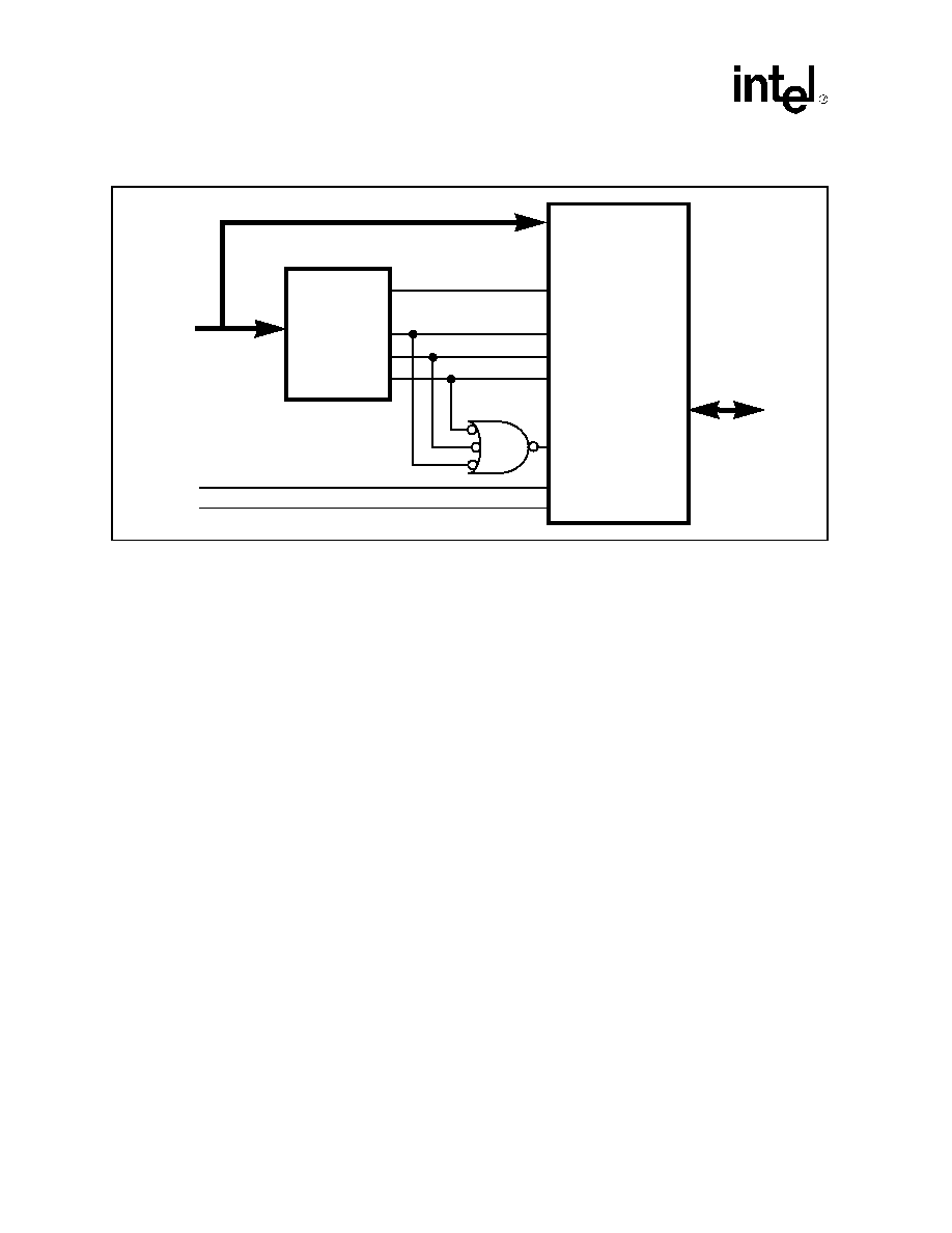
CD1400 -- UXART Serial/Parallel Controller
34
Datasheet
At the time the CD1400 is ready to post the service request, it copies the upper five bits of the
LIVR into the appropriate Vector Register (RIVR, TIVR, MIVR) and then places the request type
vector in the lower three bits. The table below shows the assignment of the request type bits.
For transmit and modem service acknowledge cycles, the data in the lower three bits will be
redundant to the host, since this information is known because the corresponding acknowledge has
taken place. However, these bits will be important for a receive data service acknowledge because
they provide an indication of whether the request is for Good Data
or exception data.
The value contained in the upper five bits of the LIVR can be used for a number of purposes. The
primary purpose of the LIVR is to source a software vector that can be used by the host system as
an index for an interrupt dispatch table. However, systems that cannot use this or do not require it
can use these bits for any purpose. In multiple-CD1400 daisy-chained designs, a logical value to
place in these bits is a chip identification number. This is discussed in more detail in the daisy-
chaining description in
"Service Requests and Multiple CD1400s" on page 37
. In a single-CD1400
design or one that does not use daisy-chaining (unique address range for each device) and does not
need the value in the LIVR as a vector for hardware interrupt response, a convenient use for these
bits is channel encoding. Since each channel has its own LIVR, these five bits can have a unique
value identifying the channel. By doing this, there is no need to read the RICR, TICR or MICR to
determine the channel number; thus in a single I/O operation, the host determines both the type of
interrupt and the number of the channel requesting service. In fact, with five bits available, systems
with small numbers of CD1400s can encode both the channel number and chip identification
number in the LIVR.
Once all of the above has been completed, the CD1400 is ready to be serviced for the type of
interrupt that has been acknowledged. For example, if the interrupt was for receive Good Data, the
host would read the RDCR to determine the number of characters available in the receive FIFO,
then read that many characters by successive reads from the RDSR. Other work, such as disabling
future interrupts or changing channel parameters could also be performed at this time. Once all
tasks involved in servicing the interrupt have been completed, one further operation must be
performed. In order to inform the CD1400 that the service acknowledge is complete, the host must
Figure 9. Control Signal Generation
SVCACKR*
SVCACKT*
SVCACKM*
DGRANT*
ADDRESS
DECODE
LOGIC
CD1400
HOST
ADDRESS
CS*
R/W*
DS*
HOST
I/O
CONTROL
HOST
DATA
AD[6:0]
DB[7:0]
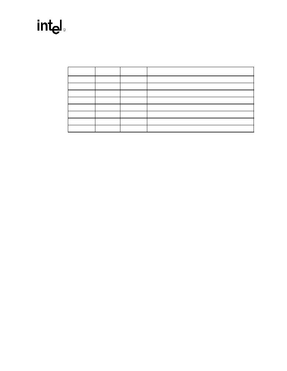
UXART Serial/Parallel Controller -- CD1400
Datasheet
35
write a dummy value to the EOSRR. The data written does not matter; any value will do. What is
important is the write operation itself. This write forces the internal context switch back to normal
Operating Mode.
Summary of Interrupt-Driven Service Requests
In summary, the actions that take place during an interrupt request/service are:
1. Host senses service request through its interrupt request input from one of the CD1400 service
request outputs.
2. Host responds by performing a read cycle that activates the appropriate SVCACK* Input Pin.
3. Host decodes the value read from the Vector Register during Step 2, making a decision on the
type of service request (if necessary).
4. Host reads (R, T, M)ICR to determine channel number.
5. Host services the request (load transmit FIFO, read receive FIFO, and so on.
6. Host writes a dummy value to the EOSRR to terminate the service routine.
7.3.1.2
Software-Activated Context Switch
It is possible -- through host manipulation of some internal registers -- to cause the context switch
without activating any of the SVCACK* Hardware Inputs. The method used is the same as that
which is used in a Poll-Mode-CD1400 design. Once the host has detected the service request
through its interrupt response circuitry, it can then follow the same procedures that a polling
method would use once it had detected an active service request. Refer to the context switching
description in the following section.
One reason a design might make use of this method is that there is limited board space available to
provide the additional hardware address decoding required to generate the three SVCACK* and
DGRANT* Control Signals. The system gains the advantage of not having to constantly check for
active service requests by polling the CD1400; it will be interrupted when a request is posted and
can then examine internal CD1400 Registers to determine the source and channel number
generating that request. If this method is chosen, the three SVCACK* and DGRANT* Input Pins
should be tied inactive (logic `1') to prevent false activation of a service acknowledge cycle due to
noise. They should be terminated with a resistor, not hard-wired to VCC.
Bit 2
Bit 1
Bit 0
Request Type
0
0
0
Not used
0
0
1
Group 1: Modem signal change service request
0
1
0
Group 2: Transmit data service request
0
1
1
Group 3: Received Good Data service request
1
0
0
Not used
1
0
1
Not used
1
1
0
Not used
1
1
1
Group 3: Received exception data service request

CD1400 -- UXART Serial/Parallel Controller
36
Datasheet
7.3.2
Polling
In Poll Mode, the hosts periodically checks the CD1400 to see if there are any active service
requests. If it detects any, it proceeds to service them through a software-driven technique. There
are several registers within the CD1400 provided specifically to facilitate Poll Mode service
request detection and acknowledgment. These are the SVRR, RIR, TIR, MIR, RIVR, TIVR and
MIVR.
"Detailed Register Descriptions" on page 88
provides detailed bit definitions for these
registers.
The SVRR (Service Request Register) is the Master Service Request Register. The least-significant
three bits (Bits 2:0, SRM, SRT, and SRR) reflect the inverse of the state of the three Service
Request Output Pins (SVCREQM*, SVCREQT* and SVCREQR*). For example, if Bit 0 (SRR) is
a `one', it indicates there is an active receive data service request pending, and that the
SVCREQR* Output Pin is active (low). Thus, with a single read, the host can determine if the
CD1400 needs any service and, if so, which ones are active.
Each service request type has an Interrupt Request Register; RIR for receive, TIR for transmit and
MIR for modem. These are special-purpose registers that are used with the CAR to force the
context switch and start a service acknowledge procedure. When a service request of a particular
type is pending, the corresponding Interrupt Request Register is set by the MPU with the
appropriate data to cause the context switch to the requested type and the requesting channel. When
the host is ready to service the request, it reads the contents of the Request Register and copies it
into the CAR. The action of writing this value into the CAR forces the context switch, and the
CD1400 is ready to be serviced. This is the same result as if a service acknowledge cycle had been
performed with the SVCACK* Pin. Each of the Interrupt Request Registers provides the channel
number that is requesting service in the least significant two bits. The most-significant three bits
provide status and control over internal interrupt sequencing. The middle three bits contain a code
that is used by the MPU at the end of a hardware service acknowledge cycles (write to the EOSRR)
to tell it which type of acknowledge cycle is ending. Each of the three registers has a unique code in
these three bits that select the proper service acknowledge type; however, they are meaningless in
Poll Mode operation.
At the end of a service request operation, the host must inform the CD1400 that the request has
been satisfied and take it out of the service request context. This is done by writing the value that
was in the Interrupt Request Register back into it after first clearing the upper two bits.
As with the hardware-driven request/acknowledge procedure, the virtual registers should only be
accessed after the context switch has been made. Their contents are undefined until this time.
Summary of Poll Mode Service Requests
To summarize, the major steps involved in a Poll Mode service request/service acknowledge
sequence are:
1. Host scans the SVRR periodically, checking the three least-significant bits. If any of them are
true (`1'), a service request is active.
2. Depending on which of the service request bits is active, read the appropriate Interrupt
Request Register (RIR, TIR or MIR) and copy the contents into the CAR.
3. Perform service routine.
4. Write the original contents of the interrupt request register back with the most-significant two
bits cleared.

UXART Serial/Parallel Controller -- CD1400
Datasheet
37
7.3.3
Service Requests and Multiple CD1400s
Multiple CD1400s can be combined to form systems with more than four channels. There are a
number of ways that two or more can be connected, but one way provides a more efficient service
request/service acknowledge sequence by allowing the CD1400s to arbitrate between themselves.
This mode only works if hardware-activated service acknowledges are being utilized.
The CD1400 provides a means of `daisy-chaining' the service request and service
acknowledgments of two or more devices together. This allows them to arbitrate and set priorities
between themselves regarding which may post a particular type of service request. This is the Fair
Share interrupt scheme.
Figure 10 on page 38
shows the way that two CD1400s would be
connected to enable the Fair Share function.
The open-drain request outputs of the two CD1400s (SVCREQR*, SVCREQT* and SVCREQM*)
are wire OR'ed together to form one request for each type. This allows each to monitor the state of
the others' outputs. Each of the Service Acknowledge Inputs (SVCACKR*, SVCACKT* and
SVCACKM*) is also connected together to form one acknowledge of each type. The DGRANT*
Input of the first CD1400 is connected to the logical OR of all three SVCACK* Inputs; the
DPASS* Output of the first CD1400 drives the DGRANT* Input of the second.
Before a request for service of a particular type is posted, the MPU checks the current state of the
`fair bit' of the internal interrupt register for that type. If it is inactive, indicating that it is fair to
post an interrupt of that type, a request can be posted; otherwise, it will wait. This guarantees that
each CD1400 will have an opportunity to have this request type serviced when needed. When the
host acknowledges the request, both CD1400s will receive the acknowledge through the
SVCACK* Input. However, only the first will receive the DGRANT*. If it has an active request of
this type pending, it will take the acknowledge and drive its Vector Register (RIVR, TIVR, MIVR)
onto the data bus.
If it does not have a request pending, it will pass the DGRANT* Input to the second CD1400
through the DPASS* Output. Assuming that the second has an active request pending, it will take
the acknowledge and drive its Vector Register onto the data bus.
As mentioned earlier, the upper five bits of the LIVR will reflect whatever the host loaded into
them during its initialization of the CD1400s. These bits must be used as a unique chip
identification number so the host will know which CD1400 responded to the service acknowledge.
These five bits could be set to binary zero in the LIVR of the first CD1400, and to binary 1 in the
second. The host can easily test the bit to determine which device responded. Some examples of
host service acknowledge software routines that show one way of performing this task are provided
in
"Programming" on page 71
.
Caution:
If neither CD1400 has a pending request, the DGRANT* will be passed by the second and neither
will respond, thus causing the cycle to hang. The only time this could happen would be due to an
error condition outside the CD1400s that caused the host to respond to a request that was not made.
A mechanism should be provided to terminate or abort the cycle if this error should occur. This can
be accomplished with time-out circuitry or the DPASS* output of the second CD1400 can activate
an abort condition. Other devices may share the daisy-chain mechanism and could be connected to
the DPASS* output of the second (or whichever is last) CD1400 in the chain. The actual
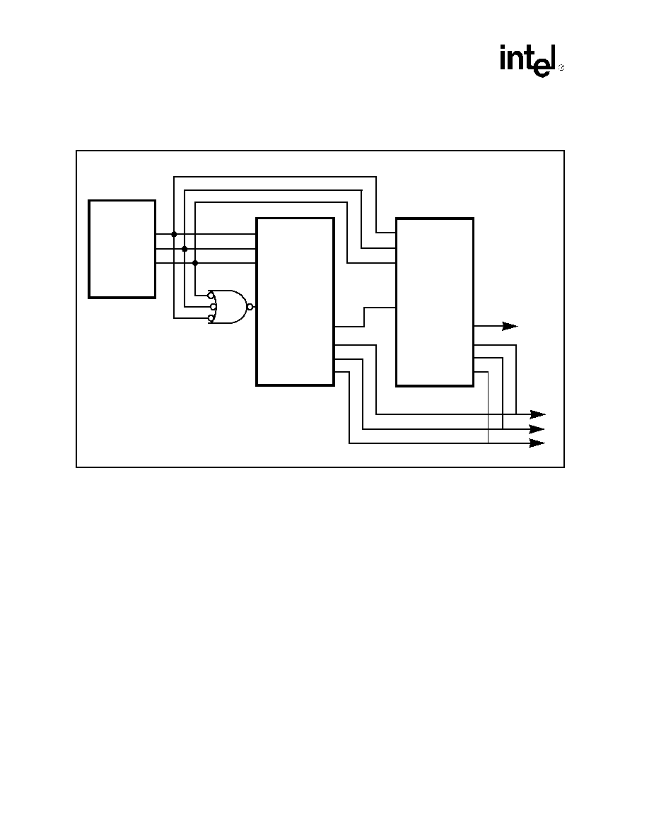
CD1400 -- UXART Serial/Parallel Controller
38
Datasheet
implementation is system-dependent, but it is important to provide some way for the host to know
that the cycle did not complete normally if no device exists at the end of the chain.
7.4
Serial Data Reception and Transmission
The CD1400 has four channels, each with a receiver and a transmitter. Although a receiver and a
transmitter pair are associated with each channel, in many respects they operate independently,
sharing only parameter settings regarding character format such as length, parity type, if any, and
number of stop bits. Each receiver and transmitter has its own baud-rate generation function,
allowing a channel to send at one rate and receive at another. Shared and independent parameters
are shown in the diagram below:
Figure 10. CD1400 Daisy-Chain Connections
DPASS*
SVCACKR*
SVCACKT*
SVCACKM*
DGRANT*
ADDRESS
DECODE
LOGIC
DPASS*
SVCACKR*
SVCACKT*
SVCACKM*
DGRANT*
SVCREQR*
SVCREQT*
SVCREQM*
SVCREQR*
SVCREQT*
SVCREQM*
CYCLE
ERROR
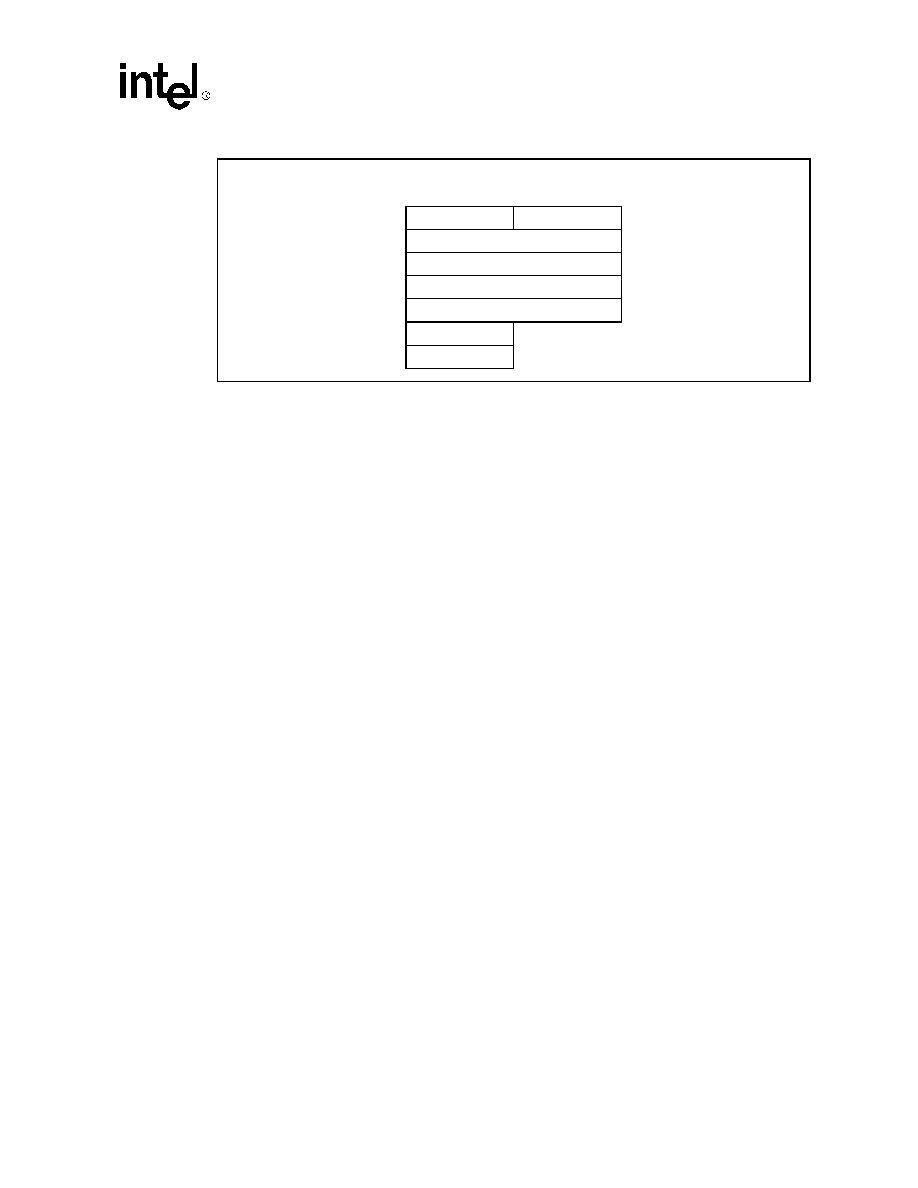
UXART Serial/Parallel Controller -- CD1400
Datasheet
39
Channel service requirements, such as an empty transmit FIFO, are indicated to the host by one of
three service request indicators: one for all receivers, one for all transmitters and one for all modem
signal changes. The internal processor (MPU) scans each channel sequentially for service needs,
posting a request when it detects a particular type. It continues the Fair Share scheme used in the
external daisy-chain configuration by not allowing a channel to post another request of one type
until all other channels have posted their requests of that type, if any. For example, if Channel 0 is
currently being serviced for a transmit request and Channel 3 has one pending, the request from
Channel 3 will be posted before Channel 0 is able to make another request for transmit service.
Each receiver and transmitter has a 12-character FIFO. The receiver has two additional character
holding locations, the Receive Character Holding Register and the Receiver Shift Register. The
transmitter also has two additional locations, the Transmitter Holding Register and Transmitter
Shift Register. The receive FIFO has a programmable threshold that sets the level at which a
service request will be posted. When data reaches this `high water' mark, a request will be made of
the host to empty the FIFO. More details on this are provided in the following section. Receive
FIFOs also have a programmable threshold that, when reached, can cause the DTR Output to be
deasserted (see the flow-control description).
In the asynchronous serial data protocol, a message consists of one `character', made up of bits,
either high or low, representing a one or zero value. A character can be made up of from five to
eight bits, plus an optional parity bit bracketed by a Start Bit and at least one Stop Bit. Each bit has
a time duration that sets the data transmission rate, or baud rate. The Start Bit indicates the
beginning of a character bit stream and is indicated by a transition from a logic `1' to a logic `0'
(mark to space) on the transmission media. The Start Bit lasts one `bit time' and is immediately
followed by the Data Bits (5 to 8), the parity, if any, and the Stop Bit(s).
As previously discussed, the CD1400 incorporates special hardware to receive and transmit each
bit. These are the `bit engines'. They perform all timing associated with sending or receiving one
serial data bit. A bit engine behaves differently depending on whether it is sending or receiving.
When a complete bit has been received, the bit engine interrupts the MPU so that it can handle the
bit on the character level. This usually entails its addition to the character being assembled. For
transmitting, a transmit-bit-engine interrupt causes the MPU to give it the next bit to be
transmitted. The bit-engine interrupt happens at the end of a bit time, which has been timed by the
engine, thus removing that duty from the MPU.
Receiver
Transmitter
Baud Rate
Baud Rate
Parity
Character Length
Stop Bits
FIFO Thresh
Prescale Period Register
Rx Time-out

CD1400 -- UXART Serial/Parallel Controller
40
Datasheet
7.4.1
Receiver Operation
Each channel can be programmed to receive characters with several different parameters, such as
character length, parity, number of stop bits, FIFO threshold and baud rate. Each receiver is
independent of any other receiver. It may also be set to a different baud rate from its corresponding
transmitter.
Before valid data can be received, the host must set up each channel by programming the desired
operational parameters in the Channel Option Registers (COR1-COR5) and the Baud Rate
Generator Registers (Receiver Clock Option Register and the Receiver Baud Rate Period Register
-- RCOR and RBPR). Once these are set, the channel is enabled by issuing the receiver enable
command through the CCR and enabling service requests in the Service Request Enable Register
(SRER).
Once a receiver is enabled, its bit engine begins scanning the RxD Input for a valid Start Bit. It
does this by detecting a falling-edge transition on the input. When the transition is detected, the bit
engine delays until the middle of the programmed bit time and checks the input again. If the input
is still low, then the start bit is considered valid and character assembly begins. At each subsequent
full bit time, the input is checked and its level recorded as the value of the next bit. If, at the center
of the bit time, the RxD Input has returned to a mark state, then the Start Bit is considered invalid
and the bit engine goes back to the Start Bit Detect Mode. Following a valid Start Bit, the bit
engine begins receiving data bits. At the end of the programmed number of bits, following bits are
checked for parity (if enabled) and a valid Stop Bit. A valid Stop Bit is defined as a mark or logic
`1' on the input.
If a valid Stop Bit is not detected, a framing error will be noted for the character. After a properly
assembled (no framing error) character has been received, it is checked for several special
conditions, and the overflow condition before it is placed in the receive FIFO. (See
"Transmit
Special Character Processing" on page 56
on special character handling and
"Flow Control" on
page 45
.)
If no errors or special character processing are required, the character is considered Good Data and
placed directly in the FIFO. If errors exist, it is placed in the FIFO as `exception' data along with
status indicating the type of error. As each good character is placed in the FIFO, the Receive Data
Count Register (RDCR) is updated to reflect the number of good characters currently in the FIFO.
The receive FIFO has a programmable threshold that determines the level at which the CD1400
will request receive data service. This level is programmed through the RxTh3-RxTh0 Bits in
Channel Option Register 3. The host may place the threshold at any number of characters from 1 to
12. Note that this only sets the level at which the CD1400 will post a service request, not the depth
of the FIFO. When the host responds to a receive Good Data service request, it may read any
number of characters out of the FIFO, from zero up to the number indicated in the RDCR before
exiting the service routine. If the number read is zero, the CD1400 will post another request for
service almost immediately. If the number of characters read is less than the number indicated by
the RDCR but enough such that the number in the FIFO falls below the threshold, a new request
will not be made until the threshold is once again exceeded. The term `almost immediately' is used
above because, since the MPU scans the channels in a `round-robin' fashion, another channel may
post a receive service request before this channel again has the opportunity.
7.4.2
Receiver Timer Operations
Also associated with each receiver FIFO is a timer whose duration is set by the Receive Time-out
Period Register (RTPR). This timer provides two services in relation to receive FIFO operation: a
time-out to prevent `stale' data in the FIFO and a time-out after the last character is taken out of the

UXART Serial/Parallel Controller -- CD1400
Datasheet
41
FIFO. The first type, Type 1, will occur if the receive FIFO does not reach the set threshold before
the programmed time period expires and the second, Type 2, will occur if the timer expires and no
new data has been placed in the FIFO after the last character was removed; this is called the No
New Data Time-out (NNDT) service request.
The timer is driven by the prescaled clock generated by the Prescale Period Register (PPR) in the
global register set. The timer is loaded with the value contained in the RTPR each time a character
is placed in the receive FIFO or when the last character is removed from the FIFO. Each `tick' of
the prescaler decrements the timer. If the timer reaches zero and receiver interrupts are enabled, the
MPU will generate a receive data service request for one of the two time-out conditions, depending
on which is valid.
Type 1:
If there are characters in the FIFO but the threshold level has not been reached, a Good Data
service request will be posted when the timer expires. This function is provided to prevent data
from remaining in the FIFO for long (potentially infinite) periods of time because the remote did
not send enough data to fill the FIFO to the threshold level. This time-out cannot be disabled.
Type 2:
If there is no data in the FIFO when the timer expires and the No New Data Time-out (NNDT)
service request is enabled in the SRER, a receive exception service request will be posted with
status indicating the time-out condition. This time-out is optional, and is provided so that host
driver software can detect the possible end of a block of data and allows its buffers to be flushed to
the higher, operating system level. The NNDT will be posted only on the first occurrence of a time-
out after the FIFO becomes empty. Also note that the NNDT timer is not started if the last character
removed from the FIFO was an exception character, such as a break or parity error.
The flow chart in
Figure 11 on page 44
shows the timer process evaluation performed by the MPU
when the timer reaches zero.
7.4.3
Receive Exceptions
Several conditions can cause the CD1400 to evoke the receive exception service request. If an
exception condition occurs, two bytes are placed in the receive FIFO. The first is the status
indicating the type of error and the second is the data itself.
Exception data is given to the host one event at a time. That is, there will be a separate service
request for each character that is received with some special condition. If, when an exception
condition occurs, the receive FIFO has Good Data in it, a Good Data receive service request will be
posted immediately upon receipt of the bad data, regardless of the number of characters in the
FIFO and the programmed threshold. This allows the host to remove the data in the FIFO ahead of
the exception data so that the CD1400 can post the service request for the error condition. Once the
host terminates the service acknowledge procedure for the Good Data, a new service request will
be posted for the exception data.
When the host acknowledges the receive exception service request, it reads the Receive Data/
Status Register (RDSR) first to get the status and second to get the data. Reading the data is
optional: if the host does not read the FIFO twice during the service routine, the CD1400 will
update its internal FIFO pointers appropriately and discard the second byte. (Actually, the host

CD1400 -- UXART Serial/Parallel Controller
42
Datasheet
need not read any data from the FIFO during an exception service acknowledge ≠ the FIFO
pointers will update correctly at the end of the service routine, discarding both the status and the
data. Thus, the host must read at least the status, or it will be lost forever.)
Another special case of the exception data handling is for received-line-break conditions. A line
break is a character with zero data and no parity or Stop Bit. In this case, a null (zero) character is
placed in the FIFO with the break condition indicated in the accompanying status and a receive
exception service request will be posted. However, regardless of the length of the break, only one
character will be placed in the FIFO. If the `end-of-break' option is enabled, another null character
is placed in the FIFO with status indicating the end-of-break condition, once it is detected in the
receive data stream. This option is enabled by the EBD Bit (Bit 2) of COR5 -- see
"Channel
Registers" on page 99
for details. Resumption of normal character reception will cause new data to
again be placed in the FIFO.
Refer to the register definitions in
"Detailed Register Descriptions" on page 88
for a description of
the status bits in the RDSR.
7.4.4
Transmitter Operation
Each of the four channels on the CD1400 are capable of transmitting characters with a number of
programmable characteristics such as length, parity and baud rate. The channels operate
independently and settings in one have no effect on the operation of another.
After being reset, from either hardware (RESET* Input Pin) or software (through the master reset
command in the CCR), all transmitters are disabled with the TxD Output held at a logic '1'
condition. This is the off, or mark, condition of the asynchronous protocol. Before any operation of
the transmitter can begin, the host must program the appropriate parameters in the Channel Option
Registers (COR), the Clock Option Register (TCOR) and Transmit Baud Rate Period Register
(TBPR). Once these registers are set, the channel is enabled by issuing a transmit enable command
through the CCR and enabling service requests by setting the appropriate transmit enable request
bit(s) in the Service Request Enable Register (SRER). The channel will immediately post a
transmit service request since its FIFO is empty. The host responds to the request by loading up to
12 characters into the transmit FIFO through the Transmit Data Register (TDR) after it places the
CD1400 in the Service Request Acknowledge Mode (see description of service request/service
acknowledge procedures in
"Poll Mode Examples" on page 75
). The transmitter does not begin
transmitting the characters until the host terminates the service routine and writes the EOSRR.
Transmission begins by sending a Start Bit (logic '0') followed by five to eight data bits (depending
on the programmed value), least-significant bit first. The last data bit is followed by the appropriate
parity bit, if enabled, and a minimum of one stop bit. All bit transmission is handled by the transmit
bit engine with the MPU giving it each bit as it is required. If there are still characters in the FIFO,
the next one will be transmitted immediately after the last stop bit of the previous character. This
process continues until all characters in the FIFO have been transmitted. The CD1400 will then
post a service request for more data.
There are actually 14 transmit character holding locations for each channel: 12 in the FIFO, one in
the Transmitter Holding Register, and one in the Transmitter Shift Register itself. The CD1400 can
be programmed, on a per-channel basis, to request transmit data when one of two conditions exist:
when the last character in the FIFO is transferred to the Holding Register or when the last data bit
of the last character is shifted out of the Transmitter Shift Register. The first option allows the host
two character transmit times in which to reload the FIFO and prevent a transmit data underrun.
This is the normal mode of operation. The second mode can be used to make sure the transmitter is
empty before reconfiguring the channel. It is likely that the transmitter will underrun if the second
option is chosen unless the host is sufficiently fast enough to respond to a transmit service request
and reload the FIFO during the transmission of the stop bit(s) of the last character. If the transmitter

UXART Serial/Parallel Controller -- CD1400
Datasheet
43
underruns, it will continue to send stop bits (mark) until more data is placed in the FIFO. Normally,
when a string of characters greater than 12 is being transmitted, host software will program the
CD1400 transmitter to post a service request when the FIFO becomes empty. When the last of the
data to send has been placed in the FIFO, the service request enable is changed so that requests are
made after the last character is sent. This allows the host to know that all the data has been
transmitted before disabling a channel. If a channel is disabled, any characters other than the one
currently being transmitted will be held and the transmitter will enter the marking state. If the
channel is subsequently re-enabled, any remaining data will be transmitted.
The transmitter is capable of performing several special functions such as break generation, inter-
character delays and automatic flow control. These functions are discussed in the sections
describing special character handling (embedded transmit commands) and flow control.
7.4.5
Transmitter Timer Operations
As with the receiver, the transmitter has a timer associated with it. This timer is used to generate the
timing for the embedded transmit commands that send line breaks and inter-character delays.
Whenever the MPU detects an embedded transmit command specifying the delay command, it
loads the timer with the value contained in the parameter byte. This timer is decremented on each
`tick' of the prescaler timer (PPR) until it reaches zero. At that time, the delay is terminated unless
the next character in the FIFO is the beginning of another delay-command sequence.
CD1400 -- UXART Serial/Parallel Controller
44
Datasheet
Figure 11. FIFO Timer Processing
TIMER = 0
?
from other background
processing
background scanning
detects new character
arrived
put character in FIFO
reload timer
resume background
scanning loop
FIFO empty
?
No New Data
Time-out
Enabled
?
No New Data
internal flag
armed
?
clear NoNewData
internal flag
post receive exception
service request
resume background
scanning loop
Y
Y
Y
Y
N
N
N
N
post receive Good Data
service request

UXART Serial/Parallel Controller -- CD1400
Datasheet
45
7.5
Flow Control
In all data communications applications, data is sent from one system to another through some
protocol. Most systems have some method of buffering data for transmission and reception. In the
asynchronous protocol, there is no way, at the protocol level, to determine the length of a data
transmission; therefore, it is normally not possible to set aside a buffer area that is known to handle
the entire length of the transmission. Also, the hardware receiving the data generally has a limited
amount of buffer area, usually a FIFO, and if the host does not unload data at a fast enough pace,
the buffer or FIFO may overflow. For these reasons, two methods are provided that can be used to
stop the remote from sending data until room is once again available to receive data. This is known
as flow control. Flow control can be in-band or out-of-band. In-band flow control makes use of
special characters that can be sent to the host to stop data transmission. Out-of-band flow control
are signals outside of the serial data channel that perform the same function. These are the Request
To Send (RTS), Clear To Send (CTS) pair and the Data Set Ready (DSR) and Data Terminal Ready
(DTR) pair. The CD1400 can make use of either kind and has built-in capabilities to do so
automatically and/or semi-automatically (depending on direction and options chosen) without host
intervention (or knowledge, if desired).
7.5.1
In-Band Flow Control
As mentioned, in-band flow control is implemented by special characters that are imbedded in the
serial data stream, one to request that transmission stop and one to request resumption. The
characters chosen can be any characters although conventionally the XON or DC1 (x'11) and
XOFF or DC3 (x'13) characters are used if the ASCII character set is being used. The XOFF value
designates the character that is to be used to stop data transmission and the XON character
determines the character that is to be used to resume transmission. Whether or not the ASCII XON
and XOFF Characters are used, the CD1400 allows the two characters to be set to any value that is
appropriate to the system design by the value programmed in Special Character Registers 1 and 2
(SCHR1 and SCHR2). SCHR1 defines the XON Character and SCHR2 defines the XOFF
Character.
7.5.1.1
Receiver In-Band Flow Control
When the host senses a need to flow control a sender, due to its receive buffer filling too fast to
service, it can request that remote stop transmission by sending an XOFF character through the
transmitter. This is accomplished by issuing a Send Special Character 2 command through the
Channel Command Register (CCR). The CD1400 will then transmit whatever character is
programmed in SCHR2. As discussed earlier, the send special character command is preemptive to
data currently in the transmit FIFO, and thus the XOFF character will be transmitted after the
currently transmitting character and the character in the Transmitter Holding Register have been
sent, a maximum delay of two character times. When the host is again ready to start receiving
characters, it sends an XON Character, also through a send special character command. This time,
the CD1400 is issued the command to send whatever is programmed in SCHR1. Send special
character commands will override the remotes' flow-controlling of the CD1400; in other words,
even if the CD1400 transmitter has been shut off by the remote, it can still send flow control
characters.
The current state of the flow control condition is always made available to the host through the
Channel Control Status Register (CCSR). In addition to the enabled/disabled status of the receiver
and transmitter, the CCSR displays the flow control status. Two bits in the CCSR pertain to
receiver flow control, RxFloff and RxFlon. Whenever the host issues the send Special Character 2
(send XOFF), the CD1400 sets the RxFloff Bit, indicating that it has requested the remote to stop
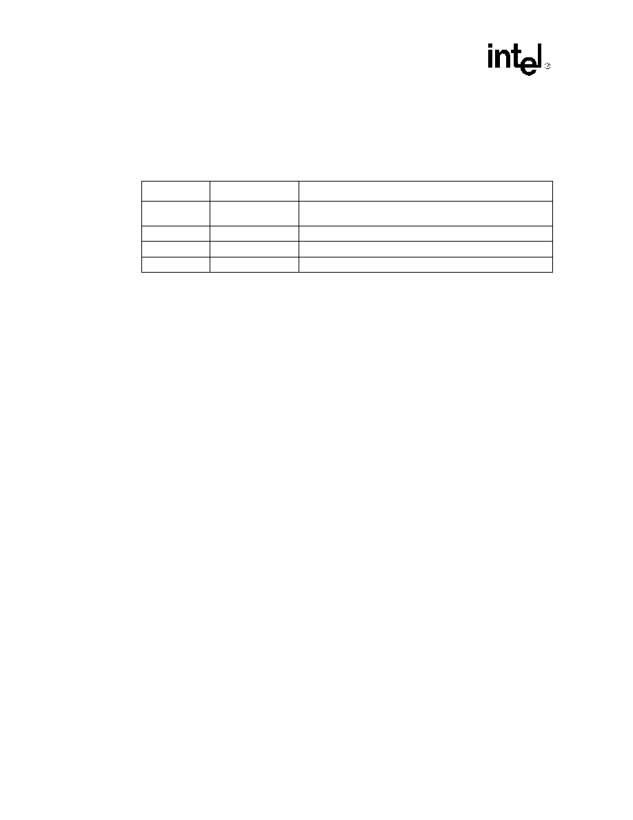
CD1400 -- UXART Serial/Parallel Controller
46
Datasheet
transmission. When the host issues the send Special Character 1 (send XON) command, the
RxFlon Bit is set and RxFloff is reset. RxFlon remains set until the first character is received after
the XON was transmitted. The table below shows the bit encoding for RxFloff and RxFlon.
The RxFloff/RxFlon Bits are cleared whenever the receiver is disabled or enabled, regardless of the
state of flow control when the disable/enable occurred.
Note:
Regardless of the current state of RxFloff, the
CD1400
continues to receive characters. If the
remote ignores or is slow to respond to the XOFF Character, there is the possibility of overruns.
7.5.1.2
Transmitter In-Band Flow Control
The CD1400 has the ability to automatically flow control its own transmitter when it receives the
XON and XOFF Characters, as programmed in SCHR1 and SCHR2. Control Bits in Channel
Option Registers 2 and 3 (COR2 and COR3) enable or disable various aspects of the automatic
flow control.
In order for flow control characters to be acted upon, special character detection must be enabled
through Bit 4 (Special Character Detect 1 and 2 -- SCD12) of COR3 and Bit 6 (TxIBE) of COR2.
When these bits are set, the CD1400 will scan received characters for a match with one of the
special characters programmed in SCHR1-SCHR2. If enabled, and it has received a character
matching the contents of SCHR2 (the XOFF Character), the CD1400 will then check to see if
automatic transmit in-band flow control is enabled through Bit 6 of COR2. If this function is
enabled, the CD1400 will cease transmission after the currently transmitting character and the
character in the transmitter holding register, if any. If enabled, the CD1400 will also attempt to
match against erroneous characters. This function is enabled through the CMOE Bit in COR5.
One other Control Bit in COR2 is involved in flow control activities. This is Bit 7, the Implied
XON Mode, IXM. This bit determines what character will restart transmission after an automatic
flow control has caused it to stop. If Bit 7 is a zero, only a programmed XON Character (SCHR1)
will restart the transmitter; all other characters will be received and placed in the FIFO normally. If
IXM is set, any character received will restart data transmission.
As with receiver flow control, the host can always determine the current state of the transmitter
through two bits in the CCSR: TXFloff and TxFlon. When automatic in-band flow control is
enabled and the CD1400 receives and XOFF character, it sets TxFloff. When an XON character is
received, TxFlon is set. Once transmission actually resumes, TxFlon is cleared. The encoding is
shown in the table below.
The TxFloff/TxFlon Bits are cleared whenever the transmitter is disabled or enabled, regardless of
the state of flow control when the disable/enable occurred. This feature can be used to force
resumption of transmission regardless of remote initiated flow control.
RxFloff
RxFlon
Encoded Status
0
0
Transmission has resumed, receiver has been enabled/disabled or
receiver is in default reset state
0
1
XON has been sent, transmission not yet restarted
1
0
XOFF has been sent
1
1
Not Used
UXART Serial/Parallel Controller -- CD1400
Datasheet
47
There is one final aspect of automatic in-band flow control: Flow Control Transparency (FCT)
which is enabled/disabled by Bit 5 in COR3. FCT determines whether or not remote flow control
will be transparent to the host. If this bit is not set, in addition to stopping transmission when an
XOFF is received, the CD1400 will place the received XOFF Character in the receive FIFO and
inform the host of the reception through a receive exception service request. When the XON
Character is received, it too will be given to the host through an exception service request as well as
restarting data transmission. If FCT is enabled, received flow control characters will control
transmission but they will be discarded rather than be placed in the FIFO. If the host system
software doesn't need to be informed when its transmit data has been stopped, this bit can be set to
reduce the number of service requests that must be handled.
The table below summarizes the Control Bits in the Channel Option Registers that enable the
various modes of in-band flow control.
7.5.2
Out-of-Band Flow Control
Flow control can also be accomplished through the modem handshake signal pairs RTS/CTS and
DSR/DTR. These are called out-of-band flow control because they are external to the data channel.
The CD1400 can be programmed to automatically respond to and generate out-of-band flow
control through these signals.
7.5.2.1
Receiver Out-of-Band Flow Control
Along with the receiver FIFO threshold that sets the level at which the CD1400 will post a service
request, another threshold can be set that determines when it will automatically assert/deassert the
DTR* Output if so enabled. This is the DTR threshold and is enabled through the DTRth3-DTRth0
Bits in Modem Change Option Register 1 (MCOR1). The level can be set for any number of
characters from 0 to 12, with a threshold of 0 disabling the function. If the function and the receiver
are enabled, the CD1400 will automatically assert the DTR* Output whenever the number of
characters in the receive FIFO is less than the programmed number. Once the level reaches the
threshold, DTR* will be deasserted. DTR* will be held in the deasserted state until the host
removes enough characters from the FIFO to lower the level below the threshold.
In order for the receiver to operate properly, the DTR threshold must be set to a value equal to or
higher than the receiver service request threshold. If the levels were reversed, normal character
reception could not be completed because DTR* would always be deasserted before the receive
FIFO threshold is reached, thus the host would not get a receive data service request until the
receive FIFO time-out is reached. A serial data transmission performance limitation would result.
The DTR* Output may also be controlled manually through Bit 1 of Modem Signal Value Register
2 (MSVR2). Setting this bit to a `1' will assert the DTR* Output.
TxFloff
TxFlon
Encoded Status
0
0
Transmission has resumed, transmitter has been
enabled/disabled or transmitter is in default reset state
0
1
XON has been received, transmission not yet restarted
1
0
XOFF has been received, transmission has stopped
1
1
Not Used
CD1400 -- UXART Serial/Parallel Controller
48
Datasheet
The DSR* Input can also be used to flow-control the receiver. If this mode is enabled through Bit 0
of COR2 (DSR Automatic Enable -- DsrAE), and characters received while DSR* is deasserted
will be discarded.
7.5.2.2
Transmitter Out-of-Band Flow Control
Transmitter out-of-band flow control is implemented with three Modem Control Signals: the RTS*
Output and the CTS* and DSR* Inputs. The RTS* Output can be programmed to automatically be
asserted whenever there is data in the transmit FIFO and the transmitter is cleared to send. CTS*
and DSR* can be enabled to automatically control the transmitter.
RTS Automatic Output (RtsAO) is enabled through Bit 2 in COR2. If this bit is set, the CD1400
will automatically assert the RTS* Output when there is data in the FIFO to send. When the data
has been sent and the FIFO is empty, RTS* will be deasserted until the host inserts more data. If
RtsAO is not set, the host software must control the RTS* output manually through Modem Signal
Value Register 1 (MSVR1) if required by the remote.
The CTS* Input can also be monitored by the CD1400 and used as a transmitter enable. The
function is enabled by setting Bit 1 (CTS Automatic Enable -- CtsAE) of COR2. If the function is
enabled, character transmission will occur only when the CTS* Input Signal is asserted. If the
signal is deasserted during active transmission, the current character plus the character in the
Transmitter Holding Register, if any, will be transmitted and then transmission will cease. Thus, a
minimum of one and a maximum of two characters may be transmitted after the control signal is
deasserted. Transmission will resume when the signal(s) are reasserted.
The send special character command does not, however, sample the CTS* Input. If the host
chooses to send one of the special characters, the character will be transmitted regardless of the
state of this input. In most cases, this is desirable so that the host can `flow-control' a remote even
if the host is itself flow-controlled. If the state of CTS* is important, it should be tested through
MSVR1 before the special character send command is issued.
7.5.3
Modem Signals and General-Purpose I/O
Each channel of the CD1400 has four pins that can be used either as modem-control or general-
purpose input/output pins. The modem signal names assigned to these four pins have been chosen
to provide an easy reference for systems designers. In fact, they are all simply general purpose
inputs and outputs (if automatic out-of-band flow-control is not used) that can be individually
controlled through the modem signal value register(s). Since they are general purpose, system
designers may choose to connect the pins in any way that suits the application.
However, when the system software design chooses to make use of the automatic out-of-band flow
control with the pins, then the signal naming convention no longer holds true in some cases,
depending on whether the device is used as DCE or DTE. In this case, it is best to think of the pins
in terms of their actual uses within the CD1400 and connect them accordingly, without regard to
Bit Name
Register
Function
SCD12
COR3
Enables recognition of Special Characters 1 and
2
FCT
COR3
Enables transparent flow control
TxIBE
COR2
Enables automatic transmitter in-band flow
control
IXM
COR2
Enables implied XON Mode
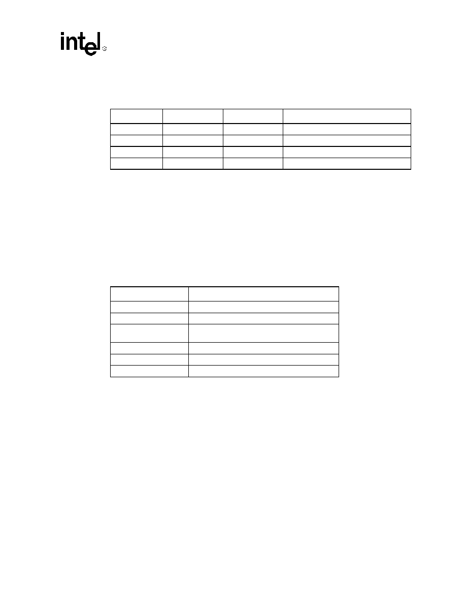
UXART Serial/Parallel Controller -- CD1400
Datasheet
49
their names. The RTS* and CTS* Pins are associated with the transmitter and the DTR* and DSR*
Pins are associated with the receiver. The table below shows recommended signal hook-up if
automatic, out-of-band flow control is desired.
For example, if the CD1400 is designed to be a DCE and automatic out-of-band flow control is
desired, the pin labeled DTR should be connected to remote CTS input. If the CD1400 is to be used
as the DTE side, then the CD1400 CTS output would be connected to the remote CTS input.
Note that if automatic out-of-band flow control is implemented, the activity of DTR and DSR Pins
do not implement the function assigned to those signal names by the signalling conventions of the
CCITT and other standards organization. These names would only apply to these pins if they are
under program control and not under automatic CD1400 control. In fact, the `DTR' function, as
defined, enables the modem to go on- and off-line, depending on the state of the pin. If automatic
control is used, then DTR would go inactive when the receive FIFO reached the programmed
threshold thus causing the modem to drop the connection (carrier) to the remote, which would not
be the correct function.
Modem pins are implemented as I/O ports accessible by either the CD1400 processor or the host.
The modem pins are not connected directly to the transmit or receive hardware. When a user
programs out-of-band modem functions to be active, the CD1400 processor will read from and
write to these pins. Specifically, when RTS* and CTS* are being used for transmit flow control,
the CD1400 processor will assert RTS* and sense CTS*, as required. Likewise, when configured
to do so, the Receive FIFO will negate DTR* when full. The host should not be allowed to re-assert
it inadvertently. The host is not `locked out' of accessing these bits; care should be taken so that
these bits are not written to, causing the system to malfunction.
The user has direct control over the RTS* and DTR* Outputs and can sense the state of CTS*,
CD*, and DSR* Inputs through the Modem Signal Value Register (MSVR). Since the host is
accessing these pins directly, there is no delay in the host's ability to detect a level change. DTR*
and CD* depend on the state of the DTRSEL input.
When the CD1400 is programmed to detect level changes and generate service requests when level
changes occur, it does so in firmware by reading the pins and comparing to a previously stored
value. This function is performed in the main timing loop of the firmware; the maximum time
required to detect a level change under worst-case conditions is approximately 2 milliseconds.
DCE
DTE
CD1400 Pins
Out-of-Band Flow Control
CTS
DTR
Signal remote to transmit
RTS
Not implemented in this direction
RTS
RTS
Request remote permission to transmit
CTS
CTS
Enable transmitter
Modem Control Pins
Function
RTS*
Request to Send (general-purpose output).
CTS*
Clear to Send (general-purpose input).
DTR*
Data Terminal Ready (carrier detect/general-purpose
input/output).
DSR*
Data Set Ready (general-purpose input).
CD*
Carrier Detect (general-purpose input).
RI
Ring Indicator (general-purpose input).

CD1400 -- UXART Serial/Parallel Controller
50
Datasheet
When the CD1400 is performing this function, the modem pins are periodically sampled rather
than continuously monitored; as such they have very little sensitivity to noise, which is desirable in
data communication applications. However, in extremely noisy applications, re-read a modem line
which has caused a Modem Signal Change Service Request to verify that it has indeed changed and
is not merely malfunctioning. This will eliminate even the slight possibility of a noise pulse
causing erratic operation.
When the CD1400 is monitoring modem pins to control transmit or receive functions, it does not
rely on the previously stored value, but checks the pins at the appropriate time. Thus, there is very
little delay in this response. For example, before deciding to transmit another character, it will
examine the CTS* Pin at that time. (The CD1400 makes this decision when moving characters
from the FIFO to the Holding Register, not from the Holding Register to the Shift Register.)
Note that the logical sense of the modem bits is inverted; that is, writing a `1' to MSVR1 or
MSVR2 causes the output pin to go to nominal zero volts. Likewise, a low-voltage input will be
sensed as a `1'.
7.5.3.1
Generating Service Requests with Modem Pins
The CD1400 can generate service requests when any one of the input pins changes state. Either or
both edges may be detected by setting bits in the two Modem Change Option Registers (MCOR1
and MCOR2). For each pin, the user can individually enable on-to-off or off-to-on transition
detection of the inputs. When the CD1400 detects such a transition, it sets the corresponding bit in
the Modem Change Register. If the corresponding bit in the channel's Interrupt Enable Register is
set, the CD1400 will assert its IREQ1* Output. The user must clear the Modem Change Register
during the service request service routine before writing to the EOIR.
The CD1400 performs this task by reading the modem input signals and comparing the current
value with the value read in the last pass through the outer scanning loop. Because this is the
lowest-priority event in the CD1400 scanning loop, changes may not be detected unless they are
several hundred microseconds long. Modem Input Pins can be used for purposes such as detecting
the closing of a switch. However, the relatively slow speed of response should be taken into
account when using Modem Input Pins for this purpose. The CD1400 does not latch the Modem
Input Signals.
7.5.3.2
Using Modem Pins as General-Purpose I/O
Since the modem pins can be directly accessed by the host, they can be used as general-purpose I/O
pins if they are not needed for flow control or modem interfacing. Simply read from and write to
them as any I/O port.
7.6
Receive Special Character Processing
The CD1400 has several means of sending special characters and ways in which it processes these
characters when it receives them. Some special characters can have fixed definitions and some can
be user-defined. The flow-chart at the end of this section defines the processing that the CD1400
performs for receive data. The chart may aid in understanding the special character handling
process.

UXART Serial/Parallel Controller -- CD1400
Datasheet
51
7.6.1
UNIX Character Processing
The CD1400 incorporates special character processing that can be of particular benefit in systems
designed to run the UNIX operating system. The processing performs some of the functions
normally handled by the `line discipline' part of a serial device driver program. The effect of this is
higher overall performance in serial communication than would otherwise be obtained because the
character manipulation takes place at the hardware level without host action. This processing
includes carriage return (CR) and new line (NL) substitution, programmable response to errored
characters (framing, parity and overrun errors), the LNext function and ISTRIP. Each of the types
of processing is optional; any, all or none of them can be enabled/disabled through control bits in
the Channel Option Registers two, four and five (see the detailed register descriptions for the
format of COR2, COR4 and COR5). This section gives detailed descriptions of each of the
functions.
If Channel 0 is programmed as a parallel channel, only the transmit special character processing
occurs, such as repeat space and carriage return and new line translation.
7.6.1.1
Line-Terminating Characters
The CD1400 can be programmed to perform automatic substitution of carriage return (CR) and
new line (NL) characters on both received and transmitted data. Received character processing has
five unique substitutions based on the value of three bits in COR4 - IGNCR, ICRNL and INLCR
(some combinations cause identical actions):
000
Do nothing ≠ function not enabled
001
Received NL changed to CR
010
Received CR changed to NL
011
Received CR change to NL and received NL changed to CR
100
Received CR discarded
101
Received CR discarded and received NL changed to CR
110
Received CR discarded
111
Received CR discarded and received NL changed to CR
7.6.1.2
Errored Character Processing
The CD1400 provides a number of ways to handle characters that are received with errors (parity,
framing and overrun errors). If none of the special processing functions are enabled, errored
characters are delivered to the host through a receive exception service request. Alternatively, these
characters can be handled in one of the following ways, as defined by the PE[2:0] Bits of COR4:
∑
Parity errors can be ignored -- the character is placed in the FIFO as Good Data and is given
to the host as any other received Good Data.
∑
An errored character can be replaced with a NULL (x'00) character in the FIFO.
∑
An errored character can be replaced in the FIFO with the three byte string x'FF - 00 -
character. If this mode is enabled and an actual good x'FF character is received, it is replaced
in the FIFO by two x'FF characters.

CD1400 -- UXART Serial/Parallel Controller
52
Datasheet
∑
An errored character can be discarded.
Received breaks are handled a little differently from other errored characters. They can be
processed, based on the settings of the IGNBRK and -BRKINT Bits in COR4, as:
∑
Reported as an errored character through a received exception service request.
∑
Replaced with a good NULL (x'00) character in the FIFO.
∑
Discarded
7.6.1.3
LNext
This function provides a means of `escaping' or ignoring any special meaning of special characters
and treats them as normal data. The escape character is defined by the value in the LNC Register. If
the CD1400 receives this character, it will put it and the next character in the FIFO without further
processing. This allows, for example, a flow-control character to be received without it actually
causing flow-control activity. LNext can be enabled to operate even on characters that are received
with errors (parity, framing, overrun), otherwise errored characters are handled normally and the
next character is not escaped.
7.6.1.4
ISTRIP
ISTRIP is a simple function that, if enabled, resets the most-significant bit (Bit 7) of all received
good characters. If the character has a parity or framing error, the ISTRIP function does nothing
and the character is given to the host through a normal receive exception service request.
7.6.2
Non-UNIX Receive Special Character Processing
In addition to the UNIX special character processing, the CD1400 provides other special character
recognition capabilities. The CD1400 has four registers that define special characters, SCHR1-
SCHR4. Two of these, SCHR1 and SCHR2 are used in flow control activities and were discussed
in the flow control section. SCHR3 and SCHR4 define two additional special characters that the
CD1400 can scan for in the receive data stream. Recognition of Special Characters 3 and 4 are
enabled by the SCD34 Bit of COR3 (Bit 6). If either of these are received, it is cause for a special
character detect (receive exception) service request. It should be noted that if automatic in-band
flow control is not enabled, SCHR1 and SCHR2 can still be used as special characters. They will
be detected and reported as receive exceptions, but will not cause any flow control activities to be
invoked.
Another special character function is the range detect function. If this mode is enabled (through the
SCDRNG bit in COR3), the CD1400 will compare all received characters against the values in
Special Character Range Low (SCRL) and Special Character Range High (SCHL). If the character
received falls between these two values (inclusive), a special character detect service request will
be posted.
The status shown in the RDSR indicates which of the special character recognition conditions were
met and that caused the receive exception service request. See the RDSR description in the register
definitions in
"Detailed Register Descriptions" on page 88
for the bit encoding.
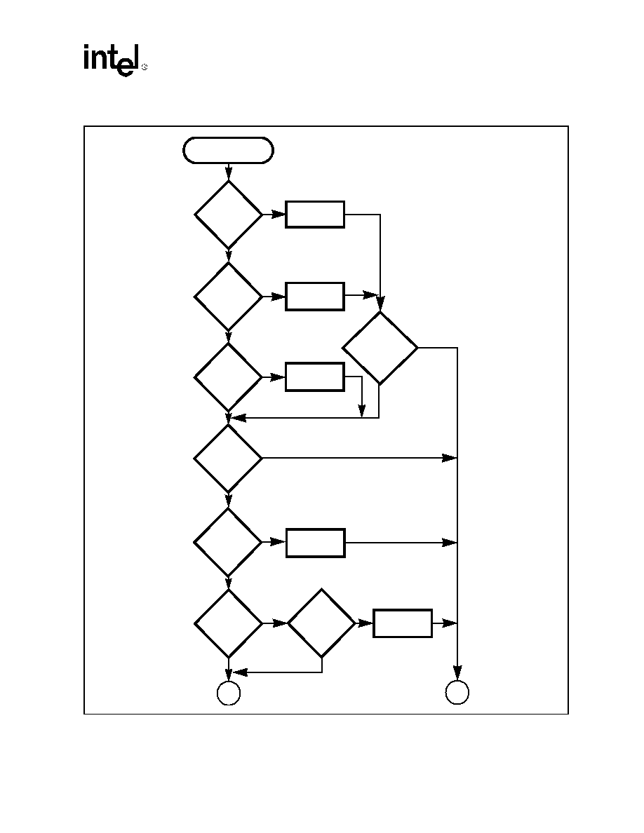
UXART Serial/Parallel Controller -- CD1400
Datasheet
53
Figure 12. CD1400 Receive Character Processing
Parity,
Framing,
Overrun
error
Character
Received
?
Set Errored
Char Flag
Set Break
Flag
Clear LNext
Flag
Set D7 = 0
Y
Y
Y
Y
Y
Y
Y
Y
N
N
N
N
N
N
N
N
A
B
Break
ISTRIP
Enabled
?
?
Char Match
on Error
Enabled
?
SCHR12
Enabled
?
LNext
flag
?
set
LNext
Mode
Enabled
?
Char
=
LNext
?
Set LNext
Flag
(Continued on next page)
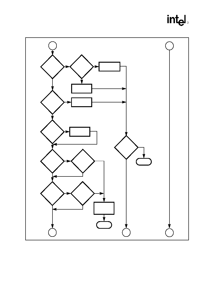
CD1400 -- UXART Serial/Parallel Controller
54
Datasheet
B
A
Implied
XON Mode
Clear Flow
Off
XOFF
Character
XON
Character
Set Flow
Off
Toggle Flow
State
XON
Character
Clear Flow
Off
Flow
Control
Transparency
Set
Done
Done
SCHR34
Enabled
SCR
Enabled
Character
In Range
Set Special
Character
Exception
Character
Match
C
D
E
?
?
?
?
?
?
?
?
?
Y
Y
Y
Y
Y
Y
Y
Y
Y
N
N
N
N
N
N
N
N
N
(Continued on next page)
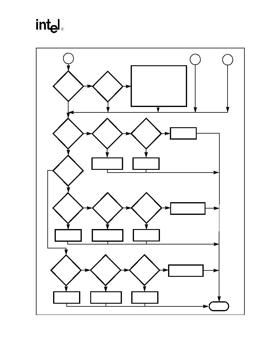
UXART Serial/Parallel Controller -- CD1400
Datasheet
55
CR/NL
Processing
Enabled
Char =
CR or NL
C
D
E
CASE:
000 - Do Nothing
001 - NL to CR
010 - CR to NL
011 - CR to NL; NL to CR
?
?
Y
Y
N
N
Parity
Error
Handling
= `100'
?
Y
N
Error Flag
Set
?
Y
N
Y
N
Char =
x'FF
?
?
N
Y
Put FF,00, char
in FIFO
Put FF, char
in FIFO
Put char
in FIFO
100 - Discard CR
101 - Discard CR; NL to CR
110 - Discard CR
111 - Discard CR; NL to CR
N
Y
N
Y
N
Parity
Error
Handling
= `011'
?
Parity
Error
Handling
= `010'
?
Parity
Error
Handling
= `001'
?
Post Exception
Service Request
Y
Y
N
Y
N
?
?
Break
Processing
Mode
= `10'
?
Post Exception
Service Request
Discard Char
Put Char
in FIFO
Put 00
in FIFO
Put 00
in FIFO
Put Char
in FIFO
N
Break
Processing
Mode
= `11'
Break
Flag
Set
Y
Done
Parity
Error Flag
Set
Parity
Discard Char

CD1400 -- UXART Serial/Parallel Controller
56
Datasheet
7.7
Transmit Special Character Processing
∑
The CD1400 also provides some special character handling on the transmit side; embedded
transmit commands and direct commands that cause transmission of predefined special
characters. A flow chart (
Figure 13 on page 59
) is included at the end of this section to help
describe the process of special character handling.
7.7.1
Line Terminating Characters
On transmit, there are four possible substitutions based on the setting of two flags in COR5 (Bits 1
and 0 -- ONLCR and OCRNL):
00
Do nothing -- function not enabled
01
Change all <CR> characters to <NL>
10
Change all <NL> characters to <CR> <NL>
11
CR characters changed to NL or NL changed to <CR> <NL>
In the last case, where both flags are set, only one of the translations will take place. In other words,
a CR that has been changed to NL will not then be changed into CRNL.
7.7.2
Embedded Transmit Commands
The CD1400 has a special feature that optionally allows specific `escape' character sequences in
the transmit data stream to be interpreted as commands. These are called Embedded Transmit
Commands (ETC) and are enabled by the ETC Bit in Channel Option Register 2. They can be used
to insert programmed time delays between characters and generate a line break on the transmit data
output.
If enabled, an ETC is detected when the two- or three-character `escape' sequence is detected in the
transmit FIFO. An escape-character sequence is made up of the special escape character followed
by the command character and an optional count for the delay period. The escape character is an
all-zero (null) character. It should not be confused with the ASCII ESC character, which is 1B hex;
for this discussion, ESC refers to the null character. Five commands are supported in the ETC
command set:
ESC ESC:
Send one ESC character. This command sequence is provided to allow the ESC character to be sent
alone. Thus, this `escapes' the escape when it is actually desired to send a null character.
ESC x'81:
Send BREAK. This causes the transmitter to enter the line-break condition for at least one
character time. Several conditions control the continuation and/or termination of the line break. If
there is no more data in the FIFO following the send break command, the break will continue
indefinitely until terminated by a stop break command. If there is an insert delay command (see the
next command) immediately following the send break command, the break duration will be set by

UXART Serial/Parallel Controller -- CD1400
Datasheet
57
the value programmed in the delay command. Any other character in the FIFO immediately
following the send break command carries an `implied' end of break condition, causing the break
to be terminated and the next character to be sent.
ESC x'82 x'xx:
Insert delay. This command will cause a delay between the previous character transmitted and the
next character to be transmitted. The hex value contained in the third byte of the sequence
determines the time of the delay based on the basic time period set by the Prescale Period Register
(PPR). The value is treated as an unsigned binary value that is loaded into an internal counter. The
counter is decremented once for each `tick' of the prescale period timer. Thus, if the PPR sets a
basic timing period of 10 ms and the value set by the command is 100 (x'64), then a delay of 1
second will be generated. Multiple insert delay commands can be placed in the FIFO if time delays
longer than that generated by a single delay period are needed.
This command is useful when a delay is required after sending a carriage return. A printer is an
example of this type of situation. Often, the carriage return causes the printer to start a print cycle
and the sending device must wait for the print to complete before sending the next line of text
(unbuffered input). Using the insert delay command allows the delay to be performed
automatically without the need for the host to time it. The delay command is placed in the FIFO
directly following the carriage return and preceding the first data for the next line. The
CD1400
will automatically execute the delay following the carriage return and then start sending characters
again.
Another useful application of the delay command is as a built-in timer that the host can use as an
interrupt source causing it to periodically check its internal buffers for data to transmit. This
assumes that the channel is not currently transmitting data. When the host services the transmit
FIFO service request after a delay time-out, as set by the delay value, it can start transmission of a
buffer if data is available or re-send the insert delay command and wait for the next service request.
This removes the necessity of the host setting an internal timer interrupt to perform the same
function.
ESC x'83:
Stop BREAK. This command will terminate a break in progress regardless of other conditions.
This command may be preceded by insert delay commands to set a specific, programmed break
period if more than one character time is needed. Any character in the FIFO will cause the break to
terminate. EXC x'83 is needed only if it is necessary to stop the break and there is no more data to
be sent. A break will continue until another character is sent or the ESC x'83 is encountered in the
FIFO.
ESC x'01- x'3F:
Send Repeat Space. This command will cause the
CD1400
to send repeated space characters. The
character following the ESC is interpreted as a binary count specifying the number of ASCII space
(x'20) characters to send. The count must be in the range of x'01 through x'3F (1-63 decimal),
inclusive.
7.7.3
Send Special Character Command
The CD1400 has, as one of its host commands, a method of transmitting any one of the four special
characters programmed in Special Character Registers SCHR1-SCHR4. The command is issued
through the CCR with Bit 5 set to a one and the least significant three bits encoding a selection of

CD1400 -- UXART Serial/Parallel Controller
58
Datasheet
one of the four characters (see
"Detailed Register Descriptions" on page 88
for details of the bit-
encoding). The function is preemptive, meaning that the selected character will be transmitted
immediately following the currently transmitting character and a character in the transmitter
holding register, if any. This preempts any characters in the transmit FIFO. If there are characters
in the transmit FIFO, transmission of those will resume after the special character is sent. CTS is
ignored if CtsAE is set.
One important use of this command is that it allows the host to flow-control a remote without
having to wait for the transmit FIFO to empty before the flow control character can be put in. This
is a special case of the normal transmitter operation of the CD1400 in that the character can be sent
without waiting for a transmit service request. The only requirement is that the transmitter be
enabled (interrupts need not be enabled).
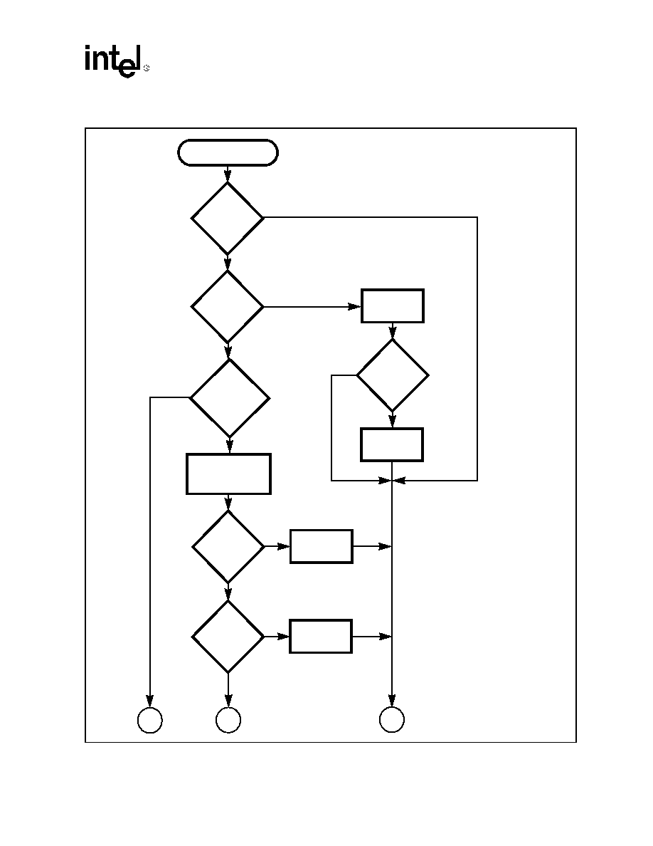
UXART Serial/Parallel Controller -- CD1400
Datasheet
59
Figure 13. CD1400 Transmit Character Processing
Ready for Next
Character
Delay
Time
= `0'
?
Repeat
Char Mode
Active
?
Decrement
count, send
`space'
Count
= 0
?
Clear repeat
Char Mode
Embedded
Command in
Progress
?
Reset Embedded
Command in
Progress
Char
= x'81
?
Char
= x'82
?
Y
Y
Y
Y
Y
Y
N
N
N
N
N
Send
Break
Set Delay
Time
N
A
B
C
(Continued on next page)
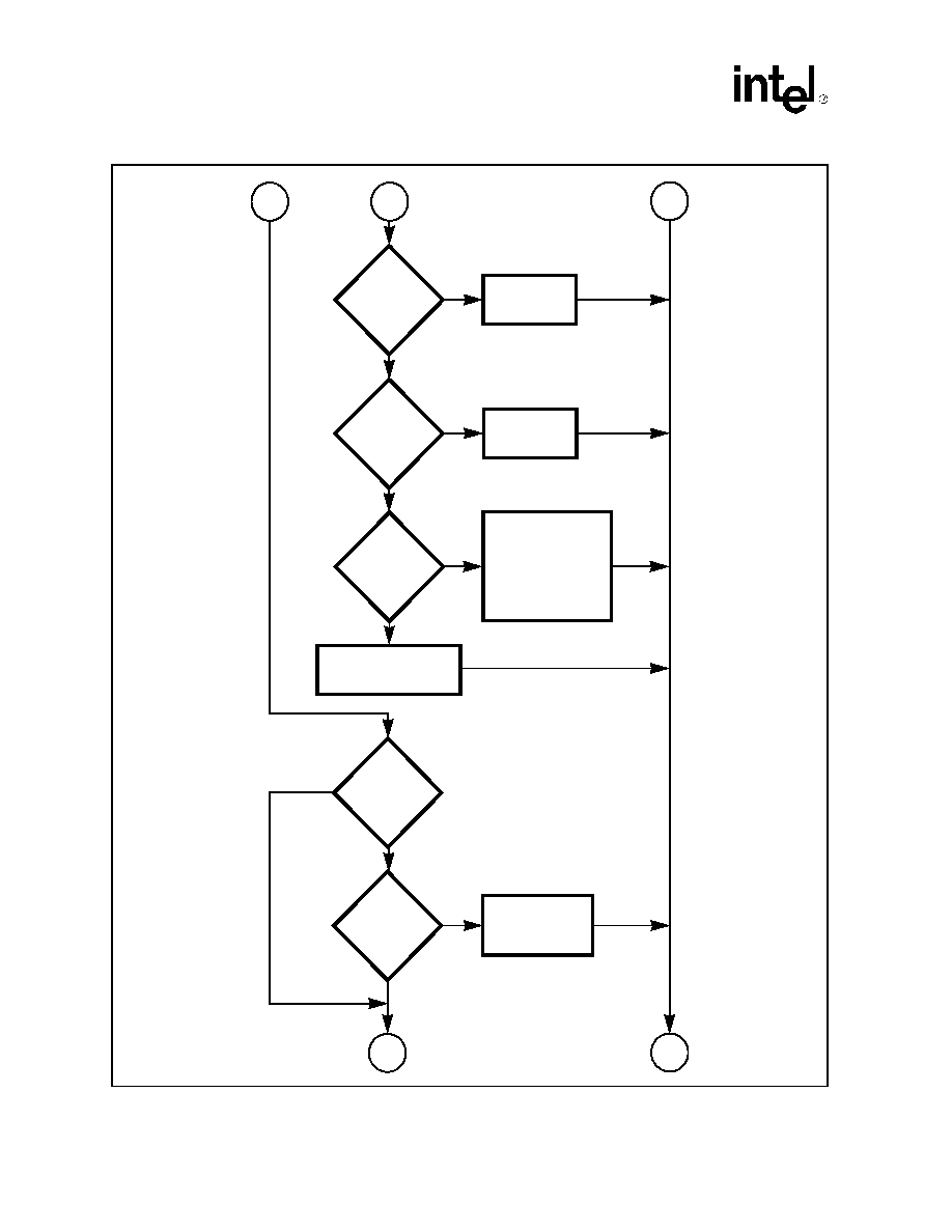
CD1400 -- UXART Serial/Parallel Controller
60
Datasheet
A
B
C
Char
= x'83
?
Char
= x'00
?
Char
= x'01 to x'3F
?
Stop Break
Send `00'
as char
1. Initialize repeat
char count
2. Set repeat
char = `space'
3. Set repeat
Char Mode
Illegal Condition:
Send this as a char
Y
Y
N
N
Y
N
Char
= 00
?
N
Y
ETC
Enabled
?
Y
N
Set Embedded
Command in
progress flag
D
E
(Continued on next page)
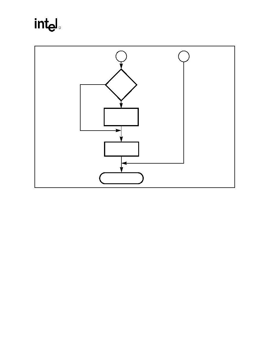
UXART Serial/Parallel Controller -- CD1400
Datasheet
61
7.8
Baud Rate Generation
The CD1400 provides a separate baud rate generator for each direction of each channel. Each
receive and transmit baud rate generator can be driven from one of five available clock sources.
The source being used is selected by the value in the Receive Clock Option Register (RCOR) and
Transmit Clock Option Register (TCOR). The selected clock is divided by the value in the Receive
Baud Rate Period Register (RBPR) or Transmit Baud Rate Period Register (TBPR) to yield the
desired bit rate.
The five clock sources are:
Clk0
System clock divided by 8, RCOR/TCOR = 0
Clk1
System clock divided by 32, RCOR/TCOR = 1
Clk2
System clock divided by 128, RCOR/TCOR = 2
Clk3
System clock divided by 512, RCOR/TCOR = 3
Clk4
System clock divided by 2048, RCOR/TCOR = 4
D
E
Char
Translation
Enabled
?
Perform CR, NL
processing as
specified
Y
N
Send Char
Exit

CD1400 -- UXART Serial/Parallel Controller
62
Datasheet
The system clock is the external clock driving the CLK Input of the CD1400. Four example baud
rate tables are provided at the end of
"Programming" on page 71
.
7.9
Diagnostic Facilities -- Loopback
The CD1400 provides the capability to perform loopback testing internally for both local and
remote loopback modes. Loopback Mode is enabled through the Local Loopback Mode (LLM) and
Remote Loopback Mode (RLM) Bits of COR2.
In local loopback, the output of the transmitter bit engine is connected directly to the input of the
receiver bit engine and the input and output pins (TxD and RxD) are disconnected. The TxD
Output is left in the mark condition so that remote equipment does not sense any line activity. Input
conditions on the RxD are ignored. All channel parameters and service request functions are in
effect and operate normally. If enabled, special characters are detected and acted upon and UNIX
translations occur.
Remote Loopback Mode causes the CD1400 to echo any received data immediately back to the
Transmit Output. This is done character-by-character rather than bit-by-bit; in other words,
characters are echoed once they have been completely received and assembled. Received data will
not be placed in the FIFO, thus no data is given to the host. The received character will be re-
transmitted with parity and Stop Bit options as defined by COR1. It is important to note that, if
transmit baud rate is lower than receive baud rate, overrun errors and loss of data are likely to
occur.
7.10
Parallel Channel Operations
Channel 0 is user-configurable as either a serial or a parallel port. The selection of operating modes
is made by the value of the P/S* Bit (Bit 7) in the Global Configuration Register (GCR). After
reset,
Channel 0 is configured as a serial port by default. Host software reconfigures the port to
the parallel mode by setting this bit to a `1'. The port is capable of bi-directional operation, the
direction being set by the enabled mode: transmit or receive. In the receive mode, the CD1400
drives PBUSY as well as PSTROBE* automatically. PBUSY, however, is not a bi-directional
handshake control: in Transmit Mode, it is not monitored by the CD1400. PACK* is used as the
acknowledge that the transfer has been completed.
It is important to note that when Channel 0 is configured for parallel operation, several of the
modem input signals of the other three channels are taken over for use by the parallel channel to
provide the necessary data and control/status signals required to support the parallel interface
definition of the Centronics parallel specifications. These are the RI and CD Inputs (since they are
used for bidirectional data transfer, they are actually Input/Output Signals). These six signals
(RI[3:1]* and CD[3:1]*) and the two separate Parallel Data Input/Output Signals (PD[0] and
PD[1]) form the bi-directional parallel data port. Other modem input/output signals on Channel 0
provide the control and status signals. The data transfer handshake is provided by the PSTROBE*
Output and the PACK* Input. Note also that these two signals never change direction; PSTROBE*
is always an output and PACK* is always an input. This is the normal signal name convention for
parallel data transmit. For receive, the PSTROBE* Output effectively becomes the Transfer
Acknowledge (ACK) Output function and the PACK* becomes the Data Strobe (STROBE) Input
function.

UXART Serial/Parallel Controller -- CD1400
Datasheet
63
Unlike some parallel interface devices which require the host to control and generate the timing for
the handshake signals directly, the CD1400 automatically generates the PSTROBE* and PBUSY
Outputs and monitors the PACK* Input. This removes nearly all host overhead in data
transmission or reception other than putting data in, or taking data out of, the FIFO. Since parallel
data movement is inherently half-duplex, the CD1400 combines the serial receive and transmit
FIFOs, plus some other registers not needed in Parallel Mode, into one large, 30-byte FIFO. This
further reduces host overhead by providing larger buffering and thus reduced service request
activity.
The width of the PSTROBE* pulse is set by the value programmed in the least-significant five bits
of the TBPR (the TCOR is not used in Parallel Mode) multiplied by the system clock divided by
two. Thus, the width can be any duration in the range of 33.3 ns to 1.03 µs (based on a 60-MHz
system clock, hex values of 1 to 1F in the TBPR). For best overall performance, the RCOR/RBPR
pair should be set to generate a bit-time slightly more than twice the width of the expected pulse on
the PACK* Input. The PBUSY pulse width is dependent on the duration between the Strobe Input
to the CD1400 and the Acknowledge Output (PACK* to PSTROBE* delay; see
"Electrical
Specifications" on page 126
).
General operation of the parallel port is the same as the serial port. When the channel is in the
Transmit Mode and the transmitter and transmit service requests are enabled, the CD1400 will
request service whenever the FIFO is empty. The host responds by writing up to 30 bytes into the
FIFO. Carriage return and new line mapping occur on transmit data in the same manner as in Serial
Mode, if so enabled. Only the send repeated space command of the embedded transmit command
set is operative. The receiver also works the same way in Parallel Mode as it does in serial. The
FIFO threshold can be set to trigger on any level between 1 and 30 inclusive. However, in the
interest of highest possible performance, no receive special character processing occurs.
7.10.1
Transmit Operation
When the channel is enabled for transmit operation and service requests are enabled, the CD1400
will transmit data whenever characters are in the FIFO. Service requests can be programmed to
occur when the FIFO becomes empty. There is no equivalent to the Serial Transmitter Empty
Interrupt in Parallel Mode, thus only the TxRDY Interrupt Bit in the SRER is operational.
Characters are taken directly from the FIFO and placed on the parallel data pins for transmission.
Therefore, when the FIFO is empty (as indicated by the TxRDY Bit in the SRER), there is no more
data to send and the `transmitter' is empty.
Data transmission is controlled by the CD1400 through the handshake signals PSTROBE* and
PACK*. When the FIFO has a byte to send, the CD1400 puts the eight bits of data on the parallel
port. After a 200 ns setup time, the PSTROBE* Signal is driven active (low) and remains active for
the time specified by the value programmed in the TBPR. PSTROBE* is then deactivated and the
data is held until the PACK* Input is driven active (low) by the receiving device. PACK* is the
only signal monitored automatically by the CD1400 for flow-control purposes. The state of
PBUSY, however, is made available to the host through the PSVR. Host software can detect the
busy condition and disable the transmitter, if necessary. Once PACK* becomes inactive, the
CD1400 will place the next data byte on the port (if the FIFO is not empty), and the cycle repeats.
If the receiving device is not able to accept the data, it may hold off the cycle indefinitely by not
activating PACK*. This provides the parallel version of flow control.
Figure 14
shows a typical connection for a CD1400 parallel transmit interface, which is a printer in
this example.
CD1400 -- UXART Serial/Parallel Controller
64
Datasheet
7.10.2
Receive Operation
The receive operation in Parallel Mode is also very much like the Serial Mode. The receive FIFO
has a threshold setting that determines the level of data required to cause a receive service request.
The threshold can be set anywhere from 1 to 30 characters. When the number of characters in the
FIFO equals the set value of the threshold, the CD1400 will post a receive service request.
The sequence of events in receiving a byte is the reverse of sending, the sending device places the
data on the parallel data port; after an appropriate setup time, it activates its strobe out. The strobe
is connected to the PACK* Input of the CD1400. When the CD1400 senses the active level on the
PACK* Input, it activates PBUSY to indicate that it is taking the data but is not yet done. Once it
has taken the data, it will activate its PSTROBE* Output, which should be connected to the sender
acknowledge input. At the end of the programmed pulse width duration (set by TBPR),
PSTROBE* and PBUSY are deactivated.
Flow control happens automatically in the receive direction. If the FIFO is full when the next data
byte is being received, the CD1400 will maintain PBUSY in the active (high) state and will not
activate PACK*. Once the host has serviced the receive FIFO and has removed at least one byte,
thus providing space for the current byte, the CD1400 will complete the receive cycle by
acknowledging the byte (activate PSTROBE*) and deactivating PBUSY.
Figure 15
shows the connections between the CD1400 and a sending device such as a scanner. This
connection might also be seen in an application where the CD1400 is the receiving device in a
printer application.
Figure 14. CD1400 Parallel Data Transmit Connections
DATA
PD[7:0]
PSTROBE*
PACK*
STROBE
ACK
CD1400 PRINTER
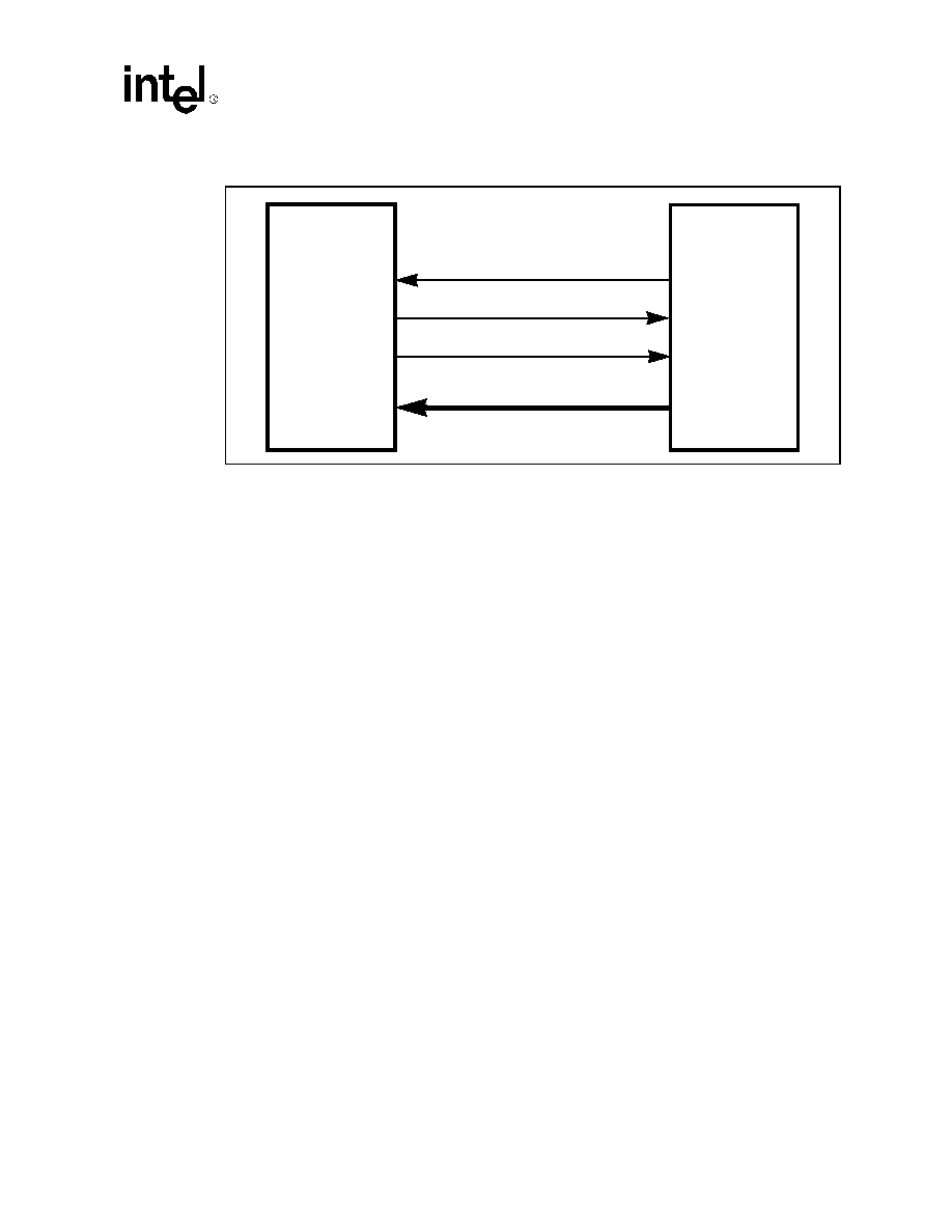
UXART Serial/Parallel Controller -- CD1400
Datasheet
65
7.10.3
Programming Considerations
There are a few guidelines that should be followed for optimum parallel port data transfer
performance. These are primarily related to the programming of the RCOR/RBPR pair, although
programming the TBPR properly also has affects performance.
Only the TBPR is used in determining the pulse width of the PSTROBE* Output when Channel 0
is programmed to be a parallel port; the TCOR is not used and its value is `don't care'. In the
Parallel Mode, the transmit bit engine is not used for PSTROBE* generation. Instead, the
PSTROBE* Output is produced by a five-bit hardware counter that is loaded with the value
contained in the least significant five bits of a register that is itself loaded from the TBPR each time
the channel is enabled (or re-enabled). This five-bit counter is loaded each time a strobe generation
cycle is started. This happens simultaneously with the activation of the PSTROBE* Output. The
counter is decremented once for each cycle of the internal clock (CLK divided by 2); when the
count reaches zero, PSTROBE* is deactivated. In general, the TBPR should be programmed to
produce the shortest pulse width to which the receiving device can reliably respond. Depending
upon the operating frequency of the clock (CLK), the pulse width may be as short as 80 ns (TBPR
= 1, CLK = 60 MHz) to as long as 16 µs (TBPR = 32, CLK = 1 MHz). It is important to note that
any time the strobe width of PSTROBE* is to be changed (that is, a new value is loaded into
TBPR), the change will not be reflected until a channel re-enable, either receive or transmit, is
performed through the CCR.
By far, the programming of the RCOR/RBPR pair will have the most significant impact on parallel
port performance. An explanation of how the device works internally in Parallel Mode will help
make this apparent.
The same bit engine that is used to receive serial data is used to detect the PACK* Signal. When
the CD1400 is waiting for an active PACK* Signal, the bit engine is running in its `Start-Bit
Detect' Mode. In this mode, once it has detected the leading edge of the PACK* Signal, it times to
the middle of the `bit' (one-half bit time, based on the programmed baud rate as determined by the
RCOR/RBPR pair) and then generates an interrupt to the MPU. This would normally be the time
that start-bit validation would take place for serial data. In Parallel Mode, when the MPU executes
the `foreground' routine to service this interrupt, it checks to see if the PACK* Signal is still
present or if it has returned to the inactive state. If it is still active, the foreground process hands the
Figure 15. CD1400 Parallel Data Receive Connections
DATA
PD[7:0]
PSTROBE*
PACK*
ACK
STROBE
CD1400 SCANNER
PBUSY
BUSY
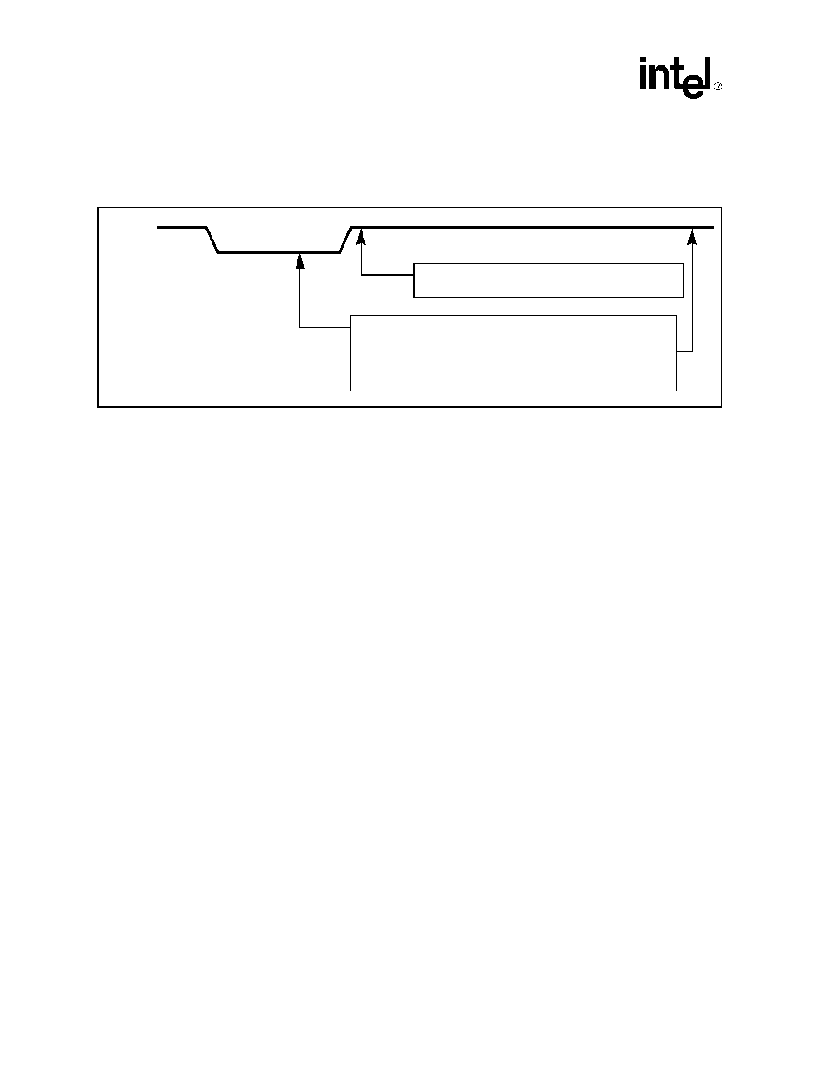
CD1400 -- UXART Serial/Parallel Controller
66
Datasheet
duty of searching for the end of the PACK* to the background task and terminates the interrupt,
since waiting for PACK* to become inactive during foreground processing would seriously
degrade device performance.
If, on the other hand, PACK* has already returned to the inactive state, the MPU can take the
appropriate action immediately, during the foreground loop. In the case of Receive Mode (when
PACK* is actually performing as the strobe input), the MPU retrieves the data from the parallel
port and inserts it directly in the FIFO. If in Transmit Mode, it can allow the background code to
schedule the next character immediately. The ability of the foreground code to handle the
transaction greatly decreases the response time since the background code cycles through all
channels in round-robin fashion. Thus there is a variable delay between each channel's MPU
processing time.
The highest performance will be obtained when the RCOR/RBPR pair are programmed to produce
a bit-time whose half bit-time is just slightly longer than the expected strobe width on the PACK*
Input. In this way, when the foreground process begins execution, the PACK* Input will have
returned to the inactive state and the MPU can handle the data transaction immediately. For
example, if the expected strobe width is 10 µs (100 kbaud), the RCOR/RBPR pair should be
programmed to produce an effective baud rate of a little less than 50K, say 49K to allow for a small
margin of error. To produce this baud rate, the RCOR would be loaded with zero, which selects
clk0 (CLK divided by 8) as the clock source and the RBPR would be loaded with 51 (hex 33).
These numbers assume a 20-MHz system clock (CLK).
The timing diagram in
Figure 16 on page 66
shows the sample point that yields the highest
performance, as explained above.
7.11
Hardware Configurations
The simplicity of the host interface to the CD1400 allows it to be built into systems that use
popular microprocessors, such as the Intel 80x86 family (8086, 80286, 80386, and so on), the
Motorola family (68000, 68010, 68020, and so on), the National 32x32 family (32CG16, 32332,
32532, 32GX32, and so on), and the AMD29000.
Figure 16. Relationship between RCOR/RBPR and PACK* Pulse
PACK*
Sample point for highest performance. Data is
Sampled too early; foreground cannot take the data. Task
given to background code, which will take the data later, at a
time dependent on device activity. Data cannot be acknowl-
edged until data is taken so the cycle extends and no ACK
is generated until the background completes the task.
taken immediately and the ACK can be scheduled.

UXART Serial/Parallel Controller -- CD1400
Datasheet
67
7.11.1
Interfacing to an Intel
Microprocessor-Based System
With little extra logic, the CD1400 can be interfaced to any system based on a processor in the Intel
80x86 family.
Figure 17 on page 68
shows a generalized view of an I/O-mapped interface with an
80286-based system. To provide the proper strobes and controls, the IOR* and IOW* control
strobes are used to synthesize the DS* and R/W* Signals. DTACK* is used as an input to wait-
state generation logic that will hold the processor (if necessary) until the CD1400 has completed
the I/O request.
7.11.2
Interfacing to a Motorola
Microprocessor-Based System
Interfacing to a 68000 family device is straightforward. The bus timing and the interface signal
definitions very closely match those of the 68000 microprocessor, thus allowing direct connection
in most cases. With later versions (68020, 68030), some additional logic is required to generate the
DSACK0* and DSACK1* functions that replace the DTACK* on the earlier devices. The example
in
Figure 18 on page 69
shows a generalized interface to a 68020 device.
7.11.3
Interfacing to a National Semiconductor
Microprocessor-Based
System
The connections between the CD1400 and a NS32000 (32GX320, 32CG16, and so on) embedded
controller are also relatively simple. As with the Intel devices, cycles are controlled by the DS, CS
and R/W Signals that have been synthesized from the available I/O Control Signals and I/O cycle
extensions (wait states) are generated by logic connected to the DTACK Signal. Some additional
consideration is required when implementing memory-mapped I/O to prevent multiple read and
write cycles with the CD1400 FIFOs due to the pipelined architecture of the 32000 device but all of
the necessary controls are available.
Figure 19 on page 70
depicts a simplified interface example.
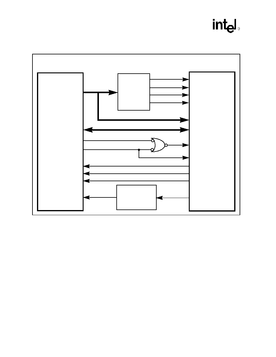
CD1400 -- UXART Serial/Parallel Controller
68
Datasheet
Figure 17.
Intel
80x86 Family Interface
X86
CD1400
SYSTEM
ADDRESS
DECODE
CS*
SVCACKR*
SVCACKT*
SVCACKM*
A[6:0]
DB[7:0]
ADDRESS
DATA
IOR*
IOW*
DS*
R/W*
SVCREQR*
SVCREQT*
SVCREQM*
IRQ
INPUTS
A[23:7]
A[6:0]
WAIT-STATE
GENERATION
LOGIC
READY
DTACK*
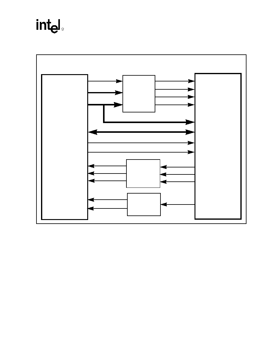
UXART Serial/Parallel Controller -- CD1400
Datasheet
69
Figure 18.
Motorola
68020 Interface
68020
CD1400
SYSTEM
ADDRESS
DECODE
CS*
SVCACKR*
SVCACKT*
SVCACKM*
A[6:0]
DB[7:0]
ADDRESS
DATA
DS*
R/W*
DS*
R/W*
SVCREQR*
SVCREQT*
SVCREQM*
IPL[2:0]
A[31:9]
A[8:2]
DSACK1*
DTACK*
FC[2:0]
PRIORITY
ENCODING
AS*
DSACK0*
TRANSFER
CONTROL
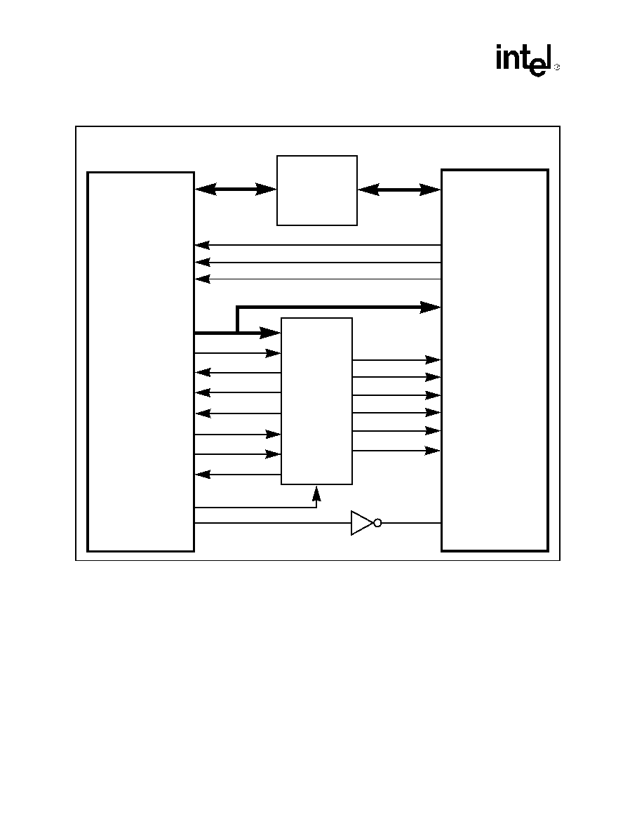
CD1400 -- UXART Serial/Parallel Controller
70
Datasheet
Figure 19.
National
32000 Interface
32000
CD1400
SYSTEM
CS*
SVCACKR*
SVCACKT*
SVCACKM*
A[6:0]
DB[7:0]
DS*
R/W*
SVCREQR*
SVCREQT*
SVCREQM*
DTACK*
DATA
TRANSCEIVER
AND INPUT
LATCH
D[7:0]
ADDRESS
DECODE
IOINH*
IODEC*
BW0
BW1
A[31:0]
DDIN*
CONF*
BMT*
BCLK
AND
CYCLE
CONTROL
BUS
RDY*
INTERRUPT
INPUTS

UXART Serial/Parallel Controller -- CD1400
Datasheet
71
8.0
Programming
8.1
Overview
The CD1400 host interface is made up of a large array of registers that control aspects of chip
behavior; some affect overall chip operations, and some affect only one channel. At first glance,
this can appear to be a bewildering number of registers that need to be manipulated. However, most
of the registers will only be set up once, during initialization, and only rarely modified during
normal operation. The purpose of this section is to discuss these aspects, as well as the methods of
interacting with the CD1400 for channel service needs.
8.2
Initialization
In order to properly bring up a CD1400, several procedures must be completed. These include chip
initialization, programming global functions and setting channel-specific parameters. In most
cases, initialization routines will only be executed once, during overall system boot-up. The
following sections discuss these steps in detail. The flow chart on the next page presents this
information in a visual format.
8.2.1
Chip Initialization
The procedures that perform chip reset will normally be executed after a power-up, system-wide
reset and, therefore, the CD1400 will have performed its own internal initialization, caused by the
Hardware Reset Control Signal, RESET*. If desired, the host may issue a software chip reset to
make sure it has been completed before chip initialization begins. The following steps can be
followed to accomplish this (following the text description, there is a flow chart depicting the same
steps):
1. Wait for CCR to contain 0x00
The contents of the Channel Command Register (CCR) must be zero before a command is
issued. This is required so that any currently executing command has completed before the
new one is started. Since this is probably the first command being written to the CD1400 after
power-on initialization, the CCR is likely to be zero, but it is recommended to always check
the CCR before writing a new command into it.
2. Write hexadecimal 81 (x'81) to the Channel Command Register (CCR).
This command causes the CD1400 to perform an all-channel and global reset. Its effect is to
cause the internal RISC processor to begin execution from its power-up reset location. All
internal host interface registers are cleared, the FIFOs are flushed, and all channels are
disabled.
The all-channel reset command is a special-case CCR operation. Normally, commands issued
to the CCR affect only the channel selected by the CAR. In this case, the setting of the CAR is
not significant.
3. Wait for the firmware revision code to be written into the GFRCR.
This operation is used by the internal firmware to flag completion of the reset procedure. After
reset, the GFRCR is one of the first registers to be cleared and is the last register set before
normal run-time code execution begins. The initialization routine must wait for this register to
become non-zero before beginning any other programming of CD1400 Registers. However, if

CD1400 -- UXART Serial/Parallel Controller
72
Datasheet
the host code is sufficiently fast, it may begin testing the GFRCR before the MPU clears it;
thus, the assumption would be made that the CD1400 has completed its internal initialization
when, in fact, it has not. To avoid this error, the host software should clear the GFRCR just
prior to issuing the global reset and then poll for the correct revision code. This is the
recommended procedure to reset the CD1400.
This procedure can also be used as part of a diagnostic test suite. The device will complete internal
initialization within 500
µ
s. Therefore, a timer (software or hardware) can be used to detect if the
operation does not finish within this time, in which case the chip may not be functional.
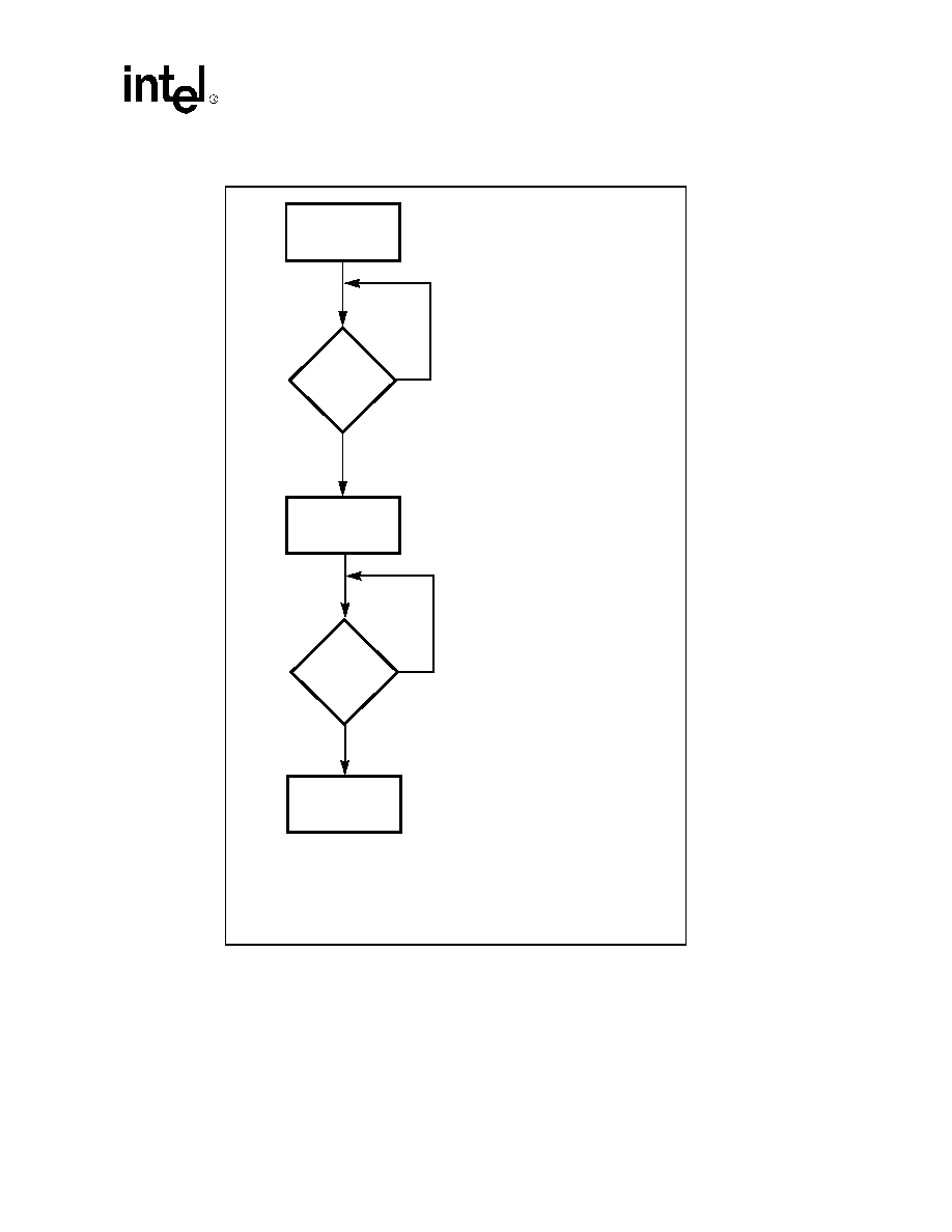
UXART Serial/Parallel Controller -- CD1400
Datasheet
73
8.2.2
Global Function Initialization
Once chip reset has been completed, the next step is to set the Global Operating Mode and timer
pre-scale. All other initialization will take place at the channel level.
1. Set the Global Configuration Register (GCR).
Figure 20. CD1400 Master Initialization Sequence
Issue Reset
Command
GFRCR
= 48*
?
N
Y
Continue
Init Process
* Revision Code for
Revision J device = 48
CCR
= 0
?
N
Y
Clear
GFRCR

CD1400 -- UXART Serial/Parallel Controller
74
Datasheet
The GCR setting determines the mode of operation of Channel 0. After reset, this register is set
to all `0's. This sets Channel 0 to be a serial port. If this is the intended mode for Channel 0,
nothing further needs to be done with this register. If Channel 0 is used as a parallel port, Bit 7
must be set to a `1'.
2. Set the Prescaler Period Register (PPR).
The PPR sets the master time `tick' for the CD1400. It is a binary value that sets the constant
by which the system clock is divided (after a fixed prescale of 512) to produce the internal
clock for the on-chip timers (not the baud rate generators, however). This clock is used for
receiver FIFO time-out generation and delay timing for the insert delay command in the
embedded transmit command set. For example, to generate a timer clock of 1 ms, the value is
computed as:
The value 117 would be loaded into the PPR. This value, in effect, selects an approximate 1-kHz
clock as the source for the Receiver Time-out Period Registers of each channel. Those registers
would, in turn, be loaded with an appropriate value divisor to generate the desired character time-
out periods. This value, 117, is the recommended minimum value that should be placed in the PPR
for a 60-MHz CLK. Values that generate a time period of less than 1 ms adversely affect the
performance of the MPU and, thus, overall serial data performance.
8.2.3
Individual Channel Initialization
At this point, the basic operation of the CD1400 has been set up. The internal register states have
been cleared, the mode for Channel 0 is set, and basic timer operations initialized. The next step is
to program the operating modes of each channel. This includes setting the values for the interrupt
vectors, the receive and transmit baud rates, number of bits per character, number of stop bits,
parity, special characters, if any, and so on. Each channel can have a completely unique set of
operating characteristics. Or, they can all be the same. It is application dependent; the operating
modes of one channel have no effect on the operation of any other (operating Channel 0 as a
parallel port does affect the available input/output signals associated with Channels 1-3 (CD and RI
are borrowed) but not operating characteristics).
The following shows a typical initialization sequence to set up a single serial channel. In this
example, Channel 1 is set up as:
∑
9600 Baud, send and receive
∑
8 bits per character, 1 Stop Bit
∑
No parity
∑
Automatic In-Band (Xon/Xoff) flow control
∑
Transparent flow control
∑
Special character detect enabled
∑
Eight character receive FIFO threshold
∑
Receiver and transmitter enabled for interrupt operation
∑
Enable ISTRIP on incoming characters
60MHz
512
1
ms
◊
117.18
=

UXART Serial/Parallel Controller -- CD1400
Datasheet
75
The clearest way to show this initialization sequence is through a `C' program fragment; the code
shown is compatible with Borland
Turbo C
:
/* Init channel. Channel number is included in call. Register names and addresses
* are defined in the header file (not shown).
*/
init_channel(chan)
char
chan
{
outportb(CAR, chan);
/* set channel number in CAR */
outportb(TCOR, 0x01);
/* constants for 60-MHz clock ≠ clock option*/
outportb(TBPR, 0xc3);
/*
≠ baud rate period */
outportb(RCOR, 0x01);
/* constants for 60-MHz clock ≠ clock option */
outportb(RBPR, 0xc3);
/*
≠ baud rate period */
outportb(COR1, 0x03);
/* no parity, 1 Stop Bit, 8-bit chars */
outportb(COR2, 0x40);
/* auto. in-band flow control */
outportb(COR3, 0x38);
/* transp. flow-control, special char 1 & 2
detect,fifo thresh = 8 */
while (inportb(CCR) != 0)/* make sure that CCR is zero before issuing commands
*/
;
outportb(CCR, 0x4E);
/* issue COR changed command for COR1, 2, 3 */
outportb(COR5, 0x80);
/* enable ISTRIP */
while (inportb(CCR) != 0)
/* make sure that CCR is zero before issuing
commands */
;
outportb(CCR, 0x1A);
/* issue receiver and transmitter enable command to
CCR */
outportb(SRER, 0x14);
/* enable receive and transmit interrupts */
}
8.3
Poll Mode Examples
The CD1400 provides a set of seven registers that are dedicated to Poll Mode operation, as
described in
"Functional Description" on page 29
. This section shows one of many ways in which
these registers can be used to detect and service requests from any of the channel receiver,
transmitter or modem signal change functions.

CD1400 -- UXART Serial/Parallel Controller
76
Datasheet
The primary registers involved in polling are the SVRR, RIR, TIR, MIR and CAR; supplementary
registers are the RIVR, TIVR and MIVR. Of the latter three, only the RIVR is actually used; it
provides the status about whether the service request is for Good Data or exception data. The TIVR
and MIVR provide redundant information and are rarely used. Other registers related to service
requests (TDR, RDSR, MISR, and so on) perform the same functions as they would in a hardware-
acknowledged service request.
Once again, `C' code fragments will be used to describe the functions. As with other coding
examples, it is assumed that register addresses are defined elsewhere, such as in a header file, and
are not shown here. Also, the routines cannot be considered complete. Some pieces will be
dependent on the system software design so liberties are taken in the examples. They do, however,
show methods that can be used to implement the Poll Mode service request/service acknowledge
sequence.
8.3.1
Polling Routine Examples
8.3.1.1
Scanning Loop
/* Poll Mode code fragment. This routine simply checks for any servicing requests
* and branches to the appropriate service routine. The code prioritizes service
* requests as receive, transmit and modem, in that order.
*/
poll( )
{
charstatus;
charrx_stat = tx_stat = md_stat = 0;
if (status = inportb(SVRR)) {
switch (status) {
case 1:
/* all values that include a receive request */
case 3:
case 5:
case 7:
rx_stat = service_rec( );
return(rx_stat);
break;
case 2:
/* all values that include transmit but not receive */
case 6:
tx_stat = service_txm( );

UXART Serial/Parallel Controller -- CD1400
Datasheet
77
return(tx_stat);
break;
case 4:
/* modem service request alone */
md_stat = service_mdm( );
return(md_stat);
break;
default:
/* can't happen :-) */
break;
}
}
}
Once the code above finds an active request posted in the SVRR, it calls the appropriate subroutine
to service the request. The service routines follow.
8.3.1.2
Receive Service
/* The receive service acknowledge cycle begins by reading the RIR. This register
* contains the necessary information to switch the CD1400 into the correct
* service acknowledge context. The RIR is saved for use at the end of the routine
* and then copied into the CAR. The act of copying the RIR into the CAR forces the
* context switch. The channel number requesting service is extracted from the RIR.
* The RIVR Register indicates whether the request is for Good Data or exception
* data and is used to correctly handle the request. At the end of the service, the
* upper two bits in the RIR are cleared causing the switch out of the service
* acknowledge context.
*/
service_rec( )
{
charserv_type, save_rir, save_car, channel, status, char;
int char_count, i;
save_rir = inportb(RIR);
/* retrieve and save receive interrupt value */
channel = save_rir & 0x03;
/* extract channel number from the RIR */
save_car = inportb(CAR);
/* save CAR for restore */
outportb(CAR, save_rir);
/* switch CD1400 to service ack. context */
serv_type = inportb(RIVR) & 0x07;/* read vector register; get type (good/
exception)*/

CD1400 -- UXART Serial/Parallel Controller
78
Datasheet
switch (serv_type) {
case 3:
/* Good Data service */
char_count = inportb(RDCR);
/* get number of characters in FIFO */
for ( i = 1; i <= char_count; i++){
/* - read that number of chars */
char = inportb(RDSR);
/* read char from FIFO */
/* Code here would put the character in a buffer of some sort for each
* channel. That code would be dependent on system software design
* so it won't be shown here. */
}
outportb(RIR, save_rir & 0x3f);/* terminate service ack. sequence */
outportb(CAR, save_car);
/* restore original CAR* /
return(0);
break;
case 7:
/* exception data service request */
status = inportb(RDSR);/* by definition, only one char; get status */
outportb(RIR, save_rir & 0x3f);/* terminate service ack. sequence */
outportb(CAR, save_car);
/* restore original CAR */
return(status);
/* just return the error type */
break;
}
}
8.3.1.3
Transmit Service
/* The transmit service acknowledge routine follows very nearly the same steps that
* the receive service routine follows. This time, the TIR is used to force the
* switch to a transmit service for the requesting channel.
*/
service_txm( )
{
charsave_tir, save_car, channel;
int char_count, i;

UXART Serial/Parallel Controller -- CD1400
Datasheet
79
save_tir = inportb(TIR);
/* retrieve and save transmit interrupt value */
channel = save_tir & 0x03;
/* extract channel number from the TIR */
save_car = inportb(CAR);
/* save CAR for restore */
outportb(CAR, save_tir);
/* switch CD1400 to service ack. context */
/* Buffer management code would set-up pointers to the next 12
* characters (maximum) to be sent on this channel. Again, buffer
* layout is system design dependent and won't be shown here.
*/
for ( i = 0; i < char_count; i++) {/* transmit FIFO can take 12 characters */
outportb(TDR, *next_char++);
/* it is assumed that char_count and next_char is set up by buffer code */
}
outportb(TIR, save_tir & 0x3f);
/* terminate service ack. sequence */
outportb(CAR, save_car);
/* restore original CAR; may not be necessary */
return(0);
}
8.3.1.4
Modem Service
/* Code to handle modem signal change service request can be simple or complex
* depenging on whether port control is handled directly in the service routine or
* simply noted with status returned. The following routine services the request and
* returns the status of which signals changed with the channel number OR'ed into
* the least significant two bits; the main driver software must perform the
* necessary functions. As with the receive and transmit routines,the Interrupt
* Register, this time the MIR, is used to force the CD1400 into the service
* context.
*/
service_mdm( )
{
charsave_mir, channel, save_car, mdm_status;

CD1400 -- UXART Serial/Parallel Controller
80
Datasheet
save_mir = inportb(MIR);
/* retrieve and save modem interrupt value */
channel = save_mir & 0x03;
/* extract channel number from the MIR */
save_car = inportb(CAR);
/* save CAR for restore */
outportb(CAR, save_mir);
/* switch CD1400 to service ack. context */
mdm_status = inportb(MISR);
/* get status of which modem signals changed */
outportb(MIR, save_mir & 0x3f)/* terminate the service ack. sequence */
outportb(CAR, save_car);
/* restore CAR */
return(mdm_status | channel);
}
8.4
Hardware-Activated Service Examples
In nearly all respects, the way in which the host interacts with the CD1400 during hardware
activated service acknowledge is the same as for the software-activated methods. The main
difference is that the SVCACK* Input Signals perform the context switch automatically thus
relieving that duty from the host. The result is the same; the CAR is set to point to the correct
channel and the chip is placed in the proper internal mode to service the request. When the host
activates the SVCACK* Input, a read cycle is performed. The CD1400 places the contents of the
appropriate interrupt vector register (RIVR, TIVR, MIVR) of the channel requesting service on the
data bus. When multiple-CD1400s daisy-chained together, the host uses the information provided
to determine the type of service and the ID number of the device being accessed. At the end of the
service routine, the host writes a dummy value to the EOSRR Register. This causes the switch out
of the service acknowledge context and restores the environment to what it was before the service
began.
The following code fragments show the differences between this type of service acknowledge and
those shown above for the software activated context switch. Only the beginning and ending steps
are shown; the code in between would be very similar to the previous examples. These routines
could be executed as the result of a hardware interrupt or through software polling as in the
previous examples. For purposes of this discussion, the method of arriving at the proper service
routine is not important.
8.4.1
Receive Service
/* The receive service acknowledge cycle begins by executing a service acknowledge
* cycle that activates the SVCACKR* Input. The data obtained as a result of this
* `read' cycle is the contents of the RIVR Register of the channel making the
* service request. The service routine decodes the vector in the least significant
* three bits to determine if the data is `good' or `bad' (exception). The context
* switch was done automatically when the SVCACKR Signal was activated so the CAR
* does not need to be loaded. The routine reads the RICR to determine the
* requesting channel number. If this were a multiple-CD1400 system using daisy-
* chaining, the routine would extract the chip ID from the upper five bits of the
* RIVR.
*/

UXART Serial/Parallel Controller -- CD1400
Datasheet
81
service_rec( )
{
char
serv_type, vector, channel, status, char;
int
char_count, i;
vector = inportb(SVCACKR);
/* gen. ack and get vector (read LIVR) */
channel = inportb(RICR) >> 2;
/* extract channel number from the RICR */
serv_type = vector & 0x07;
/* mask RIVR to get type (good/exception)*/
switch (serv_type) {
case 3:
/* Good Data service */
char_count = inportb(RDCR);
/* get number of characters in FIFO */
for ( i = 1; i <= char_count; i++) {
/* - read that number of chars */
char = inportb(RDSR);
/* read char from FIFO */
/* Code here would put the character in a buffer of some sort for each
* channel. That code would be dependent on system software design
* so it won't be shown here; this code just shows how to manipulate the
* CD1400 registers to implement the poll mode service acknowledge. */
}
break;
case 7:
/* exception data service request */
status = inportb(RDSR);/* by definition, only one char; get status */
break;
}
outportb(EOSRR, 0x00);
/* write dummy value to EOSRR to terminate */
}
8.4.2
Transmit Service
/* The transmit service acknowledge routine closely follows the same steps of the
* receive service routine follows. The SVCACKT* Input is activated to start the
* service cycle, reading the contents of the TIVR, and the TICR is read to get the
* channel number.
*/

CD1400 -- UXART Serial/Parallel Controller
82
Datasheet
service_txm( )
{
charvector, channel;
int char_count, i;
vector = inportb(SVCACKT);/* retrieve and save transmit interrupt value */
channel = inportb(TICR) >> 2;/* extract channel number from the RICR */
/* Buffer management code would setup pointers to the next 12
* characters (maximum) to be sent on this channel. Again, buffer
* layout is system-design-dependent and won't be shown here.
*/
for ( i = 0; i < char_count; i++) {/* transmit FIFO can take 12 characters */
outportb(TDR, *next_char++);
/* it is assumed that char_count and next_char is set up by buffer code */
}
outportb(EOSRR, 0x00); /* write dummy value to EOSRR to terminate */
}
8.4.3
Modem Service
/* The following routine services the modem change service request. Context switch
* is set up by activating the SVCACKM* Input, reading the MIVR. The routine reads
* the MISR Register to determine which modem signal(s) changed. Channel status is
* an externally defined variable that this routine updates.
*/
service_mdm( )
{
charvector, channel;

UXART Serial/Parallel Controller -- CD1400
Datasheet
83
vector = inportb(SVCACKM);/* retrieve and save transmit interrupt value */
channel = inportb(MICR) >> 2;/* extract channel number from the RICR */
mdm_status[channel] = inportb(MISR);/* get status of which modem signals
changed */
outportb(EOSRR, 0x00);/* write dummy value to EOSRR to terminate */
}
8.4.4
Baud Rate Derivation
/* This is a simple code example, which shows a way to derive the proper values for
* the RCOR/TCOR and RBPR/TBPR register pairs for any baud rate. Routine is called
* with the desired baud rate; master clock is fixed; global variables cor and bpr
* are set by the routine.
*/
doublecor_values[ ] = {8.0, 32.0, 128.0, 512.0, 2048.0, -1.0};
compute_baud(baud_rate)
doublebaud_rate;
{
doubleclock = 60000000.0;
int i;
for ( i = 0; cor_values[i] != -1; i++ )
{
brp = (int) ((( clock / baud_rate) / cor_values[i]) + 0.5);
if (brp < 0xFF)
{
cor = i;
bpr = brp;
break;
}
}
return(0);
}
CD1400 -- UXART Serial/Parallel Controller
84
Datasheet
8.5
Baud Rate Tables
The following three tables show the values that need to be loaded into the RCOR/RBPR and
TCOR/TBPR registers to set the designated baud rate when using three standard frequency
crystals. The first one uses a 60-MHz frequency; the second table uses a 25-MHz frequency and
shows error rates that are larger, though still well within the limits set by the various standards of
asynchronous communications. The third uses a 20.2752-MHz frequency, which yields near-
perfect bit rates. It is, of course, not necessary that both the receiver and transmitter of a channel be
programmed to the same baud rate; the CD1400 can send and receive at different rates on the same
channel.
Table 14. Baud Rate Constants, CLK = 60 MHz
Baud Rate
RCOR/TCOR
RBPR/TBPR
(Hex)
Error
134
4
db
0.17%
150
4
C3
0.16%
200
4
92
0.33%
300
4 62
0.35%
600
3
C3
0.16%
1200
3
62
0.35%
1800
3
41
0.16%
2400
2
C3
0.16%
4800
2
62
0.35%
6400
2
49
0.33%
9600
1
C3
0.16%
19200
1
62
0.35%
38400
0
C3
0.16%
56000
0
86
0.05%
57600
0
82
0.16%
64000
0
75
0.16%
76800
0
62
0.35%
115200
0
41
0.16%
128000 0
3b 0.69%
150000 0
32 0.00%
230400 0
21 1.38%
Table 15. Baud Rate Constants, CLK = 25 MHz (Sheet 1 of 2)
Baud Rate
RCOR/TCOR
RBPR/TBPR
(Hex)
Error
110
4
6F
0.02%
150
4
51
0.47%
300
3 A3
0.15%
UXART Serial/Parallel Controller -- CD1400
Datasheet
85
600
3
51
0.47%
1200
2
A3
0.15%
2400
2
51
0.47%
4800
1
A3
0.15%
9600
1
51
0.47%
19200
0
A3
0.15%
38400
0
51
0.47%
56000
0
38
0.35%
57600
0
36
0.47%
64000
0
31
0.35%
76800
0
29
0.76%
115200
0
1B
0.47%
Table 16. Baud Rate Constants, CLK = 20.2752 MHz
Baud Rate
RCOR/TCOR
RBPR/TBPR
(Hex)
Error
110
4
5A
0.00%
150
4
42
0.00%
300
3 84
0.00%
600
3
42
0.00%
1200
2
84
0.00%
2400
2
42
0.00%
4800
1
84
0.00%
9600
1
42
0.00%
19200
0
84
0.00%
38400
0
42
0.00%
56000
0
2D
0.57%
57600
0
2C
0.00%
64000
0
28
1.00%
76800
0
21
0.00%
115200
0
16
0.00%
Table 15. Baud Rate Constants, CLK = 25 MHz (Sheet 2 of 2)
Baud Rate
RCOR/TCOR
RBPR/TBPR
(Hex)
Error

CD1400 -- UXART Serial/Parallel Controller
86
Datasheet
8.6
ASCII Code Table
8.6.1
Hexadecimal -- Character
00
NUL 01
SOH 02
STX 03
ETX 04
EOT 05
ENQ 06
ACK 07
BEL
08
BS
09
HT
0A
NL
0B
VT
0C
NP
0D
CR
0E
SO
0F
SI
10
DLE 11
DC1 12
DC2 13
DC3 14
DC4 15
NAK 16
SYN 17
ETB
18
CAN 19
EM
1A
SUB 1B
ESC 1C
FS
1D
GS
1E
RS
1F
US
20
SP
21
!
22
"
23
#
24
$
25
%
26
&
27
`
28
(
29
)
2A
*
2B
+
2C
,
2D
-
2E
.
2F
/
30
0
31
1
32
2
33
3
34
4
35
5
36
6
37
7
38
8
39
9
3A
:
3B
;
3C
<
3D
=
3E
>
3F
?
40
@
41
A
42
B
43
C
44
D
45
E
46
F
47
G
48
H
49
I
4A
J
4B
K
4C
L
4D
M
4E
N
4F
O
50
P
51
Q
52
R
53
S
54
T
55
U
56
V
57
W
58
X
59
Y
5A
Z
5B
[
5C
\
5D
]
5E
^
5F
_
60
~
61
a
62
b
63
c
64
d
65
e
66
f
67
g
68
h
69
i
6A
j
6B
k
6C
l
6D
m
6E
n
6F
o
70
p
71
q
72
r
73
s
74
t
75
u
76
v
77
w
78
x
79
y
7A
z
7B
{
7C
|
7D
}
7E
_
7F
DEL
8.6.2
Decimal -- Character
0
NUL 1
SOH 2
STX 3
ETX 4
EOT 5
ENQ 6
ACK 7
BEL
8
BS
9
HT
10
NL
11
VT
12
13
13
CR
14
SO
15
SI
16
DLE 17
DC1 18
DC2 19
DC3 20
DC4 21
NAK 22
SYN 23
ETB
24
CAN 25
EM
26
SUB 27
ESC 28
FS
29
GS
30
RS
31
US
32
SP
33
!
34
"
35
#
36
$
37
%
38
&
39
`
40
(
41
)
42
*
43
+
44
,
45
-
46
.
47
/
48
0
49
1
50
2
51
3
52
4
53
5
54
6
55
7
56
8
57
9
58
:
59
;
60
<
61
=
62
>
63
?
64
@
65
A
66
B
67
C
68
D
69
E
70
F
71
G
72
H
73
I
74
J
75
K
76
L
77
M
78
N
79
O

UXART Serial/Parallel Controller -- CD1400
Datasheet
87
80
P
81
Q
82
R
83
S
84
T
85
U
86
V
87
W
88
X
89
Y
90
Z
91
[
92
\
93
]
94
^
95
_
96
~
97
a
98
b
99
c
100 d
101 e
102 f
103 g
104 h
105 i
106 j
107 k
108 l
109 m
110 n
111 o
112 p
113 q
114 r
115 s
116 t
117 u
118 v
119 w
120 x
121 y
122 z
123 {
124 |
125 }
126 _
127 DEL
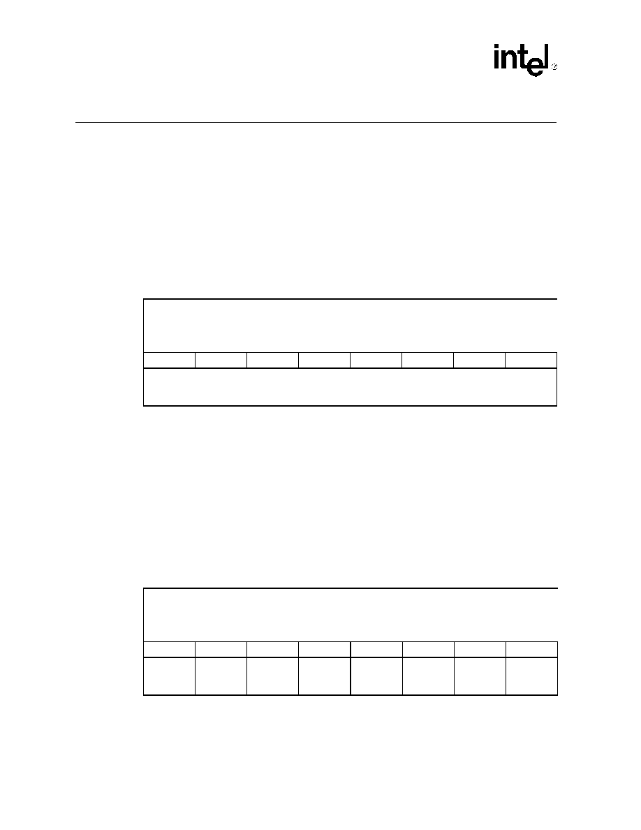
CD1400 -- UXART Serial/Parallel Controller
88
Datasheet
9.0
Detailed Register Descriptions
This section presents a complete, detailed description of each register. Registers have two formats:
full eight bits, where the entire content defines a single function; or, the register is a collection of
bits, grouped singly or in multiples, defining a function. In the second case, the descriptions break
the register down into its component parts and describe the bits individually. The order of register
presentation follows that given in the brief register descriptions in
"Registers" on page 22
.
9.1
Global Registers
9.1.1
Global Firmware Revision Code (GFRCR)
The GFRCR serves two purposes in the CD1400. First, it displays the revision number of the
firmware in the chip. When a revision to the CD1400 is required, the revision number of the
firmware is incremented by one. The code is 48 for the Revision J device. Later revisions, if
necessary, will increment this by one; for example, Revision K will be 49, and so on.
Secondly, this register can be used by the system programmer as an indication of when the internal
processor has completed reset procedures, after either a power-on reset (through the Reset* Input)
or a software global reset (through the reset command in the CCR). Immediately after the reset
operation begins, the internal CPU clears the register. When complete, and the CD1400 is ready to
accept host accesses, the register is loaded with the revision code.
9.1.2
Channel Access Register (CAR)
Register Name: GFRCR
Hex Address: 40
Register Description: Global Firmware Revision Code
Default Value: x'48
Access: Read/Write
Bit 7
Bit 6
Bit 5
Bit 4
Bit 3
Bit 2
Bit 1
Bit 0
Firmware revision code
Register Name: CAR
Hex Address: 68
Register Description: Channel Access
Default Value: x'C0
Access: Read/Write
Bit 7
Bit 6
Bit 5
Bit 4
Bit 3
Bit 2
Bit 1
Bit 0
poll
poll
poll
poll
poll
0
C1
C0
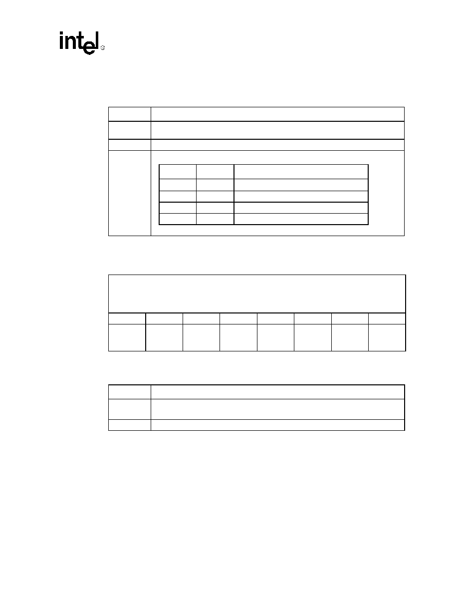
UXART Serial/Parallel Controller -- CD1400
Datasheet
89
The CAR provides access to individual channels within the CD1400. The least significant two bits
of the register selects one of the four channels. Before any operation that affects a channel, this
register must be loaded so that Channel Registers are available to the host.
9.1.3
Global Configuration Register (GCR)
The GCR is used to define the mode of operation for Channel 0. Resetting Bit 7 will select Serial
Mode; setting Bit 7 selects parallel. The default mode selection after reset is serial.
Bit
Description
Bits 7:3
Bits 7:3 are not used except during Poll Mode operation (see
"Functional Description" on
page 29
for details).
Bit 2
Bit 2 must always be `0'.
Bits 1:0
Register Name: GCR
Hex Address: 4B
Register Description: Global Configuration
Default Value: x'00
Access: Read/Write
Bit 7
Bit 6
Bit 5
Bit 4
Bit 3
Bit 2
Bit 1
Bit 0
P/S*
0
0
0
0
0
0
0
C1
C0
Channel number
0
0
Channel 0
0
1
Channel 1
1
0
Channel 2
1
1
Channel 3
Bit
Description
Bit 7
P/S* = 0 Channel 0 Mode is serial
P/S* = 1 Channel 0 Mode is parallel
Bits 6:0
Must be `0'.
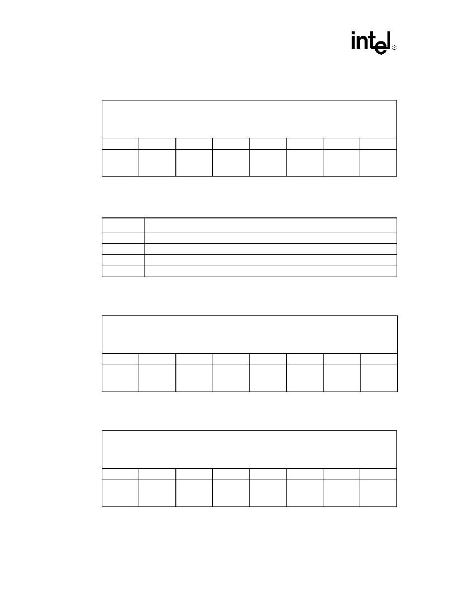
CD1400 -- UXART Serial/Parallel Controller
90
Datasheet
9.1.4
Service Request Register (SVRR)
The SVRR reflects the inverse of the state of the Service Request Pins (SVCREQR*, SVCREQT*
and SVCREQM*). Its primary use is in polled systems, and it allows system software to determine
what, if any, service requests are pending.
9.1.5
Receive Interrupting Channel Register (RICR)
9.1.6
Transmit Interrupting Channel Register (TICR)
Register Name: SVRR
Hex Address: 67
Register Description: Service Request
Default Value: x'00
Access: Read only
Bit 7
Bit 6
Bit 5
Bit 4
Bit 3
Bit 2
Bit 1
Bit 0
0
0
0
0
0
SRM
SRT
SRR
Bit
Description
Bits 7:3
Always `0'
Bit 2
Service Request Modem; `1' indicates request pending.
Bit 1
Service Request Transmit; `1' indicates request pending.
Bit 0
Service Request Receive; `1' indicates request pending.
Register Name: RICR
Hex Address: 44
Register Description: Receive Interrupting Channel
Default Value: x'00
Access: Read/Write
Bit 7
Bit 6
Bit 5
Bit 4
Bit 3
Bit 2
Bit 1
Bit 0
X
X
X
X
C1
C0
X
X
Register Name: TICR
Hex Address: 45
Register Description: Transmit Interrupting Channel
Default Value: x'00
Access: Read/Write
Bit 7
Bit 6
Bit 5
Bit 4
Bit 3
Bit 2
Bit 1
Bit 0
X
X
X
X
C1
C0
X
X
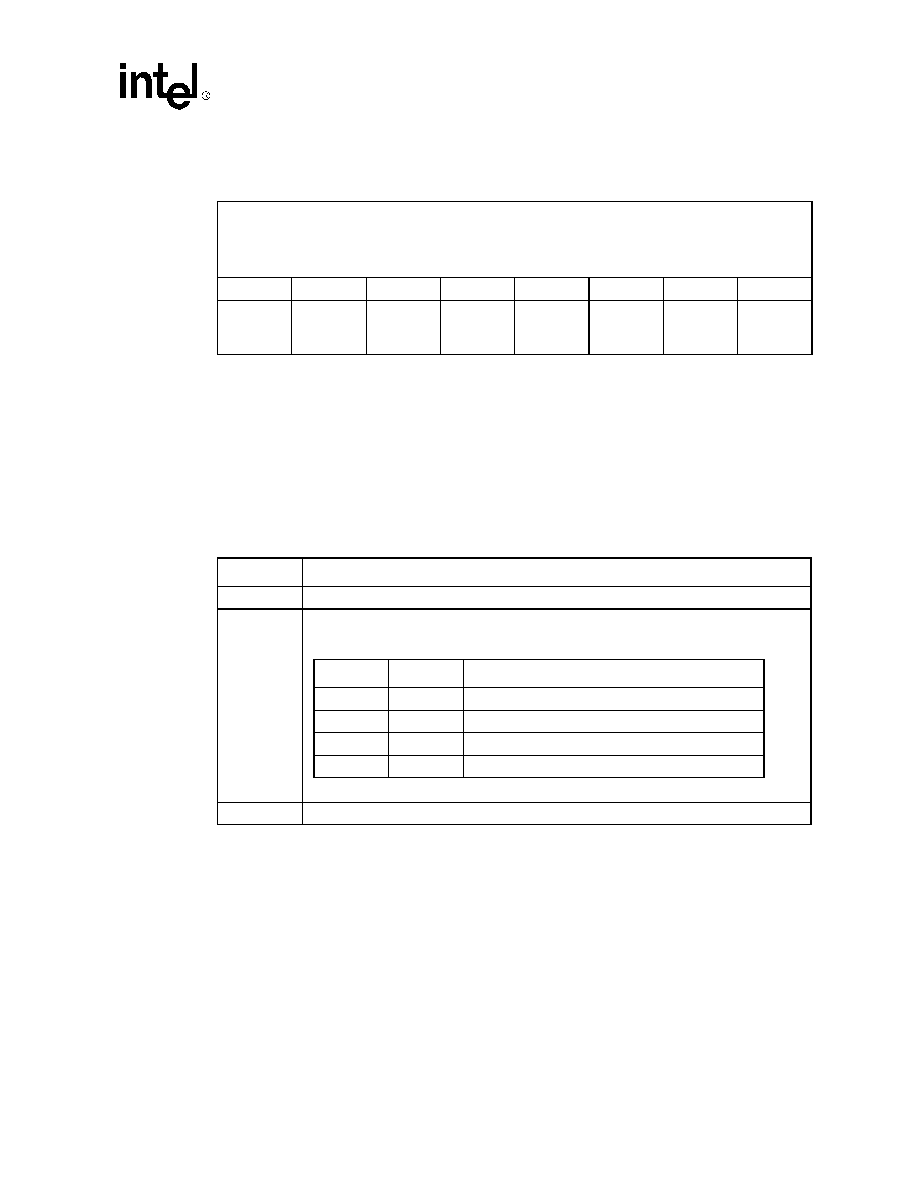
UXART Serial/Parallel Controller -- CD1400
Datasheet
91
9.1.7
Modem Interrupting Channel Register (MICR)
These registers indicate the channel number that is currently being serviced by an active
acknowledge cycle (whether polled or interrupt). Bits 3-2 (C1 and C0) are valid only during the
context of a channel service routine; at any other time, their state is undefined. Host system
software uses these registers to determine the number of the channel that originated the particular
service request (receive, transmit or modem). The format of these registers is the same and the
description is valid for each. The upper four bits and lower two bits are user-defined and may be set
to any value desired. When the register is read, these bits will be presented as defined by the user;
C1 and C0 will be set by the CD1400 to reflect the proper channel number. For further information
refer to
Table 17
.
Register Name: MICR
Hex Address: 46
Register Description: Modem Interrupting Channel
Default Value: x'00
Access: Read/Write
Bit 7
Bit 6
Bit 5
Bit 4
Bit 3
Bit 2
Bit 1
Bit 0
X
X
X
X
C1
C0
X
X
Table 17.
Receive/Transmit/Modem Interrupting Channel Registers
Bit
Description
Bits 7:4
User-defined.
Bits 3:2
Defines Channel Number
.
Bits 1:0
User-defined.
C1
C0
Channel number
0
0
Channel 0
0
1
Channel 1
1
0
Channel 2
1
1
Channel 3
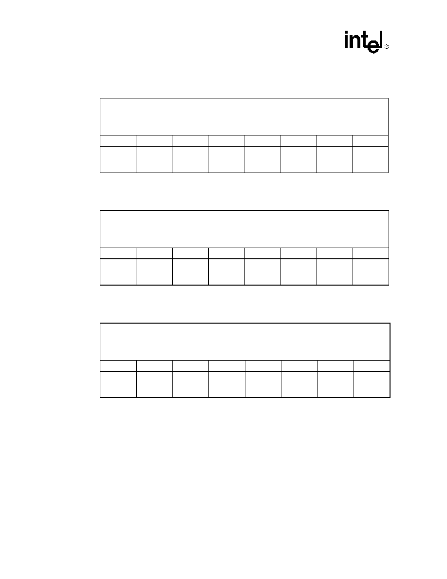
CD1400 -- UXART Serial/Parallel Controller
92
Datasheet
9.1.8
Receive Interrupt Register (RIR)
9.1.9
Transmit Interrupt Register (TIR)
9.1.10
Modem Interrupt Register (MIR)
These registers are used during Poll Mode operation of the CD1400. All three provide the same
type of information for each of the three service requests. The functions of rxireq, txireq and
mdireq have identical meanings, as do the group rbusy, tbusy and mbusy and the group runfair,
tunfair and munfair. The least significant two bits indicate the number of the channel requesting
service. Bits 2 through 4 are used internally by the CD1400 to set the context of the service
acknowledge cycle. See the description of Poll Mode operation in
"Programming" on page 71
for
complete details.
Register Name: RIR
Hex Address: 6B
Register Description: Receive Interrupt
Default Value: x'18
Access: Read/Write
Bit 7
Bit 6
Bit 5
Bit 4
Bit 3
Bit 2
Bit 1
Bit 0
rxireq
rbusy
runfair
1
1
0
ch[1]
ch[0]
Register Name: TIR
Hex Address: 6A
Register Description: Transmit Interrupt
Default Value: x'10
Access: Read/Write
Bit 7
Bit 6
Bit 5
Bit 4
Bit 3
Bit 2
Bit 1
Bit 0
txireq
tbusy
tunfair
1
0
0
ch[1]
ch[0]
Register Name: MIR
Hex Address: 69
Register Description: Modem Interrupt
Default Value: x'08
Access: Read/Write
Bit 7
Bit 6
Bit 5
Bit 4
Bit 3
Bit 2
Bit 1
Bit 0
mdireq
mbusy
munfair
0
1
0
ch[1]
ch[0]
UXART Serial/Parallel Controller -- CD1400
Datasheet
93
9.1.11
Prescaler Period Register (PPR)
The PPR sets the divisor that will be used to generate the time period for CD1400 timer operations.
It can be set to any value between 0 and 255 (x'FF). The PPR is clocked by the system clock
prescaled (divided) by 512. Note that this value does not have any effect on baud rate generation.
The time period generated by this register drives the receive timer and is used to activate the `no
new data' and `receive data time-out' interrupts. See the receiver operation discussion in
"Receiver
Timer Operations" on page 40
for a description of receiver timer functions.
Bit
Description
Bit 7
rxireq, txireq, mdireq: These bits are set by the internal processor when service is required
by a channel. They are a direct reflection of the inverse state of the SVCACK* Pins, and they
are not actually part of the register but are the active-high output of the latch that drives the
SVCACK* Pins. The bits can be scanned by the host to detect an active service request.
These bits are cleared by the internal processor at the beginning of the service acknowledge
cycle (hardware service acknowledge) or by the host software when the Poll Mode cycle is
terminated.
Bit 6
rbusy, tbusy, mbusy: These bits are set by the internal processor and remain set until the
end of the service acknowledge cycle is indicated by either a write to the EOSRR (hardware
service acknowledge), or cleared by the host software when the Poll Mode cycle is terminated.
They signal the current state of the service acknowledge cycle. When cleared, the internal
processor senses that it can assert another service request of this type.
Bit 5
runfair, tunfair, munfair: These bits are used by the internal processor to implement the `Fair
Share' service request function. If this bit is set, the CD1400 will not assert another service
request of this type until the bit is cleared by a pulse on the external SVCACK* Pin. These bits
are not used in Poll Mode.
Bits 4:2
These bits define the context of the current service acknowledge cycle during Poll Mode and
are fixed by hardware within the CD1400. These bits must be replicated exactly when the
register is copied to the CAR when activating a service acknowledge cycle. See the
discussion of Poll Mode operation in
"Registers" on page 22
for a more detailed description.
Bits 1:0
ch[1] - ch[0]: These two bits encode the channel number of the requesting channel. During
Poll Mode operation, when the RIR, TIR and MIR are copied into the CAR to start the service
routine, ch[1:0] set the channel number that will be serviced.
Register Name: PPR
Hex Address: 7E
Register Description: Prescaler Period
Default Value: x'FF
Access: Read/Write
Bit 7
Bit 6
Bit 5
Bit 4
Bit 3
Bit 2
Bit 1
Bit 0
Binary Value
CD1400 -- UXART Serial/Parallel Controller
94
Datasheet
9.2
Virtual Registers
The CD1400 has two operational contexts, a normal context that allows host access to most
registers and any channel, and a service acknowledge context, allowing host access to some
registers specific to the channel requesting service. This special set of registers is called virtual
because they are only available to host access and valid during this service acknowledge context; at
all other times, their contents will be undefined and must not be written to by host software.
The use of virtual registers and context switching allows the CD1400 to maintain all channel-
specific information. The host need not make any changes to chip registers in order to access the
registers pertinent to the channel being serviced.
The service acknowledge context is entered into in one of two ways; either via activation of one of
the SVCACK* Input Pins (hardware-activated), or via host software when the contents of any one
of TIR, RIR or MIR is copied into the CAR by host software during a Poll Mode acknowledge
cycle. See
"Functional Description" on page 29
for a discussion of the differences between these
two modes.
9.2.1
Receive Interrupt Vector Register (RIVR)
9.2.2
Transmit Interrupt Vector Register (TIVR)
Register Name: RIVR
Hex Address: 43
Register Description: Receive Interrupt Vector
Default Value: x'00
Access: Read only
Bit 7
Bit 6
Bit 5
Bit 4
Bit 3
Bit 2
Bit 1
Bit 0
X
X
X
X
X
IT2
IT1
IT0
Register Name: TIVR
Hex Address: 42
Register Description: Transmit Interrupt Vector
Default Value: x'00
Access: Read only
Bit 7
Bit 6
Bit 5
Bit 4
Bit 3
Bit 2
Bit 1
Bit 0
X
X
X
X
X
IT2
IT1
IT0
UXART Serial/Parallel Controller -- CD1400
Datasheet
95
9.2.3
Modem Interrupt Vector Register (MIVR)
These registers serve the same function for each of their respective service types -- receive,
transmit and modem. They provide information about the service request that is being
acknowledged.
The upper five bits are user-defined, as programmed via the LIVR Register of the channel being
serviced; the lower three bits provide the service acknowledge vector and are OR'ed in by the
CD1400 when the register is read. The use of the TIVR and MIVR is optional if the value
contained in the upper five bits is not needed by host software. The vector provided will be as
indicated for the particular interrupt. IT2-IT0 will indicate that the service is for transmit in the case
of the TIVR and modem for the MIVR. The value of these bits will be important when servicing a
receive service request; IT2-IT0 will indicate whether the service request is for Good Data or
`exception' data. The table on the following page shows the encoding of IT2-IT0. For further
information, refer to
Table 18
.
Register Name: MIVR
Hex Address: 41
Register Description: Modem Interrupt Vector
Default Value: x'00
Access: Read only
Bit 7
Bit 6
Bit 5
Bit 4
Bit 3
Bit 2
Bit 1
Bit 0
X
X
X
X
X
IT2
IT1
IT0
Table 18.
Receive/Transmit/Modem Interrupt Vector Registers
Bit
Description
Bits 7:3
User defined.
Bits 2:0
IT2
IT1
IT0 Group/Type
0
0
0 Not
used
0
0
1
Group 1: Modem Signal change service request
0
1
0
Group 2: Transmit data service request
0
1
1
Group 3: Received Good Data service request
1
0
0 Not
used
1
0
1 Not
used
1
1
0 Not
used
1
1
1
Group 3: Received exception data service
request
CD1400 -- UXART Serial/Parallel Controller
96
Datasheet
9.2.4
Transmit Data Register (TDR)
The Transmit Data Register is the host port for writing to the transmit FIFO. When a channel is
being serviced for a transmit service request, the host may write up to twelve characters into this
register. The Transmit Data Register must only be written to during the context of a transmit
service acknowledge. Writing data to this location at any other time will have unpredictable results.
9.2.5
Receive Data/Status Register (RDSR)
9.2.6
Receive Data/Status Register (RDSR)
The Receive Data and Status Register serves two purposes. During a receiver service acknowledge
for good data, the RDSR provides access to the receive FIFO. The number of characters available
in the FIFO is indicated by the Receive Data Count Register (RDCR), which is described in the
following section. Any number of characters, up to the value in the RDCR, may be read from the
FIFO. All internal FIFO pointers are updated by the on-chip processor.
Register Name: TDR
Hex Address: 63
Register Description: Transmit Data
Default Value: x'00
Access: Write only
Bit 7
Bit 6
Bit 5
Bit 4
Bit 3
Bit 2
Bit 1
Bit 0
Transmit Character
Register Name: RDSR
Hex Address: 62
Register Description: Receive Data
Default Value: x'00
Access: Read only
Bit 7
Bit 6
Bit 5
Bit 4
Bit 3
Bit 2
Bit 1
Bit 0
Received Character
Register Name: RDSR
Hex Address: 62
Register Description: Status
Default Value: x'00
Access: Read only
Bit 7
Bit 6
Bit 5
Bit 4
Bit 3
Bit 2
Bit 1
Bit 0
Time-out
SC Det2
SC Det1
SC Det0
Break
PE
FE
OE
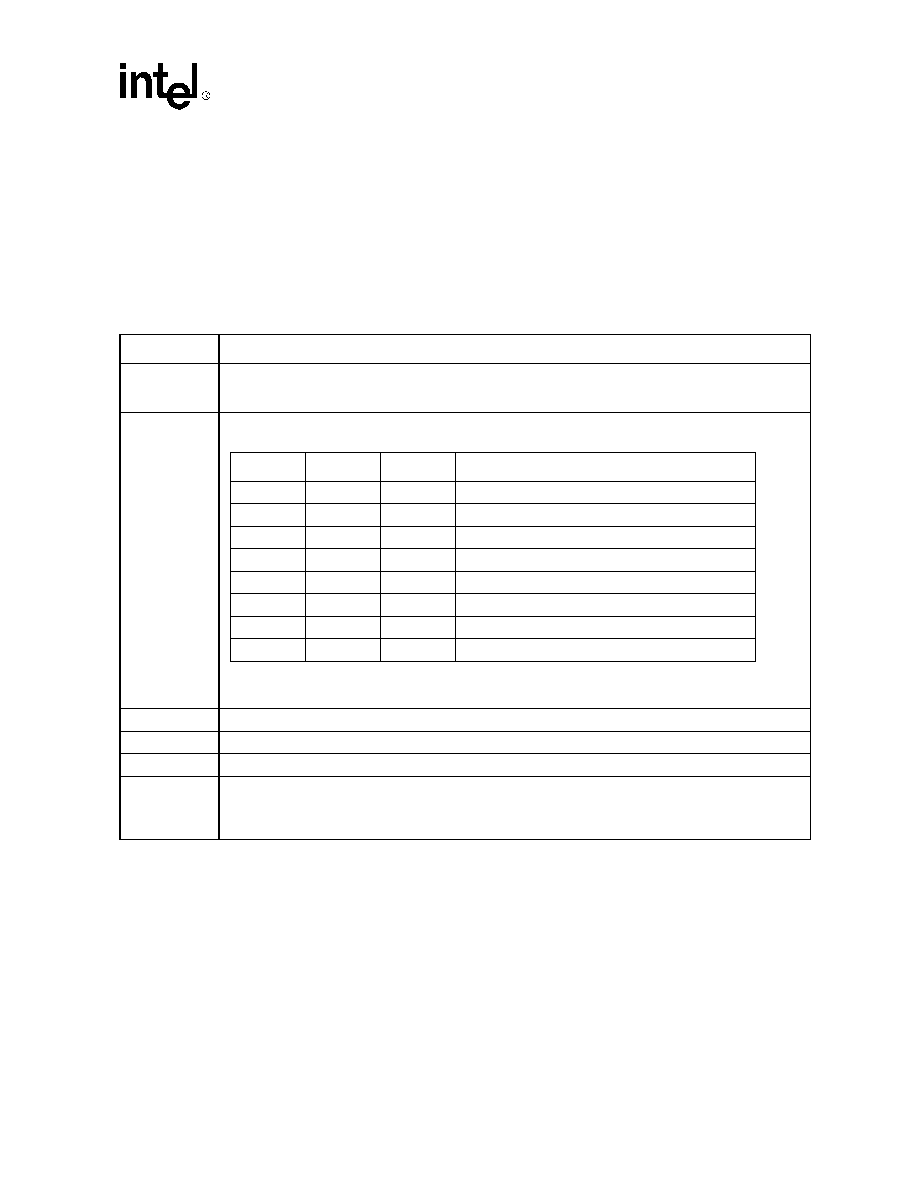
UXART Serial/Parallel Controller -- CD1400
Datasheet
97
During a receive exception service acknowledge, the RDSR provides both the received character
and the status that caused the exception condition. By definition, a receive exception service
request will have only one character available (multiple receive exceptions will produce multiple
service requests). The first read from the RDSR will provide the exception status, and the second
read will provide the character. It is not necessary to read either of these values. If the service
acknowledge is terminated without reading any data from the RDSR, the internal processor will
update the FIFO pointers as if the status/character were read. The same is true if only the status is
read. Overrun errors are an exception to this (see next page). For further information, refer to
Table
19
.
Table 19.
Receive Data/Status Register
Bit
Description
Bit 7
Time-out: If the service request enable for time-out is set, this bit will indicate that no data has been received
within the receive time-out period set by the Receive Time-out Period Register (RTPR) after the last character
was removed.
Bits 6:4
Special Character Detect Encoding
NOTE: No special character matching is performed if either a parity (PE) or framing (FE) error occur unless
CMOE is enabled via COR5 (Bit 5).
Bit 3
Break: Indicates that a break was detected.
Bit 2
Parity Error: Indicates that a character was received with parity other than that programmed in COR 1.
Bit 1
Framing Error: Indicates that the character was received with a bad stop bit.
Bit 0
Overrun Error: This bit will be set if new data is received, but there is no space available in the FIFO and
Holding Register. In this case, the character data is lost, and the overrun flag is applied to the last good data
received before the overrun occurred. Thus, the character read on the subsequent read from the RDSR is
good data and should not be discarded.
SCDet2
SCDet1
SCDet0 Status
0
0
0 None
Detected
0
0
1
Special Character 1 matched
0
1
0
Special Character 2 matched
0
1
1
Special Character 3 matched
1
0
0
Special Character 4matched
1
0
1 Not
used
1
1
0
End of Break Detected
1
1
1 Range
Detect
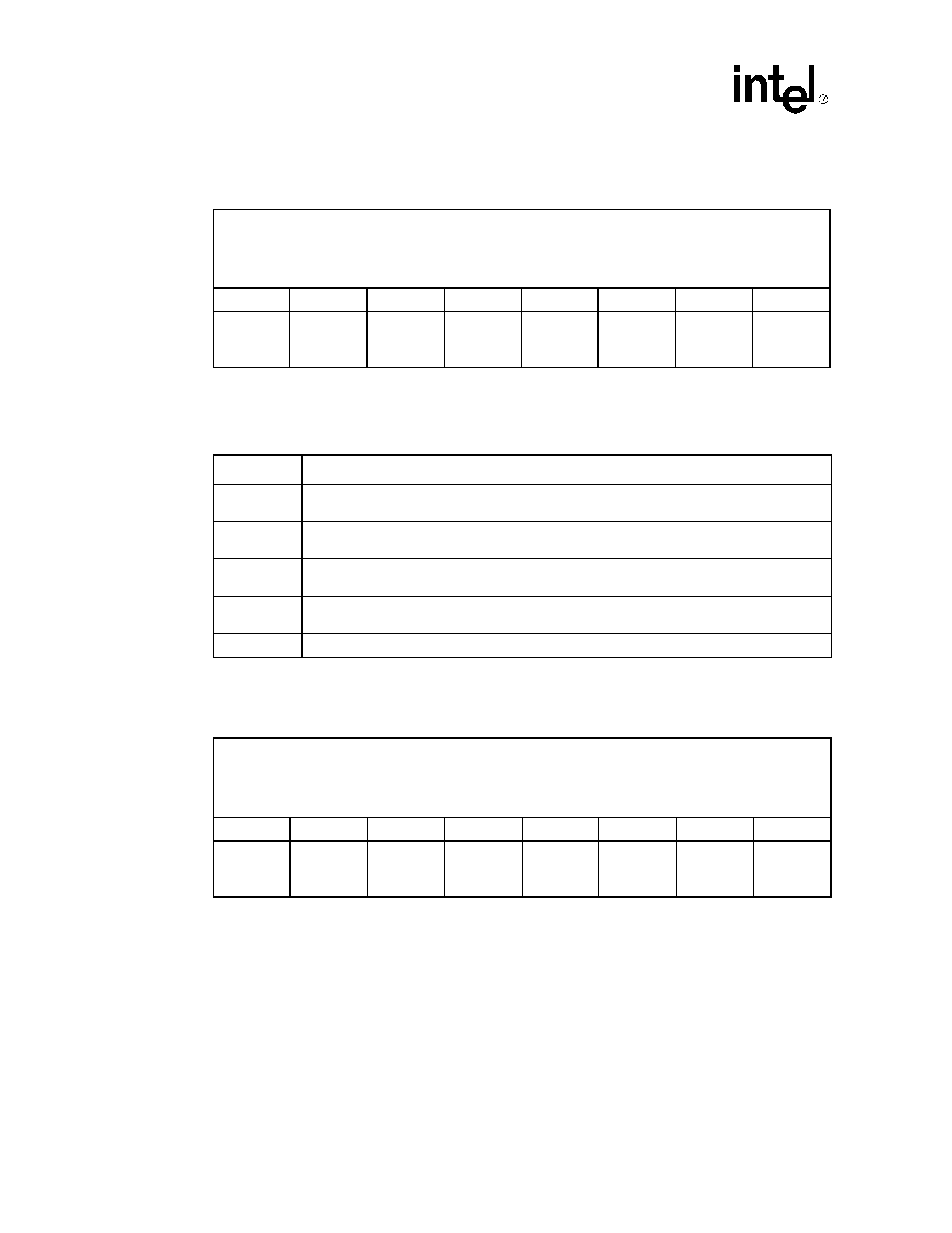
CD1400 -- UXART Serial/Parallel Controller
98
Datasheet
9.2.7
Modem Interrupt Status Register (MISR)
The MISR provides the status indication of the reason for a modem service request. If either or
both of the Modem Change Modes (zero-to-one or one-to-zero transition) are enabled, such a
change will cause a service request, and the signal that changed will be flagged in this register.
9.2.8
End Of Service Request Register (EOSRR)
The EOSRR is a dummy location and is used to signal the end of a hardware service acknowledge
procedure, activated via one of the SVCACK* Pins. The data pattern written is a `don't care' value.
The action of writing this location causes the CD1400 to perform its internal switch out of the
service acknowledge context. This register is only used during a hardware-activated service
acknowledge and must not be written during Poll Mode operation.
Register Name: MISR
Hex Address: 4C
Register Description: Modem Interrupt Status
Default Value: x'00
Access: Read only
Bit 7
Bit 6
Bit 5
Bit 4
Bit 3
Bit 2
Bit 1
Bit 0
DSRch
CTSch
RIch
CDch
0
0
0
0
Bit
Description
Bit 7
DSR change: An enabled transition on the Data Set Ready Signal will cause this bit to be set
and a modem service request posted.
Bit 6
CTS change: An enabled transition on the Clear To Send Signal will cause this bit to be set
and a modem service request posted.
Bit 5
RI change: An enabled transition on the Ring Indicator Signal will cause this bit to be set and
a modem service request posted.
Bit 4
CD change: An enabled transition on the Carrier Detect Signal will cause this bit to be set and
a modem service request posted.
Bits 3:0
These bits will always return zero.
Register Name: ESORR
Hex Address: 60
Register Description: End Of Service Request
Default Value: x'00
Access: Write only
Bit 7
Bit 6
Bit 5
Bit 4
Bit 3
Bit 2
Bit 1
Bit 0
X
X
X
X
X
X
X
X
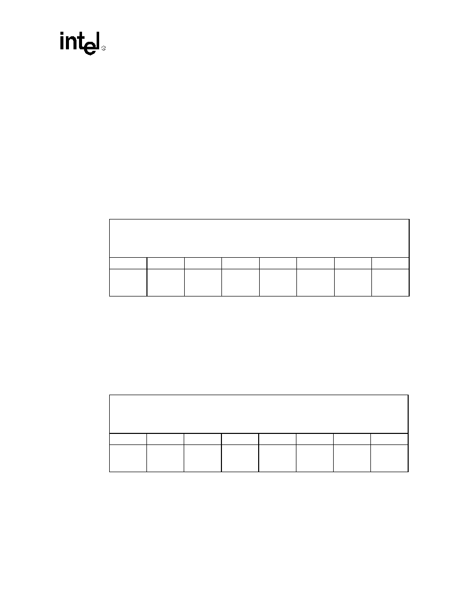
UXART Serial/Parallel Controller -- CD1400
Datasheet
99
9.3
Channel Registers
Each of the four channels has a set of registers that control aspects of its operation. In the
information below, the register contents and offsets apply to any of the channels; the channel being
accessed at any given time is controlled by the CAR. This holds true even during a service
acknowledge context; the CAR points to the channel be serviced, whether it was loaded by the host
(during Poll Mode operations) or by the CD1400 itself (during hardware-activated service
acknowledge cycles).
In a few of the following cases, some of the registers show two formats, one for serial and one for
parallel. In these cases, the parallel register format applies only to Channel 0, and only when the
GCR has been programmed to place Channel 0 in Parallel Mode.
9.3.1
Local Interrupt Vector Register (LIVR)
The LIVR is used only during hardware-activated service acknowledge cycles. Host software loads
any information desired into the most significant five bits; the least significant three bits are not
used. When the CD1400 is setting up a service request, it overlays the five significant bits of the
LIVR into the appropriate Interrupt Vector Register (RIVR, TIVR and MIVR) and sets the least
significant three bits as required for the service request vector type. (See the RIVR, TIVR and
MIVR descriptions earlier in this section).
9.3.2
Channel Command Register (CCR)
The Channel Command Register is used to issue commands directly to the on-chip processor to
control or change some channel and, in one case, global functions of the channel selected by the
CAR. The upper four bits indicate which of four command types is being issued, and the lower four
bits are parameters to those commands. At no time should more than one bit be set in the command
Register Name: LIVR
Hex Address: 18
Register Description: Local Interrupt Vector
Default Value: x'00
Access: Read/Write
Bit 7
Bit 6
Bit 5
Bit 4
Bit 3
Bit 2
Bit 1
Bit 0
X
X
X
X
X
IT2
IT1
IT0
Register Name: CCR
Hex Address: 05
Register Description: Channel Command Register
Default Value: x'00
Access: Read/Write
Bit 7
Bit 6
Bit 5
Bit 4
Bit 3
Bit 2
Bit 1
Bit 0
Res Chan
COR Chg
Send SC
Chan Ctl
D3
D2
D1
D0
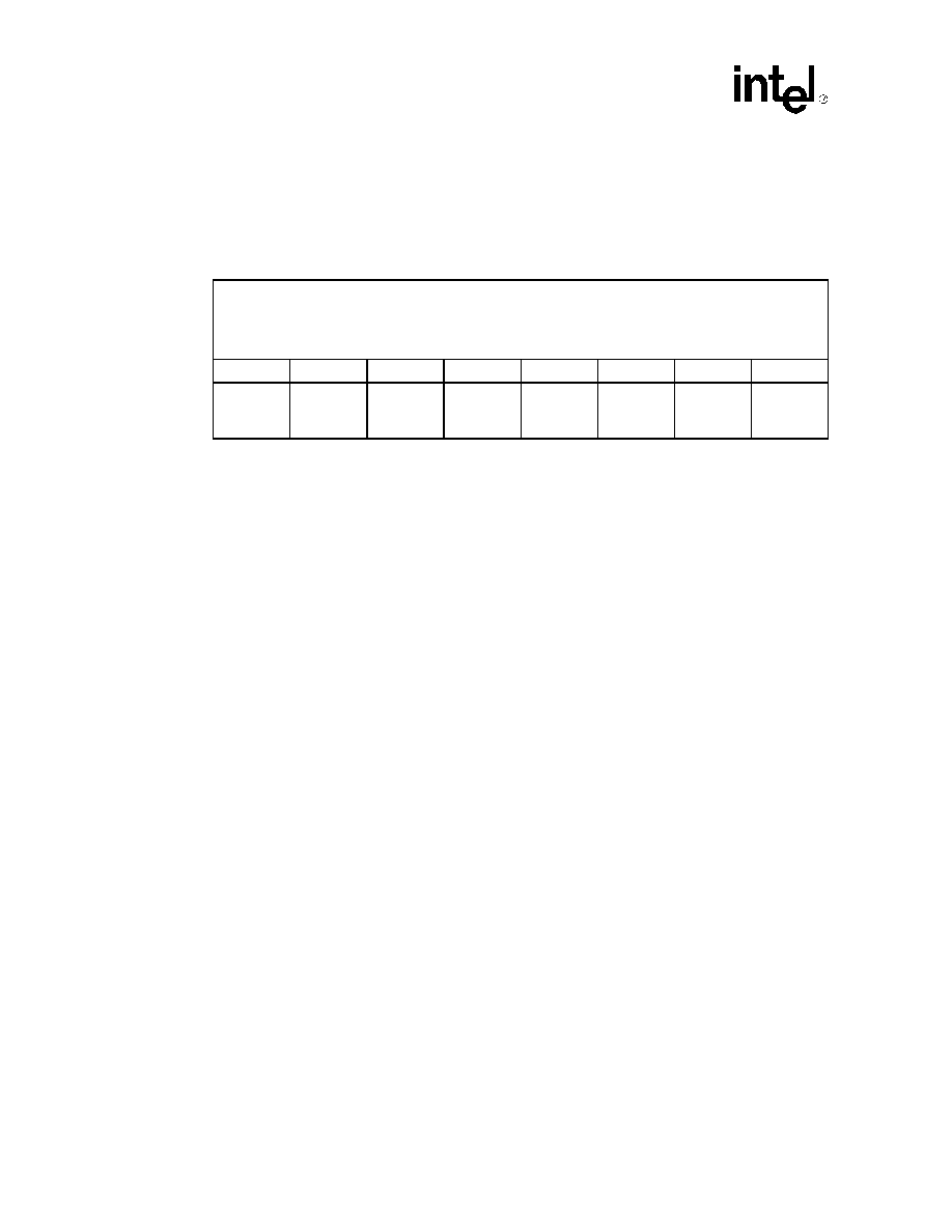
CD1400 -- UXART Serial/Parallel Controller
100
Datasheet
type field. When the command has been executed by the CD1400, it will zero-out the CCR.
Therefore, two consecutive commands must wait for the CCR to be cleared after the first is issued,
before the second is issued.
9.3.2.1
Format 1: Reset Channel Command
Format 1 -- Reset Channel Command
When Bit 7 is set, one of three types of reset operations are initiated, based on the value of the least
significant two bits. Bit 0 sets the type of reset, either channel-only or full-chip, and Bit 1 causes
the FIFO of the selected channel to be flushed.
The two types of reset selected by Bit 0 cause very different results. When Bit 0 is a zero, the reset
command effects only the selected channel. Resetting a channel disables both the receiver and
transmitter, and all FIFOs are flushed (cleared). If Bit 0 is a one, a full-chip reset is initiated. This
reset will have the exact same results as a hardware reset caused by activation of the RESET* Input
Pin. All channels are disabled, all FIFOs are flushed and all Control Registers set to their power-on
reset state. The completion of the reset operation can be detected in the same manner as if a power-
on or hardware reset had occurred; the GFRCR will change from zero to the value of the firmware
revision. It should be noted that, at the beginning of the reset operation, the GFRCR will be
cleared, but it may take some time for this to happen. Host software should wait for the GFRCR to
go to zero, and then wait for it to go non-zero to indicate that the reset operation is complete.
The FTF (Flush Transmit FIFO) command, Bit 1, will cause the transmit FIFO of the selected
channel to be cleared. Any data in the FIFO will be lost.
The encoding of the bits for the reset channel command is:
Register Name: CCR
Hex Address: 05
Register Description: Format 1: Reset Channel Command
Default Value: x'00
Access: Read/Write
Bit 7
Bit 6
Bit 5
Bit 4
Bit 3
Bit 2
Bit 1
Bit 0
Res Chan
0
0
0
0
0
FTF
Type
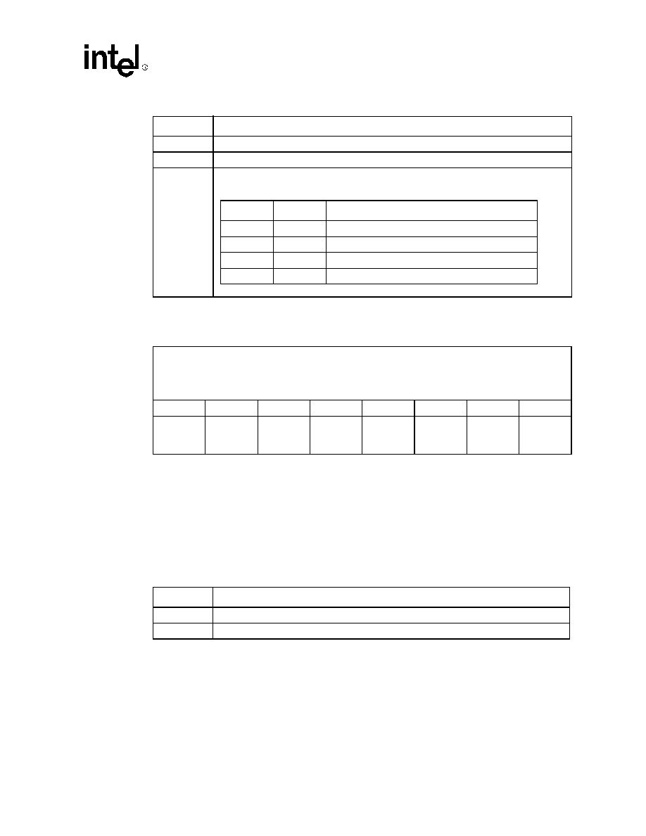
UXART Serial/Parallel Controller -- CD1400
Datasheet
101
9.3.2.2
Format 2: Channel Option Register Change Command
Format 2 -- Channel Option Register Change Command
Bit 6, in combination with any of Bits 1 through 3, will inform the MPU that a change has occurred
in one of the Channel Option Registers, COR1, COR2 and/or COR3, respectively. It is permissible
to indicate that more than one COR has changed.
This command exists so that changes in the COR Registers will be noted by the MPU, allowing it
to update its internal working register, since it stores copies of the COR Registers in its own
shadow registers.
Bit
Description
Bit 7
Must be `1'.
Bits 6:2
Must be `0`.
Bits 1:0
Encoded as:
Register Name: CCR
Hex Address: 05
Register Description: Format 2: Channel Option Register Change Command
Default Value: x'00
Access: Read/Write
Bit 7
Bit 6
Bit 5
Bit 4
Bit 3
Bit 2
Bit 1
Bit 0
0
COR Chg
0
0
COR3
COR2
COR1
0
FTF
Type
Function
0
0
Reset current channel
0
1
Full CD1400 reset
1
0
Flush transmit FIFO of current channel
1
1
Not used
Bit
Description
Bit 7
Must be `0'.
Bit 6
Must be `1'.
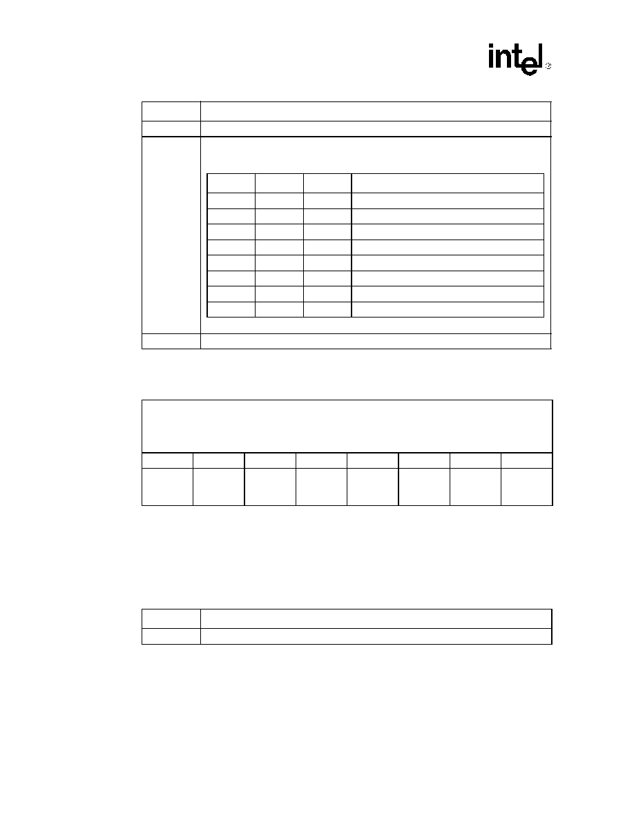
CD1400 -- UXART Serial/Parallel Controller
102
Datasheet
9.3.2.3
Format 3: Send Special Character Command
This command causes one of the pre-programmed characters in the Special Character Registers
(SCHR1, SCHR2, SCHR3, SCHR4) to be sent preemptively. The character sent is selected by the
settings of Bits 2 through 0. `Preemptively' means that the special character will be sent
immediately following the character in the Transmitter Holding Register; it will not wait until the
FIFO empties. Once the special character is sent, transmission of any characters remaining in the
FIFO will proceed normally. Also, CTS is ignored regardless of the setting in COR2 (CtsAE). The
encoding of the bits is:
Bits 5:4
Must be `0'.
Bits 3:1
Encoded as:
Bit 0
Must be `0'.
Register Name: CCR
Hex Address: 05
Register Description: Format 3: Send Special Character Command
Default Value: x'00
Access: Read/Write
Bit 7
Bit 6
Bit 5
Bit 4
Bit 3
Bit 2
Bit 1
Bit 0
0
0
Send SC
0
0
SSPC2
SSPC1
SSPC0
Bit
Description
COR3
COR2
COR1
Encoding
0
0
0 Not
used
0
0
1
COR1 changed.
0
1
0
COR2 changed.
0
1
1
COR1 and COR2 changed.
1
0
0
COR3 changed.
1
0
1
COR3 and COR1 changed.
1
1
0
COR3 and COR2 changed.
1
1
1
COR1, COR2, and COR3 changed.
Bit
Description
Bits 7:6
Must be `0'.
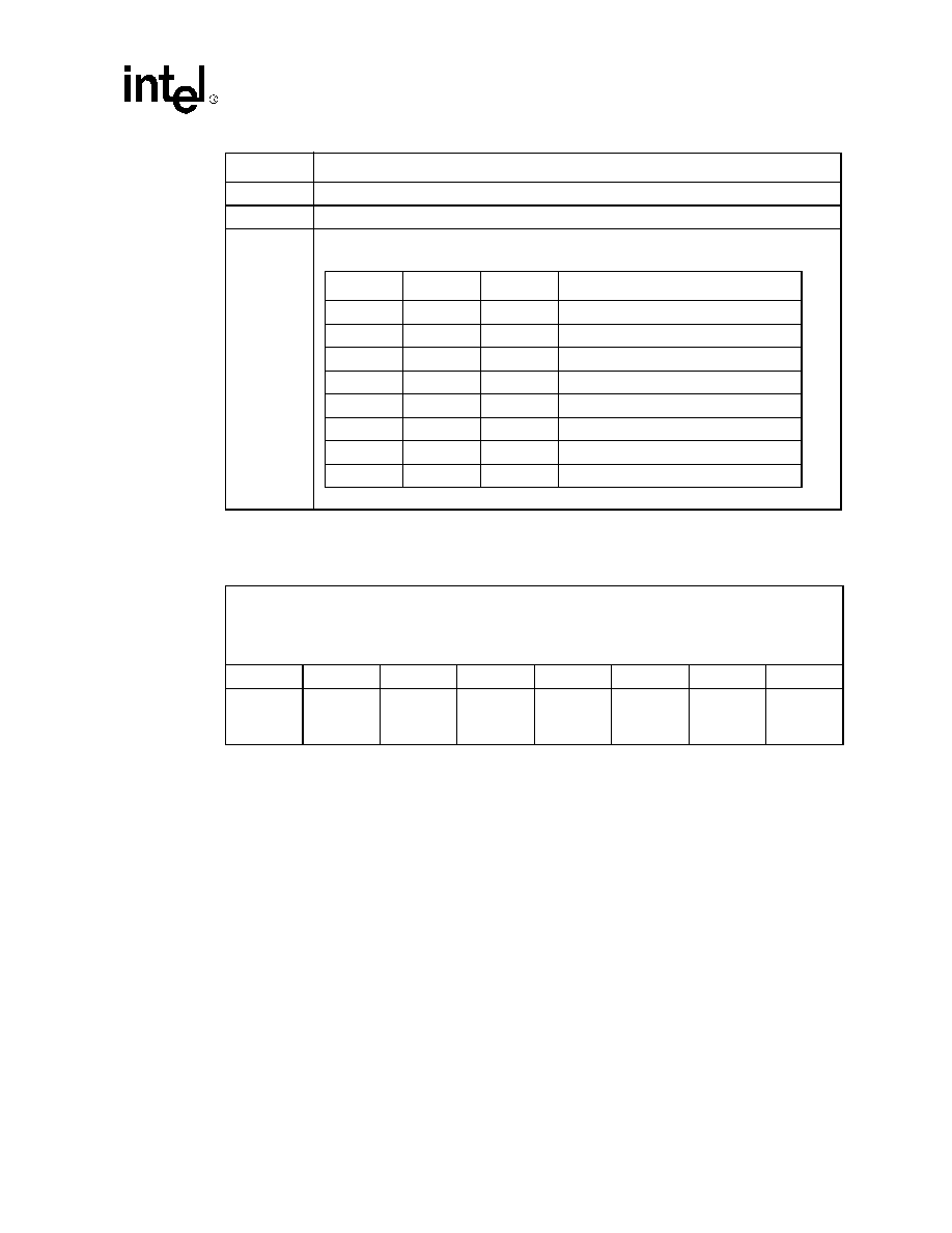
UXART Serial/Parallel Controller -- CD1400
Datasheet
103
9.3.2.4
Format 4: Channel Control Command
This command is used to activate or deactivate the transmitter and/or receiver of the selected
channel, based on the values in Bits 3 through 0. This command must be issued when a channel is
being started for the first time. Once a channel is in use, it can be started and stopped using this
command, though it is more efficient to use of the appropriate SRER Bit in the Interrupt Enable
Register. Multiple control commands can be issued at the same time; for example, both the
transmitter and receiver can be enabled by setting both the XMT EN and RCV EN Bits at the same
time.
Issuing an enable/disable command does not affect any register programming of the selected
channel. It does, however, affect the state of transmit flow-control. Issuing a disable or enable
command to a channel whose transmitter has been flow-controlled by a remote (see the TxIBE Bit
in COR2) will restart transmission and clear the TxFloff Bit in the CCSR. This ability is provided
so that the host can override remote-generated flow control.
Bit 5
Must be `1'.
Bits 4:3
Must be `0'.
Bits 2:0
Encoded as:
Register Name: CCR
Hex Address: 05
Register Description: Format 4: Channel Control Comand
Default Value: x'00
Access: Read/Write
Bit 7
Bit 6
Bit 5
Bit 4
Bit 3
Bit 2
Bit 1
Bit 0
0
0
0
Chan Ctl
XMT EN
XMT DIS
RCV EN
RCV DIS
Bit
Description
SSPC2
SSPC1
SSPCO
Encoding
0
0
0 Not
used
0
0
1
Send special character 1
0
1
0
Send special character 2
0
1
1
Send special character 3
1
0
0
Send special character 4
1
0
1
Not used
1
1
0
Not used
1
1
1
Not used
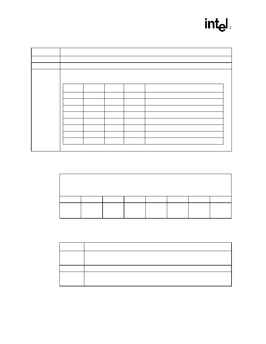
CD1400 -- UXART Serial/Parallel Controller
104
Datasheet
9.3.3
Service Request Enable Register (SRER)
This register is used to enable the conditions that will cause the CD1400 to post a service request
via the SVRR and the SVCREQ* Output Pins. Each of the individual enable bits controls one type
of service request.
Bit
Description
Bits 7:5
Must be `0'.
Bit 4
Must be `1'.
Bits 3:0
Select channel enable/disable activity:
Register Name: SRER
Hex Address: 06
Register Description: Service Request Enable
Default Value: x'00
Access: Read/Write
Bit 7
Bit 6
Bit 5
Bit 4
Bit 3
Bit 2
Bit 1
Bit 0
MdmCh
0
0
RxData
0
TxRdy
TxMpty
NNDT
XMT EN
XMT DIS
RCV EN
RCV DIS
Encoding
0
0
0 1
Disable
receiver
0
0
1
0
Enable receiver
0
1
0
0
Disable transmitter
1
0
0
0
Enable transmitter
0
1
0
0
Disable transmitter and receiver
0
1
1
0
Disable transmitter, enable receiver
1
0
0
1
Enable transmitter, disable receiver
1
0
1
0
Enable transmitter and receiver
Bit
Description
Bit 7
MdmCh: This bit enables the Modem Change Service request. When this bit is a one, any
selected Modem Signal change conditions (as programmed by the MCOR1 and MCOR2
Registers) will cause a Modem Service Request to be posted.
Bits 6:5
Must be `0'.
Bit 4
RxData: The RxData Enable Bit enables the posting of receive service requests when
characters have been received, and either the FIFO has reached the programmed threshold
(as set by COR3), or the receive time-out period has expired.
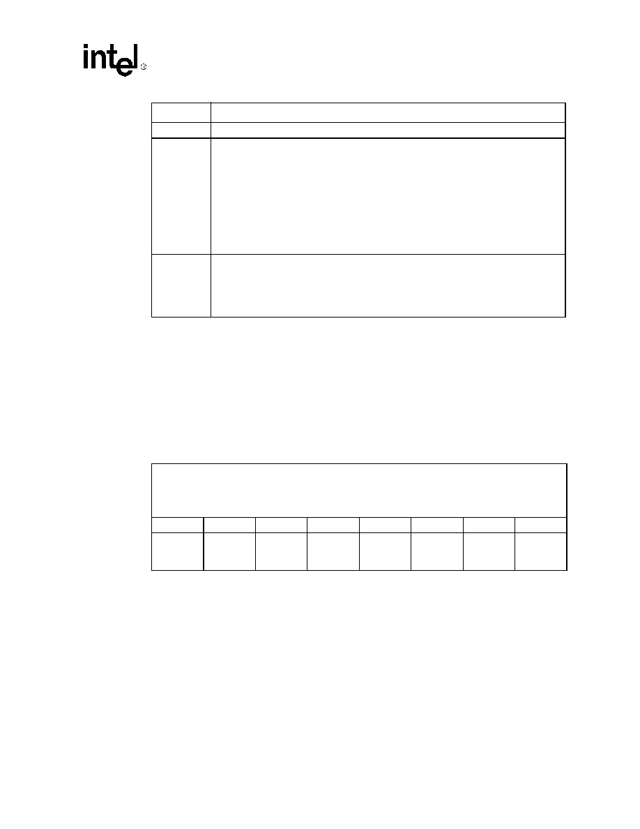
UXART Serial/Parallel Controller -- CD1400
Datasheet
105
9.4
Channel Option Registers
The following five Channel Option Registers are used to control many aspects of CD1400 channel
operation and enable special character processing features. COR4 and COR5 are used specifically
for enabling the UNIX line discipline character-handling functions.
9.4.1
Channel Option Register 1 (COR1)
Bit 3
Must be `0'.
Bits 2:1
TxRdy and TxMpty: The transmitter can be enabled to post service requests on one of two
conditions: either the FIFO is empty, or the Transmitter Shift Register is empty.
The TxRdy Bit enables the service request on the condition that the FIFO is empty. In this
case, there are still two characters available for transmission before the transmitter underruns,
one in the Shift Register and one in the Holding Register.
The TxMpty Bit enables the service request on the condition that the Shift Register is empty.
The transmitter will underrun in this situation due to the latency that will be experienced
between the time the service request is posted, and the time that the host is able to load the
FIFO. Under normal operating conditions, this bit will be set and the TxRdy reset, when there
is no more data to be transmitted, and the host wants to know when the last character has
been sent before disabling the transmitter.
Bit 0
NNDT: The No New Data Time-out Enable Bit activates the optional exception service request
when all data has been removed from the FIFO, and no new data has arrived after a pre-
programmed delay period set by the value in the Receive Time-out Period Register (RTPR).
The LIVR (or RIVR) will indicate a receive exception in the IT2-IT0 Vector Bits. There will be
no data associated with this exception service request. A status bit in the RDSR (Bit 7) will
indicate that the service request is for an NNDT condition.
Bit
Description
Register Name: COR1
Hex Address: 08
Register Description: Channel Option Register 1
Default Value: x'00
Access: Read/Write
Bit 7
Bit 6
Bit 5
Bit 4
Bit 3
Bit 2
Bit 1
Bit 0
Parity
ParM1
ParM0
Ignore
Stop1
Stop0
ChL1
ChL0
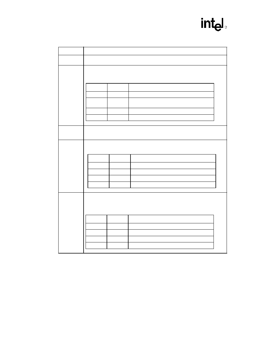
CD1400 -- UXART Serial/Parallel Controller
106
Datasheet
Bit
Description
Bit 7
Parity Type: This bit selects the type of parity that is generated and checked if parity is
enabled. A `1' selects odd parity and a `0' selects even parity.
Bits 6:5
Parity Mode 1 and Parity Mode 0: The Parity Mode Bits define the parity operation for both
the transmitter and receiver. The encoding is:
Bit 4
Ignore Parity: If this bit is set, the CD1400 will ignore the parity on all incoming characters,
thus no receive exception service requests will be generated if the parity is in error. If the bit is
cleared, parity is evaluated.
Bits 3:2
Stop Bit Length: These two bits set the length, in bit times, of the stop bit for each character.
Bits 1:0
Character Length: ChL1 and ChL0 select the length of each character, in number of bits.
The D1400 receives and transmits the same length character, on a given channel, in the
range of five to eight bits.
ParM1
ParM0
Function
0
0
No parity
0
1
Force parity (odd parity = force 1, even parity = force
0)
1
0
Normal parity
1
1
Not used
Stop1
Stop0
Number of Stop Bits
0
0
1 Stop Bit
0
1
1.5 Stop Bits
1
0
2 Stop Bits
1
1
Not used
ChL1
ChL0
Character Length
0
0
5 bits
0
1
6 bits
1
0
7 bits
1
1
8 bits
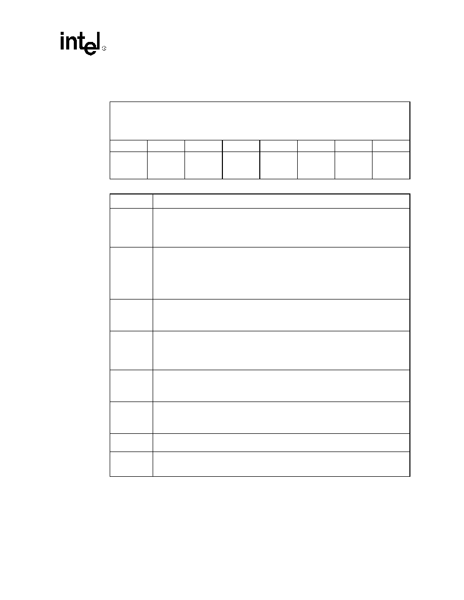
UXART Serial/Parallel Controller -- CD1400
Datasheet
107
9.4.2
Channel Option Register 2 (COR2)
Register Name: COR2
Hex Address: 09
Register Description: Channel Option Register 2
Default Value: x'00
Access: Read/Write
Bit 7
Bit 6
Bit 5
Bit 4
Bit 3
Bit 2
Bit 1
Bit 0
IXM
TxIBE
ETC
LLM
RLM
RtsAO
CtsAE
DsrAE
Bit
Description
Bit 7
Implied X-ON Mode: The IXM Bit enables the automatic resumption of character
transmission upon the reception of any character. This bit only has meaning if the transmitter
is in Automatic In-band Flow Control Mode as programmed by the TxIBE Control Bit. If this bit
is reset and TxIBE is enabled, the reception of any character will restart character
transmission.
Bit 6
Enable Automatic In-band Transmit Flow Control: This bit enables the CD1400 capability
to examine error-free incoming characters looking for an X-OFF character (as programmed by
SCHR2), if the special character match function is enabled (COR3, Bit 4). If a match occurs,
transmission will cease after the current characters in the Transmitter Shift Register and
Transmitter Holding Register have been sent. Transmission will resume when an X-ON
character (or any character, depending on the value of the IXM Bit) is received or if a channel-
enable command is issued via the CCR.
Bit 5
Embedded Transmit Command Enable: If the ETC Bit is set, the CD1400 will examine
characters in the transmit FIFO. If an embedded command is detected, it will be processed.
See the embedded-transmit command description in
"Functional Description" on page 29
for
details of valid commands.
Bit 4
Local Loopback Mode: The LLM Bit enables local loopback of the channel. This mode is
generally used during system diagnostics. If this bit is set, the transmitter is internally `looped'
back to the receiver. The TxD Pin is set to the marking state. Data sent will be immediately
received by the receiver. No data will appear on the TxD Pin, and data on the RxD Pin will be
ignored.
Bit 3
Remote Loopback Mode: Remote loopback allows a remote system to test its serial data
stream. If this function is enabled, the CD1400 internally connects its receiver to the
transmitter. Any data received is immediately echoed back. This mode is enabled by setting
the RLM Bit and disabled by clearing the bit.
Bit 2
Request To Send Automatic Output: The CD1400 can automatically assert RTS when a
channel is enabled (via transmit/receive enable command in the CCR) and there is data in the
FIFO. When the channel is disabled or there is no more data to send (FIFO, Holding Register
and Shift Register), RTS* will be negated. Setting RtsAO enables the function.
Bit 1
Clear To Send Automatic Enable: This bit enables the CTS* Input to control transmitter
operation. If CtsAE is set, and CTS* is not asserted, character transmission will not proceed.
Bit 0
Data Set Ready Automatic Enable: DsrAE allows the DSR* Input to control receiver
operation. Setting DsrAE enables the function. When enabled, if DSR* is deasserted, the
CD1400 discards all received characters.
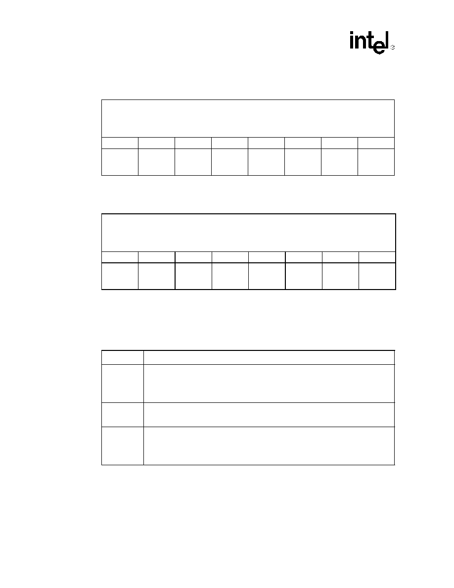
CD1400 -- UXART Serial/Parallel Controller
108
Datasheet
9.4.3
Channel Option Register 3 (COR3) Serial Format
9.4.4
Channel Option Register 3 (COR3) Parallel Format
COR3 for Channel 0 has two formats, one for serial and one for parallel. Channels 3-1 have only
the serial format. Both formats are described as follows:
Channel Option Register 3 ≠ Serial
Register Name: COR3
Hex Address: 0A
Register Description: Channel Option Register 3 -- Serial
Default Value: x'00
Access: Read/Write
Bit 7
Bit 6
Bit 5
Bit 4
Bit 3
Bit 2
Bit 1
Bit 0
SCDRNG
SCD34
FCT
SCD12
RxTh3
RxTh2
RxTh1
RxTh0
Register Name: COR3
Hex Address: 0A
Register Description: Channel Option Register 3 -- Parallel
Default Value: x'00
Access: Read/Write
Bit 7
Bit 6
Bit 5
Bit 4
Bit 3
Bit 2
Bit 1
Bit 0
0
0
0
RxTh4
RxTh3
RxTh2
RxTh1
RxTh0
Bit
Description
Bit 7
Special Character Detect Range: This bit enables range checking on received characters. If
the character falls between a lower range set by the value stored in the SCRL Register and an
upper range set by the value stored in the SCRH Register, inclusive, a receive exception
service request will be posted with the status indicating a range detect (RDSR Bits SCDet2-
SCDet0 = 111).
Bit 6
Enable Special Character Detect on SCHR4-SCHR3: This bit controls whether or not the
CD1400 performs comparison on received characters against the values stored in Registers
SCHR4 and SCHR3. The comparison is enabled by a `1' in this location.
Bit 5
Flow Control Transparency: The FCT Bit enables and disables transparent response to flow
control characters received by the CD1400. If FCT is set, received XON and XOFF characters
will not be placed in the FIFO for the host. If in-band flow control is enabled, the characters will
be acted upon. If FCT is not set, flow control characters will be acted upon, placed in the
receive FIFO, and the host will be notified via a receive exception service request.
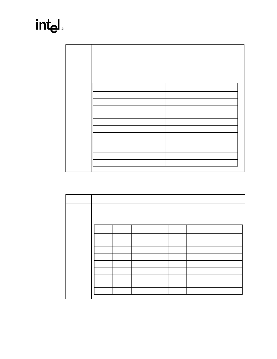
UXART Serial/Parallel Controller -- CD1400
Datasheet
109
Channel Option Register 3 ≠ Parallel
Bit 4
Enable Special Character Detect on SCHR2-SCHR1: This bit controls whether or not the
CD1400 compares received characters with the values stored in Registers SCHR2 and
SCHR1. A `1' enables compare. This bit must be set to enable automatic in-band flow control.
Bits 3:0
Receive FIFO Threshold
Bit
Description (Continued)
RxTh3
RxTh2
RxTh1
RxTh0
Receiver FIFO Threshold
0
0
0
0
Not used
0
0
0
1
1 Character
0
0
1
0
2 Characters
0
0
1
1
3 Characters
∑
∑
∑
∑
∑
∑
∑
∑
∑
∑
1
0
1
1
11 Characters
1
1
0
0
12 Characters
1
1
0
1
Not used
1
1
1
0
Not used
1
1
1
1
Not used
Bit
Description
Bits 7:5
Not used
Bits 4:0
Receive FIFO Threshold
RxTh4
RxTh3
RxTh2
RxTh1
RxTh0
Receiver FIFO Threshold
0
0
0
0
0
Not used
0
0
0
0
1
1 Character
0
0
0
1
0
2 Characters
∑
∑
∑
∑
∑
∑
∑
∑
∑
∑
∑
∑
∑
∑
∑
∑
∑
∑
1
1
1
0
1
29 Characters
1
1
1
1
0
30 Characters
1
1
1
1
1
Not used
CD1400 -- UXART Serial/Parallel Controller
110
Datasheet
9.4.5
Channel Option Register 4 (COR4)
Register Name: COR4
Hex Address: 1E
Register Description: Channel Option Register 4
Default Value: x'00
Access: Read/Write
Bit 7
Bit 6
Bit 5
Bit 4
Bit 3
Bit 2
Bit 1
Bit 0
IGNCR
ICRNL
INLCR
IGNBRK
-BRKINT
PEH[2]
PEH[1]
PEH[0]
Bit
Description
Bits 7:5
Carriage Return (CR) and New Line (NL) Processing
These three bits define the manner in which the CD1400 will process received CR and NL characters (x'0D
and x'0A). The table below shows the actions performed:
IGNCR
ICRNL
INLCR
Action
0
0
0
No action
0
0
1
Received NL changed to CR
0
1
0
Received CR changed to NL
0
1
1
Received CR changed to NL; NL changed to CR
1
0
0
Received CR discarded
1
0
1
Received CR discarded; NL changed to CR
1
1
0
Received CR discarded
1
1
1
Received CR discarded; NL changed to CR
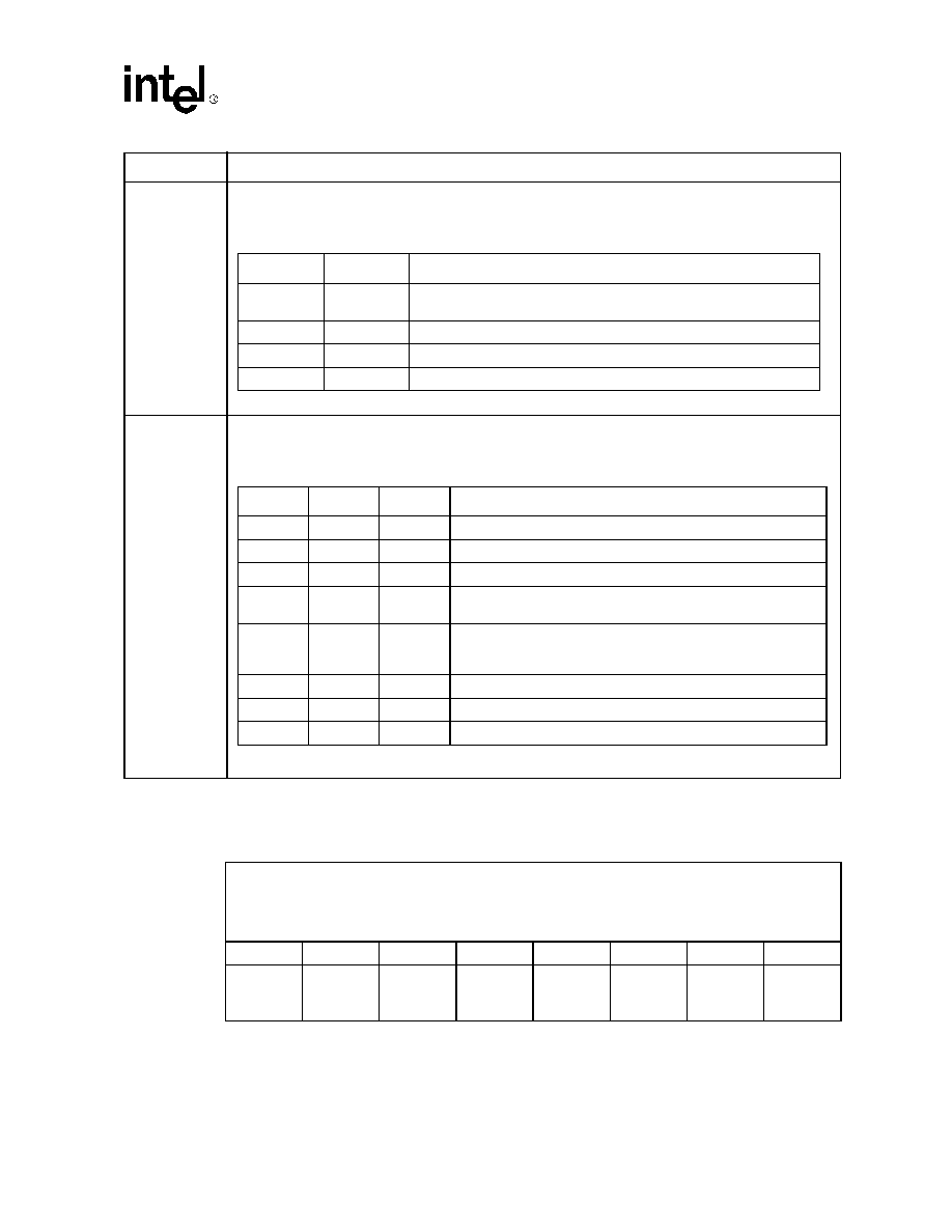
UXART Serial/Parallel Controller -- CD1400
Datasheet
111
9.4.6
Channel Option Register 5 (COR5)
Bits 4:3
Break Processing
The CD1400 can handle received break characters in three ways:
Bits 2:0
Parity (P), Framing (F) and Overrun (O) Error Special Processing
As with break characters, if enabled, the CD1400 can treat errored characters in several different ways:
Register Name: COR5
Hex Address: 1F
Register Description: Channel Option Register 5
Default Value: x'00
Access: Read/Write
Bit 7
Bit 6
Bit 5
Bit 4
Bit 3
Bit
Bit 1
Bit 0
ISTRIP
LNE
CMOE
0
0
EBD
ONLCR
OCRNL
Bit
Description (Continued)
IGNBRK
-BRKINT
Break Action
0
0
Received break generates an exception service request. End-of-Break
also generates an exception service request if EBD is enabled in COR5.
0
1
Received break treated as a good NULL character.
1
0
Not used.
1
1
Received break discarded.
PEH[2]
PEH[1]
PEH[0]
Action
0
0
0
Received P/F/O errored characters treated as exception data.
0
0
1
Received P/F/O errored characters treated as good data.
0
1
0
Received P/F/O errored characters discarded.
0
1
1
Received P/F/O errored characters replaced with good NULL
characters.
1
0
0
Received P/F/O errored characters are replaced with the two
character sequence x'FF-NULL-character. Good x'FF characters
are replaced with the two character sequence x'FF-x'FF.
1
0
1
Not used.
1
1
0
Not used.
1
1
1
Not used.
CD1400 -- UXART Serial/Parallel Controller
112
Datasheet
9.4.7
Channel Control Status Register (CCSR) Serial Format
9.4.8
Channel Control Status Register (CCSR) Parallel Format
Bit
Description
Bit 7
ISTRIP: The ISTRIP Bit enables stripping of the most significant bit (Bit 7) on all received
characters. A `1' in this position enables the function.
Bit 6
LNext Enable: When this bit is set, characters following an LNext Character (as programmed
by the LNC Register) will not be processed as a special character.
Bit 5
Character Matching on Error: If this bit is set, character matching will occur on both good
and errored characters. If the bit is cleared, matching will occur on good characters only.
Bits 4:3
Must be `0'.
Bit 2
End of Break Detect: If this bit is set, the CD1400 will, after detecting and reporting a line-
break condition, search for the end of a break and report it via an exception service request
with the End of Break status in the RDSR (see the RDSR description).
Bits 1:0
Carriage Return (CR) and New Line (NL) Processing ≠ Transmit
These two bits define actions, if any, taken on characters in the transmit data stream.
Register Name: CCSR
Hex Address: 0B
Register Description: Channel Control Status -- Serial
Default Value: x'00
Access: Read/Write
Bit 7
Bit 6
Bit 5
Bit 4
Bit 3
Bit 2
Bit 1
Bit 0
RxEN
RxFloff
RxFlon
0
TxEN
TxFloff
TxFlon
0
Register Name: CCSR
Hex Address: 0B
Register Description: Channel Control Status -- Parallel
Default Value: x'00
Access: Read/Write
Bit 7
Bit 6
Bit 5
Bit 4
Bit 3
Bit 2
Bit 1
Bit 0
RxEN
0
0
0
TxEN
0
0
0
ONLCR
OCRNL
Action
0
0
No action
0
1
Transmit CR changed to NL
1
0
Transmit NL changed to CRNL
1
1
Transmit CR changed to NL, NL changed to CRNL
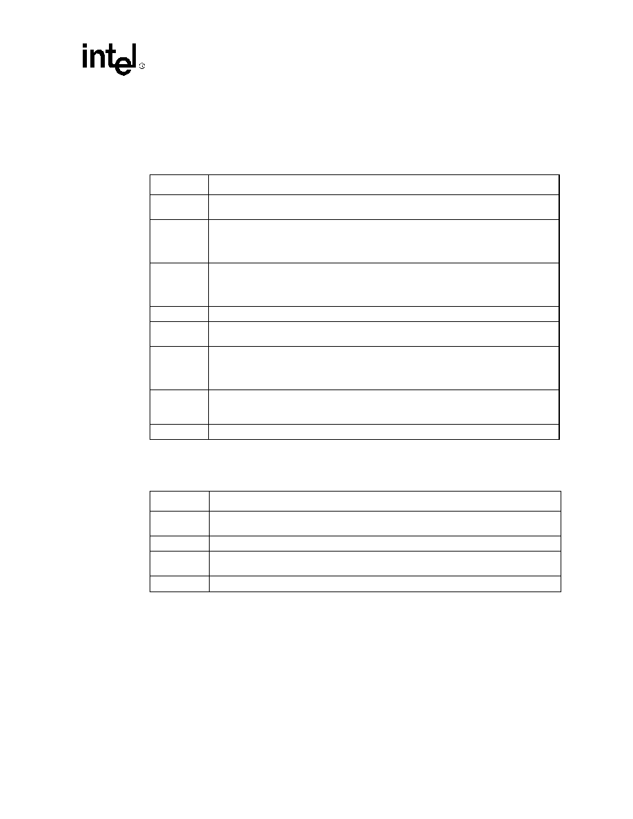
UXART Serial/Parallel Controller -- CD1400
Datasheet
113
The CCSR provides current status of the selected channel. The CCSR for Channel 0 has two
formats, one for serial operation and another for parallel operation.
Channel Control Status Register ≠ Serial
Channel Control Status Register ≠ Parallel
Bit
Description
Bit 7
Receiver Enabled: The RxEN Bit is set when the receiver is enabled and cleared when it is
disabled.
Bit 6
Receiver Flow Off: This bit indicates that the receiver has requested the remote to stop
transmitting through the use of a send XOFF character via a send special character two
command in the CCR. The bit will be cleared when a Send Special Character 1 (XON)
command is issued; the channel is either enabled or disabled or the channel is reset.
Bit 5
Receiver Flow On: When a send special character one (XON) command is issued via the
CCR, this bit will be set. It will be cleared when one of three events has occurred: the first non-
flow control character is received, the receiver is either enabled or disabled or the channel is
reset.
Bit 4
Not used, will return `0' when read.
Bit 3
Transmitter Enabled: This bit is set when the transmitter is enabled and cleared when it is
disabled.
Bit 2
Transmitter Flow Off: This bit indicates that the CD1400 has been requested to stop
transmission by the remote (received in-band flow control character XOFF). The bit is cleared
when the CD1400 requested to restart transmission (receives an XON character), the channel
is either enabled or disabled or the channel is reset.
Bit 1
Transmitter Flow On: TxFlon is set when the CD1400 has been requested to restart
transmission (received an XON character). It is reset when transmission actually begins, when
the channel is either enabled or disabled or when the channel is reset.
Bit 0
Not used, will return `0' when read.
Bit
Description
Bit 7
Receiver Enabled: The RxEN Bit is set when the receiver is enabled and cleared when it is
disabled.
Bits 6:4
Not used, will return `0' when read.
Bit 3
Transmitter Enabled: This bit is set when the transmitter is enabled and cleared when it is
disabled.
Bits 2:0
Not used, will return `0' when read.
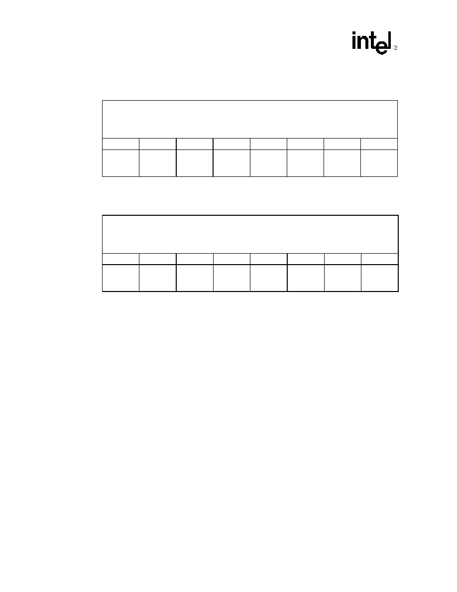
CD1400 -- UXART Serial/Parallel Controller
114
Datasheet
9.4.9
Received Data Count Register (RDCR) Serial Format
9.4.10
Received Data Count Register (RDCR) Parallel Format
The RDCR indicates the number of good characters currently in the received data FIFO. Host
software can use this value as a loop counter when taking characters out of the FIFO. The value in
this register is only valid during the context of a service request acknowledge. At other times, it
may or may not provide a true indication of the number of characters in the FIFO.
The register has two formats for Channel 0, one for serial and one for parallel. Channels 1-3 have
only the serial format.
Register Name: RDCR
Hex Address: 0E
Register Description: Receive Data Count -- Serial
Default Value: x'00
Access: Read only
Bit 7
Bit 6
Bit 5
Bit 4
Bit 3
Bit 2
Bit 1
Bit 0
0
0
0
0
CT3
CT2
CT1
CT0
Register Name: RDCR
Hex Address: 0E
Register Description: Receive Data Count -- Parallel
Default Value: x'00
Access: Read only
Bit 7
Bit 6
Bit 5
Bit 4
Bit 3
Bit 2
Bit 1
Bit 0
0
0
0
CT4
CT3
CT2
CT1
CT0
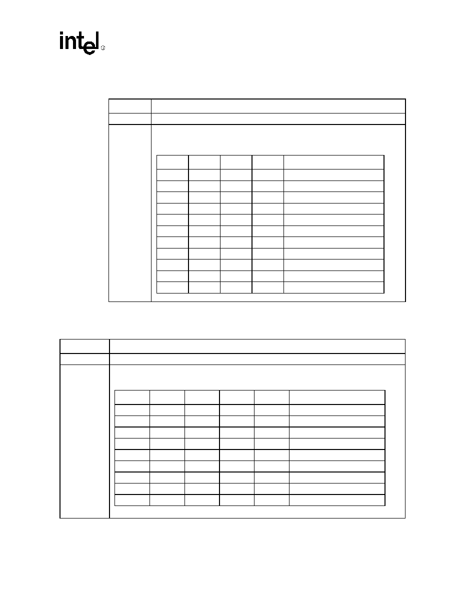
UXART Serial/Parallel Controller -- CD1400
Datasheet
115
Received Data Count Register ≠ Serial
Received Data Count Register ≠ Parallel
Bit
Description
Bits 7:4
Always `0'
Bits 3:0
Character count CT3-CT0
CT3
CT2
CT1
CT0
Number of characters in FIFO
0
0
0
0
Not used
0
0
0
1
1 Character
0
0
1
0
2 Characters
∑
∑
∑
∑
∑
∑
∑
∑
∑
∑
∑
∑
∑
∑
∑
1
0
1
1
11 Characters
1
1
0
0
12 Characters
1
1
0
1
Not used
1
1
1
0
Not used
1
1
1
1
Not used
Bit
Description
Bits 7:5
Always `0'
Bits 4:0
Character count CT4-CT0
CT4
CT3
CT2
CT1
CT0
Number of Characters in FIFO
0
0
0
0
0
Not used
0
0
0
0
1
1 Character
0
0
0
1
0
2 Characters
∑
∑
∑
∑
∑
∑
∑
∑
∑
∑
∑
∑
∑
∑
∑
∑
∑
∑
1
1
1
0
1
29 Characters
1
1
1
1
0
30 Characters
1
1
1
1
1
Not used
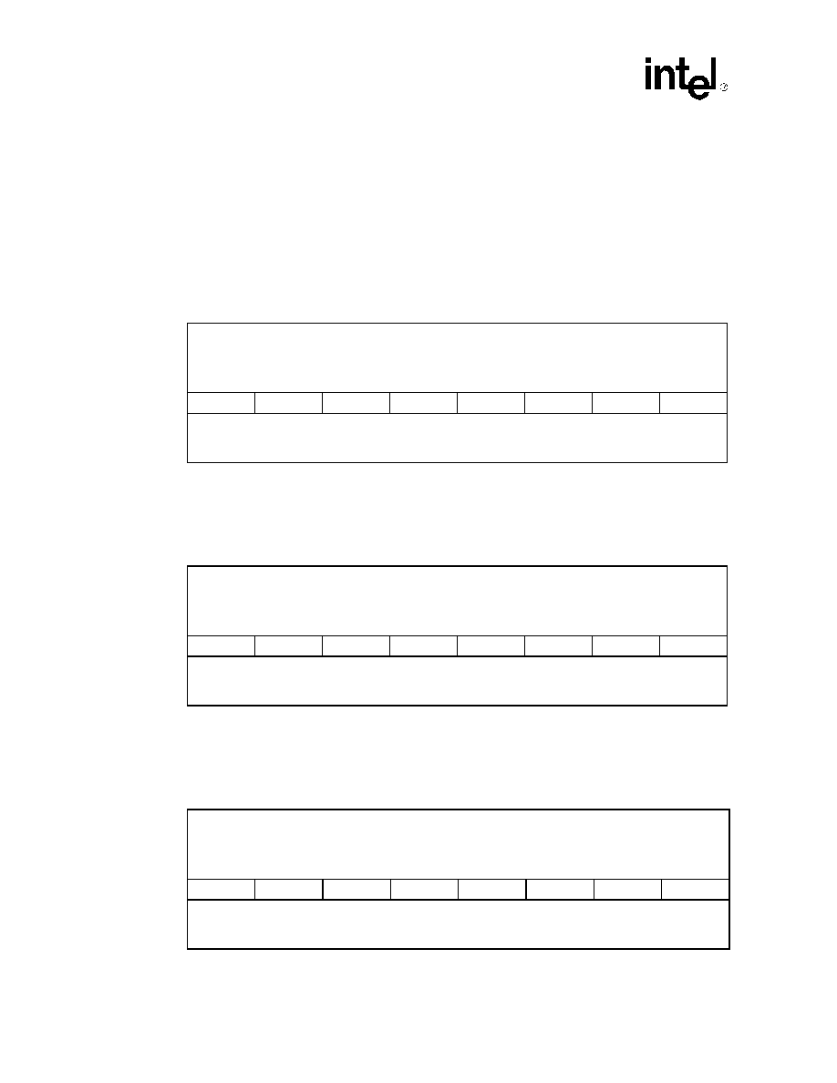
CD1400 -- UXART Serial/Parallel Controller
116
Datasheet
9.5
Special Character Registers
The four Special Character Registers, SCHR4-SCHR1, hold the character patterns that are used for
various character matching and flow control functions. Each 8-bit character is right-justified, that
is, comparison takes place from right to left, and all bits are compared. Any unused bits must be
zero. SCHR1 and SCHR2 serve the additional function of defining the XON and XOFF characters,
respectively, used for in-band flow control.
9.5.1
Special Character Register 1 (SCHR1)
SCHR1 defines the XON Character
9.5.2
Special Character Register 2 (SCHR2)
SCHR2 defines the XOFF Character
9.5.3
Special Character Register 3 (SCHR3)
Register Name: SCHR1
Hex Address: 1A
Register Description: Special Character Register 1
Default Value: x'00
Access: Read/Write
Bit 7
Bit 6
Bit 5
Bit 4
Bit 3
Bit 2
Bit 1
Bit 0
Special Character 1
Register Name: SCHR2
Hex Address: 1B
Register Description: Special Character Registr 2
Default Value: x'00
Access: Read/Write
Bit 7
Bit 6
Bit 5
Bit 4
Bit 3
Bit 2
Bit 1
Bit 0
Special Character 2
Register Name: SCHR3
Hex Address: 1C
Register Description: Special Character Register 3
Default Value: x'00
Access: Read/Write
Bit 7
Bit 6
Bit 5
Bit 4
Bit 3
Bit 2
Bit 1
Bit 0
Special Character 3
UXART Serial/Parallel Controller -- CD1400
Datasheet
117
9.5.4
Special Character Register 4 (SCHR4)
Received Character Range Detection
If enabled (through Bit 7 of COR3), the CD1400 will check received characters to see if they fall
within a range of values. Two registers set the range: SCRL and SCRH. Range checking occurs
inclusive of the values programmed into these registers. If a received character is determined to be
within the range, a special character detect exception service request will be posted. Bits 6-4 of the
RDSR will indicate a range detect by being set to 111. It should be noted that this range checking is
performed in addition to normal special character detection on SCHR4-SCHR1.
9.5.5
Special Character Range Low (SCRL)
SCRL set the lower inclusive value for range detection.
9.5.6
Special Character Range High (SCRH)
SCRH sets the upper inclusive value for range detection.
Register Name: SCHR4
Hex Address: 1D
Register Description: Special Character Register 4
Default Value: x'00
Access: Read/Write
Bit 7
Bit 6
Bit 5
Bit 4
Bit 3
Bit 2
Bit 1
Bit 0
Special Character 4
Register Name: SCRL
Hex Address: 22
Register Description: Special Character Range Low
Default Value: x'00
Access: Read/Write
Bit 7
Bit 6
Bit 5
Bit 4
Bit 3
Bit 2
Bit 1
Bit 0
Character Range Low
Register Name: SCRH
Hex Address: 23
Register Description: Special Character Range High
Default Value: x'00
Access: Read/Write
Bit 7
Bit 6
Bit 5
Bit 4
Bit 3
Bit 2
Bit 1
Bit 0
Character Range High
CD1400 -- UXART Serial/Parallel Controller
118
Datasheet
9.5.7
LNext Character (LNC)
This register defines the LNext Character. If the LNext function is enabled (Bit 6 of COR5), the
CD1400 will examine received characters and compare them against this value. If a match occurs,
this character and the following will be placed in the FIFO without any special processing. In
effect, the LNext function causes the CD1400 to ignore characters with special meaning, such as
flow control characters. There are two exceptions. If the character following the LNext Character is
either a break or an errored character, LNext will be placed in the FIFO, and the following
character will be treated as it normally would for these error conditions.
9.6
Modem Change Option Registers
The CD1400 has two registers that control its response to changes on the Modem Input Pins. It can
be programmed to respond to the low-to-high transition, the high-to-low transition or both. In
addition, the threshold at which the DTR Signal will be negated can be set by the DTRth3-DTRth0
Bits in MCOR1.
9.6.1
Modem Change Option Register 1 (MCOR1) Serial Format
Register Name: LNC
Hex Address: 24
Register Description: LNext Character
Default Value: x'00
Access: Read/Write
Bit 7
Bit 6
Bit 5
Bit 4
Bit 3
Bit 2
Bit 1
Bit 0
LNext Character
Register Name: MCOR1
Hex Address: 15
Register Description: Modem Change Option Register 1 -- Serial
Default Value: x'00
Access: Read/Write
7Bit
Bit 6
Bit 5
Bit 4
Bit 3
Bit 2
Bit 1
Bit 0
DSRzd
CTSzd
RIzd
CDzd
DTRth3
DTRth2
DTRth1
DTRth0
UXART Serial/Parallel Controller -- CD1400
Datasheet
119
9.6.2
Modem Change Option Register 1 (MCOR1) Parallel Format
Channel 0 has two formats for MCOR1: one applies when the channel is in Serial Mode and the
other applies in Parallel Mode, as set by the GCR. Channels 3-1 have only the Serial Mode format.
Modem Change Option Register 1 ≠ Serial
Register Name: MCOR1
Hex Address: 15
Register Description: Modem Change Option Register 1 -- Parallel
Default Value: x'00
Access: Read/Write
Bit 7
Bit 6
Bit 5
Bit 4
Bit 3
Bit 2
Bit 1
Bit 0
PBUSYzd
PSLCTzd
RIzdPPEzd
PERRORzd
0
0
0
0
Bit
Description
Bit 7
DSRzd
Bit 6
CTSzd
Bit 5
RIzd
Bit 4
CDzd: Each of these bits controls its corresponding input pin. If the bit is set, the function is
enabled and transitions from one-to-zero will generate an SVCREQM* service request.
Bits 3:0
DTRth3-DTRth0: These bits form a binary value that determines when the DTR Output will be
negated, based on the number of characters in the receive FIFO. When the FIFO holds more
characters than this value, DTR will be negated, informing the remote that it should stop
transmission. This value must be set to a value numerically larger than the value set for the
receive FIFO threshold in COR3.
DTRth3
DTRth2
DTRth1
DTRth0
Number of characters in FIFO
0
0
0
0
Automatic DTR Mode disabled
0
0
0
1
1 Character
0
0
1
0
2 Characters
∑
∑
∑
∑
∑
∑
∑
∑
∑
∑
∑
∑
∑
∑
∑
1
0
1
1
11 Characters
1
1
0
0
12 Characters
1
1
0
1
Not used
1
1
1
0
Not used
1
1
1
1
Not used
CD1400 -- UXART Serial/Parallel Controller
120
Datasheet
Modem Change Option Register 1 ≠ Parallel
9.6.3
Modem Change Option Register 2 (MCOR2) Serial Format
9.6.4
Modem Change Option Register 2 (MCOR2) Parallel Format
Channel 0 has two formats for MCOR2: one applies when the channel is in Serial Mode and the
other applies in Parallel Mode, as set by the GCR. Channels 3-1 have only the Serial Mode format.
Bit Description
Bit 7
PBUSYzd: When BUSY in an input (Parallel Transmit Mode).
Bit 6
PSLCTzd
Bit 5
PPEzd
Bit 4
PERRORzd: Effectively, these four bits are identical to the equivalent bits in the serial format
above. The only difference is in the signal names. These inputs are renamed for convenience
in working with the register when Channel 0 is programmed to be a parallel port. Setting any
of these bits will enable the detection of a one-to-`0' transition on the corresponding input.
Bits 3:0
Not used; must be `0'.
Register Name: MCOR2
Hex Address: 16
Register Description: Modem Change Option Register 2 -- Serial
Default Value: x'00
Access: Read/Write
Bit 7
Bit 6
Bit 5
Bit 4
Bit 3
Bit 2
Bit 1
Bit 0
DSRod
CTSod
RIod
CDod
0
0
0
0
Register Name: MCOR2
Hex Address: 16
Register Description: Modem Change Option Register 2 -- Parallel
Default Value: x'00
Access: Read/Write
Bit 7
Bit 6
Bit 5
Bit 4
Bit 3
Bit 2
Bit 1
Bit 0
PBUSYod
PSLCTod
PPEod
PERRORod
0
0
0
0
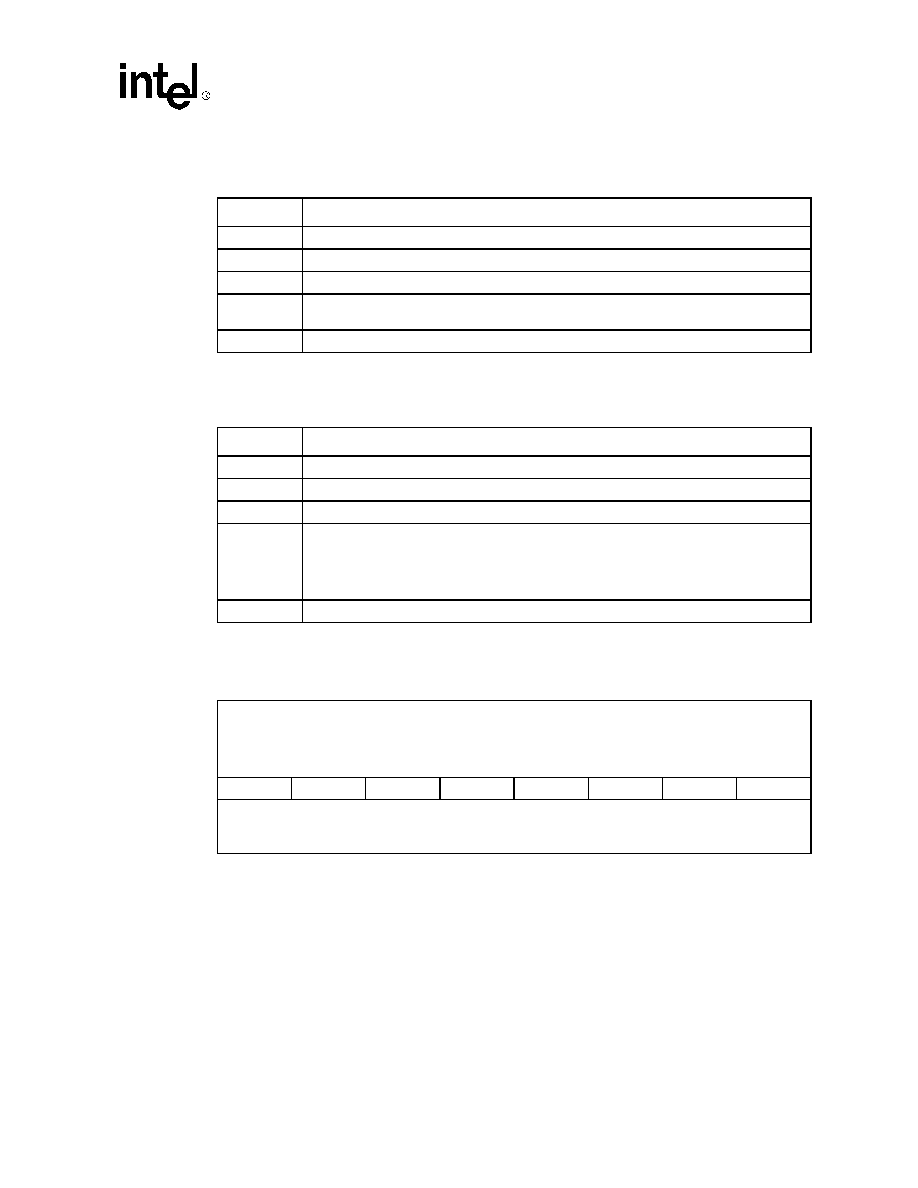
UXART Serial/Parallel Controller -- CD1400
Datasheet
121
Modem Change Option Register 2 ≠ Serial
Modem Change Option Register 2 ≠ Parallel
9.6.5
Receive Time-out Period Register (RTPR)
The RTPR determines the time period that will be used for the No New Data Time-out (NNDT)
and the stale data time-out. The Time-out Counter is loaded from this register whenever a new
character is placed in, or the last character is removed from, the receive FIFO. The counter is
decremented on each `tick' of the prescaler counter (PPR). A service request will be generated if
the count reaches zero; either an NNDT if the FIFO is empty and the NNDT is enabled, or a good
data service request if there is data in the FIFO, but the time-out period has expired before the FIFO
reaches the programmed threshold (the data has become stale).
Bit
Description
Bit 7
DSRod
Bit 6
CTSod
Bit 5
RIod
Bit 4
CDod: Each of these bits controls its corresponding input pin. If the bit is set, the function is
enabled and transitions from zero-to-one will generate an SVCREQM* service request.
Bits 3:0
These bits are not used and must be programmed to `0'.
Bit
Description
Bit 7
PBUSYod: When BUSY in an input (Parallel Transmit Mode).
Bit 6
PSLCTod
Bit 5
PPEod
Bit 4
PERRORod: Effectively, these four bits are identical to the equivalent bits in the serial format.
The only difference is in the signal names. As with the parallel format of MCOR1, these inputs
are renamed for convenience in working with the register when Channel 0 is programmed to
be a parallel port. Setting any of these bits will enable the detection of a zero-to-one transition
on the corresponding input.
Bits 3:0
Not used; must be programmed to `0'.
Register Name: RTPR
Hex Address: 21
Register Description: Receive Time-out Period
Default Value: x'00
Access: Read/Write
Bit 7
Bit 6
Bit 5
Bit 4
Bit 3
Bit 2
Bit 1
Bit 0
Binary Count Value
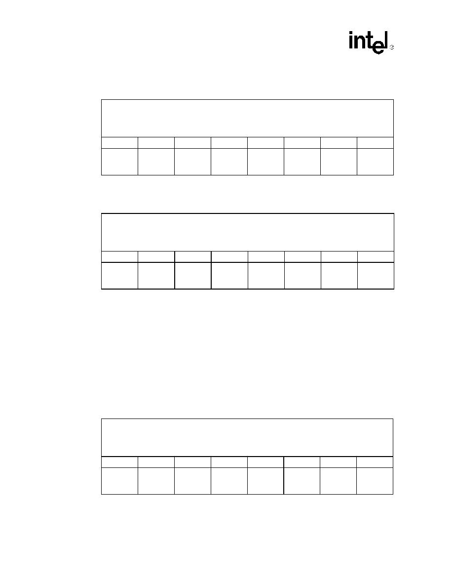
CD1400 -- UXART Serial/Parallel Controller
122
Datasheet
9.6.6
Modem Signal Value Register 1 (MSVR1
9.6.7
Modem Signal Value Register 2 (MSVR2)
The MSVR1 and MSVR2 Registers provide information regarding the state of the Modem Input
Pins (DSR*, CTS*, RI* and CD*), the current state of Printer Strobe Output Pin (PSTROBE*) and
allows control of the Modem Output Pins (DTR* and RTS*). The PSTROBE* Bit is only valid for
Channel 0; on all other channels it is not used. Writing to any of the input bits has no effect. With
the exception of the least significant two bits, the registers reflect identical data. The two are
provided as a convenience for control of the Modem Output Pins. Host software need not keep a
copy of the current state of either when controlling the other. The actual signal level on the output
is the inverse of the value placed in this register: setting the DTR Bit, for example, will cause the
DTR Output to become active-low. The state of the Modem Input Pins are also the inverse of the
value in the corresponding bit in the registers.
9.6.8
Printer Signal Value Register (PSVR)
Register Name: MSVR1
Hex Address: 6C
Register Description: Modem Signal Value Register 1
Default Value: x'00
Access: Read/Write
Bit 7
Bit 6
Bit 5
Bit 4
Bit 3
Bit 2
Bit 1
Bit 0
DSR
CTS
RI
CD
PSTROBE*
0
0
RTS
Register Name: MSVR2
Hex Address: 6D
Register Description: Modem Signal Value Register 2
Default Value: x'00
Access: Read/Write
Bit 7
Bit 6
Bit 5
Bit 4
Bit 3
Bit 2
Bit 1
Bit 0
DSR
CTS
RI
CD
PSTROBE*
0
DTR
0
Register Name: PSVR
Hex Address: 6F
Register Description: Printer Signal Value
Default Value: x'08
Access: Read/Write
Bit 7
Bit 6
Bit 5
Bit 4
Bit 3
Bit 2
Bit 1
Bit 0
PBUSY
PSLCT*
PPE*
PERROR*
PACK*
PAUTOFD*
PINIT*
PSLIN*
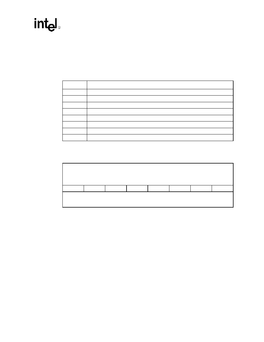
UXART Serial/Parallel Controller -- CD1400
Datasheet
123
This register groups all of the Modem Signals for Channel 0 into one register. The PSVR is only
valid for Channel 0. The most significant five bits reflect the current signal value on the Input Pins
PBUSY, PSLCT*, PPE*, PERROR* and PACK*. The values in these bits reflect the inverse of the
actual values on the input pins. A logic `0' on the input pin will be shown as a `1' in the
corresponding bits; a logic `1' on the pin will be a `0' in the register. The least significant three bits
can be used by the host software to control the Modem Output Pins PAUTOFD*, PINIT* and
PSLIN*. These bits directly control the outputs, and the values are inverted.
9.6.9
Receive Baud Rate Period Register (RBPR)
This register holds the baud rate divisor for the receiver. It is used in conjunction with the Receive
Clock Option Register (RCOR) that provides the clock that will be divided by this value. The time
period produced must equal the value for one bit time of the receive data.
When Channel Zero is programmed in the Parallel Mode, the RCOR/RBPR pair should be
programmed to produce an effective baud rate whose bit time is equal to twice the expected
PSTROBE* pulse width (see
"Registers" on page 22
for detailed parallel port programming
parameters).
Bit
Description
Bit 7
Printer Busy ≠ the current state of the Printer Busy Input (Parallel Transmit Mode).
Bit 6
Printer Select ≠ the current state of the Printer Select Input.
Bit 5
Printer Paper Empty ≠ the current state of the Printer Paper Empty Input.
Bit 4
Printer Error ≠ the current state of the Printer Error Input.
Bit 3
Printer Acknowledge ≠ the current state of the Printer Acknowledge Input.
Bit 2
Printer Autofeed ≠ the current state of the Printer Autofeed Output.
Bit 1
Printer Initialize ≠ the current state of the Printer Initialize Output.
Bit 0
Printer Selection ≠ the current state of the Printer Selection Output.
Register Name: RBPR
Hex Address: 78
Register Description: Receive Baud Rate Period
Default Value: x'41
Access: Read/Write
Bit 7
Bit 6
Bit 5
Bit 4
Bit 3
Bit 2
Bit 1
Bit 0
Binary Divisor Value
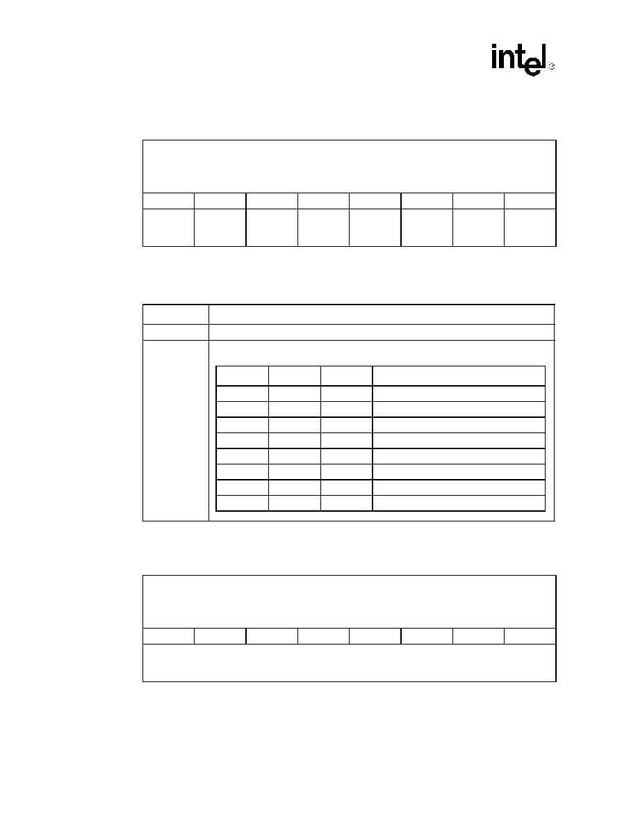
CD1400 -- UXART Serial/Parallel Controller
124
Datasheet
9.6.10
Receive Clock Option Register (RCOR)
The RCOR selects the clock source which will drive the Baud Rate Period Register (RBPR). The
value in ClkSel2-ClkSel0 selects one of five possible clocks generated from the master clock
(CLK).
9.6.11
Transmit Baud Rate Period Register (TBPR)
This register holds the baud rate divisor for the transmitter. It is used in conjunction with the
Transmit Clock Option Register (TCOR), which provides the clock that will be divided by this
value. The time period produced must equal the value for one bit time of the transmit data.
Register Name: RCOR
Hex Address: 7C
Register Description: Receive Clock Option
Default Value: x'01
Access: Read/Write
Bit 7
Bit 6
Bit 5
Bit 4
Bit 3
Bit 2
Bit 1
Bit 0
X
X
X
X
X
ClkSel2
ClkSel1
ClkSel0
Bit
Description
Bits 7:3
Not used
Bits 2:0
Register Name: TBPR
Hex Address: 72
Register Description: Transmit Baud Rate Period
Default Value: x'41
Access: Read/Write
Bit 7
Bit 6
Bit 5
Bit 4
Bit 3
Bit 2
Bit 1
Bit 0
Binary Divisor Value
ClkSel2
ClkSel1
ClkSel0
Clock Selected
0
0
0
clk0 (CLK divided by 8)
0
0
1
clk1 (CLK divided by 32)
0
1
0
clk2 (CLK divided by 128)
0
1
1
clk3 (CLK divided by 512)
1
0
0
clk4 (CLK divided by 2048)
1
0
1
Not used
1
1
0
Not used
1
1
1
Not used
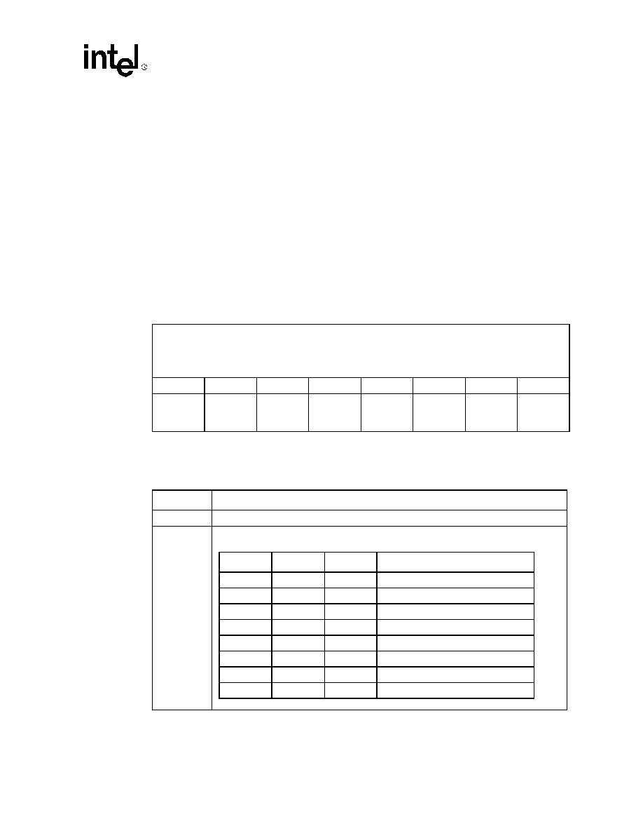
UXART Serial/Parallel Controller -- CD1400
Datasheet
125
When Channel 0 is programmed to be a parallel port, the TBPR Register determines the pulse
width of the PSTROBE* Output; the value in TCOR is not used. The least significant five (5) bits
of the register set the binary value for a counter that is decremented by the system clock (CLK
˜
2).
The range of acceptable values is 1 through 32 inclusive, which will produce pulses in the range of
100 ns to 3.2 µs for a 20-MHz clock. For example, if the TBPR is loaded with a value of 10 (hex A)
and the system clock is 20 MHz, the resulting PSTROBE* pulse width will be 1.0 µs (100 ns times
10).
Note:
During parallel operation, if the TBPR value is changed to produce a different PSTROBE* width, a
channel re-enable must be performed for the change to take affect. This is due to the manner in
which the value is used internally by the MPU. It stores a copy of the TBPR in an internal register
allowing it faster access during foreground routines when a new PSTROBE* is to be generated. A
channel re-enable is performed by writing a hex 18 (transmit) or hex 12 (receive) command to the
Channel Command Register (CCR).
9.6.12
Transmit Clock Option Register (TCOR)
The TCOR selects the clock source that will drive the Baud Rate Period Register (TBPR). The
value in ClkSel2-ClkSel0 selects one of five possible clocks generated from the master clock
(CLK).
Note:
The TCOR has no effect when Channel 0 is programmed as a parallel port.
Register Name: TCOR
Hex Address: 76
Register Description: Transmit Clock Option
Default Value: x'81
Access: Read/Write
Bit 7
Bit 6
Bit 5
Bit 4
Bit 3
Bit 2
Bit 1
Bit 0
X
X
X
X
X
ClkSel2
ClkSel1
ClkSel0
Bit
Description
Bits 7:3
Not used
Bits 2:0
ClkSel2
ClkSel1
ClkSel0
Clock Selected
0
0
0
clk0 (CLK divided by 8)
0
0
1
clk1 (CLK divided by 32)
0
1
0
clk2 (CLK divided by 128)
0
1
1
clk3 (CLK divided by 512)
1
0
0
clk4 (CLK divided by 2048)
1
0
1
Not used
1
1
0
Not used
1
1
1
Not used
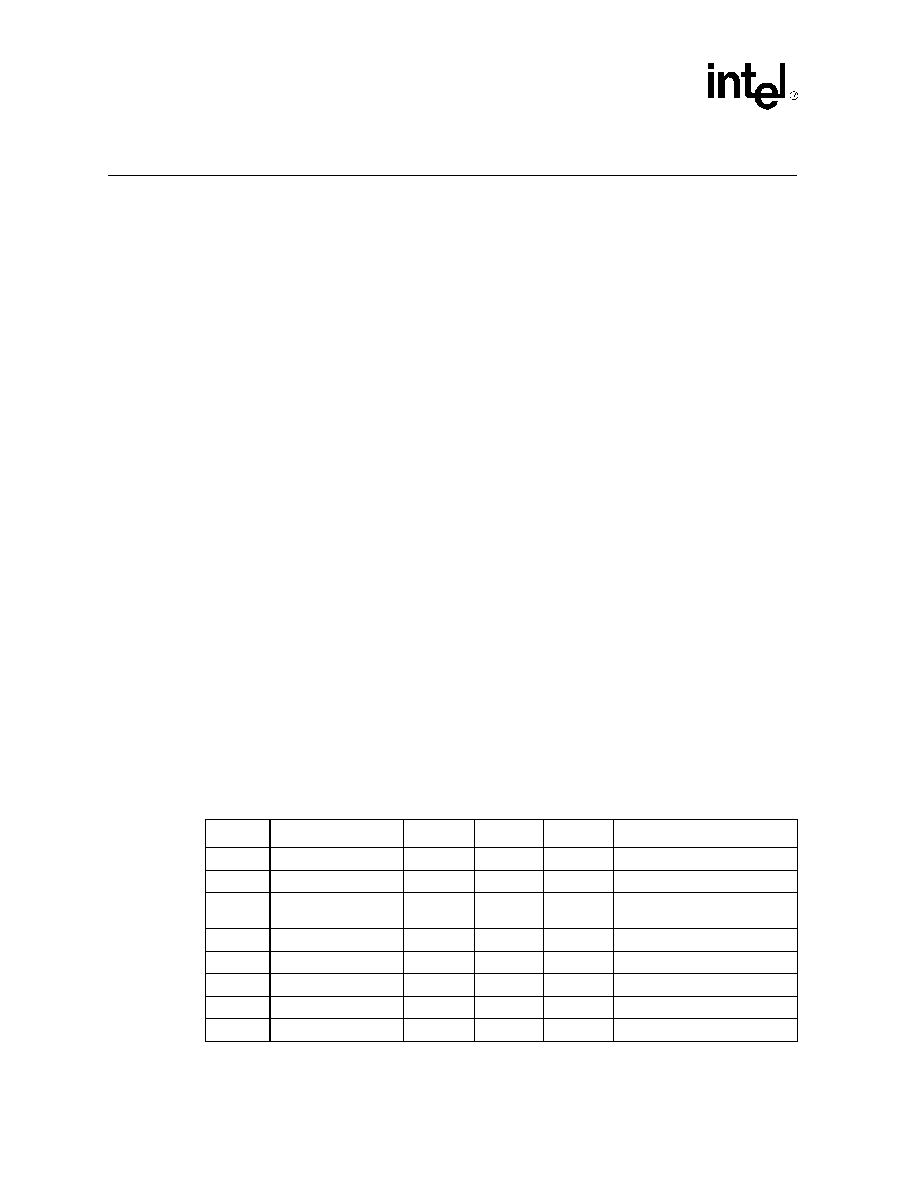
CD1400 -- UXART Serial/Parallel Controller
126
Datasheet
10.0
Electrical Specifications
Note:
Verify with your local sales office that you have the latest datasheet before finalizing a design.
10.1
Absolute Maximum Ratings
Supply voltage (V
CC
). . . . . . . . . . . . . . . . . . . . . . . . . . . . . . . . . . . . . . . . . +7.0 Volts
Input voltages, with respect to ground . . . . . . . . . . . . . . . . . . . . . . . . . . . . -0.5 Volts to V
CC
+0.5
Volts
Operating temperature (T
A
) . . . . . . . . . . . . . . . . . . . . . . . . . . . . . . . . . . . . 0
∞
C to 70
∞
C
Storage temperature . . . . . . . . . . . . . . . . . . . . . . . . . . . . . . . . . . . . . . . . . . -65
∞
C to 150
∞
C
Power dissipation . . . . . . . . . . . . . . . . . . . . . . . . . . . . . . . . . . . . . . . . . . . . 0.25 Watt
Note:
Stresses above those listed under Absolute Maximum Ratings may cause permanent damage to the
device. This is a stress rating only, and functional operation of the device at these or any conditions
above those indicated in the recommended operating conditions is not implied. Exposure to
absolute maximum rating conditions for extended periods may affect device reliability.
10.2
Recommended Operating Conditions
Supply voltage (V
CC
). . . . . . . . . . . . . . . . . . . . . . . . . . . . . . . . . . . . . . . . . 5V
±
5%
Operating free air ambient temperature . . . . . . . . . . . . . . . . . . . . . . . . . . . 0
∞
C < T
A
< 70
∞
C
System clock . . . . . . . . . . . . . . . . . . . . . . . . . . . . . . . . . . . . . . . . . . . . . . . 60 MHz
10.3
DC Electrical Characteristics
(V
CC
= 5V
±
5%, T
A
= 0
∞
C to 70
∞
C
Symbol
Parameter
Min
Max
Units
Test Conditions
V
IL
Input Low Voltage
-0.5
0.8
V
V
IH
Input High Voltage
2.0
V
CC
V
(See Note 2 on
127
)
V
OL
Output Low Voltage
0.4
V
I
OL
= 2.4 mA (see Note 1 on
127
)
V
OH
Output High Voltage
2.4
V
I
OH
= -400
µ
A
I
IL
Input Leakage Current
-10
10
µ
A
0 < V
IN
< V
CC
I
LL
Data Bus 3-State
Leakage current
-10
10
µ
A
0 < V
OUT
< V
CC
I
OC
Open-Drain Output

UXART Serial/Parallel Controller -- CD1400
Datasheet
127
Notes:
1. V
OL
for open-drain signals is 0.5V @ 16 mA sinking.
2. V
IH
is 2.7 V minimum on RESET* and CLK.
3. While the CD1400 is a highly dependable device, there are a few guidelines that will help to
ensure that the maximum possible level of overall system reliability is achieved. First, the PC
board should be designed to provide maximum isolation of noise. A four-layer board is
preferable, but a two-layer board will work if proper power and ground distribution is
implemented. In either case, decoupling capacitors mounted close to the CD1400 are strongly
recommended. Noise typically occurs when either the CD1400 data bus drivers come out of
tristate to drive the bus during a read, or when an external bus buffer turns on during a write
cycle. This noise, a rapid rate-of-change of supply current, causes ground bounce in the power
distribution traces. This ground bounce, a rise in the voltage of the ground pins, effectively
raises the input logic thresholds of all devices in the vicinity, resulting in the possibility of a 1
being interpreted as a 0.
To reduce the possibility of ground bounce affecting the operation of the CD1400, we have
specified the input-high voltage (V
IH
) of the CLOCK and RESET Pins at 2.7 volts, instead of
the TTL-standard 2.0 volts. This eliminates any sensitivity to ground bounce, even in very
noisy systems.
Although 2.7 volts is higher than the industry-standard 2.4-volt output (V
OH
) specified for
TTL, there are several simple ways to meet this specification. One choice is to use any of the
available advanced-CMOS logic families (FACT, ACL, etc.). These CMOS output buffers will
pull up close to V
CC
when not heavily loaded. In addition, AS and ALS TTL may be used if
the output of the TTL device is only driving one or two CMOS loads. As noted in the Texas
Instruments
ALS/AS Logic Data Book (1986), pages 4-18 and 4-19, the V
OH
output of these
families exceeds 3.0 volts at low-current loading. Other manufacturers publish similar data.
Intel recommends the use of one of these two options for the CLK input, to ensure fast, clean
edges. Note that the RESET Pin may, if desired, be pulled up passively with a 1K ohm (or less)
resistor.
Leakage Current
-10
10
µ
A
0 < V
OUT
< V
CC
I
CC
Power Supply Current
50
mA
CLK = 60 MHz
Input Capacitance
10
pF
C
OUT
Output Capacitance
10
pF
Symbol
Parameter
Min
Max
Units
Test Conditions
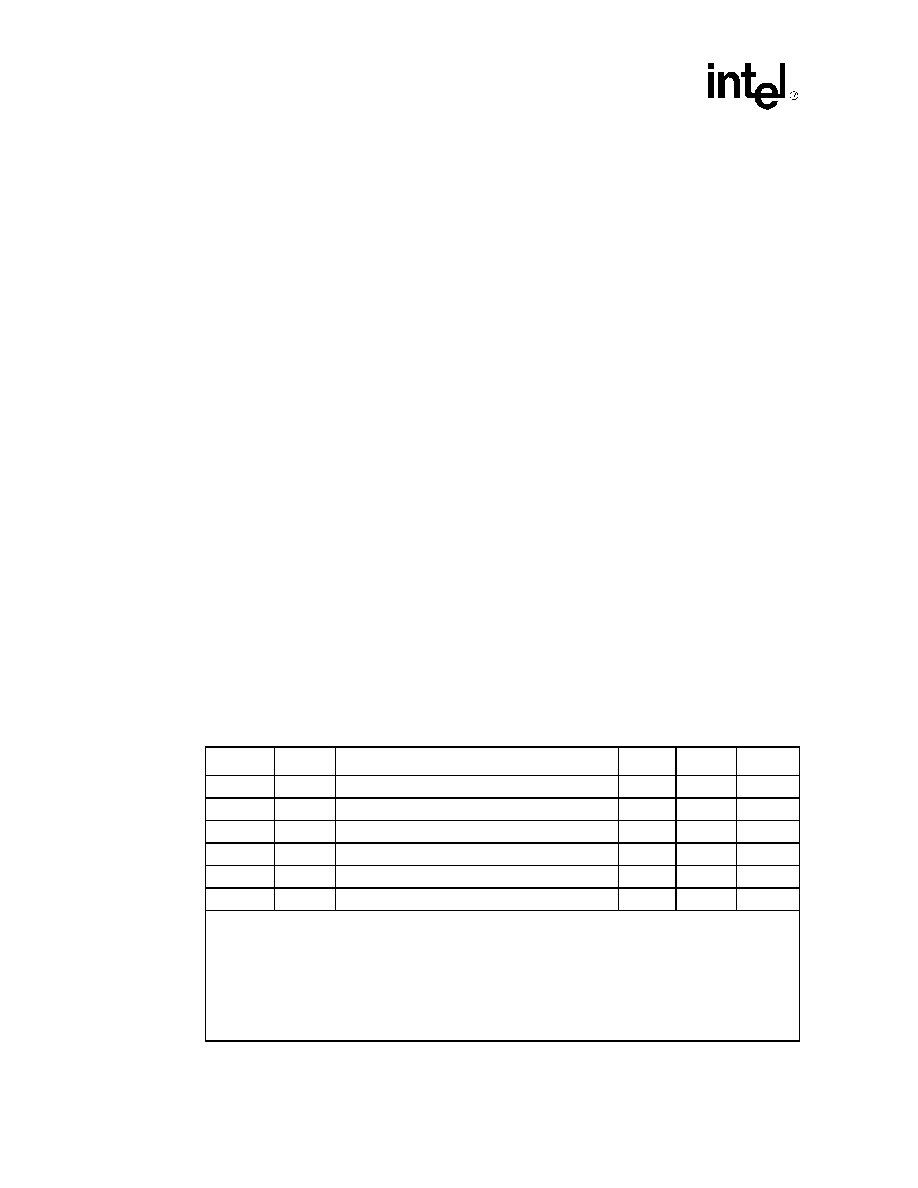
CD1400 -- UXART Serial/Parallel Controller
128
Datasheet
10.4
AC Electrical Characteristics
10.4.1
Index of Timing Information
Figure
Title
Page Number
Asynchronous Timing
. . . . . . . . . . . . . . . . . . . . . . . . . . . . . . . . . . . . . . . . . . 128
21
Reset Timing
. . . . . . . . . . . . . . . . . . . . . . . . . . . . . . . . . . 129
22
Clock Timing
. . . . . . . . . . . . . . . . . . . . . . . . . . . . . . . . . . 130
23
Asynchronous Read Cycle Timing
. . . . . . . . . . . . . . . . . . 130
24
Asynchronous Write Cycle Timing
. . . . . . . . . . . . . . . . . . 131
25
Asynchronous Service Acknowledge Cycle Timing
. . . . . 132
Synchronous Timing
. . . . . . . . . . . . . . . . . . . . . . . . . . . . . . . . . . . . . . . . . . . 132
26
Synchronous Read Cycle Timing
. . . . . . . . . . . . . . . . . . 133
27
Synchronous Write Cycle Timing
. . . . . . . . . . . . . . . . . . . 134
28
Synchronous Service Acknowledge Cycle Timing
. . . . . . 135
Parallel Port Timing
. . . . . . . . . . . . . . . . . . . . . . . . . . . . . . . . . . . . . . . . . . . . 135
29
Parallel Port Transmit Timing
. . . . . . . . . . . . . . . . . . . . . 137
30
Parallel Port Receive Timing
. . . . . . . . . . . . . . . . . . . . . . 137
10.4.2
Asynchronous Timing
Refer to the
Figure 21
through
Figure 25
on the following pages for the reference numbers in the
following table. The timing parameters shown on these pages apply to Revision H or later devices.
(V
CC
= 5V
±
5%, T
A
= 0
∞
C to 70
∞
C
Ref. #
Fig.
Parameter
MIN
MAX
Unit
t
1
21
RESET* Low pulse width
10
T
CLK
t
2
23
Address setup time to CS* or DS*
0
ns
t
3
23
R/W* setup time to CS* or DS*
0
ns
t
4
23
Address hold time after CS*
0
ns
t
5
23
R/W* hold time after CS*
0
ns
t
6
23
DTACK* low to read data valid
10
ns
NOTES:
1. Timing numbers for RESET* and CLK in the table above are valid for both asynchronous and synchronous
specifications.
2. On host I/O cycles immediately following SVCACK* cycles and writes to EOSRR, DTACK* will be delayed
by 1
µ
s. On systems that do not use DTACK* to signal the end of the I/O cycle, wait states or some other
form of delay generation must be used to assure that the CD1400 will not be accessed until after this time
period.
3. As TCLK increases, device performance decreases. A minimum clock frequency of 60 MHz is required to
guarantee performance as specified. The recommended maximum TCLK is 1000 ns.
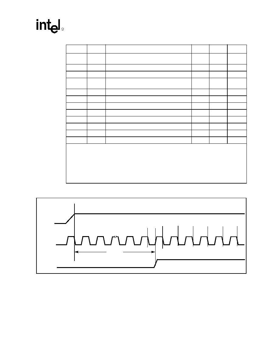
UXART Serial/Parallel Controller -- CD1400
Datasheet
129
Note:
For synchronous systems, it is necessary to know the clock cycle number so that interface circuitry
can stay in lock-step with the device. CLK numbers can be determined if RESET* is released
within the range t
a
- t
b
; t
a
is defined as 10 ns minimum after the falling edge of the clock; t
b
is
defined as 5 ns minimum before the next falling edge of the clock. If these conditions are met, the
cycle starting after the second falling edge will be known to be C1. See the synchronous timing
diagrams for additional information. Asynchronous systems need not be concerned with clock
numbers.
t
7
23
DTACK* low from CS* or DS
2
3 T
CLK
5T
CLK
+4
0
ns
t
8
23
Data Bus tristate after CS* or DS* high
0
25
ns
t
9
23
CS* or DGRANT* high from DTACK* low
0
ns
t
10
23
DTACK* inactive from CS* or DGRANT* and DS*
high
30
ns
t
11
23
DS* high pulse width
10
ns
t
12
24
Write data valid from CS* and DS* low
2T
CLK
ns
t
13
24
Write data hold time after DS* high
0
ns
t
14
22
Clock period (TCLK)
1, 3
30
200
ns
t
15
22
Clock low time
1
0.4T
CLK
0.6T
CLK
ns
t
16
22
Clock high time
1
0.4T
CLK
0.6T
CLK
ns
t
17
25
Propagation delay, DGRANT* and DS* to DPASS*
30
ns
t
18
25
Setup time, SVCACK* to DS* and DGRANT*
10
ns
Figure 21. Reset Timing
Ref. #
Fig.
Parameter
MIN
MAX
Unit
NOTES:
1. Timing numbers for RESET* and CLK in the table above are valid for both asynchronous and synchronous
specifications.
2. On host I/O cycles immediately following SVCACK* cycles and writes to EOSRR, DTACK* will be delayed
by 1
µ
s. On systems that do not use DTACK* to signal the end of the I/O cycle, wait states or some other
form of delay generation must be used to assure that the CD1400 will not be accessed until after this time
period.
3. As TCLK increases, device performance decreases. A minimum clock frequency of 60 MHz is required to
guarantee performance as specified. The recommended maximum TCLK is 1000 ns.
t
1
VCC
CLK
RESET*
t
a
t
b
C1
C2
C1
C2
C1
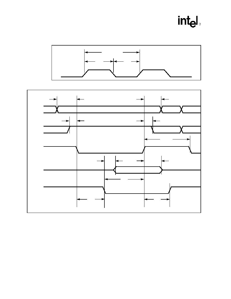
CD1400 -- UXART Serial/Parallel Controller
130
Datasheet
Figure 22. Clock Timing
Figure 23. Asynchronous Read Cycle Timing
t
14
t
16
t
15
A[0:6]
R/W*
CS*
DTACK*
DB[0:7]
t
11
t
2
t
4
t
3
t
6
t
7
t
10
t
9
t
8
t
5
DS*
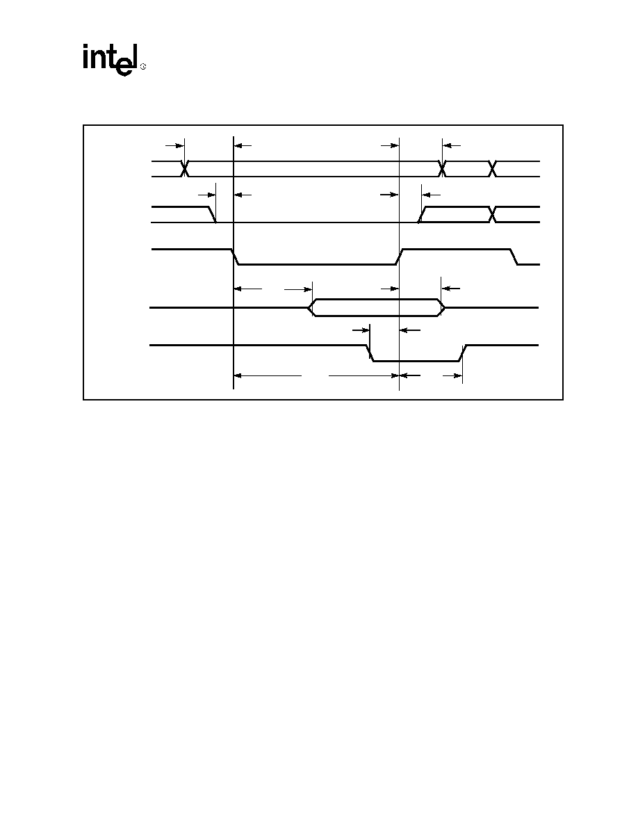
UXART Serial/Parallel Controller -- CD1400
Datasheet
131
Figure 24. Asynchronous Write Cycle Timing
A[0:6]
R/W*
DTACK*
DB[0:7]
t
2
t
4
t
3
t
12
t
7
t
10
t
9
t
13
t
5
CS*
DS*
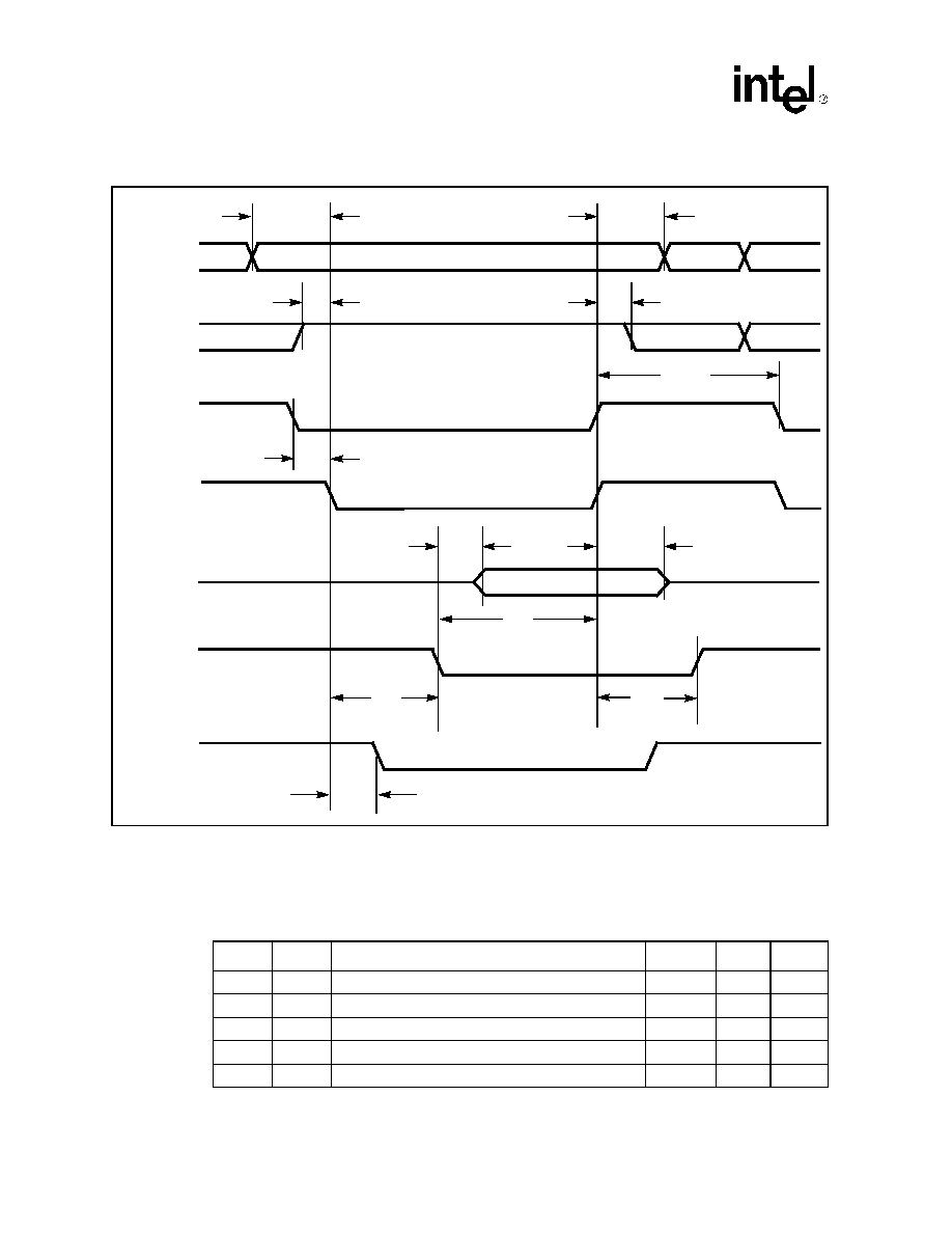
CD1400 -- UXART Serial/Parallel Controller
132
Datasheet
10.4.3
Synchronous Timing
Refer to
Figure 26
through
Figure 28
on the following pages for the reference numbers in the table
below.
Figure 25. Asynchronous Service Acknowledge Cycle Timing
A[0:6]
R/W*
SVCACK*
DGRANT*
DTACK*
DB[0:7]
t
11
t
2
t
4
t
3
t
6
t
7
t
10
t
9
t
8
t
5
t
17
DPASS*
DS*
t
18
Ref. #
Fig.
Parameter
MIN
MAX
Unit
t
1
26
Setup time, CS* and DS* to C1 falling edge
5
ns
t
2
26
Setup time, R/W* to C1 falling edge
0
ns
t
3
26
Setup time, address valid to C1 falling edge
0
ns
t
4
26
C3 falling edge to data valid
40
ns
t
5
26
DTACK* low from C4 falling edge
30
ns
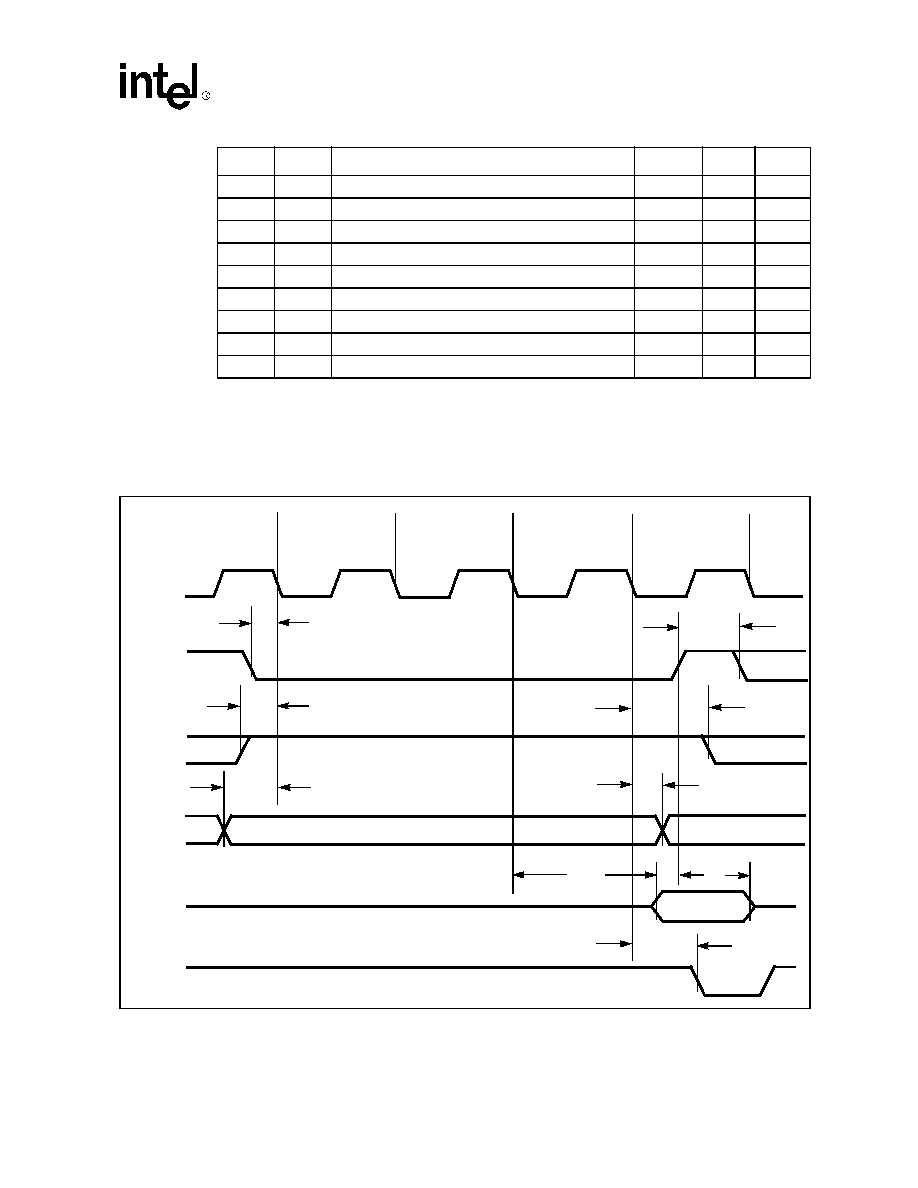
UXART Serial/Parallel Controller -- CD1400
Datasheet
133
Note:
On host I/O cycles immediately following SVCACK* cycles and writes to EOSRR, DTACK* will
be delayed by 1
µ
s. On systems that do not use DTACK* to signal the end of the I/O cycle, wait
states or some other form of delay generation must be used to assure that the CD1400 will not be
accessed until after this time period.
t
6
26
CS* and DS* trailing edge to data bus high-impedance
25
t
7
26
CS* and DS* inactive between host accesses
10
ns
t
8
26
Hold time, R/W* after C4 falling edge
20
ns
t
9
26
Hold time, address valid after C4 falling edge
0
ns
t
10
27
Setup time, write data valid to C3 falling edge
0
ns
t
11
28
Setup time, DS* and DGRANT* to C1 falling edge
20
ns
t
12
28
Setup time, SVCACK* to DS* and DGRANT*
10
ns
t
13
28
Hold time, write data valid after C4 falling edge
0
ns
t
14
28
Propagation delay, DS* and DGRANT* to DPASS*
30
ns
Figure 26. Synchronous Read Cycle Timing
Ref. #
Fig.
Parameter
MIN
MAX
Unit
t
1
t
2
t
3
t
4
t
8
t
9
t
6
C1
C2
C3
C4
CLK
DS*, CS*
R/W*
A[6:0]
DB[7:0]
DTACK*
t
5
t
7
CD1400 -- UXART Serial/Parallel Controller
134
Datasheet
Figure 27. Synchronous Write Cycle Timing
t
1
t
2
t
3
t
8
t
9
t
13
C1
C2
C3
C4
CLK
DS*, CS*
R/W*
A[6:0]
DB[7:0]
DTACK*
t
5
t
10
t
7
UXART Serial/Parallel Controller -- CD1400
Datasheet
135
10.4.4
Parallel Port Timing Specifications
Refer to
Figure 29
and
Figure 30
for identification of reference numbers in the following table.
Note that the functions of PACK* and PSTROBE* are opposite depending on the direction of data
movement, however the directions of PSTROBE* and PACK* do not change. The PACK* Signal
on the CD1400 is always an input, and the PSTROBE* is always an output. The apparent function
is changed by the external signals they are connected to and the direction of data movement. The
tables below use the CD1400 pin names for the signals.
The following table shows the timing specifications for the parallel port when it is programmed in
Transmit Mode (Receive Mode is on the following page). The PSTROBE* Output provides the
data strobe function and the PACK* Input is connected to the acknowledge signal from the
receiving device.
Transmit Timing (see
Figure 29
).
Figure 28. Synchronous Service Acknowledge Cycle Timing
t
12
t
2
t
4
t
8
t
6
C1
C2
C3
C4
CLK
DS*
R/W*
DB[7:0]
DTACK*
t
5
t
7
SVCACK*
DGRANT*
t
11
t
14
DPASS*
CD1400 -- UXART Serial/Parallel Controller
136
Datasheet
The following table shows the timing specifications for the parallel port when it is programmed in
the Receive Mode. The transmitting device connects its strobe output to the CD1400 PACK* Input
and its acknowledge input to the CD1400 PSTROBE* Output.
Receive Timing (see
Figure 30
).
Notes:
1. The width of the PSTROBE* pulse is set by the programmed value in the TBPR Register and
will be equal to the system clock (CLK) divided by two, multiplied by the binary value
continued in the least significant five (5) bits. The range of values is 1 to 32 (1 to 1F hex).
2. For highest performance, the RCOR/RBPR Register pair should be programmed for a baud
rate whose half-bit time is slightly greater than the expected length of the STROBE pulse
width (see
"Functional Description" on page 29
for detailed parallel port programming
information.
3. This parameter is guaranteed by design but cannot be measured by ATE.
Ref. #
Fig.
Parameter
MIN
MAX
Unit
t
P
1
29
Setup time, PD[7:0] to PSTROBE* falling
edge
2T
CLK
*2
t
P
2
29
PACK* rising edge to PSTROBE* falling
edge
5
2T
CLK
*350
t
P
3
29
PSTROBE* pulse width
1
2T
CLK
2T
CLK
*32
t
P
4
29
PACK* pulse width
2
250
ns
t
p
5
29
PSTROBE* to PACK* time-out
5
2T
CLK
*10
Ref. #
Fig.
Parameter
MIN
MAX
Unit
t
P
6
30
Setup time, PD[7:0] to PACK* rising edge
15
ns
t
P
7
30
Hold time, PD[7:0] after PACK* rising edge
20
ns
t
P
8
30
PSTROBE* pulse width
1
(ACK function)
2T
CLK
2T
CLK
*32
t
P
9
30
PACK* to PSTROBE* time-out
3
2T
CLK
*15
t
P
10
30
PACK* pulse width
2
(STROBE function)
250
ns
t
P
11
30
PACK* falling edge to PBUSY rising edge
30
ns
t
P
12
30
PSTROBE* falling edge to PACK* falling
edge
3
2T
CLK
*10
t
P
13
30
PSTROBE* rising edge to PBUSY falling
edge
30
ns
UXART Serial/Parallel Controller -- CD1400
Datasheet
137
Note:
PBUSY is optional when the parallel port is operating in the Transmit Mode. The CD1400 will not
activate PSTROBE* to begin the next data transaction until the receiver has acknowledged the
previous transaction via the PACK* Signal; PBUSY is not used as a flow control signal in Transmit
Mode.
Figure 29. Parallel Port Transmit Timing
Figure 30. Parallel Port Receive Timing
PSTROBE*
PD[7:0]
PACK*
t
P
1
t
P
2
t
P
4
t
P
3
PBUSY
OPTIONAL
t
P
5
PACK* Pin
PD[7:0]
PSTROBE* Pin
t
P
6
t
P
7
t
P
8
t
P
9
t
P
10
(STROBE function)
(ACK function)
PBUSY
t
P
12
t
P
13
t
P
11
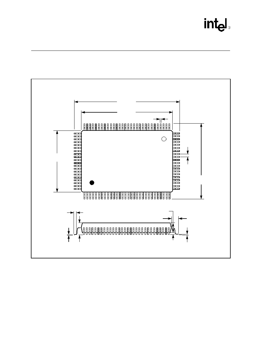
CD1400 -- UXART Serial/Parallel Controller
138
Datasheet
11.0
Package Specifications
11.1
100-Pin MQFP (JEDEC) Package
Notes:
1. Dimensions are in millimeters (inches), and controlling dimension is millimeter.
2. Before beginning any new design with this device, please contact Intel for the latest package
information.
Pin 1 Indicator
Pin 1
19.90 (0.783)
22.95 (0.904)
23.45 (0.923)
20.10 (0.791)
16.95 (0.667)
17.45 (0.687)
13.90 (0.547)
14.10 (0.555)
0.13 (0.005)
0.23 (0.009)
1.60 (0.063) REF
2.57 (0.101)
2.87 (0.113)
0.65 (0.026)
0.95 (0.037)
0∞ MIN
7∞ MAX
0.22 (0.009)
0.38 (0.015)
0.65
(0.0256)
BSC
Pin 100
3.40
0.25
(0.134)
MAX
(0.010)
MIN
CD1400-10QC-J
100-Pin MQFP
UXART Serial/Parallel Controller -- CD1400
Datasheet
139
12.0
Ordering Information
Contact Intel for up-to-date information on revisions.
SCD140010QCJ
Product Line:
Part Number
Internal Reference Number
Package Type: MQFP
Metric quad flat pack
Temperature Range
C = Commercial
Revision
Communications, Data
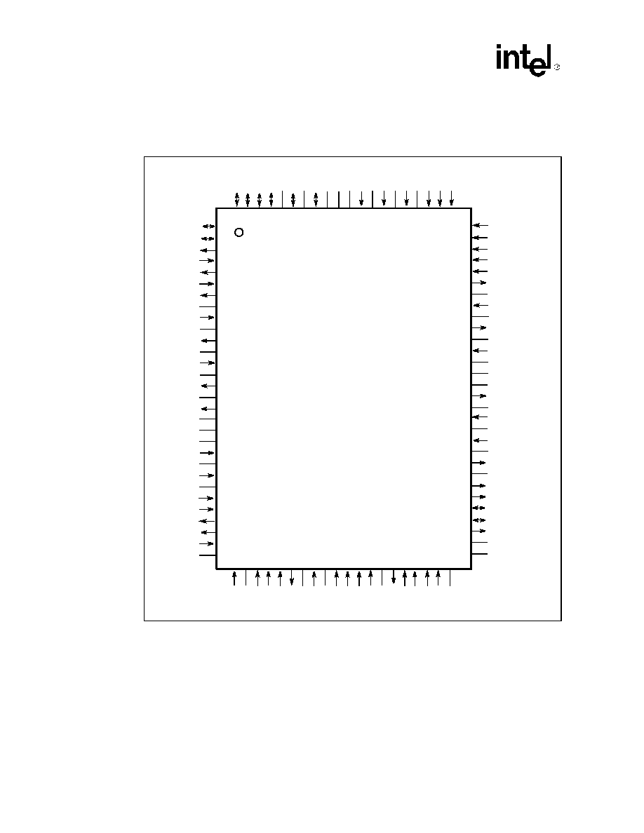
CD1400 -- UXART Serial/Parallel Controller
140
Datasheet
12.1
Pin Diagram -- 100-Pin MQFP
Note:
N/C means no connection (make no connections to these pins).
Figure 31. Pin Diagram -- 100-Pin MQFP
84
85
86
87
88
89
90
91
92
93
94
95
96
97
98
99
10
0
1
2
3
4
5
6
7
8
9
10
11
12
13
14
15
16
17
83
82
81
CD1400
100-Pin MQFP
GND
A[
2
]
N/C
A[
1
]
N/C
A[
0
]
N/
C
GND
N/C
DB[7
]
VCC
DB[6
]
GN
D
DB[5
]
DB[4
]
DB[2
]
DB[1]
DB[0]
TXD0
RXD0
TXD1
RXD1
TXD2
VCC
RXD2
N/C
TXD3
GND
RXD3
N/C
DTR3*
GND
RTS3*
A[6]
RESET*
CS*
DS*
R/W*
DTACK*
N/C
CLK
GND
N/C
DPASS*
DGRANT*
N/C
GND
VCC
N/C
SVCREQM*
18
19
20
21
22
23
24
25
26
27
28
29
30
80
79
78
77
76
75
74
73
72
71
70
69
68
67
66
65
64
63
62
61
60
59
58
57
56
55
54
53
52
51
47
46
45
44
43
42
41
40
39
38
37
36
35
34
33
32
31
48
49
50
DB[3
]
A[
3
]
A[
4
]
A[
5
]
N/C
VCC
N/C
CTS3*
N/C
DSR3*
GND
RI3*
DTR2*
CD3*
RTS2*
CTS2*
VCC
SVCREQT*
N/C
SVCREQR*
GND
SVCACKM*
VCC
SVCACKT*
SVCACKR*
PD[0]
PD[1]
PAUTOFD*
N/C
GND
DSR0
*
CT
S0
*
RT
S0
*
GND
DT
R0
*
CD1
*
RI1
*
DSR1
*
VCC
CT
S1
*
GND
RT
S1
*
DT
R1
*
CD
2
*
RI2
*
DSR2
*
GND
RI0
*
CD0
*
VCC
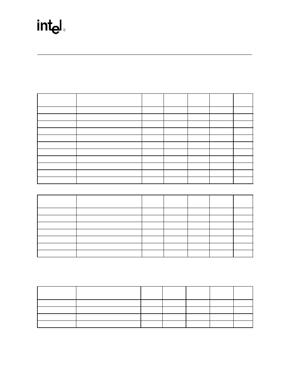
UXART Serial/Parallel Controller -- CD1400
Datasheet
141
13.0
Quick Reference
13.1
CD1400 Register Map
Note:
The page numbers shown in these tables indicate the page where the detailed description of the
register may be found.
Table 20. Global Registers
Symbol
Register Name
Access
A[6:0]
Default
Value
Hex
Address
Page
GFRCR
Global Firmware Revision Code
R/W
100 0000
x'48
40
88
CAR
Channel Access
R/W
110 1000
x'C0
68
88
GCR
Global Configuration
R/W
100 1011
x'00
4B
89
SVRR
Service Request
R
110 0111
x'00
67
104
RICR
Receive Interrupting Channel
R/W
100 0100
x'00
44
90
TICR
Transmit Interrupting Channel
R/W
100 0101
x'00
45
90
MICR
Modem Interrupting Channel
R/W
100 0110
x'00
46
91
RIR
Receive Interrupt
R/W
110 1011
x'18
6B
92
TIR
Transmit Interrupt
R/W
110 1010
x'10
6A
92
MIR
Modem Interrupt
R/W
110 1001
x'08
69
92
PPR
Prescaler Period
R/W
111 1110
x'FF
7E
93
Table 21. Virtual Registers
Symbol
Register Name
Access
A[6:0]
Default
Value
Hex
Address
Page
RIVR
Receive Interrupt Vector
R
100 0011
x'00
43
94
TIVR
Transmit Interrupt Vector
R
100 0010
x'00
42
94
MIVR
Modem Interrupt Vector
R
100 0001
x'00
41
95
TDR
Transmit Data
W
110 0011
x'00
63
96
RDSR
Receive Data/Status
R
110 0010
x'00
62
96
MISR
Modem Interrupt Status
R
100 1100
x'00
4C
98
EOSRR
End Of Service Request
W
110 0000
x'00
60
98
Table 22. Channel Registers (Sheet 1 of 2)
Symbol
Register Name
Access
A[6:0]
Default
Value
Hex
Address
Page
LIVR
Local Interrupt Vector
R/W
0011000
x'00
18
99
CCR
Channel Command
R/W
0000101
x'00
05
99
SRER
Service Request Enable
R/W
0000110
x'00
06
104
COR1
Channel Option 1
R/W
0001000
x'00
08
105
CD1400 -- UXART Serial/Parallel Controller
142
Datasheet
COR2
Channel Option 2
R/W
0001001
x'00
09
107
COR3
Channel Option 3
R/W
0001010
x'00
0A
108
COR4
Channel Option 4
R/W
0011110
x'00
1E
110
COR5
Channel Option 5
R/W
0011111
x'00
1F
111
CCSR
Channel Control Status
R
0001011
x'00
0B
112
RDCR
Received Data Count
R
0001110
x'00
0E
114
SCHR1
Special Character 1
R/W
0011010
x'00
1A
116
SCHR2
Special Character 2
R/W
0011011
x'00
1B
116
SCHR3
Special Character 3
R/W
0011100
x'00
1C
116
SCHR4
Special Character 4
R/W
0011101
x'00
1D
117
SCRL
Special Character Range, Low
R/W
0100010
x'00
22
117
SCRH
Special Character Range, High
R/W
0100011
x'00
23
117
LNC
LNext Character
R/W
0100100
x'00
24
118
MCOR1
Modem Change Option 1
R/W
0010101
x'00
15
118
MCOR2
Modem Change Option 2
R/W
0010110
x'00
16
120
RTPR
Receive Time-out Period
R/W
0100001
x'00
21
121
MSVR1
Modem Signal Value 1
R/W
1101100
x'00
6C
122
MSVR2
Modem Signal Value 2
R/W
1101101
x'00
6D
122
PSVR
Printer Signal Value
R/W
1101111
x'08
6F
122
RBPR
Receive Baud Rate Period
R/W
1111000
x'41
78
123
RCOR
Receive Clock Option
R/W
1111100
x'01
7C
124
TBPR
Transmit Baud Rate Period
R/W
1110010
x'41
72
124
TCOR
Transmit Clock Option
R/W
1110110
x'81
76
125
Table 23. Bit Definitions (Sheet 1 of 3)
Name
Bit 7
Bit 6
Bit 5
Bit 4
Bit 3
Bit 2
Bit 1
Bit 0
Global Registers
GFRCR
Firmware Revision Code
CAR
poll
poll
poll
poll
poll
0
C1
C0
GCR
P/S*
0
0
0
0
0
0
0
SVRR
0
0
0
0
0
SRM
SRT
SRR
RICR
X
X
X
X
C1
C0
X
X
TICR
X
X
X
X
C1
C0
X
X
MICR
X
X
X
X
C1
C0
X
X
RIR
rxireq
rbusy
runfair
1
1
0
ch[1]
ch[0]
TIR
txireq
tbusy
tunfair
1
0
0
ch[1]
ch[0]
Table 22. Channel Registers (Sheet 2 of 2)
Symbol
Register Name
Access
A[6:0]
Default
Value
Hex
Address
Page
UXART Serial/Parallel Controller -- CD1400
Datasheet
143
MIR
mdireq
mbusy
munfair
0
1
0
ch[1]
ch[0]
PPR
Binary Value
Virtual Registers
RIVR
X
X
X
X
X
IT2
IT1
IT0
TIVR
X
X
X
X
X
IT2
IT1
IT0
MIVR
X
X
X
X
X
IT2
IT1
IT0
TDR
Transmit Character
RDSR(Data)
Received Character
RDSR(Status)
Time-out
SC Det2
SC Det1
SC Det0
Break
PE
FE
OE
MISR
DSRch
CTSch
RIch
CDch
0
0
0
0
EOSRR
X
X
X
X
X
X
X
X
Channel Registers
LIVR
X
X
X
X
X
IT2
IT1
IT0
CCR
Res Chan
COR Chg
Send SC
Chan Ctl
D3
D2
D1
D0
CCR(Format1)
Res Chan
0
0
0
0
0
FTF
Type
CCR(Format2)
0
COR Chg
0
0
COR3
COR2
COR1
0
CCR(Format3)
0
0
Send SC
0
0
SSPC2
SSPC1
SSPC0
CCR(Format4)
0
0
0
Chan Ctl
XMT EN
XMT DIS
RCV EN
RCV DIS
SRER
MdmCh
0
0
RxData
0
TxRdy
TxMpty
NNDT
COR1
Parity
ParM1
ParM0
Ignore
Stop1
Stop0
ChL1
ChL0
COR2
IXM
TxIBE
ETC
LLM
RLM
RtsAO
CtsAE
DsrAE
COR3(Serial)
SCDRNG
SCD34
FCT
SCD12
RxTh3
RxTh2
RxTh1
RxTh0
COR3(Parallel)
0
0
0
RxTh4
RxTh3
RxTh2
RxTh1
RxTh0
COR4
IGNCR
ICRNL
INLCR
IGNBRK
-BRKINT
PEH[2]
PEH[1]
PEH[0]
COR5
ISTRIP
LNE
CMOE
0
0
EBD
ONLCR
OCRNL
CCSR(Serial)
RxEn
RxFloff
RxFlon
0
TxEn
TxFloff
TxFlon
0
CCSR(Parallel)
RxEn
0
0
0
TxEn
0
0
0
RDCR(Serial)
0
0
0
0
CT3
CT2
CT1
CT0
RDCR(Parallel)
0
0
0
CT4
CT3
CT2
CT1
CT0
SCHR1
Special Character 1
SCHR2
Special Character 2
SCHR3
Special Character 3
SCHR4
Special Character 4
SCRL
Character Range Low
SCRH
Character Range High
LNC
LNext Character
MCOR1(Serial)
DSRzd
CTSzd
RIzd
CDzd
DTRth3
DTRth2
DTRth1
DTRth0
Table 23. Bit Definitions (Sheet 2 of 3)
Name
Bit 7
Bit 6
Bit 5
Bit 4
Bit 3
Bit 2
Bit 1
Bit 0
CD1400 -- UXART Serial/Parallel Controller
144
Datasheet
Note:
Bit 3 of MSVR1 and MSVR2 show the state of the PSTROBE* output only on Channel 0.
MCOR1(Parallel
)
PBUSYzd
PSLCTzd
PPEzd
PERRORz
d
0
0
0
0
MCOR2(Serial)
DSRod
CTSod
RIod
CDod
0
0
0
0
MCOR2(Parallel
)
PBUSYod
PSLCTod
PPEod
PERRORo
d
0
0
0
0
RTPR
Binary Count Value
MSVR1
DSR
CTS
RI
CD
PSTROBE*
0
0
RTS
MSVR2
DSR
CTS
RI
CD
PSTROBE*
0
DTR
0
PSVR
PBUSY
PSLCT*
PPE*
PERROR*
PACK*
PAUTOFD*
PINIT*
PSLIN*
RBPR
Binary Divisor Value
RCOR
X
X
X
X
X
ClkSel2
ClkSel1
ClkSel0
TBPR
Binary Divisor Value
TCOR
X
X
X
X
X
ClkSel2
ClkSel1
ClkSel0
Table 23. Bit Definitions (Sheet 3 of 3)
Name
Bit 7
Bit 6
Bit 5
Bit 4
Bit 3
Bit 2
Bit 1
Bit 0