High Performance Scalable DSP Chip
FEATURES/BENEFITS:
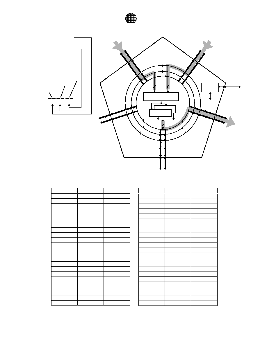
DESCRIPTION:
The DSP24 breaks the computational bottlenecks
associated with real time DSP, with the additional benefit
of radically reduced software overhead. Most
demanding DSP tasks such as frequency domain digital
filtering are reduced to less than a dozen DSP24
machine instructions.
The DSP24 concentrates on performing DSP algorithms
using the efficiencies of the FFT. Applications using time
domain techniques such as the DFT and FIR increase in
operations by a N squared function. These same
applications using FFT techniques increase in
operations by N x Log (N), a radical reduction.
2
Multiple chips can be cascaded for higher radices, two
cascaded chips will perform a 1024 radix, this gives a 1
million point transform in two passes at a startling 50
MHz complex continuous sample rate.
The DSP24 was designed using DSP Architectures Inc
macro cells and super cells. The end customer can use
the DSP24 as a silicon core and surround the chip with
proprietary circuitry to further enhance the application
and reduce his overall application hardware.
DSP24
Data Sheet
10/1/02
48
48
48
48
48
48
48
48
48
Memory A
Memory B
Scalable DSP Logic
Scheduler/
Controller
System
Controls
&Test
PROM
Interface
PORT E
PORT C
PORT B
PORT A
80/100 MHz operation on an unlimited array size, with
support for 2-D and 3-D signal/image processing.
100 MHz execution speed allows a complex sample rate
of 50 MHz for a 1K complex FFT, with a window included
Two DSP24's cascaded without external memory perform
a Radix 1024 at a 100 MHz complex sample rate
Supports DSP, Complex math, Matrix math, FIRs, Block
Adds, Subtracts, Complex magnitude, etc.
Highly scalable architecture allows DSP24 chips or die
to be cascaded for higher radices and extended functions
24 bit complex FFT's with no overhead block floating point
gives signal/noise greater than floating point
Five complex bi-directional data ports for highly flexible
(any port to any port) data routing
Radix 2, Radix 4, Radix 8, Radix 16, and Radix 32
instructions, perform 1K complex FFT in two passes
On chip ROM for transform coefficients and window
functions, window free on all radices
Macro functions buried in the chip architecture dramatically
reduces software development, on chip program controller
Advanced sub-micron, very low power 3.3 volt operation.
High Performance BGA Package
Enhanced real only FFT support, FFTNN and FFT2N, plus
stacked FFTs to reduce latency
High Reliability, High Temp, Rad Hard versions available
ASIC silicon cores, Macro cells, Super cells, MCMs, and
custom constructs available
PORT D
Control
24
24
24
24
24
24
24
24
24
24
24
24
24
24
24
24
24
24
24
X
Y
Real
Real
Real
24 Real
Real
Imag
Imag
Imag
Imag
Imag
DSP24
S
U
B
T
U
P
T
U
O
S
U
B
T
U
P
T
U
O
S
U
B
T
U
P
N
I
Y
S
U
B
T
U
P
N
I
Y
S
U
B
T
U
P
N
I
X
S
U
B
T
U
P
N
I
X
100 MHz, 24-BIT PERFORMANCE:
1024 point complex FFT........................
Complex FIR Filter ...............................
Complex 16 x 16 Matrix Multiply ..........
Real FIR Filter ......................................
Complex Multiply .................................
32K point complex FFT.........................
approx. 22
m
sec
approx. 990
m
sec
41
m
sec
5 nsec/tap
10 nsec
10 nsec/tap
Architectures
DSP
DSP
Architectures
Architectures
TM
Transform Your World
TM
Transform Your World
DSP
DSP
Data Sheet
Page 2
DSP24
Digital Signal Processor
Figure 1. FFT Based Approach
PASS 1
BFLY4
PASS 2
BFLY4
PASS 3
BFLY4
PASS 4
BWND4
PASS 6
BFLY4
PASS 5
BFLY4
1
0
2
3
4
5
6
7
8
9
10
11
12
13
14
15
16
17
18
19
20
21
22
23
24
25
26
27
28
29
30
31
32
33
34
35
36
37
38
39
40
41
42
43
44
45
46
47
48
49
50
51
52
53
54
55
56
57
58
59
60
61
62
63
16
0
32
48
4
20
36
52
8
24
40
56
12
28
44
60
1
17
33
49
5
21
27
53
9
25
41
57
13
29
45
61
2
18
34
50
6
22
38
54
10
26
42
58
14
30
46
62
3
19
35
51
7
23
39
55
11
27
43
59
15
31
47
63
1
0
2
3
4
5
6
7
8
9
10
11
12
13
14
15
16
17
18
19
20
21
22
23
24
25
26
27
28
29
30
31
32
33
34
35
36
37
38
39
40
41
42
43
44
45
46
47
48
49
50
51
52
53
54
55
56
57
58
59
60
61
62
63
16
0
32
48
4
20
36
52
8
24
40
56
12
28
44
60
1
17
33
49
5
21
27
53
9
25
41
57
13
29
45
61
2
18
34
50
6
22
38
54
10
26
42
58
14
30
46
62
3
19
35
51
7
23
39
55
11
27
43
59
15
31
47
63
FFT
FFT
-1
first pass on inverse FFT
includes the filter response multiply
first pass on FFT includes the
window multiply, if any.
B
U
F
F
E
R
B
U
F
F
E
R
PASS 1
PASS 2
PASS 3
PASS 4
PASS 5
PASS 6
100 MSPS
100 MSPS
FFT
Filter Response
Coefficients
Multiply
FFT
Input
Output
-1
MMU-24
HIGH PERFORMANCE
CONFIGURATION
MMU-24
MMU-24
DSP24
S
R
A
M
SRAM
S
R
A
M
B
U
F
F
E
R
B
U
F
F
E
R
Ar
Dr
Er
Di
Ei
Br
Bi
Ai
Cr
Ci
PASS 1
FUNCTION
CODE
DATA
FLOW
SYSTEM CTL
PROM
PASS 2
PASS 3
PASS 4
PASS 5
PASS 6
6
9
Filter Response Coefficients
Control
Control
Control
Control
Input
Output
24
24
24
24
24
24
24
24
24
24
DSP
Architectures
Digital Signal Processor
Data Sheet
Page 3
DSP24
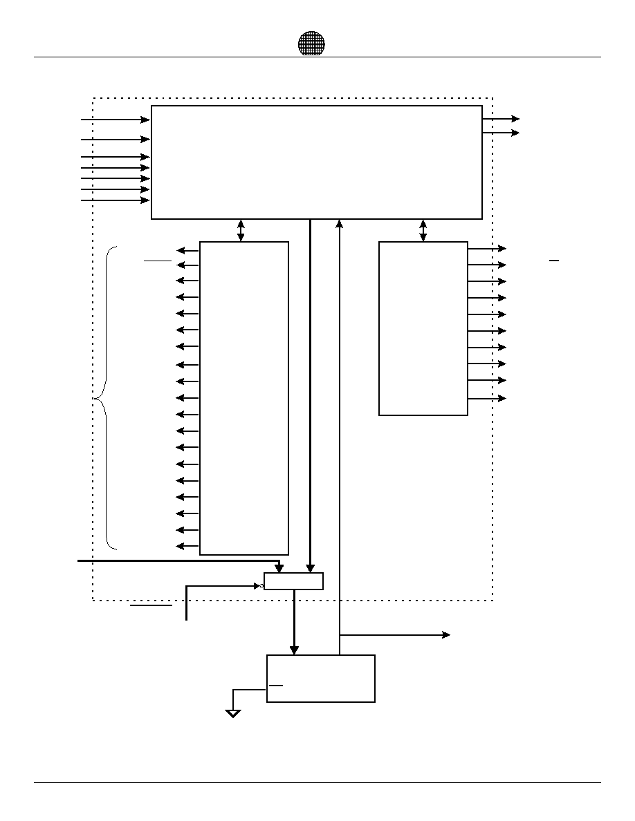
Figure 2. DSP24 Block Diagram
DSP
Architectures
MMU R/W
MMU A0
MMU START
MMU CS[4:0]
MMU TCA
MMU TCB
MMU TCC
MMU TCD
MMU TCE
SYSCLK
SYSCLKEN
AR [23:0]
AI [23:0]
BR [23:0]
BI [23:0]
CR [23:0]
CI [23:0]
DR [23:0]
DI [23:0]
ER [23:0]
EI [23:0]
CLKEIN
CLKDIN
CLKCIN
CLKBIN
CLKAIN
EOE
DOE
COE
BOE
AOE
PI1
PI0
DZO
XZI
YZI
XCI
YCI
DOCI
DOCR
XCR
YCR
YSFI[3:0]
XSFI[3:0]
XSFISEL
XSWAP
YSWAP
BFPI[5:0]
BFPO[5:0]
DSFO[3:0]
JDO
JRST
JDI
JMS
JCK
BUSY
RESET
SYNCIN[1:0]
SYNCOUT[1:0]
START/STOP
GO[1:0]
SCHSEL
ADDR[15:0]
ADDREN
SCH DB[7:0]
ALG[7:0]
POUT[2:0]
DF[8:0]
ENA
ENB
FC[5:0]
SYSTEM
AND
PORT
CLOCKS
MMU-24
CONTROL
BI-DIRECTIONAL
DATA PORTS
BLOCK FLOATING
POINT CONTROL
DATA CONDITIONING
SWITCHES
TEST/JTAG
SYSTEM
SYNCHRONIZATION
PROM
INTERFACE
DATA FLOW
&
FUNCTION
CONTROL
PORT
CONTROL
BFPCLR
16
5
3
24
24
24
24
24
24
24
24
24
24
8
8
9
6
2
2
2
6
6
4
4
4
Data Sheet
Page 4
DSP24
Digital Signal Processor
Port A imaginary. Bidirectional imaginary data port
Port A real. Bidirectional real data port
Port A imaginary. Bidirectional imaginary data port
Port A real. Bidirectional real data port
Port A imaginary. Bidirectional imaginary data port
Port A real. Bidirectional real data port
Port A imaginary. Bidirectional imaginary data port
Port A real. Bidirectional real data port
Port A imaginary. Bidirectional imaginary data port
Port A real. Bidirectional real data port
I/O
I/O
I/O
I/O
I/O
I/O
I/O
I/O
I/O
I/O
EI[23:0]
ER[23:0]
DI[23:0]
DR[23:0]
CI[23:0]
CR[23:0]
BI[23:0]
BR[23:0]
AI[23:0]
AR[23:0]
Complement or invert the imaginary output data. When set high, DCIO performs a
two's complement or an inversion on the imaginary side data beginning one cycle
before the data reaches the output.**
Complement or invert the real output data. When set high, DCRO performs a two's
complement or an inversion on the real side data beginning one cycle before the data
reaches the output.**
Complement or invert the Y input imaginary data. When set high, YCI performs a
two's complement or an inversion on the imaginary side data beginning one cycle
before execution of the selected function.**
Complement or invert the Y input real input data. When set high, XCR performs a
two's complement or an inversion on the real side data beginning one cycle before
execution of the selected function.**
Complement or invert the X input imaginary data. When set high, YCI performs a
two's complement or an inversion on the imaginary side data beginning one cycle
before execution of the selected function.**
Complement or invert the X input real input data. When set high, XCR performs a
two's complement or an inversion on the real side data beginning one cycle before
execution of the selected function.**
Start of Pass. Indicates the start and stop of a pass and qualifies the opcode.
START/STOP is set high for the start of a pass and taken low at the end of the pass.
Function control. The function opcode (mnemonic) determines the function the chip is
to perform on the data for the current pass.
DOCI
DOCR
YCI
YCR
XCI
XCR
STOP
START/
FC[5:0]
DF[8:0]
I
I
I
I
I
I
I
I
I
CONTROL
DATA BUSES
PIN
I/O
SIGNAL DESCRIPTION
Table 1. DSP24 Signal-Pin Description
Data flow control. The data flow opcode (mnemonic) indicates the direction data
(read/write) flows within chip based on the source and destination ports.
DSP
Architectures

Data Sheet
Page 5
MMU-24
Data scale factor input select. When set low, enables the DSFI automatic block
floating point adjustment. When set high, disables the automatic scaling and
permits a user defined scale input to be performed.
Data scale factor output. Assigns a worst case automatic scale factor (number of
right shifts) to the DSP24 output data, which is to be scaled by the system when
connected to the XSFI[3:0] on the next pass.
Data scaling factor input for Y input. Assigns the user supplied scale factor
(number of right shifts) to the current input data before execution by up to sixteen
(16) shifts. If the user has specified automatic scaling by asserting the DSFISEL
control signal low, then the internal radix adjusted shift will be applied, instead of
the user supplied scale factor.
Data scaling factor input for X input. Assigns the user supplied scale factor
(number of right shifts) to the current input data before execution by up to sixteen
(16) shifts. If the user has specified automatic scaling by asserting the DSFISEL
control signal low, then the internal radix adjusted shift will be applied, instead of
the user supplied scale factor.
Block floating point output. Outputs the accumulated scale factor from the
preceding passes since START was asserted.
Block floating point input. Inputs the accumulated scale factor from the preceding
passes of an algorithm to sum the exponent for a complete FFT.
When set high, clears all internal counters sets registers to defaults
Enable B. Enables the control signals BFPI[5:0], XSFI[3:0], XSFISEL, YSFI[3:0]
to be registered into the chip on the next SYSCLK.
Enable A. Enables FC[5:0], DF[8:0] control signals to be registered into the chip
on the next SYSCLK.
Zero output data, both real and imaginary. When set high, DZO forces the output
data to zero.
Zero input data, both real and imaginary. When set high, YZI forces the input data
to zero.
Zero input data, both real and imaginary. When set high, XZI forces the input data
to zero.
XSFISEL
DSFO[3:0]
YSFI[3:0]
XSFI[3:0]
BFPO[5:0]
BFPI[5:0]
RESET
ENB
ENA
DZO
YZI
XZI
I
O
I
I
O
I
I
I
I
I
I
I
CONTROL (cont.)
PIN
I/O
SIGNAL DESCRIPTION
Internal scheduler/controller selection. When set high the internal
scheduler and the internal controllers are used. Note: Certain pins
are dependent on this signal for there definition.
SCHSEL
I
I
I
I
Table 1. (cont) DSP24 Signal-Pin Description
XSWAP
When active high, exchanges the X imaginary data with the X real data *
YSWAP
When active high, exchanges the Y imaginary data with the Y real data *
BFPCLR
When active high clears BFPI[5:0] on any cycle (synchronous with SYSCLK)
SYNCOUT[1:0]
SYNCIN[1:0]
Delayed version of SYNCIN[1:0]. Matches the pipeline delay of the data as
defined by the function code FC[5:0].
User defined arbitrary input waveform.
I
O
Digital Signal Processor
* After conjugation, if conjugation is set
DSP
Architectures
Data Sheet
Page 6
Clock input for port A. Clocks the input data memory to read from port A on the
next SYSCLK rising edge. Ground this clock if not used.
Ground for the chip
Power for the chip
Encoded port output signal, indicates which data port is outputting data
E port output enable. When high allows the DSP24 to drive the bus.
D port output enable. When high allows the DSP24 to drive the bus.
C port output enable. When high allows the DSP24 to drive the bus.
B port output enable. When high allows the DSP24 to drive the bus.
A port output enable. When high allows the DSP24 to drive the bus.
Enables internal system clock (SYSCLK).
Chip system clock. Clocks the chip controls and data ports.
Clock input for port E. Clocks the input data memory to read from port A on the
next SYSCLK rising edge. Ground this clock if not used.
Clock input for port D. Clocks the input data memory to read from port A on the
next SYSCLK rising edge. Ground this clock if not used.
Clock input for port C. Clocks the input data memory to read from port A on the
next SYSCLK rising edge. Ground this clock if not used.
Clock input for port B. Clocks the input data memory to read from port A on the
next SYSCLK rising edge. Ground this clock if not used.
CLOCKS, ENABLES, FLAGS, & POWER
VSS
VDD
POUT[2:0]
EOE
DOE
COE
BOE
AOE
SYSCLKEN
SYSCLK
CLKEIN
CLKDIN
CLKCIN
CLKBIN
CLKAIN
P
P
O
I
I
I
I
I
I
I
I
I
I
I
I
PIN
I/O
SIGNAL DESCRIPTION
Table 1. (cont) DSP24 Signal-Pin Description
I
I
I
I
O
JD0
JDI
JRST
JMS
JCK
JTAG serial bus output data
JTAG serial bus input data
JTAG Reset
Input mode select pin for JTAG serial test bus.
Input clock for JTAG serial test bus.
DSP24
Digital Signal Processor
DSP
Architectures
Data Sheet
Page 7
PIN
I/O
SIGNAL DESCRIPTION
Table 1. (cont) DSP24 Signal-Pin Description
MMU TCE
MMU CS[4:0]
MMU TCD
MMU TCC
MMU TCB
MMU TCA
MMU A0
MMU R/W
MMU START
GO[1:0]
SCH_DB[7:0]
PI[1:0]
ALG[7:0]
ADDR[15:0]
BUSY
ADDREN
SSYNC[1:0]
Input signal from the MMU terminal count signal associated with the E port
Input signal from the MMU terminal count signal associated with the D port
Input signal from the MMU terminal count signal associated with the C port
Input signal from the MMU terminal count signal associated with the B port
Input signal from the MMU terminal count signal associated with the A port
Ouput signal, used by the MMU's in the system to point the SCH_DB[7:0] data
to the proper internal address or data register.
Output signal, used to strobe the SCH_DB[7:0] signals into the MMU's.
Output signals, used to select the MMUs in the system.
Output signal, used by the MMU's to initiate the beginning of a pass.
Input signals that tell the internal scheduler to initiate the start of an algorithm.
Scheduler input bus, used to source control information to the DSP24 and to
any Memory Management Units (MMU's) in the system.
Offset bits that are summed with the out going ADDR[15:0] bits. Used for
pointing to different routines in the external PROM.
External PROM address lines
When active high, indicates the internal scheduler is sequencing system
When active low, enables the DSP24 scheduler to drive the external PROM
addresses ADDR[15:0].
Scheduler output, usually connected to SYNCIN[1:0] to synchronize cascaded
designs. User can optionally use this pin for system sync..
O
I
O
O
I
I
I
O
O
O
I
I
I
I
I
I
User supplied signal. Used in scheduler mode to modulate an arbitrary
waveform onto two of the following signals; XCR, XCI, DOCR, DOCI, XZI,
YZI, or DZO. *
SCHEDULER/CONTROLLER
Digital Signal Processor
DSP24
O
* Selection is accomplished in the firmware
DSP
Architectures
SIGNAL-PIN DESCRIPTION
Table 1. lists the DSP24 signals and their respective
descriptions.
Note: There are several pins that have dual functions
depending on the state of the SCHSEL pin.
FUNCTION SET SUMMARY
The function set is organized into five areas: DSP,
Complex Arithmetic, Logical, Vector Arithmetic, and
General Purpose.
There are thirty-four (34) opcodes for the DSP24. The
DSP24 is a pass based processor where each control
function and dataflow instruction is valid for one
complete pass as framed by the START signal. Table 2
summarizes the DSP24 function set.
Data Sheet
Page 8
GENERAL PURPOSE FUNCTIONS
No operation, passes the complex data from one port to another
No operation, passes the complex data from one port to another
No operation, passes the complex data from one port to another
No operation, passes the complex data from one port to another
MOVC
MOV
MOVD
VPAS
to the fractional two's complement square of the imaginary input data.
Complex Magnitude Performs a fractional two's complement square of the real input data added
and complex accumulation of the result operation with the input data and the coefficient data
Complex Multiply/Accumulate Performs a fractional two's complement complex multiplication
operation with the input data and the coefficient data.
Complex Multiply Performs a fractional two's complement complex multiplication
and the coefficient data.
Complex Subtract Performs a complex binary add operation with the input data
and the coefficient data.
Complex Add Performs a complex binary add operation with the input data
COMPLEX MATH FUNCTIONS
CMAG
CMAC
CMUL
CSUB
CADD
LOGIC FUNCTIONS
Performs a logical XOR of the input data with the coefficient data.
Performs a logical OR of the input data with the coefficient data.
Performs a logical AND of the input data with the coefficient data.
XNOR
NOR
NAND
Vector Multiply/Accumulate Performs a fractional two's complement multiplication
and accumulation of the result operation with the input data and the coefficient data.
Vector Multiply Performs a fractional two's complement multiplication operation with the
input data and the coefficient data.
Vector Subtract Performs a binary subtraction operation with the input data and the
coefficient data.
Vector Add Performs a binary addition operation with the input data and the coefficient data.
VMAC
VMUL
VSUB
VADD
VECTOR FUNCTIONS
OPCODE
MNE-
MONIC
DESCRIPTION
Table 2. Function Set Summary
10
11
0D
08
0C
18
1A
1B
1D
1C
1C
19
10
11
12
0A
DSP24
Digital Signal Processor
DSP
Architectures

Data Sheet
Page 9
Digital Signal Processor
DSP24
operation on complex input data, after multiplying the incoming data by a window function.
Radix1024 Butterfly with Window Function. Performs a radix 1024 based butterfly
complex input data, after multiplying the incoming data by a window function.
Radix512 Butterfly with Window Function. Performs a radix 512 based butterfly operation on
complex input data, after multiplying the incoming data by a window function.
Radix256 Butterfly with Window Function. Performs a radix 256 based butterfly operation on
complex input data, after multiplying the incoming data by a window function.
Radix128 Butterfly with Window Function. Performs a radix 128 based butterfly operation on
complex input data, after multiplying the incoming data by a window function.
Radix 64 Butterfly with Window Function. Performs a radix 64 based butterfly operation on
complex input data, after multiplying the incoming data by a window function.
Radix 32 Butterfly with Window Function. Performs a radix 32 based butterfly operation on
complex input data, after multiplying the incoming data by a window function.
Radix16 Butterfly with Window Function. Performs a radix 16 based butterfly operation on
complex input data, after multiplying the incoming data by a window function.
Radix8 Butterfly with Window Function. Performs a radix 8 based butterfly operation on
complex input data, after multiplying the incoming data by a window function.
Radix4 Butterfly with Window Function. Performs a radix 4 based butterfly operation on
complex input data, after multiplying the incoming data by a window function.
Radix2 Butterfly with Window Function. Performs a radix 2 based butterfly operation on the
Radix1024 Butterfly Performs a radix 1024 based butterfly operation on complex input data
Radix512 Butterfly Performs a radix 512 based butterfly operation on complex input data
Radix256 Butterfly Performs a radix 256 based butterfly operation on complex input data
Radix128 Butterfly Performs a radix 128 based butterfly operation on complex input data
Radix64 Butterfly Performs a radix 64 based butterfly operation on complex input data
Radix32 Butterfly Performs a radix 32 based butterfly operation on complex input data
Radix16 Butterfly Performs a radix 16 based butterfly operation on complex input data
Radix8 Butterfly Performs a radix 8 based butterfly operation on complex input data.
Radix4 Butterfly Performs a radix 4 based butterfly operation on complex input data.
Radix2 Butterfly Performs a radix 2 based butterfly operation on the complex input data.
VWND1024*
VWND512*
VWND256*
VWND128*
VWND64*
VWND32
VWND16
VWND8
VWND4
VWND2
BFLY1024*
BFLY512*
BFLY256*
BFLY128*
BFLY64*
BFLY32
BFLY16
BFLY8
BFLY4
BFLY2
DSP FUNCTIONS
OPCODE
MNE-
MONIC
DESCRIPTION
Table 2. Function Set Summary (cont.)
02
01
0B
00
0F
26
27
28
29
2A
17
1F
14
15
16
2B
2C
2D
2E
2F
* For dual chip, seamless cascading
DSP
Architectures

Data Sheet
Page 10
DSP24
Digital Signal Processor
Real finite impulse response (FIR) filter
Double real finite impulse response (FIR) filter
Complex finite impulse response (FIR) filter
i.e. performing a 256 point complex FFT yields a 512 point real result. (2N Output)
Real Only FFT-Double Length. Performs a double length FFT if the input data was real only,
i.e. performing a 256 point complex FFT yields a 512 point real result. (N Output)
Real Only FFT-Double Length. Performs a double length FFT if the input data was real only,
performing a 256 point complex FFT yields two seperate 256 point real results.
Real Only FFT- Two at a Time. Performs dual FFT's if the input data was real only, i.e.
BRFIR
BDFIR
BCFIR
BFCT2
BFCT
BRFT
DSP FUNCTIONS (cont.)
complex input data Also multiplies the incoming data by a complex window function.
Radix512 Butterfly with Window Function. Performs a radix 512 based butterfly operation on
complex input data Also multiplies the incoming data by a complex window function.
Radix256 Butterfly with Window Function. Performs a radix 256 based butterfly operation on
complex input data Also multiplies the incoming data by a complex window function.
Radix128 Butterfly with Window Function. Performs a radix 128 based butterfly operation on
complex input data Also multiplies the incoming data by a complex window function.
Radix 64 Butterfly with Window Function. Performs a radix 64 based butterfly operation on
complex input data Also multiplies the incoming data by a complex window function.
Radix 32 Butterfly with Window Function. Performs a radix 32 based butterfly operation on
complex input data Also multiplies the incoming data by a complex window function.
Radix16 Butterfly with Window Function. Performs a radix 16 based butterfly operation on
complex input data. Also multiplies the incoming data by a complex window function.
Radix8 Butterfly with Window Function. Performs a radix 8 based butterfly operation on
complex input data. Also multiplies the incoming data by a complex window function.
Radix4 Butterfly with Window Function. Performs a radix 4 based butterfly operation on
complex input data. Also multiplies the incoming data by a complex window function.
Radix2 Butterfly with Window Function. Performs a radix 2 based butterfly operation on the
BWND512*
BWND256*
BWND128*
BWND64*
BWND32*
BWND16
BWND8
BWND4
BWND2
OPCODE MNEMONIC
DESCRIPTION
Table 2. Function Set Summary (cont.)
05
04
25
24
20
21
22
23
03
07
06
0E
08
09
0A
DSP
Architectures
* For dual chip, seamless cascading
Data Sheet
Page 11
On all single operand functions like CMAG, the second read port is ignored Example: RAREWD becomes RAWD
Table 3. Data Flow Instructions
Digital Signal Processor
DSP24
READ A READ B WRITE C 053
READ A READ B WRITE D 054
READ A READ B WRITE E 055
READ A READ C WRITE B 05A
READ A READ C WRITE D 05C
READ A READ C WRITE E 05D
READ A READ D WRITE B 062
READ A READ D WRITE C 063
READ A READ D WRITE E 065
READ A READ E WRITE B 06A
READ A READ E WRITE C 06B
READ A READ E WRITE D 06C
READ B READ A WRITE C 08B
READ B READ A WRITE D 08C
READ B READ A WRITE E 08D
READ B READ C WRITE A 099
READ B READ C WRITE D 09C
READ B READ C WRITE E 09D
READ B READ D WRITE A 0A1
READ B READ D WRITE C 0A3
READ B READ D WRITE E 0A5
READ B READ E WRITE A 0A9
READ B READ E WRITE C 0AB
READ B READ E WRITE D 0AC
READ C READ A WRITE B 0CA
READ C READ A WRITE D 0CC
READ C READ A WRITE E 0CD
READ C READ B WRITE A 0D1
READ C READ B WRITE D 0D4
READ C READ B WRITE E 0D5
RA RB WC
RA RB WD
RA RB WE
RA RC WB
RA RC WD
RA RC WE
RA RD WB
RA RD WC
RA RD WE
RA RE WB
RA RE WC
RA RE WD
RB RA WC
RB RA WD
RB RA WE
RB RC WA
RB RC WD
RB RC WE
RB RD WA
RB RD WC
RB RD WE
RB RE WA
RB RE WC
RB RE WD
RC RA WB
RC RA WD
RC RA WE
RC RB WA
RC RB WD
RC RB WE
READ C READ D WRITE A 0E1
READ C READ D WRITE B 0E2
READ C READ D WRITE E 0E5
READ C READ E WRITE A 0E9
READ C READ E WRITE B 0EA
READ C READ E WRITE D 0EC
READ D READ A WRITE B 10A
READ D READ A WRITE C 10B
READ D READ A WRITE E 10D
READ D READ B WRITE A 111
READ D READ B WRITE C 113
READ D READ B WRITE E 115
READ D READ C WRITE A 119
READ D READ C WRITE B 11A
READ D READ C WRITE E 11D
READ D READ E WRITE A 129
READ D READ E WRITE B 12A
READ D READ E WRITE C 12B
READ E READ A WRITE B 14A
READ E READ A WRITE C 14B
READ E READ A WRITE D 14C
READ E READ B WRITE A 151
READ E READ B WRITE C 153
READ E READ B WRITE D 154
READ E READ C WRITE A 159
READ E READ C WRITE B 15A
READ E READ C WRITE D 15C
READ E READ D WRITE A 161
READ E READ D WRITE B 162
READ E READ D WRITE C 163
RC RD WA
RC RD WB
RC RD WE
RC RE WA
RC RE WB
RC RE WD
RD RA WB
RD RA WC
RD RA WE
RD RB WA
RD RB WC
RD RB WE
RD RC WA
RD RC WB
RD RC WE
RD RE WA
RD RE WB
RD RE WC
RE RA WB
RE RA WC
RE RA WD
RE RB WA
RE RB WC
RE RB WD
RE RC WA
RE RC WB
RE RC WD
RE RD WA
RE RD WB
RE RD WC
HEX
CODE
MNEMONIC
PORTS AFFECTED
HEX
CODE
MNEMONIC
PORTS AFFECTED
DSP
Architectures
Table 2. Function Set Summary (cont.)
Weighted Overlap Add Function (WOA). Performs a vector multiply against an input window
followed by a 2 point add. The result is a N/2 size array.
Weighted Overlap Add Function (WOA). Performs a vector multiply against an input window
followed by a 4 point add. The result is a N/4 size array.
Weighted Overlap Add Function (WOA). Performs a vector multiply against an input window
followed by a 8 point add. The result is a N/8 size array.
Weighted Overlap Add Function (WOA). Performs a vector multiply against an input window
followed by a 16 point add. The result is a N/16 size array.
Weighted Overlap Add Function (WOA). Performs a vector multiply against an input window
followed by a 32 point add. The result is a N/32 size array.
FOLD32
FOLD16
FOLD8
FOLD4
FOLD2
DSP FUNCTIONS (cont.)
OPCODE
MNE-
MONIC
DESCRIPTION
17
1F
14
15
16
Data Sheet
Page 12
Figure 3. Data Flow Instructions
Table 4. Function latencies
DSP24
Digital Signal Processor
DSP
Architectures
48
48
48
48
48
48
48
48
48
48
48
48
Memory A
Memory B
DSP Core
Scheduler/
Controller
System
Controls
PROM
Interface
PORT E
PORT C
PORT B
PORT A
Control
24
24
24
24
24
24
24
24
24
24
24
24
24
24
24
24
24
24
24
24
s
u
B t
u
p
n
I
X
s
u
B t
u
p
nI
Y
s
u
B t
u
pt
u
O
X
data
coefficients
Y
Port A= 001
Port B= 010
Port C= 011
Port D= 100
Port E= 101
Example:
Write Output
Read Y Input (coefficients)
Read X Input
PORT D
001 010 011
MNEMONIC
MNEMONIC
OPCODE
OPCODE
LATENCY
LATENCY
Latencies vary depending on weather the DSP24 is used in parallel or recursive
configurations, see DSP24 Users Guide.
*These instructions require two DSP24 chips in cascade
BFLY2 2
31
BFLY4 1 118
BFLY8 B
171
BFLY16 0
224
BFLY32 F
277
VWND2 17
28
VWND4 1F
116
VWND8 14
169
VWND16 15
222
VWND32 16
275
BWND2 5 48
BWND4 4 135
BWND8 25 188
BWND16 24 241
*BFLY64 26 343
*BFLY128 27 407
*BFLY256 28 535
*BFLY512 29 791
*BFLY1K 2A 1303
*VWND64 2B
341
*VWND128 2C
405
*VWND256 2D
533
*VWND512 2E
789
*VWND1K 2F 1301
*BWND32 20
275
*BWND64 21
307
*BWND128 22
371
*BWND256 23
499
*BWND512 3
755
BFCT 6
79
BFCT2 E
80
BRFT 7
47
BCFIR 8
47
BDFIR 9
23
BRFIR A
26
CMAG C
29
CMUL D
47
VMUL 12
26
VADD 10
26
VSUB 11
26
VNAND 18
12
VNOR 1A
12
VXNOR 1B
12
MOVC 1D
12
MOVD 1C
12
VPAS 19
12

Data Sheet
Page 13
DATA FLOW SUMMARY
Digital Signal Processor
DSP24
DSP
Architectures
Each function requires a data flow opcode DF[8:0]
that specifies what ports are to be used to input the
operands and what port (Or internal memory) the
result of the function code is to be written to. Using
Table 3, the user selects the input port as the X input
and the input port for the Y input, if any.
The example next to Table 3 shows the mnemonic of
RARCWB. This means to read port A as the X input
data, read port C as the Y input data, and write port C
with the result of the function performed.
The user supplied binary code for the RARCWB data
flow pattern is 001 for port A, 011 for port C, and 010
for port B. The hex code for 001 011 010 is 05A.
As another example, Figure 3 illustrates the data flow
pattern of RARBWC and a function code for a
complex multiply (CMUL).
The required operands enter the chip through the A
and B ports, appear at the X and Y inputs to the
internal core logic, respectively.
The core logic performs a 24-bit complex multiply
resulting a complex result of the form X+jY appearing
after a latency at the C port.
Table 4 lists the resulting latency for each type of
function that the DSP24 can perform. When the
MMU-24 is used in a design, it automatically
compensates for the latency for each function code,
including any latency generated by using pipelined
memories in the system.

Data Sheet
Page 14
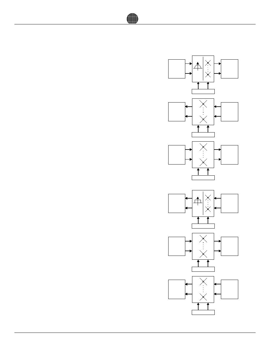
FUNCTIONAL DESCRIPTION
The DSP24 is the latest generation of real time
DSP designed to facilitate the handling of fast real time
digital signals with a minimum of software overhead.
The DSP24 is organized into five major groups:
"
Input and Output Data Ring Buses
"
Core Logic
"
Internal Memories
"
Scheduler/Controller
"
These major groups work in tandem to acquire
complex or real data, apply functions on the acquired
arrays of data, and store results both internally and
externally for further processing, or output.
INPUT AND OUTPUT RING BUSSES
Data enters the DSP24 through any of its five
complex data ports and exits the DSP24 through any of
its complex five ports.
The internal ring busses give the user complete
control on which port to input operands from and which
ports to output the results through. This elaborate
internal structure frees the end user from virtually any
need to multiplex data external to the DSP24.
Additionally the five ports can be used to seamlessly
cascade multiple chips as illustrated in the System
C
onfigurations section.
CORE LOGIC
The internal data path is designed to execute Fast
Fourier Transforms (FFTs) with efficiency and precision.
The core is will execute thirty four high level
functions on the incoming data. Functions as
sophicated as radix-1024 are performed at the full data
rate.
Each input complex pair of data id operated upon
by the core using a super pipelined approach. This
approach allows many operations to be performed on
Control Inputs
each clock cycle.
The acquired array of complex or real data may be
passes through the core logic multiple times for
execution of complete algorithms such as fast adaptive
digital filtering without the data having ever left the chip
until the final output pass.
The core logic reconfigures itself transparent to the
user to facilitate unique parallel processing
configurations that can command the needed
performance to execute a 1024 point by 1024 point
complex 2-D FFT at a 100 MHz sample rate sustained,
when four chips are used.
INTERNAL MEMORIES
The DSP24 contains two banks of internal memory
organized as 1024 words by 48 bits each.
This memory is used to cascade multiple chips and
to provide user storage of sampled data when arrays
sizes are less than 1024 complex words (24 bits real
plus 24 bits imaginary.
As an example, the user may acquire 1024
complex words from a buffered analog-to-digital
converter, as shown back in Figure 1. During the
acquisition pass from Port A, a radix-32 FFT may be
performed while the data is passing through the Logic
Core into the internal A memory array.
The next defined pass, if fast convolution (digital
filtering) were being performed would be an inverse
FFT with the complex data coming from the same
memory A.
Cascading of DSP24 chips for more functionally
and higher sampled data rates uses the internal
memories to store computed FFT columns before
passing the complex data to the next chip connected to
the output pins. See the System Configurations
section.
Through proper use of the internal memories,
complete real time systems may be scaled up or down
in performance by adding multiple ASIC silicon DSP24
cores on one die, by cascading multiple multiple die in
one multi-chip module (MCM), by parallelizing multiple
packaged chips on a board, or by parallelizing multiple
boards in a unit.
SCHEDULER/CONTROLLER
To enable complete real time systems with minimum
effort, the DSP24 contains all the circuitry to implement
a robust application controller. The
SCHEDULER/CONTROLLER maintains the users
application by sourcing a series of instructions for the
DSP24 itself and for any Memory Management Units
DSP24
Digital Signal Processor
DSP
Architectures

Data Sheet
Page 15
Digital Signal Processor
DSP24
DSP
Architectures
SCHEDULER/CONTROLLER (cont.)
The SCHEDULER/CONTROLLER plays a dual role
in the overall system operation. Its primary role
involves synchronously scheduling the events
needed to perform demanding real time signal
processing. This scheduling essentially takes the
user provided program as it exists in the external
PROM and parses it to both the internal MMU and
the internal DSP controllers.
The SCHEDULER/CONTROLLER's secondary role
is to program both the DSP24 and any MMU-24's
that reside in the system. These controllers provide a
robust structure for efficient operation of all the
resources in a typical real time system, including
systems that contain multiple DSP24's for increased
performance.
Figure 4. illustrates the SCHEDULER, both internal
CONTROLLERS, and the required external program
PROM.
CONTROL INPUTS
For increased system flexibility, the user may select
between using the internal
SCHEDULER/CONTROLLER and supplying the
necessary control signals himself. This option is
exercised through either grounding the SCHSEL
input pin, or connecting the SCHSEL pin to VCC.
If SCHSEL is grounded, the user will be required to
manage the signals shown in Figure 5.
Note: Most of the signal pins shown in Figure 5 are
dual function pins whose function depend on the
state of the SCHSEL pin.
Data Sheet
Page 16
SCH DB[7:0]
ADDR[15:0]
ADDREN
SCHEDULER
MMU
CONTROLLER
MMUCSD
MMUCSE
MMUCSC
MMUCSB
MMUCSA
MMU START
MMU A1
MMU A0
MMU R/W
MMU RESET
SSYNC [1:0]
BUSY
Figure 4. SCHEDULER/CONTROLLER
EXTERNAL
PROM
To Memory Management Units
XSFISEL
DOCI
ENB
DOCR
DZO
XSWAP
ENA
XCR
YZI
DF[8:0]
XCI
XZI
FC[5:0]
YSFI[3:0]
YCR
XSFI[3:0]
YCI
START/STOP
RESET
DSP
CONTROLLER
Internal
Signals
when
SCHSEL
is active
GO[1:0]
MMUTCE
MMUTCD
MMUTCC
MMUTCB
MMUTCA
SCHSEL
ALG[7:0]
CS
+
DSP24
Digital Signal Processor
(MMU-24s)
DSP
Architectures
Data Sheet
Page 17
Figure 5. DSP24 Control/ Sync
Internal
Chip Decodes
Internal
Chip Decodes
Internal
Chip Decodes
REG
A
REG
B
SYSCLKEN
START/STOP
RESET
DZO
YZI
PI[1:0]
YSWAP
XZI
XSWAP
BFPI[5:0]
YCR
YCI
YSFI[3:0]
XSFI[3:0]
XSFISEL
ENB
ENA
DF[8:0]
FC[5:0]
SYNCIN[1:0]
SYNCOUT[1:0]
SYSCLK
XCI
BFPO[5:0]
ERROR
DOCR
XCR
SFO[3:0]
DOCI
Variable Length Shift Register
Digital Signal Processor
DSP24
DSP
Architectures

Data Sheet
Page 18
DATA FORMATS
INPUT/OUTPUT DATA FORMATS
The DSP24 supports (2) two input data streams:
one for real and one for imaginary data. For CMAG
and
FIR operations, the 48-bit output from each ALU accu-
mulation is rounded to 48 bits and output from the
DSP24, Most-Significant-Word first, in two clock
cycles, one on the real side and one on the imaginary
side. All other outputs are rounded up to 24 bits.
BLOCK FLOATING-POINT
For the radix butterfly transform operations, block
floating-point data dependent scaling is provided. This
preserves the signal-to-noise ratio by extending the
dynamic range of the fixed-point operations.
For each pass of an FFT, or on a separation pass,
a scale factor is provided on the DSFO [2:0] pins at the
completion of that pass. The scale factor is a binary
shift number calculated from the size of the largest
complex value output in that pass. Also, it is a worst
case prediction of how large the magnitude of the
largest
complex value could be on the next pass. The
magnitude is measured for each complex value output
in the pass. The maximum magnitude is compared to
many threshold values. If the magnitude is gr eater, the
corresponding shift value (from an internal lookup
table)
is output on DSFO [3:0]. It is used at the beginning of
the next pass on the XSFI [3:0] pins and causes a right
shift of the real and imaginary 24-bit inputs to prevent
overflow on the pass.
The BFPO [5:0] is the accumulated scale factor for
the entire transform and is valid upon the transform's
completion. The BFPO and BFPI pins should be con-
nected together for single and parallel chip
applications,
or connected serially for cascaded operations.
ROUNDING/SHIFTING OPERATION
All data input to the DSP24 passes through a
shifter and rounder at both the input and output stages.
The amount of shifting and rounding is determined by
the current instruction. To correctly scale the incoming
data, the shifter is capable of shifting up to (16) sixteen
DSFI bit positions to the right. The rounder trims the
data to the necessary 24 bits needed by monitoring the
25th bit (1/2 of the LSB) and adding:
Fractional
XXXXXXX
Rounding
+ 0000008
XXXXXXX
When bit 25 is set, the output is rounded up, other-wise
the data is not rounded.
THEORY OF OPERATION
FUNCTION SET OVERVIEW
The DSP24 is a high-performance array processor
designed to perform operations on large arrays of
data. Accordingly, the DSP24 has a powerful function
set in the sense that each function opcode
accomplishes a substantial task. The following are
some
key points about the DSP24 function set.
"
Since the DSP24 is a pass-based processor,each
function is valid for one complete pass. Each
opcode defines a basic flow for the desired
operation. This basic data flow is then repeated for
multiple pairs of data to complete one pass.
"
Each function is qualified by the START/STOP
signal to indicate the beginning of a pass and end
of a pass respectively.
"
The Transform functions can also be qualified by
DZI and DZO signals which, when asserted, cause
the DSP24 to input a string of zeros and force
output data to zeros respectively. This feature
allows a user to zero fill and zero pad the data on
any given pass.
"
The DSP24 function set consist of five functional
groupings. A 6-bit opcode is assigned to each
function, with a total of thirty-four functions
supported. The function code on the pins FC[ 5:0]
must be setup at least three machine cycles ahead
of data setup. This allows the automatic scaling
factor to be decoded for the next pass. For a
typical array processing application, such as FFTs,
first a function code is set up (e.g., BFLY32),and
then the whole data array is clocked into the
DSP24. The applied function will then be applied to
the whole array.
"
There is a latency, given in machine cycles when
implementing the DSP24 functions (see Table 4.)
This latency is automatically compensated for
when the MMU-24 is used in a system.
DSP24
Digital Signal Processor
DSP
Architectures
Data Sheet
Page 19
THEORY OF OPERATION (cont.)
FUNCTION SET OVERVIEW (cont.)
There are provisions, useful for implementing inverse
FFTs, to conjugate the inputs to, and the outputs from,
the complex arithmetic functions (pins DCI and DCO).
Similarly, the input and output data values can be com-
plemented for the vector arithmetic and logical functions.
The DSP24 also includes a PASS general purpose
function, this function moves data and coefficients between
ports and through the execution unit without altering their
value.
INPUT/OUTPUT DATA FLOW
Data input to and output from the DSP24 depends
upon the data flow function given (reference Table 3).
TWO REAL TRANSFORMS (BRFT)
The BRFT function may be used to process two
frames of real-data simultaneously and obtain almost
twice the performance while still using a complex data
FFT. Given two real sequences, h(n) and g(n), they can
be concatenated and represented as a complex
sequence, such as: x(n) = h(n) + jg(n).
To compute the BRFT do the following:
1. Functions h(k) and g(k) are real
k = 0, 1, ..., N - 1
2. Form the complex function
y(k) = h(k) + jg(k) k = 0, 1, ..., N - 1
3. Compute the FFT
= R(n) + jI
(n) n = 0, 1, ..., N - 1
where R(n) and l(n) are the real and imaginary parts
of Y(n), respectively.
4. Compute the separation
n = 0,
1, ..., N - 1
where H(n) and G(n) are the discrete transforms of
h(k) and g(k), respectively.
DOUBLE LENGTH RECOMBINATION OF
FFT OUTPUT (BFCT)
This pass performs both a fast cosine transform
recombination and a double length separation.
Double Length Separation separates a 2N length
real FFT from a N length complex FFT as follows:
1. Function x(k) is real
k = 0,
1, ..., 2N - 1
2. Divide x(k) into two functions
h(k)
= x(2k)
g(k) = x(2k +
1) k = 0, 1, ..., N - 1
3. Form the complex function
y
(k) = h(k) + jg(k) k = 0, 1, ..., N - 1
4. Compute the FFT
= R(n) + jI
(n) n = 0, 1, ..., N - 1
where R(n) and l(n) are the real and imaginary parts
of Y(n), respectively.
5. Compute the separation
where x
r
(n) and x
i
(n) are respectively the real and
imaginary parts of the 2N point discrete transform of
x(k).
NOTES:
1. Only N points of the real output are unique, and the
imaginary output will be zero since the input function
is an even, real only function.
2. The DSP24 does not perform the division by two
in the BRFT, BFCT, and BFCT2 functions. This was
done to allow the user to perform the division by two, if
so decided.
H(n)=
G(n)=
R(n)
R(N-n)
2
2
+
R(n)
R(N-n)
2
2
-
I(n)
I(N-n)
2
2
+
I(n)
I(N-n)
2
2
-
+j
-j
n=0, 1,....., N-1
R(n)
R(N-n)
2
2
+
I(n)
I(N-n)
2
2
-
R(n)
R(N-n)
2
2
-
R(n)
R(N-n)
2
2
-
I(n)
I(N-n)
2
2
+
I(n)
I(N-n)
2
2
+
Xr(n) =
Xi(n) =
n= 0, 1,....,N-1
n= 0, 1,....,N-1
+ cos
- sin
- sin
- cos
n
n
n
n
N
N
N
N
Y(n)=
N-1
k=0
y(k)e-j2 nk/N
Y(n)=
N-1
k=0
y(k)e-j2 nk/N
Digital Signal Processor
DSP24
DSP
Architectures
Data Sheet
Page 20
SYSTEM OVERVIEW
The DSP24 incorporates a unique architecture
optimized for extremely high data throughput and minimal
hardware/software system development. For the digital filter
example of Figure 7, do a 4096 point forward FFT, a
multiplication, and an inverse FFT, using the following
program.
BWND4 +Window Column 1
BFLY32 Column 2
BFLY32 Column 3
Conjugate Input BWND4 + Complex multiply Column 4
BFLY32 Column 5
Conjugate Output BFLY32 Column 6
For a 4K transform, there are three columns using
the radix-4 and radix-32 operations. Each column represents
one "pass". A "pass" is transferring data from
one memory bank (AB,C,D, or E), through the machine to the
other memory bank (A, B, C, D, E, or F). During each pass the
DSP24 performs a DSP function on the data using coefficients
from the coefficient port, if necessary.
As shown in Figure 7 the data is first input through DSP24 and
a window function is combined with the first column of the
FFT.
Next the data is passed a second time through the DSP24
performing a radix32 operation, the third pass back through
the DSP24 another radix32 operation is performed. This
completes the forward FFT including the window function
multiply.
For the forth through the sixth passes through the DSP24 this
three pass operation is repeated with the window function
being replaced with the desired filter coefficients, also the data
on the fourth pass is conjugated on the input side and the data
on the sixth pass is conjugated on the output side.
This approach to real time DSP can be proportionally
accelerated by adding multiple DSP24's in the data flow, the
following section on system configurations illustrate this.
INPUT
DATA
INPUT
DATA
INPUT
DATA
INPUT
DATA
INPUT
DATA
INPUT
DATA
COLUMN
1
COLUMN
4
COLUMN
2
COLUMN
5
COLUMN
3
COLUMN
6
DSP24
DSP24
DSP24
DSP24
DSP24
DSP24
Twiddles
Window
Twiddles
Filter
Twiddles
Twiddles
Figure 7
BWND4
BFLY32
BFLY32
BWND4
BWND32
BWND32
DSP24
Digital Signal Processor
DSP
Architectures
Data Sheet
Page 21
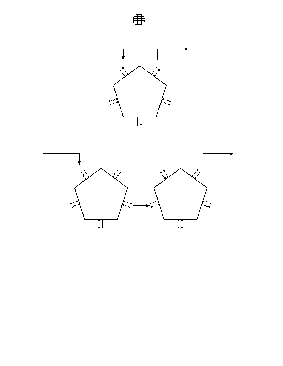
For several applications, the DSP24 may be used alone
without external components as shown in Figure 8a.
This configuration will perform a 1024 point complex
FFT in just two passes, for a continuous sampling rate of
50 MHz complex.
The 50 MHz performance may be scaled up to 100 MHz
by simply adding another DSP24 die in the package or
two packaged chips back to back, see Figure 8b.
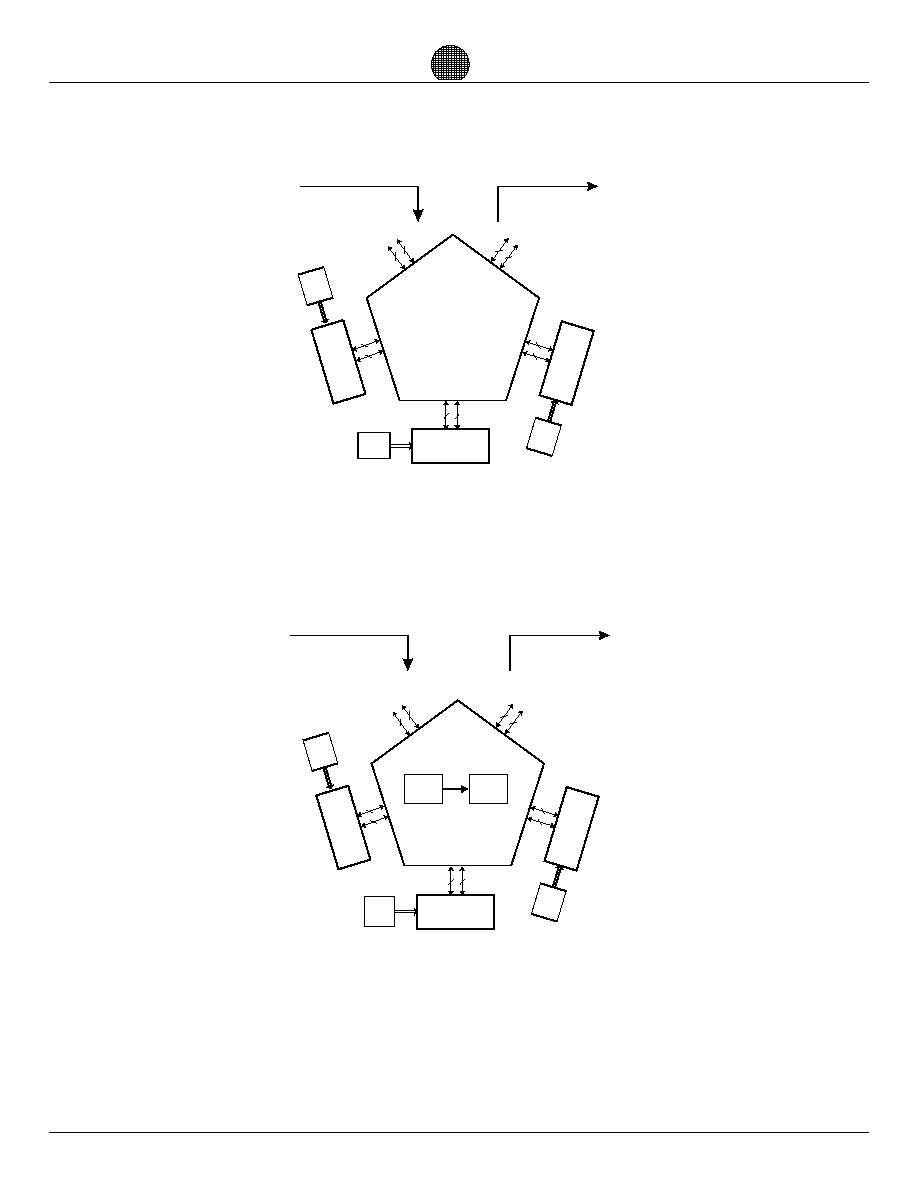
For larger arrays, external memories and external
Memory Management Units (MMU-24s) may be
required, as shown in Figure 9a. The addition of these
simple external devices will support arrays up to 1
million complex points.
Again two packaged chips, or two die may be cascaded
back to back as shown in Figure 9b to increase
performance.
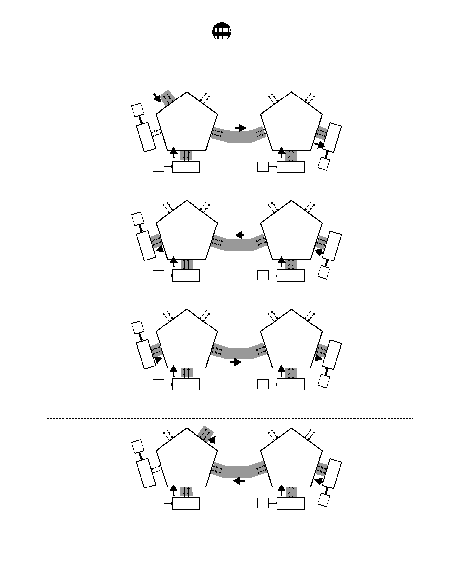
Figure 10 shows the four data flow phases required for
two DSP24 chips performing a four pass operation such
as a 2-D 1024 point complex FFT followed by a 2-D
1024 point inverse complex FFT.
As shown in Figure 10a data enters port A of the
first DSP24 #1 along with the required twiddle
factors through port D. This data is processed
through the core logic of DSP24 #1 and passes out
of port C to the input port E of DSP24 #2.
The data then exits DSP24 #2 through port C into
the memory connected to port C. This completes
the first of four passes.
The second, third, and fourth passes of the
algorithm are shown in Figure 10b, 10c, and 10d
respectfully. The data is ping ponged in this fashion
for the total required number of passes.
SYSTEM CONFIGURATIONS
INPUT
50 MHz
Complex
OUTPUT
50 MHz
Complex
INPUT
100 MHz
Complex
OUTPUT
100 MHz
Complex
PORT A
PORT B
PORT C
PORT D
PORT E
24
24
24
24
24
24
24
24
24
24
PORT A
PORT B
PORT C
PORT D
PORT E
24
24
24
24
24
24
24
24
24
24
PORT A
PORT B
PORT C
PORT D
PORT E
24
24
24
24
24
24
24
24
24
24
Figure 8b
Figure 8a
Digital Signal Processor
DSP24
DSP
Architectures
Data Sheet
Page 22
INPUT
OUTPUT
100 MHz/# of passes
Complex
100 MHz/# of passes
Complex
SRAM
MMU
M
U
M
S
M
A
R
R
S
A
M
M
M
U
PORT A
PORT B
PORT C
PORT D
PORT E
24
24
24
24
24
24
24
24
24
24
INPUT
OUTPUT
50 MHz
Complex
50 MHz
Complex
SRAM
MMU
M
M
U
M
R
A
S
M
S
R
A
M
M
U
PORT A
PORT B
PORT C
PORT D
PORT E
24
24
24
24
24
24
24
24
24
24
DIE 1
DIE 2
Figure 9a
Figure 9b
DSP24
Digital Signal Processor
DSP
Architectures
Data Sheet
Page 23
Digital Signal Processor
DSP24
SRAM
MMU
M
U
M
S
R
A
M
PORT A
PORT B
PORT C
PORT D
PORT E
24
24
24
24
24
24
24
24
24
24
SRAM
MMU
R
M
A
S
M
U
M
PORT A
PORT B
PORT C
PORT D
PORT E
24
24
24
24
24
24
24
24
24
24
DSP24
1
DSP24
2
SRAM
MMU
M
U
M
M
S
R
A
PORT A
PORT B
PORT C
PORT D
PORT E
24
24
24
24
24
24
24
24
24
24
SRAM
MMU
R
M
A
S
M
M
U
PORT A
PORT B
PORT C
PORT D
PORT E
24
24
24
24
24
24
24
24
24
24
DSP24
1
DSP24
2
SRAM
MMU
M
U
M
R
S
A
M
PORT A
PORT B
PORT C
PORT D
PORT E
24
24
24
24
24
24
24
24
24
24
SRAM
MMU
M
R
S
A
M
U
M
PORT A
PORT B
PORT C
PORT D
PORT E
24
24
24
24
24
24
24
24
24
24
DSP24
2
DSP24
1
SRAM
MMU
M
U
M
S
R
A
M
PORT A
PORT B
PORT C
PORT D
PORT E
24
24
24
24
24
24
24
24
24
24
SRAM
MMU
R
M
A
S
M
U
M
PORT A
PORT B
PORT C
PORT D
PORT E
24
24
24
24
24
24
24
24
24
24
DSP24
1
DSP24
2
Figure 10a Phase 1
Figure 10b Phase 2
Figure 10c Phase 3
Figure 10d Phase 4
Window and first radix-32 column (VWND32)
Second radix-32 column (BFLY32)
Third radix-32 column (BFLY32)
Fourth radix-32 column (BFLY32)
Combined filter multiply and first radix-32 IFFT
(VWND32) column
Second radix-32 column (BFLY32)
Third radix-32 column (BFLY32)
Fourth radix-32 column (BFLY32)
Figure 10 2-D Complex 1K x 1K Fast Convolution
DSP
Architectures
Data Sheet
Page 24
Figure 11a
Cascading Four Chips, Phase one
Figure 11b
Cascading Four Chips Phase two
48
48
48
Memory A
Memory B
Logic Core
Scheduler/
Controller
System
Controls
PROM
Interface
PORT E
PORT D
PORT C
PORT B
PORT A
Control
24
24
24
24
24
24
24
24
24
24
24
24
24
24
24
24
24
24
24
24
48
48
48
Memory A
Memory B
Logic Core
Scheduler/
Controller
System
Controls
PROM
Interface
PORT E
PORT D
PORT C
PORT B
PORT A
Control
24
24
24
24
24
24
24
24
24
24
24
24
24
24
24
24
24
24
24
24
48
48
48
Memory A
Memory B
Logic Core
Scheduler/
Controller
System
Controls
PROM
Interface
PORT E
PORT D
PORT C
PORT B
PORT A
Control
24
24
24
24
24
24
24
24
24
24
24
24
24
24
24
24
24
24
24
24
48
48
48
Memory A
Memory B
Logic Core
Scheduler/
Controller
System
Controls
PROM
Interface
PORT E
PORT D
PORT C
PORT B
PORT A
Control
24
24
24
24
24
24
24
24
24
24
24
24
24
24
24
24
24
24
24
24
S
R
A
M
Up tp 100 MSPS
Continuous
Data
Input
Up to 100 MSPS
Continuous
Data
Output
ROM
MMU-24
ROM
MMU-24
S
R
A
M
MMU-24
MMU-24
48
48
48
Memory A
Memory B
Logic Core
Scheduler/
Controller
System
Controls
PROM
Interface
PORT E
PORT D
PORT C
PORT B
PORT A
Control
24
24
24
24
24
24
24
24
24
24
24
24
24
24
24
24
24
24
24
24
48
48
48
Memory A
Memory B
Logic Core
Scheduler/
Controller
System
Controls
PROM
Interface
PORT E
PORT D
PORT C
PORT B
PORT A
Control
24
24
24
24
24
24
24
24
24
24
24
24
24
24
24
24
24
24
24
24
48
48
48
Memory A
Memory B
Logic Core
Scheduler/
Controller
System
Controls
PROM
Interface
PORT E
PORT D
PORT C
PORT B
PORT A
Control
24
24
24
24
24
24
24
24
24
24
24
24
24
24
24
24
24
24
24
24
48
48
48
Memory A
Memory B
Logic Core
Scheduler/
Controller
System
Controls
PROM
Interface
PORT E
PORT D
PORT C
PORT B
PORT A
Control
24
24
24
24
24
24
24
24
24
24
24
24
24
24
24
24
24
24
24
24
S
R
A
M
Up tp 100 MSPS
Continuous
Data
Input
Up to 100 MSPS
Continuous
Data
Output
ROM
MMU-24
ROM
MMU-24
S
R
A
M
MMU-24
MMU-24
SYSTEM CONFIGURATIONS
(cont.)
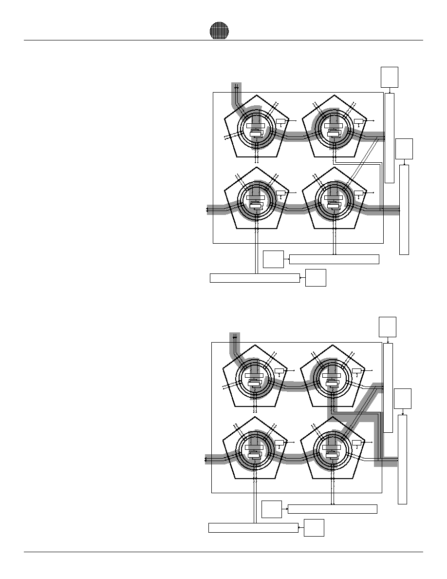
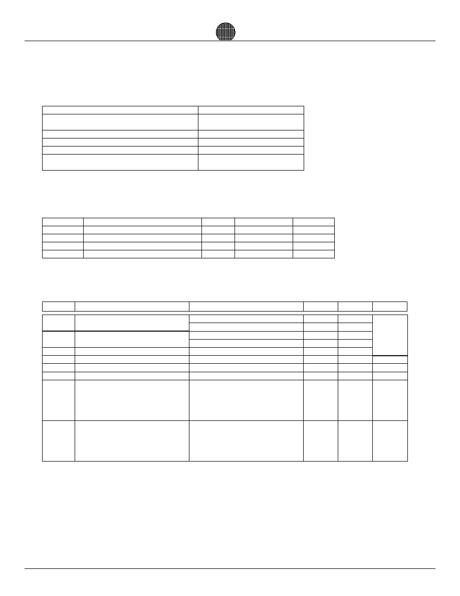
Cascading four DSP24's yields an impressive
100 MSPS complex FFT with 1 million complex
points of resolution, or a 1024x1024 two-
dimension(2-D) transform in 20 milliseconds.
Figure 11 shows a Multi-Chip Module (MCM)
with four DSP24 die connected back to back.
As illustrated in Figure 11a, phase one runs all
four die concurrently with the top two chips
performing 1024 of the required 1024 point
complex FFT's and storing the result in an
external 1 million point RAM. While this is
taking place the bottom two chips in the MCM
are taking the results from a previous pass and
also performing 1024 of the required 1024
point complex FFT's for the final output.
Figure 11b shows the second phase of this
concurrent process with the chip pairs
swapping working memories, this allows real
time processing in a seamless pipelined
fashion.
DSP24
Digital Signal Processor
DSP
Architectures
Data Sheet
Page 25
DC Voltage Applied to Outputs in High-Z State
Power Dissipation (Package Limit)
Storage Temperature range
DC Output Current
Signal Pin Voltage to VSS Potential
Supply Voltage to VSS Potential
DC ELECTRICAL CHARACTERISTICS
Excludes output load current.
Excludes output load current.
All inputs = VIL (0.3 VDD),
All inputs = VIL (0.3 VDD),
Measured at tcyc (100MHz)
IOL=6.0 mA
IOH=-6.0 mA
VDD=3.13 V, VIN= 0 to VDD
VIN=VSS
VDD=3.13, VIN=VDD
VIN=VDD
VDD=3.13 V, VIN=0 V
Quiescent Standby Current
Average Standby Current
Average Supply Current
Output Low Voltage
Output High Voltage
Input Leakage Current
Pull-Down Input Leakage
Current
I
LPUI
I
LPDI
I
LI
V
OL
V
LOH
I
DDI
I
DD2
I
DD3
2.4
-10
-10
15
-10
-70
uA
V
V
mA
mA
mA
10
10
70
10
-15
1
1200
0.26
1
SYMBOL
DESCRIPTION
TEST CONDITIONS
MIN
MAX
UNIT
6
7
ABSOLUTE MAXIMUM RATINGS
(not to exceed 5 V)
-0.3 to VDD +0.3 V
18 W
-40 deg C to 125 deg C
10 mA
(not to exceed 5 V)
-0.3 to VDD +0.3 V
-0.3 V to 5V
OPERATING RANGE
TA
VDD
VSS
VIL
VIH
Temperature, Ambient
Supply Voltage
Supply Voltage
Logic '0' Input Voltage
Logic '1' Input High Voltage
0.3 VDD
0.7 VDD
0.0
3.13
0
VDD+0.3
0.0
3.43
70
deg C
V
V
V
V
+
-
MIN
UNIT
MAX
1
1,2
1
See notes on Page 26
(Over Operating Range)
5
Digital Signal Processor
DSP24
DSP
Architectures
Data Sheet
Page 26
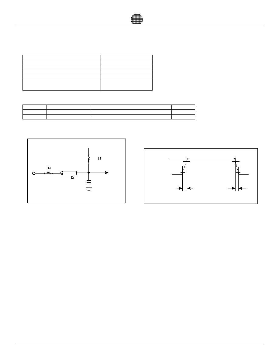
Figure 12a. Output Load Circuit
Figure 12b. Input Rise and Fall Times
VSS
3.0 VDDV
1.5ns
1.5ns
10%
90%
90%
10%
DSP24
100
67
100
35 pf
DSP24
1.0 V
AC TEST CONDITIONS
Input Pulse levels
Input Rise & Fall Times (10% to 90%)
Input Timing Reference Levels
Output Reference Levels
Output Load, Timing Tests
Figure 16b
0.35 VDD
0.35 VDD
(Figure 16a)
1.5 ns
VSS to 3.0 VDD
PARAMETER
RATING
COUT
CIN
Input Capacitance
Output Capacitance
TA=25 deg C, F=1MHz, VDD=3.13 V 10 pF
TA=25 deg C, F=1MHz, VDD=3.13 V 10 pF
RATING
TEST CONDITIONS
DESCRIPTION
SYMBOL
CAPACITANCE
1. All voltages are measured with respect to VSS.
2. Stresses greater than those listed under 'Absolute
Maximum Ratings' may cause permanent damage to
the device. This is a stress rating for transient
conditions only. Functional operation of the device at
these or any other conditions above those indicated
in the ' Operating Range' of this specification is not
implied.
Exposure to absolute maximum rating conditions for
extended periods may affect reliability.
3. Outputs should not be shorted for more than 30
seconds. No more than one output should be
shorted at any time.
4. Sample tested only
5. The DSP24 inputs are able to withstand a -
1.0V undershoot for less than 10 ns per cycle.
6. An internal pull-up resistor is attached to all
the data bus pins : AR[23:0], AI[23:0],
BR[23:0], BI[23:0], CR[23:0], CI[23:0],
DR[23:0], DI[23:0], ER[23:0], EI[23:0].
7. An internal resistor is attached to all the
non-bus signals to bias them inactive when not
physically connected at the board level.
8. IDD is dependent upon actual output
loading and cycle rates. Specific values are
with outputs open.
NOTES:
INCLUDES JIG AND SCOPE CAPACITANCES
1
1,4
DSP24
Digital Signal Processor
DSP
Architectures
Data Sheet
Page 27
CYC
CL
CH
SCLKEN
HCLKEN
RESET
SKT
DSA
DHA
DODA
DOHA
LZOEA
HZOEA
DSB
DHB
DODB
DOHB
LZOEB
HZOEB
DSC
DHC
DODC
DOHC
LZOEC
HZOEC
DSD
DHD
DODD
DOHD
LZOED
HZOED
DSE
DHE
DODE
DOHE
LZOEE
HZOEE
SA
HA
SCTLA
HCTLA
SB
HB
SCTLB
HCTLB
SCTLC
HCTLC
ODCTL
SBFPC
HBFPC
SSTART
HSTART
SSYNC
HSYNC
DODSYNC
DODPOUT
DODERR
SKL
SYSCLK Cycle Time
Clock Low Time (SYSCLK)
Clock High Time (SYSCLK)
SYSCLKEN Setup Time (SYSCLK)
SYSCLKEN Hold Time (SYSCLK)
RESET High Time
CLKxIN to SYSCLK, Rising Edge to Rising Edge Skew
SYSCLK to CLKxIN, Rising Edge to Rising Edge Skew
AR[23:0], AI[23:0] Setup Time (CLKAIN)
AR[23:0], AI[23:0] Hold Time (CLKAIN)
AR[23:0], AI[23:0] Output Delay Time (SYSCLK)
AR[23:0], AI[23:0] Output Hold Time (SYSCLK)
AOE High to AR[23:0], AI[23:0] Low-Z
AOE Low to AR[23:0], AI[23:0] High-Z
BR[23:0], BI[23:0] Setup Time (CLKBIN)
BR[23:0], BI[23:0] Hold Time (CLKBIN)
BR[23:0], BI[23:0] Output Delay Time (SYSCLK)
BR[23:0], BI[23:0] Output Hold Time (SYSCLK)
BOE High to BR[23:0], BI[23:0] Low-Z
BOE Low to BR[23:0], BI[23:0] High-Z
CR[23:0], CI[23:0] Setup Time (CLKCIN)
CR[23:0], CI[23:0] Hold Time (CLKCIN)
CR[23:0], CI[23:0] Output Delay Time (SYSCLK)
CR[23:0], CI[23:0] Output Hold Time (SYSCLK)
COE High to CR[23:0], CI[23:0] Low-Z
COE Low to CR[23:0], CI[23:0] High-Z
DR[23:0], DI[23:0] Setup Time (CLKDIN)
DR[23:0], DI[23:0] Hold Time (CLKDIN)
DR[23:0], DI[23:0] Output Delay Time (SYSCLK)
DR[23:0], DI[23:0] Output Hold Time (SYSCLK)
DOE High to DR[23:0], DI[23:0] Low-Z
DOE Low to DR[23:0], DI[23:0] High-Z
ER[23:0], EI[23:0] Setup Time (CLKEIN)
ER[23:0], EI[23:0] Hold Time (CLKEIN)
ER[23:0], EI[23:0] Output Delay Time (SYSCLK)
ER[23:0], EI[23:0] Output Hold Time (SYSCLK)
EOE High to ER[23:0], EI[23:0] Low-Z
EOE Low to ER[23:0], EI[23:0] High-Z
ENA Setup Time (SYSCLK)
ENA Hold Time (SYSCLK)
FC[5:0], DF[8:0] Setup Time (SYSCLK)
FC[5:0], DF[8:0] Hold Time (SYSCLK)
ENB Setup Time (SYSCLK)
ENB Hold Time (SYSCLK)
XSFISEL, XSFI[3:0], YSFI[3:0], BFPI[5:0], XCR, XCI, DOCR, DOCI
Setup
XSFISEL, XSFI[3:0], YSFI[3:0], BFPI[5:0], XCR, XCI, DOCR, DOCI
Hold
XZI, YZI, DZO, YCR, YCI, YSWAP, XSWAP Setup (SYSCLK)
XZI, YZI, DZO, YCR, YCI, YSWAP, XSWAP Hold (SYSCLK)
BFPO[5:0], DSFO[3:0] Output Delay Time (SYSCLK)
BFPCLR Setup Time (SYSCLK)
BFPCLR Hold Time (SYSCLK)
START/STOP Setup Time (SYSCLK)
START/STOP Hold Time (SYSCLK)
SYNCIN[1:0] Setup Time (SYSCLK)
SYNCIN[1:0] Hold Time (SYSCLK)
SYNCOUT[1:0] Output Delay Time (SYSCLK)
POUT[2:0] Output Delay Time (SYSCLK)
ERROR Output Delay Time (SYSCLK)
t
t
t
t
t
t
t
t
t
t
t
t
t
t
t
t
t
t
t
t
t
t
t
t
t
t
t
t
t
t
t
t
t
t
t
t
t
t
t
t
t
t
t
t
t
t
t
t
t
t
t
t
t
t
t
t
t
t
ns
ns
ns
ns
ns
ns
ns
ns
ns
ns
ns
ns
ns
ns
ns
ns
ns
ns
ns
ns
ns
ns
ns
ns
ns
ns
ns
ns
ns
ns
ns
ns
ns
ns
ns
ns
ns
ns
ns
ns
ns
ns
ns
ns
ns
ns
ns
ns
ns
ns
ns
ns
ns
ns
ns
ns
ns
ns
9
9
9
9
9
9
9
9
9
9
8
8
8
8
8
10
5
5
6
0
20
1.5
1.5
6
0
7
2
6
0
7
2
6
0
7
2
6
0
7
2
6
0
7
2
6
0
6
0
6
0
6
0
6
0
6
0
6
0
6
0
7
8
8
8
8
8
8
8
8
8
8
7
7
7
7
12.5
6.25
6.25
7
0
20
2
2
7
0
8
3
7
0
8
3
7
0
8
3
7
0
8
3
7
0
8
3
7
0
7
0
7
0
7
0
7
0
7
0
7
0
7
0
AC ELECTRICAL CHARACTERISTICS
SIGNAL
DESCRIPTION
MIN
MIN
TYP
TYP
UNIT
MAX
MAX
80 MHz
100 MHz
Digital Signal Processor
DSP24
DSP
Architectures
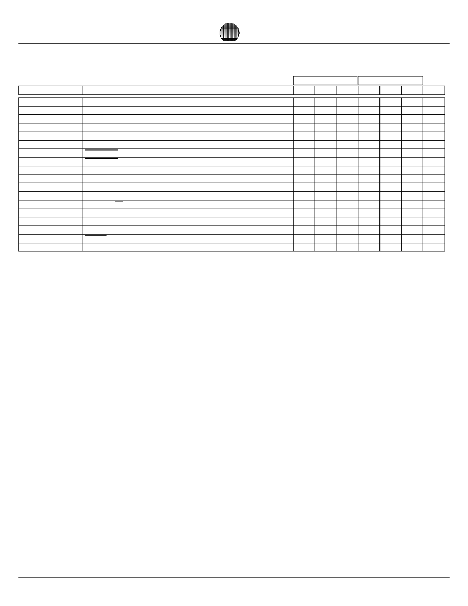
Data Sheet
Page 28
SSCH
HSCH
SGO
HGO
STC
HTC
HZADDR
LZADDR
ODADDR
SSDB
HSDB
ODMRESET
ODRW
ODA0
ODSTART
ODCS
ODBUSY
ODSSYNC
SCHSEL Setup Time (SYSCLK)
SCHSEL Hold Time (SYSCLK)
GO[1:0] Setup Time (SYSCLK)
GO[1:0] Hold Time (SYSCLK)
MMU_TC_A, _B, _C, _D, _E Setup Time (SYSCLK)
MMU_TC_A, _B, _C, _D, _E Hold Time (SYSCLK)
ADDREN High to ADDR[15:0] High-Z
ADDREN Low to ADDR[15:0] Low-Z
ADDR[15:0] Output Valid Delay Time (SYSCLK)
SCHDB[7:0] Setup Time (SYSCLK)
SCHDB[7:0] Hold Time (SYSCLK)
MMU_RESET Output Delay Time (SYSCLK)
MMU_R/W Output Delay Time (SYSCLK)
MMU_A0 Output Delay Time (SYSCLK)
MMU_START Output Delay Time (SYSCLK)
MMU_CS_A, B, C, D, E Output Delay Time (SYSCLK)
BUSY Output Delay Time (SYSCLK)
SSYNC[1:0] Output Delay Time (SYSCLK)
t
t
t
t
t
t
t
t
t
t
t
t
t
t
t
t
t
t
ns
ns
ns
ns
ns
ns
ns
ns
ns
ns
ns
ns
ns
ns
ns
ns
ns
ns
9
9
8
8
8
8
8
8
8
8
8
6
0
6
0
6
0
6
0
7
8
8
7
7
7
7
7
7
7
7
7
0
6
0
7
0
7
0
AC ELECTRICAL CHARACTERISTICS
SIGNAL
DESCRIPTION
MIN
MIN
TYP
TYP
UNIT
MAX
MAX
80 MHz
100 MHz
DSP24
Digital Signal Processor
Note: All clocks signals (CLKxIN, SYSCLK) must be driven, or grounded if not used
DSP
Architectures
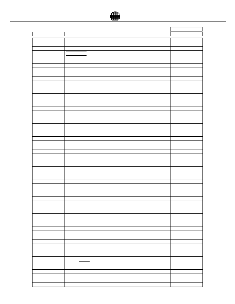
Data Sheet
Page 29
CYC
CL
CH
SCLKEN
HCLKEN
RESET
SKT
DSA
DHA
DODA
DOHA
LZOEA
HZOEA
DSB
DHB
DODB
DOHB
LZOEB
HZOEB
DSC
DHC
DODC
DOHC
LZOEC
HZOEC
DSD
DHD
DODD
DOHD
LZOED
HZOED
DSE
DHE
DODE
DOHE
LZOEE
HZOEE
SA
HA
SCTLA
HCTLA
SB
HB
SCTLB
HCTLB
SCTLC
HCTLC
ODCTL
SBFPC
HBFPC
SSTART
HSTART
SSYNC
HSYNC
DODSYNC
DODPOUT
DODERR
SKL
SYSCLK Cycle Time
Clock Low Time (SYSCLK)
Clock High Time (SYSCLK)
SYSCLKEN Setup Time (SYSCLK)
SYSCLKEN Hold Time (SYSCLK)
RESET High Time
CLKxIN to SYSCLK, Rising Edge to Rising Edge Skew
SYSCLK to CLKxIN, Rising Edge to Rising Edge Skew
AR[23:0], AI[23:0] Setup Time (CLKAIN)
AR[23:0], AI[23:0] Hold Time (CLKAIN)
AR[23:0], AI[23:0] Output Delay Time (SYSCLK)
AR[23:0], AI[23:0] Output Hold Time (SYSCLK)
AOE High to AR[23:0], AI[23:0] Low-Z
AOE Low to AR[23:0], AI[23:0] High-Z
BR[23:0], BI[23:0] Setup Time (CLKBIN)
BR[23:0], BI[23:0] Hold Time (CLKBIN)
BR[23:0], BI[23:0] Output Delay Time (SYSCLK)
BR[23:0], BI[23:0] Output Hold Time (SYSCLK)
BOE High to BR[23:0], BI[23:0] Low-Z
BOE Low to BR[23:0], BI[23:0] High-Z
CR[23:0], CI[23:0] Setup Time (CLKCIN)
CR[23:0], CI[23:0] Hold Time (CLKCIN)
CR[23:0], CI[23:0] Output Delay Time (SYSCLK)
CR[23:0], CI[23:0] Output Hold Time (SYSCLK)
COE High to CR[23:0], CI[23:0] Low-Z
COE Low to CR[23:0], CI[23:0] High-Z
DR[23:0], DI[23:0] Setup Time (CLKDIN)
DR[23:0], DI[23:0] Hold Time (CLKDIN)
DR[23:0], DI[23:0] Output Delay Time (SYSCLK)
DR[23:0], DI[23:0] Output Hold Time (SYSCLK)
DOE High to DR[23:0], DI[23:0] Low-Z
DOE Low to DR[23:0], DI[23:0] High-Z
ER[23:0], EI[23:0] Setup Time (CLKEIN)
ER[23:0], EI[23:0] Hold Time (CLKEIN)
ER[23:0], EI[23:0] Output Delay Time (SYSCLK)
ER[23:0], EI[23:0] Output Hold Time (SYSCLK)
EOE High to ER[23:0], EI[23:0] Low-Z
EOE Low to ER[23:0], EI[23:0] High-Z
ENA Setup Time (SYSCLK)
ENA Hold Time (SYSCLK)
FC[5:0], DF[8:0] Setup Time (SYSCLK)
FC[5:0], DF[8:0] Hold Time (SYSCLK)
ENB Setup Time (SYSCLK)
ENB Hold Time (SYSCLK)
XSFISEL, XSFI[3:0], YSFI[3:0], BFPI[5:0], XCR, XCI, DOCR, DOCI
Setup
XSFISEL, XSFI[3:0], YSFI[3:0], BFPI[5:0], XCR, XCI, DOCR, DOCI
Hold
XZI, YZI, DZO, YCR, YCI, YSWAP, XSWAP Setup (SYSCLK)
XZI, YZI, DZO, YCR, YCI, YSWAP, XSWAP Hold (SYSCLK)
BFPO[5:0], DSFO[3:0] Output Delay Time (SYSCLK)
BFPCLR Setup Time (SYSCLK)
BFPCLR Hold Time (SYSCLK)
START/STOP Setup Time (SYSCLK)
START/STOP Hold Time (SYSCLK)
SYNCIN[1:0] Setup Time (SYSCLK)
SYNCIN[1:0] Hold Time (SYSCLK)
SYNCOUT[1:0] Output Delay Time (SYSCLK)
POUT[2:0] Output Delay Time (SYSCLK)
ERROR Output Delay Time (SYSCLK)
t
t
t
t
t
t
t
t
t
t
t
t
t
t
t
t
t
t
t
t
t
t
t
t
t
t
t
t
t
t
t
t
t
t
t
t
t
t
t
t
t
t
t
t
t
t
t
t
t
t
t
t
t
t
t
t
t
t
9
9
9
9
9
9
9
9
9
9
8
8
8
8
8
16.7
8.3
8.3
7
1
20
2
2
7
0
9
3
7
0
9
3
7
0
9
3
7
0
9
3
7
0
9
3
7
0
7
0
7
0
7
0
7
0
7
0
7
0
7
0
AC ELECTRICAL CHARACTERISTICS
SIGNAL
DESCRIPTION
MIN TYP MAX
60 MHz
Digital Signal Processor
DSP24
DSP
Architectures
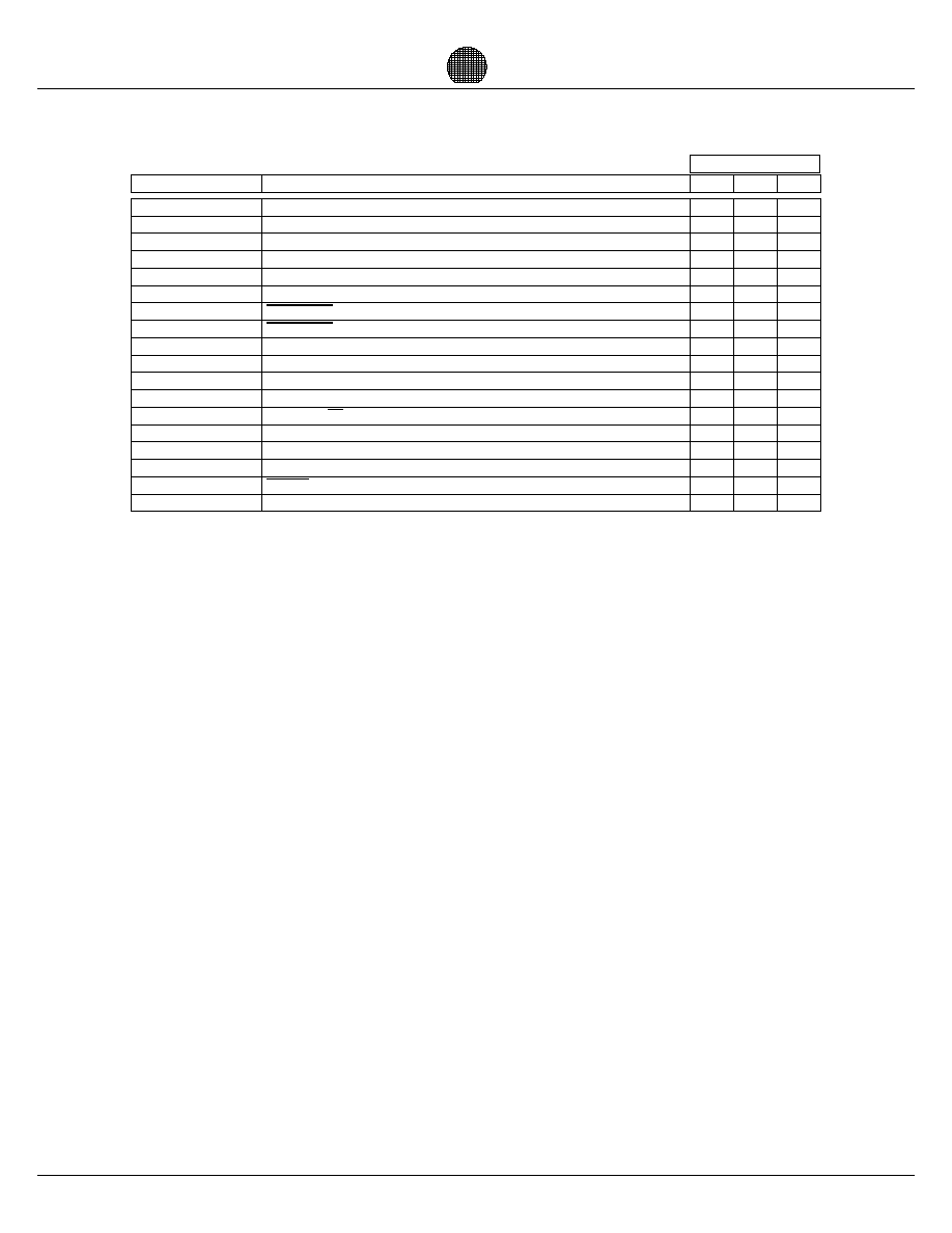
Data Sheet
Page 30
DSP24
Digital Signal Processor
SSCH
HSCH
SGO
HGO
STC
HTC
HZADDR
LZADDR
ODADDR
SSDB
HSDB
ODMRESET
ODRW
ODA0
ODSTART
ODCS
ODBUSY
ODSSYNC
SCHSEL Setup Time (SYSCLK)
SCHSEL Hold Time (SYSCLK)
GO[1:0] Setup Time (SYSCLK)
GO[1:0] Hold Time (SYSCLK)
MMU_TC_A, _B, _C, _D, _E Setup Time (SYSCLK)
MMU_TC_A, _B, _C, _D, _E Hold Time (SYSCLK)
ADDREN High to ADDR[15:0] High-Z
ADDREN Low to ADDR[15:0] Low-Z
ADDR[15:0] Output Valid Delay Time (SYSCLK)
SCHDB[7:0] Setup Time (SYSCLK)
SCHDB[7:0] Hold Time (SYSCLK)
MMU_RESET Output Delay Time (SYSCLK)
MMU_R/W Output Delay Time (SYSCLK)
MMU_A0 Output Delay Time (SYSCLK)
MMU_START Output Delay Time (SYSCLK)
MMU_CS_A, B, C, D, E Output Delay Time (SYSCLK)
BUSY Output Delay Time (SYSCLK)
SSYNC[1:0] Output Delay Time (SYSCLK)
t
t
t
t
t
t
t
t
t
t
t
t
t
t
t
t
t
t
9
9
8
8
8
8
8
8
8
8
8
7
0
6
0
7
0
7
0
AC ELECTRICAL CHARACTERISTICS
SIGNAL
DESCRIPTION
MIN TYP MAX
60 MHz
Note: All clocks signals (CLKxIN, SYSCLK) must be driven, or grounded if not used
DSP
Architectures
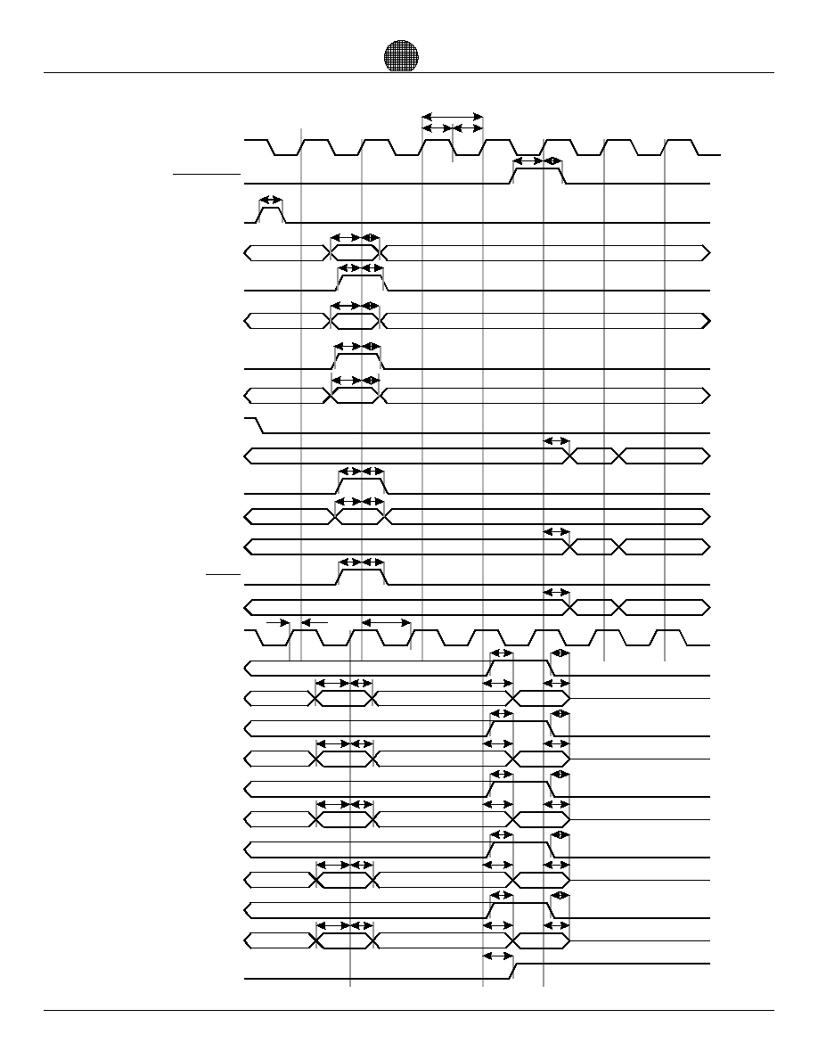
Data Sheet
Page 31
SYSCLK
START/STOP
XSFISEL, XSFI[3:0]
YSFI[3:0], BFPI[5:0]
XCR, XCI
DOCR, DOCI
ENB
BFPCLR
POUT[2:0]
AOE
BOE
COE
DOE
EOE
ERROR
AR[23:0]
AI[23:0]
BR[23:0]
BI[23:0]
CR[23:0]
CI[23:0]
DR[23:0]
DI[23:0]
ER[23:0]
EI[23:0]
SYNCIN[1:0]
SCHSEL
SYNCOUT[1:0]
CLKAIN, CLKBIN
CLKCIN, CLKDIN
CLKEIN
SYSCLKEN
ENA
XZI, YZI, DZO
YCR, YCI, YSWAP
XSWAP
BFPO[[5:0]
DSFO[3:0]
t
SSTART
t
SSYNC
t
SBFPC
t
HSTART
t
HSYNC
t
HBFPC
t
CYC
t
CH
t
CL
t
SKL
t
DSA
t
DODA
t
DODB
t
DODC
t
DODD
t
DODE
t
DODERR
t
DSB
t
DSC
t
DSD
t
DSE
t
DHA
t
DOHA
t
DODSYNC
t
DODCTL
t
DODPOUT
t
LZOEA
t
LZOEB
t
LZOEC
t
LZOED
t
LZOEE
t
HZOEA
t
HZOEB
t
HZOEC
t
HZOED
t
HZOEE
t
DOHB
t
DOHC
t
DOHD
t
DOHE
t
DHB
t
DHC
t
DHD
t
DHE
t
SKT
FC[5:0]
DF[8:0]
RESET
t
RESET
t
SCTLA
t
SCLKEN
t
SCTLB
t
SA
t
SB
t
SCTLC
t
HCTLA
t
HCLKEN
t
HCTLB
t
HA
t
HB
t
HCTLC
Digital Signal Processor
DSP24
DSP
Architectures
AC ELECTRICAL CHARACTERISTICS
Figure 13. DSP24 Timing
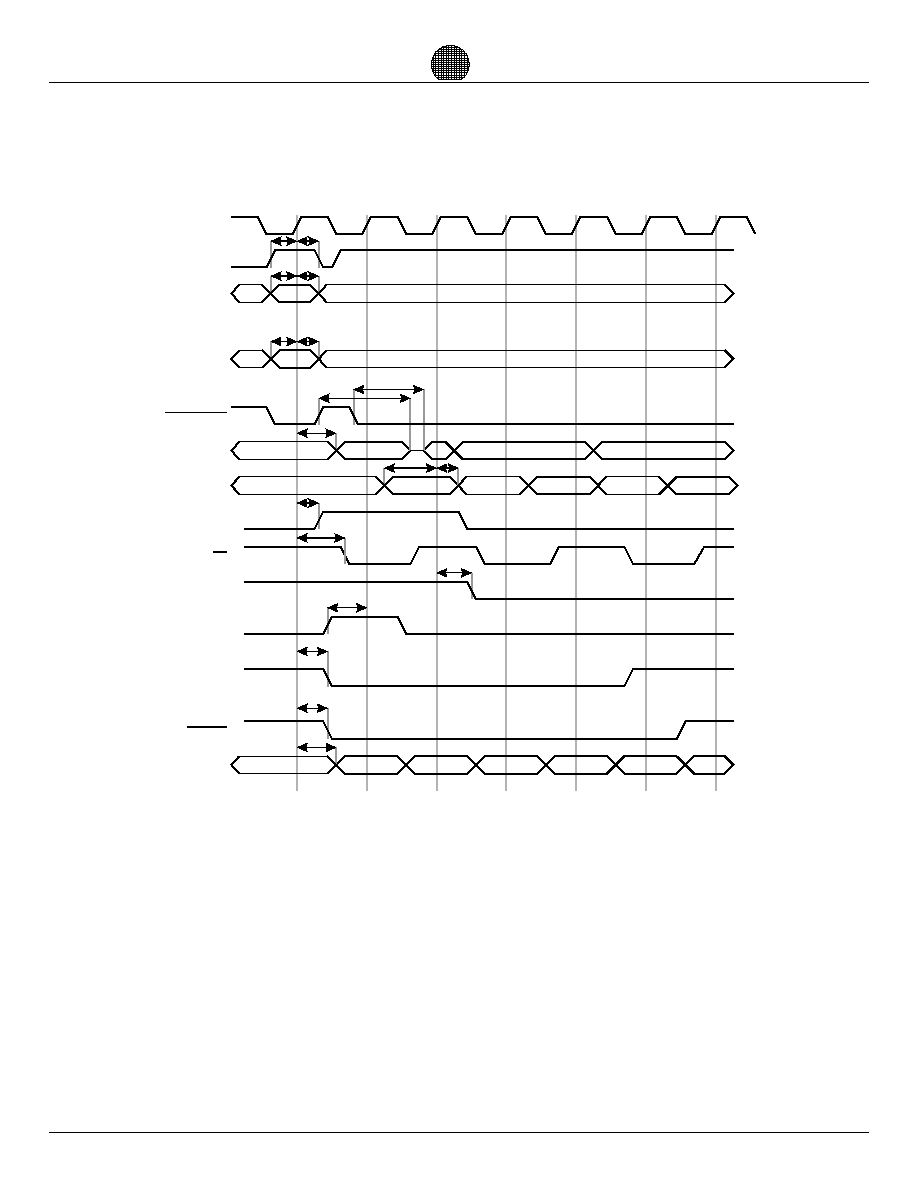
Data Sheet
Page 32
t
ODMRESET
SYSCLK
SCHSEL
GO[1:0]
ADDREN
ADDR[15:0]
MMU_RESET
MMU_R/W
MMU_A0
MMU_START
BUSY
SSYNC[1:0]
MMU_CS_A
MMU_CS_B
MMU_CS_C
MMU_CS_D
MMU_CS_E
SCHDB[7:0]
MMU_TC_A
MMU_TC_B
MMU_TC_C
MMU_TC_D
MMU_TC_E
t
SSCH
t
LZADDR
t
HSDB
t
HZADDR
t
SSDB
t
ODADDR
t
ODRW
t
ODA0
t
ODSTART
t
ODCS
t
ODBUSY
t
ODSSYNC
t
SGO
t
STC
t
HSCH
t
HGO
t
HTC
DSP24
Digital Signal Processor
DSP
Architectures
AC ELECTRICAL CHARACTERISTICS
Figure 13. DSP24 Timing (Continued)
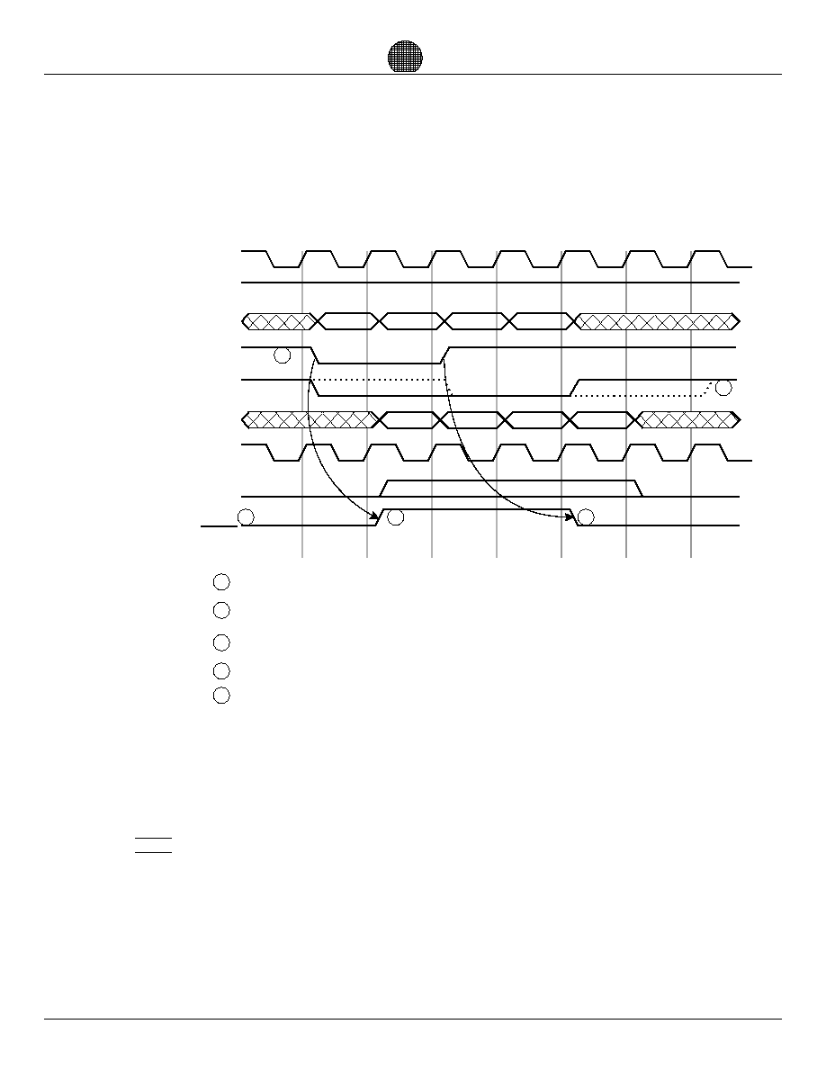
SYSCLK
CLKxIN
INTERNAL TO DSP24
START/STOP
PIA/PIB
ADDR[19:0]
MEMORY DATA
Default TC. (SKEW Reg TC Bits 11:9 = 0, MODE Bit 3 = 0)
The TCx used for START/STOP generation is defined by MSB Bits 8:6 of the programed DataFlow.
The Internal START/STOP rising edge equals Input TC falling edge delayed one clock cycle.
The Internal START/STOP falling edge equals Input TC rising edge delayed two clock cycles.
Default Showed. Depending on memory type, these signals may need to be skewed.
(SKEW Reg Bits 5:3 move MEMW and Bits 2:0 move MEMOE. 7= -1, 0-6 = 0-6)
SCHSEL
2
4
3
5
2
4
5
1
1
3
TCA,TCB,TCC,TCD,TCE
MEMOE/MEMWR
A0
D0
A1
D1
A2
D2
A3
D3
Figure 14. DSP24 Scheduler Mode Timing Diagram
MMU24 to Memory to DSP-24 - Address to Data memory
Latency = 1
Internal to DSP-24 the generated START/STOP signal needs to line up with incoming data first
point, and go low during the incoming data's last point.
System Timing in the Scheduler Mode
When using the DSP24's built in Scheduler, the control for specifying the DSP24's function, data flow, and
various control signals remains the same. However, the source for the contro lsignals has been internally
switched to the output of the internal Scheduler.
START/STOP is the most important of these control signals. As shown in Figures14 and15, the internal
START/STOP is generated from the TC inputs to the Scheduler.
Since latency of the user SRAM is unknown, a value of 1is used for generating the internal timing, see Figure
14.If another type of external SRAM is used, that has a different latency, then the MMU24 must be
programmed to delay its TC output accordingly, see Figure 15.
DSP24
Digital Signal Processor
DSP
Architectures
AC ELECTRICAL CHARACTERISTICS
Data Sheet
Page 33
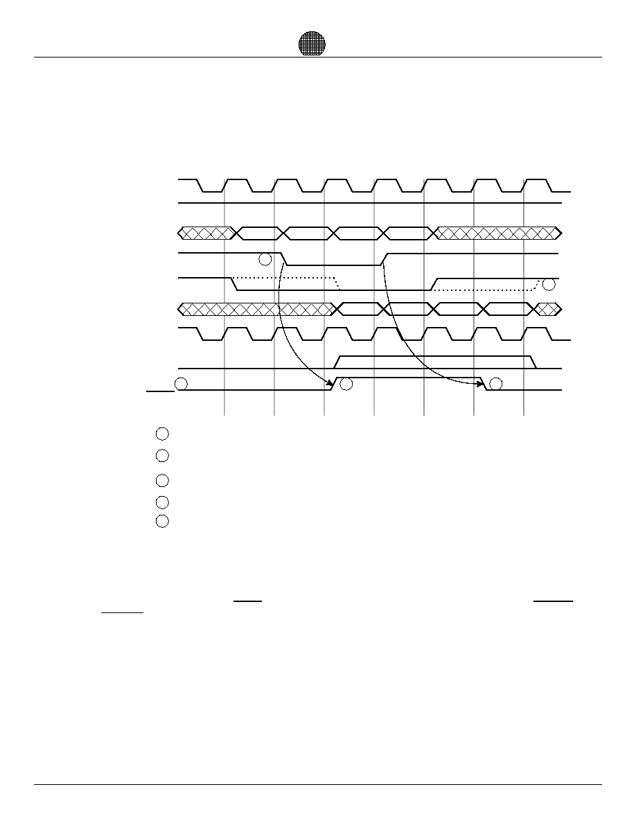
SYSCLK
CLKxIN
INTERNAL TO DSP24
START/STOP
PIA/PIB
ADDR[19:0]
MEMORY DATA
TC delayed by one cycle. (SKEW Reg TC Bits 11:9 = 1, MODE Bit 3 = 0)
The TCx used for START/STOP generation is defined by MSB Bits 8:6 of the programed DataFlow.
Internal to DSP-24 the generated START/STOP signal needs to line up with incoming data first
point, and go low during the incoming data's last point.
The Internal START/STOP rising edge equals Input TC falling edge delayed one clock cycle.
The Internal START/STOP falling edge equals Input TC rising edge delayed two clock cycles.
Default Showed. Depending on memory type, these signals may need to be skewed.
(SKEW Reg Bits 5:3 move MEMW and Bits 2:0 move MEMOE. 7= -1, 0-6 = 0-6)
SCHSEL
2
4
3
5
2
4
5
1
1
3
TCA,TCB,TCC,TCD,TCE
MEMOE/MEMWR
A0
D0
A1
D1
A2
D2
A3
D3
MMU24 to Memory to DSP-24 - Address to Data memory
Latency = 2
System Timing in the Scheduler Mode (Continued)
In addition to setting the START/ STOP timing, the MMU24 must also be programmed to skew the MEMOE
and MEMWR signals to the SRAM. This frames the active data, according to the SRAM's specification.
DSP24
Digital Signal Processor
DSP
Architectures
AC ELECTRICAL CHARACTERISTICS
Data Sheet
Page 34
Figure 15. DSP24 Scheduler Mode Timing Diagram (Continued)

Data Sheet
Page 35
Digital Signal Processor
DSP24
SBGA PHYSICAL DEMINSIONS
DSP
Architectures
BGA Package - BGA432
BGA Package - BGA432
Data Sheet
Page 36
DSP24
Digital Signal Processor
PIN LIST:
DSP
Architectures
C18
B28
D27
B27
A27
D26
C27
A28
A26
C25
B26
C26
D23
B25
A25
C24
D24
A23
B23
C23
A24
B24
C21
D21
B22
A22
C22
B20
A21
C20
D19
D20
B21
B19
A19
A20
C19
B18
D17
POUT0
PIA ENA
POUT1
JCK
JMS
JDI
XSFI1
XSFI0
BFPI5
BFPI4
BFPI3
BFPI2
BFPI1
BFPI0
JDO
GO1
GO0
SYNCIN1
SYNCIN0
RESET
JRST
POUT2
N/C
N/C
N/C
BUSY
ALG7 DOCI
ALG6 DOCR
ALG5 XCR
ALG4 YSFI3
ALG3 YSFI2
ALG2 YSFI1
ALG1 YSFI0
ALG0 XSFISEL
ADDR15 FC0
ADDR14 FC1
ADDR13 FC2
ADDR12 FC3
PIB ENB
C16
A16
C17
B16
B15
C15
B14
D16
A15
B13
D15
C14
A13
AI10
AI09
AI08
AI07
AI06
AI05
AI04
AI03
AI02
AI01
AI00
XSFI3
XSFI2
B11
C13
A11
C12
A12
B12
D13
A8
D11
B10
C11
D12
A10
C9
A9
B9
C10
A7
B7
B8
D9
C8
B6
C7
A6
D8
CLKAIN
AI23
AI22
AI21
AI20
AI19
AI18
AI17
AI16
AI15
AI14
AI13
AI12
AR11
AI11
AR10
AR09
AR08
AR07
AR06
AR05
AR04
AR03
AR02
AR01
AR00
C5
B5
A5
C6
D6
B4
A4
D5
AR19
AR18
AR17
AR16
AR15
AR14
AR13
AR12
L3
M4
L2
L1
M3
N4
J2
J1
K3
L4
K2
K1
G1
J4
J3
G2
H3
H2
H1
F3
F2
F1
G3
H4
D2
D1
E3
F4
E2
E1
E4
AR23
AR22
AR21
AR20
CLKBIN
BI23
BI22
BI21
BI20
BI19
BI18
BI17
BI16
BI15
BI14
BI13
BI12
BI11
BI10
BI09
BI08
BI07
BI06
BI05
BI04
BI03
BI02
BI01
BI00
MMUCSA
AOE
M1
N3
M2
BR02
BR01
BR00
AC2
AC3
AD1
AD2
Y4
AA3
AB1
AB2
AA4
AB3
AC1
W3
Y1
Y2
W4
Y3
AA1
AA2
U2
U3
V2
U4
V3
W1
W2
R4
R3
T1
T2
T3
T4
U1
N2
N1
P3
P2
BR23
BR22
BR21
BR20
BR19
BR18
BR17
BR16
BR15
BR14
BR13
BR12
BR11
BR10
BR09
BR08
BR07
BR06
BR05
BR04
BR03
CI12
CI11
CI10
CI09
CI08
CI07
CI06
CI05
CI04
CI03
CI02
CI01
CI00
BOE
MMUCSB
Data Sheet
Page 37
PIN LIST (cont):
Digital Signal Processor
DSP24
DSP
Architectures
AH1
AH2
AG4
AF3
AG1
AG2
AF4
AG3
AD3
AE1
AE2
AD4
AE3
AF1
AF2
AC4
CI23
CI22
CI21
CI20
CI19
CI18
CI17
CI16
CI15
CI14
CI13
CLKCIN
CR03
CR02
CR01
CR00
AL8
AH11
AK9
AJ10
AJ9
AJ8
AH9
AK8
AK7
AL7
AL6
AJ7
AH8
AK6
AK5
AL5
AJ6
AJ5
AH6
AK4
AL4
AH5
AL9
CR23
CR22
CR21
CR20
CR19
CR18
CR17
CR16
CR15
CR14
CR13
CR12
CR11
CR10
CR09
CR08
CR07
CR06
CR05
CR04
MMUCSC
COE
DSFO3
AJ18
AJ21
AL22
AK20
AL21
AH20
AK21
AJ20
AH19
AL20
AJ19
AK19
AL19
AK11
AH16
AJ17
AH17
AK18
AK17
AL17
AL16
AJ16
AK16
AJ15
AH15
AJ14
AK14
AL13
AK13
AJ13
AH13
AK12
AL12
AL11
AJ12
AL10
AJ11
AH12
AK10
DR02
DR01
DR00
DI23
DI22
DI21
DI20
DI19
DI18
DI17
DI16
DI15
DI14
DI13
DI12
DI11
DI10
DI09
DI08
DI07
DI06
DI05
DI04
DI03
DI02
DI01
DI00
CLKDIN
DSFO2
DSFO1
DSFO0
BFPO5
BFPO4
BFPO3
BFPO2
BFPO1
BFPO0
SYNCOUT0
SYNCOUT1
AK28
AH27
AH26
AJ27
AL28
AK27
AL27
AK26
AJ26
AJ25
AL26
AL25
AK25
AH24
AH23
AJ24
AL23
AJ23
AL24
AK24
AK23
AK22
AH21
AJ22
DR23
DR22
DR21
DR20
DR19
DR18
DR17
DR16
DR15
DR14
DR13
DR12
DR11
DR10
DR09
DR08
DR07
DR06
DR05
DR04
DR03
EI00
DOE
MMUCSD
AG28
AH30
AH31
AG30
AG31
AF29
AG29
AF28
AD29
AD28
AE30
AE31
AF30
AF31
AE29
EI15
EI14
EI13
EI12
EI11
EI10
EI09
EI08
EI07
EI06
EI05
EI04
EI03
EI02
EI01
AC29
AC30
AC28
AD30
AD31
AA29
Y28
AC31
AB29
AA28
AB30
AB31
Y31
W29
AA30
AA31
Y29
W28
Y30
T31
U29
W30
W31
V29
V30
U28
P30
T30
T29
T28
R31
R30
R29
R28
P29
N31
N30
N29
M31
EI23
EI22
EI21
EI20
EI19
EI18
EI17
EI16
CLKEIN
ER23
ER22
ER21
ER20
ER19
ER18
ER17
ER16
ER15
ER14
ER13
ER12
ER11
ER10
ER09
ER08
ER07
ER06
ER05
ER04
ER03
ER02
ER01
ER00
EOE
MMUCSE
START/STOP
SYSCLKEN
SYSCLK
YCR
Data Sheet
Page 38
DSP24
Digital Signal Processor
DSP
Architectures
M30
N28
M29
L31
L30
M28
L29
K31
K30
L28
K29
J31
J30
H31
H30
J28
H29
G31
G30
J29
G29
F31
F30
F29
H28
E30
F28
E29
D31
D30
E31
E28
ADDR11 FC4
ADDR10 FC5
ADDR9 BFPCLR
ADDR8 DF8
ADDR7 DF7
ADDR6 DF6
ADDR5 DF5
ADDR4 DF4
ADDR3 DF3
ADDR2 DF2
ADDR1 DF1
ADDR0 DF0
ADDREN
MMU_START
MMU_A0
MMU_R/W
SCH_DB7
SCH_DB6
SCH_DB5
SCH_DB4
SCH_DB3
SCH_DB2
SCH_DB1
SCH_DB0
MMUTCE DZO
MMUTCD YZI
MMUTCC XZI
MMUTCB XCI
MMUTCA XSWAP
SCHSEL
YCI
YSWAP
PIN LIST (cont):
Data Sheet
Page 39
Digital Signal Processor
DSP24
DSP
Architectures
A1
V4
A31
V28
B2
AB4
B30
AE4
C3
AB28
C29
AE28
D4
AH4
D7
AH7
D10
AH10
D14
AH14
D18
AH18
D22
AH22
D25
AH25
D28
AH28
G4
AJ3
G28
AJ29
K4
AK2
K28
AK30
P4
AL1
P28
AL31
A2
U30
A3
U31
A14
V1
A17
V31
A18
AH3
A29
AH29
A30
AJ1
B1
AJ2
B3
AJ4
B17
AJ30
B29
AJ28
B31
AJ31
C1
AK1
C2
AK3
C4
AK15
C28
AK29
C30
AK31
C31
AL2
D3
AL3
D29
AL14
P1
AL15
P31
AL18
R1
AL29
R2
AL30
VCC:
GND:
PIN LIST (cont):
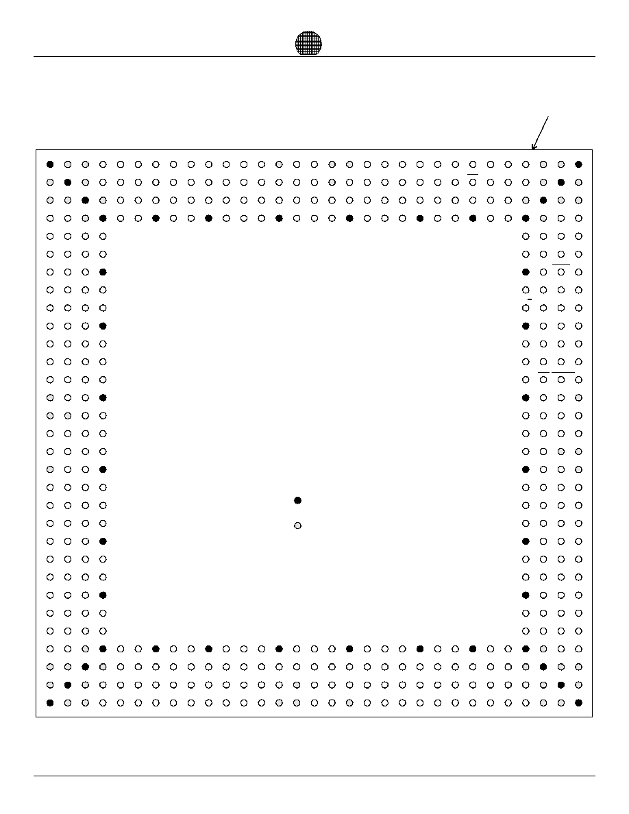
Data Sheet
Page 40
MMU-24
Digital Signal Processor
DSP
Architectures
PACKAGE DRAWING: 432-PIN SBGA PIN CONNECTIONS
TOP
VIEW
1
1
2
2
3
3
4
4
5
5
6
6
7
7
8
8
9
9
10
10
11
11
12
12
13
13
14
14
15
15
16
16
17
17
18
18
19
19
20
20
21
21
22
22
27
27
23
23
28
28
24
24
29
29
25
25
30
30
26
26
31
31
AL
AL
AK
AK
AJ
AJ
AH
AH
AG
AG
AF
AF
AE
AE
AD
AD
AC
AC
AB
AB
AA
AA
Y
Y
W
W
V
V
U
U
T
T
R
R
P
P
N
N
M
M
L
L
K
K
J
J
H
H
G
G
F
F
E
E
D
D
C
C
B
B
A
A
AR23
AR22
AR21
AR20
CLKBIN
BR23
BI23
BR22
BI22
BR21
BI21
BR20
BI20
BR19
BI19
BR18
BI18
BR17
BI17
BR16
BI16
BR15
BI15
BR14
BI14
BR13
BI13
BR12
BI12
BR11
BI11
BR10
BI10
BR09
BI09
BR08
BI08
BR07
BI07
BR06
BI06
BR05
BI05
BR04
BI04
BR03
BI03
BR02
BI02
BR01
BR00
BI01
BI00
CI23
CI22
CI21
CI20
CI19
CI18
CI17
CI16
CI15
CI14
CI13
CI12
CI11
CI10
CI09
CI08
CI07
CI06
CI05
CI04
CI03
CI02
CI01
CI00
CLKCIN
CR03
CR02
CR01
CR00
MMUCSA
AOE
BOE
MMUCSB
EI23
EI22
EI21
EI20
EI19
EI18
EI17
EI16
EI15
EI14
EI13
EI12
EI11
EI10
EI09
EI08
EI07
EI06
EI05
EI04
EI03
EI02
EI01
CLKEIN
ER23
ER22
ER21
ER20
ER19
ER18
ER17
ER16
ER15
ER14
ER13
ER12
ER11
ER10
ER09
ER08
ER07
ER06
ER05
ER04
ER03
ER02
ER01
ER00
EOE
MMUCSE
START/
STOP SYSCLKEN SYSCLK
ADDR11
FC4
ADDR10
FC5
ADDR9
BFPCLR
ADDR8
DF8
ADDR7
DF7
ADDR6
DF6
ADDR5
DF5
ADDR4
DF4
ADDR3
DF3
ADDR2
DF2
ADDR1
DF1
ADDR0
DF0
ADDREN MMU_START
MMU_A0
MMU_R/W
SCH_DB7 SCH_DB6
SCH_DB5 SCH_DB4 SCH_DB3
SCH_DB2
SCH_DB1
SCH_DB0
MMUTCE
DZO
MMUTCD
YZI
MMUTCC
XZI
MMUTCB
XCI
MMUTCA
XSWAP
SCHSEL
YCR
YCI
YSWAP
CLKAIN
AI23
AI22
AI21
AI20
AR19
AI19
AR18
AI18
AR17
AI17
AR16
AI16
AR15
AI15
AR14
AI14
AR13
AI13
AR12
AI12
AR11
AI11
AR10
AI10
AR09
AI09
AR08
AI08
AR07
AI07
AR06
AI06
AR05
AI05
AR04
AI04
AR03
AI03
AR02
AI02
AR01
AI01
AR00
AI00
POUT0
PIA
ENA
POUT1
JCK
JMS
JDI
XSFI3
XSFI2
XSFI1
XSFI0
BFPI5
BFPI4
BFPI3
BFPI2
BFPI1
BFPI0
JDO
GO1
GO0
SYNCIN1
SYNCIN0
RESET
JRST
POUT2
N/C
N/C
N/C
BUSY
ALG7
DOCI
ALG6
DOCR
ALG5
XCR
ALG4
YSFI3
ALG3
YSFI2
ALG2
YSFI1
ALG1
YSFI0
ALG0
XSFISEL
ADDR15
FC0
ADDR14
FC1
ADDR13
FC2
ADDR12
FC3
PIB
ENB
CR23
CR22
CR21
CR20
CR19
CR18
CR17
CR16
CR15
CR14
CR13
CR12
CR11
CR10
CR09
CR08
CR07
CR06
CR05
CR04
DR23
DR22
DR21
DR20
DR19
DR18
DR17
DR16
DR15
DR14
DR13
DR12
DR11
DR10
DR09
DR08
DR07
DR06
DR05
DR04
DR03
DR02
DR01
DR00
DI23
DI22
DI21
DI20
DI19
DI18
DI17
DI16
DI15
DI14
DI13
DI12
DI11
DI10
DI09
DI08
DI07
DI06
DI05
DI04
DI03
DI02
DI01
DI00
CLKDIN
EI00
MMUCSC
COE
DSFO3
DSFO2
DSFO1
DSFO0
BFPO5
BFPO4
BFPO3
BFPO2
BFPO1
BFPO0
DOE
MMUCSD
SYNCOUT0
SYNCOUT1
=Vcc
=Gnd
SBGA432
note: top label is with SCHSEL=1
i.e. A28=ADDR14 when SCHSEL=1
and A28=FC1 when SCHSEL=0
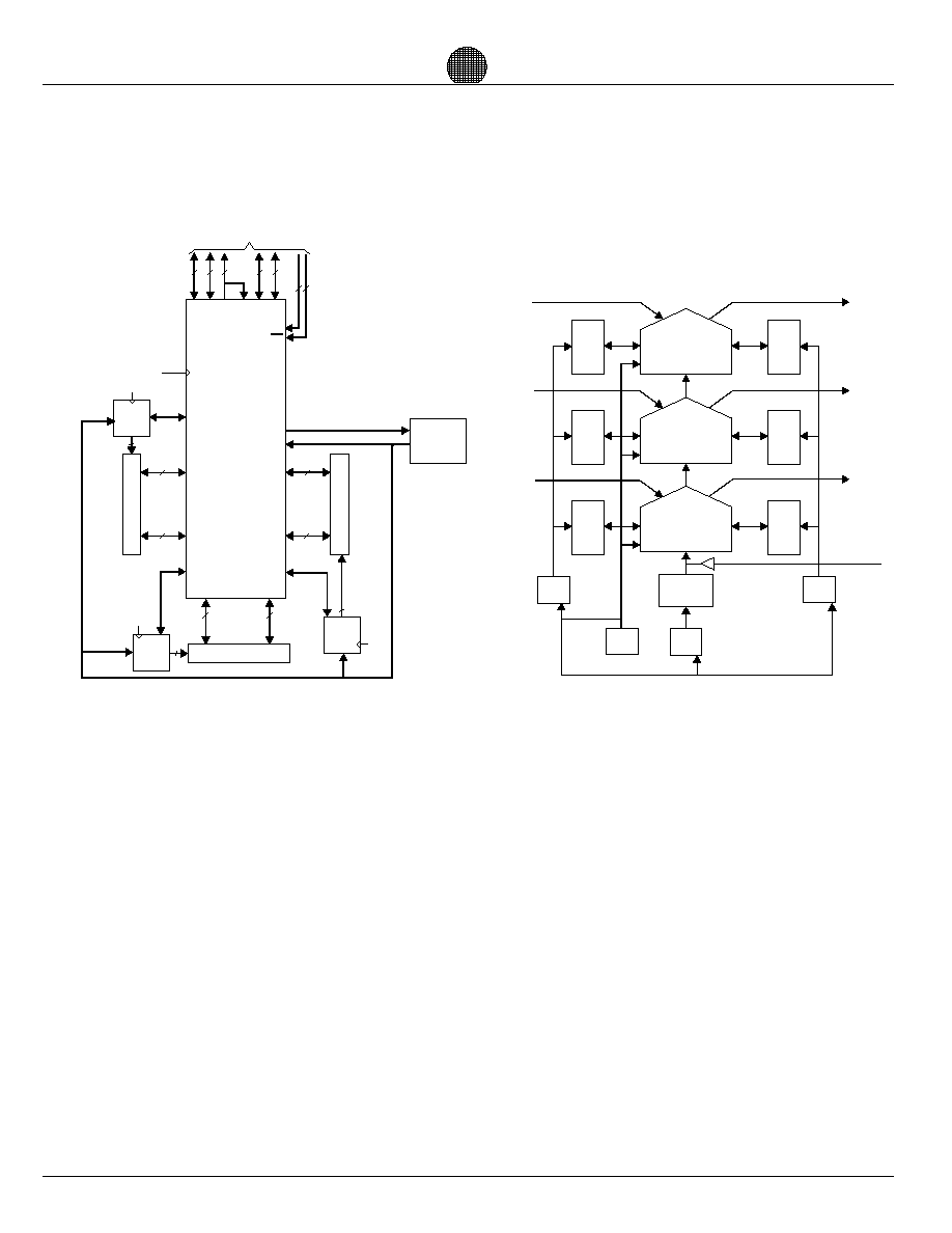
Data Sheet
Page 41
Digital Signal Processor
DSP24
MMU-24
MMU-24
MMU-24
DSP24
S
R
A
M
SRAM
S
R
A
M
Ar
Dr
Er
Di
Ei
Br
Bi
Ai
Cr
Ci
Control
DB[7:0]
ADDR[15:0]
Control
Control
24
24
24
24
4
ALG
GO
8
2
24
24
24
15
15
15
24
24
24
SYSTEM
CLOCK
SYSTEM
CLOCK
SYSTEM
CLOCK
SYSTEM
CLOCK
B
F
P
O
B
F
P
I
USER INTERFACE
TYPICAL RECURSIVE SYSTEM:
TYPICAL PARALLEL SYSTEM:
CONTROL
PROM
The user supplied CONTROL PROM supplies
the following:
"
INPUT ZERO FILLING
"
OUTPUT ZERO FILLING
"
INPUT ZERO PADDING
"
OUTPUT ZERO PADDING
"
INPUT DATA SHIFTING
"
INPUT DATA COMPLEMENTING
"
INITIALIZATION PROGRAMMING FOR UP TO
FIVE MMU-24's
"
ADDRESS PATTERNS FOR EACH ONE OF
UP TO FIVE MMU-
24's
"
SYSTEM START/STOP MANAGEMENT
"
SYSTEM SYNCHRONIZATION
RAM
RAM
RAM
RAM
RAM
RAM
RAM
MMU
-24
prom
MMU
-24
MMU
-24
Channel
0 to 49
Channel
0 to 49
Channel
50 to 99
Channel
50 to 99
Channel
100 to 149
Channel
100 to 149
Adaptive Filter
Updates
DSP24
A
B
C
D
E
DSP24
A
B
C
D
E
DSP24
A
B
C
D
E
DSP
Architectures
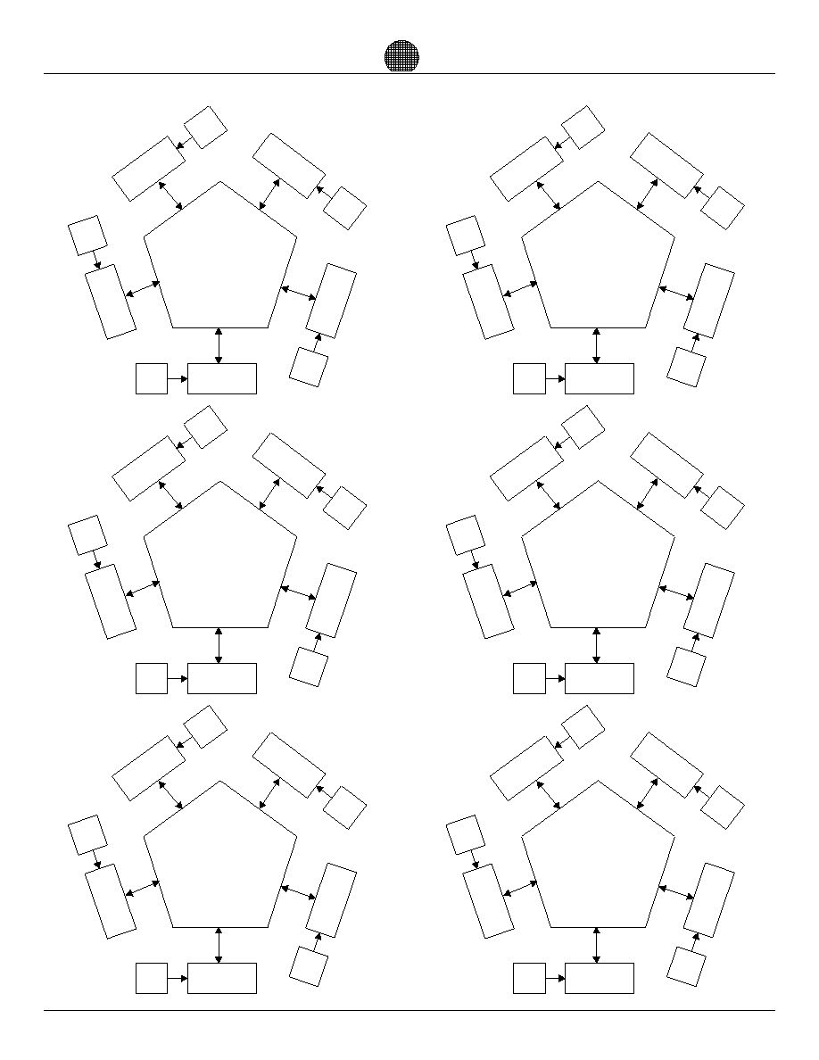
Data Sheet
Page 42
DSP24
Digital Signal Processor
DATA FLOW WORKSHEET
M
M
U
M
M
U
M
M
U
MU
M
SS
A
M
R
A
SS
R
M
SS
R
A
M
SRA
S
M
DSP24
MMU
SSRAM
A
B
C
D
E
M
M
U
M
M
U
M
U
M
MU
M
SS
A
R
M
SR
AM
S
SS
R
A
M
SSR
AM
DSP24
MMU
SSRAM
A
B
C
D
E
M
M
U
M
M
U
M
M
U
MU
M
SS
A
M
R
A
SS
R
M
SS
R
A
M
SSR
AM
DSP24
MMU
SSRAM
A
B
C
D
E
M
M
U
M
M
U
M
M
U
MU
M
SS
A
R
M
SR
AM
S
SS
R
A
M
SSR
AM
DSP24
MMU
SSRAM
A
B
C
D
E
M
M
U
M
M
U
M
U
M
MU
M
SS
A
R
M
A
SS
R
M
SS
R
A
M
SSR
AM
DSP24
MMU
SSRAM
A
B
C
D
E
M
M
U
M
M
U
M
M
U
MU
M
SS
A
R
M
SS
RA
M
SS
A
R
M
SSR
AM
DSP24
MMU
SSRAM
A
B
C
D
E
DSP
Architectures

Data Sheet
Page 43
Digital Signal Processor
DSP24
DSP
Architectures
Notes:

DSP24
Digital Signal Processor
ORDERING INFORMATION
Speed
Package
Temperature
Device
20, 40, 60, 80, 100 Operating Frequency (MHz)
#
#
#
#
Example: DSP24-Y-100-C (432-Lead BGA, 100 MHz Operating Frequency, Commercial Temperature)
DSP24
-
-
-
Y = 432-lead BGA
DSP Architectures Inc. reserves the right to make changes in specifications at any time without notice. DSP Architectures Inc.
does not assume any responsibility for the use of any circuitry described; no circuit patent licenses are implied.
NORTH AMERICA
Digital Signal Processing Architectures Inc.
7902 NE St. Johns Rd. Bldg 102
Vancouver, WA 98665, USA
Phone: 360 573-4084
Fax: 360 573-4272
Web Page: www.dsparchitectures.com
Reference DSPA-DSP24DS
DSP Architectures Inc. 2002 Printed and bound in the USA.
M=Military, I=Industrial, C=Commercial
DSP
Architectures
Architectures
TM
Transform Your World
DSP