
Other brands and names are the property of their respective owners
Information in this document is provided in connection with Intel products Intel assumes no liability whatsoever including infringement of any patent or
copyright for sale and use of Intel products except as provided in Intel's Terms and Conditions of Sale for such products Intel retains the right to make
changes to these specifications at any time without notice Microcomputer Products may have minor variations to this specification known as errata
December 1995
COPYRIGHT
INTEL CORPORATION 1995
Order Number 290449-006
2-MBIT (128K x 16 256K x 8)
LOW-POWER BOOT BLOCK
FLASH MEMORY FAMILY
28F200BL-T B 28F002BL-T B
Y
Low Voltage Operation for Very Low
Power Portable Applications
V
CC
e
3 0V ≠ 3 6V
Y
Expanded Temperature Range
b
20 C to
a
70 C
Y
x8 x16 Input Output Architecture
28F200BL-T 28F200BL-B
For High Performance and High
Integration 16-bit and 32-bit CPUs
Y
x8-only Input Output Architecture
28F002BL-T 28F002BL-B
For Space Constrained 8-bit
Applications
Y
Upgradeable to Intel's SmartVoltage
Products
Y
Optimized High-Density Blocked
Architecture
One 16-KB Protected Boot Block
Two 8-KB Parameter Blocks
One 96-KB Main Block
One 128-KB Main Block
Top or Bottom Boot Locations
Y
Extended Cycling Capability
10 000 Block Erase Cycles
Y
Automated Word Byte Write and Block
Erase
Command User Interface
Status Registers
Erase Suspend Capability
Y
SRAM-Compatible Write Interface
Y
Automatic Power Savings Feature
0 8 mA Typical I
CC
Active Current in
Static Operation
Y
Very High-Performance Read
150 ns Maximum Access Time
65 ns Maximum Output Enable Time
Y
Low Power Consumption
15 mA Typical Active Read Current
Y
Reset Deep Power-Down Input
0 2 mA I
CC
Typical
Acts as Reset for Boot Operations
Y
Write Protection for Boot Block
Y
Hardware Data Protection Feature
Erase Write Lockout during Power
Transitions
Y
Industry Standard Surface Mount
Packaging
28F200BL JEDEC ROM Compatible
44-Lead PSOP
56-Lead TSOP
28F002BL 40-Lead TSOP
Y
12V Word Byte Write and Block Erase
V
PP
e
12V
g
5% Standard
Y
ETOX
TM
III Flash Technology
3 3V Read
Y
Independent Software Vendor Support

28F200BL-T B 28F002BL-T B
Intel's 2-Mbit Low Power Flash Memory Family is an extension of the Boot Block Architecture which includes
block-selective erasure automated write and erase operations and standard microprocessor interface The
2-Mbit Flash Memory Family enhances the Boot Block Architecture by adding more density and blocks
x8 x16 input output control very low power very high speed an industry standard ROM compatible pinout
and surface mount packaging The 2-Mbit Low Power Flash Family opens a new capability for 3V battery-oper-
ated portable systems and allows for an easy upgrade to Intel's 4-Mbit Low Power Boot Block Flash Memory
Family
The Intel 28F200BL-T B are 16-bit wide flash memory offerings These high density flash memories provide
user selectable bus operation for either 8-bit or 16-bit applications The 28F200BL-T and 28F200BL-B are
2 097 152-bit non-volatile memories organized as either 262 144 bytes or 131 072 words of information They
are offered in 44-Lead plastic SOP and 56-Lead TSOP packages The x8 x16 pinout conforms to the industry
standard ROM EPROM pinout
The Intel 28F002BL-T B are 8-bit wide flash memories with 2 097 152 bits organized as 262 144 bytes of
information They are offered in a 40-Lead TSOP package which is ideal for space-constrained portable
systems
These devices use an integrated Command User Interface (CUI) and Write State Machine (WSM) for simplified
word byte write and block erasure The 28F200BL-T 28F002BL-T provide block locations compatible with
Intel's low voltage MCS-186 family i386
TM
i486
TM
microprocessors The 28F200BL-B 28F002BL-B provide
compatibility with Intel's 80960KX and 80960SX families as well as other low voltage embedded microproces-
sors
The boot block includes a data protection feature to protect the boot code in critical applications With a
maximum access time of 150 ns these 2-Mbit flash devices are very high performance low power memories
which interface to a wide range of low power microprocessors and microcontrollers A deep power-down mode
lowers the total V
CC
power consumption to 0 66 mW This is critical in handheld battery powered systems such
as Handy Phones For very high speed applications using a 5V supply refer to the Intel 28F200BX-T B
28F002BX-T B 2-Mbit Boot Block Flash Memory Family datasheet
Manufactured on Intel's 0 8 micron ETOX III process the 2-Mbit low power flash memory family provides world
class quality reliability and cost-effectiveness at the 2-Mbit density level
2
28F200BL-T B 28F002BL-T B
1 0
PRODUCT FAMILY OVERVIEW
Throughout this datasheet 28F200BL refers to both
the 28F200BL-T and 28F200BL-B devices and
28F002BL refers to both the 28F002BL-T and
28F002BL-B devices The 2-Mbit flash family refers
to both the 28F200BL and 28F002BL products This
datasheet comprises the specifications for four sep-
arate products in the 2-Mbit flash memory family
Section 1 provides an overview of the 2-Mbit flash
memory family including applications pinouts and
pin descriptions Sections 2 and 3 describe in detail
the specific memory organizations for the 28F200BL
and 28F002BL products respectively
Section 4
combines a description of the family's principles of
operations Finally section 5 describes the family's
operating specifications
PRODUCT FAMILY
x8 x16 Products
x8-Only Products
28F200BL-T
28F002BL-T
28F200BL-B
28F002BL-B
1 1 Designing for Upgrade to
SmartVoltage Products
Today's high volume boot block products are up-
gradable to Intel's SmartVoltage boot block prod-
ucts that provide program and erase operation at 5V
or 12V V
PP
and read operation at 3V or 5V V
CC
Intel's SmartVoltage boot block products provide the
following enhancements to the boot block products
described in this data sheet
1 DU pin is replaced by WP
to provide a means
to lock and unlock the boot block with logic sig-
nals
2 5V Program Erase operation uses proven pro-
gram and erase techniques with 5V
g
10% ap-
plied to V
PP
3 Enhanced circuits optimize performance at 3 3V
V
CC
Refer to the 2 4 or 8 Mbit SmartVoltage Boot Block
Flash Memory Data Sheets for complete specifica-
tions
When you design with 12V V
PP
boot block products
you should provide the capability in your board de-
sign to upgrade to SmartVoltage products
Follow these guidelines to ensure compatibility
1 Connect DU (WP
on SmartVoltage products) to
a control signal or to V
CC
or GND
2 If adding a switch on V
PP
for write protection
switch to GND for complete write protection
3 Allow for connecting 5V to V
PP
and disconnect
12V from line V
PP
line if desired
1 2 Main Features
The 28F200BL 28F002BL low power boot block
flash memory family is a very low power and very
high performance 2-Mbit (2 097 152 bit) memory
family organized as either 128 Kwords (131 072
words) of 16 bits each or 256 Kbytes (262 144
bytes) of 8 bits each
Five Separately Erasable Blocks
including a Hard-
ware-Lockable boot block
(16 384 Bytes) two pa-
rameter blocks
(8 192 Bytes each) and two main
blocks
(1 block of 98 304 Bytes and 1 block of
131 072 Bytes) are included on the 2-Mbit family An
erase operation erases one of the 5 blocks in typi-
cally 3 4 seconds and the boot or parameter blocks
in typically 2 0 seconds independent of the remain-
ing blocks Each block can be independently erased
and programmed 10 000 times
The Boot Block
is located at either the top
(28F200BL-T
28F002BL-T)
or
the
bottom
(28F200BL-B 28F002BL-B) of the address map in
order to accommodate different microprocessor pro-
tocols for boot code location The hardware locka-
ble boot block
provides the most secure code stor-
age The boot block is intended to store the kernel
code required for booting-up a system When the
RP
pin is between 11 4V and 12 6V the boot block
is unlocked and program and erase operations can
be performed When the RP
pin is at or below 4 1V
the boot block is locked and program and erase op-
erations to the boot block are ignored
The 28F200BL products are available in the
ROM EPROM compatible pinout and housed in the
44-Lead PSOP (Plastic Small Outline) package and
the 56-Lead TSOP (Thin Small Outline 1 2 mm
thick) package as shown in Figures 3 and 4 The
28F002BL products are available in the 40-Lead
TSOP (1 2 mm thick) package as shown in Figure 5
The Command User Interface (CUI) serves as the
interface between the microprocessor or microcon-
troller and the internal operation of the 28F200BL
and 28F002BL flash memory products
3

28F200BL-T B 28F002BL-T B
Program and Erase Automation
allow program
and erase operations to be executed using a two-
write command sequence to the CUI The internal
Write State Machine (WSM) automatically executes
the algorithms and timings necessary for program
and erase operations including verifications there-
by unburdening the microprocessor or microcontrol-
ler Writing of memory data is performed in word or
byte increments for the 28F200BL family and in byte
increments for the 28F002BL family typically within
11 ms
The Status Register (SR) indicates the status of the
WSM and whether the WSM successfully completed
the desired program or erase operation
Maximum Access Time of 150 ns (t
ACC
)
is achieved
over the commercial temperature range (0 C to
a
70 C) over V
CC
supply voltage range (3 0V to
3 6V 4 5V to 5 5V) and 50 pF output load
I
PP
Program current is 40 mA for x16 operation
and 30 mA for x8 operation I
PP
Erase current is
30 mA maximum V
PP
erase and programming
voltage is 11 4V to 12 6V (V
PP
e
12V
g
5%) un-
der all operating conditions
Typical I
CC
Active Current of 15 mA
is achieved
for the x16 products and the x8 products
The 2-Mbit flash family is also designed with an Au-
tomatic Power Savings (APS) feature to minimize
system battery current drain and allow for extremely
low power designs Once the device is accessed to
read the array data APS mode will immediately put
the memory in static mode of operation where I
CC
active current is typically 0 8 mA until the next read
is initiated
When the CE
and RP
pins are at V
CC
and the
BYTE
pin (28F200BL-only) is at either V
CC
or GND
the CMOS Standby mode is enabled where I
CC
is
typically 40 mA
A Deep Power-down Mode is enabled when the
RP
pin is at ground minimizing power consumption
and providing write protection during power-up con-
ditions I
CC
current
during deep power-down mode
is 0 20 mA typical An initial maximum access time
or Reset Time of 600 ns is required from RP
switching until outputs are valid Equivalently the
device has a maximum wake-up time of 1 ms until
writes to the Command User Interface are recog-
nized When RP
is at ground the WSM is reset the
Status Register is cleared and the entire device is
protected from being written to This feature pre-
vents data corruption and protects the code stored
in the device during system reset The system Reset
pin can be tied to RP
to reset the memory to nor-
mal read mode upon activation of the Reset pin
When the CPU enters reset mode it expects to read
the contents of a memory location Furthermore
with on-chip program erase automation in the
2-Mbit family and the RP
functionality for data pro-
tection after the CPU is reset and even if a program
or erase command is issued the device will not rec-
ognize any operation until RP
returns to its normal
state
For the 28F200BL Byte-wide or Word-wide In-
put Output Control
is possible by controlling the
BYTE
pin When the BYTE
pin is at a logic low
the device is in the byte-wide mode (x8) and data is
read and written through DQ 0 7
During the byte-
wide mode DQ 8 14 are tri-stated and DQ
15
A
b
1
becomes the lowest order address pin When the
BYTE
pin is at a logic high the device is in the
word-wide mode (x16) and data is read and written
through DQ 0 15
1 3 Applications
The 2-Mbit low power boot block flash memory fami-
ly combines high density 3V operation high per-
formance cost-effective flash memories with block-
ing and hardware protection capabilities Its flexibility
and versatility will reduce costs throughout the prod-
uct life cycle Flash memory is ideal for Just-In-Time
production flow
reducing system inventory and
costs and eliminating component handling during
the production phase During the product life cycle
when code updates or feature enhancements be-
come necessary flash memory will reduce the up-
date costs by allowing either a user-performed code
change via floppy disk or a remote code change via
a serial link The 2-Mbit boot block flash memory
family provides full function blocked flash memories
suitable for a wide range of applications These ap-
plications include Extended PC BIOS Handy Digi-
tal Cellular Phone
program and data storage and
various other portable embedded applications where
both program and data storage are required
Reprogrammable systems such as Notebook and
Palmtop computers are ideal applications for the
2-Mbit low power flash products Portable and han-
dheld personal computer applications are becoming
more complex with the addition of power manage-
ment software to take advantage of the latest micro-
processor technology the availability of ROM-based
application software pen tablet code for electronic
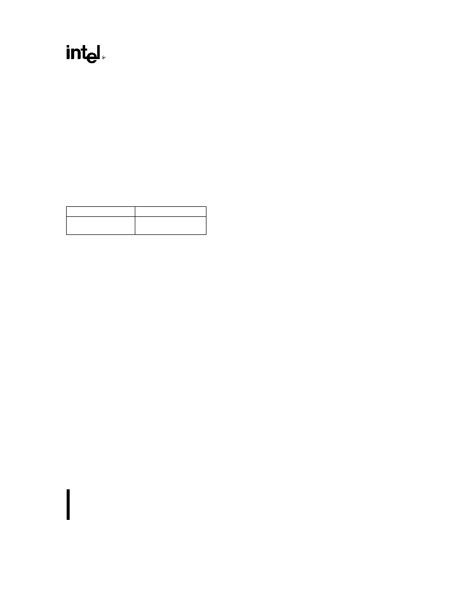
handwriting and diagnostic code Figure 1 shows an
example of a 28F200BL-T application
This increase in software sophistication augments
the probability that a code update will be required
after the PC is shipped The 2-Mbit low power flash
memory products provide an inexpensive update so-
4
28F200BL-T B 28F002BL-T B
lution for the notebook and handheld personal com-
puters while extending their product lifetime Fur-
thermore the 2-Mbit flash memory products' deep
power-down mode provides added flexibility for
these battery-operated portable designs which re-
quire operation at extremely low power levels
The 2-Mbit low power flash products also provide
excellent design solutions for Handy Digital Cellular
Phone applications requiring high density storage
high performance capabilities coupled with low volt-
age operation and a small form factor package (x8-
only bus) The 2-Mbit's blocking scheme allows for
an easy segmentation of the embedded code with
16 Kbytes of Hardware-Protected Boot code 2 Main
Blocks of program code and 2 Parameter Blocks of
8 Kbytes each for frequently updatable data storage
and diagnostic messages (e g phone numbers au-
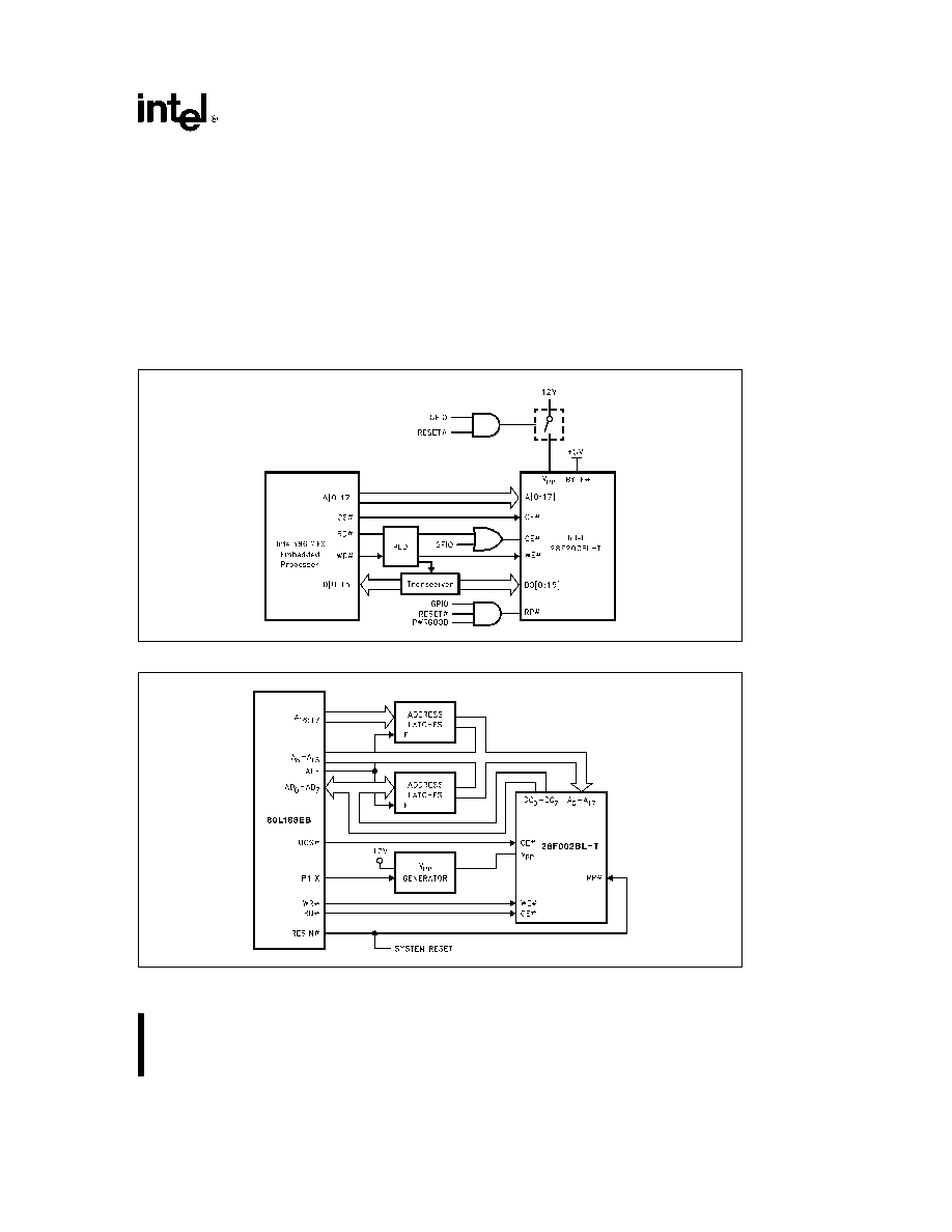
thorization codes) Figure 2 is an example of such an
application with the 28F002BL-T
These are a few actual examples of the wide range
of applications for the 2-Mbit Low Power Boot Block
flash memory family which enables system design-
ers to achieve the best possible product design
Only your imagination limits the applicability of such
a versatile low power product family
290449 ≠ 6
Figure 1 28F200BL-T Interface to Intel386
TM
EX Embedded Processor
290449 ≠ 22
Figure 2 28F002BL-T Interface to INTEL 80L188EB Low Voltage 8-Bit Embedded Microprocessor
5