 | –≠–ª–µ–∫—Ç—Ä–æ–Ω–Ω—ã–π –∫–æ–º–ø–æ–Ω–µ–Ω—Ç: E8870SP | –°–∫–∞—á–∞—Ç—å:  PDF PDF  ZIP ZIP |
Intel
Æ
E8870SP Scalability Port Switch
(SPS) Datasheet
Product Features
s
Scalability Port (SP):
-- Six SPs with 3.2 GB/s peak bandwidth
per direction per SP.
-- Bi-directional SPs for a total bandwidth
of 38.4 GB/s.
s
Integrated Snoop Filter:
-- 1 MB 12-way set associative tag array
capable of maintaining state of 200K
cache lines.
-- Partitioned into four interleaves, each
interleave can be accessed in parallel.
-- Supports up to 266M look-up and
update (LUU) operations per second.
-- Pseudo Least Recently Used (PLRU)
replacement algorithm, with updates on
look-ups and invalidates.
-- ECC coverage, with correction of
single bit errors, detection of double bit
errors.
-- Fast array initialization and/or self test
through configuration register access.
s
Multiple Processor Node Support:
-- Conflict detection logic to maintain
memory consistency for coherent
memory across multiple processor
nodes.
-- Advanced address mapping and decode
capabilities enable flexible routing of
transactions based on address and/or
transaction type.
s
Internal Interconnect:
-- A six-ported dual lane crossbar network
routes transaction packets from one SP
port to another.
-- Separate bypass buses for low latency
snoop look-up and response connection
between ports and interleaves.
s
System Management Bus (SMBus) 2.0
slave interface for server management with
packet error checking.
s
Reliability, Availability, and Serviceability
(RAS):
-- Sideband access to configuration
registers via SMBus or JTAG.
-- End-to-end ECC for all interfaces.
-- Fault detection and logging.
-- Signal connectivity testing via
boundary scan.
s
Packaging:
-- 42.5 mm x 42.5 mm.
-- 1012-pin organic LAN grid array
(OLGA) package-2B.
Document Number: 252034-001
November 2002

ii
Intel
Æ
E8870SP Scalability Port Switch (SPS) Datasheet
INFORMATION IN THIS DOCUMENT IS PROVIDED IN CONNECTION WITH INTEL
Æ
PRODUCTS. NO LICENSE, EXPRESS OR IMPLIED, BY
ESTOPPEL OR OTHERWISE, TO ANY INTELLECTUAL PROPERTY RIGHTS IS GRANTED BY THIS DOCUMENT. EXCEPT AS PROVIDED IN
INTEL'S TERMS AND CONDITIONS OF SALE FOR SUCH PRODUCTS, INTEL ASSUMES NO LIABILITY WHATSOEVER, AND INTEL DISCLAIMS
ANY EXPRESS OR IMPLIED WARRANTY, RELATING TO SALE AND/OR USE OF INTEL PRODUCTS INCLUDING LIABILITY OR WARRANTIES
RELATING TO FITNESS FOR A PARTICULAR PURPOSE, MERCHANTABILITY, OR INFRINGEMENT OF ANY PATENT, COPYRIGHT OR OTHER
INTELLECTUAL PROPERTY RIGHT. Intel products are not intended for use in medical, life saving, or life sustaining applications.
Intel may make changes to specifications and product descriptions at any time, without notice.
Designers must not rely on the absence or characteristics of any features or instructions marked "reserved" or "undefined." Intel reserves these for
future definition and shall have no responsibility whatsoever for conflicts or incompatibilities arising from future changes to them.
The Itanium 2 processor, E8870 chipset, and E8870SP scalability port switch (SPS) may contain design defects or errors known as errata which may
cause the product to deviate from published specifications. Current characterized errata are available on request.
Contact your local Intel sales office or your distributor to obtain the latest specifications and before placing your product order.
Copies of documents which have an order number and are referenced in this document, or other Intel literature, may be obtained by calling1-800-548-
4725, or by visiting Intel's website at http://www.intel.com.
Intel and Itanium are trademarks or registered trademarks of Intel Corporation or its subsidiaries in the United States and other countries.
Copyright © 2002, Intel Corporation. All rights reserved.
*Other names and brands may be claimed as the property of others.

Intel
Æ
E8870SP Scalability Port Switch (SPS) Datasheet
iii
Contents
1
Introduction......................................................................................................................1-1
1.1
Overview ............................................................................................................1-1
1.2
Feature Summary...............................................................................................1-1
1.2.1
Interfaces...............................................................................................1-1
1.2.2
Multinode Routing, Cache Coherency, and Memory Consistency ........1-1
1.2.3
Reliability and Serviceability..................................................................1-1
1.3
SPS Blocks.........................................................................................................1-2
1.3.1
Interleaves.............................................................................................1-2
1.3.2
Ports ......................................................................................................1-3
1.3.3
Interconnect...........................................................................................1-3
1.4
Reference Documents........................................................................................1-3
1.5
Revision History .................................................................................................1-4
2
Signal Descriptions..........................................................................................................2-1
2.1
Conventions .......................................................................................................2-1
2.2
SPS Pin List .......................................................................................................2-2
3
Configuration Registers...................................................................................................3-1
3.1
Access Mechanism ............................................................................................3-1
3.1.1
Conflict Resolution ................................................................................3-1
3.2
Device Mapping..................................................................................................3-1
3.2.1
Assignment of Device Number ..............................................................3-1
3.2.2
Device Mapping Table...........................................................................3-2
3.3
Register Attributes..............................................................................................3-2
3.3.1
SMBus-Initiated Register Access ..........................................................3-3
3.4
SPS Configuration Register Definitions..............................................................3-3
3.5
SPS PCI Standard Configuration Registers ≠ All Functions ..............................3-3
3.5.1
VID: Vendor Identification Register .......................................................3-3
3.5.2
DID: Device Identification Register........................................................3-3
3.5.3
RID: Revision ID Register .....................................................................3-4
3.5.4
CCR: Class Code Register....................................................................3-4
3.5.5
HDR: Header Type Register .................................................................3-5
3.5.6
SVID: Subsystem Vendor Identification Register ..................................3-5
3.5.7
SDID: Subsystem Device Identification Register ..................................3-5
3.6
SP Port Configuration Register ≠ Functions 0:5.................................................3-5
3.6.1
CBC: Chip Boot Configuration...............................................................3-5
3.6.2
SPINCO: SP Interface Control ..............................................................3-7
3.6.3
RECSPPD: Recoverable Error Control Information of SPPD ...............3-9
3.6.4
RECSPL: Recoverable Error Control Information of SPL .....................3-9
3.6.5
REDSPL: Recoverable Error Data Log SPL .........................................3-9
3.6.6
MIR[5:0]: Memory Interleave Range Registers ...................................3-10
3.6.7
SIOH_MAP: SIOH Mapping Register ..................................................3-11
3.6.8
MMIOLS: Memory-Mapped I/O Low Segment Register ......................3-11
3.6.9
MMIOHS: Memory-Mapped I/O High Segment Register ....................3-11
3.6.10 SARS: SAPIC Range Segment Register ............................................3-12
3.6.11 IOPORTS: I/O Space Segment Address.............................................3-12
3.6.12 PSEG: PCI Configuration Bus Segment Address ...............................3-12
3.6.13 CB_PORT: Compatibility Bus Port Number ........................................3-13

iv
Intel
Æ
E8870SP Scalability Port Switch (SPS) Datasheet
3.6.14 VGA_PORT: VGA Port Number..........................................................3-13
3.6.15 PMISC: Port Miscellaneous.................................................................3-13
3.7
SPS Global Registers ≠ Function 6 Only .........................................................3-14
3.7.1
FERRST[1:0]: First Error Status..........................................................3-14
3.7.2
SERRST[1:0]: Two or More Error Status ............................................3-16
3.7.3
ERRMASK[1:0]: ERRST MASK ..........................................................3-16
3.7.4
SPSGLB: SPS Global Register ...........................................................3-16
3.7.5
PERFCON: Performance Monitor Master Control...............................3-17
3.7.6
PMD[1:0]: Performance Monitor Data .................................................3-18
3.7.7
PCMP[1:0]: Performance Monitor Compare........................................3-18
3.7.8
PMR[1:0]: Performance Monitor Response.........................................3-18
3.8
Interleave Configuration Registers ≠ Functions 6 and 7 ..................................3-20
3.8.1
NRESPPC[1:0]: Non-recoverable Error Control Information
of SPPC ..............................................................................................3-21
3.8.2
RECSPPC[1:0]: Recoverable Error Control Information
of SPPC ..............................................................................................3-21
3.8.3
SYS_CFG[1:0]: System Configuration ................................................3-22
3.8.4
ERRCOM[1:0]: Error Command..........................................................3-22
3.8.5
NID_DEF[1:0]: Node ID Definition.......................................................3-23
3.8.6
REM_CDEF[1:0] Remote Component Definition ................................3-23
3.8.7
SFCMD: Snoop Filter Tag/LRU Array Command................................3-24
3.8.8
SFDATA: Snoop Filter Tag/LRU Array Data .......................................3-24
3.8.9
PME[1:0]: Performance Monitor Events ..............................................3-25
4
Address Mapping ............................................................................................................4-1
4.1
Memory Map ...................................................................................................... 4-1
4.1.1
SPS Memory Address Space Regions..................................................4-1
4.1.2
Memory-Mapped I/O Regions ...............................................................4-2
4.1.3
Routing Interrupts.................................................................................. 4-3
4.2
Address Mapping in I/O Space ..........................................................................4-3
4.3
Address Mapping to Access Snoop Filter ..........................................................4-4
4.4
Illegal Addresses ................................................................................................4-4
5
Functional Description.....................................................................................................5-1
5.1
Interfaces ...........................................................................................................5-1
5.1.1
Scalability Port ......................................................................................5-1
5.1.2
JTAG .....................................................................................................5-1
5.1.3
SMBus Interface....................................................................................5-1
5.1.4
GPIO .....................................................................................................5-1
5.2
Snoop Filter ........................................................................................................5-2
5.2.1
Coverage and Addressing.....................................................................5-2
5.2.2
Replacement Algorithm .........................................................................5-3
5.2.3
Snoop Filter Operations and Interfaces ................................................5-3
5.2.4
Error Correction and Logging ................................................................5-4
5.2.5
Snoop Filter Performance .....................................................................5-4
5.3
Interconnect .......................................................................................................5-4
5.3.1
Bypass Buses .......................................................................................5-4
5.3.2
Crossbar Switch ....................................................................................5-5
6
Clocking .......................................................................................................................... 6-1
6.1
SPS Reference Clock (SYSCLK) .......................................................................6-1
6.2
Other Functional and Electrical Requirements...................................................6-1

Intel
Æ
E8870SP Scalability Port Switch (SPS) Datasheet
v
6.2.1
Spread Spectrum Support.....................................................................6-1
6.2.2
No Stop Clock or Thermal Shutdown ....................................................6-1
6.2.3
SMBus Clocking ....................................................................................6-1
6.2.4
JTAG Test Access Port .........................................................................6-1
7
Reliability, Availability and Serviceability.........................................................................7-1
7.1
Data Integrity ......................................................................................................7-1
7.1.1
End-to-End Error Detection ...................................................................7-1
7.1.2
Error Reporting ......................................................................................7-2
7.1.3
Interface Details ....................................................................................7-3
7.1.4
Time-out ................................................................................................7-3
8
Electrical Specification ....................................................................................................8-1
8.1
Non-operational Maximum Rating......................................................................8-1
8.2
Operational Power Delivery Specification ..........................................................8-1
8.3
Scalability Port Signal Group..............................................................................8-2
8.4
SMBus and TAP Electrical Specifications ..........................................................8-2
8.5
DC Specifications ...............................................................................................8-3
8.6
AC Specifications ...............................................................................................8-4
8.6.1
AC Timing Waveforms ..........................................................................8-5
8.7
Miscellaneous Signal Pins..................................................................................8-6
8.7.1
Signal Groups........................................................................................8-6
8.7.2
DC Characteristics ................................................................................8-7
8.8
AC Specification .................................................................................................8-8
8.9
Intel
Æ
E8870 Chipset Clock Signal Groups ........................................................8-9
9
Ballout and Package Information ....................................................................................9-1
9.1
1012-Ball OLGA2b Package Information ...........................................................9-1
10
Testability ......................................................................................................................10-1
10.1
Test Access Port ..............................................................................................10-1
10.1.1 The TAP Logic.....................................................................................10-1
10.1.2 Accessing the TAP Logic ....................................................................10-2
10.2
Public TAP Instructions ....................................................................................10-4
10.3
TAP Registers ..................................................................................................10-5
Figures
1-1
SPS Block Diagram............................................................................................1-2
4-1
System Memory Address Space ........................................................................4-1
4-2
Example of Mapping MMIO Regions..................................................................4-3
8-1
TAP DC Thresholds ...........................................................................................8-4
8-2
TAP and SMBus Valid Delay Timing Waveform ................................................8-5
8-3
TCK and SM_CLK Clock Waveform ..................................................................8-6
9-1
1012-Ball OLGA2b Package Dimensions ≠ Top View .......................................9-1
9-2
1012-Ball OLGA2b Package Dimensions ≠ Bottom View ..................................9-2
9-3
1012-Ball OLGA2b Solder Ball Detail.................................................................9-3
10-1
TAP Controller Signals .....................................................................................10-1
10-2
Simplified Block Diagram of TAP Controller.....................................................10-2
10-3
TAP Controller State Diagram..........................................................................10-3
10-4
TAP Instruction Register ..................................................................................10-6

vi
Intel
Æ
E8870SP Scalability Port Switch (SPS) Datasheet
Tables
2-1
Buffer Technology Types ...................................................................................2-1
2-2
Buffer Signal Directions......................................................................................2-1
2-3
Signal Naming Conventions ...............................................................................2-2
2-4
SPS Pin List .......................................................................................................2-2
3-1
Configuration Address Bit Mapping....................................................................3-1
3-2
Function Maps....................................................................................................3-2
3-3
Register Attributes Definitions ............................................................................3-2
3-4
Register Range for Functions 6 and 7 .............................................................3-20
3-5
Control: Snoop Filter ECC Error Fields ............................................................3-21
4-1
Regions of Transactions to Decode ...................................................................4-2
4-2
I/O Space Mappings...........................................................................................4-4
4-3
SPS Transactions to Illegal Addresses .............................................................. 4-4
5-1
Example SF Coverage for Different Node/L3 Configurations ............................5-2
5-2
Physical Address Partitioning.............................................................................5-3
5-3
Snoop Filter Entry ..............................................................................................5-3
8-1
Absolute Maximum Non-operational DC Ratings at the Package Pin ...............8-1
8-2
Voltage and Current Specifications....................................................................8-1
8-3
Scalability Port Interface Signal Group .............................................................. 8-2
8-4
SMBus and TAP Interface Signal Group............................................................8-3
8-5
TAP Signal Terminations ...................................................................................8-3
8-6
TAP DC Parameters .........................................................................................8-3
8-7
SMBus DC Parameters ......................................................................................8-4
8-8
SMBus Signal Group AC Specifications ...........................................................8-4
8-9
TAP Signal Group AC Specifications ................................................................8-5
8-10
Signal Groups ....................................................................................................8-6
8-11
CMOS 1.3V DC Parameters ..............................................................................8-7
8-12
CMOS 1.5V OD DC Parameters .......................................................................8-7
8-13
CMOS 1.5V DC Parameters ..............................................................................8-7
8-14
CMOS 1.3V AC Parameters .............................................................................8-8
8-15
CMOS 1.5V Open-Drain AC Parameters ...........................................................8-8
8-16
CMOS 1.5V AC Parameters ..............................................................................8-8
8-17
Clock Signal Groups ..........................................................................................8-9
8-18
LVHSTL Clock DC Parameters..........................................................................8-9
9-1
SPS Ball List ...................................................................................................... 9-4
9-2
SPS Signal List ................................................................................................9-17
10-1
TAP Signal Definitions .....................................................................................10-1
10-2
Public TAP Instructions ....................................................................................10-4
10-3
Example of Configuration Access Data Register Format.................................10-6

Intel
Æ
E8870SP Scalability Port Switch (SPS) Datasheet
1-1
Introduction
1
1.1
Overview
The Scalability Port Switch (SPS) component provides the interconnect and coherency support for
building multinode, multiprocessor systems with the Intel
Æ
E8870 chipset. It has six Scalability
Port (SP) interfaces that provide physical and logical connections to the Scalable Node Controller
(SNC) and Server Input/Output Hub (SIOH) components.
The SPS has an integrated snoop filter (SF) that is used to track the state of cached lines in the
system. The SP coherency protocol and the SF are used by the SPS to maintain cache coherency
and memory consistency in multinode systems.
1.2
Feature Summary
1.2.1
Interfaces
∑
Six simultaneous bi-directional (SBD) SP interfaces (each port supporting up to 3.2 GB/s peak
bandwidth in each direction).
∑
Access to internal control and status registers via TAP port (i.e. JTAG) and System
Management Bus (i.e. SMBus).
1.2.2
Multinode Routing, Cache Coherency, and Memory
Consistency
∑
An integrated SF tag array capable of maintaining state of 200K cache lines. In a system with
two SPS components, this is equivalent to 2X coverage for a system with eight Intel
Æ
Itanium
Æ
2 processors with 3 MB of L3 cache per processor.
∑
A single SPS can support up to 266 SF mega look-up and update (MLUU) operations per
second.
∑
Includes support for 128 byte cache lines, and different L3 cache state transitions.
∑
Conflict detection to maintain memory consistency for coherent memory across multiple
nodes.
∑
Address mapping and decode capabilities that enable flexible routing of transactions based on
address and/or transaction type.
1.2.3
Reliability and Serviceability
∑
ECC generation/detection/correction on accesses to and from configuration space, and ECC
coverage on the SF tag array.
∑
Link-level retry support on all SP interfaces.
∑
Signal connectivity testing via boundary scan.
Introduction
1-2
Intel
Æ
E8870SP Scalability Port Switch (SPS) Datasheet
1.3
SPS Blocks
1.3.1
Interleaves
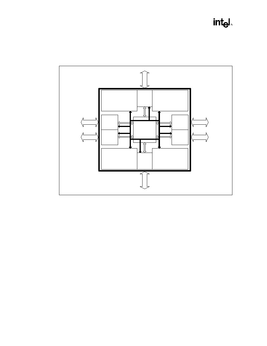
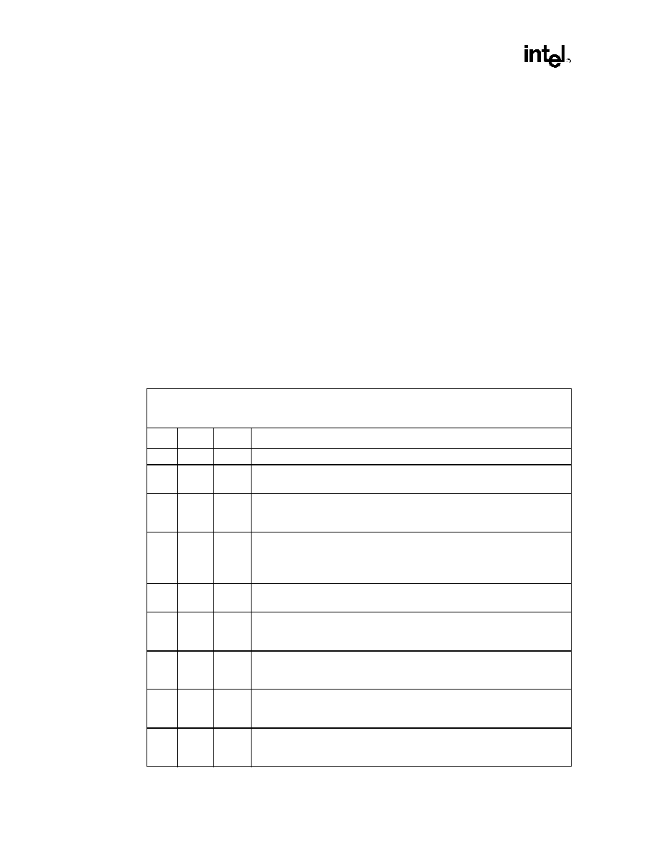
The SPS coherency protocol logic is divided into four interleaves. Each interleave consists of a
portion of the SF tag array and a Scalability Port Protocol Central (SPPC) block. Transactions are
directed to an interleave based on address and transaction type. Each interleave can operate in
parallel.
The SF is a 12-way set associative array, with each interleave containing 4K sets, for a total of 16K
sets per SPS. Each SF entry contains an address tag, the state of the cache line, and a presence
vector identifying the nodes that have the line cached. The replacement algorithm for the SF is
Pseudo Least Recently Used (PLRU), with modifications to support updates based on replacement
information received from the processors. Each SF interleave can support 66 MLUU/s, for a total
SPS throughput of 266 MLUU/s. Each system bus request results in one LUU operation in the SF.
A SPPC block is associated with each SF partition. As the name implies, the SPPC generates a
sequence of operations or transactions based on the type of request as defined by the SP Protocol.
For coherent transactions, the SF is accessed, and address conflicts are checked and handled.
The SPPC may retry transactions or assert back pressure to the SP due to conflicts or resource
limitations. The SPPC may generate snoop requests to remote nodes, invalidation requests or read
requests in response to coherent memory requests. The SPPC also handles transactions that require
special handling such as broadcast or sequencing.
Figure 1-1. SPS Block Diagram
001333
SPPC/SF Interleave 0
SPPC/SF Interleave 2
SP Port 1
SP Port 0
SP Port 3
SP Port 2
SPPC/SF Interleave 3
SP/
SPP
D
SP
/
S
PPD
SPPC/SF Interleave 1
Port 4
Port 5
Port 0
Port 1
Port 2
Port 3
X-Bar
Bypass
Bypass
SP Po
rt
5
SP
Po
r
t
4
SP/SPPD
SP/SPPD
SP/SPPD
SP/SPPD

Intel
Æ
E8870SP Scalability Port Switch (SPS) Datasheet
1-3
Introduction
1.3.2
Ports
The SPS has six SPs. Each port consists of a SP block and a Scalability Port Protocol Distributed
(SPPD) block.
The SP block implements the physical layer and link layer of the SP protocol. This interface is
common between all components of the E8870 chipset.
Upon receiving a packet from the SP, the SPPD decodes the header to determine how the packet
should be routed in the SPS. The SPPD routes coherent requests to the appropriate SF interleave
based on address. For some coherent requests, requests may be spawned directly by the SPPD and
sent to the home node. For non-coherent and special transactions, attribute encodings and address
decode are used to determine the packet destination. For responses, packets may be routed to either
the SPPC, or to another port based on information in the packet header. The SPPD also provides
the data path for requests and responses that have data. The SPPD only asserts back pressure to the
SP due to resource limitations.
The six SPs are logically identical. However, the pinout of two of the ports are oriented differently.
This is to enable at least one system configuration where the SPs can be connected without doing
any swizzling of wires on the board.
1.3.3
Interconnect
The SPS uses bypass buses to route request and response packets between the SPPD and SPPC
blocks. This improves performance by "bypassing" the crossbar and decreasing latency. The
bypass buses carry packets from the SPPDs to the SPPCs and from the SPPCs to the SPPDs. Each
pair of SPPD_to_C and SPPC_to_D bypass buses is shared by three ports and two SPPCs. Each
bus can support up to 200 MT/s. The bypass buses can support a maximum of 800 MT/s from all
the ports to the SPPCs, assuming evenly distributed traffic.
A six-ported crossbar switch is also used to route packets from one SP port to another across the
SPS. The crossbar switch has two lanes per port; one allocated to requests, and the other to
responses. Each crossbar port can send and receive data at the full SP port bandwidth.
1.4
Reference Documents
∑
Intel
Æ
E8870 Scalable Node Controller (SNC) Datasheet
∑
Intel
Æ
E8870DH DDR Memory Hub (DMH) Datasheet
∑
Intel
Æ
E8870IO Server I/O Hub (SIOH) Datasheet
∑
Intel
Æ
82870P2 64-bit Hub 2 (P64H2) Datasheet
∑
Intel
Æ
82801DB I/O Controller Hub4 (ICH4) Datasheet
∑
SMBus Specification, Revision 2.0
∑
PCI Local Bus Specification, Revision 2.2
∑
PCI-X Local Bus Specification, Revision 1.0

Introduction
1-4
Intel
Æ
E8870SP Scalability Port Switch (SPS) Datasheet
1.5
Revision History
Revision
Number
Description
Date
-001
Initial release of the document.
November 2002

Intel
Æ
E8870SP Scalability Port Switch (SPS) Datasheet
2-1
Signal Descriptions
2
2.1
Conventions
The terms assertion and deassertion are used extensively when describing signals, to avoid
confusion when working with a mix of active-high and active-low signals. The term assert, or
assertion, indicates that the signal is active, independent of whether the active level is represented
by a high or low voltage. The term deassert, or deassertion, indicates that the signal is inactive.
Signal names may or may not have a "#" appended to them. The "#" symbol at the end of a signal
name indicates that the active, or asserted state occurs when the signal is at a low voltage level.
When "#" is not present after the signal name the signal is asserted when at the high voltage level.
When discussing data values used inside the component, the logical value is used. For instance.,a
data value described as "1101b" would appear as "1101b" on an active-high bus, and as "0010b"
on an active-low bus. When discussing the assertion of a value on the actual signal, the physical
value is used; i.e. asserting an active-low signal produces a "0" value on the signal.
Table 2-1
and
Table 2-2
list the reference terminology used later for buffer technology types (e.g.
SBD, etc.) and buffering signal types (e.g. input, output, etc.).
Some signals or groups of signals have multiple versions. These signal groups may represent
distinct, but similar, ports or interfaces or they may represent identical copies of the signal used to
reduce loading effects.
Table 2-3
shows the conventions the SPS uses
.
Table 2-1. Buffer Technology Types
Buffer Type
Description
SBD
Simultaneous bi-directional.
Differential
A differential input that requires a voltage reference or
the signal compliment.
SPCMOS
CMOS type I/O with Schmidt trigger input.
CMOS OD
CMOS open drain I/O.
SMBus OD
SMBus open drain I/O with Schmidt trigger input with a
voltage level of 3.3V and max. frequency of 100 KHz.
JTAG
1.5V JTAG I/O.
Analog
Typically a voltage reference or specialty power supply.
Table 2-2. Buffer Signal Directions
Buffer Direction
Description
I
Input pin.
O
Output pin.
I/O
Bi-directional (input/output) pin.
Signal Descriptions
2-2
Intel
Æ
E8870SP Scalability Port Switch (SPS) Datasheet
Typically, upper case groups (e.g. "A, B, C") represent functionally similar, but logically distinct,
signals. Each signal provides an independent control, and may or may not be asserted at the same
time as the other signals in the grouping. In contrast, lower case groups, (e.g. "a, b, c") typically
represent identical duplicates of a common signal. Such duplicates are provided to reduce loading.
2.2
SPS Pin List
Table 2-3. Signal Naming Conventions
Convention
Expands to
RR{0/1/2}XX
Expands to: RR0XX, RR1XX, and RR2XX.
RR[2:0]
Denotes a bus and expands to: RR2, RR1, and RR0.
RR# or RR[2:0]#
Denotes an active low signal or bus.
Table 2-4. SPS Pin List
Signal
Type
Frequency
Description
Scalability Ports ≠ 72 Pins Total each Port
SP{0/1/2/3/4/5}ZUPD[1:0]
I
Analog
N/A
Impedance Update: Used to adjust the
impedance of I/O drivers.
SP{0/1/2/3/4/5}SYNC
I/O
SPCMOS
N/A
Reset Synchronization: Provides
synchronization between ports for impedance
control and reference voltage adjustment. This
signal is also used by the SP reset logic to
determine when SP comes out of reset.
SP{0/1/2/3/4/5}SYNC is released when ports at
both ends of the link are ready.
SP{0/1/2/3/4/5}PRES
I
SPCMOS
N/A
Scalability Port Present: Signals the Scalability
Port of an impending hot plug event.
SP{0/1/2/3/4/5}AVREFH[3:0]
I
Analog
N/A
Strand A Voltage Reference: 3/4 VCC
Reference.
SP{0/1/2/3/4/5}AVREFL[3:0]
I
Analog
N/A
Strand A Voltage Reference: 1/4 VCC
Reference.
SP{0/1/2/3/4/5}ASTBP[1:0]
I/O
SBD
400 MHz
P Strobes: Positive phase data strobes for
strand A to transfer data at the 2x rate
(800 MHz).
SP{0/1/2/3/4/5}ASTBN[1:0]
I/O
SBD
400 MHz
N Strobes: Negative phase data strobes for
strand A to transfer data at the 2x rate
(800 MHz).
SP{0/1/2/3/4/5}AD[15:0]
I/O
SBD
800 MHz
Data Bus: 16 bits of the data portion of a PHIT
on strand A (D[15:0]). These bits are SSO
encoded. SP{0/1/2/3/4/5}ASSO determines if
these are out of an inverter or not.
SP{0/1/2/3/4/5}AEP[2:0]
I/O
SBD
800 MHz
Parity/ECC: Two of these signals carry the ECC
information for the data flits. There are four bits of
ECC for each data PHIT. The header flits are not
ECC protected. The third signal is for parity. Each
PHIT is always protected by two bits of parity.
AEP[1:0] is GEP[1:0] and AEP[2] is TEP[0].
SP{0/1/2/3/4/5}ALLC
I/O
SBD
800 MHz
Link Layer Control: For each PHIT these
signals carry two of the four bits of link layer
control information.

Intel
Æ
E8870SP Scalability Port Switch (SPS) Datasheet
2-3
Signal Descriptions
Scalability Ports ≠ 72 Pins Total each Port (Continued)
SP{0/1/2/3/4/5}ASSO
I/O
SBD
800 MHz
SSO Encode: This signal is asserted to indicate
that the data bits over Strand A are inverted.
SP{0/1/2/3/4/5}ARSVD
I/O
SBD
N/A
Reserved
SP{0/1/2/3/4/5}BVREFH[3:0]
I
Analog
N/A
Strand B Voltage Reference:
3/4 VCC Reference.
SP{0/1/2/3/4/5}BVREFL[3:0]
I
Analog
N/A
Strand B Voltage Reference:
1/4 VCC Reference.
SP{0/1/2/3/4/5}BSTBP[1:0]
I/O
SBD
400 MHz
P Strobes: Positive phase data strobes for
strand B to transfer data at the 2x rate
(800 MHz).
SP{0/1/2/3/4/5}BSTBN[1:0]
I/O
SBD
400 MHz
N Strobes: Negative phase data strobes for
strand B to transfer data at the 2x rate
(800 MHz).
SP{0/1/2/3/4/5}BD[15:0]
I/O
SBD
800 MHz
Data Bus: 16 bits of the data portion of a PHIT
on strand B (D[31:16]). These bits are SSO
encoded. SP{0/1/2/3/4/5}BSSO determines if
these are out of an inverter or not.
SP{0/1/2/3/4/5}BEP[2:0]
I/O
SBD
800 MHz
Parity/ECC: Two of these signals carry the ECC
information for the data flits. There are four bits of
ECC for each data PHIT. The header flits are not
ECC protected. The third signal is for parity. Each
PHIT is always protected by two bits of parity.
BEP[1:0] is GEP[3:2] and BEP[2] is TEP[1].
SP{0/1/2/3/4/5}BLLC
I/O
SBD
800 MHz
Link Layer Control: For each PHIT these
signals carry two of the four bits of link layer
control information.
SP{0/1/2/3/4/5}BSSO
I/O
SBD
800 MHz
SSO Encode: This signal is asserted to indicate
that the data bits over Strand B are inverted.
SP{0/1/2/3/4/5}BRSVD
I/O
SBD
N/A
Reserved
Clocking ≠ 5 Pins Total
SYSCLK
I
Differential
200 MHz
SYS Clock: This is the 200 MHz differential clock
reference input to the SPS core. The system
board logic generates this signal.
SYSCLK#
I
Differential
200 MHz
SYS Clock Complement: 200 MHz Clock
Complement.
LVHSTLODTEN
I
CMOS
N/A
On-die Termination: SYSCLK and SYSCLK#
on-die termination enable.
VCCA
I
Analog
N/A
Analog VCC Voltage.
VSSA
I
Analog
N/A
Analog VSS Voltage.
System Management ≠ 3 Pins Total
SCL
I/O
SMBus OD
SCL
SMBus Clock: Provides synchronous operation
of the SMBus bus.
SDA
I/O
SMBus OD
SCL
SMBus Addr/Data: Used for data transfer and
arbitration on the SMBus bus.
VCC33
Analog
N/A
Vcc3.3: Voltage reference for 3.3v I/Os.
Table 2-4. SPS Pin List (Continued)
Signal
Type
Frequency
Description

Signal Descriptions
2-4
Intel
Æ
E8870SP Scalability Port Switch (SPS) Datasheet
Performance, Debug, and Error Signals ≠ 33 Pins Total
SP{0/1/2/3/4/5}GPIO[1:0]
I/O
CMOS OD
N/A
Scalability Port General Purpose I/O:
These signals could be used to route sideband
signals for domains in multinode systems.
NODEID[2:0]
I
CMOS
N/A
Node ID: Strap bits that indicate the Node ID of
this SPS. The NODEID is captured on the rising
edge of hard reset. The captured value is sent on
the IDLE flits. NODEID[4:3] should always be set
to "11".
BPOUT
O
CMOS
200 MHz
Breakpoint Input: Breakpoint and Performance
Monitoring Output signal.
BPIN
I
CMOS
200 MHz
Breakpoint Output: Breakpoint and
Performance Monitoring Input signal.
DBG[3:0]#
O
CMOS
200 MHz
Event Output Signals.
ERRD0[2:0]#
I/O
CMOS OD
50 MHz
Error Code Signals Domain 0: These signals
carry encoded error information from SPS.
These reflect recoverable and non-recoverable
errors detected by SPS. The system
management logic can examine these
independent of the operating system.
The output value will be asserted until the
software clears the error in the error register.
ERRD1[2:0]#
I/O
CMOS OD
50 MHz
Error Code Signals Domain 1: These signals
carry encoded error information from SPS.
These reflect recoverable and non-recoverable
errors detected by SPS. The system
management logic can examine these
independent of the operating system.
The output value will be asserted until the
software clears the error in the error register.
EV[3:0]#
I/O
CMOS OD
50 MHz
Event External Inputs: These signals are driven
and sampled by the performance monitor unit in
SPS and are used by the system debug logic. As
inputs these signals are driven by the debug logic
to the performance monitor unit.
INT_OUT[1:0]#
O
CMOS OD
50 MHz
Interrupt Request: This signal is asserted by
SPS.
TDIOAnode
I/O
Analog
N/A
Thermal Diode Anode: This is the anode of the
thermal diode.
TDIOCathode
I/O
Analog
N/A
Thermal Diode Cathode: This is the cathode of
the thermal diode.
Table 2-4. SPS Pin List (Continued)
Signal
Type
Frequency
Description

Intel
Æ
E8870SP Scalability Port Switch (SPS) Datasheet
2-5
Signal Descriptions
Reset ≠ 4 Pins Total
PWRGOOD
I
CMOS
N/A
Power Good: This signal is held low until all
power supplies are in specification. This signal is
followed by RESETI# deassertion.
RESETI#
I
CMOS
N/A
Reset Input: This is the hard reset input to the
SPS.
RESETID#[1:0]
I
CMOS
N/A
Reserved
Test Access Port (JTAG) ≠ 5 Pins Total
TCK
I
JTAG
TCK
JTAG Test Clock: Clock input used to drive Test
Access Port (TAP) state machine during test and
debugging.
TDI
I
JTAG
TCK
JTAG Test Data In: Data input for test mode.
Used to serially shift data and instructions into
TAP.
TDO
O
JTAG
TCK
JTAG Test Data Out: Data: Data output for test
mode. Used to serially shift data out of the
device.
TMS
I
JTAG
TCK
JTAG Test Mode Select: This signal is used to
control the state of the TAP controller.
TRST#
I
JTAG
N/A
JTAG Test Reset: This signal resets the TAP
controller logic.
Table 2-4. SPS Pin List (Continued)
Signal
Type
Frequency
Description

Signal Descriptions
2-6
Intel
Æ
E8870SP Scalability Port Switch (SPS) Datasheet
Intel
Æ
E8870SP Scalability Port Switch (SPS) Datasheet
3-1
Configuration Registers
3
3.1
Access Mechanism
The E8870 chipset supports PCI configuration space access as defined in the PCI Local Bus
Specification, Revision 2.2. The internal registers of this chipset can be accessed in Byte, Word
(16-bit), or Dword (32-bit) quantities, with the exception of CONFIG_ADDRESS, which can only
be accessed as a Dword. All mult-byte numeric fields use "little-endian" ordering (i.e. lower
addresses contain the least significant parts of the field).
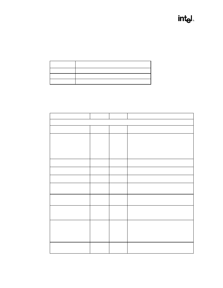
Address mapping from the SP, SMBus port, and JTAG interface are defined in
Table 3-1
.
3.1.1
Conflict Resolution
The SPS accepts configuration register reads and writes through three mechanisms. There are two
serial mechanisms: SMBus and JTAG. Accesses initiated by other SNCs or SIOHs appear as
Configurations reads and writes on the SPs.
Multiple configuration accesses arriving on a SP are handled one at a time, and back pressure may
be asserted on the SP. Accesses arriving on different SPs, the SMBus port, and the JTAG interface
are handled one at a time, in any order. Requests are serviced in a round-robin manner.
3.2
Device Mapping
3.2.1
Assignment of Device Number
BUS[7:0] are set to 0xFFh and NodeID[4:3] are hardwired to 0x3 on the SPS. NodeID[2:0] are
captured from external pins on the SPS. Information captured from the idle flits is valid only when
the idle detection bit in the SP Interface Control Register (SPINCO) register is set. As a
convention, an invalid port will have the same NodeID as the SPS.
BUS[7:0] and NodeID[4:0] (only NodeID[2:0] for SPS) are captured and saved in the Chip Boot
Configuration (CBC) register. The power-up strappings are included in the SP idle packet.
Information captured in the CBC register is valid only when the idle detection bit in register
Table 3-1. Configuration Address Bit Mapping
PCI Configuration
Space
SP Configuration
Read/write
JTAG Configuration
Register
SMBus Configuration
Registers
Bus[7:0]
A[23:16]
BusNumber[7:0]
BusNumber[7:0]
Device[4:0]
A[15:11]
DeviceID[4:0]
Dev[4:0]
Function[2:0]
A[10:8]
FunctionNumber[2:0]
Func[2:0]
Register[5:1]
A[7:3]
RegisterAddress[5:1]
Reg[5:1]
Register[0]
ReqType[0]
RegisterAddress[0]
Reg[0]
ByteEn[3:0]
BE[7:4]
Command (Decoded)
Command (Decoded)
Reserved
A[43:24]=0, SPS ignores
N/A
N/A

Configuration Registers
3-2
Intel
Æ
E8870SP Scalability Port Switch (SPS) Datasheet
SPINCO is set. Any transactions routed to a SP whose idle flit detection bit is not set is master-
aborted. Each chip uses the contents of register CBC to decide whether a configuration access is
targeted to it or not. The two SPS's can be assigned the same device number upon reset. The
configuration spaces of the SPS's are accessed by setting the "Default SP" bit in the SPINCO
register or the CBC registers of SIOH and SNC. The initialization software assigns different device
numbers to the two SPSs.
SPS routes configuration accesses based upon the PSEG (PCI bus segment register) and the per-
port CBC register. After reset, only one entry in each port's CBC register is valid. The valid entry is
selected by the function number. For example, SP3 NodeID and BUS is valid upon reset only in
function 3. BIOS/SAL/PAL must copy those valid entries into all ports so that configuration writes
and reads can be routed to other components.
3.2.2
Device Mapping Table
The device number for each component of this chipset can be anywhere between 0 and 31 (refer to
Table 3-2
). PAL/SAL must probe the system to find where each component is located.
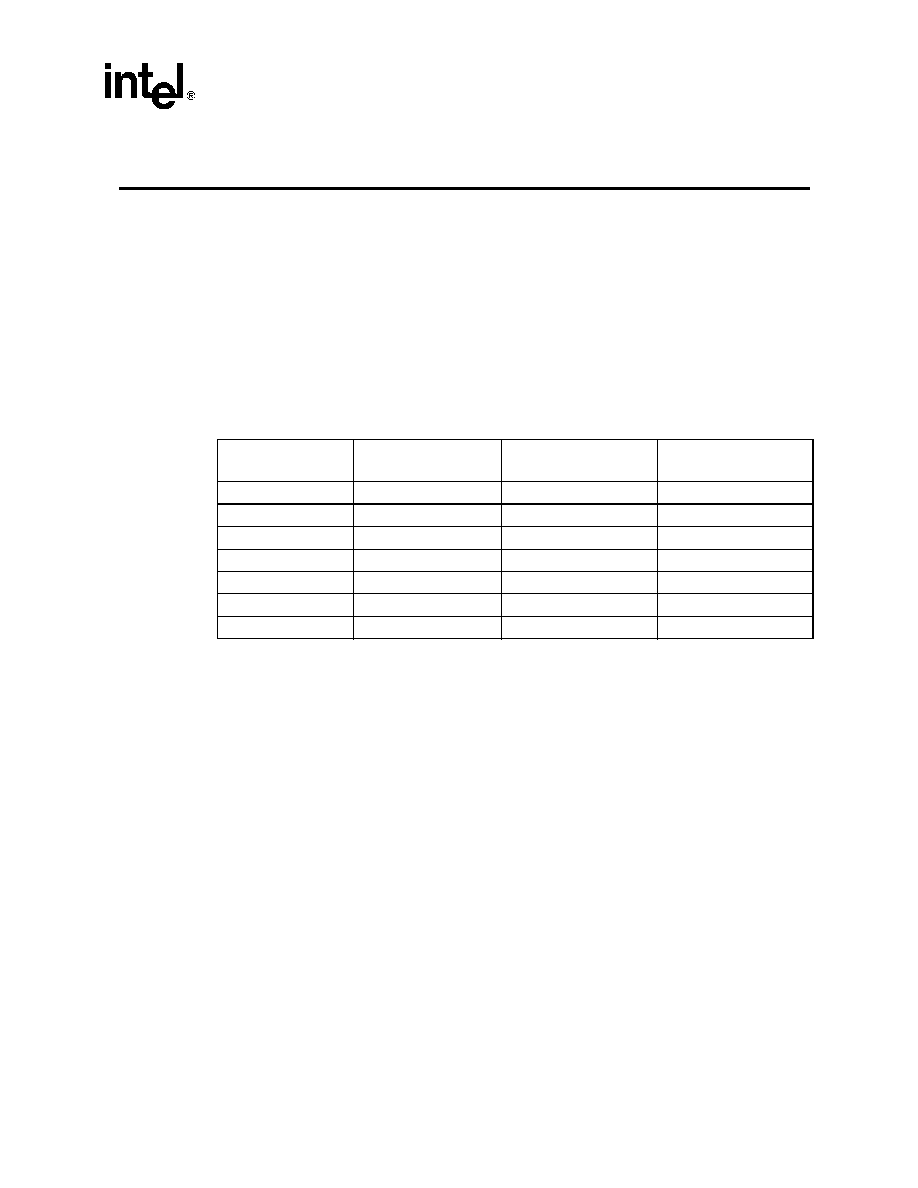
3.3
Register Attributes
The Default column in the following register definitions (refer to
Table 3-3
) indicates that the
register will be set to this value after a hard reset. Start-up BIOS software is responsible for setting
all register values that are dependent on the particular platform. Each of the following registers
uses the following conventions for the bit attribute column.
Table 3-2. Function Maps
Device/Function
Description
SPS Function 0:5
Registers for port 0, 1, 2, 3, 4, 5.
SPS Function 6
Registers for interleaves 0 and 1 (bi-interleave 0) and global registers that are
neither per-port nor per-interleave.
SPS Function 7
Registers for interleaves 2 and 3 (bi-interleave 1).
Table 3-3. Register Attributes Definitions
Attribute
Abbreviation
Description
Read Only
RO
The bit is set by the hardware only; software can only read the bit. Writes to the
register have no effect. A hard reset sets the bit to its default value.
Read/Write
RW
The bit can be read or written by software. A hard reset sets the bit to its default
value.
Read/Clear
RC
The bit can be either read or cleared by software. In order to clear a RC bit, the
software must write a one to it. Writing a zero to an RC bit will have no effect. A
hard reset sets the bit to its default value.
Sticky
RWS, RCS,
ROS
The bit is "sticky" or unchanged by a hard reset. Read/Write, Read/Clear and
Read Only bits may be sticky. These bits can only be cleared by a PWRGOOD
reset.
Write Once
W1
Only the first write has an effect. Cleared by reset.
Reserved
RV
This bit is reserved for future expansion and must not be written. The PCI Local
Bus Specification, Revision 2.2 requires that reserved bits must be preserved.
Any software that modifies a register containing a reserved bit is responsible for
reading the register, modifying the desired bits, and writing back the result.
Intel
Æ
E8870SP Scalability Port Switch (SPS) Datasheet
3-3
Configuration Registers
3.3.1
SMBus-Initiated Register Access
The SPS claims addresses 1110_XXX, where XXX specifies NODEID[2:0] pin strappings
(sampled upon the deassertion of RESETI#).
3.4
SPS Configuration Register Definitions
The following register definitions are accessed through the standard PCI mechanism (See
Section 3.1, "Access Mechanism."
) The SPS is not a fully PCI compliant device, but the register
map is defined with the intent to be as similar to PCI devices as possible. This is to help software
stay as consistent as possible. Some PCI header registers are defined and the remaining
configuration registers reside above 40h.
Unimplemented registers return all zeros when read. Writes to unimplemented registers are
ignored, and return with a normal completion status.
3.5
SPS PCI Standard Configuration Registers ≠ All
Functions
Writes to unimplemented and reserved registers will have no effect. Reads to unimplemented and
reserved registers will return a data value of 0. These accesses will complete normally (no master
abort).
The first group of registers in this section define the necessary standard PCI registers.
3.5.1
VID: Vendor Identification Register
The VID Register contains the vendor identification number, which identifies the manufacturer of
the device. This 16-bit register, combined with the Device Identification Register, uniquely
identifies any PCI device. Writes to this register have no effect.
3.5.2
DID: Device Identification Register
This 16-bit register, combined with the Vendor Identification register, uniquely identifies the SPS.
Writes to this register have no effect.
Device:
Node_ID
Function: 0-7
Offset:
00h
Bit
Attr
Default
Description
15:0
RO
8086h
Vendor Identification Number: This is a 16-bit value assigned to Intel. Intel VID =
8086h.

Configuration Registers
3-4
Intel
Æ
E8870SP Scalability Port Switch (SPS) Datasheet
3.5.3
RID: Revision ID Register
The Revision ID register tracks the specific revision of this component. Since this register is part of
the standard PCI header, there is a RID register per PCI function.
3.5.4
CCR: Class Code Register
The Class Code register identifies the SPS component as a host bridge. This register adheres to the
PCI Local Bus Specification, Revision 2.2. Since this register is part of the standard PCI header,
there is a CCR register per PCI function.
Device:
Node_ID
Function: 0-7
Offset:
02h
Bit
Attr
Default
Description
15:0
RO
F0:0x0530
F1:0x0531
F2:0x0532
F3:0x0533
F4:0x0534
F5:0x0535
F6:0x0536
F7:0x0537
Device Identification Number: This value is the device ID for the SPS
component. In order for proper driver functionality, each SPS function has a
different value for the DID register.
Device:
Node_ID
Function: 0-7
Offset:
08h
Bit
Attr
Default
Description
7:0
RO
10h
Revision Identification Number: For the B-0 stepping of the SPS, this value is
10H.
Device:
Node_ID
Function: 0-7
Offset:
09h
Bit
Attr
Default
Description
23:16
RO
06h
Base Class Code: This code indicates that the SPS is a bridge device.
15:8
RO
00h
Sub-Class Code: This code indicates that the SPS bridge is part of a host bridge.
7:0
RO
00h
Register-Level Programming Interface: This field identifies a specific
programming interface that device independent software can use to interact with
the device. There are no such interfaces defined for host bridges.
Intel
Æ
E8870SP Scalability Port Switch (SPS) Datasheet
3-5
Configuration Registers
3.5.5
HDR: Header Type Register
This register identifies the header layout of the configuration space. Writes to this register have no
effect.
3.5.6
SVID: Subsystem Vendor Identification Register
This register contains the subsystem vendor identification number. It is programmed by software
and assists in software in future activities such as driver selection. Only the first write to this
register has any affect.
3.5.7
SDID: Subsystem Device Identification Register
This register contains the subsystem device ID. Only the first write to this register has any affect.
3.6
SP Port Configuration Register ≠ Functions 0:5
3.6.1
CBC: Chip Boot Configuration
SPS routes configuration accesses based upon the per-port PCI bus range (bus_start:bus_end) and
the per-port CBC register. After reset, only one entry in each port's CBC register is valid. The valid
entry is selected by the function number. For example, SP3 NodeID and BUS is valid upon reset
only in function 3. BIOS/SAL/PAL must copy those valid entries into all ports so that
configuration reads and writes can be routed.
Device:
NodeID
Function: 0-7
Offset:
0Eh
Bit
Attr
Default
Description
7
RO
1
Multi-function Device: Selects whether this is a multi-function device, that may
have alternative configuration layouts. The SPS has more than the 256 bytes of
configuration registers allotted to a single function. Therefore, the SPS is defined to
be a multifunction device, and this bit is hardwired to 1.
6:0
RO
00h
Configuration Layout: This field identifies the format of the 10h through 3Fh space.
The SPS uses header type "00".
Device:
NodeID
Function: 0-7
Offset:
2Ch
Bit
Attr
Default
Description
15:0
W1
8086
Subsystem Vendor Identification Number: This value is the subsystem vendor ID
for the SIOH component. The value can only be assigned once after reset.
Device:
NodeID
Function: 0-7
Offset:
2Eh
Bit
Attr
Default
Description
15:0
W1
0h
Subsystem Device Identification Number.

Configuration Registers
3-6
Intel
Æ
E8870SP Scalability Port Switch (SPS) Datasheet
To save register bits, BUS[7:0] are hardwired to FFh and NodeID[4:3] are hardwired to 11b on the
SPS. NodeID[2:0] are captured from external pins on the SPS. Information captured from the idle
flits is valid only when the idle detection bit in the SPINCO register is set. As a convention,
software can program the invalid ports to have the same NodeID as the SPS (except for the RO
bits).
Device:
Node_ID
Function: 0-5
Offset:
E8h
Bit
Attr
Default
Description
111:109
RV
0
Reserved
108:107
RO
11
SP5 Node ID[4:3]
106:104
RW/R
O
111
SP5 Node ID[2:0]: Device# received from the corresponding SP
∑
RO for function 5
∑
RW for functions 0-4
103:96
RO
FFh
SP5 Bus[7:0].
95:93
RO
0
Reserved
92:91
RO
11
SP4 Node ID[4:3]
90:88
RW/R
O
111
SP4 Node ID[2:0]: Device# received from the corresponding SP
∑
RO for function 4
∑
RW for functions 0-3,5
87:80
RO
FFh
SP4 Bus[7:0]
79:77
RV
0
Reserved
76:75
RO
11
SP3 Node ID[4:3]
74:72
RW/R
O
111
SP3 Node ID[2:0]: Device# received from the corresponding SP
∑
RO for function 3
∑
RW for functions 0-2, 4-5
71:64
RO
FFh
SP3 Bus[7:0]
63:61
RV
0
Reserved
60:59
RO
11
SP2 Node ID[4:3]
58:56
RW/R
O
111
SP2 Node ID[2:0]: Device# received from the corresponding SP
∑
RO for function 2
∑
RW for functions 0-1, 3-5
55:48
RO
FFh
SP2 Bus[7:0].
47:45
RV
0
Reserved
44:43
RO
11
SP1 Node ID[4:3]
42:40
RW/R
O
111
SP1 Node ID[2:0]: Device# received from the corresponding SP
∑
RO for function 1
∑
RW for functions 0, 2-5
39:32
RO
FFh
SP1 Bus[7:0]
31:29
RV
0
Reserved
28:27
RO
11
SP0 Node ID[4:3]
26:24
RW/R
O
111
SP0 Node ID[2:0]: Device# received from the corresponding SP
∑
RO for function 0
∑
RW for function 1-5
Intel
Æ
E8870SP Scalability Port Switch (SPS) Datasheet
3-7
Configuration Registers
3.6.2
SPINCO: SP Interface Control
This register is common across all E8870 chipset components. It provides the control and status for
each SP. Two GPIO pins (GPIO[1:0]) are associated with each SP. These pins are open drain, and
are observable and controllable from this register.
The SPS has two INT_OUT# pins: INT_OUT[1:0]#. In a system operation, INT_OUT0# is
asserted. Use of INT_OUT1# is not supported.
Disabling a SP should not be done with a configuration write transaction from the same SP as the
one being disabled. Otherwise, the configuration write will not complete.
23:16
RO
FFh
SP0 Bus[7:0]
15
RWS
0
StopOnEr:
0 = An agent will send idle or info flits when in RETRY_LOCAL_IDLE
state.
1 = If an agent has detected an error and has sent an LLRReq and its
local retry state machine is in RETRY_LOCAL_IDLE state, then it
should not send any info or idle flits and sends a Ctrl flit with LLRIdle.
14
RWS
0
SndMultAck:
0 = 0 or 1 ACK is sent in LCC[7] of idle flits. Byte D = 0.
1 = LCC[7] = 0. Up to 25 ACKs will be sent in Byte D[4:0] of idle flits. Idle
flits are forced whenever there are multiple acks to send.
13
RWS
0
RcvMultAck:
0 = 0 or 1 ACK is extracted from LCC[7] of idle flits.
1 = Up to 25 ACKs may be extracted from idle flits. Ack[4:0] = LCC[7] ||
Byte D[4:0]. Any particular idle flit will use either LCC[7] or Byte D, but
not both.
12:11
RO
11
Node ID[4:3]: Bit [4:3] of this chip's device #. These bits are sent in idle
flits.
10:8
RW
See
Description
Node ID[2:0]: Those bits define the device # of this chip. The default value
is captured from the NODEID[2:0] pins on the rising edge of RESETI#. See
device mapping for details. These bits are sent in the idle flits.
7:0
RO
FFh
Bus[7:0]: This chip's bus #. These bits are sent in idle flits.
Device:
Node_ID
Function: 0-5
Offset:
E8h (Continued)
Bit
Attr
Default
Description
Device:
Node_ID
Function: 0-5
Offset:
40h
Bit
Attr
Default
Description
31:26
RWS
0
Scratch Bits: These bits may be used by software to record information
specific to this SP. For example, hot plug sequencing history
25
RO
X
GPIO1 STATE:
0 = GPIO1 pin is high (inactive)
1 = GPIO1 pin is low (active)
24
RO
X
GPIO0 STATE:
0 = GPIO0 pin is high (inactive)
1 = GPIO0 pin is low (active)
Configuration Registers
3-8
Intel
Æ
E8870SP Scalability Port Switch (SPS) Datasheet
23
RWS
0
GPIO1 EN:
0 = Do not drive the GPIO1 pin (input only)
1 = Drive the GPIO1 pin low (open drain output)
22
RWS
0
GPIO0 EN:
0 = Do not drive the GPIO0 pin (input only)
1 = Drive the GPIO0 pin low (open drain output)
21
RW
0
INT_OUT:
0 = Do not explicitly drive the INT_OUT# pin low. Note that the INT_OUT pin
can still be driven due to other SPINCO interrupt conditions.
1 = Explicitly drive the INT_OUT# pin low (open drain output)
20:19
RO
0
SPAlign: The value of this field reflects the staging delays through the SP input
mux to frame the transfer of data from the SP source synchronous data
transfer to the core clock of the component.
This field valid only when "idle flit detected" is set.
18:16
RWS
101
Response Credits: Credits supported by this SP port on the response VC.
Credit = 2
size
except that when size >= 101, credit = 25 instead of 32. These
bits are sent in the idle flits. Must be set to a value <= to 25 for reliable SP
operation.
15:13
RWS
101
Request Credits: Credit supported by this SP port on request VC. Credit =
2
size
except that when size >= 101, credit = 25 instead of 32. These bits are
sent in the idle flits. Must be set to a value <= 25 for reliable SP operation.
12
RW
0
Disable SP Link Level Retry (LLR): When set, this bit will disable link level
retry on SP. Note: SP LLR is always disabled during framing/initialization.
11:9
RO
0
Connecting SP Response Credits: Credits supported by the response VC of
the device connected to this SP port. Credit = 2
size
except that when size=
101, credit = 25 instead of 32. This field is captured and updated from the idle
flits.
8:6
RO
0
Connecting SP Request Credits: Credits supported by the request VC of the
device connected to this SP port. Credit = 2
size
except that when size = 101,
credit = 25 instead of 32. This field is captured and updated from the idle flits.
5
RWS:
SPS/
SIOH
RW:
SNC
SPS:1
SIOH:1
SNC: 0
Enable SP:
0 = The port is disabled. The outputs of the SP excluding SPSync are tri-
stated. Deassertion will cause the port to de-assert SPSync and enter
initialization sequence.
1 = Enable SP output drivers. The port must complete initialization and
framing before data can be transferred.
4
RO
0
Idle Flit Acknowledgment Detected: Detected acknowledgement in a idle flit
received by this SP. This bit is cleared at the beginning of the initialization
sequence.
3
RO
0
Idle Flit Detected: Set during framing when 256 valid idle flits in a row are
detected by the SP receiver. This bit is cleared at the beginning of the
initialization sequence.
2
RW
0
Interrupt on SP Idle Flit State Change:
1 = A 0 to 1 transition of the Idle Flit Detected bit in the above field will trigger
an interrupt from this chip via INT_OUT# assertion by this port.
0 = De-assert the interrupt request controlled by this bit. The open drain
interrupt pin (INT_OUT#) may remain asserted if other interrupt
conditions exist.
Note that the detection mechanism is initialized at the start of port framing only.
1
RO
See
Description
SP Present State: This bit follows the SPPRES pin associated with this SP.
When deasserted, the output of the SP are tri-stated (including SPSync), and
transactions targeting the SP are master-aborted.
Device:
Node_ID
Function: 0-5
Offset:
40h (Continued)
Bit
Attr
Default
Description

Intel
Æ
E8870SP Scalability Port Switch (SPS) Datasheet
3-9
Configuration Registers
3.6.3
RECSPPD: Recoverable Error Control Information of SPPD
This register latches control information for the first non-fatal error detected inside the SPPD
cluster. Not all errors have logs. See Table 9-1 in the RS - Intel
Æ
82870 Chipset System Architecture
Specification for a listing of the errors that use this log.
3.6.4
RECSPL: Recoverable Error Control Information of SPL
This register latches control information for the first non-fatal error detected inside the SPL cluster.
Not all errors have logs.
3.6.5
REDSPL: Recoverable Error Data Log SPL
This register latches ECC information for the first SP link layer ECC error detected in the SPL.
0
RW
0
Interrupt on Pin SP Present State Change:
1 = A 0->1 or 1->0 transition in the above field will trigger an interrupt from
this chip (via INT_OUT# assertion by this port).
0 = Deassert the interrupt request controlled by this bit. The open drain
interrupt pin (INT_OUT#) may remain asserted if other interrupt
conditions exist.
Device:
Node_ID
Function: 0-5
Offset:
40h (Continued)
Bit
Attr
Default
Description
Device:
Node_ID
Function: 0-5
Offset:
64h
Bit
Attr
Default
Description
63:0
ROS
0
SP request header or SP response header or internal request/response header.
Device:
Node_ID
Function: 0-5
Offset:
44h
Bit
Attr
Default
Description
63:0
ROS
0
SP request header or SP response header or internal request/response header for
errors that log control. Phit and LLR information for parity or LLR errors.
Device:
Node_ID
Function: 0-5
Offset:
4Ch
Bit
Attr
Default
Description
15:0
ROS
0
Syndrome and ECC Checkbits.
Configuration Registers
3-10
Intel
Æ
E8870SP Scalability Port Switch (SPS) Datasheet
3.6.6
MIR[5:0]: Memory Interleave Range Registers
These registers define the home node of every main memory address. The six MIRs divide main
memory into six interleave ranges. Each range is of variable size and can have a different address
interleaves. The EN, BASE and SIZE fields define the existence and extent of this interleave. An
address falls in this interleave if:
EN && [BASE <= Address[43:27] < BASE + 2
SIZE
]
The SPS uses these registers to route requests to SP ports.
The four WAY fields in each MIR define the four nodes that own the memory in this interleave
range. The GRAN bit defines whether the SPS interleaves at the 128-byte level, or if the range is
divided into four equal-sized blocks. Any node can be assigned to any of the four ways, but these
ways must match the ways in the SNC MIRs.
If an address does not fall in any of the interleaves, the home node of packet is set to the same node
as Way[0] in MIR[0]. Note that MIR[0] must be enabled and WAY[0] must specify an SNC. If one
of the "WAY" fields is programmed to a non-existent port (6 or 7), the home node is also set as
WAY[0] in MIR[0]. MIR Blocks that are not used to map physical memory should be programmed
to point to port 7. There should be a one-to-one correspondence between MIR registers in the two
SPS's. Each Way field for the corresponding MIR in the other SPS must point to the same logical
node.
Device:
Node_ID
Function: 0-5
Offset:
84h, 8Ch, 94h, 9C, A4, AC
Bit
Attr
Default
Description
39:36
RV
0
Reserved
35
RW
0
EN: Range Enable
If set, route requests according to this register.
34:18
RW
00000h
BASE
This defines the lowest address in the interleave. These bits are compared against
A[43:27]. This field must be set to a multiple of the Interleave size defined below.
17
RW
0
GRAN: Interleave Granularity
This bit modifies how the WAY fields are interpreted.
If 1, the range is interleaved at the cache line granularity.
If 0, the range is divided into 4 equal-sized blocks.
16:12
RW
00000
SIZE
2
SIZE
is the number of 128 MB blocks in the interleave range.
11:9
RW
000
WAY3
If GRAN=0, route requests to this physical port for addresses in the highest block.
If GRAN =1, route requests to this physical port if A[8:7] = 11.
8:6
RW
000
WAY2
If GRAN=0, route requests to this physical port for addresses in the third block.
If GRAN =1, route requests to this physical port if A[8:7] = 10.
5:3
RW
000
WAY1
If GRAN=0, route requests to this physical port for addresses in the second block.
If GRAN =1, route requests to this physical port if A[8:7] = 01.
2:0
RW
000
WAY0
If GRAN=0, route requests to this physical port for addresses in the lowest block.
If GRAN =1, route requests to this physical port if A[8:7] = 00.

Intel
Æ
E8870SP Scalability Port Switch (SPS) Datasheet
3-11
Configuration Registers
3.6.7
SIOH_MAP: SIOH Mapping Register
This register maps the SIOH0 and SIOH1 to particular physical ports. It can be used to route
transactions that are decoded to I/O range 0 or I/O range 1 of various registers such as MMIOLS,
MMIOHS, SARS. If only one SIOH is present, both fields should be set to that physical port.
3.6.8
MMIOLS: Memory-Mapped I/O Low Segment Register
This register divides the Low MMIO range between the two possible SIOHs connected to this SPS.
SP requests to the Low MMIO range have (Attr = MMIO) and (A[43:32] = 0) and
(A[31:20] != FEC). The boundary can be defined at 16 MB increments. The mapping of each
MMIOL range to SPS ports is defined in
Section 3.6.7, "SIOH_MAP: SIOH Mapping Register."
This register should be set to the same value as SIOH0.MMIOSL[5] + 1.
3.6.9
MMIOHS: Memory-Mapped I/O High Segment Register
This register divides the High MMIO range between the two possible SIOHs connected to this
SPS. SP requests to the High MMIO range have Attr = MMIO and A[43:40] = `0000 and A[39:32]
> 0. The boundary can be defined at 4GB increments. The mapping of each MMIOH range to SPS
ports is defined in
Section 3.6.7
. This register should be set to the same value as
SIOH0.MMIOSH[5]+ 1.
Device:
Node_ID
Function: 0-5
Offset:
B8h
Bit
Attr
Default
Description
7:6
RV
0
Reserved
5:3
RW
0
SIOH1: The port which all MMIOL/H, SAR, etc. range 1 traffic is sent.
2:0
RW
010
SIOH0: The port which all MMIOL/H, SAR, etc. range 0 traffic is sent. The SIOH on
this port contains the compatibility bus (PCI Bus 0) and is programmed the same
as CB_PORT.
Device:
Node_ID
Function: 0-5
Offset:
B4h
Bit
Attr
Default
Description
7:0
RW
0
Segment Address: Requests with A[31:24] >= MMIOLS will be routed to
SIOH_MAP.SIOH0. Otherwise, they will be routed to SIOH_MAP.SIOH1.If there is
only one SIOH, this register should be set to 0.
Device:
Node_ID
Function: 0-5
Offset:
BCh
Bit
Attr
Default
Description
7:0
RW
00
Segment Address: Requests with A[39:32] >= MMIOHS will be routed to
SIOH_MAP.SIOH0. Otherwise, they will be routed to SIOH_MAP.SIOH1. If there is
only one SIOH, this register should be set to 0.
Configuration Registers
3-12
Intel
Æ
E8870SP Scalability Port Switch (SPS) Datasheet
3.6.10
SARS: SAPIC Range Segment Register
This register divides the SAPIC range between the two possible SIOHs connected to this SPS. SP
requests to the SAPIC range have (Attr = MMIO) and (A[43:20] = 0FECh). The boundary can be
defined at 256 Byte increments. The mapping of each range to SPS ports is defined in
Section 3.6.7
. The PCI hot plug range is located within this range as well. This register should be
set to the same value as the SIOH0.SSEG[5]-1.
3.6.11
IOPORTS: I/O Space Segment Address
This register divides the I/O space between the two possible SIOHs connected to this SPS. As
opposed to the memory mapped I/O spaces, range1 is defined to be the higher range. IO write and
IO read requests with Attr = DND are routed according to this register. The boundary can be
defined at 2 KB increments. The mapping of each IO sub-range to SPS ports is defined in
Section 3.6.7
. This register should be set to the same value as SIOH0.IOL[5]-1.
3.6.12
PSEG: PCI Configuration Bus Segment Address
This register divides the PCI configuration space between the two possible SIOHs connected to the
SPS. The configuration read and write transactions are routed according to this register (using the
BusNo). The mapping of each sub-range to SPS ports is defined in
Section 3.6.7
. This register
should be set to the same value as SIOH0.BusNo[5]-1.
BusNo 0xFFh gets special handling, since it is reserved for the E8870 chipset. If the BusNo is
0xFFh, the SPS routes the configuration read/configuration write by matching the device number
in the configuration address to the NodeID field in the CBC register. If there is not a match, the
configuration read/configuration write is routed according to PSEG.
Device:
Node_ID
Function: 0-5
Offset:
C8h
Bit
Attr
Default
Description
15:12
RV
0
Reserved
11:0
RW
FFFh
Segment Address: Requests with A[19:8] <= SARS will be routed to
SIOH_MAP.SIOH0. Otherwise, they will be routed to SIOH_MAP.SIOH1.If there is
only one SIOH, this register should be set to 0xFFFh.
Device:
Node_ID
Function: 0-5
Offset:
D4h
Bit
Attr
Default
Description
7:5
RV
0
Reserved
4:0
RW
1Fh
IO write and IO read requests with Attr = DND are routed to SIOH_MAP.SIOH0 if
A[15:11] <= IOPORTS. Otherwise, they are routed to SIOH_MAP.SIOH1. If there is
only one SIOH, this register should be set to 0x1F.

Intel
Æ
E8870SP Scalability Port Switch (SPS) Datasheet
3-13
Configuration Registers
3.6.13
CB_PORT: Compatibility Bus Port Number
This register defines the physical port number of the SIOH that holds the compatibility bus
encoded value.
3.6.14
VGA_PORT: VGA Port Number
This register defines the physical port number of the SIOH that holds the VGA bus encoded value.
3.6.15
PMISC: Port Miscellaneous
This register is used for miscellaneous functions.
Device:
Node_ID
Function: 0-5
Offset:
DCh
Bit
Attr
Default
Description
7:0
RW
FFh
Configuration read/configuration write requests will be routed to SIOH_MAP.SIOH0
if BusNo<= PSEG. Otherwise, they will be routed to SIOH_MAP.SIOH1. If there is
only one SIOH, this registers should be set to 0xFFh.
Device:
Node_ID
Function: 0-5
Offset:
E6h
Bit
Attr
Default
Description
7:3
RV
0
Reserved
2:0
RWS
010
The Port number of the SIOH where the compatibility bus (CB) resides. Accesses
that cannot be decoded properly are also sent to the CB.
Device:
Node_ID
Function: 0-5
Offset:
E7h
Bit
Attr
Default
Description
7:3
RV
0
Reserved
2:0
RW
0
The Port number of the SIOH where the VGA region resides.
Device:
Node_ID
Function: 0-5
Offset:
E5h
Bit
Attr
Default
Description
7:3
RV
0
Reserved
2
RW
0
APIC Selection:
0 = SAPIC. Address bits Aa[6:4] indicate the NodeID for interrupt message routing
1 = Reserved
1:0
RV
00
Reserved
Configuration Registers
3-14
Intel
Æ
E8870SP Scalability Port Switch (SPS) Datasheet
3.7
SPS Global Registers ≠ Function 6 Only
These global registers are not per port or per interleave. They are contained in function 6.
3.7.1
FERRST[1:0]: First Error Status
Errors are classified into two basic types: fatal (or non-recoverable) and non-fatal (or recoverable).
Non-fatal errors are further classified into correctable and non-correctable errors. First fatal and/or
non-fatal errors are flagged in the FERRST register. At most two errors can be reported by the
FERRST: one for non-recoverable (or fatal) errors and one for recoverable (or uncorrectable and
correctable) errors.
Control and data logs are associated with some of the errors flagged in the FERRST register. In
some cases, the logs are duplicated for the same error. Fields in the FERRST register identify
which unit (SPPC/SPPD/SPL) has the corresponding error. Once a first error for a type of error has
been flagged (and logged), the log registers for that error type remain fixed until either:
1. The bit associated with the error type in the FERRST is cleared, or
2. A power-up reset. Contents of the error logs are not reliable unless an error associated with the
log is reported in FERRST.
Device:
Node_ID
Function: 6
Offset:
9Ch, A8h
Bit
Attr
Default
ERR
Type
Description
31
ROS
0
NA
Last ERR2 Value: The value on the ERR[2] pin input the cycle before the
SPS drives the ERR2 pin. T. This allows software to identify the
component that drove the first fatal error when the ERR[2:0]# pins are
wired-or together with the other components.
1 = ERR2# is asserted.
30
ROS
0
NA
Last ERR1 Value: The value on the ERR[1] pin input the cycle before the
SPS drives the ERR1 pin. This allows software to identify the component
that drove the first fatal error when the ERR[2:0]# pins are wired-or
together with the other components.
1 = ERR1# is asserted.
29
ROS
0
NA
Last ERR0 Value: The value on the ERR[0] pin input the cycle before the
SPS drives the ERR0 pin. This allows software to identify the component
that drove the first fatal error when the ERR[2:0]# pins are wired-or
together with the other components.
1 = ERR0# is asserted.
28:26
ROS
0
NA
Fatal Error Pointer: This field indicates which SPL/SPPC/SPPD has
reported the first fatal error.
25:23
ROS
0
NA
Uncorrectable Error Pointer: This field indicates which SPL/SPPC/SPPD
has reported the first non-fatal error and the error was uncorrectable.
22:20
ROS
0
NA
Correctable Error Pointer: This field indicates which SPL/SPPC/SPPD
has reported the first non-fatal error and the error was correctable.
19:16
RV
0
Reserved
Start of SPPC Error Bits:
SPPC Error Source Encoding
000 - SPPC0, Bi-Interleave 0
001 - SPPC1, Bi-Interleave 0
010 - SPPC0, Bi-Interleave 1
011 - SPPC1, Bi-Interleave 1
Intel
Æ
E8870SP Scalability Port Switch (SPS) Datasheet
3-15
Configuration Registers
15
RCS
0
Fatal
SP Protocol Error: State machine or protocol errors.
14
RCS
0
Fatal
SPT Time-out Error.
13
RCS
0
Fatal
Received failed or PUNSUP (unsupported) response status.
12
RCS
0
Fatal
SF Uncorrectable ECC Error.
11
RCS
0
Fatal
Strayed SP Transaction: Set when strayed transactions (responses with
no matching requests) are detected by the cluster.
10
RCS
0
Corr
SF Correctable ECC Error.
9
RCS
0
Corr
Received master abort response.
End of SPPC Error Bits: Start of SPL Error Bits
SPL Error Source Encoding
000 - SPL0
001 - SPL1
010 - SPL2
011 - SPL3
100 - SPL4
101 - SPL5
8
RCS
0
Fatal
Link Error; Failed SP LLR, LLR not enabled, or strobe glitch error. This bit
cannot be cleared when associated with a disabled SP port.
7
RCS
0
Unc
SP Multi-bit Data ECC Error.
6
RCS
0
Corr
IDLE Flit Duplication Error.
5
RCS
0
Corr
Parity Error on the Link.
4
RCS
0
Corr
SP Single Bit Data ECC Error.
End of SPL Error Bits: Start of SPPD Error Bits
SPPD Error Source Encoding
000 - SPPD0
001 - SPPD1
010 - SPPD2
011 - SPPD3
100 - SPPD4
101 - SPPD5
3
RV
0
Reserved
2
RCS
0
Corr
Illegal Address Error: This includes access to SP port that is disabled,
inbound SP requests with illegal attributes.
End of SPPD Error Bits: Start of Config Error Bits
SPPD Error Source Encoding
000 - SPPD0
001 - SPPD1
010 - SPPD2
011 - SPPD3
100 - SPPD4
101 - SPPD5
1
RCS
0
Fatal
Configuration Multi-bit Data ECC Error.
0
RCS
0
Corr
Configuration Single Bit Data ECC Error
End of Config Error Bits
Device:
Node_ID
Function: 6
Offset:
9Ch, A8h (Continued)
Bit
Attr
Default
ERR
Type
Description

Configuration Registers
3-16
Intel
Æ
E8870SP Scalability Port Switch (SPS) Datasheet
3.7.2
SERRST[1:0]: Two or More Error Status
This register is used to report subsequent fatal and non-fatal errors. Multiple bits can be set in this
register. This register has the same format for the error status bits as FERRST.
NOTE: The occurrence of the second error causes the fields of this register (SERRST[15:0] to be captured. The
pointers for the secondary errors are not guaranteed to be recorded, only that an error of that type
occurred. If the errors logged in the FERRST and SERRST originated in the same block (such as
SPPD, SPL, SPPC, etc.) and both errors were fatal or non-fatal the supplemental information
concerning the error in the SERRST is unrecorded. If the errors recorded were from different blocks or
different in priority (fatal vs. non-fatal) the supplemental information is valid. Also if multiple bits from the
same block are set in the SERRST, the order of the errors is unknown and the supplemental information
is in question.
3.7.3
ERRMASK[1:0]: ERRST MASK
The size of this register matches the size of FERRST register error bits exactly. Each bit in this
register masks the corresponding bit in FERRST and SERRST. "Mask" here means that while the
corresponding bit in FERRST or SERRST register can still be set or cleared, it won't trigger events
on the error status pins.
3.7.4
SPSGLB: SPS Global Register
This register performs global SPS functions. The upper bits are reserved. The lower bits control
SPS error freeze functionality. The error freeze functionality will freeze the SP ports on the entire
SPS.
Device:
Node_ID
Function: 6
Offset:
A0h, ACh
Bit
Attr
Default
ERR
[1:0]
Description
31:19
RV
0
NA
Reserved
15:0
RCS
000
000
See register FERRST for the definition of each bit.
Device:
Node_ID
Function: 6
Offset:
A4h, B0h
Bit
Attr
Default
Description
31:16
RV
0
Reserved
15:0
RW
FFFFh
0 = No effect.
1 = Mask the corresponding bit in FERRST and SERRST.
Device:
Node_ID
Function: 6
Offset:
B4h
Bit
Attr
Default
Description
15:14
RV
0
Reserved
13
RV
0
Reserved - SPS operation is not guaranteed if this reserved bit is set.
12
RV
0
Reserved
Intel
Æ
E8870SP Scalability Port Switch (SPS) Datasheet
3-17
Configuration Registers
3.7.5
PERFCON: Performance Monitor Master Control
The PERFCON register is a global register used to indicate event status of the performance counter
logic in the component. It provides a global control of the counters. Event count status bits are
cleared via the associated PMR register for the counter, or by starting a new sample. Performance
monitor logic in the SPS consists of one pair of counters (PMD, PCMP, PMR), with the event logic
distributed in the SPPC interleaves (PME).
11:6
RV
0
Reserved
5
RW
0
Error Freeze on Fatal Error:
0 = Normal operation.
1 = Disable SP interfaces when a Fatal error is signaled or observed on the
ERRD1[2:0] pins.
4
RW
0
Error Freeze upon Non-correctable Error:
0 = Normal operation.
1 = Disable SP interfaces when a non-correctable error is signaled or observed
on the ERRD1[2:0] pins.
3
RW
0
Error Freeze upon Correctable Error:
0 = Normal operation.
1 = Disable SP interfaces when a correctable error is signaled or observed on the
ERRD1[2:0] pins.
2
RW
0
Error Freeze on Fatal Error:
0 = Normal operation.
1 = Disable SP interfaces when a Fatal error is signaled or observed on the
ERRD0[2:0] pins.
1
RW
0
Error Freeze upon Non-correctable Error:
0 = Normal operation.
1 = Disable SP interfaces when a non-correctable error is signaled or observed
on the ERRD0[2:0] pins.
0
RW
0
Error Freeze upon Correctable Error:
0 = Normal operation.
1 = Disable SP interfaces when a correctable error is signaled or observed on the
ERRD0[2:0] pins.
Device:
Node_ID
Function: 6
Offset:
B4h (Continued)
Bit
Attr
Default
Description
Device:
Node_ID
Function: 6
Offset:
82h
Bit
Attr
Default
Description
15:9
RV
0
Reserved
8
RW
0
Local Count Enable: Enables any counters on this component that have this bit
assigned as the enable control in its individual PMR register.
7:2
RV
0
Reserved
1
RO
0
SP_PM Count Status: Overflow and count compare status for SP event detection
logic module.
0
RW
0
Reset: Reset all perfmon register to default state.
Configuration Registers
3-18
Intel
Æ
E8870SP Scalability Port Switch (SPS) Datasheet
3.7.6
PMD[1:0]: Performance Monitor Data
The overflow bit can be cleared via the PMR register without disturbing the value of the counter.
This counter is reset at the beginning of a sample period (as programmed via the PMR register).
3.7.7
PCMP[1:0]: Performance Monitor Compare
The compare register can be used two ways. First, when PMD is incremented, the value of PMD is
compared to the value of CMP. If PMD is greater than CMP, it reflects the status on the
programmed outputs (EV pin, for example). Secondly, at the end of the sample period, it updates
the CMP register with the value of PMD if the PMD register exceeds the contents of CMP.
3.7.8
PMR[1:0]: Performance Monitor Response
Performance monitoring logic can be used to count events over successive intervals during a larger
sample period. This is called "repetitive sample" mode. To support repetitive sampling, certain
actions occur at the beginning of each sample interval (such as reset of the PMD). Other actions
occur at the end of each sample interval (such as latching the contents of the PMD register into the
CMP register). There is a minimum of six clocks between successive intervals.
Device:
Node_ID
Function: 6
Offset:
88h, 84h
Bit
Attr
Default
Description
31
RW
0
Overflow.
30:0
RW
0
Counter value.
Device:
Node_ID
Function: 6
Offset:
90h, 8Ch
Bit
Attr
Default
Description
31:0
RW
FFFFF
FFFh
Counter compare value.
Device:
Node_ID
Function: 6
Offset:
98h, 94h
Bit
Attr
Default
Description
31:28
RV
0
Reserved
27:24
RW
0
Interleave Event Select (OR'd):
This is anded with the output of the event selection
1xxx - PME3
x1xx - PME2
xx1x - PME1
xxx1 - PME0

Intel
Æ
E8870SP Scalability Port Switch (SPS) Datasheet
3-19
Configuration Registers
23:22
RW
0
Compare Mode:
00 - compare mode disabled
01 - max compare only
10 - max compare with update of PCMP register at end of sample
11 - Reserved
21:19
RW
0
Reset Event Select:
Counter and event status will reset and counting will continue
000 - No reset condition
001 - Partner's event status (max compare or overflow)
010 - Partners PME register event
011 - Reserved
100 - EV0
101 - EV1
110 - EV2
111 - EV3
18:16
RW
0
Count Event Select:
000 - PME register event
001 - Partner event status (max compare or overflow)
010 - All clocks when enabled
011 - DFT event (selected in bits 31-28 of this register)
100 - EV0
101 - EV1
110 - EV2
111 - EV3
15:14
RW
0
Count Mode:
00 - count event selected by Count Event Select field
01 - count clocks after event selected by Count Event Select field
10 = count transaction length of event selected by Count Event field.
11 = Reserved
13:12
RW
0
Event Status:
This status bit captures an overflow or count compare event. The EV OE field can
be programmed to allow this bit to be driven to an external EV pin.
00 - no event
x1 - overflow
1x - count compare
This bit is sticky in that once an event is reported the status remains even though
the original condition is no longer valid. This bit can be cleared by software or by
starting a sample. Event status is always visible in the PERFCON register. Note, if
in address compare mode (compare mode = 11), the count compare bit is not
activated.
11:9
RW
0
Event Status Output:
Status Reporting
This field selects which pin to report event status.
000 - Event status reported only in PERFCON register
001 - Event status (overflow) reported to partner only. Used for cascading event
counters
100 - Event status in PERFCON and on EV0 pin
101 - Event status in PERFCON and on EV1 pin
110 - Event status in PERFCON and on EV2 pin
111 - Event status in PERFCON and on EV3 pin
Device:
Node_ID
Function: 6
Offset:
98h, 94h (Continued)
Bit
Attr
Default
Description
Configuration Registers
3-20
Intel
Æ
E8870SP Scalability Port Switch (SPS) Datasheet
3.8
Interleave Configuration Registers ≠ Functions 6
and 7
Function 6 contains registers associated with interleaves 0 and 1 (also known as bi-interleave 0).
Function 7 contains the registers associated with interleaves 2 and 3 (also known as
bi-interleave 1). All registers in a function are defined [1:0] to differentiate between the two
interleaves within the bi-interleave (refer to
Table 3-4
).
8:5
RW
0
CD_Src: Counter Disable Source
These bits control which input disables the counter. Note, if the "Enable Source" is
inactive counting is also disabled.
1xxx - EV3 pin
x1xx - EV2 pin
xx1x - EV1 pin
xxx1 - EV0 pin
4:2
RW
000
CE_Src: Counter Enable Source
These bits identify which input enables the counter. Default value disables
counting.
000 - Disabled
001 - PERFCON local_count_enable field
010 - Partner event status (max compare, overflow, cascade)
011 - Reserved
100 - EV0 pin
101- EV1 pin
110 - EV2 pin
111 - EV3 pin
1
RW
0
Clear Overflow: This bit clears overflow bit in associated PMD counter. The
counters continues counting. This bit is cleared by hardware when the operation is
complete.
0
RW
0
Reset: Setting this bit sets all registers associated with this counter to the default
state. It does not change this PMR register since any desired value can be loaded
while setting the Reset bit. This Reset bit will clear itself after the reset is
completed. For diagnostic purposes, the contents of the other registers can be read
to verify operation of this bit. Note, there is also a reset bit in the PERFCON
register that clears all counter registers including the PMR.
Device:
Node_ID
Function: 6
Offset:
98h, 94h (Continued)
Bit
Attr
Default
Description
Table 3-4. Register Range for Functions 6 and 7
Register Register
Range
Interleave 0
Function 6 Registers 40h - 7Fh
Interleave 1
Function 6 Registers C0h - FFh
Interleave 2
Function 7 Registers 40h - 7Fh
Interleave 3
Function 7 Registers C0h - FFh

Intel
Æ
E8870SP Scalability Port Switch (SPS) Datasheet
3-21
Configuration Registers
3.8.1
NRESPPC[1:0]: Non-recoverable Error Control Information
of SPPC
This register latches control information for the first fatal error detected inside the SPPC cluster.
Not all errors have logs.
3.8.2
RECSPPC[1:0]: Recoverable Error Control Information of
SPPC
This register latches control information for the first non-fatal error detected inside the SPPC
cluster. Not all errors have logs.
Device:
Node_ID
Function: 6, 7
Offset:
40h, C0h
Bit
Attr
Default
Description
63:0
ROS
0
SP request header or SP response header, internal request/response header, or
SF tag/set/way.
For SF ECC errors, see
Table 3-5
for the contents of some fields. On a hit, the
contents of the hit entry is used for the Addr field. On a miss, the contents of the
victim entry is used.
Table 3-5. Control: Snoop Filter ECC Error Fields
SP Request Control Field
Snoop Filter ECC Error Description
Log Field
DLen
Reserved (00)
43:42
Hit (1), Miss (0)
41
Addr
Tag
40:19
Set
18:7
State
6
Presence vector
5:0
Device:
Node_ID
Function: 6, 7
Offset:
48h, C8h
Bit
Attr
Default
Description
63:0
ROS
0
SP request header or SP response header, internal request/response header,
or SF tag/set/way.
For SF ECC errors, see
Table 3-5
for the contents of some fields. On a hit, the
contents of the hit entry is used for the Addr field. On a miss, the contents of the
victim entry are used.
Configuration Registers
3-22
Intel
Æ
E8870SP Scalability Port Switch (SPS) Datasheet
3.8.3
SYS_CFG[1:0]: System Configuration
This register specifies system configuration parameters that affect functionality of the SPS such as
SF address mapping and bypass bus arbitration.
3.8.4
ERRCOM[1:0]: Error Command
Device:
Node_ID
Function: 6, 7
Offset:
54h, D4h
Bit
Attr
Default
Description
15:14
RV
0
Reserved
13:11
RV
0
Reserved
10:6
RV
0
Reserved
5
RWS
0
A[7] Value: This register is used to reconstruct the request
addresses so back-invalidates can be generated correctly. When
there is only a single SPS in the system, this bit is ignored.
0 = This SPS is connected to the SNC's default port and will
always receive coherent transactions with A[7] = 0.
1 = This SPS is connected to the SNC's non-default port and will
always receive coherent transactions with A[7] = 1.
4
RWS
0
Reserved
3:2
RO
Intlv ID
SPS Interleave ID: set during initialization.
1
RWS
0
SPS Configuration:
0 = 2 SPSs in system.
1 = Single SPS in system.
0
RWS
0
Processor Selection:
0 = Itanium
Æ
2 processor system.
1 = Reserved
Address mapping based on cache line size uses this bit.
Itanium
Æ
2 processor system uses SAPIC interrupts.
Differences in coherency protocol should be covered in the
programmable protocol scheme.
Device:
Node_ID
Function: 6, 7
Offset:
56h, D6h
Bit
Attr
Default
Description
7:3
RW
11111
Timer Duration: Time-out = 2
size
cycles, where size is determined by the value of
this field. Maximum value is 24 (the timer is a 24-bit counter, incrementing at core
clock divided by 8, or 25 MHz). The maximum time-out is approximately 2X the
timer duration.
11111 = SPT time out is disabled.
2:0
RV
0
Reserved
Intel
Æ
E8870SP Scalability Port Switch (SPS) Datasheet
3-23
Configuration Registers
3.8.5
NID_DEF[1:0]: Node ID Definition
This is a copy of the logical node IDs of each attached port, used by SPPC to generate responses.
The SPPC only receives a physical port ID with each transaction, which is used to help routing
responses back to the correct port. This register is used to generate the logical source node ID that
is returned in the SP response packet. The SPS NodeID is used to generate back invalidate
transactions. Only three bits are needed per port because software is restricted to using only the
bottom three bits for assigning node IDs in the E8870 chipset. The values in this register should be
copied from the CBC register by software before multinode coherent operations begin.
3.8.6
REM_CDEF[1:0] Remote Component Definition
This register defines whether an SP port is an SIOH or SNC component. It is used for broadcast
transactions, and to inform the SPPC whether it is valid to send a spawned request to a remote port.
Device:
Node_ID
Function: 6, 7
Offset:
60h, E0h
Bit
Attr
Default
Description
40:33
RV
0
Reserved
32:30
RW
0
SP5 Node ID[2:0]: Device # copied from the corresponding field in CBC.
29:28
RV
0
Reserved
27:25
RW
0
SP4 Node ID[2:0]: Device # copied from the corresponding field in CBC.
24:23
RV
0
Reserved
22:20
RW
0
SP3 Node ID[2:0]: Device # copied from the corresponding field in CBC.
19:18
RV
0
Reserved
17:15
RW
0
SP2 Node ID[2:0]: Device # copied from the corresponding field in CBC.
14:13
RV
0
Reserved
12:10
RW
0
SP1 Node ID[2:0]: Device # copied from the corresponding field in CBC.
9:8
RV
0
Reserved
7:5
RW
0
SP0 Node ID[2:0]: Device # copied from the corresponding field in CBC.
4:3
RV
0
Reserved
2:0
RW
0
SPS Node ID[2:0]: Device # copied from the corresponding field in CBC.
Device:
Node_ID
Function: 6, 7
Offset:
66h, E6h
Bit
Attr
Default
Description
15:12
RV
0
Reserved
11:10
RW
0
Port 5 - SNC/SIOH present:
00 = no component is attached to port
01 = SNC is attached to port
10 = SIOH is attached to port
11 = Reserved
9:8
RW
0
Port 4 - SNC/SIOH present.
7:6
RW
0
Port 3 - SNC/SIOH present.

Configuration Registers
3-24
Intel
Æ
E8870SP Scalability Port Switch (SPS) Datasheet
The following registers are each replicated into each interleave.
3.8.7
SFCMD: Snoop Filter Tag/LRU Array Command
3.8.8
SFDATA: Snoop Filter Tag/LRU Array Data
This register provides the data for write, read and look-up operations. At the completion of the
command, this register contains the result of a read or the look-up (including victim data). For the
write commands (both LRU and SF), ECC is written directly into the LRU array and SF from the
data field.
On a read command, the contents of the LRU and SF entry is read directly. (ECC is not used to
correct or modify the contents of the data.) The resulting data includes the ECC check bits of the
entry. On a look-up command, the SF checks ECC, and corrects single bit errors. Two bits are
allocated in the result field to indicate if a single or multiple bit error is detected on the look-up.
In the description below, the term "Zeros" indicates that the contents of the field contains 0's.
5:4
RW
0
Port 2 - SNC/SIOH present.
3:2
RW
0
Port 1 - SNC/SIOH present.
1:0
RW
0
Port 0 - SNC/SIOH present.
Device:
Node_ID
Function: 6, 7
Offset:
66h, E6h (Continued)
Bit
Attr
Default
Description
Device:
Node_ID
Function: 6, 7
Offset:
7Fh, FFh
Bit
Attr
Default
Description
7:4
RV
0
Reserved
3:1
RW
0
Command:
000 - SF Look-up; Look-up SF using command/data field. LRU array is
updated.ECC errors are corrected.
001 - SF Read: Read an entry in the SF. LRU array is not updated, ECC errors are
not corrected.
010 - SF Write: Update the SF entry. LRU array is not updated.
011 - LRU Read
100 - LRU Write
101 - SF/LRU Fast Initialization
110 - SF/LRU Self test
111 - Reserved
0
RW
0
Command Enable:
The rising edge on this bit enables the command. This bit is cleared by hardware at
the completion of the command.
Intel
Æ
E8870SP Scalability Port Switch (SPS) Datasheet
3-25
Configuration Registers
3.8.9
PME[1:0]: Performance Monitor Events
Only transactions that are received and processed by the SPPC can be monitored by the SPS
performance monitoring logic. Transactions that are routed directly to another port can be
monitored by the receiving SP ports of the SIOH and SNC.
SP requests (and their associated responses) generated by the SPS can be monitored by setting the
request and response packet source node ID to the SPS value. The event register tracks both SP
request and response packets as well as SF look-up results.
The PME register is divided into major sub-groups. For some sub-groups, the events within a
group are OR'ed together. Each major group is AND'ed together to select the event.
Device:
Node_ID
Function: 6, 7
Offset:
78h, F8h
Bit
Attr
Default
Description
55:52
RV
Reserved
51:0
RW
0
Command: Data and Control of the command that will be issued Look-up:
Zeros[51:34], Tag[33:12], Set[11:0] SF Read: Way[51:48], Zeros[47:13],
DisableECC[12], Set[11:0] SF Write: Way[51:48], TagData[47:12], Set[11:0] LRU
Read: Zeros[51:12], Set[11:0] LRU Write: Zeros[51:24], LRUEntry[23:12],
Set[11:0].
Command: Result of Command: SF LU: Zeros[51:43], 1XECC[42], 2xECC[41],
Hit/Miss[40], Way[39:36], Zeros[35:7], E/M status[6], Presence Vector[5:0].
NOTE: On a hit, data is provided for the entry, on a miss, only the Hit/Miss status is
provided. SF Read: Zeros[51:36], TagData[35:0] LRU Read: Zeros[51:12],
LRUEntry[11:0] SF/LRU Fast Init: Zeros[51:2, 0], Done[1] (Done-1, Active=0)
SF/LRU Self Test: Zeros[51:2], Done[1], Pass/Fail[0] (Pass=1, Fail=0).
Device:
Node_ID
Function: 6, 7
Offset:
68h, 6Ch, E8h, ECh
Bit
Attr
Default
Description
31:28
RV
0
Reserved
27:25
RW
0
SPPC Bus Selection:
000 - Incoming Request
001 - Incoming Response
010 - Outgoing Request
011 - Outgoing Response
1xx - Reserved
24:18
RW
0
SF Look-ups (OR'ed Group):
1xxxxxx hit - Line State = M/E
x1xxxxx hit - Line State = S (1 cache line shared)
xx1xxxx hit - Line State = S (2 or more cache lines shared)
xxx1xxx miss - No Back Invalidate
xxxx1xx miss - Victim Line State = M/E
xxxxx1x miss - Victim Line State = S (1 cache line shared)
xxxxxx1 miss - Victim Line State = S (2 or more cache lines shared)
17:14
RW
0
Packet Src Node:
1xxx All sources
0xxx where xxx = Src Node ID

Configuration Registers
3-26
Intel
Æ
E8870SP Scalability Port Switch (SPS) Datasheet
Packet Type Selection Group
13:7
RW
0
Type_Data:
For request packets the fields are:
∑
xxxx (13:10) is the request type major encoding
∑
yy (9:8) is the request type minor encoding
∑
z (7) is the coherency bit
For response packets the fields are:
∑
xxxx (13:10) is the response type
∑
yy (9:8) indicates the completion bit value (0y)
∑
z (7) is the coherency bit
6:0
RW
0
Type_Mask:
Determines which bits of the Type_Data field to be used in selecting the event. A
value of 0x0 selects all packets based on the value of P_TYPE.
End of Packet Type Selection Group
Device:
Node_ID
Function: 6, 7
Offset:
68h, 6Ch, E8h, ECh (Continued)
Bit
Attr
Default
Description

Intel
Æ
E8870SP Scalability Port Switch (SPS) Datasheet
4-1
Address Mapping
4
4.1
Memory Map
The SPS can get accesses to different address regions. The locations of these ranges in the memory
map are shown in
Figure 4-1
.
4.1.1
SPS Memory Address Space Regions
These are the different regions of the memory map that transactions to the SPS will be destined for.
The SPS will use a combination of request type, the Attr field, and address to determine which
region of memory is being accessed and to which port a transaction needs to be routed.
The first column in
Table 4-1
corresponds to the memory map diagram shown in
Figure 4-1
. The
registers used are described in
Chapter 3
of this document.
Figure 4-1. System Memory Address Space
001144a
High
Extended
Memory
Medium
Extended
Memory
Compatibility
Area
4 GB-16 MB
16 TB-4 GB
15 MB
1 MB
FFF_FFFF_FFFF
1_0000_0000
FFFF_FFFF
10_0000
F_FFFF
E_0000
C_0000
A_0000
0
System
Memory
System
Memory
FF_FFFF_FFFF
M x 4 GB
FFFF_FFFF
FFC0_0000
FF00_0000
FEC0_0000
FE00_0000
High MMIO
Local Firmware
Global Firmware
Processor
Chipset
Low MMIO
4 MB
12 MB
4 MB
12 MB
N x 16 MB
400_0000
System
BIOS
C and D
Segments
VGA
Memory
DOS
Region
128K
128K
128K
640K
Areas are not drawn to scale.
Low
Extended
Memory
FDFF_FFFF
Address Mapping
4-2
Intel
Æ
E8870SP Scalability Port Switch (SPS) Datasheet
4.1.2
Memory-Mapped I/O Regions
Three memory-mapped regions are given the MMIO attribute: the high MMIO, low MMIO, and
SAPIC range (SAR) of the processor region. Each of these regions forms a gap in the memory
address space. Each space can be divided into two ranges, one for each of the possible SIOHs
connected to a SPS.
The boundaries are defined by the registers in
Section 3.6.8
,
Section 3.6.9
, and
Section 3.6.10
. The
register in
Section 3.6.7
maps the SIOH ranges to the actual physical ports on the SPS.
SIOH 0 and SIOH 1 ranges are shown
Figure 4-2
. The actual mapping of SIOHs to ports is
specified
Section 3.6.7
. For example, the register could define:
∑
I/O range 0 = SIOH0 = SP port 2 = CB Port
∑
I/O range 1 = SIOH1 = SP port 5
Table 4-1. Regions of Transactions to Decode
Memory
Address Space
Region
SP ATTR
Registers Used
SPS Decode
System Mem
N/A
MIR
Decode the address and use the MIRs to
determine the port. Some coherency protocol
processing occurs also.
If it does not fall in any range, send to the port
identified by MIR[0].WAY0.
System Mem
DRAM
MIR
Decode the address and use the MIRs to
determine the port.
If it does not fall in any range, send to the port
identified by MIR[0].WAY0.
High MMIO, Low
MMIO,
SAPIC/Hotplug
Range
MMIO
MMIOLS,
MMIOHS,
SIOH_MAP,
SARS
Decode the address.
if (A[43:20] == 000FEC) and (A[19:8] <= SARS)
send to SIOH_MAP.PORT0
else if (A[43:20] == 000FEC) and (A[19:8] > SARS)
send to SIOH_MAP.PORT1
else if (A[43:32] == 0) and (A[31:24] >= MMIOLS)
send to SIOH_MAP.PORT0
else if (A[43:32] == 0) and (A[31:24] <MMIOLS)
send to SIOH_MAP.PORT1
else if (A[43:40] ==0) and (A[39:32] >= MMIOHS)
send to SIOH_MAP.PORT0
else if (A[43:40] ==0) and (A[39:32] < MMIOHS)
send to SIOH_MAP.PORT1
else send to CB_PORT
VGA
VGA
VGA_PORT
Send to the specific port pointed to by VGA_PORT.
Compat. Bus -
Many Regions
CB
CB_PORT
Send to the specific port pointed to by CB_PORT.
Processor
INT
CBC
SAPIC: Decode the EID field of the interrupt packet
and send to the port based on register CBC.
Misc
DND
(Destination
not Decoded)
These are all broadcast transactions. See transaction flow description
of each of these transactions.
Various
DRAM, MMIO,
VGA, CB
See transaction flow description for lock sequence.
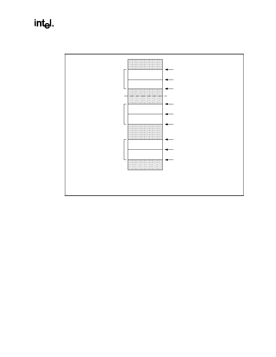
Intel
Æ
E8870SP Scalability Port Switch (SPS) Datasheet
4-3
Address Mapping
NOTE: The above discussion assumes A[43:40] are all 0's.
4.1.3
Routing Interrupts
Interrupts appear as Non-coherent writes with an attribute of INT. The destination of the
transaction is determined primarily by the method of interrupt delivery in the system.
SAPIC If the system is using the SAPIC method of interrupt delivery, then the interrupt will be
sent to the correct port using A[8:4] and the CBC register. A[8:4] of the SAPIC message contains
the NodeID.
Redirectable interrupts are indicated by A[3]. Logical/physical interrupts are indicated by
ReqTyp[0], and broadcast is indicated by A[19:12] = 0xFFh.
4.2
Address Mapping in I/O Space
The E8870 chipset allows I/O addresses to be mapped to resources supported on the I/O buses. The
SPS receives accesses to I/O space in the form of I/O reads and writes.
The SPS directs I/O accesses to the compatibility bridge, VGA space, or any valid I/O port (as
determined by the destination Attr bits). For I/O port accesses, the SPS uses the IOPORTS register
to determine which SIOH to send the access.
Figure 4-2. Example of Mapping MMIO Regions
001329
MMIO attribute set by SNC/SIOH if access
fails within one of these valid regions.
SIOH 1 (Port 2)
SIOH 0 (Port 5)
SIOH 1
SIOH 0
SIOH 0
High MMIO Region
SAPIC Range (SAR)
Low MMIO Region
4 GB Boundary
(1_0000_0000)
SIOH 1
Lower Bound in SNC/SIOH
MMIOLS
Upper Bound in SNC/SIOH
Lower Bound FEC0_0000
SARS
Upper Bound FECF_FFFF
Upper Bound in SNC/SIOH
MMIOHS
Lower Bound in SNC/SIOH

Address Mapping
4-4
Intel
Æ
E8870SP Scalability Port Switch (SPS) Datasheet
Table 4-2
shows the attribute encodings expected in this address space.
4.3
Address Mapping to Access Snoop Filter
The SF is not part of the address map. The address determines which of the four SFs on the SPS
will be used to process memory transactions. They are address interleaved. Using relatively low-
order address bits should result in evenly distributed accesses to all the SF interleaves.
SP responses to SPS requests need to access the SF to perform functions such as updating the final
cache line state.
4.4
Illegal Addresses
For most illegal accesses, the transaction is master aborted. Master abort has different specifics
depending on the initiating interface.
Table 4-2. I/O Space Mappings
I/O Address Space
Region
DEST ATTR
SPS Actions
Compat. Bus - Many
Regions
CB
Sends I/O reads and writes to correct SIOH as indicated by
CB_PORT register.
VGA
VGA
Sends I/O reads and writes to correct SIOH as indicated by
VGA_PORT register.
Other valid I/O port
DND
(Destination not
Decoded)
Sends I/O reads and writes to correct SIOH as indicated by
IOPORTS.
Config
DND
(Destination not
Decoded)
Decodes bus number and address to deliver configuration
access. If the configuration access is not to a component on the
chipset, sends configuration reads and writes to the correct
SIOH as indicated by the PSEG register.
Table 4-3. SPS Transactions to Illegal Addresses
Transactions
Description
Action
Coherent Memory
Accesses
The coherent memory access does not fall in
any MIR range, or the MIR is programmed to
route to an illegal port (6 or 7).
Send to the port identified by
MIR[0].WAY0.
SPS may generate a speculative
read, which is routed in the same
manner.
To an Unconnected Port
Any transaction to an unconnected SP port,
or illegal physical port ID in the crossbar.
Master abort.
To an Illegal Port
Illegal physical port ID in the crossbar, other
than when MIR is mis-programmed.
Route to Port 0.

Intel
Æ
E8870SP Scalability Port Switch (SPS) Datasheet
5-1
Functional Description
5
5.1
Interfaces
The SPS provides the glue logic to build multinode systems based on the SNC and SIOH
components. The primary interface of the SPS is the SP. The SPS also provides interfaces to
SMBus and JTAG.
5.1.1
Scalability Port
The SP is approximately 136 pins in width, with 40 bits of data used by the SP protocol. The SP
uses SBD signalling technology, which allows simultaneous transmission of information in both
directions on the same wire. It provides a peak bandwidth of 6.4 GB/s per port (3.2 GB/s in each
direction).
5.1.2
JTAG
The SPS supports the IEEE 1149.1 (JTAG) TAP for test and debug. The TAP interface is a serial
interface comprised of five signals: TDI, TDO, TMS, TCK, and TRST#. The JTAG interface will
operate from 0 to 25 MHz.
5.1.3
SMBus Interface
The SPS supports a SMBus 2.0 compatible slave interface to provide register visibility for a server
management subsystem. This low cost port is a two-pin (SDA, SCL) serial interface useful for
communicating with a baseboard management controller. The interface supports 100 kHz.
The interface allows for a multi-master subsystem, which means more than one device can initiate
data transfers at the same time. To support this feature, the SMBus bus arbitration relies on the
wired-AND connection of all SMBus interfaces. Two masters can drive the bus simultaneously
provided they are driving identical data. The first master drives SDA high, while another master
drives SDA low loses the arbitration. The SCL signal consists of a synchronized combination of
clocks generated by the masters using the wired-AND connection to the SCL signal.
The SMBus serial operation uses an open-drain wired-AND bus structure that allows multiple
devices to drive the bus lines and to communicate status about events such as arbitration, wait
states, error conditions and so on. For example, when the slave is unable to accept or drive data at
the rate that the master is requesting, the slave can hold the clock line low between the high states
to insert a wait interval. The master's clock can only be altered by a slower slave peripheral
keeping the clock line low or by another master during arbitration.
5.1.4
GPIO
There are two GPIO pins per SP for general purpose use. The value of these pins are observable
and controllable via the SPINCO register.
Functional Description
5-2
Intel
Æ
E8870SP Scalability Port Switch (SPS) Datasheet
5.2
Snoop Filter
The SF stores the tags and state information for all cache lines in the system. The SF is used to
determine whether a cache line associated with an address is cached in the system and where it is.
The coherency protocol engine or SPPC accesses the SF to look-up an entry, update/add an entry,
or invalidate an entry in the SF.
The SF has the following features:
∑
16K sets organized as a 12-way set-associative array.
∑
The sets are divided into four interleaves that can be accessed in parallel. Low order
interleaving based on 256-byte granularity.
∑
Support for 128-byte cache lines.
∑
Pseudo-Least-Recently-Used (PLRU) replacement algorithm, with updates on look-ups and
invalidates.
∑
Tag entries supporting a full 44-bit physical address space in a system. (43-bit addressing
when in a degraded mode.)
∑
Stores line state and presence vector (up to six nodes) for each valid cache line in the system.
∑
ECC coverage, with correction of single bit errors and detection of double bit errors.
∑
Fast-array initialization and/or self-test through configuration register access.
400 MHz operation that provides 66 MLUU/s per interleave (where a Look-up Update operation is
a read, followed by a write operation to the tag array). A maximum throughput of 266 MLUU/s per
SPS.
5.2.1
Coverage and Addressing
The SF is a 1 MB tag/data array that stores the state of all lines that are cached in the system (both
processor and SIOH).
Table 5-1
shows examples of the approximate SF coverage for certain
system configurations.
The tag array organization is 12-way set associative and is partitioned into four interleaves. Each
interleave can be accessed in parallel. Addressing of the interleaves is on a 256-byte granularity
(A[9:8]). This complements the 128-byte SP address interleaving by the SNC/SIOH (A[7]).
In a fully configured system, the SF supports a full 44-bit physical address. The size of the physical
address supported by the SF is reduced by one bit when the system is running in a degraded mode
using only one SPS.
Table 5-2
shows the partitioning of the address for different configuration options. Address
partitioning is determined by the following categories: SF interleave ID, and whether the system is
configured with a single SPS.
Table 5-1. Example SF Coverage for Different Node/L3 Configurations
Cache Line Size
Total Processors
L3 Cache Size (MB) per
Processor
Approximate SF
Coverage (per SPS)
128 Bytes
4
3
2X
128 Bytes
8
3
1X
128 Bytes
8
6
0.5X
Intel
Æ
E8870SP Scalability Port Switch (SPS) Datasheet
5-3
Functional Description
5.2.2
Replacement Algorithm
The SF implements a PLRU replacement algorithm using a vector of 12 bits for each set in the tag
array. The PLRU array requires 6 KB of storage per interleave. Each PLRU entry tracks the usage
of the 12 ways within a set, and is used to select a victim line in the event of a SF look-up that
results in a miss. The PLRU algorithm is implemented by factoring the number of ways into the
product of small integers 3*2*2. The minimum bit weight of this code is four (the number of
challenges before the entry can be promoted to LRU and selected as the next victim).
5.2.3
Snoop Filter Operations and Interfaces
Table 5-3
shows the organization of each SF entry and interpretation of the contents.
The SF supports the following operations:
∑
Look-up
On a look-up, the SF uses the tag and set portion of the input address to determine if the entry
is in the SF. The SF asserts a hit if there is a match and provides the contents, and way
information for the matched entry. If the look-up is a miss, the SF provides the contents of the
victim entry, set and way information of the victim. The PLRU vector is updated. The SF
indicates if a single or double bit error was detected. Single-bit errors are corrected (but the
array is not updated). Hit/miss calculation is performed after the ECC logic.
∑
Write
Set and way are provided for write operations. Writes can either be updates or invalidates. On
invalidations, the PLRU array is updated.
Table 5-2. Physical Address Partitioning
Configuration
Tag
Set
Interleave ID
SP Interleave
Cache Line
2 SPS
A[43:22]
A[21:10]
A[9:8]
A[7]
A[6:0]
1 SPS
A[42:21]
A[20:10,7]
A[9:8]
N/A
A[6:0]
Table 5-3. Snoop Filter Entry
Bits
Value
[35:29]
ECC check bits
[28]
State of the Cache Line:
1 - The cache line is in E/M state.
0 - The cache line is in S state.
[27:22]
Presence Vector:
[000000] The entry is invalid.
[xxxxxx] The entry is present in any of 6 nodes. Node0 is
the least significant bit. Node0 corresponds to physical
port 0 on the SPS.
[21:0]
Tag portion of the address.

Functional Description
5-4
Intel
Æ
E8870SP Scalability Port Switch (SPS) Datasheet
5.2.4
Error Correction and Logging
Each entry in the SF is protected by ECC. The SF reports a correctable error when:
∑
The look-up is a hit, and the entry has a single bit ECC error, or
∑
The look-up is a miss, and the victim entry has a single bit error.
An uncorrectable error is reported when:
∑
The look-up is a hit, and the entry has an uncorrectable error, or
∑
The look-up is a miss and any way within the set has an uncorrectable error.
If the look-up is a hit, any errors detected on other ways within the set are ignored. These errors
will be detected later when a miss occurs within the set.
5.2.5
Snoop Filter Performance
The SF tag array operates at 400 MHz. Reads/look-ups can be pipelined every two (400 MHz)
clocks, and writes every four (400 MHz) clocks. Each coherent request received from the SP
requires two SF operations, a LUU. Each SF interleave can support up to 66 MLUU/s, with a total
of 266 MLUU/s per SPS.
5.3
Interconnect
The SPS implements two methods for routing traffic between ports and interleaves: bypass buses
and a six-ported crossbar switch.
5.3.1
Bypass Buses
The following are the features of the bypass buses:
∑
Improves performance by "bypassing" the crossbar and decreasing latency. Used for low
latency snoop look-up and response connection between ports and interleaves. Also used for
issuing snoops to remote nodes.
∑
The bypass provides the only access from between a port and a SPPC.
∑
Each bus is shared between three ports and two interleaves, resulting in a total of four pairs of
bypass buses.
∑
Each bus has three requestors. The arbitration policy is pseudo round-robin, based on the SP
micro-interleaving scheme, channel availability, and other protocol-level buffer availability.
∑
Each bus can support 200 MT/s, providing 100 MA/s per interleave in a balanced system
configuration.
Together, the bypass buses can support a maximum of 800 MT/s from all ports in a balanced
system configuration. This is more than the maximum MLUU/s rate in all the SFs. The bypass
buses from a single port to the SPPCs can support a maximum of 400 MT/s to all the SPPCs,
assuming there is no activity from the other ports and evenly distributed traffic.

Intel
Æ
E8870SP Scalability Port Switch (SPS) Datasheet
5-5
Functional Description
5.3.2
Crossbar Switch
The following are the features of the crossbar switch:
∑
The crossbar has six ports and each port has two lanes. One lane is allocated for requests and
the other for responses.
∑
Flits are buffered in queues at the input to the crossbar. The queues are 16-flits deep.
∑
The arbitration algorithm used to transfer flits from the crossbar to the SPPD/SPPC port is
once-in-a-while interleaving, the same as the SP.
∑
Supports multiple packet sizes, using the tail flit to determine the end-of-packet.
∑
Packets are queued on the input side. Queue bypass is provided when the queue is empty to
improve idle latency.
∑
No bubbles inserted into the data stream from any port due to arbitration overhead/latencies. A
bubble has one or more cycles where data is not transferred from the crossbar to the port.
Packets with invalid port IDs are transferred to a default SPPD. The SPPD logs and reports the
error as an "Invalid Address" error.

Functional Description
5-6
Intel
Æ
E8870SP Scalability Port Switch (SPS) Datasheet

Intel
Æ
E8870SP Scalability Port Switch (SPS) Datasheet
6-1
Clocking
6
6.1
SPS Reference Clock (SYSCLK)
The SPS must have the same 200 MHz differential system clock source as all other E8870 chipset-
based components. Clocks on all branches of this system clock tree distribution should not drift by
more than 1 ns with respect to other branches. There is no clock gearing in the SPS. As the input
frequency changes, the core and SP must scale in frequency.
The SPS SYSCLK input does not require a phase relationship to the SYSCLK at the input of the
SNC or SIOH.
6.2
Other Functional and Electrical Requirements
6.2.1
Spread Spectrum Support
Spread Spectrum Clocking (SSC) is a frequency modulation technique for EMI reduction. Instead
of maintaining a constant frequency, SSC modulates the clock frequency/period along a
predetermined path (i.e. the modulation profile), with a predetermined modulation frequency.
The SPS and the rest of the E8870 chipset support SSC. The frequency modulation used is 30 kHz
with a downspread of 0.5%.
6.2.2
No Stop Clock or Thermal Shutdown
Clocks in the SPS cannot be stopped. There are no power reduction features in the SPS.
6.2.3
SMBus Clocking
Logic circuits exist in the SPS to accommodate metastability and synchronization of the serial
clock line (SCL) and the serial data line (SDA) to the SPS core clocks for processing serial data
streams. Also included is a 4-bit counter to suppress glitches less than 60 ns in width.
6.2.4
JTAG Test Access Port
Logic circuits exist in the JTAG unit to accommodate metastability and synchronization of TCK to
SPS core clocks for private instructions. Two synchronizers are used to provide rising and falling
edge detection of the JTAG clock.

Clocking
6-2
Intel
Æ
E8870SP Scalability Port Switch (SPS) Datasheet

Intel
Æ
E8870SP Scalability Port Switch (SPS) Datasheet
7-1
Reliability, Availability and
Serviceability
7
This chapter describes some general Reliability, Availability and Serviceability (RAS) concepts
that are applicable to the SPS component of the E8870 chipset.
7.1
Data Integrity
Errors are classified into two basic types: fatal (or non-recoverable) and non-fatal (or
recoverable).
1
Fatal errors include protocol errors, parity errors on header fields, time-outs, and
failed link-level retry. Fatal errors may compromise continued operation of the chipset.
E8870 chipset operations can continue with non-fatal errors (transactions are completed, resources
de-allocated, etc.). Non-fatal errors are categorized into correctable and non-correctable errors.
Non-correctable errors are those that are not "corrected" by the chipset. Non-correctable errors
may or may not be correctable by software. Correctable errors include single-bit ECC errors,
successful link level retry, and transactions where the chipset performs a master abort of the
transaction.
Each component in the chipset indicates an error condition on external pins. A pin (open drain) is
provided for each error type: fatal, uncorrectable, and correctable. It is up to the system to decide
the best course of action upon detecting an error.
Each E8870 chipset component provides error logging and error status for the first error detected
by the component and error status for subsequent errors. Errors are detected and logged at
intermediate entry points (on the inbound SP interface, for example). Errors are also detected at the
end points where the packet is consumed or translated to another interface with different error
coverage/detection. The end-point is where the error is corrected or the data is poisoned for data
errors.
2
This method of error detection, correction and error logging is called end-to-end error
correction.
The data that is logged and the name of the error log is also listed. Some errors may be detected in
more than one component, as is the case for many of the SP related errors.
7.1.1
End-to-End Error Detection
ECC errors are passed along to the end point. If the data path does not have ECC all the way,
single-bit errors are corrected just before the first ECC-less interface. Intermediate interfaces do
not correct single-bit ECC errors. The ECC check bits are always passed along with data internally.
A typical error leaves a trail behind in each component it passes. The system can use this to pin-
point the source of errors and to recover from error conditions.
1.
These are hardware definitions used by the E8870 chipset, and are not the same error types used by software (MCA).
2.
ECC data is poisoned by flipping ECC check bits 7:1, which will result in a syndrome value of 11111110. Parity data is poisoned by flipping
all of the parity bits associated with the data. Memory Device Failure Recovery ECC is poisoned by inverting symbols a and b.

Reliability, Availability and Serviceability
7-2
Intel
Æ
E8870SP Scalability Port Switch (SPS) Datasheet
The SPS has the following end points for data:
Configuration Registers
∑
On write, convert to internal configuration cycles if no error is detected by ECC.
∑
On write, convert to internal configuration cycles after single-bit ECC errors are corrected.
∑
On write, the write is not performed and a normal response is returned if an uncorrectable ECC
error is detected.
∑
On read, generate good ECC.
7.1.2
Error Reporting
7.1.2.1
Error Status and Log Registers
Two types of error status registers are provided: first error status register (FERRST[1:0]) and
second, or subsequent, error status register (SERRST[1:0]). The first fatal and/or first non-fatal
errors are flagged in the FERRST register; subsequent errors are indicated in the SERRST. Use of
the FERRST[1] and SERRST[1] registers is not supported and should not be used.
Control and data logs are associated with some of the errors flagged in the FERRST register. In
some cases, the logs are duplicated for the same error (for example, two Hub Interfaces on the
SIOH may have the same error log registers). When error logs are duplicated, a pointer is provided
to the cluster that reported the first error.
The contents of FERRST and SERRST are "sticky" across a reset (while PWRGOOD remains
asserted). This allows firmware to perform diagnostics across reboots.
7.1.2.2
Error Signaling
Three open drain error pins are associated with each pair of FERRST/SERRST registers, one for
each error type: fatal, uncorrectable and correctable. (ERRD0[2:0]#, ERRD1[2:0]#, respectively).
If not masked (ERRMSK[1:0] register), these pins reflect the error status of each type in the two
error status registers.
The value of the error pins, when an error is flagged, is also stored in the FERRST to facilitate the
identification of the first error in the system. When a first fatal error is detected on the component,
for example, the value of the error status pin associated with fatal errors is also latched into the
FERRST.
The error pins are asynchronous I/O signals. To filter glitches on the inputs, the value of the signal
only changes when the same value has been sampled over four consecutive cycles (200 MHz
system clock). To ensure accurate sampling of these signals by other devices on the output, the
output value is asserted for a minimum of six consecutive clock cycles (200 MHz system clock).
For reliable signaling of errors in the system, each component guarantees that the pin associated
with the error is asserted within four system clock cycles (200 MHz) after the error is detected by
the component. For example, if a multi-bit ECC error is detected at the SP interface in cycle x, the
uncorrectable error pin (ERRDx[1]) is asserted in cycle x+3.

Intel
Æ
E8870SP Scalability Port Switch (SPS) Datasheet
7-3
Reliability, Availability and Serviceability
7.1.2.3
Error Logs
Control and/or data logs are provided for some errors. The "non-recoverable" error logs are used to
log information associated with first fatal errors. The "recoverable" error logs are used for first
non-fatal errors.
Once a first error for a type of error has been flagged (and logged), the log registers for that error
type remain fixed until either:
∑
All bits associated with the error type in the FERRST are cleared, or
∑
A power-up reset.
More specifically, when the status bits associated with fatal errors are cleared in FERRST, updates
to the non-recoverable error logs are enabled. When the status bits associated with non-fatal errors
are cleared in FERRST, updates to the recoverable error logs are enabled.
7.1.3
Interface Details
Major interfaces in the chipset can be enabled/disabled via software to aid fault isolation. Any
requests routed to a disabled interface are master-aborted. Any responses are absorbed. That is, no
issue is required on the disabled interface, but the disabled interface must not assert internal flow
control.
Scalability Port
∑
Data is protected by ECC. ECC is checked only on entry of packets.
∑
Flits transfers are protected by parity.
∑
The information contained in the SP control and idle flits packet are protected by both parity
and duplication (each field is duplicated on different wires to enhance error detection).
∑
Link level retry is supported on the SP. Link level retry is entered when parity errors are
detected on flits, or when phits within an idle flit have a duplication error.
∑
SPS's SFs are protected by ECC.
Configuration Registers
∑
ECC is checked on configuration writes.
SMBus
∑
The SMBus port supports the optional Packet Error Correction feature of the SMBus
Specification, Revision 2.0. This feature allows the slave to append an 8-bit CRC to read
completions.
7.1.4
Time-out
Certain transactions of the SPS SPPC cluster are tracked by timer(s). A time-out transaction is
logged in the error registers as a fatal error. The time-out transaction does not need to be cleaned or
removed.
When an entry in the queue is allocated, it becomes valid and is tracked by the master timer logic.
The timer is a 24-bit wrap-around counter, incrementing at 25 MHz (200 MHz core clock divided
by 8). This provides a maximum time-out period of approximately 640 ms. The actual time-out
period is programmable (a value in the ERRCOM register that determines the size of the counter).

Reliability, Availability and Serviceability
7-4
Intel
Æ
E8870SP Scalability Port Switch (SPS) Datasheet
The timer interval must be greater than the worst-case latency required in the system to de-allocate
the queue entry. For example, the interval must be set to greater than the worst-case latency from
the SP issue to the response, including contention scenarios for all resources the request must
acquire.
An entry times out if the counter wraps around (toggles the high-order) bit twice. As a result, the
time-out period can be from 1x to 2x the timer value.
Using such a mechanism, it is possible for multiple entries in a queue to time-out simultaneously.
When a time-out occurs, the hardware selects one entry as the "first error" for logging in the
FERRST. The presence of more than one error is indicated in the SERRST register.
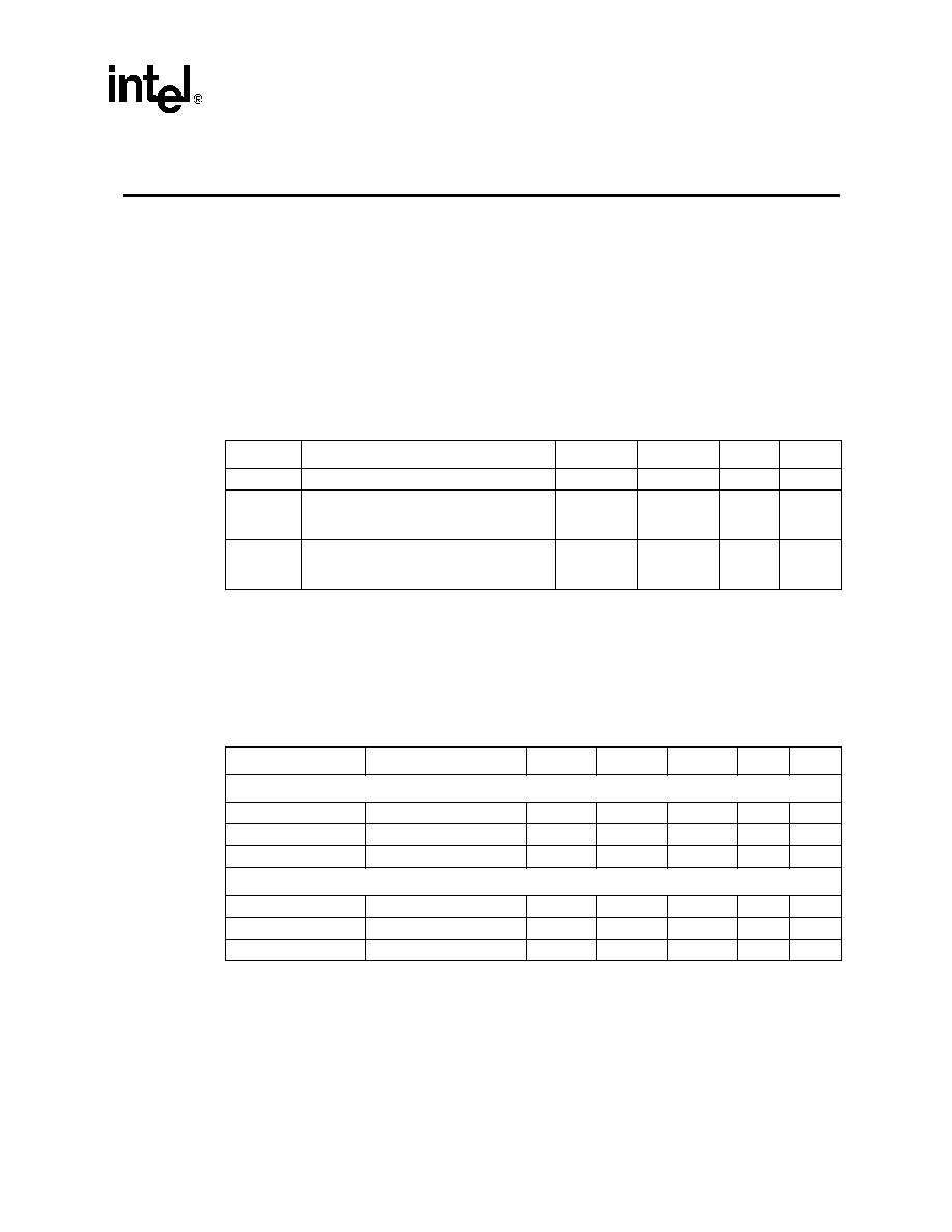
Intel
Æ
E8870SP Scalability Port Switch (SPS) Datasheet
8-1
Electrical Specification
8
8.1
Non-operational Maximum Rating
The absolute maximum non-operational DC ratings are provided in
Table 8-1
. Functional operation
at the absolute maximum and minimum ratings is neither implied nor guaranteed. The SPS should
not receive a clock while subjected to these conditions. Functional operating conditions are given
in the AC and operational DC tables. Furthermore, although the SPS contains protective circuitry
to resist damage from static discharge, one should always take precautions to avoid high static
voltages or electric fields.
8.2
Operational Power Delivery Specification
SPS power requirements are outlined in this section. All parameters in
Table 8-2
are specified at
the pin
of the component package.
Table 8-1. Absolute Maximum Non-operational DC Ratings at the Package Pin
Symbol
Parameter
Minimum
Maximum
Unit
Notes
Tstorage
SPS Chipset Storage Temperature
≠10
45
∞C
Vcc (All)
SPS Supply Voltage with Respect to Vss
≠0.50
Operating
voltage +
0.50
V
Vcc
(CMOS)
CMOS Buffer DC Input Voltage with
Respect to Vss
≠0.50
Vcc
(CMOS) +
0.50
V
Table 8-2. Voltage and Current Specifications
Symbol
Parameter
Minimum
Typical
Maximum
Unit
Notes
Core Voltage and I/O
Vcc Core
Voltage
1.425
1.5
1.575
V
a
a. Specification comprehends all AC and DC components.
ICC
CORE
Core Current
22
A
b
b. The maximum ICC current is the worst case specification, (i.e. Vcc max, low temperature and application mix) intended for
power supply design.
dICC/dt
(Core)
Transient Core Slew Rate
6
A/ns
Scalability Port Interface
c
c. Estimated values provided for power budgeting considerations; these parameters are not tested. This is the same SP interface
as specified in SIOH and SNC.
VCCSP
SP Supply Voltage
1.209
1.30
1.391
V
d, e, f
d. VCCSP budget is ±3% DC, and (DC + AC) at ±7% noise delivered at the pin.
e. The power pins are separated at the package from the Vcc core or other supplies on-die.
f. The power supply must be local to each component. The SP power supply between two communicating ports needs to be
separate.
Isp
SP Current
0.50
A
g, h
g. The current requirement per SP port.
h. Under normal operating conditions. However, under certain test conditions, Isp might exceed the specification.
dIsp/dt
Transient Slew Rate
1.0
A/ns
i
i. The specification is per SP port at the package pin.
Electrical Specification
8-2
Intel
Æ
E8870SP Scalability Port Switch (SPS) Datasheet
8.3
Scalability Port Signal Group
The SP interface is a source-synchronous interface with coincident data and continuous strobe
transmission. The data and strobe signals are launched simultaneously and are expected to arrive at
the receiver with the same timing relationship to one another.
Each SP port consists of two strands that are further subdivided into two bundles. Each SP port
consists of 32 data bits, four ECC bits, two parity bits, two SSO coding bits, two link layer control
(LLC) bits, four strobe pairs (eight signal pins), reserved pins, and eight reference voltage pairs
(sixteen signal pins).
The SBD signaling can create conditions for three logic levels on the interconnect (0, 0.65, 1.3)V,
depending on the data values driven from each end of the trace.
All SBD signals are terminated via on-die termination. The reference voltages are generated on die
and are set to 1/4 VCCSP and 3/4 VCCSP, so no external logic is needed to generate these
reference voltages.
Each SP voltage reference pin is required to be interlinked to the corresponding SP port.
Table 8-3
summarizes the signal grouping of the SP interface. The "x" in the signal names is
replaced with the SP port numbers 0≠5.
8.4
SMBus and TAP Electrical Specifications
The SPS uses open-drain outputs and has its own defined logic levels, which are different than
CMOS logic levels. The signals that are used are listed in
Table 8-4
.
The TAP connection input signals require external termination (see
Table 8-5
). No reference
voltage is required for these signals.
The SMBus and TAP signals require termination to 3.3V and 1.5V on the motherboard,
respectively.
Table 8-3. Scalability Port Interface Signal Group
Signal Group
Signal
SBD I/O
SPxAD[15;0],SPxBD[15;0], SPxASTBP[1:0], SPxBSTBP[1:0],
SPxASTBN[1:0], SPxBSTBN[1:0], SPxAEP[2:0], SPxBEP[2:0], SPxALLC,
SPxBLLC, SPxASSO, SPxBSSO
CMOS1.5 I/O OD
SPxGPIO[1:0]
CMOS1.3 INPUT
a
a. See Section
Section 8.7.1
for "CMOS 1.3" specifications.
SPxPRES
CMOS1.3 I/O
SPxSYNC
Power/Other
VCCSP
b
, VSS
b. Vccsp is to be supplied to the SP port externally. See
Table 8-2
.
Analog I/O
c
c. VrefH and VrefL are generated on-die.
SPxZUPD[1:0]
d
, SPxAVREFH[3:0], SPxBVREFH[3:0], SPxAVREFL[3:0],
SPxBVREFL[3:0]
d. SPxZUPD0 impedance update pins are connected through 45 ohm 1% resistor to Vccsp; SPxZUPD1 impedance update pins
are connected through 45 ohm 1% resistor to Vss.
SP Analog Input
VCCA
e
, VSSA
e. PLL analog voltage for SP, connected on the motherboard to 1.5V nominal ±5% supply through a filter network.
Intel
Æ
E8870SP Scalability Port Switch (SPS) Datasheet
8-3
Electrical Specification
For specifications related to components or external tools that will interface with the SPS, refer to
that component or tool's associated specification.
8.5
DC Specifications
Table 8-4. SMBus and TAP Interface Signal Group
Signal Group
Signal
SMBus
(I/O)
SCL, SDA
TAP
(Input)
TCK, TDI, TMS, TRST#
TAP
(Output)
TDO
Table 8-5. TAP Signal Terminations
a, b
a. Termination values for input pins are based on requirements
of Intel's in-target probe. Requirements for other applications
may differ.
b. All resistances are nominal with a tolerance allowance of
±
5%.
TCK
27 ohm to GND
TMS
39 ohm to VCC
TDI
c
c. This TDI pull-up value applies only to TDI inputs driven by
Intel's in-target probe TAP controller.
150 ohm to VCC
TDO, TDI
75 ohm to VCC
TRST#
500-680 ohm to GND
Table 8-6. TAP DC Parameters
a
a. All specifications are at the pin of the package.
Symbol
Parameter
Minimum
Maximum
Unit
Notes
V
IL
Input Low Voltage
-0.4
0.76
V
V
IH
Input High Voltage
1.16
1.8
V
V
T
-
Negative-going Threshold Voltage
0.76
1.03
V
b
b. See
Figure 8-1
.
V
T
+
Positive-going Threshold Voltage
0.91
1.16
V
b
V
H
Hysteresis
Voltage
130
mV
b
V
oL
Output Low Voltage
0.34
0.49
V
c
c. Measured with a 75 ohm
±
10% test load to Vcc.
I
li
Input Leakage Current
10
µA
c
I
ol
Output Low Current
12.7
mA
c
Electrical Specification
8-4
Intel
Æ
E8870SP Scalability Port Switch (SPS) Datasheet
8.6
AC Specifications
Figure 8-1. TAP DC Thresholds
Table 8-7. SMBus DC Parameters
a, b
a. All specifications are at the pin of the package.
b. Parameters apply to SMBus inputs, output, and I/O buffers.
Symbol
Parameter
Minimum
Maximum
Unit
Notes
V
IL
Input Low Voltage
≠0.5
0.8
V
V
IH
Input High Voltage
2.1
3.47
V
V
oL
Output Low Voltage
0.4
V
c
c. At Vol max, Iol = 4 mA.
I
li
Input Leakage Current
50
µA
I
pullup
Current through Pull-up Resistor
4.0
mA
C
in
Input Capacitance
10
pF
V
noise
Signal Noise Immunity
300
mV
d, e
d. At 1 MHz to 5 MHz range.
e. Peak to peak.
Table 8-8. SMBus Signal Group AC Specifications
a
a. All AC timings for the SMBus signals are referenced to the SM_CLK signal at 0.5 ∑ SM_VCC at the package pins. All SMBus
signal timings (SM_DAT, SM_ALERT#, etc.) are referenced at 0.5 ∑ SM_VCC at the package pins.
Symbol
Parameter
Minimum
Maximum
Unit
Figure
Notes
f
smb
Operating
Frequency
10
100
kHz
T60
SMBus Output Valid Delay
1.0
us
8-2
T61
SMBus Input Setup Time
250
ns
8-2
T62
SMBus Input Hold Time
300
ns
8-2
T
r
Clock/Data Rise Time
1000
ns
b
b. T
r
= (V
il,max
-0.15) to (V
ih,min
+0.15).
T
f
Clock/Data Fall Time
300
ns
c
c. T
f
= (V
ih,min
+0.15) to (V
il,max
-0.15).
T
bf
Bus Free Time
4.70
µ
s
d
d. Minimum time allowed between request cycles.
TAP
Signal
V
T
+
(max)
V
T
+
(min)
V
T
-
(max)
V
T
-
(min)
V
H (min)
V
H (min)
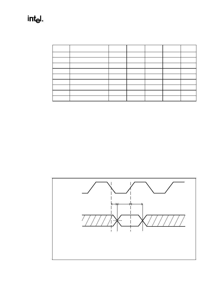
Intel
Æ
E8870SP Scalability Port Switch (SPS) Datasheet
8-5
Electrical Specification
8.6.1
AC Timing Waveforms
Figure 8-2
and
Figure 8-3
are used in conjunction with the AC timing
Table 8-4
and
Table 8-5
.
Note:
The following apply:
1. All AC timings for the TAP signals are referenced to the TCK signal at 0.5 ∑ Vcc_tap at the
component pin. All TAP signal timings (TMS, TDI, etc.) are referenced at the package pin.
2. All AC timings for the SMBus signals are referenced to the SM_CLK signal at 0.5 ∑ SM_Vcc
at the component pin. All SMBus signal timings (SM_DAT, SM_ALERT#, etc.) are
referenced at 0.5 ∑ SM_Vcc at the package pin.
Table 8-9. TAP Signal Group AC Specifications
a
a. All AC timings for the TAP signals are referenced to TCK at 50% voltage level.
Symbol
Parameter
Minimum
Maximum
Unit
Figure
Notes
T
ck
TCK Frequency
1.0
20
MHz
8-3
T58
TCK, TMS, TDI Rise Time
0.5
16
ns
8-3
b
b. Rise and fall times are measured from the 20% to 80% points of the signal swing.
T59
TCK, TMS, TDI Fall Time
0.5
16
ns
b
T
r
TDO Rise Time
2.3
4.6
ns
b
T
f
TDO Fall Time
1.2
5.3
ns
b
T60
TDO Clock to Output Delay
2.5
10
ns
8-2
c
c. Referenced to the falling edge of TCK.
T61
TDI, TMS Setup Time
5
ns
8-2
d,
e
d. Specification for a minimum swing defined between TAP V IL_MAX to V IH_MIN. This assumes a minimum edge rate of
0.5V per ns.
e. Referenced to the rising edge of TCK at the component pin.
T62
TDI, TMS Hold Time
18
ns
8-2
d, e
TRST#
Assert Time
300
ns
Figure 8-2. TAP and SMBus Valid Delay Timing Waveform
T
x
= T60 (Valid Time)
T
s
= T61 (Setup Time)
T
h
= T62 (Hold Time)
V = 0.5 * SM_Vcc for SMBus Signal Group
Clock
Signal
T
x
T
s
T
h
Valid
V

Electrical Specification
8-6
Intel
Æ
E8870SP Scalability Port Switch (SPS) Datasheet
8.7
Miscellaneous Signal Pins
All buffer types that do not belong to one of the major buses in the system are listed as
miscellaneous signals.
8.7.1
Signal Groups
Figure 8-3. TCK and SM_CLK Clock Waveform
T
r
= T58, T74 (Rise Time)
T
f
= T59, T75 (Fall Time)
T
h
= T72 (High Time)
T
l
= T73 (Low Time)
T
p
= T55 (TCK, SM_CLK Period)
V
1
, V
2
: For rise and fall times, TCK and SM_CLK are measured between 20% and 80% points.
Clock
T
h
* V
1
* V
2
T
r
T
p
T
l
T
f
Clock
T
h
* V
1
* V
2
T
r
T
p
T
l
T
f
Table 8-10. Signal Groups
Signal Group
Signal
CMOS1.3 Input
SPxPRES
CMOS1.3 I/O
SPxSYNC
CMOS1.5 I/O OD
EV[3:0]#, ERRD0[2:0]#,ERRD1[2:0]#, SPxGPIO[1:0]
CMOS1.5 O OD
INT_OUT[1:0]#
CMOS1.5 Input
BPIN, LVHSTLODTEN, NODEID[4:0], PWRGOOD, RESETI#
a
,
RESETID[1:0]#
a. Requires external 330 ohm pull-up resistor.
CMOS1.5 Output
BPOUT
ANALOG INPUT VCC
VCCACORE
b
, VSSACORE
b. PLL analog voltage input for core PLL, connect to 1.5V ±5% through a network filter.
Intel
Æ
E8870SP Scalability Port Switch (SPS) Datasheet
8-7
Electrical Specification
8.7.2
DC Characteristics
Table 8-11. CMOS 1.3V DC Parameters
a, b
a. All specifications are at the pin of the package.
b. Parameters apply to all CMOS 1.3V buffer types unless otherwise noted.
Symbol
Parameter
Minimum
Maximum
Unit
Notes
V
IL
Input Low Voltage
≠0.3
0.35
V
V
IH
Input High Voltage
1.11
VCCSP
+0.3
V
V
oL
Output Low Voltage
≠0.15
0.26
V
c
c. Not applicable for CMOS 1.3V input buffer types.
V
oH
Output High Voltage
1.21
1.39
V
c
I
li
Input Leakage Current
10
µA
R
on
On-Resistance
41.4
45.5
ohm
Table 8-12. CMOS 1.5V OD DC Parameters
a
a. Supply voltage at 1.5V ±5% tolerance.
Symbol
Parameter
Minimum
Maximum
Unit
Notes
V
IH
Input High Voltage
1.15
Vcc +0.3
V
V
IL
Input Low Voltage
≠0.3
0.70
V
V
oH
Output High Voltage
1.3
Vcc +0.3
V
b
b. RI = 50 or 25 ohms.
V
oL
Output Low Voltage
0.54
V
c
c. RI = 25 ohms.
I
ol
Output Low Current
52.0
mA
c
I
li
Input Leakage Current
50
µA
Table 8-13. CMOS 1.5V DC Parameters
a
a. Supply voltage at 1.5V ±5% tolerance.
Symbol
Parameter
Minimum
Maximum
Unit
Notes
V
IH
Input High Voltage
0.90
Vcc +0.3
V
V
IL
Input Low Voltage
≠0.30
0.70
V
V
oH
Output
High
Voltage
0.8
∑ Vcc
VCC +0.3
V
V
oL
Output Low Voltage
0.20 ∑ VCC
V
V
hysteresis
Hysteresis
Voltage
0.10
V
Ron
Output Impedance
30
80
ohm
I
li
Input Leakage Current
70
µA
Electrical Specification
8-8
Intel
Æ
E8870SP Scalability Port Switch (SPS) Datasheet
8.8
AC Specification
Table 8-14. CMOS 1.3V AC Parameters
a
a. Clock delay is in reference to the 200 MHz clock.
Symbol
Parameter
Minimum
Maximum
Unit
Notes
Tco
Clock to Output Valid Delay
0.15
15.0
ns
SRf
Output Slew Rate Fall
0.25
0.7
V/ns
SRr
Output Slew Rate Rise
0.5
15.0
V/ns
Table 8-15. CMOS 1.5V Open-Drain AC Parameters
a, b
a. Supply voltage at 1.5V ±5% tolerance.
b. Clock delay is in reference to the 200 MHz clock.
Symbol
Parameter
Min
Max
Unit
Notes
Signals: INT_OUT[1:0]#
Tco
Clock to Output Valid Delay
6.0
ns
c
c. RI = 25-ohms.
SRf
Output Slew Rate Fall
0.25
0.91
V/ns
c
SRr
Output Slew Rate Rise
0.37
1.18
V/ns
c
Signals: EV[3:0], ERRD0[2:0], ERRD1[2:0]
Tco
Clock to Output Valid Delay
1.5
6.0
ns
Tsu
Input Setup Time
1
ns
Thold
Input Hold Time
ns
d
d. Input must be sampled at the same value 4 consecutive cycles before changing state.
SRf
Output Slew Rate Fall
0.25
0.91
V/ns
SRr
Output Slew Rate Rise
0.37
1.18
V/ns
Signal: SPxGPIO[1:0]
Tco
Clock to Output Valid Delay
6.0
ns
Tsu
Input Setup Time
1
ns
Thold
Input Hold Time
ns
d
SRf
Output Slew Rate Fall
0.25
0.91
V/ns
SRr
Output Slew Rate Rise
0.37
1.18
V/ns
Table 8-16. CMOS 1.5V AC Parameters
a, b
a. Supply voltage at 1.5v ±5% tolerance.
b. Clock delay is in reference to the 200 MHz clock.
Symbol
Parameter
Minimum
Maximum
Unit
Notes
Tco
Clock to Output Valid Delay
≠0.28
1.44
ns
Tsu
Input Setup Time
0.84
ns
Thold
Input Hold Time
0.35
ns
SRf
Output Slew Rate Fall
2.00
5.00
V/ns
SRr
Output Slew Rate Rise
1.90
4.9
V/ns
Intel
Æ
E8870SP Scalability Port Switch (SPS) Datasheet
8-9
Electrical Specification
8.9
Intel
Æ
E8870 Chipset Clock Signal Groups
Table 8-17. Clock Signal Groups
Signal Group
Signals
LVHSTL Differential Inputs
SYSCLK,SYSCLK#
Table 8-18. LVHSTL Clock DC Parameters
Symbol
Parameter
Minimum
Typ
Maximum
Unit
V
IH
Input High Voltage
0.78
1.3
V
V
IL
Input Low Voltage
≠0.3
0.5
V
V
X
Input Crossover Voltage
0.55
0.85
V
C
CLK
Input
Capacitance
1.0
11.5
pF

Electrical Specification
8-10
Intel
Æ
E8870SP Scalability Port Switch (SPS) Datasheet

Intel
Æ
E8870SP Scalability Port Switch (SPS) Datasheet
9-1
Ballout and Package Information
9
9.1
1012-Ball OLGA2b Package Information
The 1012-ball OLGA2b package of the SPS has an exposed die mounted on a package substrate.
The package's coplanarity has a mean of approximately 8-mils and a tolerance at 4-sigma of
approximately 4-mils. A heatsink, with appropriate interface material and retention capabilities, is
required for proper operation (refer to
Figure 9-1
and
Figure 9-2
).
Figure 9-1. 1012-Ball OLGA2b Package Dimensions ≠ Top View
001328
42.50 mm
28.50 mm
32.50 mm
32.50 mm 42.50 mm
Handling Exclusion Area
SPS
Die
28.50 mm
Die Keepout Area
0.744 in.
1.044 in.
0.757 in.
0.957 in.
0.100 in.
0.100 in.
0.100 in.
0.200 in.

Ballout and Package Information
9-2
Intel
Æ
E8870SP Scalability Port Switch (SPS) Datasheet
Figure 9-2. 1012-Ball OLGA2b Package Dimensions ≠ Bottom View
001250
C
A
B
D
F
E
G
14
12
11
13
10
27
21
19
18
20
15 16 17
25
24
26
22 23
32
31
28 29 30
AB
N
H
K
J
L
M
P
Y
T
R
U
W
V
AA
AF
AE
AD
AC
AH
AK
AJ
AG
AL
AM
1
4 5
7
6
2 3
8 9
2 x 42.500 ±0.100
1.270
19.685
39.370
0.200 A B
-B-
2 x 1.465 Min.
-A-
21.250
1.270
0.635

Intel
Æ
E8870SP Scalability Port Switch (SPS) Datasheet
9-3
Ballout and Package Information
Figure 9-3. 1012-Ball OLGA2b Solder Ball Detail
001248
Die
J
OLGA Substrate
2.140 ±0.150
H
1.300 ±0.100
0.600 ±0.100
BGA Solder
Balls
0.74 ±0.025
0.100 ±0.025
Die Solder
Bumps
Underfill
Epoxy
Detail H
Detail J

Ballout and Package Information
9-4
Intel
Æ
E8870SP Scalability Port Switch (SPS) Datasheet
Table 9-1. SPS Ball List
Ball Number
Signal
Ball Number
Signal
A3
SP0BVREFL[1]
B12
SP0ASTBP[0]
A4
VCCSP
B13
VSS
A5
SP0BD[2]
B14
SP0AEP[0]
A6
VSS
B15
VSS
A7
SP0BD[1]
B16
SP0AD[5]
A8
VSS
B17
SP1BD[5]
A9
SP0BD[0]
B18
VSS
A10
VSS
B19
SP1BEP[0]
A11
SP0AEP[2]
B20
VSS
A12
VSS
B21
SP1BSTBP[0]
A13
SP0AD[2]
B22
VSS
A14
VSS
B23
SP1BD[0]
A15
SP0AD[4]
B24
VSS
A16
VCCSP
B25
SP1AVREFL[0]
A17
VCCSP
B26
VSS
A18
SP1BD[4]
B27
SP1ASTBN[0]
A19
VSS
B28
VSS
A20
SP1BD[2]
B29
SP1AVREFH[1]
A21
VSS
B30
VSS
A22
SP1BEP[2]
B31
SP1AD[6]
A23
VSS
C1
SP0BD[5]
A24
SP1AD[0]
C2
VCCSP
A25
VSS
C3
SP0BD[4]
A26
SP1AD[1]
C4
VSS
A27
VSS
C5
SP0BD[3]
A28
SP1AD[2]
C6
VCCSP
A29
VCCSP
C7
SP0BSTBP[0]
A30
SP1AVREFL[1]
C8
VSS
B2
SP0BD[6]
C9
SP0BVREFH[0]
B3
VSS
C10
VCCSP
B4
SP0BVREFH[1]
C11
SP0AD[1]
B5
VSS
C12
VSS
B6
SP0BSTBN[0]
C13
SP0AD[3]
B7
VSS
C14
VCCSP
B8
SP0BVREFL[0]
C15
SP0AD[7]
B9
VSS
C16
VSS
B10
SP0AD[0]
C17
VSS
B11
VSS
C18
SP1BD[7]
Intel
Æ
E8870SP Scalability Port Switch (SPS) Datasheet
9-5
Ballout and Package Information
C19
VCCSP
D26
VSS
C20
SP1BD[3]
D27
SP1AEP[1]
C21
VSS
D28
VSS
C22
SP1BD[1]
D29
SP1AEP[0]
C23
VCCSP
D30
VSS
C24
SP1AVREFH[0]
D31
SP1AD[7]
C25
VSS
D32
VSS
C26
SP1ASTBP[0]
E1
SP0BD[15]
C27
VCCSP
E2
VSS
C28
SP1AD[3]
E3
SP0BSSO
C29
VSS
E4
VCCSP
C30
SP1AD[4]
E5
SP0BRSVD
C31
VCCSP
E6
VSS
C32
SP1AD[5]
E7
SP0BLLC
D1
VSS
E8
VCCSP
D2
SP0BD[7]
E9
SP0AVREFH[2]
D3
VSS
E10
VSS
D4
SP0BEP[0]
E11
SP0AVREFL[0]
D5
VSS
E12
VCCSP
D6
SP0BEP[1]
E13
SP0AEP[1]
D7
VSS
E14
VSS
D8
SP0BEP[2]
E15
SP0AVREFL[1]
D9
VSS
E16
VCCSP
D10
SP0AVREFH[0]
E17
VCCSP
D11
VSS
E18
SP1BVREFL[1]
D12
SP0ASTBN[0]
E19
VSS
D13
VSS
E20
SP1BEP[1]
D14
SP0AVREFH[1]
E21
VCCSP
D15
VSS
E22
SP1BVREFL[0]
D16
SP0AD[6]
E23
VSS
D17
SP1BD[6]
E24
SP1BVREFH[2]
D18
VSS
E25
VCCSP
D19
SP1BVREFH[1]
E26
SP1ALLC
D20
VSS
E27
VSS
D21
SP1BSTBN[0]
E28
SP1ARSVD
D22
VSS
E29
VCCSP
D23
SP1BVREFH[0]
E30
SP1ASSO
D24
VSS
E31
VSS
D25
SP1AEP[2]
E32
SP1AD[15]
Table 9-1. SPS Ball List (Continued)
Ball Number
Signal
Ball Number
Signal

Ballout and Package Information
9-6
Intel
Æ
E8870SP Scalability Port Switch (SPS) Datasheet
F1
VSS
G8
VSS
F2
SP0BD[12]
G9
SP0AVREFL[2]
F3
VSS
G10
VCCSP
F4
SP0BD[11]
G11
SP0ASTBN[1]
F5
VSS
G12
VSS
F6
SP0BSTBP[1]
G13
SP0ASSO
F7
VSS
G14
VCCSP
F8
SP0BVREFL[2]
G15
SP0AD[15]
F9
VSS
G16
VSS
F10
SP0AD[9]
G17
VSS
F11
VSS
G18
SP1BD[15]
F12
SP0AD[10]
G19
VCCSP
F13
VSS
G20
SP1BSSO
F14
SP0AVREFL[3]
G21
VSS
F15
VSS
G22
SP1BSTBN[1]
F16
SP0AD[14]
G23
VCCSP
F17
SP1BD[14]
G24
SP1BVREFL[2]
F18
VSS
G25
VSS
F19
SP1BVREFL[3]
G26
SP1AVREFH[2]
F20
VSS
G27
VCCSP
F21
SP1BD[10]
G28
SP1ASTBN[1]
F22
VSS
G29
VSS
F23
SP1BD[9]
G30
SP1AVREFH[3]
F24
VSS
G31
VCCSP
F25
SP1AVREFL[2]
G32
SP1AD[13]
F26
VSS
H1
VSS
F27
SP1ASTBP[1]
H2
SP0BVREFL[3]
F28
VSS
H3
VSS
F29
SP1AD[11]
H4
SP0BD[10]
F30
VSS
H5
VSS
F31
SP1AD[12]
H6
SP0BD[9]
F32
VSS
H7
VSS
G1
SP0BD[13]
H8
SP0BD[8]
G2
VCCSP
H9
VSS
G3
SP0BVREFH[3]
H10
SP0ALLC
G4
VSS
H11
VSS
G5
SP0BSTBN[1]
H12
SP0ARSVD
G6
VCCSP
H13
VSS
G7
SP0BVREFH[2]
H14
SP0AVREFH[3]
Table 9-1. SPS Ball List (Continued)
Ball Number
Signal
Ball Number
Signal

Intel
Æ
E8870SP Scalability Port Switch (SPS) Datasheet
9-7
Ballout and Package Information
H15
VSS
J22
SP1BSTBP[1]
H16
SP0AD[13]
J23
VSS
H17
SP1BD[13]
J24
SP1BD[8]
H18
VSS
J25
VCCSP
H19
SP1BVREFH[3]
J26
SP5BD[14]
H20
VSS
J27
VSS
H21
SP1BRSVD
J28
SP5BD[6]
H22
VSS
J29
VCCSP
H23
SP1BLLC
J30
SP5BD[5]
H24
VSS
J31
VSS
H25
SP1AD[8]
J32
SP1AD[14]
H26
VSS
K1
VSS
H27
SP1AD[9]
K2
SP4AD[7]
H28
VSS
K3
VSS
H29
SP1AD[10]
K4
SP4AD[4]
H30
VSS
K5
VSS
H31
SP1AVREFL[3]
K6
SP4AD[15]
H32
VSS
K7
VSS
J1
SP0BD[14]
K8
SP4AD[13]
J2
VSS
K9
VSS
J3
SP4AD[5]
K10
SP0ZUPD[0]
J4
VCCSP
K11
TMS
J5
SP4AD[6]
K12
SYSCLK#
J6
VSS
K13
VCC
J7
SP4AD[14]
K14
LVHSTLODTEN
J8
VCCSP
K15
VCC
J9
SP0AD[8]
K16
330 Ohm P/D
J10
VSS
K17
RESETID#[1]
J11
SP0ASTBP[1]
K18
VCC
J12
VSS
K19
TDIOCathode
J13
SP0AD[11]
K20
VCC
J14
VSS
K21
RSVD[1]
J15
SP0AD[12]
K22
TDIOAnode
J16
VCCSP
K23
SP1SYNC
J17
VCCSP
K24
VSS
J18
SP1BD[12]
K25
SP5BD[13]
J19
VSS
K26
VSS
J20
SP1BD[11]
K27
SP5BD[15]
J21
VSS
K28
VSS
Table 9-1. SPS Ball List (Continued)
Ball Number
Signal
Ball Number
Signal

Ballout and Package Information
9-8
Intel
Æ
E8870SP Scalability Port Switch (SPS) Datasheet
K29
SP5BD[4]
M4
SP4AD[3]
K30
VSS
M5
VSS
K31
SP5BD[7]
M6
SP4AD[11]
K32
VSS
M7
VSS
L1
SP4AVREFL[1]
M8
SP4AVREFH[3]
L2
VCCSP
M9
VSS
L3
SP4AVREFH[1]
M10
SP0SYNC
L4
VSS
M11
VCC
L5
SP4AEP[0]
M12
TRST#
L6
VCCSP
M13
330 Ohm P/D
L7
SP4AVREFL[3]
M14
330 Ohm P/D
L8
VSS
M15
330 Ohm P/D
L9
SP4AD[12]
M16
330 Ohm P/D
L10
SP0ZUPD[1]
M17
330 Ohm P/D
L11
TDO
M18
330 Ohm P/D
L12
VSS
M19
RESETI#
L13
SYSCLK
M20
RSVD[0]
L14
VSSASP
M21
DBGh[14]#,
L15
VCCASP
M22
VCC
L16
VSS
M23
SP1ZUPD[0]
L17
VSS
M24
VSS
L18
DBGh[7]#
M25
SP5BVREFH[3]
L19
PWRGOOD
M26
VSS
L20
RESETID#[0]
M27
SP5BD[11]
L21
VSS
M28
VSS
L22
DBGh[12]#
M29
SP5BD[3]
L23
SP1PRES
M30
VSS
L24
SP5BD[12]
M31
SP5BD[2]
L25
VSS
M32
VSS
L26
SP5BVREFL[3]
N1
SP4ASTBN[0]
L27
VCCSP
N2
VSS
L28
SP5BEP[0]
N3
SP4ASTBP[0]
L29
VSS
N4
VCCSP
L30
SP5BVREFH[1]
N5
SP4ARSVD
L31
VCCSP
N6
VSS
L32
SP5BVREFL[1]
N7
SP4AD[10]
M1
VSS
N8
VCCSP
M2
SP4AD[2]
N9
SP4ASSO
M3
VSS
N10
VSS
Table 9-1. SPS Ball List (Continued)
Ball Number
Signal
Ball Number
Signal

Intel
Æ
E8870SP Scalability Port Switch (SPS) Datasheet
9-9
Ballout and Package Information
N11
TDI
P18
VSS
N12
ERRD0[2]#
P19
VCC
N13
VSS
P20
VSS
N14
VCC
P21
DBGh[15]#
N15
VSS
P22
VCC
N16
VCC
P23
SP1ZUPD[1]
N17
VSS
P24
VSS
N18
VCC
P25
SP5BSTBP[1]
N19
VSS
P26
VSS
N20
VCC
P27
SP5BSTBN[1]
N21
DBGh[17]#
P28
VSS
N22
DBGh[13]#
P29
SP5BEP[1]
N23
VSS
P30
VSS
N24
SP5BSSO
P31
SP5BD[1]
N25
VCCSP
P32
VSS
N26
SP5BD[10]
R1
SP4AEP[2]
N27
VSS
R2
VSS
N28
SP5BRSVD
R3
SP4AVREFL[0]
N29
VCCSP
R4
VSS
N30
SP5BSTBP[0]
R5
SP4AD[9]
N31
VSS
R6
VCCSP
N32
SP5BSTBN[0]
R7
SP4AVREFH[2]
P1
VSS
R8
VSS
P2
SP4AD[1]
R9
SP4ALLC
P3
VSS
R10
VSS
P4
SP4AEP[1]
R11
ITEST
P5
VSS
R12
ERRD1#[2]
P6
SP4ASTBN[1]
R13
VSS
P7
VSS
R14
VCC
P8
SP4ASTBP[1]
R15
VSS
P9
VSS
R16
VCC
P10
SP0PRES
R17
VSS
P11
VCC
R18
VCC
P12
ERRD0#[1]
R19
VSS
P13
VCC
R20
VCC
P14
VSS
R21
DBGh[16]#
P15
VCC
R22
DBGh[11]#
P16
VSS
R23
VSS
P17
VCC
R24
SP5BLLC
Table 9-1. SPS Ball List (Continued)
Ball Number
Signal
Ball Number
Signal

Ballout and Package Information
9-10
Intel
Æ
E8870SP Scalability Port Switch (SPS) Datasheet
R25
VSS
T32
VSS
R26
SP5BVREFH[2]
U1
VSS
R27
VCCSP
U2
SP4BVREFH[0]
R28
SP5BD[9]
U3
VSS
R29
VSS
U4
SP4BD[0]
R30
SP5BVREFL[0]
U5
VSS
R31
VSS
U6
SP4BVREFL[2]
R32
SP5BEP[2]
U7
VSS
T1
VSS
U8
SP4BD[8]
T2
SP4AVREFH[0]
U9
VSS
T3
VSS
U10
SP4SYNC
T4
SP4AD[0]
U11
SP4PRES
T5
VSS
U12
EV#[0]
T6
SP4AVREFL[2]
U13
VSS
T7
VSS
U14
VCC
T8
SP4AD[8]
U15
VSS
T9
VSS
U16
VCC
T10
SP4ZUPD[0]
U17
VSS
T11
SP4ZUPD[1]
U18
VCC
T12
INT_OUT#[1]
U19
VSS
T13
VCC
U20
VCC
T14
VSS
U21
SP4GPIO[1]
T15
VCC
U22
SP5ZUPD[0]
T16
VSS
U23
SP5ZUPD[1]
T17
VCC
U24
VSS
T18
VSS
U25
SP5AD[8]
T19
VCC
U26
VSS
T20
VSS
U27
SP5AVREFL[2]
T21
SP3GPIO[1]
U28
VSS
T22
SP5PRES
U29
SP5AD[0]
T23
SP5SYNC
U30
VSS
T24
VSS
U31
SP5AVREFH[0]
T25
SP5BD[8]
U32
VSS
T26
VSS
V1
SP4BEP[2]
T27
SP5BVREFL[2]
V2
VSS
T28
VSS
V3
SP4BVREFL[0]
T29
SP5BD[0]
V4
VSS
T30
VSS
V5
SP4BD[9]
T31
SP5BVREFH[0]
V6
VCCSP
Table 9-1. SPS Ball List (Continued)
Ball Number
Signal
Ball Number
Signal

Intel
Æ
E8870SP Scalability Port Switch (SPS) Datasheet
9-11
Ballout and Package Information
V7
SP4BVREFH[2]
W14
VCC
V8
VSS
W15
VSS
V9
SP4BLLC
W16
VCC
V10
VSS
W17
VSS
V11
TCK
W18
VCC
V12
EV#[1]
W19
VSS
V13
VCC
W20
VCC
V14
VSS
W21
SP5GPIO[0]
V15
VCC
W22
VCC
V16
VSS
W23
SP3ZUPD[1]
V17
VCC
W24
VSS
V18
VSS
W25
SP5ASTBP[1]
V19
VCC
W26
VSS
V20
VSS
W27
SP5ASTBN[1]
V21
SP5GPIO[1]
W28
VSS
V22
DBGh[10]#
W29
SP5AEP[1]
V23
VSS
W30
VSS
V24
SP5ALLC
W31
SP5AD[1]
V25
VSS
W32
VSS
V26
SP5AVREFH[2]
Y1
SP4BSTBN[0]
V27
VCCSP
Y2
VSS
V28
SP5AD[9]
Y3
SP4BSTBP[0]
V29
VSS
Y4
VCCSP
V30
SP5AVREFL[0]
Y5
SP4BRSVD
V31
VSS
Y6
VSS
V32
SP5AEP[2]
Y7
SP4BD[10]
W1
VSS
Y8
VCCSP
W2
SP4BD[1]
Y9
SP4BD[11]
W3
VSS
Y10
VSS
W4
SP4BEP[1]
Y11
NODEID[2]
W5
VSS
Y12
ERRD1#[1]
W6
SP4BSTBN[1]
Y13
VCC
W7
VSS
Y14
VSS
W8
SP4BSTBP[1]
Y15
VCC
W9
VSS
Y16
VSS
W10
SP2PRES
Y17
VCC
W11
VCC
Y18
VSS
W12
EV#[3]
Y19
VCC
W13
VSS
Y20
VSS
Table 9-1. SPS Ball List (Continued)
Ball Number
Signal
Ball Number
Signal

Ballout and Package Information
9-12
Intel
Æ
E8870SP Scalability Port Switch (SPS) Datasheet
Y21
SDA
AA28
VSS
Y22
DBGh[9]#,
AA29
SP5AD[3]
Y23
VSS
AA30
VSS
Y24
SP5AD[11]
AA31
SP5AD[2]
Y25
VCCSP
AA32
VSS
Y26
SP5AD[10]
AB1
SP4BVREFL[1]
Y27
VSS
AB2
VCCSP
Y28
SP5ARSVD
AB3
SP4BVREFH[1]
Y29
VCCSP
AB4
VSS
Y30
SP5ASTBP[0]
AB5
SP4BEP[0]
Y31
VSS
AB6
VCCSP
Y32
SP5ASTBN[0]
AB7
SP4BVREFL[3]
AA1
VSS
AB8
VSS
AA2
SP4BD[2]
AB9
SP4BD[12]
AA3
VSS
AB10
SP2ZUPD[1]
AA4
SP4BD[3]
AB11
BPIN
AA5
VSS
AB12
VSS
AA6
SP4BSSO
AB13
DBGl[1]#
AA7
VSS
AB14
ERRD0#[0]
AA8
SP4BVREFH[3]
AB15
ERRD1#[0]
AA9
VSS
AB16
VSS
AA10
SP2SYNC
AB17
VCC33
AA11
VCC
AB18
SCL
AA12
DBGl[0]#
AB19
330 Ohm P/D
AA13
EV#[2]
AB20
DBGl[3]#
AA14
SP0GPIO[1]
AB21
VSS
AA15
SP0GPIO[0]
AB22
DBGh[5]#
AA16
SP1GPIO[1]
AB23
SP3PRES
AA17
SP1GPIO[0]
AB24
SP5AD[12]
AA18
SP2GPIO[1]
AB25
VSS
AA19
SP2GPIO[0]
AB26
SP5AVREFL[3]
AA20
SP4GPIO[0]
AB27
VCCSP
AA21
DBGl[2]#
AB28
SP5AEP[0]
AA22
VCC
AB29
VSS
AA23
SP3ZUPD[0]
AB30
SP5AVREFH[1]
AA24
VSS
AB31
VCCSP
AA25
SP5AVREFH[3]
AB32
SP5AVREFL[1]
AA26
VSS
AC1
VSS
AA27
SP5ASSO
AC2
SP4BD[7]
Table 9-1. SPS Ball List (Continued)
Ball Number
Signal
Ball Number
Signal

Intel
Æ
E8870SP Scalability Port Switch (SPS) Datasheet
9-13
Ballout and Package Information
AC3
VSS
AD10
VSS
AC4
SP4BD[4]
AD11
SP2ASTBN[1]
AC5
VSS
AD12
VSS
AC6
SP4BD[15]
AD13
SP2ASSO
AC7
VSS
AD14
VSS
AC8
SP4BD[13]
AD15
SP2AD[15]
AC9
VSS
AD16
VCCSP
AC10
SP2ZUPD[0]
AD17
VCCSP
AC11
NODEID[0]
AD18
SP3BD[15]
AC12
NODEID[1]
AD19
VSS
AC13
VCC
AD20
SP3BSSO
AC14
BPOUT
AD21
VSS
AC15
VCC
AD22
SP3BSTBN[1]
AC16
INT_OUT#[0]
AD23
VSS
AC17
SP3GPIO[0]
AD24
SP3BVREFH[2]
AC18
VCC
AD25
VCCSP
AC19
DBGh[4]#
AD26
SP5AD[14]
AC20
VCC
AD27
VSS
AC21
DBGh[8]#,
AD28
SP5AD[6]
AC22
DBGh[6]#
AD29
VCCSP
AC23
SP3SYNC
AD30
SP5AD[5]
AC24
VSS
AD31
VSS
AC25
SP5AD[13]
AD32
SP3AD[13]
AC26
VSS
AE1
VSS
AC27
SP5AD[15]
AE2
SP2BVREFL[3]
AC28
VSS
AE3
VSS
AC29
SP5AD[4]
AE4
SP2BD[11]
AC30
VSS
AE5
VSS
AC31
SP5AD[7]
AE6
SP2BRSVD
AC32
VSS
AE7
VSS
AD1
SP2BD[13]
AE8
SP2BLLC
AD2
VSS
AE9
VSS
AD3
SP4BD[5]
AE10
SP2AD[9]
AD4
VCCSP
AE11
VSS
AD5
SP4BD[6]
AE12
SP2AD[10]
AD6
VSS
AE13
VSS
AD7
SP4BD[14]
AE14
SP2AVREFL[3]
AD8
VCCSP
AE15
VSS
AD9
SP2AVREFH[2]
AE16
SP2AD[14]
Table 9-1. SPS Ball List (Continued)
Ball Number
Signal
Ball Number
Signal

Ballout and Package Information
9-14
Intel
Æ
E8870SP Scalability Port Switch (SPS) Datasheet
AE17
SP3BD[14]
AF24
SP3BVREFL[2]
AE18
VSS
AF25
VSS
AE19
SP3BVREFL[3]
AF26
SP3AVREFL[2]
AE20
VSS
AF27
VCCSP
AE21
SP3BD[10]
AF28
SP3ASTBP[1]
AE22
VSS
AF29
VSS
AE23
SP3BD[9]
AF30
SP3AD[12]
AE24
VSS
AF31
VCCSP
AE25
SP3ALLC
AF32
SP3AD[14]
AE26
VSS
AG1
VSS
AE27
SP3ARSVD
AG2
SP2BVREFH[3]
AE28
VSS
AG3
VSS
AE29
SP3AD[11]
AG4
SP2BD[10]
AE30
VSS
AG5
VSS
AE31
SP3AVREFL[3]
AG6
SP2BD[9]
AE32
VSS
AG7
VSS
AF1
SP2BD[14]
AG8
SP2BD[8]
AF2
VCCSP
AG9
VSS
AF3
SP2BD[12]
AG10
SP2ALLC
AF4
VSS
AG11
VSS
AF5
SP2BSTBP[1]
AG12
SP2ARSVD
AF6
VCCSP
AG13
VSS
AF7
SP2BVREFL[2]
AG14
SP2AVREFH[3]
AF8
VSS
AG15
VSS
AF9
SP2AVREFL[2]
AG16
SP2AD[13]
AF10
VCCSP
AG17
SP3BD[13]
AF11
SP2ASTBP[1]
AG18
VSS
AF12
VSS
AG19
SP3BVREFH[3]
AF13
SP2AD[11]
AG20
VSS
AF14
VCCSP
AG21
SP3BRSVD
AF15
SP2AD[12]
AG22
VSS
AF16
VSS
AG23
SP3BLLC
AF17
VSS
AG24
VSS
AF18
SP3BD[12]
AG25
SP3AD[8]
AF19
VCCSP
AG26
VSS
AF20
SP3BD[11]
AG27
SP3AD[9]
AF21
VSS
AG28
VSS
AF22
SP3BSTBP[1]
AG29
SP3AD[10]
AF23
VCCSP
AG30
VSS
Table 9-1. SPS Ball List (Continued)
Ball Number
Signal
Ball Number
Signal

Intel
Æ
E8870SP Scalability Port Switch (SPS) Datasheet
9-15
Ballout and Package Information
AG31
SP3AVREFH[3]
AJ6
SP2BSTBN[0]
AG32
VSS
AJ7
VSS
AH1
SP2BD[15]
AJ8
SP2BD[1]
AH2
VSS
AJ9
VSS
AH3
SP2BSSO
AJ10
SP2AVREFL[0]
AH4
VCCSP
AJ11
VSS
AH5
SP2BSTBN[1]
AJ12
SP2ASTBN[0]
AH6
VSS
AJ13
VSS
AH7
SP2BVREFH[2]
AJ14
SP2AVREFH[1]
AH8
VCCSP
AJ15
VSS
AH9
SP2AD[8]
AJ16
SP2AD[6]
AH10
VSS
AJ17
SP3BD[6]
AH11
SP2AVREFH[0]
AJ18
VSS
AH12
VCCSP
AJ19
SP3BVREFH[1]
AH13
SP2AEP[1]
AJ20
VSS
AH14
VSS
AJ21
SP3BSTBN[0]
AH15
SP2AEP[0]
AJ22
VSS
AH16
VCCSP
AJ23
SP3BVREFL[0]
AH17
VCCSP
AJ24
VSS
AH18
SP3BEP[0]
AJ25
SP3AD[1]
AH19
VSS
AJ26
VSS
AH20
SP3BEP[1]
AJ27
SP3ASTBN[0]
AH21
VCCSP
AJ28
VSS
AH22
SP3BVREFH[0]
AJ29
SP3AVREFH[1]
AH23
VSS
AJ30
VSS
AH24
SP3BD[8]
AJ31
SP3AD[6]
AH25
VCCSP
AJ32
VSS
AH26
SP3AVREFH[2]
AK1
SP2BD[5]
AH27
VSS
AK2
VCCSP
AH28
SP3ASTBN[1]
AK3
SP2BEP[0]
AH29
VCCSP
AK4
VSS
AH30
SP3ASSO
AK5
SP2BD[3]
AH31
VSS
AK6
VCCSP
AH32
SP3AD[15]
AK7
SP2BEP[1]
AJ1
VSS
AK8
VSS
AJ2
SP2BD[6]
AK9
SP2BVREFL[0]
AJ3
VSS
AK10
VCCSP
AJ4
SP2BVREFH[1]
AK11
SP2AD[1]
AJ5
VSS
AK12
VSS
Table 9-1. SPS Ball List (Continued)
Ball Number
Signal
Ball Number
Signal
Ballout and Package Information
9-16
Intel
Æ
E8870SP Scalability Port Switch (SPS) Datasheet
AK13
SP2AD[3]
AL21
SP3BSTBP[0]
AK14
VCCSP
AL22
VSS
AK15
SP2AD[4]
AL23
SP3BD[0]
AK16
VSS
AL24
VSS
AK17
VSS
AL25
SP3AVREFH[0]
AK18
SP3BD[4]
AL26
VSS
AK19
VCCSP
AL27
SP3ASTBP[0]
AK20
SP3BD[3]
AL28
VSS
AK21
VSS
AL29
SP3AVREFL[1]
AK22
SP3BD[1]
AL30
VSS
AK23
VCCSP
AL31
SP3AD[7]
AK24
SP3AVREFL[0]
AM3
SP2BD[4]
AK25
VSS
AM4
VCCSP
AK26
SP3AEP[1]
AM5
SP2BD[2]
AK27
VCCSP
AM6
VSS
AK28
SP3AD[3]
AM7
SP2BEP[2]
AK29
VSS
AM8
VSS
AK30
SP3AEP[0]
AM9
SP2BD[0]
AK31
VCCSP
AM10
VSS
AK32
SP3AD[5]
AM11
SP2AEP[2]
AL2
SP2BD[7]
AM12
VSS
AL3
VSS
AM13
SP2AD[2]
AL4
SP2BVREFL[1]
AM14
VSS
AL5
VSS
AM15
SP2AD[7]
AL6
SP2BSTBP[0]
AM16
VCCSP
AL7
VSS
AM17
VCCSP
AL8
SP2BVREFH[0]
AM18
SP3BD[7]
AL9
VSS
AM19
VSS
AL10
SP2AD[0]
AM20
SP3BD[2]
AL11
VSS
AM21
VSS
AL12
SP2ASTBP[0]
AM22
SP3BEP[2]
AL13
VSS
AM23
VSS
AL14
SP2AVREFL[1]
AM24
SP3AD[0]
AL15
VSS
AM25
VSS
AL16
SP2AD[5]
AM26
SP3AEP[2]
AL17
SP3BD[5]
AM27
VSS
AL18
VSS
AM28
SP3AD[2]
AL19
SP3BVREFL[1]
AM29
VCCSP
AL20
VSS
AM30
SP3AD[4]
Table 9-1. SPS Ball List (Continued)
Ball Number
Signal
Ball Number
Signal

Intel
Æ
E8870SP Scalability Port Switch (SPS) Datasheet
9-17
Ballout and Package Information
Table 9-2. SPS Signal List
Signal
Ball Number
Signal
Ball Number
BPIN
AB11
330-Ohm P/D
M18
BPOUT
AC14
330-Ohm P/D
M17
DBGh[5]#
AB22
PWRGOOD
L19
DBGh[7]#
L18
RESETID#[0]
L20
DBGh[14]#
M21
RESETID#[1]
K17
DBGh[15]#
P21
RESETI#
M19
DBGh[16]#
R21
RSVD[0]
M20
DBGh[17]#
N21
RSVD[1]
K21
DBGl[0]#
AA12
SCL
AB18
DBGl[1]#
AB13
SDA
Y21
DBGl[2]#
AA21
SP0AD[0]
B10
DBGl[3]#
AB20
SP0AD[1]
C11
DBGh[11]#
R22
SP0AD[10]
F12
DBGh[4]#
AC19
SP0AD[11]
J13
ERRD0#[0]
AB14
SP0AD[12]
J15
ERRD0#[1]
P12
SP0AD[13]
H16
ERRD0#[2]
N12
SP0AD[14]
F16
ERRD1#[0]
AB15
SP0AD[15]
G15
ERRD1#[1]
Y12
SP0AD[2]
A13
ERRD1#[2]
R12
SP0AD[3]
C13
EV#[0]
U12
SP0AD[4]
A15
EV#[1]
V12
SP0AD[5]
B16
EV#[2]
AA13
SP0AD[6]
D16
EV#[3]
W12
SP0AD[7]
C15
DBGh[6]#
AC22
SP0AD[8]
J9
INT_OUT#[0]
AC16
SP0AD[9]
F10
INT_OUT#[1]
T12
SP0AEP[0]
B14
DBGh[10]#
V22
SP0AEP[1]
E13
DBGh[12]#
L22
SP0AEP[2]
A11
DBGh[13]#
N22
SP0ALLC
H10
ITEST
R11
SP0ARSVD
H12
LVHSTLODTEN
K14
SP0ASSO
G13
NODEID[0]
AC11
SP0ASTBN[0]
D12
NODEID[1]
AC12
SP0ASTBN[1]
G11
NODEID[2]
Y11
SP0ASTBP[0]
B12
330-Ohm P/D
K16
SP0ASTBP[1]
J11
330-Ohm P/D
M16
SP0AVREFH[0]
D10
330-Ohm P/D
M13
SP0AVREFH[1]
D14
SP0AVREFH[2]
E9
SP0BVREFL[3]
H2
SP0AVREFH[3]
H14
SP0GPIO[0]
AA15
SP0AVREFL[0]
E11
SP0GPIO[1]
AA14
Ballout and Package Information
9-18
Intel
Æ
E8870SP Scalability Port Switch (SPS) Datasheet
SP0AVREFL[1]
E15
SP0PRES
P10
SP0AVREFL[2]
G9
SP0SYNC
M10
SP0AVREFL[3]
F14
SP0ZUPD[0]
K10
SP0BD[0]
A9
SP0ZUPD[1]
L10
SP0BD[1]
A7
SP1AD[0]
A24
SP0BD[10]
H4
SP1AD[1]
A26
SP0BD[11]
F4
SP1AD[10]
H29
SP0BD[12]
F2
SP1AD[11]
F29
SP0BD[13]
G1
SP1AD[12]
F31
SP0BD[14]
J1
SP1AD[13]
G32
SP0BD[15]
E1
SP1AD[14]
J32
SP0BD[2]
A5
SP1AD[15]
E32
SP0BD[3]
C5
SP1AD[2]
A28
SP0BD[4]
C3
SP1AD[3]
C28
SP0BD[5]
C1
SP1AD[4]
C30
SP0BD[6]
B2
SP1AD[5]
C32
SP0BD[7]
D2
SP1AD[6]
B31
SP0BD[8]
H8
SP1AD[7]
D31
SP0BD[9]
H6
SP1AD[8]
H25
SP0BEP[0]
D4
SP1AD[9]
H27
SP0BEP[1]
D6
SP1AEP[0]
D29
SP0BEP[2]
D8
SP1AEP[1]
D27
SP0BLLC
E7
SP1AEP[2]
D25
SP0BRSVD
E5
SP1ALLC
E26
SP0BSSO
E3
SP1ARSVD
E28
SP0BSTBN[0]
B6
SP1ASSO
E30
SP0BSTBN[1]
G5
SP1ASTBN[0]
B27
SP0BSTBP[0]
C7
SP1ASTBN[1]
G28
SP0BSTBP[1]
F6
SP1ASTBP[0]
C26
SP0BVREFH[0]
C9
SP1ASTBP[1]
F27
SP0BVREFH[1]
B4
SP1AVREFH[0]
C24
SP0BVREFH[2]
G7
SP1AVREFH[1]
B29
SP0BVREFH[3]
G3
SP1AVREFH[2]
G26
SP0BVREFL[0]
B8
SP1AVREFH[3]
G30
SP0BVREFL[1]
A3
SP1AVREFL[0]
B25
SP0BVREFL[2]
F8
SP1AVREFL[1]
A30
SP1AVREFL[2]
F25
SP1SYNC
K23
SP1AVREFL[3]
H31
SP1ZUPD[0]
M23
SP1BD[0]
B23
SP1ZUPD[1]
P23
SP1BD[1]
C22
SP2AD[0]
AL10
SP1BD[10]
F21
SP2AD[1]
AK11
SP1BD[11]
J20
SP2AD[10]
AE12
Table 9-2. SPS Signal List (Continued)
Signal
Ball Number
Signal
Ball Number

Intel
Æ
E8870SP Scalability Port Switch (SPS) Datasheet
9-19
Ballout and Package Information
SP1BD[12]
J18
SP2AD[11]
AF13
SP1BD[13]
H17
SP2AD[12]
AF15
SP1BD[14]
F17
SP2AD[13]
AG16
SP1BD[15]
G18
SP2AD[14]
AE16
SP1BD[2]
A20
SP2AD[15]
AD15
SP1BD[3]
C20
SP2AD[2]
AM13
SP1BD[4]
A18
SP2AD[3]
AK13
SP1BD[5]
B17
SP2AD[4]
AK15
SP1BD[6]
D17
SP2AD[5]
AL16
SP1BD[7]
C18
SP2AD[6]
AJ16
SP1BD[8]
J24
SP2AD[7]
AM15
SP1BD[9]
F23
SP2AD[8]
AH9
SP1BEP[0]
B19
SP2AD[9]
AE10
SP1BEP[1]
E20
SP2AEP[0]
AH15
SP1BEP[2]
A22
SP2AEP[1]
AH13
SP1BLLC
H23
SP2AEP[2]
AM11
SP1BRSVD
H21
SP2ALLC
AG10
SP1BSSO
G20
SP2ARSVD
AG12
SP1BSTBN[0]
D21
SP2ASSO
AD13
SP1BSTBN[1]
G22
SP2ASTBN[0]
AJ12
SP1BSTBP[0]
B21
SP2ASTBN[1]
AD11
SP1BSTBP[1]
J22
SP2ASTBP[0]
AL12
SP1BVREFH[0]
D23
SP2ASTBP[1]
AF11
SP1BVREFH[1]
D19
SP2AVREFH[0]
AH11
SP1BVREFH[2]
E24
SP2AVREFH[1]
AJ14
SP1BVREFH[3]
H19
SP2AVREFH[2]
AD9
SP1BVREFL[0]
E22
SP2AVREFH[3]
AG14
SP1BVREFL[1]
E18
SP2AVREFL[0]
AJ10
SP1BVREFL[2]
G24
SP2AVREFL[1]
AL14
SP1BVREFL[3]
F19
SP2AVREFL[2]
AF9
SP1GPIO[0]
AA17
SP2AVREFL[3]
AE14
SP1GPIO[1]
AA16
SP2BD[0]
AM9
SP1PRES
L23
SP2BD[1]
AJ8
SP2BD[10]
AG4
SP3AD[1]
AJ25
SP2BD[11]
AE4
SP3AD[10]
AG29
SP2BD[12]
AF3
SP3AD[11]
AE29
SP2BD[13]
AD1
SP3AD[12]
AF30
SP2BD[14]
AF1
SP3AD[13]
AD32
SP2BD[15]
AH1
SP3AD[14]
AF32
SP2BD[2]
AM5
SP3AD[15]
AH32
SP2BD[3]
AK5
SP3AD[2]
AM28
SP2BD[4]
AM3
SP3AD[3]
AK28
Table 9-2. SPS Signal List (Continued)
Signal
Ball Number
Signal
Ball Number

Ballout and Package Information
9-20
Intel
Æ
E8870SP Scalability Port Switch (SPS) Datasheet
SP2BD[5]
AK1
SP3AD[4]
AM30
SP2BD[6]
AJ2
SP3AD[5]
AK32
SP2BD[7]
AL2
SP3AD[6]
AJ31
SP2BD[8]
AG8
SP3AD[7]
AL31
SP2BD[9]
AG6
SP3AD[8]
AG25
SP2BEP[0]
AK3
SP3AD[9]
AG27
SP2BEP[1]
AK7
SP3AEP[0]
AK30
SP2BEP[2]
AM7
SP3AEP[1]
AK26
SP2BLLC
AE8
SP3AEP[2]
AM26
SP2BRSVD
AE6
SP3ALLC
AE25
SP2BSSO
AH3
SP3ARSVD
AE27
SP2BSTBN[0]
AJ6
SP3ASSO
AH30
SP2BSTBN[1]
AH5
SP3ASTBN[0]
AJ27
SP2BSTBP[0]
AL6
SP3ASTBN[1]
AH28
SP2BSTBP[1]
AF5
SP3ASTBP[0]
AL27
SP2BVREFH[0]
AL8
SP3ASTBP[1]
AF28
SP2BVREFH[1]
AJ4
SP3AVREFH[0]
AL25
SP2BVREFH[2]
AH7
SP3AVREFH[1]
AJ29
SP2BVREFH[3]
AG2
SP3AVREFH[2]
AH26
SP2BVREFL[0]
AK9
SP3AVREFH[3]
AG31
SP2BVREFL[1]
AL4
SP3AVREFL[0]
AK24
SP2BVREFL[2]
AF7
SP3AVREFL[1]
AL29
SP2BVREFL[3]
AE2
SP3AVREFL[2]
AF26
SP2GPIO[0]
AA19
SP3AVREFL[3]
AE31
SP2GPIO[1]
AA18
SP3BD[0]
AL23
SP2PRES
W10
SP3BD[1]
AK22
SP2SYNC
AA10
SP3BD[10]
AE21
SP2ZUPD[0]
AC10
SP3BD[11]
AF20
SP2ZUPD[1]
AB10
SP3BD[12]
AF18
SP3AD[0]
AM24
SP3BD[13]
AG17
SP3BD[14]
AE17
SP4AD[12]
L9
SP3BD[15]
AD18
SP4AD[13]
K8
SP3BD[2]
AM20
SP4AD[14]
J7
SP3BD[3]
AK20
SP4AD[15]
K6
SP3BD[4]
AK18
SP4AD[2]
M2
SP3BD[5]
AL17
SP4AD[3]
M4
SP3BD[6]
AJ17
SP4AD[4]
K4
SP3BD[7]
AM18
SP4AD[5]
J3
SP3BD[8]
AH24
SP4AD[6]
J5
SP3BD[9]
AE23
SP4AD[7]
K2
SP3BEP[0]
AH18
SP4AD[8]
T8
SP3BEP[1]
AH20
SP4AD[9]
R5
Table 9-2. SPS Signal List (Continued)
Signal
Ball Number
Signal
Ball Number

Intel
Æ
E8870SP Scalability Port Switch (SPS) Datasheet
9-21
Ballout and Package Information
SP3BEP[2]
AM22
SP4AEP[0]
L5
SP3BLLC
AG23
SP4AEP[1]
P4
SP3BRSVD
AG21
SP4AEP[2]
R1
SP3BSSO
AD20
SP4ALLC
R9
SP3BSTBN[0]
AJ21
SP4ARSVD
N5
SP3BSTBN[1]
AD22
SP4ASSO
N9
SP3BSTBP[0]
AL21
SP4ASTBN[0]
N1
SP3BSTBP[1]
AF22
SP4ASTBN[1]
P6
SP3BVREFH[0]
AH22
SP4ASTBP[0]
N3
SP3BVREFH[1]
AJ19
SP4ASTBP[1]
P8
SP3BVREFH[2]
AD24
SP4AVREFH[0]
T2
SP3BVREFH[3]
AG19
SP4AVREFH[1]
L3
SP3BVREFL[0]
AJ23
SP4AVREFH[2]
R7
SP3BVREFL[1]
AL19
SP4AVREFH[3]
M8
SP3BVREFL[2]
AF24
SP4AVREFL[0]
R3
SP3BVREFL[3]
AE19
SP4AVREFL[1]
L1
SP3GPIO[0]
AC17
SP4AVREFL[2]
T6
SP3GPIO[1]
T21
SP4AVREFL[3]
L7
SP3PRES
AB23
SP4BD[0]
U4
SP3SYNC
AC23
SP4BD[1]
W2
SP3ZUPD[0]
AA23
SP4BD[10]
Y7
SP3ZUPD[1]
W23
SP4BD[11]
Y9
330-Ohm P/D
AB19
SP4BD[12]
AB9
SP4AD[0]
T4
SP4BD[13]
AC8
SP4AD[1]
P2
SP4BD[14]
AD7
SP4AD[10]
N7
SP4BD[15]
AC6
SP4AD[11]
M6
SP4BD[2]
AA2
SP4BD[3]
AA4
SP5AD[2]
AA31
SP4BD[4]
AC4
SP5AD[3]
AA29
SP4BD[5]
AD3
SP5AD[4]
AC29
SP4BD[6]
AD5
SP5AD[5]
AD30
SP4BD[7]
AC2
SP5AD[6]
AD28
SP4BD[8]
U8
SP5AD[7]
AC31
SP4BD[9]
V5
SP5AD[8]
U25
SP4BEP[0]
AB5
SP5AD[9]
V28
SP4BEP[1]
W4
SP5AEP[0]
AB28
SP4BEP[2]
V1
SP5AEP[1]
W29
SP4BLLC
V9
SP5AEP[2]
V32
SP4BRSVD
Y5
SP5ALLC
V24
SP4BSSO
AA6
SP5ARSVD
Y28
SP4BSTBN[0]
Y1
SP5ASSO
AA27
SP4BSTBN[1]
W6
SP5ASTBN[0]
Y32
Table 9-2. SPS Signal List (Continued)
Signal
Ball Number
Signal
Ball Number

Ballout and Package Information
9-22
Intel
Æ
E8870SP Scalability Port Switch (SPS) Datasheet
SP4BSTBP[0]
Y3
SP5ASTBN[1]
W27
SP4BSTBP[1]
W8
SP5ASTBP[0]
Y30
SP4BVREFH[0]
U2
SP5ASTBP[1]
W25
SP4BVREFH[1]
AB3
SP5AVREFH[0]
U31
SP4BVREFH[2]
V7
SP5AVREFH[1]
AB30
SP4BVREFH[3]
AA8
SP5AVREFH[2]
V26
SP4BVREFL[0]
V3
SP5AVREFH[3]
AA25
SP4BVREFL[1]
AB1
SP5AVREFL[0]
V30
SP4BVREFL[2]
U6
SP5AVREFL[1]
AB32
SP4BVREFL[3]
AB7
SP5AVREFL[2]
U27
SP4GPIO[0]
AA20
SP5AVREFL[3]
AB26
SP4GPIO[1]
U21
SP5BD[0]
T29
SP4PRES
U11
SP5BD[1]
P31
SP4SYNC
U10
SP5BD[10]
N26
SP4ZUPD[0]
T10
SP5BD[11]
M27
SP4ZUPD[1]
T11
SP5BD[12]
L24
SP5AD[0]
U29
SP5BD[13]
K25
SP5AD[1]
W31
SP5BD[14]
J26
SP5AD[10]
Y26
SP5BD[15]
K27
SP5AD[11]
Y24
SP5BD[2]
M31
SP5AD[12]
AB24
SP5BD[3]
M29
SP5AD[13]
AC25
SP5BD[4]
K29
SP5AD[14]
AD26
SP5BD[5]
J30
SP5AD[15]
AC27
SP5BD[6]
J28
SP5BD[7]
K31
DBGh[9]#
Y22
SP5BD[8]
T25
VCC
AA11
SP5BD[9]
R28
VCC
AA22
SP5BEP[0]
L28
VCC
AC13
SP5BEP[1]
P29
VCC
AC15
SP5BEP[2]
R32
VCC
AC18
SP5BLLC
R24
VCC
AC20
SP5BRSVD
N28
VCC
K13
SP5BSSO
N24
VCC
K15
SP5BSTBN[0]
N32
VCC
K18
SP5BSTBN[1]
P27
VCC
K20
SP5BSTBP[0]
N30
VCC
M11
SP5BSTBP[1]
P25
VCC
M22
SP5BVREFH[0]
T31
VCC
N14
SP5BVREFH[1]
L30
VCC
N16
SP5BVREFH[2]
R26
VCC
N18
SP5BVREFH[3]
M25
VCC
N20
SP5BVREFL[0]
R30
VCC
P11
Table 9-2. SPS Signal List (Continued)
Signal
Ball Number
Signal
Ball Number
Intel
Æ
E8870SP Scalability Port Switch (SPS) Datasheet
9-23
Ballout and Package Information
SP5BVREFL[1]
L32
VCC
P13
SP5BVREFL[2]
T27
VCC
P15
SP5BVREFL[3]
L26
VCC
P17
SP5GPIO[0]
W21
VCC
P19
SP5GPIO[1]
V21
VCC
P22
SP5PRES
T22
VCC
R14
SP5SYNC
T23
VCC
R16
SP5ZUPD[0]
U22
VCC
R18
SP5ZUPD[1]
U23
VCC
R20
DBGh[8]#
AC21
VCC
T13
330 Ohm P/D
M15
VCC
T15
330 Ohm P/D
M14
VCC
T17
SYSCLK
L13
VCC
T19
SYSCLK#
K12
VCC
U14
TCK
V11
VCC
U16
TDI
N11
VCC
U18
TDIOAnode
K22
VCC
U20
TDIOCathode
K19
VCC
V13
TDO
L11
VCC
V15
TMS
K11
VCC
V17
TRST#
M12
VCC
V19
VCC
W11
VCCSP
AH29
VCC
W14
VCCSP
AH4
VCC
W16
VCCSP
AH8
VCC
W18
VCCSP
AK10
VCC
W20
VCCSP
AK14
VCC
W22
VCCSP
AK19
VCC
Y13
VCCSP
AK2
VCC
Y15
VCCSP
AK23
VCC
Y17
VCCSP
AK27
VCC
Y19
VCCSP
AK31
VCC33
AB17
VCCSP
AK6
VCCASP
L15
VCCSP
AM16
VCCSP
A16
VCCSP
AM17
VCCSP
A17
VCCSP
AM29
VCCSP
A29
VCCSP
AM4
VCCSP
A4
VCCSP
C10
VCCSP
AB2
VCCSP
C14
VCCSP
AB27
VCCSP
C19
VCCSP
AB31
VCCSP
C2
VCCSP
AB6
VCCSP
C23
VCCSP
AD16
VCCSP
C27
Table 9-2. SPS Signal List (Continued)
Signal
Ball Number
Signal
Ball Number

Ballout and Package Information
9-24
Intel
Æ
E8870SP Scalability Port Switch (SPS) Datasheet
VCCSP
AD17
VCCSP
C31
VCCSP
AD25
VCCSP
C6
VCCSP
AD29
VCCSP
E12
VCCSP
AD4
VCCSP
E16
VCCSP
AD8
VCCSP
E17
VCCSP
AF10
VCCSP
E21
VCCSP
AF14
VCCSP
E25
VCCSP
AF19
VCCSP
E29
VCCSP
AF2
VCCSP
E4
VCCSP
AF23
VCCSP
E8
VCCSP
AF27
VCCSP
G10
VCCSP
AF31
VCCSP
G14
VCCSP
AF6
VCCSP
G19
VCCSP
AH12
VCCSP
G2
VCCSP
AH16
VCCSP
G23
VCCSP
AH17
VCCSP
G27
VCCSP
AH21
VCCSP
G31
VCCSP
AH25
VCCSP
G6
VCCSP
J16
VSS
AA5
VCCSP
J17
VSS
AA7
VCCSP
J25
VSS
AA9
VCCSP
J29
VSS
AB12
VCCSP
J4
VSS
AB16
VCCSP
J8
VSS
AB21
VCCSP
L2
VSS
AB25
VCCSP
L27
VSS
AB29
VCCSP
L31
VSS
AB4
VCCSP
L6
VSS
AB8
VCCSP
N25
VSS
AC1
VCCSP
N29
VSS
AC24
VCCSP
N4
VSS
AC26
VCCSP
N8
VSS
AC28
VCCSP
R27
VSS
AC3
VCCSP
R6
VSS
AC30
VCCSP
V27
VSS
AC32
VCCSP
V6
VSS
AC5
VCCSP
Y25
VSS
AC7
VCCSP
Y29
VSS
AC9
VCCSP
Y4
VSS
AD10
VCCSP
Y8
VSS
AD12
VSS
A10
VSS
AD14
VSS
A12
VSS
AD19
Table 9-2. SPS Signal List (Continued)
Signal
Ball Number
Signal
Ball Number

Intel
Æ
E8870SP Scalability Port Switch (SPS) Datasheet
9-25
Ballout and Package Information
VSS
A14
VSS
AD2
VSS
A19
VSS
AD21
VSS
A21
VSS
AD23
VSS
A23
VSS
AD27
VSS
A25
VSS
AD31
VSS
A27
VSS
AD6
VSS
A6
VSS
AE1
VSS
A8
VSS
AE11
VSS
AA1
VSS
AE13
VSS
AA24
VSS
AE15
VSS
AA26
VSS
AE18
VSS
AA28
VSS
AE20
VSS
AA3
VSS
AE22
VSS
AA30
VSS
AE24
VSS
AA32
VSS
AE26
VSS
AE28
VSS
AJ1
VSS
AE3
VSS
AJ11
VSS
AE30
VSS
AJ13
VSS
AE32
VSS
AJ15
VSS
AE5
VSS
AJ18
VSS
AE7
VSS
AJ20
VSS
AE9
VSS
AJ22
VSS
AF12
VSS
AJ24
VSS
AF16
VSS
AJ26
VSS
AF17
VSS
AJ28
VSS
AF21
VSS
AJ3
VSS
AF25
VSS
AJ30
VSS
AF29
VSS
AJ32
VSS
AF4
VSS
AJ5
VSS
AF8
VSS
AJ7
VSS
AG1
VSS
AJ9
VSS
AG11
VSS
AK12
VSS
AG13
VSS
AK16
VSS
AG15
VSS
AK17
VSS
AG18
VSS
AK21
VSS
AG20
VSS
AK25
VSS
AG22
VSS
AK29
VSS
AG24
VSS
AK4
VSS
AG26
VSS
AK8
VSS
AG28
VSS
AL11
VSS
AG3
VSS
AL13
VSS
AG30
VSS
AL15
Table 9-2. SPS Signal List (Continued)
Signal
Ball Number
Signal
Ball Number

Ballout and Package Information
9-26
Intel
Æ
E8870SP Scalability Port Switch (SPS) Datasheet
VSS
AG32
VSS
AL18
VSS
AG5
VSS
AL20
VSS
AG7
VSS
AL22
VSS
AG9
VSS
AL24
VSS
AH10
VSS
AL26
VSS
AH14
VSS
AL28
VSS
AH19
VSS
AL3
VSS
AH2
VSS
AL30
VSS
AH23
VSS
AL5
VSS
AH27
VSS
AL7
VSS
AH31
VSS
AL9
VSS
AH6
VSS
AM10
VSS
AM12
VSS
D26
VSS
AM14
VSS
D28
VSS
AM19
VSS
D3
VSS
AM21
VSS
D30
VSS
AM23
VSS
D32
VSS
AM25
VSS
D5
VSS
AM27
VSS
D7
VSS
AM6
VSS
D9
VSS
AM8
VSS
E10
VSS
B11
VSS
E14
VSS
B13
VSS
E19
VSS
B15
VSS
E2
VSS
B18
VSS
E23
VSS
B20
VSS
E27
VSS
B22
VSS
E31
VSS
B24
VSS
E6
VSS
B26
VSS
F1
VSS
B28
VSS
F11
VSS
B3
VSS
F13
VSS
B30
VSS
F15
VSS
B5
VSS
F18
VSS
B7
VSS
F20
VSS
B9
VSS
F22
VSS
C12
VSS
F24
VSS
C16
VSS
F26
VSS
C17
VSS
F28
VSS
C21
VSS
F3
VSS
C25
VSS
F30
VSS
C29
VSS
F32
VSS
C4
VSS
F5
Table 9-2. SPS Signal List (Continued)
Signal
Ball Number
Signal
Ball Number

Intel
Æ
E8870SP Scalability Port Switch (SPS) Datasheet
9-27
Ballout and Package Information
VSS
C8
VSS
F7
VSS
D1
VSS
F9
VSS
D11
VSS
G12
VSS
D13
VSS
G16
VSS
D15
VSS
G17
VSS
D18
VSS
G21
VSS
D20
VSS
G25
VSS
D22
VSS
G29
VSS
D24
VSS
G4
VSS
G8
VSS
L17
VSS
H1
VSS
L21
VSS
H11
VSS
L25
VSS
H13
VSS
L29
VSS
H15
VSS
L4
VSS
H18
VSS
L8
VSS
H20
VSS
M1
VSS
H22
VSS
M24
VSS
H24
VSS
M26
VSS
H26
VSS
M28
VSS
H28
VSS
M3
VSS
H3
VSS
M30
VSS
H30
VSS
M32
VSS
H32
VSS
M5
VSS
H5
VSS
M7
VSS
H7
VSS
M9
VSS
H9
VSS
N10
VSS
J10
VSS
N13
VSS
J12
VSS
N15
VSS
J14
VSS
N17
VSS
J19
VSS
N19
VSS
J2
VSS
N2
VSS
J21
VSS
N23
VSS
J23
VSS
N27
VSS
J27
VSS
N31
VSS
J31
VSS
N6
VSS
J6
VSS
P1
VSS
K1
VSS
P14
VSS
K24
VSS
P16
VSS
K26
VSS
P18
VSS
K28
VSS
P20
VSS
K3
VSS
P24
VSS
K30
VSS
P26
Table 9-2. SPS Signal List (Continued)
Signal
Ball Number
Signal
Ball Number

Ballout and Package Information
9-28
Intel
Æ
E8870SP Scalability Port Switch (SPS) Datasheet
VSS
K32
VSS
P28
VSS
K5
VSS
P3
VSS
K7
VSS
P30
VSS
K9
VSS
P32
VSS
L12
VSS
P5
VSS
L16
VSS
P7
VSS
P9
VSS
U7
VSS
R10
VSS
U9
VSS
R13
VSS
V10
VSS
R15
VSS
V14
VSS
R17
VSS
V16
VSS
R19
VSS
V18
VSS
R2
VSS
V2
VSS
R23
VSS
V20
VSS
R25
VSS
V23
VSS
R29
VSS
V25
VSS
R31
VSS
V29
VSS
R4
VSS
V31
VSS
R8
VSS
V4
VSS
T1
VSS
V8
VSS
T14
VSS
W1
VSS
T16
VSS
W13
VSS
T18
VSS
W15
VSS
T20
VSS
W17
VSS
T24
VSS
W19
VSS
T26
VSS
W24
VSS
T28
VSS
W26
VSS
T3
VSS
W28
VSS
T30
VSS
W3
VSS
T32
VSS
W30
VSS
T5
VSS
W32
VSS
T7
VSS
W5
VSS
T9
VSS
W7
VSS
U1
VSS
W9
VSS
U13
VSS
Y10
VSS
U15
VSS
Y14
VSS
U17
VSS
Y16
VSS
U19
VSS
Y18
VSS
U24
VSS
Y2
VSS
U26
VSS
Y20
VSS
U28
VSS
Y23
VSS
U3
VSS
Y27
Table 9-2. SPS Signal List (Continued)
Signal
Ball Number
Signal
Ball Number

Intel
Æ
E8870SP Scalability Port Switch (SPS) Datasheet
9-29
Ballout and Package Information
VSS
U30
VSS
Y31
VSS
U32
VSS
Y6
VSS
U5
VSSASP
L14
Table 9-2. SPS Signal List (Continued)
Signal
Ball Number
Signal
Ball Number

Ballout and Package Information
9-30
Intel
Æ
E8870SP Scalability Port Switch (SPS) Datasheet
Intel
Æ
E8870SP Scalability Port Switch (SPS) Datasheet
10-1
Testability
10
The SPS implements the TAP logic for testability purpose. The TAP complies with the IEEE
1149.1 (JTAG) specification. Basic functionality of the 1149.1-compatible test logic is described
here, but this document does not describe the IEEE 1149.1 standard in detail. For details of the
IEEE 1149.1 specification, the reader is referred to the published standard
1
, and to other industry
standard material on the subject.
For specific boundary scan chain information, please refer to the Intel SPS Boundary Scan
Descriptor Language (BSDL) Model.
10.1
Test Access Port
Figure 10-1
illustrates the input and output signals for the TAP.
10.1.1
The TAP Logic
The TAP logic is accessed serially through five dedicated pins on each component shown in
Table 10-1
.
TMS, TDI and TDO operate synchronously with TCK, which is independent of all other chipset
clocks. TRST# is an asynchronous input signal. This 5-pin interface operates as defined in the
1149.1 specification.
1. ANSI/IEEE Std. 1149.1-1990 (including IEEE Std. 1149.1a-1993), "IEEE Standard Test Access Port and Boundary Scan Architecture," IEEE
Press, Piscataway NJ, 1993.
Figure 10-1. TAP Controller Signals
001330
TDI
TMS
TCK
TRST#
TDO
Table 10-1. TAP Signal Definitions
TCK
TAP Clock Input.
TMS
Test Mode Select. Controls the TAP finite state machine.
TDI
Test Data Input. The serial input for test instructions and data.
TDO
Test Data Output. The serial output for the test data.
TRST#
Test Reset Input.
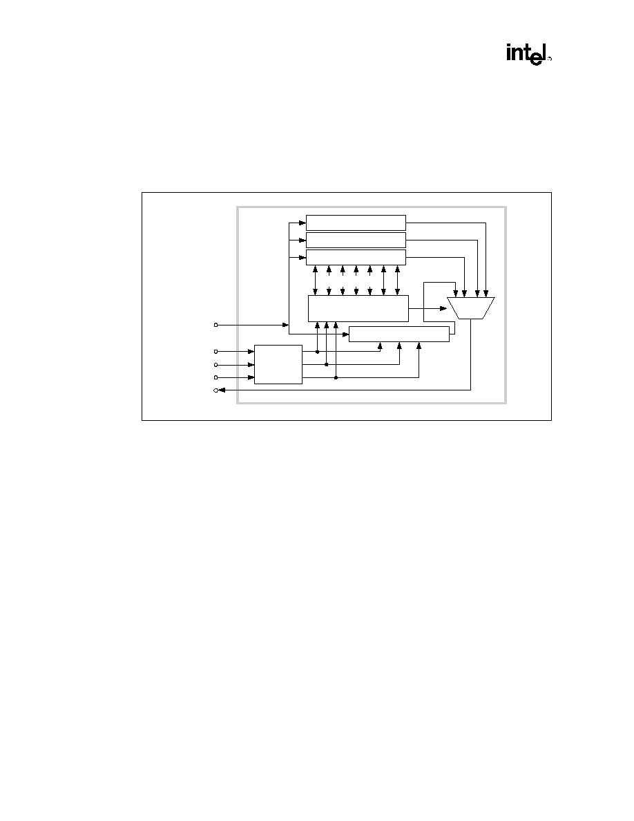
Testability
10-2
Intel
Æ
E8870SP Scalability Port Switch (SPS) Datasheet
A simplified block diagram of the TAP used in the the E8870 chipset components is shown in
Figure 10-2
. This TAP logic consists of a finite state machine controller, a serially-accessible
instruction register, instruction decode logic, and data registers. The set of data registers includes
those described in the 1149.1 standard (the bypass register, device ID register, etc.), plus chipset-
specific additions. The private data registers used to control the test and debug features are not
shown.
10.1.2
Accessing the TAP Logic
The TAP is accessed through an IEEE 1149.1-compliant TAP controller finite state machine. This
finite state machine, shown in
Figure 10-3
, contains a reset state, a run-test/idle state, and two
major branches. These branches allow access either to the TAP Instruction register or to one of the
data registers. The TMS pin is used as the controlling input to traverse this finite state machine.
TAP instructions and test data are loaded serially (in the Shift-IR and Shift-DR states, respectively)
using the TDI pin. State transitions are made on the rising edge of TCK.
The following is a brief description of each of the states of the TAP controller state machine. Refer
to the IEEE 1149.1 standard for detailed descriptions of the states and their operation.
∑
Test-Logic-Reset: In this state, the test logic is disabled so that the processor operates
normally. In this state, the instruction in the Instruction register is forced to IDCODE.
Regardless of the original state of the TAP Finite State Machine (TAPFSM), it always enters
Test-Logic-Reset when the TMS input is held asserted for at least five clocks. The controller
also enters this state immediately when the TRST# pin is asserted, and automatically upon
power-on. The TAPFSM cannot leave this state as long as the TRST# pin is held asserted.
∑
Run-Test/Idle: A controller state between scan operations. Once entered the controller will
remain in this state as long as TMS is held low. In this state, activity in selected test logic
occurs only in the presence of certain instructions. For instructions that do not cause functions
to execute in this state, all test data registers selected by the current instructions retain their
previous state.
∑
Select-IR-Scan: This is a temporary controller state in which all test data registers selected by
the current instruction retain their previous state.
Figure 10-2. Simplified Block Diagram of TAP Controller
001332
Boundary Scan Register
Device Identification
BYPASS Register
Instruction Decode/
Control Logic
Instruction Register
TAP
Controller
Machine
TDO
Mux
TDI
TMS
TCK
TRST#
TDO
Control Signals
Intel
Æ
E8870SP Scalability Port Switch (SPS) Datasheet
10-3
Testability
∑
Capture-IR: In this state, the shift register contained in the Instruction register loads a fixed
value (of which the two least significant bits are "01") on the rising edge of TCK. The parallel,
latched output of the Instruction register (current instruction) does not change in this state.
∑
Shift-IR: The shift register contained in the Instruction register is connected between TDI and
TDO and is shifted one stage toward its serial output on each rising edge of TCK. The output
arrives at TDO on the falling edge of TCK. The current instruction does not change in this
state.
∑
Exit-IR: This is a temporary state and the current instruction does not change in this state.
∑
Pause-IR: Allows shifting of the Instruction register to be temporarily halted. The current
instruction does not change in this state.
∑
Exit2-IR: This is a temporary state and the current instruction does not change in this state.
∑
Update-IR: The instruction which has been shifted into the Instruction register is latched into
the parallel output of the Instruction register on the falling edge of TCK. Once the new
instruction has been latched, it remains the current instruction until the next Update-IR (or
until the TAPFSM is reset).
Figure 10-3. TAP Controller State Diagram
000683
Select-
DR-Scan
Capture-DR
Shift-DR
Exit1-DR
Pause-DR
Exit2-DR
0
0
1
0
1
1
1
0
0
0
Update-DR
1
Select-
IR-Scan
Capture-IR
Shift-IR
Exit1-IR
Pause-IR
Exit2-IR
0
0
1
0
1
1
1
0
0
0
Update-IR
1
Run-Test/
Idle
Test-Logic-
Reset
0
1
1
0
0
1 TMS
1
0
1
Testability
10-4
Intel
Æ
E8870SP Scalability Port Switch (SPS) Datasheet
∑
Select-DR-Scan: This is a temporary controller state and all test data registers selected by the
current instruction retain their previous values.
∑
Capture-DR: In this state, data may be parallel-loaded into test data registers selected by the
current instruction on the rising edge of TCK. If a test data register selected by the current
instruction does not have a parallel input, or if capturing is not required for the selected test,
then the register retains its previous state.
∑
Shift-DR: The data register connected between TDI and TDO as a result of selection by the
current instruction is shifted one stage toward its serial output on each rising edge of TCK. The
output arrives at TDO on the falling edge of TCK. If the data register has a latched parallel
output then the latch value does not change while new data is being shifted in.
∑
Exit1-DR: This is a temporary state and all data registers selected by the current instruction
retain their previous values.
∑
Pause-DR: Allows shifting of the selected data register to be temporarily halted without
stopping TCK. All registers selected by the current instruction retain their previous values.
∑
Exit2-DR: This is a temporary state and all registers selected by the current instruction retain
their previous values.
∑
Update-DR: Some test data registers may be provided with latched parallel outputs to prevent
changes in the parallel output while data is being shifted in the associated shift register path in
response to certain instructions. Data is latched into the parallel output of these registers from
the shift-register path on the falling edge of TCK.
10.2
Public TAP Instructions
Table 10-2
contains descriptions of the encoding and operation of the public TAP instructions.
There are four 1149.1-defined instructions implemented in the E8870 chipset device. These
instructions select from among three different TAP data registers ≠ the boundary scan, device ID,
and bypass registers. The public instructions can be executed with only the standard connection of
the JTAG port pins. This means the only clock required will be TCK. Full details of the operation
of these instructions can be found in the 1149.1 standard. The opcodes are 1149.1-compliant, and
are consistent with the Intel-standard encodings.
Refer to
Table 10-2
for a brief description of each instruction. For more thorough descriptions refer
to the IEEE 1149.1 specification.
Table 10-2. Public TAP Instructions
Instruction
Encoding
Data Register
Selected
Description
BYPASS
1111111
Bypass
The BYPASS command selects the bypass register, a single bit
register connected between TDI and TDO pins. This allows more
rapid movement of test data to and from other components in the
system.
EXTEST
0000000
Boundary
Scan
The EXTEST Instruction allows circuitry or wiring external to the
devices to be tested. Boundary scan register cells at outputs are
used to apply stimulus while boundary scan cells at input pins
are used to capture data.

Intel
Æ
E8870SP Scalability Port Switch (SPS) Datasheet
10-5
Testability
10.3
TAP Registers
The following is a description of all test registers which can be accessed through the TAP.
∑
Boundary Scan Register: The boundary scan register consists of several single-bit shift
registers. The boundary scan register provides a shift register path from all the input to the
output pins on the SPS. Data is transferred from TDI to TDO through the boundary scan
register.
∑
Bypass Register: The bypass register is a one-bit shift register that provides the minimal path
length between TDI and TDO. The bypass register is selected when no test operation is being
performed by a component on the board. The bypass register loads a logic zero at the start of a
scan cycle.
∑
Device Identification (ID) Register: The device ID register contains the manufacturer's
identification code, version number, and part number. The device ID register has a fixed length
of 32 bits, as defined by the IEEE 1149.1 specification.
∑
Instruction Register: This register consists of a 7-bit shift register (connected between TDI
and TDO), and the actual instruction register (which is loaded in parallel from the shift
register). The parallel output of the TAP instruction register goes to the TAP instruction
decoder shown in
Figure 10-4
.
∑
Configuration Access Register: This register allows SNC to access the configuration
registers via the JTAG TAP. An acceptable configuration access chain format is shown.
SAMPLE/
PRELOAD
0000001
Boundary
Scan
The SAMPLE/PRELOAD Instruction is used to allow scanning of
the boundary scan register without causing interference to the
normal operation of the device. Two functions can be performed
by use of the Sample/Preload Instruction.
SAMPLE ≠ allows a snapshot of the data flowing into & out of the
device to be taken without affecting the normal operation of the
device.
PRELOAD ≠ allows an initial pattern to be placed into the
boundary scan register cells. This allows initial known data to be
present prior to the selection of another boundary-scan test
operation.
IDCODE
0000010
IDCODE
The IDCODE instruction is forced into the parallel output latches
of the instruction register during the Test-Logic-Reset Tap state.
This allows the device identification register to be selected by
manipulation of the broadcast TMS and TCK signals for testing
purposes, as well as by a conventional instruction register scan
operation.
CLAMP
0000100
Boundary
Scan
This allows static "guarding values" to be set onto components
that are not specifically being tested while maintaining the
bypass register as the serial path through the device.
HIGHZ
0001000
Boundary
Scan
The HIGHZ Instruction is used to force all outputs of the device
(except TDO) into a high impedance state. This instruction shall
select the bypass register to be connected between TDI and
TDO in the Shift-DR controller state.
Table 10-2. Public TAP Instructions (Continued)
Instruction
Encoding
Data Register
Selected
Description
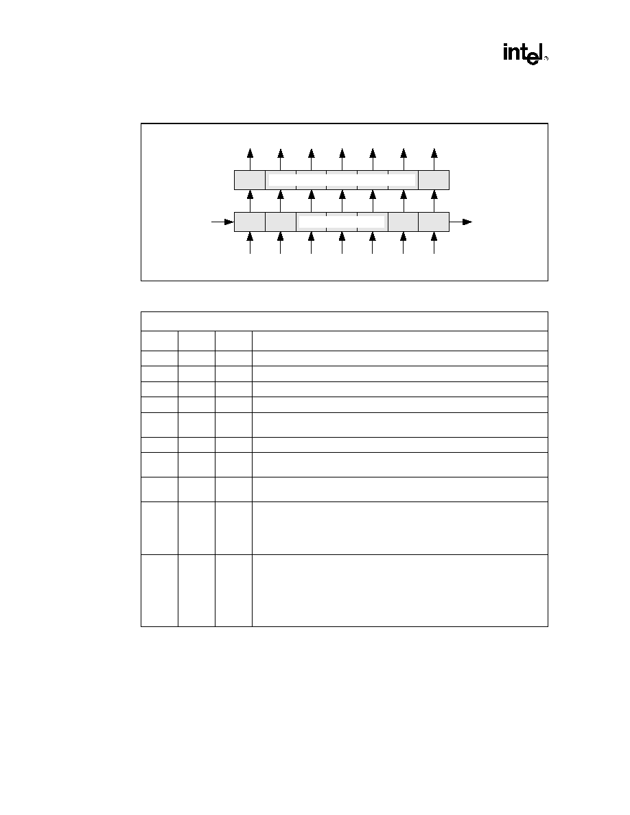
Testability
10-6
Intel
Æ
E8870SP Scalability Port Switch (SPS) Datasheet
Figure 10-4. TAP Instruction Register
001331
Table 10-3. Example of Configuration Access Data Register Format
JCONF Encode: 1000010
Bit
Attr
Default
Description
63:56
RW
00h
Data Byte3: MSB of the read/write data, Data[31:24]
55:48
RW
00h
Data Byte2: Next MSB of the read/write data, Data[23:16]
47:40
RW
00h
Data Byte1: Next LSB of the read/write data, Data[15:8]
39:32
RW
00h
Data Byte0: LSB of the read/write data, Data[7:0]
31:24
RW
00h
Register Address: Address of a register located in a device on a bus within a
group of registers assign to a function.
23:19
RW
00h
Device ID: PCI equivalent to uniquely identify a device on a bus.
18:16
RW
000
Function Number: PCI equivalent of a function number to obtain access to
register banks within a device.
15:8
RW
00h
Bus Number: PCI equivalent of a bus number to recognize devices connected
to this bus.
7:4
RW
0h
Status:
[7]: Error bit set when a config request returns a Hard Fail condition.
[6:5]: Reserved
[4]: Busy bit. Set when read or write operation is in progress.
3:0
RW
0h
Command:
0xxx = NOP used in polling the chain to determine if the unit is busy.
1001 = write byte
1010 = write word
1011 = write dword
1100 = read dword
LSB
MSB
Shift Register
Fixed Capture Value
TDO
TDI
Parallel Output
Actual Instruction Register