
Intel
Æ
Wireless Flash Memory (W18)
28F320W18, 28F640W18, 28F128W18
Datasheet
Product Features
The Intel
Æ
Wireless Flash Memory (W18) device with flexible multi-partition dual operation,
provides high-performance asynchronous and synchronous burst reads. It is an ideal memory for
low-voltage burst CPUs. Combining high read performance with flash memory's intrinsic non-
volatility, the W18 device eliminates the traditional system-performance paradigm of shadowing
redundant code memory from slow nonvolatile storage to faster execution memory. It reduces
the total memory requirement that increases reliability and reduces overall system power
consumption and cost.
The W18 device's flexible multi-partition architecture allows programming or erasing to occur
in one partition while reading from another partition. This allows for higher data write
throughput compared to single partition architectures. The dual-operation architecture also
allows two processors to interleave code operations while program and erase operations take
place in the background. The designer can also choose the size of the code and data partitions via
the flexible multi-partition architecture.
High Performance Read-While-Write/
Erase
-- Burst frequency at 66 MHz
-- 60 ns Initial Access Read Speed
-- 11 ns Burst-Mode Read Speed
-- 20 ns Page-Mode Read Speed
-- 4-, 8-, 16-, and Continuous-Word Burst
Mode Reads
-- Burst and Page Mode Reads in all
Blocks, across all partition boundaries
-- Burst Suspend Feature
-- Enhanced Factory Programming at
3.1 µs/word (typ.for 0.13 µm)
Security
-- 128-bit Protection Register
-- 64-bits Unique Programmed by Intel
-- 64-bits User-Programmable
-- Absolute Write Protection with V
PP
at
Ground
-- Individual and Instantaneous Block
Locking/Unlocking with Lock-Down
Capability
Quality and Reliability
-- Temperature Range: ≠40 ∞C to +85 ∞C
-- 100k Erase Cycles per Block
-- 0.13 µ m ETOXTM VIII Process
-- 0.18 µ m ETOXTM VII Process
Architecture
-- Multiple 4-Mbit Partitions
-- Dual Operation: RWW or RWE
-- 8KB parameter blocks
-- 64KB main blocks
-- Top or Bottom Parameter Devices
-- 16-bit wide data bus
Software
-- 5 µs (typ.) Program and Erase Suspend
Latency Time
-- Flash Data Integrator (FDI) and Common
Flash Interface (CFI) Compatible
-- Programmable WAIT Signal Polarity
Packaging and Power
-- 0.13 µm: 32-, 64-, and 128-Mbit in VF
BGA Package; 128-Mbit in QUAD+
Package
-- 0.18 µm: 32- and 128-Mbit Densities in
VF BGA Package; 64-Mbit Density in
µBGA* Package
-- 56 Active Ball Matrix, 0.75 mm Ball-
Pitch
-- V
CC
= 1.70 V to 1.95 V
-- V
CCQ
= 1.70 V to 2.24 V or 1.35 V to
1.80 V
-- Standby current (0.13 µm): 8µA (typ.)
-- Read current: 7mA (typ.)
290701-009
December 2003
Notice: This document contains information on new products in production. The specifications
are subject to change without notice. Verify with your local Intel sales office that you have the
latest datasheet before finalizing a design.

2
Datasheet
INFORMATION IN THIS DOCUMENT IS PROVIDED IN CONNECTION WITH INTELÆ PRODUCTS. NO LICENSE, EXPRESS OR IMPLIED, BY
ESTOPPEL OR OTHERWISE, TO ANY INTELLECTUAL PROPERTY RIGHTS IS GRANTED BY THIS DOCUMENT. EXCEPT AS PROVIDED IN
INTEL'S TERMS AND CONDITIONS OF SALE FOR SUCH PRODUCTS, INTEL ASSUMES NO LIABILITY WHATSOEVER, AND INTEL DISCLAIMS
ANY EXPRESS OR IMPLIED WARRANTY, RELATING TO SALE AND/OR USE OF INTEL PRODUCTS INCLUDING LIABILITY OR WARRANTIES
RELATING TO FITNESS FOR A PARTICULAR PURPOSE, MERCHANTABILITY, OR INFRINGEMENT OF ANY PATENT, COPYRIGHT OR OTHER
INTELLECTUAL PROPERTY RIGHT. Intel products are not intended for use in medical, life saving, or life sustaining applications.
Intel may make changes to specifications and product descriptions at any time, without notice.
The 1.8 Volt IntelÆ wireless flash memory datasheet may contain design defects or errors known as errata which may cause the product to deviate
from published specifications. Current characterized errata are available on request.
Contact your local Intel sales office or your distributor to obtain the latest specifications and before placing your product order.
Copies of documents which have an ordering number and are referenced in this document, or other Intel literature may be obtained by calling 1-800-
548-4725 or by visiting Intel's website at http://www.intel.com.
Copyright © 2003, Intel Corporation.
*Other names and brands may be claimed as the property of others.

Datasheet
3
Contents
Contents
1.0
Introduction
...............................................................................................................................9
1.1
Document Purpose ............................................................................................................... 9
1.2
Nomenclature ....................................................................................................................... 9
1.3
Conventions .......................................................................................................................... 9
2.0
Device Description
................................................................................................................10
2.1
Product Overview ...............................................................................................................10
2.2
Package Diagram ...............................................................................................................12
2.3
Signal Descriptions ............................................................................................................. 14
2.4
Memory Map and Partitioning ............................................................................................. 15
3.0
Device Operations
................................................................................................................. 18
3.1
Bus Operations ................................................................................................................... 18
3.1.1
Read ...................................................................................................................... 18
3.1.2
Burst Suspend ....................................................................................................... 19
3.1.3
Standby.................................................................................................................. 19
3.1.4
Reset ..................................................................................................................... 19
3.1.5
Write ...................................................................................................................... 20
3.2
Device Commands ............................................................................................................. 20
3.3
Command Sequencing ....................................................................................................... 24
4.0
Read Operations
.................................................................................................................... 25
4.1
Read Array..........................................................................................................................25
4.2
Read Device ID................................................................................................................... 25
4.3
Read Query (CFI) ...............................................................................................................26
4.4
Read Status Register..........................................................................................................26
4.5
Clear Status Register.......................................................................................................... 28
5.0
Program Operations
............................................................................................................. 28
5.1
Word Program .................................................................................................................... 28
5.2
Factory Programming ......................................................................................................... 29
5.3
Enhanced Factory Program (EFP) ..................................................................................... 30
5.3.1
EFP Requirements and Considerations................................................................. 30
5.3.2
Setup ..................................................................................................................... 31
5.3.3
Program ................................................................................................................. 31
5.3.4
Verify...................................................................................................................... 31
5.3.5
Exit ......................................................................................................................... 32
6.0
Program and Erase Operations
....................................................................................... 34
6.1
Program/Erase Suspend and Resume ...............................................................................34
6.2
Block Erase......................................................................................................................... 36
6.3
Read-While-Write and Read-While-Erase .......................................................................... 38
7.0
Security Modes
....................................................................................................................... 39
7.1
Block Lock Operations ........................................................................................................ 39
7.1.1
Lock ....................................................................................................................... 40
7.1.2
Unlock .................................................................................................................... 40

Contents
4
Datasheet
7.1.3
Lock-Down............................................................................................................. 40
7.1.4
Block Lock Status .................................................................................................. 41
7.1.5
Lock During Erase Suspend .................................................................................. 41
7.1.6
Status Register Error Checking ............................................................................. 41
7.1.7
WP# Lock-Down Control ....................................................................................... 42
7.2
Protection Register ............................................................................................................. 42
7.2.1
Reading the Protection Register............................................................................ 43
7.2.2
Programing the Protection Register....................................................................... 43
7.2.3
Locking the Protection Register............................................................................. 44
7.3
VPP Protection ................................................................................................................... 45
8.0
Set Configuration Register
................................................................................................ 46
8.1
Read Mode (CR[15])........................................................................................................... 48
8.2
First Access Latency Count (CR[13:11]) ............................................................................ 48
8.2.1
Latency Count Settings.......................................................................................... 49
8.3
WAIT Signal Polarity (CR[10]) ............................................................................................ 50
8.4
WAIT Signal Function ......................................................................................................... 50
8.5
Data Hold (CR[9]) ............................................................................................................... 51
8.6
WAIT Delay (CR[8]) ............................................................................................................ 52
8.7
Burst Sequence (CR[7])...................................................................................................... 52
8.8
Clock Edge (CR[6])............................................................................................................. 54
8.9
Burst Wrap (CR[3]) ............................................................................................................. 54
8.10
Burst Length (CR[2:0])........................................................................................................ 54
9.0
Power Consumption
............................................................................................................. 55
9.1
Active Power....................................................................................................................... 55
9.2
Automatic Power Savings (APS) ........................................................................................ 55
9.3
Standby Power ................................................................................................................... 55
9.4
Power-Up/Down Characteristics......................................................................................... 55
9.4.1
System Reset and RST# ....................................................................................... 56
9.4.2
VCC, VPP, and RST# Transitions ......................................................................... 56
9.5
Power Supply Decoupling................................................................................................... 56
10.0 Thermal and DC Characteristics
..................................................................................... 57
10.1
Absolute Maximum Ratings ................................................................................................ 57
10.2
Operating Conditions .......................................................................................................... 57
10.3
DC Current Characteristics (.13
µ
and .18 µ
µ
)................................................................. 58
10.4
DC Voltage Characteristics................................................................................................. 60
11.0 AC Characteristics
................................................................................................................ 62
11.1
Read Operations ≠ .13
µµ
............................................................................ 62
11.2
Read Operations ≠ .18
µµ
............................................................................ 64
11.3
AC Write Characteristics..................................................................................................... 74
11.4
Erase and Program Times.................................................................................................. 79
11.5
Reset Specifications ........................................................................................................... 80
11.6
AC I/O Test Conditions ....................................................................................................... 81
11.7
Device Capacitance............................................................................................................ 82
Appendix A Write State Machine States
............................................................................... 83
Appendix B Common Flash Interface
.................................................................................... 86

Datasheet
5
Contents
Appendix C Mechanical Specifications
................................................................................. 95
Appendix D Ordering Information
.........................................................................................100

Contents
6
Datasheet
Revision History
Date of
Revision
Version
Description
09/13/00
-001
Initial Release
01/29/01
-002
Deleted 16-Mbit density
Revised ADV#, Section 2.2
Revised Protection Registers, Section 4.16
Revised Program Protection Register, Section 4.18
Revised Example in First Access Latency Count, Section 5.0.2
Revised Figure 5, Data Output with LC Setting at Code 3
Added WAIT Signal Function, Section 5.0.3
Revised WAIT Signal Polarity, Section 5.0.4
Revised Data Output Configuration, Section 5.0.5
Added Figure 7, Data Output Configuration with WAIT Signal Delay
Revised WAIT Delay Configuration, Section 5.0.6
Changed V
CCQ
Spec from 1.7 V ≠ 1.95 V to 1.7 V ≠ 2.24 V in Section 8.2,
Extended Temperature Operation
Changed I
CCS
Spec from 15 µA to 18 µA in Section 8.4, DC
Characteristics
Changed I
CCR
Spec from 10 mA (CLK = 40 MHz, burst length = 4) and 13
mA (CLK = 52 MHz, burst length = 4) to 13 mA, and 16 mA respectively in
Section 8.4, DC Characteristics
Changed I
CCWS
Spec from 15 µA to 18 µA in Section 8.4, DC
Characteristics
Changed I
CCES
Spec from 15 µA to 18 µA in Section 8.4, DC
Characteristics
Changed t
CHQX
Spec from 5ns to 3ns in Section 8.6, AC Read
Characteristics
Added Figure 25, WAIT Signal in Synchronous Non-Read Array Operation
Waveform
Added Figure 26, WAIT Signal in Asynchronous Page Mode Read
Operation Waveform
Added Figure 27, WAIT Signal in Asynchronous Single Word Read
Operation Waveform
Revised Appendix E, Ordering Information
06/12/01
-003
Revised entire Section 4.10, Enhanced Factory Program Command (EFP)
and Figure 6, Enhanced Factory Program Flowchart
Revised Section 4.13, Protection Register
Revised Section 4.15, Program Protection Register
Revised Section 7.3, Capacitance, to include 128-Mbit specs
Revised Section 7.4, DC Characteristics, to include 128-Mbit specs
Revised Section 7.6, AC Read Characteristics, to include 128-Mbit device
specifications
Added t
VHGL
Spec in Section 7.6, AC Read Characteristics
Revised Section 7.7, AC Write Characteristics, to include 128-Mbit device
specifications
Minor text edits

Datasheet
7
Contents
04/05/02
-004
New Sections Organization
Added 16 Word Burst Feature
Added Burst Suspend Section
Revised Block Locking State Diagram
Revised Active Power Section
Revised Automatic Power Savings Section
Revised Power-Up/Down Operation Section
Revised Extended Temperature Operation
Added 128Mb DC Characteristics Table
Added 128 Mb AC Read Characteristics
Revised Table 17. Test Configuration Component Values for Worst Case
Speed Conditions
Added .13 µ Product DC and AC Read Characteristics
Revised AC Write Characteristics
Added Read to Write and Write to Read Transition Waveforms
Revised Reset Specifications
Various text edits
10/10/02
-005
Various text edits
Updated Latency Count Section, including adding Latency Count Tables
Added section 8.4 WAIT Function and WAIT Summary Table
Updated Package Drawing and Dimensions
11/12/02
-006
Various text clarifications
01/14/03
-007
Removed Intel Burst Order
Revised Table 22, DC Current Characteristics, I
CCS
Revised Table 22, DC Current Characteristics, I
CCAPS
Various text edits
03/21/03
-008
Revised Table 22, Read Operations, t
APA
Added note to table 15, Configuration Register Descriptions
Added note to section 3.1.1, Read
12/17/03
-009
Updated Block-Lock Operations (Section 7.1 and Figure 11)
Updated Table 21 (128Mb I
CCR
)
Updated Table 4 (WAIT behavior)
Added QUAD+ ballout, package mechanicals, and order information
Various text edits including latest product-naming convention
Date of
Revision
Version
Description

Contents
8
Datasheet

Intel
Æ
Wireless Flash Memory (W18)
Datasheet
9
1.0
Introduction
1.1
Document Purpose
This datasheet contains information about the 1.8 Volt Intel
Æ
Wireless Flash memory (W18) device
family. Section 1.0 provides a flash memory overview.
Section 2.0
through
Section 9.0
describe the
memory functionality.
Section 10.0
describes the electrical specifications for extended temperature
product offerings. Packaging specifications and order information can be found in
Appendix C
and
Appendix D
, respectively.
1.2
Nomenclature
Many acronyms that describe product features or usage are defined here:
∑
APS - Automatic Power Savings
∑
BBA - Block Base Address
∑
CFI - Common Flash Interface
∑
CUI - Command User Interface
∑
EFP - Enhanced Factory Programming
∑
FDI - Flash Data Integrator
∑
NC - No Connect
∑
OTP - One-Time Programmable
∑
PBA - Partition Base Address
∑
RWE - Read-While-Erase
∑
RWW - Read-While-Write
∑
SRD - Status Register Data
∑
VF BGA - Very thin, Fine pitch, Ball Grid Array
∑
WSM - Write State Machine
1.3
Conventions
Many abbreviated terms and phrases are used throughout this document:
∑
The term "1.8 V" refers to the full VCC voltage range of 1.7 V ≠ 1.95 V (except where noted)
and "V
PP
= 12 V" refers to 12 V ±5%.
∑
When referring to registers, the term set means the bit is a logical 1, and clear means the bit is
a logical 0.
∑
The terms pin and signal are often used interchangeably to refer to the external signal
connections on the package. (ball is the term used for VF BGA).
∑
A word is 2 bytes, or 16 bits.

Intel
Æ
Wireless Flash Memory (W18)
10
Datasheet
∑
Signal names are in all CAPS (see
Section 2.3, "Signal Descriptions" on page 14
.)
∑
Voltage applied to the signal is subscripted, for example, V
PP
.
Throughout this document, references are made to top, bottom, parameter, and partition. To clarify
these references, the following conventions have been adopted:
∑
A block is a group of bits (or words) that erase simultaneously with one block erase
instruction.
∑
A main block contains 32 Kwords.
∑
A parameter block contains 4 Kwords.
∑
The Block Base Address (BBA) is the first address of a block.
∑
A partition is a group of blocks that share erase and program circuitry and a common status
register.
∑
The Partition Base Address (PBA) is the first address of a partition. For example, on a 32-
Mbit top-parameter device, partition number 5 has a PBA of 140000h.
∑
The top partition is located at the highest physical device address. This partition may be a
main partition or a parameter partition.
∑
The bottom partition is located at the lowest physical device address. This partition may be a
main partition or a parameter partition.
∑
A main partition contains only main blocks.
∑
A parameter partition contains a mixture of main blocks and parameter blocks.
∑
A top parameter device (TPD) has the parameter partition at the top of the memory map with
the parameter blocks at the top of that partition. This was formerly referred to as top-boot
device.
∑
A bottom parameter device (BPD) has the parameter partition at the bottom of the memory
map with the parameter blocks at the bottom of that partition. This was formerly referred to as
bottom-boot block flash device.
2.0
Device Description
This section provides an overview of the W18 device features, packaging, signal naming, and
device architecture.
2.1
Product Overview
The W18 device provides Read-While-Write (RWW) and Read-White-Erase (RWE) capability
with high-performance synchronous and asynchronous reads on package-compatible densities with
a 16-bit data bus. Individually-erasable memory blocks are optimally sized for code and data
storage. Eight 4-Kword parameter blocks are located in the parameter partition at either the top or
bottom of the memory map. The rest of the memory array is grouped into 32-Kword main blocks.
The memory architecture for the W18 device consists of multiple 4-Mbit partitions, the exact
number depending on device density. By dividing the memory array into partitions, program or
erase operations can take place simultaneously during read operations. Burst reads can traverse

Intel
Æ
Wireless Flash Memory (W18)
Datasheet
11
partition boundaries, but user application code is responsible for ensuring that they don't extend
into a partition that is actively programming or erasing. Although each partition has burst-read,
write, and erase capabilities, simultaneous operation is limited to write or erase in one partition
while other partitions are in a read mode.
Augmented erase-suspend functionality further enhances the RWW capabilities of this device. An
erase can be suspended to perform a program or read operation within any block, except that which
is erase-suspended. A program operation nested within a suspended erase can subsequently be
suspended to read yet another memory location.
After device power-up or reset, the W18 device defaults to asynchronous read configuration.
Writing to the device's configuration register enables synchronous burst-mode read operation. In
synchronous mode, the CLK input increments an internal burst address generator. CLK also
synchronizes the flash memory with the host CPU and outputs data on every, or on every other,
valid CLK cycle after an initial latency. A programmable WAIT output signals to the CPU when
data from the flash memory device is ready.
In addition to its improved architecture and interface, the W18 device incorporates Enhanced
Factory Programming (EFP), a feature that enables fast programming and low-power designs. The
EFP feature provides the fastest currently-available program performance, which can increase a
factory's manufacturing throughput.
The device supports read operations at 1.8 V and erase and program operations at 1.8 V or 12 V.
With the 1.8-V option, VCC and VPP can be tied together for a simple, ultra-low-power design. In
addition to voltage flexibility, the dedicated VPP input provides complete data protection when
V
PP
V
PPLK
.
This device allows I/O operation at voltages even lower than the minimum V
CCQ
of 1.7 V. This
Extended V
CCQ
range, 1.35 V ≠ 1.8 V, permits even greater system design flexibility.
A 128-bit protection register enhances the user's ability to implement new security techniques and
data protection schemes. Unique flash device identification and fraud-, cloning-, or content-
protection schemes are possible through a combination of factory-programmed and user-OTP data
cells. Zero-latency locking/unlocking on any memory block provides instant and complete
protection for critical system code and data. An additional block lock-down capability provides
hardware protection where software commands alone cannot change the block's protection status.
The device's Command User Interface (CUI) is the system processor's link to internal flash
memory operation. A valid command sequence written to the CUI initiates device Write State
Machine (WSM) operation that automatically executes the algorithms, timings, and verifications
necessary to manage flash memory program and erase. An internal status register provides ready/
busy indication results of the operation (success, fail, and so on).
Three power-saving features≠ Automatic Power Savings (APS), standby, and RST#≠ can
significantly reduce power consumption. The device automatically enters APS mode following
read cycle completion. Standby mode begins when the system deselects the flash memory by
de-asserting CE#. Driving RST# low produces power savings similar to standby mode. It also
resets the part to read-array mode (important for system-level reset), clears internal status registers,
and provides an additional level of flash write protection.
Intel
Æ
Wireless Flash Memory (W18)
12
Datasheet
2.2
Package Diagram
The W18 device is available in a 56-ball VF BGA and µBGA Chip SCale Package with 0.75 mm
ball pitch, or the 88-ball (80 active balls) QUAD+ SCSP package.
Figure 1
shows the device
ballout for the VF BGA and µBGA package.
Figure 2
shows the device ballout for the QUAD+
package.
Figure 1. 56-Ball VF BGA / µBGA Ballout
NOTES:
1. On lower density devices, upper address balls can be treated as NC. (Example: For 32-Mbit density, A21 and A22 will be NC).
2. See
Appendix C, "Mechanical Specifications" on page 95
for mechanical specifications for the package.
A
B
C
D
E
F
G
A
B
C
D
E
F
G
Top View - Ball Side Down
Complete Ink Mark Not Shown
8
7
6
5
4
3
2
1
1
2
3
4
5
6
7
8
Bottom View - Ball Side Up
A4
A6
A18
VPP
VCC
VSS
A8
A11
A3
A5
A17
RST#
CLK
A20
A9
A12
A2
A7
WE#
ADV#
A19
A10
A13
A1
A14
WP#
DQ12
A16
WAIT
A15
A0
CE#
DQ1
DQ2
DQ4
DQ6
DQ15
VCCQ
OE#
DQ0
DQ9
DQ10
DQ11
DQ13 DQ14
VSS
VSSQ
DQ8
VCCQ
DQ3
VCC
DQ5
VSSQ
DQ7
A22
A21
A4
A6
A18
VPP
VCC
VSS
A8
A11
A3
A5
A17
RST#
CLK
A20
A9
A12
A2
A7
WE#
ADV#
A19
A10
A13
A1
A14
WP#
DQ12
A16
WAIT
A15
A0
CE#
DQ1
DQ2
DQ4
DQ6
DQ15
VCCQ
OE#
DQ0
DQ9
DQ10
DQ11
DQ13
DQ14
VSS
VSSQ
DQ8
VCCQ
DQ3
VCC
DQ5
VSSQ
DQ7
A22
A21
Intel
Æ
Wireless Flash Memory (W18)
Datasheet
13
Figure 2. 88-Ball (80 Active Balls) QUAD+ Ballout
NOTES:
1. Unused upper address balls can be treated as NC (for 128Mbit, A[25:23] are not used).
2. See
Appendix C, "Mechanical Specifications" on page 95
for mechanical specifications for the package.
Flash specific
SRAM/PSRAM specific
Global
Legend:
Top View - Ball Side Down
8
7
6
5
4
3
2
1
A
B
C
D
E
F
G
H
J
K
L
M
DU
A4
DU
DU
DU
DU
DU
DU
DU
A5
A3
A2
A7
A1
A6
A0
A18
A19
VSS
VSS
A23
A24
A25
A17
F2-VCC
CLK
A21
A22
A12
A11
A13
A9
P1-CS#
F-VPP,
F-VPEN
A20
A10
A15
F-WE#
A8
D8
D2
D10
D5
D13
WAIT
A14
A16
F1-CE#
P-Mode,
P-CRE
VSS
VSS
VSS
P2-CS#
F1-VCC
F2-VCC
VCCQ
F3-CE#
D0
D1
D9
D3
D4
D6
D7
D15
D11
D12
D14
F1-OE#
F2-OE#
P-VCC
S-CS2
R-WE#
R-UB#
R-LB#
R-OE#
S-VCC
S-CS1#
F1-VCC
F-WP#
ADV#
F-RST#
F2-CE#
VCCQ
VSS
VSS
VCCQ
VSS

Intel
Æ
Wireless Flash Memory (W18)
14
Datasheet
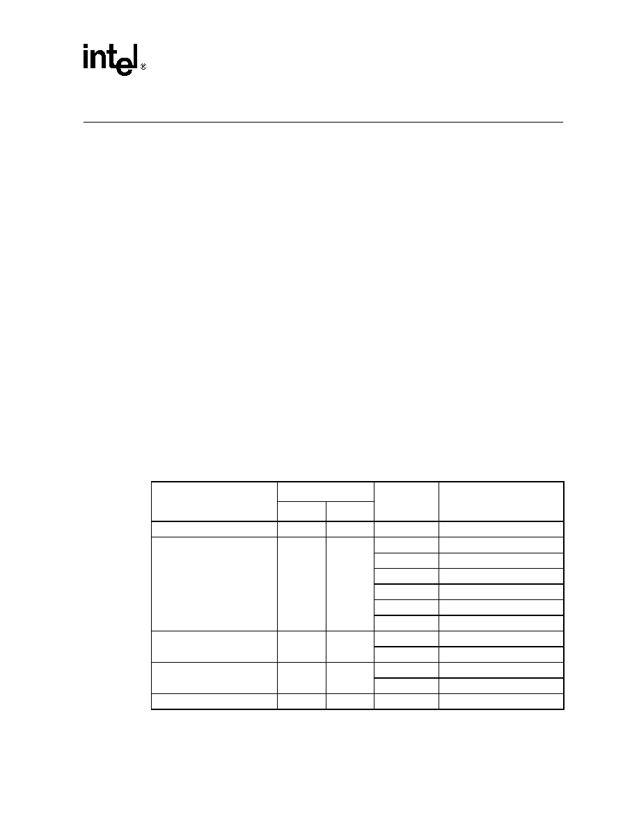
2.3
Signal Descriptions
Table 1
describes ball usage.
Table 1.
Signal Descriptions
Symbol
Type
Name and Function
A[22:0]
I
ADDRESS INPUTS: For memory addresses. 32 Mbit: A[20:0]; 64 Mbit: A[21:0]; 128 Mbit: A[22:0]
D[15:0]
I/O
DATA INPUTS/OUTPUTS: Inputs data and commands during write cycles; outputs data during
memory, status register, protection register, and configuration code reads. Data pins float when the
chip or outputs are deselected. Data is internally latched during writes.
ADV#
I
ADDRESS VALID: ADV# indicates valid address presence on address inputs. During synchronous
read operations, all addresses are latched on ADV#'s rising edge or the next valid CLK edge with
ADV# low, whichever occurs first.
CE#
I
CHIP ENABLE: Asserting CE# activates internal control logic, I/O buffers, decoders, and sense amps.
De-asserting CE# deselects the device, places it in standby mode, and tri-states all outputs.
CLK
I
CLOCK: CLK synchronizes the device to the system bus frequency during synchronous reads and
increments an internal address generator. During synchronous read operations, addresses are latched
on ADV#'s rising edge or the next valid CLK edge with ADV# low, whichever occurs first.
OE#
I
OUTPUT ENABLE: When asserted, OE# enables the device's output data buffers during a read cycle.
When OE# is deasserted, data outputs are placed in a high-impedance state.
RST#
I
RESET: When low, RST# resets internal automation and inhibits write operations. This provides data
protection during power transitions. de-asserting RST# enables normal operation and places the
device in asynchronous read-array mode.
WAIT
O
WAIT: The WAIT signal indicates valid data during synchronous read modes. It can be configured to be
asserted-high or asserted-low based on bit 10 of the Configuration Register. WAIT is tri-stated if CE# is
deasserted. WAIT is not gated by OE#.
WE#
I
WRITE ENABLE: WE# controls writes to the CUI and array. Addresses and data are latched on the
rising edge of WE#.
WP#
I
WRITE PROTECT: Disables/enables the lock-down function. When WP# is asserted, the lock-down
mechanism is enabled and blocks marked lock-down cannot be unlocked through software. See
Section 7.1, "Block Lock Operations" on page 39
for details on block locking.
VPP
Pwr/I
ERASE AND PROGRAM POWER: A valid voltage on this pin allows erasing or programming. Memory
contents cannot be altered when V
PP
V
PPLK
. Block erase and program at invalid V
PP
voltages should
not be attempted.
Set V
PP
= V
CC
for in-system program and erase operations. To accommodate resistor or diode drops
from the system supply, the V
IH
level of V
PP
can be as low as V
PP1
min. V
PP
must remain above V
PP1
min to perform in-system flash modification. VPP may be 0 V during read operations.
V
PP2
can be applied to main blocks for 1000 cycles maximum and to parameter blocks for 2500 cycles.
VPP can be connected to 12 V for a cumulative total not to exceed 80 hours. Extended use of this pin
at 12 V may reduce block cycling capability.
VCC
Pwr
DEVICE POWER SUPPLY: Writes are inhibited at V
CC
V
LKO
. Device operations at invalid V
CC
voltages should not be attempted.
VCCQ
Pwr
OUTPUT POWER SUPPLY: Enables all outputs to be driven at V
CCQ
. This input may be tied directly to
VCC.
VSS
Pwr
GROUND: Pins for all internal device circuitry must be connected to system ground.

Intel
Æ
Wireless Flash Memory (W18)
Datasheet
15
2.4
Memory Map and Partitioning
The W18 device is divided into 4-Mbit physical partitions, which allows simultaneous RWW or
RWE operations and allows users to segment code and data areas on 4-Mbit boundaries. The
device's memory array is asymmetrically blocked, which enables system code and data integration
within a single flash device. Each block can be erased independently in block erase mode.
Simultaneous program and erase operations are not allowed; only one partition at a time can be
actively programming or erasing. See
Table 2, "Bottom Parameter Memory Map" on page 16
and
Table 3, "Top Parameter Memory Map" on page 17
.
The 32-Mbit device has eight partitions, the 64-Mbit device has 16 partitions, and the 128-Mbit
device has 32 partitions. Each device density contains one parameter partition and several main
partitions. The 4-Mbit parameter partition contains eight 4-Kword parameter blocks and seven 32-
Kword main blocks. Each 4-Mbit main partition contains eight 32-Kword blocks each.
The bulk of the array is divided into main blocks that can store code or data, and parameter blocks
that allow storage of frequently updated small parameters that are normally stored in EEPROM. By
using software techniques, the word-rewrite functionality of EEPROMs can be emulated.
.
.
VSSQ
Pwr
OUTPUT GROUND: Provides ground to all outputs which are driven by VCCQ. This signal may be tied
directly to VSS.
DU
DON'T USE: Do not use this pin. This pin should not be connected to any power supplies, signals or
other pins and must be floated.
NC
NO CONNECT: No internal connection; can be driven or floated.
Table 1.
Signal Descriptions
Symbol
Type
Name and Function

Intel
Æ
Wireless Flash Memory (W18)
16
Datasheet
Table 2.
Bottom Parameter Memory Map
Size
(KW)
Blk #
32 Mbit
Blk #
64 Mbit
Blk #
128 Mbit
M
a
in
P
a
r
t
i
t
io
ns
Si
x
t
e
e
n
P
a
r
t
it
io
ns
32
262
7F8000-7FFFFF
..
.
..
.
..
.
32
135
400000-407FFF
Ei
g
h
t
P
a
r
t
it
io
ns
32
134
3F8000-3FFFFF
134
3F8000-3FFFFF
..
.
..
.
..
.
..
.
..
.
32
71
200000-207FFF
71
200000-207FFF
Fou
r
P
a
r
t
it
io
ns
32
70
1F8000-1FFFFF
70
1F8000-1FFFFF
70
1F8000-1FFFFF
..
.
..
.
..
.
..
.
..
.
..
.
..
.
32
39
100000-107FFF
39
100000-107FFF
39
100000-107FFF
On
e
Pa
rti
t
i
o
n
32
38
0F8000-0FFFFF
38
0F8000-0FFFFF
38
0F8000-0FFFFF
..
.
..
.
..
.
..
.
..
.
..
.
..
.
32
31
0C0000-0C7FFF
31
0C0000-0C7FFF
31
0C0000-0C7FFF
On
e
Pa
rti
t
i
o
n
32
30
0B8000-0BFFFF
30
0B8000-0BFFFF
30
0B8000-0BFFFF
..
.
..
.
..
.
..
.
..
.
..
.
..
.
32
23
080000-087FFF
23
080000-087FFF
23
080000-087FFF
On
e
Pa
rti
t
i
o
n
32
22
078000-07FFFF
22
078000-07FFFF
22
078000-07FFFF
..
.
..
.
..
.
..
.
..
.
..
.
..
.
32
15
040000-047FFF
15
040000-047FFF
15
040000-047FFF
Pa
ra
m
e
te
r
P
a
r
ti
tio
n
O
n
e
P
ar
t
i
ti
on
32
14
038000-03FFFF
14
038000-03FFFF
14
038000-03FFFF
..
.
..
.
..
.
..
.
..
.
..
.
..
.
32
8
008000-00FFFF
8
008000-00FFFF
8
008000-00FFFF
4
7
007000-007FFF
7
007000-007FFF
7
007000-007FFF
..
.
..
.
..
.
..
.
..
.
..
.
..
.
4
0
000000-000FFF
0
000000-000FFF
0
000000-000FFF

Intel
Æ
Wireless Flash Memory (W18)
Datasheet
17
Table 3.
Top Parameter Memory Map
Size
(KW)
Blk #
32 Mbit
Blk #
64 Mbit
Blk #
128 Mbit
P
a
ra
m
e
te
r
P
a
r
tit
i
on
O
n
e
P
a
r
ti
ti
on
4
70
1FF000-1FFFFF
134
3FF000-3FFFFF
262
7FF000-7FFFFF
..
.
..
.
..
.
..
.
..
.
..
.
..
.
4
63
1F8000-1F8FFF
127
3F8000-3F8FFF
255
7F8000-7F8FFF
32
62
1F0000-1F7FFF
126
3F0000-3F7FFF
254
7F0000-7F7FFF
..
.
..
.
..
.
..
.
..
.
..
.
..
.
32
56
1C0000-1C7FFF
120
3C0000-3C7FFF
248
7C0000-7C7FFF
M
a
in
Pa
r
t
iti
o
n
s
On
e
P
a
r
t
it
io
n
32
55
1B8000-1BFFFF
119
3B8000-3BFFFF
247
7B8000-7BFFFF
..
.
..
.
..
.
..
.
..
.
..
.
..
.
32
48
18000-187FFF
112
380000-387FFF
240
780000-787FFF
On
e
P
a
r
t
it
io
n
32
47
178000-17FFFF
111
378000-37FFFF
239
778000-77FFFF
..
.
..
.
..
.
..
.
..
.
..
.
..
.
32
40
140000-147FFF
104
340000-347FFF
232
740000-747FFF
On
e
Pa
rti
t
i
o
n
32
39
138000-13FFFF
103
338000-33FFFF
231
738000-73FFFF
..
.
..
.
..
.
..
.
..
.
..
.
..
.
32
32
100000-107FFF
96
300000-307FFF
224
700000-707FFF
Fo
ur
P
a
r
t
it
i
ons
32
31
0F8000-0FFFFF
95
2F8000-2FFFFF
223
6F8000-6FFFFF
..
.
..
.
..
.
..
.
..
.
..
.
..
.
32
0
000000-007FFF
64
200000-207FFF
192
600000-607FFF
Ei
g
h
t
P
a
r
t
it
i
ons
32
63
1F8000-1FFFFF
191
5F8000-5FFFFF
..
.
..
.
..
.
..
.
..
.
32
0
000000-007FFF
128
400000-407FFF
Si
x
t
e
e
n
P
a
r
t
it
io
ns
32
127
3F8000-3FFFFF
..
.
..
.
..
.
32
0
000000-007FFF
Intel
Æ
Wireless Flash Memory (W18)
18
Datasheet
3.0
Device Operations
This section provides an overview of device operations. The 1.8 Volt Intel
Æ
Wireless Flash memory
family includes an on-chip WSM to manage block erase and program algorithms. Its CUI allows
minimal processor overhead with RAM-like interface timings.
3.1
Bus Operations
3.1.1
Read
The 1.8 Volt Intel Wireless Flash memory has several read configurations:
∑
Asynchronous page mode read.
∑
Synchronous burst mode read -- outputs four, eight, sixteen, or continuous words, from main
blocks and parameter blocks.
Several read modes are available in each partition:
∑
Read-array mode: read accesses return flash array data from the addressed locations.
∑
Read identifier mode: reads return manufacturer and device identifier data, block lock status,
and protection register data. Identifier information can be accessed starting at 4-Mbit partition
base addresses; the flash array is not accessible in read identifier mode.
∑
Read query mode: reads return device CFI data. CFI information can be accessed starting at
4-Mbit partition base addresses; the flash array is not accessible in read query mode.
∑
Read status register mode: reads return status register data from the addressed partition. That
partition's array data is not accessible. A system processor can check the status register to
determine an addressed partition's state or monitor program and erase progress.
All partitions support the synchronous burst mode that internally sequences addresses with respect
to the input CLK to select and supply data to the outputs.
Identifier codes, query data, and status register read operations execute as single-synchronous or
asynchronous read cycles. WAIT is asserted during these reads.
Table 4.
Bus Operations
Mode
RST#
CE#
OE#
WE#
ADV#
WAIT
D[15:0]
Notes
Reset
V
IL
X
X
X
X
High-Z
High-Z
1,2
Write
V
IH
V
IL
V
IH
V
IL
V
IL
Asserted
D
IN
3
Read
V
IH
V
IL
V
IL
V
IH
V
IL
Active
D
OUT
4
Output Disable
V
IH
V
IL
V
IH
V
IH
X
Asserted
High-Z
1
Standby
V
IH
V
IH
X
X
X
High-Z
High-Z
1
NOTES:
1. X = Don't Care (V
IL
or V
IH
).
2. RST# must be at V
SS
± 0.2 V to meet the maximum specified power-down current.
3. Refer to the
Table 6, "Bus Cycle Definitions" on page 23
for valid D
IN
during a write operation.
4. WAIT is only valid during synchronous array read operations.

Intel
Æ
Wireless Flash Memory (W18)
Datasheet
19
Access to the modes listed above is independent of V
PP
. An appropriate CUI command places the
device in a read mode. At initial power-up or after reset, the device defaults to asynchronous read-
array mode.
Asserting CE# enables device read operations. The device internally decodes upper address inputs
to determine which partition is accessed. Asserting ADV# opens the internal address latches.
Asserting OE# activates the outputs and gates selected data onto the I/O bus. In asynchronous
mode, the address is latched when ADV# is deasserted (when the device is configured to use
ADV#). In synchronous mode, the address is latched by either the rising edge of ADV# or the
rising (or falling) CLK edge while ADV# remains asserted, whichever occurs first. WE# and RST#
must be at deasserted during read operations.
Note:
If only asynchronous reads are to be performed in your system, CLK should be tied to a valid V
IH
level, WAIT signal can be floated and ADV# must be tied to ground.
3.1.2
Burst Suspend
The Burst Suspend feature allows the system to temporarily suspend a synchronous burst operation
if the system needs to use the flash address and data bus for other purposes. Burst accesses can be
suspended during the initial latency (before data is received) or after the device has output data.
When a burst access is suspended, internal array sensing continues and any previously latched
internal data is retained.
Burst Suspend occurs when CE# is asserted, the current address has been latched (either ADV#
rising edge or valid CLK edge), CLK is halted, and OE# is deasserted. CLK can be halted when it
is at V
IH
or V
IL
. To resume the burst access, OE# is reasserted and CLK is restarted. Subsequent
CLK edges resume the burst sequence where it left off.
Within the device, CE# gates WAIT. Therefore, during Burst Suspend WAIT remains asserted and
does not revert to a high-impedance state when OE# is deasserted. This can cause contention with
another device attempting to control the system's READY signal during a Burst Suspend. System
using the Burst Suspend feature should not connect the device's WAIT signal directly to the
system's READY signal.
Refer to
Figure 27, "Burst Suspend" on page 73
.
3.1.3
Standby
De-asserting CE# deselects the device and places it in standby mode, substantially reducing device
power consumption. In standby mode, outputs are placed in a high-impedance state independent of
OE#. If deselected during a program or erase algorithm, the device shall consume active power
until the program or erase operation completes.
3.1.4
Reset
The device enters a reset mode when RST# is asserted. In reset mode, internal circuitry is turned
off and outputs are placed in a high-impedance state.
After returning from reset, a time t
PHQV
is required until outputs are valid, and a delay (t
PHWV
) is
required before a write sequence can be initiated. After this wake-up interval, normal operation is
restored. The device defaults to read-array mode, the status register is set to 80h, and the
configuration register defaults to asynchronous page-mode reads.

Intel
Æ
Wireless Flash Memory (W18)
20
Datasheet
If RST# is asserted during an erase or program operation, the operation aborts and the memory
contents at the aborted block or address are invalid. See
Figure 33, "Reset Operations Waveforms"
on page 80
for detailed information regarding reset timings.
Like any automated device, it is important to assert RST# during system reset. When the system
comes out of reset, the processor expects to read from the flash memory array. Automated flash
memories provide status information when read during program or erase operations. If a CPU reset
occurs with no flash memory reset, proper CPU initialization may not occur because the flash
memory may be providing status information instead of array data. 1.8 Volt Intel Flash memories
allow proper CPU initialization following a system reset through the use of the RST# input. In this
application, RST# is controlled by the same CPU reset signal, RESET#.
3.1.5
Write
A write occurs when CE# and WE# are asserted and OE# is deasserted. Flash control commands
are written to the CUI using standard microprocessor write timings. Proper use of the ADV# input
is needed for proper latching of the addresses. Refer to
Section 11.3, "AC Write Characteristics" on
page 74
for details. The address and data are latched on the rising edge of WE#. Write operations
are asynchronous; CLK is ignored (but still may be kept active/toggling).
The CUI does not occupy an addressable memory location within any partition. The system
processor must access it at the correct address range depending on the kind of command executed.
Programming or erasing may occur in only one partition at a time. Other partitions must be in one
of the read modes or erase suspend mode.
Table 5, "Command Codes and Descriptions" on page 21
shows the available commands.
Appendix A, "Write State Machine States" on page 83
provides information on moving between
different operating modes using CUI commands.
3.2
Device Commands
The device's on-chip WSM manages erase and program algorithms. This local CPU (WSM)
controls the device's in-system read, program, and erase operations. Bus cycles to or from the flash
memory conform to standard microprocessor bus cycles. RST#, CE#, OE#, WE#, and ADV#
control signals dictate data flow into and out of the device. WAIT informs the CPU of valid data
during burst reads.
Table 4, "Bus Operations" on page 18
summarizes bus operations.
Device operations are selected by writing specific commands into the device's CUI.
Table 5,
"Command Codes and Descriptions" on page 21
lists all possible command codes and
descriptions.
Table 6, "Bus Cycle Definitions" on page 23
lists command definitions. Because
commands are partition-specific, it is important to issue write commands within the target address
range.

Intel
Æ
Wireless Flash Memory (W18)
Datasheet
21
Table 5.
Command Codes and Descriptions (Sheet 1 of 2)
Operation
Code
Device
Command
Description
Read
FFh
Read Array
Places selected partition in read-array mode.
70h
Read Status
Register
Places selected partition in status register read mode. The partition enters this
mode after a Program or Erase command is issued to it.
90h
Read Identifier
Puts the selected partition in read identifier mode. Device reads from partition
addresses output manufacturer/device codes, configuration register data, block
lock status, or protection register data on D[15:0].
98h
Read Query
Puts the addressed partition in read query mode. Device reads from the partition
addresses output CFI information on D[7:0].
50h
Clear Status
Register
The WSM can set the status register's block lock (SR[1]), V
PP
(SR[3]), program
(SR[4]), and erase (SR[5]) status bits, but it cannot clear them. SR[5:3,1] can
only be cleared by a device reset or through the Clear Status Register command.
Program
40h
Word Program
Setup
This preferred program command's first cycle prepares the CUI for a program
operation. The second cycle latches address and data, and executes the WSM
program algorithm at this location. Status register updates occur when CE# or
OE# is toggled. A Read Array command is required to read array data after
programming.
10h
Alternate Setup
Equivalent to a Program Setup command (40h).
30h
EFP Setup
This program command activates EFP mode. The first write cycle sets up the
command. If the second cycle is an EFP Confirm command (D0h), subsequent
writes provide program data. All other commands are ignored after EFP mode
begins.
D0h
EFP Confirm
If the first command was EFP Setup (30h), the CUI latches the address and data,
and prepares the device for EFP mode.
Erase
20h
Erase Setup
This command prepares the CUI for Block Erase. The device erases the block
addressed by the Erase Confirm command. If the next command is not Erase
Confirm, the CUI sets status register bits SR[5:4] to indicate command sequence
error and places the partition in the read status register mode.
D0h
Erase Confirm
If the first command was Erase Setup (20h), the CUI latches address and data,
and erases the block indicated by the erase confirm cycle address. During
program or erase, the partition responds only to Read Status Register, Program
Suspend, and Erase Suspend commands. CE# or OE# toggle updates status
register data.
Suspend
B0h
Program
Suspend or
Erase Suspend
This command, issued at any device address, suspends the currently executing
program or erase operation. Status register data indicates the operation was
successfully suspended if SR[2] (program suspend) or SR[6] (erase suspend)
and SR[7] are set. The WSM remains in the suspended state regardless of
control signal states (except RST#).
D0h
Suspend
Resume
This command, issued at any device address, resumes the suspended program
or erase operation.
Block Locking
60h
Lock Setup
This command prepares the CUI lock configuration. If the next command is not
Lock Block, Unlock Block, or Lock-Down, the CUI sets SR[5:4] to indicate
command sequence error.
01h
Lock Block
If the previous command was Lock Setup (60h), the CUI locks the addressed
block.
D0h
Unlock Block
If the previous command was Lock Setup (60h), the CUI latches the address and
unlocks the addressed block. If previously locked-down, the operation has no
effect.
2Fh
Lock-Down
If the previous command was Lock Setup (60h), the CUI latches the address and
locks-down the addressed block.
Intel
Æ
Wireless Flash Memory (W18)
22
Datasheet
Protection
C0h
Protection
Program
Setup
This command prepares the CUI for a protection register program operation. The
second cycle latches address and data, and starts the WSM's protection register
program or lock algorithm. Toggling CE# or OE# updates the flash status register
data. To read array data after programming, issue a Read Array command.
Configuration
60h
Configuration
Setup
This command prepares the CUI for device configuration. If Set Configuration
Register is not the next command, the CUI sets SR[5:4] to indicate command
sequence error.
03h
Set
Configuration
Register
If the previous command was Configuration Setup (60h), the CUI latches the
address and writes the data from A[15:0] into the configuration register.
Subsequent read operations access array data.
NOTE: Do not use unassigned commands. Intel reserves the right to redefine these codes for future functions.
Table 5.
Command Codes and Descriptions (Sheet 2 of 2)
Operation
Code
Device
Command
Description

Intel
Æ
Wireless Flash Memory (W18)
Datasheet
23
Table 6.
Bus Cycle Definitions
Operation
Command
Bus
Cycles
First Bus Cycle
Second Bus Cycle
Oper
Addr
1
Data
2,3
Oper
Addr
1
Data
2,3
Read
Read Array/Reset
1
Write
PnA
FFh
Read
Read
Address
Array
Data
Read Identifier
2
Write
PnA
90h
Read
PBA+IA
IC
Read Query
2
Write
PnA
98h
Read
PBA+QA
QD
Read Status Register
2
Write
PnA
70h
Read
PnA
SRD
Clear Status Register
1
Write
XX
50h
Program
and
Erase
Block Erase
2
Write
BA
20h
Write
BA
D0h
Word Program
2
Write
WA
40h/10h
Write
WA
WD
EFP
>2
Write
WA
30h
Write
WA
D0h
Program/Erase Suspend
1
Write
XX
B0h
Program/Erase Resume
1
Write
XX
D0h
Lock
Lock Block
2
Write
BA
60h
Write
BA
01h
Unlock Block
2
Write
BA
60h
Write
BA
D0h
Lock-Down Block
2
Write
BA
60h
Write
BA
2Fh
Protection
Protection Program
2
Write
PA
C0h
Write
PA
PD
Lock Protection Program
2
Write
LPA
C0h
Write
LPA
FFFDh
Configuration
Set Configuration Register
2
Write
CD
60h
Write
CD
03h
NOTES:
1. First-cycle command addresses should be the same as the operation's target address. Examples: the first-cycle address for
the Read Identifier command should be the same as the Identification code address (IA); the first-cycle address for the Word
Program command should be the same as the word address (WA) to be programmed; the first-cycle address for the Erase/
Program Suspend command should be the same as the address within the block to be suspended; etc.
XX = Any valid address within the device.
IA = Identification code address.
BA = Block Address. Any address within a specific block.
LPA = Lock Protection Address is obtained from the CFI (through the Read Query command). The 1.8 Volt Intel Wireless
Flash memory family's LPA is at 0080h.
PA = User programmable 4-word protection address.
PnA = Any address within a specific partition.
PBA = Partition Base Address. The very first address of a particular partition.
QA = Query code address.
WA = Word address of memory location to be written.
2. SRD = Status register data.
WD = Data to be written at location WA.
IC = Identifier code data.
PD = User programmable 4-word protection data.
QD = Query code data on D[7:0].
CD = Configuration register code data presented on device addresses A[15:0]. A[MAX:16] address bits can select any
partition. See
Table 13, "Configuration Register Definitions" on page 47
for configuration register bits descriptions.
3. Commands other than those shown above are reserved by Intel for future device implementations and should not be used.

Intel
Æ
Wireless Flash Memory (W18)
24
Datasheet
3.3
Command Sequencing
When issuing a 2-cycle write sequence to the flash device, a read operation is allowed to occur
between the two write cycles. The setup phase of a 2-cycle write sequence places the addressed
partition into read-status mode, so if the same partition is read before the second "confirm" write
cycle is issued, status register data will be returned. Reads from other partitions, however, can
return actual array data assuming the addressed partition is already in read-array mode.
Figure 3 on
page 24
and
Figure 4 on page 24
illustrate these two conditions.
By contrast, a write bus cycle may not interrupt a 2-cycle write sequence. Doing so causes a
command sequence error to appear in the status register.
Figure 5
illustrates a command sequence
error.
Figure 3. Normal Write and Read Cycles
Figure 4. Interleaving a 2-Cycle Write Sequence with an Array Read
Partition A
Partition A
Partition A
20h
D0h
FFh
Block Erase Setup
Block Erase Conf irm
Read Array
Address [A]
WE# [W]
OE# [G]
Data [Q]
Partition B
Partition A
Partition B
Partition A
FFh
20h
Array Data
D0h
Read Array
Erase Set up
Bus Read
Erase Conf irm
Address [A]
WE# [W]
OE# [G]
Data [Q]
Figure 5. Improper Command Sequencing
Partition X
Partitio n Y
Partition X
Partition X
20h
FFh
D0h
SR Data
Address [A]
WE# [W]
OE# [G]
Data [D/Q]
Intel
Æ
Wireless Flash Memory (W18)
Datasheet
25
4.0
Read Operations
4.1
Read Array
The Read Array command places (or resets) the partition in read-array mode and is used to read
data from the flash memory array. Upon initial device power-up, or after reset (RST# transitions
from V
IL
to V
IH
), all partitions default to asynchronous read-array mode. To read array data from
the flash device, first write the Read Array command (FFh) to the CUI and specify the desired
word address. Then read from that address. If a partition is already in read-array mode, issuing the
Read Array command is not required to read from that partition.
If the Read Array command is written to a partition that is erasing or programming, the device
presents invalid data on the bus until the program or erase operation completes. After the program
or erase finishes in that partition, valid array data can then be read. If an Erase Suspend or Program
Suspend command suspends the WSM, a subsequent Read Array command places the addressed
partition in read-array mode. The Read Array command functions independently of V
PP
.
4.2
Read Device ID
The read identifier mode outputs the manufacturer/device identifier, block lock status, protection
register codes, and configuration register data. The identifier information is contained within a
separate memory space on the device and can be accessed along the 4-Mbit partition address range
supplied by the Read Identifier command (90h) address. Reads from addresses in
Table 7
retrieve
ID information. Issuing a Read Identifier command to a partition that is programming or erasing
places that partition's outputs in read ID mode while the partition continues to program or erase in
the background.
Table 7.
Device Identification Codes (Sheet 1 of 2)
Item
Address
1
Data
Description
Base
Offset
Manufacturer ID
Partition
00h
0089h
Device ID
Partition
01h
8862h
32-Mbit TPD
8863h
32-Mbit BPD
8864h
64-Mbit TPD
8865h
64-Mbit BPD
8866h
128-Mbit TPD
8867h
128-Mbit BPD
Block Lock Status
(2)
Block
02h
D0 = 0
Block is unlocked
D0 = 1
Block is locked
Block Lock-Down Status
(2)
Block
02h
D1 = 0
Block is not locked-down
D1 = 1
Block is locked down
Configuration Register
Partition
05h
Register Data

Intel
Æ
Wireless Flash Memory (W18)
26
Datasheet
4.3
Read Query (CFI)
This device contains a separate CFI query database that acts as an "on-chip datasheet." The CFI
information within this device can be accessed by issuing the Read Query command and supplying
a specific address. The address is constructed from the base address of a partition plus a particular
offset corresponding to the desired CFI field.
Appendix B, "Common Flash Interface" on page 86
shows accessible CFI fields and their address offsets. Issuing the Read Query command to a
partition that is programming or erasing puts that partition in read query mode while the partition
continues to program or erase in the background.
4.4
Read Status Register
The device's status register displays program and erase operation status. A partition's status can be
read after writing the Read Status Register command to any location within the partition's address
range. Read-status mode is the default read mode following a Program, Erase, or Lock Block
command sequence. Subsequent single reads from that partition will return its status until another
valid command is written.
The read-status mode supports single synchronous and single asynchronous reads only; it doesn't
support burst reads. The first falling edge of OE# or CE# latches and updates status register data.
The operation doesn't affect other partitions' modes. Because the status register is 8 bits wide, only
DQ [7:0] contains valid status register data; DQ [15:8] contains zeros. See
Table 8, "Status
Register Definitions" on page 27
and
Table 9, "Status Register Descriptions" on page 27
.
Each 4-Mbit partition contains its own status register. Bits SR[6:0] are unique to each partition, but
SR[7], the Device WSM Status (DWS) bit, pertains to the entire device. SR[7] provides program
and erase status of the entire device. By contrast, the Partition WSM Status (PWS) bit, SR[0],
provides program and erase status of the addressed partition only. Status register bits SR[6:1]
present information about partition-specific program, erase, suspend, V
PP
, and block-lock states.
Table 10, "Status Register Device WSM and Partition Write Status Description" on page 27
presents descriptions of DWS (SR[7]) and PWS (SR[0]) combinations.
Protection Register Lock Status
Partition
80h
Lock Data
Protection Register
Partition
81h - 88h
Register Data
Multiple reads required to read
the entire 128-bit Protection
Register.
NOTES:
1. The address is constructed from a base address plus an offset. For example, to read the Block Lock Status
for block number 38 in a BPD, set the address to the BBA (0F8000h) plus the offset (02h), i.e. 0F8002h.
Then examine bit 0 of the data to determine if the block is locked.
2. See
Section 7.1.4, "Block Lock Status" on page 41
for valid lock status.
Table 7.
Device Identification Codes (Sheet 2 of 2)
Item
Address
1
Data
Description
Base
Offset

Intel
Æ
Wireless Flash Memory (W18)
Datasheet
27
Table 8.
Status Register Definitions
DWS
ESS
ES
PS
VPPS
PSS
DPS
PWS
7
6
5
4
3
2
1
0
Table 9.
Status Register Descriptions
Bit
Name
State
Description
7
DWS
Device WSM Status
0 = Device WSM is Busy
1 = Device WSM is Ready
SR[7] indicates erase or program completion in the
device. SR[6:1] are invalid while SR[7] = 0. See
Table
10
for valid SR[7] and SR[0] combinations.
6
ESS
Erase Suspend Status
0 = Erase in progress/completed
1 = Erase suspended
After issuing an Erase Suspend command, the WSM
halts and sets SR[7] and SR[6]. SR[6] remains set until
the device receives an Erase Resume command.
5
ES
Erase Status
0 = Erase successful
1 = Erase error
SR[5] is set if an attempted erase failed. A Command
Sequence Error is indicated when SR[7,5:4] are set.
4
PS
Program Status
0 = Program successful
1 = Program error
SR[4] is set if the WSM failed to program a word.
3
VPPS
VPP Status
0 = V
PP
OK
1 = V
PP
low detect, operation aborted
The WSM indicates the V
PP
level after program or
erase completes. SR[3] does not provide continuous
V
PP
feedback and isn't guaranteed when V
PP
V
PP1/2
.
2
PSS
Program Suspend
Status
0 = Program in progress/completed
1 = Program suspended
After receiving a Program Suspend command, the
WSM halts execution and sets SR[7] and SR[2]. They
remain set until a Resume command is received.
1
DPS
Device Protect Status
0 = Unlocked
1 = Aborted erase/program attempt on
locked block
If an erase or program operation is attempted to a
locked block (if WP# = V
IL
), the WSM sets SR[1] and
aborts the operation.
0
PWS
Partition Write Status
0 = This partition is busy, but only if
SR[7]=0
1 = Another partition is busy, but only if
SR[7]=0
Addressed partition is erasing or programming. In EFP
mode, SR[0] indicates that a data-stream word has
finished programming or verifying depending on the
particular EFP phase. See
Table 10
for valid SR[7] and
SR[0] combinations.
Table 10. Status Register Device WSM and Partition Write Status Description
DWS
(SR[7])
PWS
(SR[0])
Description
0
0
The addressed partition is performing a program/erase operation.
EFP: device has finished programming or verifying data, or is ready for data.
0
1
A partition other than the one currently addressed is performing a program/erase operation.
EFP: the device is either programming or verifying data.
1
0
No program/erase operation is in progress in any partition. Erase and Program suspend bits (SR[6,2])
indicate whether other partitions are suspended.
EFP: the device has exited EFP mode.
1
1
Won't occur in standard program or erase modes.
EFP: this combination does not occur.

Intel
Æ
Wireless Flash Memory (W18)
28
Datasheet
4.5
Clear Status Register
The Clear Status Register command clears the status register and leaves all partition output states
unchanged. The WSM can set all status register bits and clear bits SR[7:6,2,0]. Because bits
SR[5,4,3,1] indicate various error conditions, they can only be cleared by the Clear Status Register
command. By allowing system software to reset these bits, several operations (such as
cumulatively programming several addresses or erasing multiple blocks in sequence) can be
performed before reading the status register to determine error occurrence. If an error is detected,
the Status Register must be cleared before beginning another command or sequence. Device reset
(RST# = V
IL
) also clears the status register. This command functions independently of V
PP.
5.0
Program Operations
5.1
Word Program
When the Word Program command is issued, the WSM executes a sequence of internally timed
events to program a word at the desired address and verify that the bits are sufficiently
programmed. Programming the flash array changes specifically addressed bits to 0; 1 bits do not
change the memory cell contents.
Programming can occur in only one partition at a time. All other partitions must be in either a read
mode or erase suspend mode. Only one partition can be in erase suspend mode at a time.
The status register can be examined for program progress by reading any address within the
partition that is busy programming. However, while most status register bits are partition-specific,
the Device WSM Status bit, SR[7], is device-specific; that is, if the status register is read from any
other partition, SR[7] indicates program status of the entire device. This permits the system CPU to
monitor program progress while reading the status of other partitions.
CE# or OE# toggle (during polling) updates the status register. Several commands can be issued to
a partition that is programming: Read Status Register, Program Suspend, Read Identifier, and Read
Query. The Read Array command can also be issued, but the read data is indeterminate.
After programming completes, three status register bits can signify various possible error
conditions. SR[4] indicates a program failure if set. If SR[3] is set, the WSM couldn't execute the
Word Program command because V
PP
was outside acceptable limits. If SR[1] is set, the program
was aborted because the WSM attempted to program a locked block.
After the status register data is examined, clear it with the Clear Status Register command before a
new command is issued. The partition remains in status register mode until another command is
written to that partition. Any command can be issued after the status register indicates program
completion.
If CE# is deasserted while the device is programming, the devices will not enter standby mode until
the program operation completes.

Intel
Æ
Wireless Flash Memory (W18)
Datasheet
29
5.2
Factory Programming
The standard factory programming mode uses the same commands and algorithm as the Word
Program mode (40h/10h). When V
PP
is at V
PP1
, program and erase currents are drawn through
VCC. If VPP is driven by a logic signal, V
PP1
must remain above the V
PP1
Min value to perform in-
system flash modifications. When VPP is connected to a 12 V power supply, the device draws
program and erase current directly from VPP. This eliminates the need for an external switching
transistor to control the V
PP
voltage.
Figure 15, "Examples of VPP Power Supply Configurations"
on page 45
shows examples of flash power supply usage in various configurations.
Figure 6. Word Program Flowchart
Suspend
Program
Loop
Start
Write 40h,
Word Address
Write Data
Word Address
Read Status
Register
SR[7] =
Full Program
Status Check
(if desired)
Program
Complete
FULL PROGRAM STATUS CHECK PROCEDURE
Suspend
Program
Read Status
Register
Program
Successful
SR[3] =
SR[1] =
0
0
SR[4] =
0
1
1
1
1
0
No
Yes
V
PP
Range
Error
Device
Protect Error
Program
Error
WORD PROGRAM PROCEDURE
SR[3] MUST be cleared before the WSM will allow further
program attempts
Only the Clear Staus Register command clears SR[4:3,1].
If an error is detected, clear the status register before
attempting a program retry or other error recovery.
Standby
Standby
Bus
Operation
Command
Check SR[3]
1 = V
PP
error
Check SR[4]
1 = Data program error
Comments
Repeat for subsequent programming operations.
Full status register check can be done after each program or
after a sequence of program operations.
Comments
Bus
Operation
Command
Data = 40h
Addr = Location to program (WA)
Write
Program
Setup
Data = Data to program (WD)
Addr = Location to program (WA)
Write
Data
Read SRD
Toggle CE# or OE# to update SRD
Read
Check SR[7]
1 = WSM ready
0 = WSM busy
Standby
Standby
Check SR[1]
1 = Attempted program to locked block
Program aborted

Intel
Æ
Wireless Flash Memory (W18)
30
Datasheet
The 12-V V
PP
mode enhances programming performance during the short time period typically
found in manufacturing processes; however, it is not intended for extended use.12 V may be
applied to V
PP
during program and erase operations as specified in
Section 10.2, "Operating
Conditions" on page 57
. VPP may be connected to 12 V for a total of t
PPH
hours maximum.
Stressing the device beyond these limits may cause permanent damage.
5.3
Enhanced Factory Program (EFP)
EFP substantially improves device programming performance through a number of enhancements
to the conventional 12 Volt word program algorithm. EFP's more efficient WSM algorithm
eliminates the traditional overhead delays of the conventional word program mode in both the host
programming system and the flash device. Changes to the conventional word programming
flowchart and internal WSM routine were developed because of today's beat-rate-sensitive
manufacturing environments; a balance between programming speed and cycling performance was
attained.
The host programmer writes data to the device and checks the Status Register to determine when
the data has completed programming. This modification essentially cuts write bus cycles in half.
Following each internal program pulse, the WSM increments the device's address to the next
physical location. Now, programming equipment can sequentially stream program data throughout
an entire block without having to setup and present each new address. In combination, these
enhancements reduce much of the host programmer overhead, enabling more of a data streaming
approach to device programming.
EFP further speeds up programming by performing internal code verification. With this, PROM
programmers can rely on the device to verify that it has been programmed properly. From the
device side, EFP streamlines internal overhead by eliminating the delays previously associated to
switch voltages between programming and verify levels at each memory-word location.
EFP consists of four phases: setup, program, verify and exit. Refer to
Figure 7, "Enhanced Factory
Program Flowchart" on page 33
for a detailed graphical representation of how to implement EFP.
5.3.1
EFP Requirements and Considerations
EFP Requirements
Ambient temperature: TA = 25 ∞C ±5 ∞C
VCC within specified operating range
VPP within specified VPP2 range
Target block unlocked
EFP Considerations
Block cycling below 100 erase cycles
1
RWW not supported
2
EFP programs one block at a time
EFP cannot be suspended
NOTES:
1. Recommended for optimum performance. Some degradation in performance may
occur if this limit is exceeded, but the internal algorithm will continue to work properly.
2. Code or data cannot be read from another partition during EFP.

Intel
Æ
Wireless Flash Memory (W18)
Datasheet
31
5.3.2
Setup
After receiving the EFP Setup (30h) and EFP Confirm (D0h) command sequence, SR[7] transitions
from a 1 to a 0 indicating that the WSM is busy with EFP algorithm startup. A delay before
checking SR[7] is required to allow the WSM time to perform all of its setups and checks (V
PP
level and block lock status). If an error is detected, status register bits SR[4], SR[3], and/or SR[1]
are set and EFP operation terminates.
Note:
After the EFP Setup and Confirm command sequence, reads from the device automatically output
status register data. Do not issue the Read Status Register command; it will be interpreted as data to
program at WA
0
.
5.3.3
Program
After setup completion, the host programming system must check SR[0] to determine "data-stream
ready" status (SR[0]=0). Each subsequent write after this is a program-data write to the flash array.
Each cell within the memory word to be programmed to 0 receives one WSM pulse; additional
pulses, if required, occur in the verify phase. SR[0]=1 indicates that the WSM is busy applying the
program pulse.
The host programmer must poll the device's status register for the "program done" state after each
data-stream write. SR[0]=0 indicates that the appropriate cell(s) within the accessed memory
location have received their single WSM program pulse, and that the device is now ready for the
next word. Although the host may check full status for errors at any time, it is only necessary on a
block basis, after EFP exit.
Addresses must remain within the target block. Supplying an address outside the target block
immediately terminates the program phase; the WSM then enters the EFP verify phase.
The address can either hold constant or it can increment. The device compares the incoming
address to that stored from the setup phase (WA
0
); if they match, the WSM programs the new data
word at the next sequential memory location. If they differ, the WSM jumps to the new address
location.
The program phase concludes when the host programming system writes to a different block
address, and data supplied must be FFFFh. Upon program phase completion, the device enters the
EFP verify phase.
5.3.4
Verify
A high percentage of the flash bits program on the first WSM pulse. However, for those cells that
do not completely program on their first attempt, EFP internal verification identifies them and
applies additional pulses as required.
The verify phase is identical in flow to the program phase, except that instead of programming
incoming data, the WSM compares the verify-stream data to that which was previously
programmed into the block. If the data compares correctly, the host programmer proceeds to the
next word. If not, the host waits while the WSM applies an additional pulse(s).
The host programmer must reset its initial verify-word address to the same starting location
supplied during the program phase. It then reissues each data word in the same order as during the
program phase. Like programming, the host may write each subsequent data word to WA
0
or it may
increment up through the block addresses.

Intel
Æ
Wireless Flash Memory (W18)
32
Datasheet
The verification phase concludes when the interfacing programmer writes to a different block
address; data supplied must be FFFFh. Upon completion of the verify phase, the device enters the
EFP exit phase.
5.3.5
Exit
SR[7]=1 indicates that the device has returned to normal operating conditions. A full status check
should be performed at this time to ensure the entire block programmed successfully. After EFP
exit, any valid CUI command can be issued.
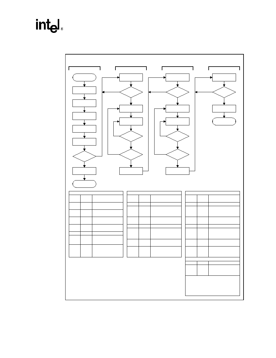
Intel
Æ
Wireless Flash Memory (W18)
Datasheet
33
Figure 7. Enhanced Factory Program Flowchart
EFP Setup
EFP Program
EFP Verify
EFP Exit
1. WA
0
= first Word Address to be programmed within the target block. The BBA (Block Base
Address) must remain constant throughout the program phase data stream; WA can be held
constant at the first address location, or it can be written to sequence up through the addresses
within the block. Writing to a BBA not equal to that of the block currently being written to
terminates the EFP program phase, and instructs the device to enter the EFP verify phase.
2. For proper verification to occur , the verify data stream must be presented to the device in the
same sequence as that of the program phase data stream. Writing to a BBA not equal to WA
terminates the EFP verify phase, and instructs the device to exit EFP .
3. Bits that did not fully program with the single WSM pulse of the EFP program phase receive
additional program-pulse attempts during the EFP verify phase. The device will report any
program failure by setting SR[4]=1; this check can be performed during the full status check after
EFP has been exited for that block, and will indicate any error within the entire data stream.
Comments
Bus
State
Repeat for subsequent operations.
After EFP exit, a Full Status Check can
determine if any program error occurred.
See the Full Status Check procedure in the
Word Program flowchart.
Write
Standby
Read
Write
Write
(note 2)
Read
Standby
Write
Read
Standby
EFP
Setup
Program
Done?
Exit
Program
Phase
Last
Data?
Exit
Verify
Phase
EFP
Exited?
Write
EFP
Confirm
Read
Standby
EFP
Setup
Done?
Read
Standby
Verify
Stream
Ready?
Write
Unlock
Block
Write
(note 1)
Standby
Last
Data?
Standby
(note 3)
Verify
Done?
S
R
[0
]=
1
=
N
Write Data
Address = WA
0
Last
Data?
Write FFFFh
Address
BBA
Program
Done?
Read
Status Register
SR[0]=0=Y
Y
S
R
[0
]=
1
=
N
N
Write Data
Address = WA
0
Verify
Done?
Last
Data?
Read
Status Register
Write FFFFh
Address
BBA
Y
Verify Stream
Ready?
Read
Status Register
SR[7]=0=N
Full Status Check
Procedure
Operation
Complete
Read
Status Register
EFP
Exited?
SR[7]=1=Y
SR[0]=1=N
Start
Write 30h
Address = WA
0
V
PP
= 12V
Unlock Block
Write D0h
Address = WA
0
EFP Setup
Done?
Read
Status Register
SR[7]=1=N
Exit
N
EFP Program
EFP Verify
EFP Exit
EFP Setup
ENHANCED FACTORY PROGRAMMING PROCEDURE
Comments
Bus
State
Data = 30h
Address = WA
0
Data = D0h
Address = WA
0
Status Register
Check SR[7]
0 = EFP ready
1 = EFP not ready
V
PP
= 12V
Unlock block
Check SR[0]
0 = Program done
1 = Program not done
Status Register
Data = FFFFh
Address not within same
BBA
Data = Data to program
Address = WA
0
Device automatically
increments address.
Comments
Bus
State
Data = Word to verify
Address = WA
0
Status Register
Device automatically
increments address.
Data = FFFFh
Address not within same
BBA
Status Register
Check SR[0]
0 = Ready for verify
1 = Not ready for verify
Check SR[0]
0 = Verify done
1 = Verify not done
Status Register
Check SR[7]
0 = Exit not finished
1 = Exit completed
Check V
PP
& Lock
errors (SR[3,1])
Data Stream
Ready?
Read
Status Register
SR[0] =0=Y
S
R
[7
]=
0
=
Y
SR[0]=1=N
Standby
Read
Data
Stream
Ready?
Check SR[0]
0 = Ready for data
1 = Not ready for data
Status Register
SR[0]=0=Y
SR[0] =0=Y
EFP setup time
Standby
EFP setup time
Standby
Error
Condition
Check
If SR[7] = 1:
Check SR[3,1]
SR[3] = 1 = V
PP
error
SR[1] = 1 = locked block

Intel
Æ
Wireless Flash Memory (W18)
34
Datasheet
6.0
Program and Erase Operations
6.1
Program/Erase Suspend and Resume
The Program Suspend and Erase Suspend commands halt an in-progress program or erase
operation. The command can be issued at any device address. The partition corresponding to the
command's address remains in its previous state. A suspend command allows data to be accessed
from memory locations other than the one being programmed or the block being erased.
A program operation can be suspended only to perform a read operation. An erase operation can be
suspended to perform either a program or a read operation within any block, except the block that
is erase suspended. A program command nested within a suspended erase can subsequently be
suspended to read yet another location. Once a program or erase process starts, the Suspend
command requests that the WSM suspend the program or erase sequence at predetermined points
in the algorithm. The partition that is actually suspended continues to output status register data
after the Suspend command is written. An operation is suspended when status bits SR[7] and SR[6]
and/or SR[2] are set.
To read data from blocks within the partition (other than an erase-suspended block), you can write
a Read Array command. Block erase cannot resume until the program operations initiated during
erase suspend are complete. Read Array, Read Status Register, Read Identifier (ID), Read Query,
and Program Resume are valid commands during Program or Erase Suspend. Additionally, Clear
Status Register, Program, Program Suspend, Erase Resume, Lock Block, Unlock Block, and Lock-
Down Block are valid commands during erase suspend.
To read data from a block in a partition that is not programming or erasing, the operation does not
need to be suspended. If the other partition is already in read array, ID, or Query mode, issuing a
valid address returns corresponding data. If the other partition is not in a read mode, one of the read
commands must be issued to the partition before data can be read.
During a suspend, CE# = V
IH
places the device in standby state, which reduces active current. V
PP
must remain at its program level and WP# must remain unchanged while in suspend mode.
A resume command instructs the WSM to continue programming or erasing and clears status
register bits SR[2] (or SR[6]) and SR[7]. The Resume command can be written to any partition.
When read at the partition that is programming or erasing, the device outputs data corresponding to
the partition's last mode. If status register error bits are set, the status register can be cleared before
issuing the next instruction. RST# must remain at V
IH
. See
Figure 8, "Program Suspend / Resume
Flowchart" on page 35
, and
Figure 9, "Erase Suspend / Resume Flowchart" on page 36
.
If a suspended partition was placed in read array, read status register, read identifier (ID), or read
query mode during the suspend, the device remains in that mode and outputs data corresponding to
that mode after the program or erase operation is resumed. After resuming a suspended operation,
issue the read command appropriate to the read operation. To read status after resuming a
suspended operation, issue a Read Status Register command (70h) to return the suspended partition
to status mode.

Intel
Æ
Wireless Flash Memory (W18)
Datasheet
35
Figure 8. Program Suspend / Resume Flowchart
Read Status
Register
SR.7 =
SR.2 =
Write FFh
Susp Partition
Read Array
Data
Program
Completed
Done
Reading
Write FFh
Pgm'd Partition
Write D0h
Any Address
Program
Resumed
Read Array
Data
0
No
0
Yes
1
1
PROGRAM SUSPEND / RESUME PROCEDURE
Write
Program
Resume
Data = D0h
Addr = Suspended block (BA)
Bus
Operation
Command
Comments
Write
Program
Suspend
Data = B0h
Addr = Block to suspend (BA)
Standby
Check SR.7
1 = WSM ready
0 = WSM busy
Standby
Check SR.2
1 = Program suspended
0 = Program completed
Write
Read
Array
Data = FFh
Addr = Any address within the
suspended partition
Read
Read array data from block other than
the one being programmed
Read
Status register data
Toggle CE# or OE# to update Status
register
Addr = Suspended block (BA)
PGM_SUS.WMF
Start
Write B0h
Any Address
Program Suspend
Read
Status
Program
Resume
Read
Array
Read
Array
Write 70h
Same Partition
Write
Read
Status
Data = 70h
Addr = Same partition
If the suspended partition was placed in Read Array mode:
Write
Read
Status
Return partition to Status mode:
Data = 70h
Addr = Same partition
Write 70h
Same Partition
Read
Status

Intel
Æ
Wireless Flash Memory (W18)
36
Datasheet
6.2
Block Erase
The 2-cycle block erase command sequence, consisting of Erase Setup (20h) and Erase Confirm
(D0h), initiates one block erase at the addressed block. Only one partition can be in an erase mode
at a time; other partitions must be in a read mode. The Erase Confirm command internally latches
the address of the block to be erased. Erase forces all bits within the block to 1. SR[7] is cleared
while the erase executes.
Figure 9. Erase Suspend / Resume Flowchart
Erase
Completed
Write FFh
Erased Partition
Read Array
Data
0
0
No
Read
1
Program
Program
Loop
Read Array
Data
1
Yes
Start
Write B0h
Any Address
Read Status
Register
SR.7 =
SR.6 =
Write D0h
Any Address
Erase Resumed
Read or
Program?
Done?
Write
Write
Standby
Standby
Write
Erase
Suspend
Read Array
or Program
Program
Resume
Data = B0h
Addr = Any address
Data = FFh or 40h
Addr = Block to program or read
Check SR.7
1 = WSM ready
0 = WSM busy
Check SR.6
1 = Erase suspended
0 = Erase completed
Data = D0h
Addr = Any address
Bus
Operation
Command
Comments
Read
Status register data. Toggle CE# or
OE# to update Status register
Addr = Same partition
Read or
Write
Read array or program data from/to
block other than the one being erased
ERASE SUSPEND / RESUME PROCEDURE
ERAS_SUS.WMF
Write 70h
Same Partition
Write
Read
Status
Data = 70h
Addr = Same partition
Erase
Resume
Erase
Suspend
Read
Status
Read
Array
Write 70h
Same Partition
Read
Status
If the suspended partition was placed in
Read Array mode or a Program Loop:
Write
Read
Status
Return partition to Status mode:
Data = 70h
Addr = Same partition

Intel
Æ
Wireless Flash Memory (W18)
Datasheet
37
After writing the Erase Confirm command, the selected partition is placed in read status register
mode and reads performed to that partition return the current status data. The address given during
the Erase Confirm command does not need to be the same address used in the Erase Setup
command. So, if the Erase Confirm command is given to partition B, then the selected block in
partition B will be erased even if the Erase Setup command was to partition A.
The 2-cycle erase sequence cannot be interrupted with a bus write operation. For example, an Erase
Setup command must be immediately followed by the Erase Confirm command in order to execute
properly. If a different command is issued between the setup and confirm commands, the partition
is placed in read-status mode, the status register signals a command sequence error, and all
subsequent erase commands to that partition are ignored until the status register is cleared.
The CPU can detect block erase completion by analyzing SR[7] of that partition. If an error bit
(SR[5,3,1]) was flagged, the status register can be cleared by issuing the Clear Status Register
command before attempting the next operation. The partition remains in read-status mode until
another command is written to its CUI. Any CUI instruction can follow after erasing completes.
The CUI can be set to read-array mode to prevent inadvertent status register reads.

Intel
Æ
Wireless Flash Memory (W18)
38
Datasheet
6.3
Read-While-Write and Read-While-Erase
The 1.8 Volt Intel
Æ
Wireless Flash memory supports flexible multi-partition dual-operation
architecture. By dividing the flash memory into many separate partitions, the device can read from
one partition while programing or erasing in another partition; hence the terms, RWW and RWE.
Both of these features greatly enhance data storage performance.
Figure 10. Block Erase Flowchart
SR[3,1] must be cleared before the WSM will allow further
erase attempts.
Only the Clear Status Register command clears SR[5:3,1].
If an error is detected, clear the Status register before
attempting an erase retry or other error recovery.
Start
FULL ERASE STATUS CHECK PROCEDURE
Repeat for subsequent block erasures.
Full status register check can be done after each block erase
or after a sequence of block erasures.
No
Suspend
Erase
1
0
0
0
1
1
1
1
0
Yes
Suspend
Erase
Loop
0
Write 20h
Block Address
Write D0h and
Block Address
Read Status
Register
SR[7] =
Full Erase
Status Check
(if desired)
Block Erase
Complete
Read Status
Register
Block Erase
Successful
SR[1] =
Erase of
Locked Block
Aborted
BLOCK ERASE PROCEDURE
Bus
Operation
Command
Comments
Write
Block
Erase
Setup
Data = 20h
Addr = Block to be erased (BA)
Write
Erase
Confirm
Data = D0h
Addr = Block to be erased (BA)
Read
Read SRD
Toggle CE# or OE# to update SRD
Standby
Check SR[7]
1 = WSM ready
0 = WSM busy
Bus
Operation
Command
Comments
SR[3] =
V
PP
Range
Error
SR[5:4] =
Command
Sequence Error
SR[5] =
Block Erase
Error
Standby
Check SR[3]
1 = V
PP
error
Standby
Check SR[5:4]
Both 1 = Command sequence error
Standby
Check SR[5]
1 = Block erase error
Standby
Check SR[1]
1 = Attempted erase of locked block
Erase aborted

Intel
Æ
Wireless Flash Memory (W18)
Datasheet
39
The product does not support simultaneous program and erase operations. Attempting to perform
operations such as these results in a command sequence error. Only one partition can be
programming or erasing while another partition is reading. However, one partition may be in erase
suspend mode while a second partition is performing a program operation, and yet another partition
is executing a read command.
Table 5, "Command Codes and Descriptions" on page 21
describes
the command codes available for all functions.
7.0
Security Modes
The 1.8 Volt Intel Wireless Flash memory offers both hardware and software security features to
protect the flash data. The software security feature is used by executing the Lock Block command.
The hardware security feature is used by executing the Lock-Down Block command and by
asserting the WP# signal.
Refer to
Figure 11, "Block Locking State Diagram" on page 40
for a state diagram of the flash
security features. Also see
Figure 12, "Locking Operations Flowchart" on page 42
.
7.1
Block Lock Operations
Individual instant block locking protects code and data by allowing any block to be locked or
unlocked with no latency. This locking scheme offers two levels of protection. The first allows
software-only control of block locking (useful for frequently changed data blocks), while the
second requires hardware interaction before locking can be changed (protects infrequently changed
code blocks).
The following sections discuss the locking system operation. The term "state [abc]" specifies
locking states; for example, "state [001]," where a = WP# value, b = block lock-down status bit
D1, and c = Block Lock status register bit D0.
Figure 11, "Block Locking State Diagram" on
page 40
defines possible locking states.
The following summarizes the locking functionality.
∑
All blocks power-up in a locked state.
∑
Unlock commands can unlock these blocks, and lock commands can lock them again.
∑
The Lock-Down command locks a block and prevents it from being unlocked when WP# is
asserted.
-- Locked-down blocks can be unlocked or locked with commands as long as WP# is
deasserted
-- The lock-down status bit is cleared only when the device is reset or powered-down.
Block lock registers are not affected by the V
PP
level. They may be modified and read even if V
PP
V
PPLK
.
Each block's locking status can be set to locked, unlocked, and lock-down, as described in the
following sections. See
Figure 12, "Locking Operations Flowchart" on page 42
.
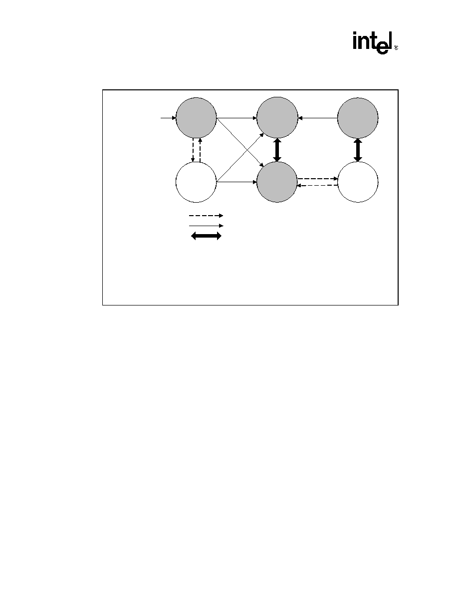
Intel
Æ
Wireless Flash Memory (W18)
40
Datasheet
7.1.1
Lock
All blocks default to locked (state [x01]) after initial power-up or reset. Locked blocks are fully
protected from alteration. Attempted program or erase operations to a locked block will return an
error in SR[1]. Unlocked blocks can be locked by using the Lock Block command sequence.
Similarly, a locked block's status can be changed to unlocked or lock-down using the appropriate
software commands.
7.1.2
Unlock
Unlocked blocks (states [x00] and [110]) can be programmed or erased. All unlocked blocks return
to the locked state when the device is reset or powered-down. An unlocked block's status can be
changed to the locked or locked-down state using the appropriate software commands. A locked
block can be unlocked by writing the Unlock Block command sequence if the block is not locked-
down.
7.1.3
Lock-Down
Locked-down blocks (state [011]) offer the user an additional level of write protection beyond that
of a regular locked block. A block that is locked-down cannot have it's state changed by software if
WP# is asserted. A locked or unlocked block can be locked-down by writing the Lock-Down Block
command sequence. If a block was set to locked-down, then later changed to unlocked, a Lock-
Figure 11. Block Locking State Diagram
[X00]
[X01]
Power-Up/Reset
Unlocked
Locked
[011]
[111]
[110]
Locked-
Down
4,5
Software
Locked
[011]
Hardware
Locked
5
Unlocked
WP# Hardware Control
Notes:
1. [a,b,c] represents [WP#, D1, D0]. X = Don't Care.
2. D1 indicates block Lock-down status. D1 = `0', Lock-down has not been issued to
this block. D1 = `1', Lock-down has been issued to this block.
3. D0 indicates block lock status. D0 = `0', block is unlocked. D0 = `1', block is locked.
4. Locked-down = Hardware + Software locked.
5. [011] states should be tracked by system software to determine difference between
Hardware Locked and Locked-Down states.
Software Block Lock (0x60/0x01) or Software Block Unlock (0x60/0xD0)
Software Block Lock-Down (0x60/0x2F)
WP# hardware control

Intel
Æ
Wireless Flash Memory (W18)
Datasheet
41
Down command should be issued prior asserting WP# will put that block back to the locked-down
state. When WP# is deasserted, locked-down blocks are changed to the locked state and can then
be unlocked by the Unlock Block command.
7.1.4
Block Lock Status
Every block's lock status can be read in read identifier mode. To enter this mode, issue the Read
Identifier command to the device. Subsequent reads at Block Base Address + 02h will output that
block's lock status. For example, to read the block lock status of block 10, the address sent to the
device should be 50002h (for a top-parameter device). The lowest two data bits of the read data, D1
and D0, represent the lock status. D0 indicates the block lock status. It is set by the Lock Block
command and cleared by the Block Unlock command. It is also set when entering the lock-down
state. D1 indicates lock-down status and is set by the Lock-Down command. The lock-down status
bit cannot be cleared by software≠only by device reset or power-down. See
Table 11
.
7.1.5
Lock During Erase Suspend
Block lock configurations can be performed during an erase suspend operation by using the
standard locking command sequences to unlock, lock, or lock-down a block. This feature is useful
when another block requires immediate updating.
To change block locking during an erase operation, first write the Erase Suspend command. After
checking SR[6] to determine the erase operation has suspended, write the desired lock command
sequence to a block; the lock status will be changed. After completing lock, unlock, read, or
program operations, resume the erase operation with the Erase Resume command (D0h).
If a block is locked or locked-down during a suspended erase of the same block, the locking status
bits change immediately. When the erase operation is resumed, it will complete normally.
Locking operations cannot occur during program suspend.
Appendix A, "Write State Machine
States" on page 83
shows valid commands during erase suspend.
7.1.6
Status Register Error Checking
Using nested locking or program command sequences during erase suspend can introduce
ambiguity into status register results.
Because locking changes require 2-cycle command sequences, for example, 60h followed by 01h
to lock a block, following the Configuration Setup command (60h) with an invalid command
produces a command sequence error (SR[5:4]=11b). If a Lock Block command error occurs during
erase suspend, the device sets SR[4] and SR[5] to 1 even after the erase is resumed. When erase is
Table 11. Write Protection Truth Table
VPP
WP#
RST#
Write Protection
X
X
V
IL
Device inaccessible
V
IL
X
V
IH
Word program and block erase prohibited
X
V
IL
V
IH
All lock-down blocks locked
X
V
IH
V
IH
All lock-down blocks can be unlocked

Intel
Æ
Wireless Flash Memory (W18)
42
Datasheet
complete, possible errors during the erase cannot be detected from the status register because of the
previous locking command error. A similar situation occurs if a program operation error is nested
within an erase suspend.
7.1.7
WP# Lock-Down Control
The Write Protect signal, WP#, adds an additional layer of block security. WP# only affects blocks
that once had the Lock-Down command written to them. After the lock-down status bit is set for a
block, asserting WP# forces that block into the lock-down state [011] and prevents it from being
unlocked. After WP# is deasserted, the block's state reverts to locked [111] and software
commands can then unlock the block (for erase or program operations) and subsequently re-lock it.
Only device reset or power-down can clear the lock-down status bit and render WP# ineffective.
7.2
Protection Register
The 1.8 Volt Intel Wireless Flash memory includes a 128-bit protection register. This protection
register is used to increase system security and for identification purposes. The protection register
value can match the flash component to the system's CPU or ASIC to prevent device substitution.
The lower 64 bits within the protection register are programmed by Intel with a unique number in
each flash device. The upper 64 OTP bits within the protection register are left for the customer to
program. Once programmed, the customer segment can be locked to prevent further programming.
Figure 12. Locking Operations Flowchart
No
Opt
i
ona
l
Start
Write 60h
Block Address
Write 90h
BBA + 02h
Read Block Lock
Status
Locking
Change?
Lock Change
Complete
Write 01,D0,2Fh
Block Address
Write FFh
Partition Address
Yes
Write
Write
Write
(Optional)
Read
(Optional)
Standby
(Optional)
Write
Lock
Setup
Lock,
Unlock, or
Lockdown
Confirm
Read ID
Plane
Block Lock
Status
Read
Array
Data = 60h
Addr = Block to lock/unlock/lock-down (BA)
Data = 01h (Lock block)
D0h (Unlock block)
2Fh (Lockdown block)
Addr = Block to lock/unlock/lock-down (BA)
Data = 90h
Addr = BBA + 02h
Block Lock status data
Addr = BBA + 02h
Confirm locking change on DQ[1:0].
(See Block Locking State Transitions Table
for valid combinations.)
Data = FFh
Addr = Any address in same partition
Bus
Operation
Command
Comments
LOCKING OPERATIONS PROCEDURE

Intel
Æ
Wireless Flash Memory (W18)
Datasheet
43
Note:
The individual bits of the user segment of the protection register are OTP, not the register in total.
The user may program each OTP bit individually, one at a time, if desired. After the protection
register is locked, however, the entire user segment is locked and no more user bits can be
programmed.
The protection register shares some of the same internal flash resources as the parameter partition.
Therefore, RWW is only allowed between the protection register and main partitions.
Table 12
describes the operations allowed in the protection register, parameter partition, and main partition
during RWW and RWE.
7.2.1
Reading the Protection Register
Writing the Read Identifier command allows the protection register data to be read 16 bits at a time
from addresses shown in
Table 7, "Device Identification Codes" on page 25
. The protection
register is read from the Read Identifier command and can be read in any partition.Writing the
Read Array command returns the device to read-array mode.
7.2.2
Programing the Protection Register
The Protection Program command should be issued only at the parameter (top or bottom) partition
followed by the data to be programmed at the specified location. It programs the upper 64 bits of
the protection register 16 bits at a time.
Table 7, "Device Identification Codes" on page 25
shows
allowable addresses. See also
Figure 13, "Protection Register Programming Flowchart" on
page 44
. Issuing a Protection Program command outside the register's address space results in a
status register error (SR[4]=1).
Table 12. Simultaneous Operations Allowed with the Protection Register
Protection
Register
Parameter
Partition
Array Data
Main
Partitions
Description
Read
See
Description
Write/Erase
While programming or erasing in a main partition, the protection register can be
read from any other partition. Reading the parameter partition data is not
allowed if the protection register is being read from addresses within the
parameter partition.
See
Description
Read
Write/Erase
While programming or erasing in a main partition, read operations are allowed
in the parameter partition. Accessing the protection registers from parameter
partition addresses is not allowed.
Read
Read
Write/Erase
While programming or erasing in a main partition, read operations are allowed
in the parameter partition. Accessing the protection registers in a partition that
is different from the one being programmed or erased, and also different from
the parameter partition, is allowed.
Write
No Access
Allowed
Read
While programming the protection register, reads are only allowed in the other
main partitions. Access to the parameter partition is not allowed. This is
because programming of the protection register can only occur in the
parameter partition, so it will exist in status mode.
No Access
Allowed
Write/Erase
Read
While programming or erasing the parameter partition, reads of the protection
registers are not allowed in any partition. Reads in other main partitions are
supported.
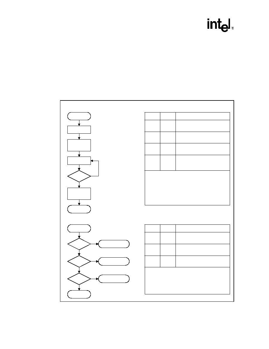
Intel
Æ
Wireless Flash Memory (W18)
44
Datasheet
7.2.3
Locking the Protection Register
PR-LK.0 is programmed to 0 by Intel to protect the unique device number. PR-LK.1 can be
programmed by the user to lock the user portion (upper 64 bits) of the protection register (See
Figure 14, "Protection Register Locking
). This bit is set using the Protection Program command to
program "FFFDh" into PR-LK.
After PR-LK register bits are programmed (locked), the protection register's stored values can't be
changed. Protection Program commands written to a locked section result in a status register error
(SR[4]=1, SR[5]=1).
Figure 13. Protection Register Programming Flowchart
FULL STATUS CHECK PROCEDURE
Protection Program operations addresses must be within the
protection register address space. Addresses outside this
space will return an error.
Repeat for subsequent programming operations.
Full status register check can be done after each program or
after a sequence of program operations.
SR[3] MUST be cleared before the WSM will allow further
program attempts.
Only the Clear Staus Register command clears SR[4:3,1].
If an error is detected, clear the status register before
attempting a program retry or other error recovery.
Yes
No
1,1
1,0
1,1
PROTECTION REGISTER PROGRAMMINGPROCEDURE
Start
Write C0h
Addr=Prot addr
Write Protect.
Register
Address / Data
Read Status
Register
SR[7] = 1?
Full Status
Check
(if desired)
Program
Complete
Read SRD
Program
Successful
SR[4:3] =
SR[4,1] =
SR[4,1] =
V
PP
Range Error
Programming Error
Locked-Register
Program Aborted
Standby
Standby
Bus
Operation
Command
SR[1] SR[3] SR[4]
0
1
1
V
PP
Error
0
0
1
Protection register
program error
Comments
Write
Write
Standby
Protection
Program
Setup
Protection
Program
Data = C0h
Addr = Protection address
Data = Data to program
Addr = Protection address
Check SR[7]
1 = WSM Ready
0 = WSM Busy
Bus
Operation
Command
Comments
Read
Read SRD
Toggle CE# or OE# to update SRD
Standby
1
0
1
Register locked;
Operation aborted
Intel
Æ
Wireless Flash Memory (W18)
Datasheet
45
7.3
VPP Protection
The 1.8 Volt Intel
Æ
Wireless Flash memory provides in-system program and erase at V
PP1
. For
factory programming, it also includes a low-cost, backward-compatible 12 V programming
feature.(
See "Factory Programming" on page 29.
) The EFP feature can also be used to greatly
improve factory program performance as explained in
Section 5.3, "Enhanced Factory Program
(EFP)" on page 30
.
In addition to the flexible block locking, holding the V
PP
programming voltage low can provide
absolute hardware write protection of all flash-device blocks. If V
PP
is below V
PPLK
, program or
erase operations result in an error displayed in SR[3]. (See
Figure 15
.)
NOTE: If the V
CC
supply can sink adequate current, you can use an appropriately valued resistor.
Figure 14. Protection Register Locking
0x84
0x88
0x85
0x81
0x80
PR Lock Register 0
User-Programmable
Intel Factory-Programmed
15 14 13 12 11 10
9
8
7
6
5
4
3
2
1
0
Figure 15. Examples of VPP Power Supply Configurations
∑
12 V fast programming
∑
Absolute write protection with V
PP
V
PPLK
System supply
(Note 1)
VCC
VPP
12 V supply
∑
Low voltage and 12 V fast programming
System supply
12 V supply
∑
Low-voltage programming
∑
Absolute write protection via logic signal
System supply
Prot# (logic signal)
∑
Low-voltage programming
System supply
10K
VCC
VPP
VCC
VPP
VCC
VPP

Intel
Æ
Wireless Flash Memory (W18)
46
Datasheet
8.0
Set Configuration Register
The Set Configuration Register command sets the burst order, frequency configuration, burst
length, and other parameters.
A two-bus cycle command sequence initiates this operation. The configuration register data is
placed on the lower 16 bits of the address bus (A[15:0]) during both bus cycles. The Set
Configuration Register command is written along with the configuration data (on the address bus).
This is followed by a second write that confirms the operation and again presents the configuration
register data on the address bus. The configuration register data is latched on the rising edge of
ADV#, CE#, or WE# (whichever occurs first). This command functions independently of the
applied V
PP
voltage. After executing this command, the device returns to read-array mode. The
configuration register's contents can be examined by writing the Read Identifier command and
then reading location 05h. (See
Table 13
and
Table 14
.)

Intel
Æ
Wireless Flash Memory (W18)
Datasheet
47
Table 13. Configuration Register Definitions
Read
Mode
Res'd
First Access Latency
Count
WAIT
Polarity
Data
Output
Config
WAIT
Config
Burst
Seq
Clock
Config
Res'd
Res'd
Burst
Wrap
Burst Length
RM
R
LC2
LC1
LC0
WT
DOC
WC
BS
CC
R
R
BW
BL2
BL1
BL0
15
14
13
12
11
10
9
8
7
6
5
4
3
2
1
0
Table 14. Configuration Register Descriptions
Bit
Name
Description
Notes
1
15
RM
Read Mode
0 = Synchronous Burst Reads Enabled
1 = Asynchronous Reads Enabled (Default)
2
14
R
Reserved
5
13-11
LC2-0
First Access Latency
Count
001 = Reserved
010 = Code 2
011 = Code 3
100 = Code 4
101 = Code 5
111 = Reserved (Default)
6
10
WT
WAIT Signal Polarity
0 = WAIT signal is asserted low
1 = WAIT signal is asserted high (Default)
3
9
DOC
Data Output Configuration
0 = Hold Data for One Clock
1 = Hold Data for Two Clock (Default)
6
8
WC
WAIT Configuration
0 = WAIT Asserted During Delay
1 = WAIT Asserted One Data Cycle before Delay (Default)
6
7
BS
Burst Sequence
1 = Linear Burst Order (Default)
6
CC
Clock
Configuration
0 = Burst Starts and Data Output on Falling Clock Edge
1 = Burst Starts and Data Output on Rising Clock Edge (Default)
5
R
Reserved
5
4
R
Reserved
5
3
BW
Burst Wrap
0 = Wrap bursts within burst length set by CR[2:0]
1 = Don't wrap accesses within burst length set by CR[2:0].(Default)
2-0
BL2-0
Burst Length
001 = 4-Word Burst
010 = 8-Word Burst
011 = 16-Word Burst
111 = Continuous Burst (Default)
4
NOTES:
1. Undocumented combinations of bits are reserved by Intel for future implementations.
2. Synchronous and page read mode configurations affect reads from main blocks and parameter blocks. Status register and
configuration reads support single read cycles. CR[15]=1 disables configuration set by CR[14:0].
3. Data is not ready when WAIT is asserted.
4. Set the synchronous burst length. In asynchronous page mode, the page size equals four words.
5. Set all reserved configuration register bits to zero.
6. Setting the configuration register for synchronous burst-mode with a latency count of 2 (RCR[13:11] = 010), data hold for 2
clocks (RCR.9 = 1), and WAIT asserted one data cycle before delay (RCR.8 =1) is not supported.
Intel
Æ
Wireless Flash Memory (W18)
48
Datasheet
8.1
Read Mode (CR[15])
All partitions support two high-performance read configurations: synchronous burst mode and
asynchronous page mode (default). CR[15] sets the read configuration to one of these modes.
Status register, query, and identifier modes support only asynchronous and single-synchronous read
operations.
8.2
First Access Latency Count (CR[13:11])
The First Access Latency Count (CR[13:11]) configuration tells the device how many clocks must
elapse from ADV# de-assertion (V
IH
) before the first data word should be driven onto its data pins.
The input clock frequency determines this value. See
Table 13, "Configuration Register
Definitions" on page 47
for latency values.
Figure 16
shows data output latency from ADV#
assertion for different latencies. Refer to
Section 8.2.1, "Latency Count Settings" on page 49
for
Latency Code Settings.
NOTE:
Other First Access Latency Configuration settings are reserved.
)
The 16-word boundary is the end of the device sense word-line.
Figure 16. First Access Latency Configuration
Code 5
Code 4
Code 3
Code 2
Valid
Address
Valid
Output
Valid
Output
Valid
Output
Valid
Output
Valid
Output
Valid
Output
Valid
Output
Valid
Output
Valid
Output
Valid
Output
Valid
Output
Valid
Output
Valid
Output
Valid
Output
Valid
Output
Valid
Output
Valid
Output
Valid
Output
Address [A]
ADV# [V]
CLK [C]
D[15:0] [Q]
D[15:0] [Q]
D[15:0] [Q]
D[15:0] [Q]
Figure 17. Word Boundary
0
1
2
3
4
5
6
7
8
9
A
B
C D
E
F
16 Word Boundary
Word 0 - 3
Word 4 - 7
Word 8 - B
Word C - F
4 Word Boundary
Intel
Æ
Wireless Flash Memory (W18)
Datasheet
49
8.2.1
Latency Count Settings
Table 15. Latency Count Settings for V
CCQ
= 1.35 V - 1.8 V (.13 µm lithography)
V
CCQ
= 1.35 V - 1.8 V
Unit
t
AVQV
/t
CHQV
(65ns/14ns)
t
AVQV
/t
CHQV
(85ns/20ns)
Latency Count
Settings
2
3, 4, 5
2
3, 4, 5
Frequency
< 39
< 54
< 30
< 40
MHz
Table 16. Latency Count Setting for V
CCQ
= 1.7 V - 2.24 V (.13 µm lithography)
V
CCQ
= 1.7 - 2.24 V
Unit
t
AVQV
/t
CHQV
(60ns/11ns)
t
AVQV
/t
CHQV
(80ns/14ns)
Latency Count
Settings
2
3
4, 5
2
3
4, 5
Frequency
Support
< 40
< 61
< 66
< 30
< 45
< 54
MHz
Table 17. Latency Count Setting for V
CCQ
= 1.7 V - 2.24 V (.18 µm lithography)
V
CCQ
= 1.7 - 2.24 V
Unit
t
AVQV
/t
CHQV
(70ns/14ns)
t
AVQV
/t
CHQV
(85ns/18ns)
Latency Count
Settings
2
3, 4, 5
2
3, 4, 5
Frequency
Support
< 35
<52
< 29
< 40
MHz

Intel
Æ
Wireless Flash Memory (W18)
50
Datasheet
8.3
WAIT Signal Polarity (CR[10])
If the WT bit is cleared (CR[10]=0), then WAIT is configured to be asserted low. This means that a
0 on the WAIT signal indicates that data is not ready and the data bus contains invalid data.
Conversely, if CR[10] is set, then WAIT is asserted high. In either case, if WAIT is deasserted, then
data is ready and valid. WAIT is asserted during asynchronous page mode reads.
8.4
WAIT Signal Function
The WAIT signal indicates data valid when the device is operating in synchronous mode
(CR[15]=0), and when addressing a partition that is currently in read-array mode. The WAIT signal
is only "deasserted" when data is valid on the bus.
When the device is operating in synchronous non-read-array mode, such as read status, read ID, or
read query, WAIT is set to an "asserted" state as determined by CR[10]. See
Figure 26, "WAIT
Signal in Synchronous Non-Read Array Operation Waveform" on page 72
.
When the device is operating in asynchronous page mode or asynchronous single word read mode,
WAIT is set to an "asserted" state as determined by CR[10]. See
Figure 22, "Page-Mode Read
Operation Waveform" on page 68
, and
Figure 20, "Asynchronous Read Operation Waveform" on
page 66
.
From a system perspective, the WAIT signal is in the asserted state (based on CR[10]) when the
device is operating in synchronous non-read-array mode (such as Read ID, Read Query, or Read
Status), or if the device is operating in asynchronous mode (CR[15]=1). In these cases, the system
software should ignore (mask) the WAIT signal, because it does not convey any useful information
about the validity of what is appearing on the data bus.
Figure 18. Example: Latency Count Setting at 3
A
MAX-0
(A)
DQ
15-0
(D/Q)
CLK (C)
CE# (E)
ADV# (V)
R103
Valid
Output
Valid
Output
High Z
t
ADD-DELAY
t
DATA
1nd
0st
2rd
3th
4th
Valid Address
Code 3

Intel
Æ
Wireless Flash Memory (W18)
Datasheet
51
8.5
Data Hold (CR[9])
The Data Output Configuration bit (CR[9]) determines whether a data word remains valid on the
data bus for one or two clock cycles. The processor's minimum data set-up time and the flash
memory's clock-to-data output delay determine whether one or two clocks are needed.
A Data Output Configuration set at 1-clock data hold corresponds to a 1-clock data cycle; a Data
Output Configuration set at 2-clock data hold corresponds to a 2-clock data cycle. The setting of
this configuration bit depends on the system and CPU characteristics. For clarification, see
Figure
19, "Data Output Configuration with WAIT Signal Delay" on page 52
.
A method for determining this configuration setting is shown below.
To set the device at 1-clock data hold for subsequent reads, the following condition must be
satisfied:
t
CHQV (ns) +
t
DATA
(ns)
One CLK Period (ns)
As an example, use a clock frequency of 66 MHz and a clock period of 15 ns. Assume the data
output hold time is one clock. Apply this data to the formula above for the subsequent reads:
11 ns + 4 ns
15 ns
This equation is satisfied, and data output will be available and valid at every clock period. If t
DATA
is long, hold for two cycles.
During page-mode reads, the initial access time can be determined by the formula:
t
ADD-DELAY (ns) +
t
DATA
(ns)
+
t
AVQV
(ns)
Subsequent reads in page mode are defined by:
t
APA (ns) +
t
DATA
(ns)
(minimum time)
Table 18. WAIT Signal Conditions
CONDITION
WAIT
CE# = V
IH
CE# = V
IL
Tri-State
Active
OE#
No-Effect
Synchronous Array Read
Active
Synchronous Non-Array Read
Asserted
All Asynchronous Read and all Write
Asserted

Intel
Æ
Wireless Flash Memory (W18)
52
Datasheet
NOTE:
WAIT shown asserted high (CR[10]=1).
8.6
WAIT Delay (CR[8])
The WAIT configuration bit (CR[8]) controls WAIT signal delay behavior for all synchronous
read-array modes. Its setting depends on the system and CPU characteristics. The WAIT can be
asserted either during, or one data cycle before, a valid output.
In synchronous linear read array (no-wrap mode CR[3]=1) of 4-, 8-, 16-, or continuous-word burst
mode, an output delay may occur when a burst sequence crosses its first device-row boundary (16-
word boundary). If the burst start address is 4-word boundary aligned, the delay does not occur. If
the start address is misaligned to a 4-word boundary, the delay occurs once per burst-mode read
sequence. The WAIT signal informs the system of this delay.
8.7
Burst Sequence (CR[7])
The burst sequence specifies the synchronous-burst mode data order (see
Table 19, "Sequence and
Burst Length" on page 53
). When operating in a linear burst mode, either 4-, 8-, or 16-word burst
length with the burst wrap bit (CR[3]) set, or in continuous burst mode, the device may incur an
output delay when the burst sequence crosses the first 16-word boundary. (See
Figure 17, "Word
Boundary" on page 48
for word boundary description.) This depends on the starting address. If the
starting address is aligned to a 4-word boundary, there is no delay. If the starting address is the end
of a 4-word boundary, the output delay is one clock cycle less than the First Access Latency Count;
this is the worst-case delay. The delay takes place only once, and only if the burst sequence crosses
a 16-word boundary. The WAIT pin informs the system of this delay. For timing diagrams of WAIT
functionality, see these figures:
∑
Figure 23, "Single Synchronous Read-Array Operation Waveform" on page 69
∑
Figure 24, "Synchronous 4-Word Burst Read Operation Waveform" on page 70
∑
Figure 25, "WAIT Functionality for EOWL (End-of-Word Line) Condition Waveform" on
page 71
Figure 19. Data Output Configuration with WAIT Signal Delay
DQ
15-0
[Q]
CLK [C]
Valid
Output
Valid
Output
Valid
Output
DQ
15-0
[Q]
Valid
Output
1 CLK
Data Hold
WAIT (CR.8 = 1)
WAIT (CR.8 = 0)
t
CHQV
t
CHQV
WAIT (CR.8 = 0)
WAIT (CR.8 = 1)
2 CLK
Data Hold
t
CHTL/H
Note 1
Note 1
Note 1
Note 1
Valid
Output

Intel
Æ
Wireless Flash Memory (W18)
Datasheet
53
Table 19. Sequence and Burst Length
Start
Addr.
(Dec)
Burst Addressing Sequence (Decimal)
4-Word
Burst
CR[2:0]=0
01b
8-Word Burst
CR[2:0]=010b
16-Word Burst
CR[2:0]=011b
Continuous
Burst
CR[2:0]=111b
Linear
Linear
Linear
Linear
W
r
ap
(
C
R
[
3]
=
0
)
0
0-1-2-3
0-1-2-3-4-5-6-7
0-1-2...14-15
0-1-2-3-4-5-6-...
1
1-2-3-0
1-2-3-4-5-6-7-0
1-2-3...14-15-0
1-2-3-4-5-6-7-...
2
2-3-0-1
2-3-4-5-6-7-0-1
2-3-4...15-0-1
2-3-4-5-6-7-8-...
3
3-0-1-2
3-4-5-6-7-0-1-2
3-4-5...15-0-1-2
3-4-5-6-7-8-9-...
4
4-5-6-7-0-1-2-3
4-5-6...15-0-1-2-
3
4-5-6-7-8-9-10...
5
5-6-7-0-1-2-3-4
5-6-7...15-0-1...4
5-6-7-8-9-10-11...
6
6-7-0-1-2-3-4-5
6-7-8...15-0-1...5
6-7-8-9-10-11-12-
...
7
7-0-1-2-3-4-5-6
7-8-9...15-0-1...6
7-8-9-10-11-12-
13...
...
...
...
..
.
...
14
14-15-0-1...13
14-15-16-17-18-19-
20-...
15
15-0-1-2-3...14
15-16-17-18-19-...
N
o
-W
ra
p
(
CR[3
]
=1
)
0
0-1-2-3
0-1-2-3-4-5-6-7
0-1-2...14-15
0-1-2-3-4-5-6-...
1
1-2-3-4
1-2-3-4-5-6-7-8
1-2-3...15-16
1-2-3-4-5-6-7-...
2
2-3-4-5
2-3-4-5-6-7-8-9
2-3-4...16-17
2-3-4-5-6-7-8-...
3
3-4-5-6
3-4-5-6-7-8-9-
10
3-4-5...17-18
3-4-5-6-7-8-9-...
4
4-5-6-7-8-9-10-
11
4-5-6...18-19
4-5-6-7-8-9-10...
5
5-6-7-8-9-10-
11-12
5-6-7...19-20
5-6-7-8-9-10-11...
6
6-7-8-9-10-11-
12-13
6-7-8...20-21
6-7-8-9-10-11-12-
...
7
7-8-9-10-11-
12-13-14
7-8-9...21-22
7-8-9-10-11-12-
13...
..
.
..
.
..
.
..
.
..
.
14
14-15...28-29
14-15-16-17-18-
19-20-...
15
15-16...29-30
15-16-17-18-19-
20-21-...

Intel
Æ
Wireless Flash Memory (W18)
54
Datasheet
8.8
Clock Edge (CR[6])
Configuring the valid clock edge enables a flexible memory interface to a wide range of burst
CPUs. Clock configuration sets the device to start a burst cycle, output data, and assert WAIT on
the clock's rising or falling edge.
8.9
Burst Wrap (CR[3])
The burst wrap bit determines whether 4-, 8-, or 16-word burst accesses wrap within the burst-
length boundary or whether they cross word-length boundaries to perform linear accesses. No-
wrap mode (CR[3]=1) enables WAIT to hold off the system processor, as it does in the continuous
burst mode, until valid data is available. In no-wrap mode (CR[3]=0), the device operates similarly
to continuous linear burst mode but consumes less power during 4-, 8-, or 16-word bursts.
For example, if CR[3]=0 (wrap mode) and CR[2:0] = 1h (4-word burst), possible linear burst
sequences are 0-1-2-3, 1-2-3-0, 2-3-0-1, 3-0-1-2.
If CR[3]=1 (no-wrap mode) and CR[2:0] = 1h (4-word burst length), then possible linear burst
sequences are 0-1-2-3, 1-2-3-4, 2-3-4-5, and 3-4-5-6. CR[3]=1 not only enables limited non-
aligned sequential bursts, but also reduces power by minimizing the number of internal read
operations.
Setting CR[2:0] bits for continuous linear burst mode (7h) also achieves the above 4-word burst
sequences. However, significantly more power may be consumed. The 1-2-3-4 sequence, for
example, consumes power during the initial access, again during the internal pipeline lookup as the
processor reads word 2, and possibly again, depending on system timing, near the end of the
sequence as the device pipelines the next 4-word sequence. CR[3]=1 while in 4-word burst mode
(no-wrap mode) reduces this excess power consumption.
8.10
Burst Length (CR[2:0])
The Burst Length bit (BL[2:0]) selects the number of words the device outputs in synchronous read
access of the flash memory array. The burst lengths are 4-word, 8-word, 16-word, and continuous
word.
Continuous-burst accesses are linear only, and do not wrap within any word length boundaries (see
Table 19, "Sequence and Burst Length" on page 53
). When a burst cycle begins, the device outputs
synchronous burst data until it reaches the end of the "burstable" address space.

Intel
Æ
Wireless Flash Memory (W18)
Datasheet
55
9.0
Power Consumption
1.8 Volt Intel
Æ
Wireless Flash memory devices have a layered approach to power savings that can
significantly reduce overall system power consumption. The APS feature reduces power
consumption when the device is selected but idle. If CE# is deasserted, the memory enters its
standby mode, where current consumption is even lower. Asserting RST# provides current savings
similar to standby mode. The combination of these features can minimize memory power
consumption, and therefore, overall system power consumption.
9.1
Active Power
With CE# at V
IL
and RST# at V
IH
, the device is in the active mode. Refer to
Section 10.3, "DC
Current Characteristics (.13 µm and .18 µm)" on page 58
, for I
CC
values. When the device is in
"active" state, it consumes the most power from the system. Minimizing device active current
therefore reduces system power consumption, especially in battery-powered applications.
9.2
Automatic Power Savings (APS)
Automatic Power Saving (APS) provides low-power operation during a read's active state. During
APS mode, I
CCAPS
is the average current measured over any 5 ms time interval 5 µs after the
following events happen:
∑
There is no internal sense activity;
∑
CE# is asserted;
∑
The address lines are quiescent, and at V
SSQ
or V
CCQ
.
OE# may be asserted during APS.
9.3
Standby Power
With CE# at V
IH
and the device in read mode, the flash memory is in standby mode, which disables
most device circuitry and substantially reduces power consumption. Outputs are placed in a high-
impedance state independent of the OE# signal state. If CE# transitions to V
IH
during erase or
program operations, the device continues the operation and consumes corresponding active power
until the operation is complete. ICCS is the average current measured over any 5 ms time interval 5
µs after a CE# de-assertion.
9.4
Power-Up/Down Characteristics
The device is protected against accidental block erasure or programming during power transitions.
Power supply sequencing is not required if V
CC
, V
CCQ
, and V
PP
are connected together; so it
doesn't matter whether V
PP
or V
CC
powers-up first. If V
CCQ
and/or V
PP
are not connected to the
system supply, then V
CC
should attain V
CCMIN
before applying VCCQ and VPP. Device inputs
should not be driven before supply voltage = V
CCMIN.
Power supply transitions should only occur
when RST# is low.

Intel
Æ
Wireless Flash Memory (W18)
56
Datasheet
9.4.1
System Reset and RST#
The use of RST# during system reset is important with automated program/erase devices because
the system expects to read from the flash memory when it comes out of reset. If a CPU reset occurs
without a flash memory reset, proper CPU initialization will not occur because the flash memory
may be providing status information instead of array data. To allow proper CPU/flash initialization
at system reset, connect RST# to the system CPU RESET# signal.
System designers must guard against spurious writes when VCC voltages are above V
LKO
.
Because both WE# and CE# must be low for a command write, driving either signal to V
IH
inhibits
writes to the device. The CUI architecture provides additional protection because alteration of
memory contents can only occur after successful completion of the two-step command sequences.
The device is also disabled until RST# is brought to V
IH
, regardless of its control input states. By
holding the device in reset (RST# connected to system PowerGood) during power-up/down,
invalid bus conditions during power-up can be masked, providing yet another level of memory
protection.
9.4.2
VCC, VPP, and RST# Transitions
The CUI latches commands issued by system software and is not altered by VPP or CE# transitions
or WSM actions. Read-array mode is its power-up default state after exit from reset mode or after
VCC transitions above V
LKO
(Lockout voltage).
After completing program or block erase operations (even after VPP transitions below V
PPLK
), the
Read Array command must reset the CUI to read-array mode if flash memory array access is
desired.
9.5
Power Supply Decoupling
When the device is accessed, many internal conditions change. Circuits are enabled to charge
pumps and switch voltages. This internal activity produces transient noise. To minimize the effect
of this transient noise, device decoupling capacitors are required. Transient current magnitudes
depend on the device outputs' capacitive and inductive loading. Two-line control and proper
decoupling capacitor selection suppresses these transient voltage peaks. Each flash device should
have a 0.1 µF ceramic capacitor connected between each power (VCC, VCCQ, VPP)
,
and ground
(VSS, VSSQ) signal. High-frequency, inherently low-inductance capacitors should be as close as
possible to package signals.

Intel
Æ
Wireless Flash Memory (W18)
Datasheet
57
10.0
Thermal and DC Characteristics
10.1
Absolute Maximum Ratings
Warning:
Stressing the device beyond the "Absolute Maximum Ratings" may cause permanent damage.
These are stress ratings only. Operation beyond the "Operating Conditions" is not recommended,
and extended exposure beyond the "Operating Conditions" may affect device reliability.
10.2
Operating Conditions
Notice:
This datasheet contains information on products in the design phase of development. The information
here is subject to change without notice. Do not finalize a design with this information.
Table 20. Absolute Maximum Ratings
Parameter
Note
Maximum Rating
Temperature under Bias
≠40 ∞C to +85 ∞C
Storage Temperature
≠65 ∞C to +125 ∞C
Voltage on Any Pin (except VCC, VCCQ, VPP)
≠0.5 V to +2.45 V
VPP Voltage
1,2,3
≠0.2 V to +14 V
VCC and VCCQ Voltage
1
≠0.2 V to +2.45 V
Output Short Circuit Current
4
100 mA
NOTES:
1. All specified voltages are relative to VSS. Minimum DC voltage is ≠0.5 V on input/output pins and
≠0.2 V on VCC and VPP pins. During transitions, this level may undershoot to ≠2.0 V for periods < 20
ns which, during transitions, may overshoot to V
CC
+2.0 V for periods < 20 ns.
2. Maximum DC voltage on VPP may overshoot to +14.0 V for periods < 20 ns.
3. V
PP
program voltage is normally V
PP1
. V
PP
can be 12 V ± 0.6 V for 1000 cycles on the main blocks
and 2500 cycles on the parameter blocks during program/erase.
4. Output shorted for no more than one second. No more than one output shorted at a time.
Table 21. Extended Temperature Operation (Sheet 1 of 2)
Symbol
Parameter
1
Note
Min
Nom
Max
Unit
T
A
Operating Temperature
≠40
25
85
∞C
V
CC
V
CC
Supply Voltage
3
1.7
1.8
1.95
V
V
CCQ
I/O Supply Voltage
3
1.7
1.8
2.24
I/O Supply Voltage (Extended)
4
1.35
1.5
1.8
V
PP1
V
PP
Voltage Supply (Logic Level)
2
0.90
1.80
1.95
V
PP2
Factory Programming V
PP
2
11.4
12.0
12.6
t
PPH
Maximum V
PP
Hours
V
PP
= 12 V
2
80
Hours

Intel
Æ
Wireless Flash Memory (W18)
58
Datasheet
10.3
DC Current Characteristics (.13 µm and .18 µm)
Block
Erase
Cycles
Main and Parameter
Blocks
V
PP
V
CC
2
100,000
Cycles
Main Blocks
V
PP
= 12 V
2
1000
Parameter Blocks
V
PP
= 12 V
2
2500
NOTES:
1. See
Section 10.3
and
Section 10.4, "DC Voltage Characteristics" on page 60
for specific voltage-range
specifications.
2. VPP is normally V
PP1
. VPP can be connected to 11.4 V≠12.6 V for 1000 cycles on main blocks for
extended temperatures and 2500 cycles on parameter blocks at extended temperature.
3. Contact your Intel field representative for V
CC
/V
CCQ
operations down to 1.65 V.
4. See the tables in
Section 10.0, "Thermal and DC Characteristics" on page 57
and in
Section 11.0, "AC
Characteristics" on page 62
for operating characteristics within the Extended-V
CCQ
voltage range.
Table 22. DC Current Characteristics (Sheet 1 of 3)
Sym
Parameter
(1)
Note
V
CCQ
=1.35 V ≠
1.8 V
V
CCQ
= 1.8 V
Unit
Test Condition
32/64/128 Mbit
32/64 Mbit
128 Mbit
Typ
Max
Typ
Max
Typ
Max
I
LI
Input Load
9
TBD
±1
±1
µA
V
CC
= V
CC
Max
V
CCQ
= V
CCQ
Max
V
IN
= V
CCQ
or GND
I
LO
Output
Leakage
DQ[15:0]
TBD
±1
±1
µA
V
CC
= V
CC
Max
V
CCQ
= V
CCQ
Max
V
IN
= V
CCQ
or GND
.18 µm
I
CCS
V
CC
Standby
10
TBD
TBD
5
18
5
25
µA
V
CC
= V
CC
Max
V
CCQ
= V
CCQ
Max
CE# = V
CC
RST# =V
SSQ
.13 µm
I
CCS
TBD
TBD
8
50
8
70
.18 µm
I
CCAPS
APS
11
TBD
TBD
5
18
5
25
µA
V
CC
= V
CC
Max
V
CCQ
= V
CCQ
Max
CE# = V
SSQ
RST# =V
CCQ
All other inputs =V
CCQ
or
V
SSQ
.13 µm
I
CCAPS
TBD
TBD
8
50
8
70
Table 21. Extended Temperature Operation (Sheet 2 of 2)
Symbol
Parameter
1
Note
Min
Nom
Max
Unit

Intel
Æ
Wireless Flash Memory (W18)
Datasheet
59
I
CCR
Average
V
CC
Read
Asynchronous
Page Mode
f=13 MHz
2
TBD
TBD
3
6
4
7
mA
4 Word Read
V
CC
=
V
CC
Max
CE# = V
IL
OE# = V
IH
Inputs = V
IH
or V
IL
Synchronous
CLK = 40 MHz
2
TBD
TBD
6
13
6
13
mA
Burst length
= 4
TBD
TBD
8
14
8
14
mA
Burst length
= 8
TBD
TBD
10
18
11
19
mA
Burst length
=16
TBD
TBD
11
20
11
20
mA
Burst length
= Continuous
Synchronous
CLK = 54 MHz
2
TBD
TBD
7
16
7
16
mA
Burst length
= 4
TBD
TBD
10
18
10
18
mA
Burst length
= 8
TBD
TBD
12
22
12
22
mA
Burst length
= 16
TBD
TBD
13
25
13
25
mA
Burst length
= Continuous
I
CCR
Average
V
CC
Read
Synchronous
CLK = 66 MHz
2, 3
TBD
TBD
8
17
N.A.
N.A.
mA
Burst length
= 4
V
CC
=
V
CC
Max
CE# = V
IL
OE# = V
IH
Inputs = V
IH
or V
IL
TBD
TBD
11
20
N.A.
N.A.
mA
Burst length
= 8
TBD
TBD
14
25
N.A.
N.A.
mA
Burst length
= 16
TBD
TBD
16
30
N.A.
N.A.
mA
Burst length
= Continuous
I
CCW
V
CC
Program
3,4,5
TBD
TBD
18
40
18
40
mA
V
PP
= V
PP1,
Program in
Progress
TBD
TBD
8
15
8
15
mA
V
PP
= V
PP2,
Program in
Progress
I
CCE
V
CC
Block Erase
3,4,5
TBD
TBD
18
40
18
40
mA
V
PP
= V
PP1,
Block Erase in
Progress
TBD
TBD
8
15
8
15
mA
V
PP
= V
PP2,
Block Erase in
Progress
I
CCWS
V
CC
Program Suspend
6
TBD
TBD
5
18
5
25
µA
CE# = V
CC,
Program Sus-
pended
I
CCES
V
CC
Erase Suspend
6
TBD
TBD
5
18
5
25
µA
CE# = V
CC,
Erase Sus-
pended
Table 22. DC Current Characteristics (Sheet 2 of 3)
Sym
Parameter
(1)
Note
V
CCQ
=1.35 V ≠
1.8 V
V
CCQ
= 1.8 V
Unit
Test Condition
32/64/128 Mbit
32/64 Mbit
128 Mbit
Typ
Max
Typ
Max
Typ
Max
Intel
Æ
Wireless Flash Memory (W18)
60
Datasheet
10.4
DC Voltage Characteristics
I
PPS
(I
PPWS
,
I
PPES
)
V
PP
Standby
V
PP
Program Suspend
V
PP
Erase Suspend
3
TBD
TBD
0.2
5
0.2
5
µA
V
PP
<
V
CC
I
PPR
V
PP
Read
TBD
TBD
2
15
2
15
µA
V
PP
V
CC
I
PPW
V
PP
Program
4
TBD
TBD
0.05
0.10
0.05
0.10
mA
V
PP
= V
PP1,
Program in
Progress
TBD
TBD
8
22
16
37
V
PP
= V
PP2,
Program in
Progress
I
PPE
V
PP
Erase
4
TBD
TBD
0.05
0.10
0.05
0.10
mA
V
PP
= V
PP1,
Erase in
Progress
TBD
TBD
8
22
8
22
V
PP
= V
PP2,
Erase in
Progress
NOTES:
1. All currents are RMS unless noted. Typical values at typical V
CC
, T
A
= +25∞C.
2. Automatic Power Savings (APS) reduces I
CCR
to approximately standby levels in static operation. See I
CCRQ
specification
for details.
3. Sampled, not 100% tested.
4. V
CC
read + program current is the sum of V
CC
read and V
CC
program currents.
5. V
CC
read + erase current is the sum of V
CC
read and V
CC
erase currents.
6. I
CCES
is specified with device deselected. If device is read while in erase suspend, current is I
CCES
plus I
CCR
.
7. V
PP
<
= V
PPLK
inhibits erase and program operations. Don't use V
PPL
and V
PPH
outside their valid ranges.
8. V
IL
can undershoot to ≠0.4V and V
IH
can overshoot to V
CCQ
+0.4V for durations of 20 ns or less.
9. If V
IN
>V
CC
the input load current increases to 10 µA max.
10.ICCS is the average current measured over any 5ms time interval 5
µ
s after a CE# de-assertion.
11.Refer to section
Section 9.2, "Automatic Power Savings (APS)" on page 55
for I
CCAPS
measurement details.
12.TBD values are to be determined pending silicon characterization.
Table 23. DC Voltage Characteristics (Sheet 1 of 2)
Sym
Parameter
(1)
Note
V
CCQ
=1.35 V ≠ 1.8 V
V
CCQ
= 1.8 V
Unit
Test Condition
32/64/128 Mbit
32/64 Mbit
128 Mbit
Min
Max
Min
Max
Min
Max
V
IL
Input Low
8
0
0.2
0
0.4
0
0.4
V
V
IH
Input High
V
CCQ
≠ 0.2
V
CCQ
V
CCQ
≠ 0.4
V
CCQ
V
CCQ
≠ 0.4
V
CCQ
V
V
OL
Output Low
0.1
0.1
0.1
V
V
CC
= V
CC
Min
V
CCQ
= V
CCQ
Min
I
OL
= 100 µA
Table 22. DC Current Characteristics (Sheet 3 of 3)
Sym
Parameter
(1)
Note
V
CCQ
=1.35 V ≠
1.8 V
V
CCQ
= 1.8 V
Unit
Test Condition
32/64/128 Mbit
32/64 Mbit
128 Mbit
Typ
Max
Typ
Max
Typ
Max
Intel
Æ
Wireless Flash Memory (W18)
Datasheet
61
V
OH
Output High
V
CCQ
≠ 0.1
V
CCQ
≠ 0.1
V
CCQ
≠ 0.1
V
V
CC
= V
CC
Min
V
CCQ
= V
CCQ
Min
I
OH
= ≠100 µA
V
PPLK
V
PP
Lock-Out
7
0.4
0.4
0.4
V
V
LKO
V
CC
Lock
1.0
1.0
1.0
V
V
ILKOQ
V
CCQ
Lock
TBD
0.9
0.9
V
NOTE:
For all numbered note references in this table, refer to the notes in
Table 22, "DC Current Characteristics" on page 58
.
Table 23. DC Voltage Characteristics (Sheet 2 of 2)
Sym
Parameter
(1)
Note
V
CCQ
=1.35 V ≠ 1.8 V
V
CCQ
= 1.8 V
Unit
Test Condition
32/64/128 Mbit
32/64 Mbit
128 Mbit
Min
Max
Min
Max
Min
Max
Intel
Æ
Wireless Flash Memory (W18)
62
Datasheet
11.0
AC Characteristics
11.1
Read Operations ≠ .13
µ
m Lithography
Table 24. Read Operations-- .13
µ
m Lithography (Sheet 1 of 2)
#
Sym
Parameter
1,2
Notes
V
CCQ
=
1.35 V ≠ 1.8 V
V
CCQ
=
1.7 V ≠ 2.24 V
Unit
-65
-85
-60
-80
Min
Max
Min
Max
Min
Max
Min
Max
Asynchronous Specifications
R1
t
AVAV
Read Cycle Time
7,8
65
85
60
80
ns
R2
t
AVQV
Address to Output Valid
7,8
65
85
60
80
ns
R3
t
ELQV
CE# Low to Output Valid
7,8
65
85
60
80
ns
R4
t
GLQV
OE# Low to Output Valid
4
25
30
20
25
ns
R5
t
PHQV
RST# High to Output Valid
150
150
150
150
ns
R6
t
ELQX
CE# Low to Output Low-Z
5
0
0
0
0
ns
R7
t
GLQX
OE# Low to Output Low-Z
4,5
0
0
0
0
ns
R8
t
EHQZ
CE# High to Output High-Z
5
17
20
14
17
ns
R9
t
GHQZ
OE# High to Output High-Z
4,5
14
14
14
14
ns
R10
t
OH
CE# (OE#) High to Output Low-Z
4,5
0
0
0
0
ns
Latching Specifications
R101
t
AVVH
Address Setup to ADV# High
7
7
7
7
ns
R102
t
ELVH
CE# Low to ADV# High
10
10
10
10
ns
R103
t
VLQV
ADV# Low to Output Valid
7,8
65
85
60
80
ns
R104
t
VLVH
ADV# Pulse Width Low
7
7
7
7
ns
R105
t
VHVL
ADV# Pulse Width High
7
7
7
7
ns
R106
t
VHAX
Address Hold from ADV# High
3
7
7
7
7
ns
R108
t
APA
Page Address Access Time
25
30
20
25
ns
Clock Specifications
R200
f
CLK
CLK Frequency
54
40
66
54
MHz
R201
t
CLK
CLK Period
18.5
25
15
18.5
ns
R202
t
CH/L
CLK High or Low Time
4.5
9.5
3.5
4.5
ns
R203
t
CHCL
CLK Fall or Rise Time
3
3
3
3
ns
Intel
Æ
Wireless Flash Memory (W18)
Datasheet
63
Synchronous Specifications
R301
t
AVCH
Address Valid Setup to CLK
7
7
7
7
ns
R302
t
VLCH
ADV# Low Setup to CLK
7
7
7
7
ns
R303
t
ELCH
CE# Low Setup to CLK
7
7
7
7
ns
R304
t
CHQV
CLK to Output Valid
8
14
20
11
14
ns
R305
t
CHQX
Output Hold from CLK
3
3
3
3
ns
R306
t
CHAX
Address Hold from CLK
3
7
7
7
7
ns
R307
t
CHTV
CLK to WAIT Valid
8
14
20
11
14
ns
R308
t
ELTV
CE# Low to WAIT Valid
6
14
20
11
14
ns
R309
t
EHTZ
CE# High to WAIT High-Z
5,6
14
20
11
14
ns
R310
t
EHEL
CE# Pulse Width High
6
14
14
14
14
ns
Table 24. Read Operations-- .13
µ
m Lithography (Sheet 2 of 2)
#
Sym
Parameter
1,2
Notes
V
CCQ
=
1.35 V ≠ 1.8 V
V
CCQ
=
1.7 V ≠ 2.24 V
Unit
-65
-85
-60
-80
Min
Max
Min
Max
Min
Max
Min
Max
Intel
Æ
Wireless Flash Memory (W18)
64
Datasheet
11.2
Read Operations ≠ .18
µ
m Lithography
Table 25. Read Operations -- .18
µ
m Lithography (Sheet 1 of 2)
#
Sym
Parameter
(1,2)
Notes
32/64 Mbit
128 Mbit
Unit
≠70
≠85
-85
Min
Max
Min
Max
Min
Max
Asynchronous Specifications
R1
t
AVAV
Read Cycle Time
70
85
85
ns
R2
t
AVQV
Address to Output Delay
70
85
85
ns
R3
t
ELQV
CE# Low to Output Delay
70
85
85
ns
R4
t
GLQV
OE# Low to Output Delay
4
30
30
30
ns
R5
t
PHQV
RST# High to Output Delay
150
150
150
ns
R6
t
ELQX
CE# Low to Output in Low-Z
5
0
0
0
ns
R7
t
GLQX
OE# Low to Output in Low-Z
4,5
0
0
0
ns
R8
t
EHQZ
CE# High to Output in High-Z
5
20
20
20
ns
R9
t
GHQZ
OE# High to Output in High-Z
4,5
14
14
14
ns
R10
t
OH
CE# (OE#) High to Output in Low-Z
4,5
0
0
0
ns
Latching Specifications
R101
t
AVVH
Address Setup to ADV# High
10
10
10
ns
R102
t
ELVH
CE# Low to ADV# High
10
10
10
ns
R103
t
VLQV
ADV# Low to Output Delay
70
85
85
ns
R104
t
VLVH
ADV# Pulse Width Low
10
10
10
ns
R105
t
VHVL
ADV# Pulse Width High
10
10
10
ns
R106
t
VHAX
Address Hold from ADV# High
3
9
9
9
ns
R108
t
APA
Page Address Access Time
20
25
25
ns
Clock Specifications
R200
f
CLK
CLK Frequency
52
40
40
MHz
R201
t
CLK
CLK Period
19
25
25
ns
R202
t
CH/L
CLK High or Low Time
5
5
5
ns
R203
t
CHCL
CLK Fall or Rise Time
3
3
3
ns

Intel
Æ
Wireless Flash Memory (W18)
Datasheet
65
x
Synchronous Specifications
R301
t
AVCH
Address Valid Setup to CLK
9
9
9
ns
R302
t
VLCH
ADV# Low Setup to CLK
10
10
10
ns
R303
t
ELCH
CE# Low Setup to CLK
9
9
9
ns
R304
t
CHQV
CLK to Output Valid
14
18
18
ns
R305
t
CHQX
Output Hold from CLK
3.5
3.5
3.5
ns
R306
t
CHAX
Address Hold from CLK
3
10
10
10
ns
R307
t
CHTV
CLK to WAIT Valid
14
18
18
ns
R308
t
ELTV
CE# Low to WAIT Valid
6
14
18
18
ns
R309
t
EHTZ
CE# High to WAIT High-Z
5,6
20
25
25
ns
R310
t
EHEL
CE# Pulse Width High
6
15
20
20
ns
NOTES:
1. See
Figure 34, "AC Input/Output Reference Waveform" on page 81
for timing measurements and maximum allowable input
slew rate.
2. AC specifications assume the data bus voltage is less than or equal to V
CCQ
when a read operation is initiated.
3. Address hold in synchronous-burst mode is defined as t
CHAX
or t
VHAX
, whichever timing specification is satisfied first.
4. OE# may be delayed by up to t
ELQV
≠ t
GLQV
after the falling edge of CE# without impact to t
ELQV
.
5. Sampled, not 100% tested.
6. Applies only to subsequent synchronous reads.
7. During the initial access of a synchronous burst read, data from the first word may begin to be driven onto the data bus as
early as the first clock edge after t
AVQV
.
8. All specs above apply to all densities.
Table 25. Read Operations -- .18
µ
m Lithography (Sheet 2 of 2)
#
Sym
Parameter
(1,2)
Notes
32/64 Mbit
128 Mbit
Unit
≠70
≠85
-85
Min
Max
Min
Max
Min
Max

Intel
Æ
Wireless Flash Memory (W18)
66
Datasheet
NOTES:
.
1. WAIT shown asserted (CR.10=0)
2. ADV# assumed to be driven to VIL in this waveform
Figure 20. Asynchronous Read Operation Waveform
V
IH
V
IL
Valid
Address
V
IH
V
IL
V
IH
V
IL
V
IH
V
IL
High Z
V
OH
V
OL
Valid
Output
V
IH
V
IL
R1
R2
R3
R4
R5
R7
R10
Address [A]
CE# [E]
OE# [G]
WE# [W]
Data [D/Q]
RST# [P]
R8
R9
V
OH
V
OL
High Z
WAIT [T]
High Z
Note 1

Intel
Æ
Wireless Flash Memory (W18)
Datasheet
67
Figure 21. Latched Asynchronous Read Operation Waveform
V
OH
V
OL
High Z
Valid
Output
V
IH
V
IL
V
IH
V
IL
V
IH
V
IL
Valid
Address
V
IH
V
IL
V
IH
V
IL
V
IH
V
IL
Data [Q]
WE# [W]
OE# [G]
CE# [E]
A[MAX:2] [A]
ADV# [V]
RST# [P]
R102
R104
R1
R2
R3
R4
R5
R6
R7
R10
R103
R101
R105
R106
A[1:0] [A]
V
IH
V
IL
Valid
Address
Valid
Address
Valid
Address
R8
R9

Intel
Æ
Wireless Flash Memory (W18)
68
Datasheet
NOTE:
WAIT shown asserted (CR.10 = 0).
Figure 22. Page-Mode Read Operation Waveform
R105
V
IH
V
IL
V
IH
V
IL
V
IH
V
IL
V
IH
V
IL
V
OH
V
OL
High Z
Valid
Output
Valid
Output
Valid
Output
Valid
Output
V
IH
V
IL
V
IH
V
IL
Valid
Address
V
IH
V
IL
Valid
Address
Valid
Address
Valid
Address
Valid
Address
R102
R104
ADV# [V]
CE# [E]
OE# [G]
WE# [W]
Data [D/Q]
RST# [P]
A[MAX:2] [A]
A[1:0] [A]
R1
R2
R101
R106
R103
R3
R4
R7
R6
R108
R10
R5
R9
R8
V
OH
V
OL
High Z
WAIT [T]
High Z
Note 1
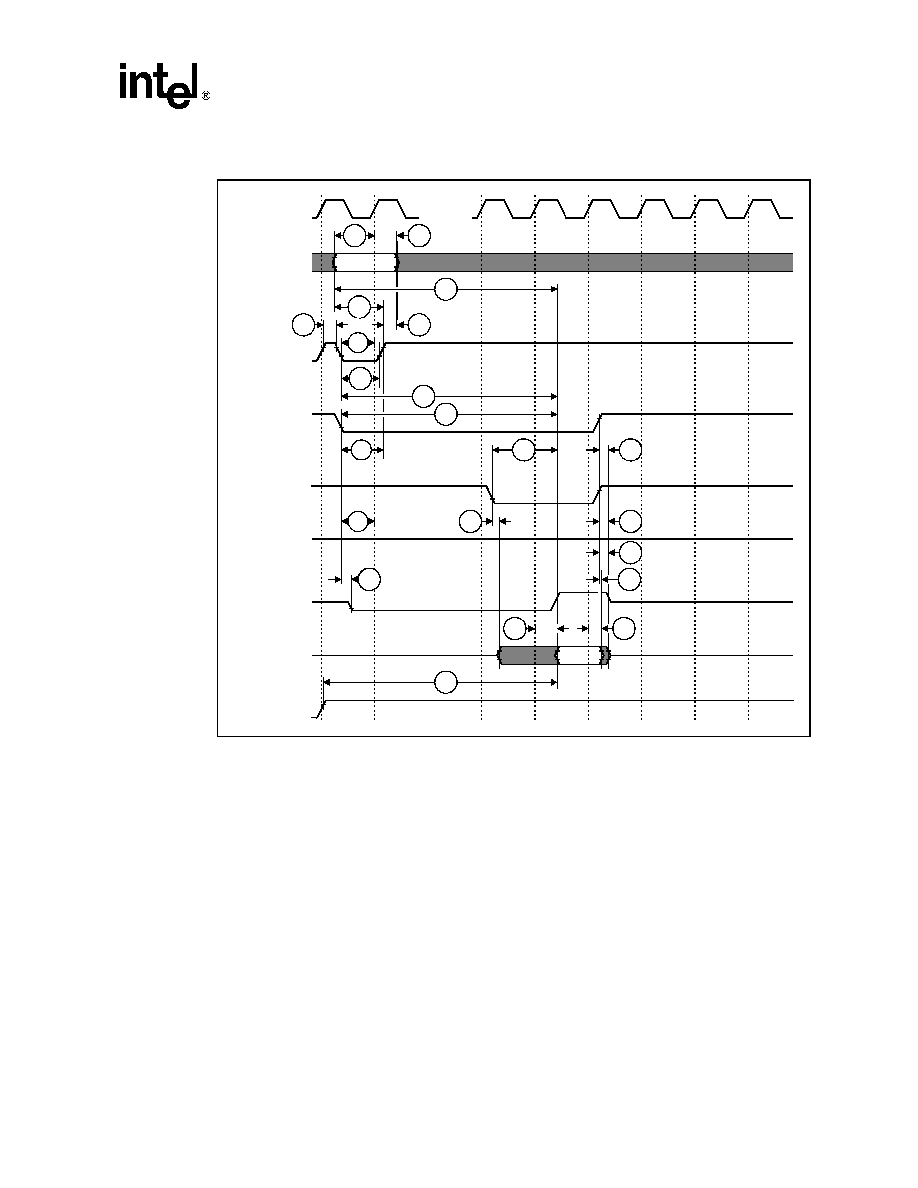
Intel
Æ
Wireless Flash Memory (W18)
Datasheet
69
NOTES:
1.
Section 8.2, "First Access Latency Count (CR[13:11])" on page 48
describes how to insert clock cycles during
the initial access.
2. WAIT (shown asserted; CR.10=0) can be configured to assert either during, or one data cycle before, valid
data.
3. This waveform illustrates the case in which an x-word burst is initiated to the main array and it is terminated
by a CE# de-assertion after the first word in the burst. If this access had been done to Status, ID, or Query
reads, the asserted (low) WAIT signal would have remained asserted (low) as long as CE# is asserted (low).
Figure 23. Single Synchronous Read-Array Operation Waveform
Note 1
V
IH
V
IL
V
IH
V
IL
V
IH
V
IL
Valid
Address
V
IH
V
IL
V
IH
V
IL
V
IH
V
IL
V
OH
V
OL
V
OH
V
OL
High Z
Valid
Output
V
IH
V
IL
R101
R102
R302
R301
R306
R2
R106
R105
R103
R3
R4
R7
R8
R9
R10
R5
R305
High Z
R304
CLK [C]
RST# [P]
Address [A]
ADV# [V]
OE# [G]
WE# [W]
WAIT [T]
Data [Q]
CE# [E]
R303
R104
High Z
R308
R309
Note 2
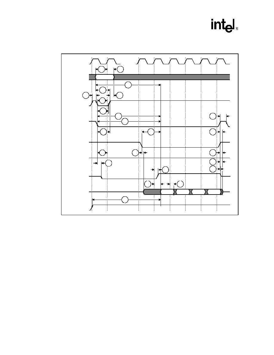
Intel
Æ
Wireless Flash Memory (W18)
70
Datasheet
NOTES:
1.
Section 8.2, "First Access Latency Count (CR[13:11])" on page 48
describes how to insert clock cycles during
the initial access.
2. WAIT (shown asserted; CR.10 = 0) can be configured to assert either during, or one data cycle before, valid
data.
Figure 24. Synchronous 4-Word Burst Read Operation Waveform
V
IH
V
IL
V
OH
V
OL
V
IH
V
IL
V
IH
V
IL
V
IH
V
IL
V
IH
V
IL
V
IH
V
IL
Valid
Address
V
IH
V
IL
Note 1
V
OH
V
OL
Valid
Output
Valid
Output
Valid
Output
Valid
Output
High Z
R105
R102
R301
R302
R306
R101
R2
R106
R103
R3
R4
R7
R304
R5
R305
R8
R9
0
1
RST# [P]
WAIT [T]
WE# [W]
OE# [G]
CE# [E]
ADV# [V]
Address [A]
CLK [C]
Data [Q]
Note 2
R104
R303
R10
R307
High Z
R308
R309
R310
High Z
High Z

Intel
Æ
Wireless Flash Memory (W18)
Datasheet
71
NOTES:
1.
Section 8.2, "First Access Latency Count (CR[13:11])" on page 48
describes how to insert clock cycles during
the initial access.
2. WAIT (shown asserted; CR.10=0) can be configured to assert either during, or one data cycle before, valid
data. (assumed wait delay of two clocks for example)
Figure 25. WAIT Functionality for EOWL (End-of-Word Line) Condition Waveform
V
IH
V
IL
V
OH
V
OL
V
IH
V
IL
V
IH
V
IL
V
IH
V
IL
V
IH
V
IL
V
IH
V
IL
Valid
Address
V
IH
V
IL
Note 1
V
OH
V
OL
Valid
Output
Valid
Output
Valid
Output
Valid
Output
High Z
R105
R102
R301
R302
R306
R101
R2
R106
R103
R3
R4
R7
R304
R5
R305
0
1
RST# [P]
WAIT [T]
WE# [W]
OE# [G]
CE# [E]
ADV# [V]
Address [A]
CLK [C]
Data [D/Q]
Note 2
R104
R303
R307
High Z
R308
High Z
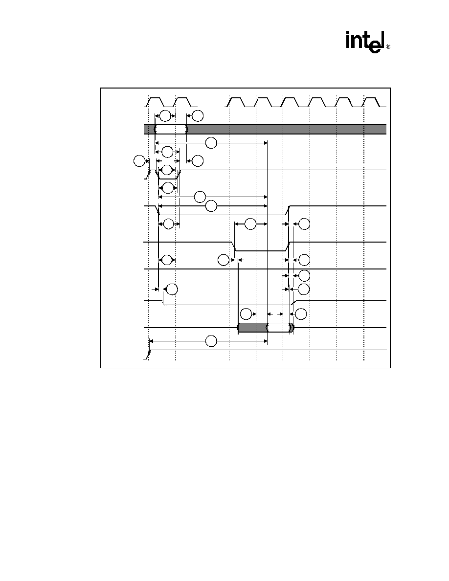
Intel
Æ
Wireless Flash Memory (W18)
72
Datasheet
NOTES:
1.
Section 8.2, "First Access Latency Count (CR[13:11])" on page 48
describes how to insert clock cycles during
the initial access.
2. WAIT shown asserted (CR.10=0).
Figure 26. WAIT Signal in Synchronous Non-Read Array Operation Waveform
Note 1
V
IH
V
IL
V
IH
V
IL
V
IH
V
IL
Valid
Address
V
IH
V
IL
V
IH
V
IL
V
IH
V
IL
V
OH
V
OL
V
OH
V
OL
High Z
Valid
Output
V
IH
V
IL
R101
R102
R302
R301
R306
R2
R106
R105
R103
R3
R4
R7
R8
R9
R10
R5
R305
High Z
R304
CLK [C]
RST# [P]
Address [A]
ADV# [V]
OE# [G]
WE# [W]
WAIT [T]
Data [Q]
CE# [E]
R303
R104
High Z
R308
R309
Note 2
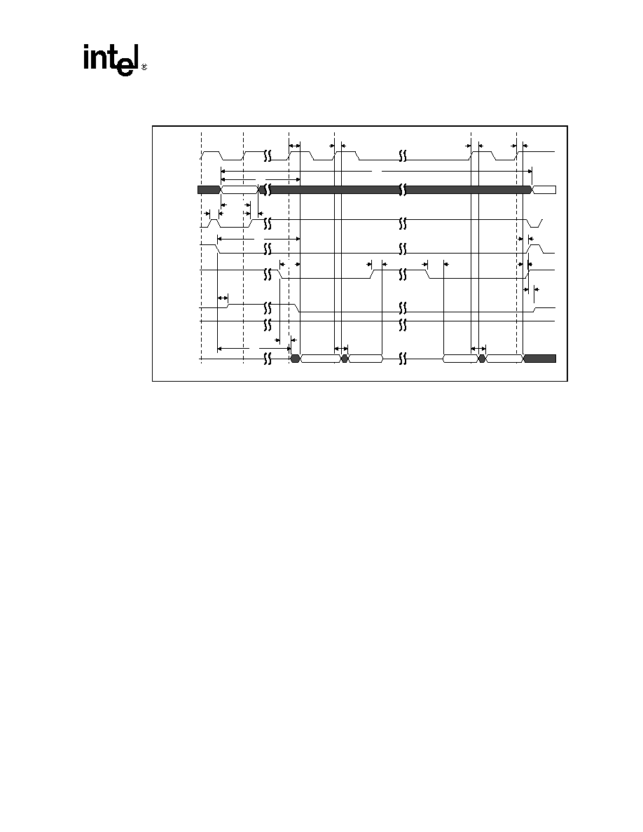
Intel
Æ
Wireless Flash Memory (W18)
Datasheet
73
NOTE:
1. During Burst Suspend Clock signal can be held high or low
Figure 27. Burst Suspend
Q0
Q1
Q1
Q2
R304
R304
R7
R6
R13
R12
R9
R4
R9
R4
R8
R3
R106
R101
R105
R105
R1
R1
R2
R305
R305
R305
R304
CLK
Address [A]
ADV#
CE# [E]
OE# [G]
WAIT [T]
WE# [W]
DATA [D/Q]

Intel
Æ
Wireless Flash Memory (W18)
74
Datasheet
11.3
AC Write Characteristics
Table 26. AC Write Characteristics
≠ .13
µ
m Lithography
#
Sym
Parameter
1,2
Notes
V
CCQ
=
1.35 V ≠ 1.8 V
V
CCQ
=
1.7 V ≠ 2.24 V
Unit
-65
-85
-60
-80
Min
Max
Min
Max
Min
Max
Min
Max
W1
t
PHWL
(t
PHEL
)
RST# High Recovery to WE#
(CE#) Low
3
150
150
150
150
ns
W2
t
ELWL
(t
WLEL
)
CE# (WE#) Setup to WE# (CE#)
Low
0
0
0
0
ns
W3
t
WLWH
(t
ELEH
)
WE# (CE#) Write Pulse Width
Low
4
50
60
40
60
ns
W4
t
DVWH
(t
DVEH
)
Data Setup to WE# (CE#) High
50
60
40
60
ns
W5
t
AVWH
(t
AVEH
)
Address Setup to WE# (CE#)
High
50
60
40
60
ns
W6
t
WHEH
(t
EHWH
)
CE# (WE#) Hold from WE# (CE#)
High
0
0
0
0
ns
W7
t
WHDX
(t
EHDX
)
Data Hold from WE# (CE#) High
0
0
0
0
ns
W8
t
WHAX
(t
EHAX
)
Address Hold from WE# (CE#)
High
0
0
0
0
ns
W9
t
WHWL
(t
EHEL
)
WE# (CE#) Pulse Width High
5,6,7
20
25
20
25
ns
W10
t
VPWH
(t
VPEH
)
VPP Setup to WE# (CE#) High
3
200
200
200
200
ns
W11
t
QVVL
VPP Hold from Valid SRD
3,8
0
0
0
0
ns
W12
t
QVBL
WP# Hold from Valid SRD
3,8
0
0
0
0
ns
W13
t
BHWH
(t
BHEH
)
WP# Setup to WE# (CE#) High
3
200
200
200
200
ns
W14
t
WHGL
(t
EHGL
)
Write Recovery before Read
0
0
0
0
ns
W16
t
WHQV
WE# High to Valid Data
3,6,10
t
AVQV
+ 25
t
AVQV
+ 55
t
AVQV
+20
t
AVQV
+50
ns
W18
t
WHAV
WE# High to Address Valid
3,9,10
0
0
0
0
ns
W19
t
WHCV
WE# High to CLK Valid
3,10
16
20
12
20
ns
W20
t
WHVH
WE# High to ADV# High
3,10
16
20
12
20
ns
NOTES:
1. Write timing characteristics during erase suspend are the same as during write-only operations.
2. A write operation can be terminated with either CE# or WE#.
3. Sampled, not 100% tested.
4. Write pulse width low (t
WLWH
or t
ELEH
) is defined from CE# or WE# low (whichever occurs last) to CE# or WE# high
(whichever occurs first). Hence, t
WLWH
= t
ELEH
= t
WLEH
= t
ELWH
.
5. Write pulse width high (t
WHWL
or t
EHEL
) is defined from CE# or WE# high (whichever is first) to CE# or WE# low (whichever is
last). Hence, t
WHWL
= t
EHEL
= t
WHEL
= t
EHWL
.
6. System designers should take this into account and may insert a software No-Op instruction to delay the first read after
issuing a command.
7. For commands other than resume commands.
8. V
PP
should be held at V
PP1
or V
PP2
until block erase or program success is determined.
9. Applicable during asynchronous reads following a write.
10.t
WHCH/L
OR t
WHVH
must be met when transitioning from a write cycle to a synchronous burst read. t
WHCH/L
and t
WHVH
both refer to
the address latching event (either the rising/falling clock edge or the rising ADV# edge, whichever occurs first).

Intel
Æ
Wireless Flash Memory (W18)
Datasheet
75
l
Table 27. AC Write Characteristics
≠ .18
µ
m Lithography
#
Sym
Parameter
1,2
Notes
32-Mbit
64-Mbit
128-Mbit
Unit
-70
-85
Min
Max
Min
Max
W1
t
PHWL
(t
PHEL
)
RST# High Recovery to WE# (CE#) Low
3
150
150
ns
W2
t
ELWL
(t
WLEL
)
CE# (WE#) Setup to WE# (CE#) Low
0
0
ns
W3
t
WLWH
(t
ELEH
)
WE# (CE#) Write Pulse Width Low
4
45
60
ns
W4
t
DVWH
(t
DVEH
)
Data Setup to WE# (CE#) High
45
60
ns
W5
t
AVWH
(t
AVEH
)
Address Setup to WE# (CE#) High
45
60
ns
W6
t
WHEH
(t
EHWH
)
CE# (WE#) Hold from WE# (CE#) High
0
0
ns
W7
t
WHDX
(t
EHDX
)
Data Hold from WE# (CE#) High
0
0
ns
W8
t
WHAX
(t
EHAX
)
Address Hold from WE# (CE#) High
0
0
ns
W9
t
WHWL
(t
EHEL
)
WE# (CE#) Pulse Width High
5,6,7
25
25
ns
W10
t
VPWH
(t
VPEH
)
VPP Setup to WE# (CE#) High
3
200
200
ns
W11
t
QVVL
VPP Hold from Valid SRD
3,8
0
0
ns
W12
t
QVBL
WP# Hold from Valid SRD
3,8
0
0
ns
W13
t
BHWH
(t
BHEH
)
WP# Setup to WE# (CE#) High
3
200
200
ns
W14
t
WHGL
(t
EHGL
)
Write Recovery before Read
0
0
ns
W16
t
WHQV
WE# High to Valid Data
3,6,10
t
AVQV
+ 40
t
AVQV
+ 50
ns
W18
t
WHAV
WE# High to Address Valid
3,9,10
0
0
ns
W19
t
WHCV
WE# High to CLK Valid
3,10
20
20
ns
W20
t
WHVH
WE# High to ADV# High
3,10
20
20
ns
NOTES:
1. Write timing characteristics during erase suspend are the same as during write-only operations.
2. A write operation can be terminated with either CE# or WE#.
3. Sampled, not 100% tested.
4. Write pulse width low (t
WLWH
or t
ELEH
) is defined from CE# or WE# low (whichever occurs last) to CE# or WE#
high (whichever occurs first). Hence, t
WLWH
= t
ELEH
= t
WLEH
= t
ELWH
.
5. Write pulse width high (t
WHWL
or t
EHEL
) is defined from CE# or WE# high (whichever is first) to CE# or WE# low
(whichever is last). Hence, t
WHWL
= t
EHEL
= t
WHEL
= t
EHWL
.
6. System designers should take this into account and may insert a software No-Op instruction to delay the first
read after issuing a command.
7. For commands other than resume commands.
8. V
PP
should be held at V
PP1
or V
PP2
until block erase or program success is determined.
9. Applicable during asynchronous reads following a write.
10.t
WHCH/L
OR t
WHVH
must be met when transitioning from a write cycle to a synchronous burst read. t
WHCH/L
and t
WHVH
both refer to the address latching event (either the rising/falling clock edge or the rising ADV# edge, whichever
occurs first).
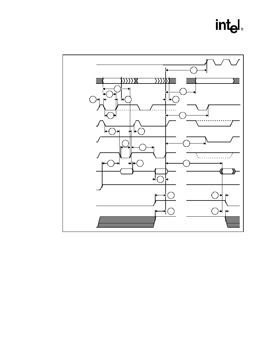
Intel
Æ
Wireless Flash Memory (W18)
76
Datasheet
NOTES:
1. V
CC
power-up and standby.
2. Write Program or Erase Setup command.
3. Write valid address and data (for program) or Erase Confirm command.
4. Automated program/erase delay.
5. Read status register data (SRD) to determine program/erase operation completion.
6. OE# and CE# must be asserted and WE# must be deasserted for read operations.
7. CLK is ignored. (but may be kept active/toggling)
Figure 28. Write Operations Waveform
Note 1
Note 2
Note 3
Note 4
Note 5
Address [A]
V
IH
V
IL
Valid
Address
Valid
Address
CE# (WE#) [E(W)]
V
IH
V
IL
Note 6
OE# [G]
V
IH
V
IL
WE# (CE#) [W(E)]
V
IH
V
IL
RST# [P]
V
IH
V
IL
W6
W7
W8
W11
W12
R105
VPP [V]
V
PPH
V
PPLK
V
IL
WP# [B]
V
IH
V
IL
Data [Q]
V
IH
V
IL
Data In
Valid
SRD
ADV# [V]
V
IH
V
IL
W16
W1
W2
W3
W4
W9
W10
W13
W14
R101
R106
Data In
Valid
Address
Note 6
R104
W5
W18
W19
W20
CLK [C]
V
IH
V
IL
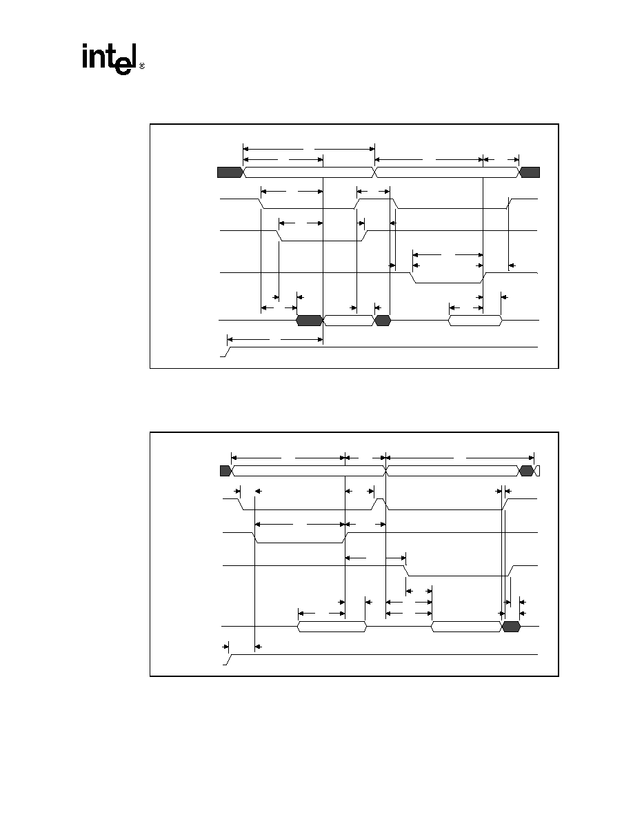
Intel
Æ
Wireless Flash Memory (W18)
Datasheet
77
Figure 29. Asynchronous Read to Write Operation Waveform
Q
D
R5
W7
W4
R10
R7
R6
W6
W3
W3
W2
R9
R4
R8
R3
W8
W5
R1
R2
R1
Address [A]
CE# [E}
OE# [G]
WE# [W]
Data [D/Q]
RST# [P]
Figure 30. Asynchronous Write to Read Operation
D
Q
W1
R9
R8
R4
R3
R2
W7
W4
W14
W18
W3
W3
R10
W6
W2
R1
R1
W8
W5
Address [A]
CE# [E}
WE# [W]
OE# [G]
Data [D/Q]
RST # [P]

Intel
Æ
Wireless Flash Memory (W18)
78
Datasheet
Figure 31. Synchronous Read to Write Operation
Latency Count
Q
D
D
W7
R13
R305
R304
R7
R307
R12
W15
W9
W19
W8
W9
W3
W3
W2
R8
R4
W6
R11
R11
R303
R3
W20
R104
R104
R106
R102
R105
R105
W18
W5
R101
R2
R306
R302
R301
CLK [C]
Addr ess [A]
ADV# [V]
CE# [E]
OE# [G]
WE#
WAIT [T]
Data [D/Q]
Figure 32. Synchronous Write To Read Operation
Lat ency Count
D
Q
Q
W1
R304
R305
R304
R3
W7
W4
R307
R12
R4
W18
W19
W3
W3
R11
R303
R11
W6
W2
W20
R104
R106
R104
R306
W8
W5
R302
R301
R2
CLK
Address [A]
ADV#
CE# [E}
WE# [W]
OE# [G ]
WAIT [T]
Data [D/Q ]
RST# [P]
Intel
Æ
Wireless Flash Memory (W18)
Datasheet
79
11.4
Erase and Program Times
Table 28. Erase and Program Times
Operation
Symbol
Parameter
Description
1
Notes
V
PP1
V
PP2
Unit
Typ
Max
Typ
Max
Erasing and Suspending
Erase Time
W500
tERS/PB
4-Kword Parameter Block
2,3
0.3
2.5
0.25
2.5
s
W501
t
ERS/MB
32-Kword Main Block
2,3
0.7
4
0.4
4
s
Suspend
Latency
W600
t
SUSP/P
Program Suspend
2
5
10
5
10
µs
W601
t
SUSP/E
Erase Suspend
2
5
20
5
20
µs
Programming
Program
Time
W200
tPROG/W
Single Word
2
12
150
8
130
µs
W201
tPROG/PB
4-Kword Parameter Block
2,3
0.05
.23
0.03
0.07
s
W202
tPROG/MB
32-Kword Main Block
2,3
0.4
1.8
0.24
0.6
s
Enhanced Factory Programming
5
Program
W400
tEFP/W
Single Word
4
N/A
N/A
3.1
16
µs
W401
tEFP/PB
4-Kword Parameter Block
2,3
N/A
15
ms
W402
tEFP/MB
32-Kword Main Block
2,3
N/A
120
ms
Operation
Latency
W403
t
EFP/SETUP
EFP Setup
N/A
5
µs
W404
t
EFP/TRAN
Program to Verify Transition
N/A
N/A
2.7
5.6
µs
W405
t
EFP/VERIFY
Verify
N/A
N/A
1.7
130
µs
NOTES:
1. Unless noted otherwise, all parameters are measured at T
A
= +25 ∞C and nominal voltages, and they are sampled, not 100%
tested.
2. Excludes external system-level overhead.
3. Exact results may vary based on system overhead.
4. W400-Typ is the calculated delay for a single programming pulse. W400-Max includes the delay when programming within a
new word-line.
5. Some EFP performance degradation may occur if block cycling exceeds 10.

Intel
Æ
Wireless Flash Memory (W18)
80
Datasheet
11.5
Reset Specifications
Table 29. Reset Specifications
#
Symbol
Parameter
1
Notes
Min
Max
Unit
P1
t
PLPH
RST# Low to Reset during Read
1, 2, 3, 4
100
ns
P2
t
PLRH
RST# Low to Reset during Block Erase
1, 3, 4, 5
20
µs
RST# Low to Reset during Program
1, 3, 4, 5
10
µs
P3
t
VCCPH
VCC Power Valid to Reset
1,3,4,5,6
60
µs
NOTES:
1. These specifications are valid for all product versions (packages and speeds).
2. The device may reset if t
PLPH
< t
PLPH
Min, but this is not guaranteed.
3. Not applicable if RST# is tied to VCC.
4. Sampled, but not 100% tested.
5. If RST# is tied to VCC, the device is not ready until t
VCCPH
occurs after when V
CC
V
CC
Min.
6. If RST# is tied to any supply/signal with V
CCQ
voltage levels, the RST# input voltage must not exceed V
CC
until V
CC
V
CC
Min.
Figure 33. Reset Operations Waveforms
(A) Reset during
read mode
(B) Reset during
program or block erase
P1
P2
(C) Reset during
program or block erase
P1
P2
V
IH
V
IL
V
IH
V
IL
V
IH
V
IL
RST# [P]
RST# [P]
RST# [P]
Abort
Complete
Abort
Complete
V
CC
0V
VCC
(D) VCC Power-up to
RST# high
P1
R5
P2
P3
P2
R5
R5
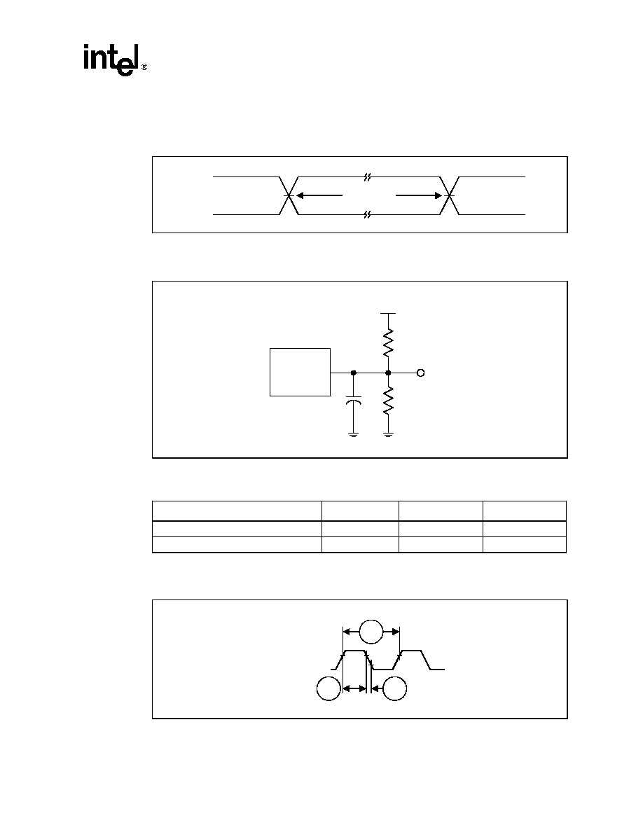
Intel
Æ
Wireless Flash Memory (W18)
Datasheet
81
11.6
AC I/O Test Conditions
NOTE:
Input timing begins, and output timing ends, at V
CCQ
/2. Input rise and fall times (10% to 90%) < 5 ns.
Worst case speed conditions are when V
CC
= V
CC
Min.
NOTE:
See Table 17 for component values.
Figure 34. AC Input/Output Reference Waveform
V
CCQ
0V
V
CCQ
/2
V
CCQ
/2
Test Points
Input
Output
Figure 35. Transient Equivalent Testing Load Circuit
Device
Under Test
V
CCQ
C
L
R
2
R
1
Out
Table 30. Test Configuration Component Values for Worst Case Speed Conditions
Test Configuration
C
L
(pF)
R
1
(k
)
R
2
(k
)
V
CCQ
Min-Extended (1.35 V) Standard Test
30
13.5
13.5
V
CCQ
Min (1.7 V) Standard Test
30
16.7
16.7
NOTE:
C
L
includes jig capacitance.
Figure 36. Clock Input AC Waveform
CLK [C]
V
IH
V
IL
R203
R202
R201

Intel
Æ
Wireless Flash Memory (W18)
82
Datasheet
11.7
Device Capacitance
T
A
= +25 ∞C, f = 1 MHz
Symbol
Parameter
ß
Typ
Max
Unit
Condition
C
IN
Input Capacitance
6
8
pF
V
IN
= 0.0 V
C
OUT
Output Capacitance
8
12
pF
V
OUT
= 0.0 V
C
CE
CE# Input Capacitance
10
12
pF
V
IN
= 0.0 V
ß
Sampled, not 100% tested.

Intel
Æ
Wireless Flash Memory (W18)
Datasheet
83
Appendix A Write State Machine States
This table shows the command state transitions based on incoming commands. Only one partition
can be actively programming or erasing at a time.
Figure 37. Write State Machine -- Next State Table (Sheet 1 of 2)
Chip Next State after Command Input
Read
Array
(3)
Program
Setup
(4,5)
Erase
Setup
(4,5)
Enhanced
Factory
Pgm
Setup
(4)
BE Confirm,
P/E Resume,
ULB
Confirm
(9)
Program/
Erase
Suspend
Read
Status
Clear
Status
Register
(6)
Read
ID/Query
(FFH)
(10H/40H)
(20H)
(30H)
(D0H)
(B0H)
(70H)
(50H)
(90H, 98H)
Ready
Ready
Program
Setup
Erase
Setup
EFP
Setup
Ready
Lock/CR Setup
Ready (Lock Error)
Ready
Ready (Lock Error)
Setup
OTP Busy
Busy
Setup
Program Busy
Busy
Program Busy
Pgm Susp
Program Busy
Suspend
Program Suspend
Pgm Busy
Program Suspend
Setup
Ready (Error)
Erase Busy
Ready (Error)
Busy
Erase Busy
Erase Susp
Erase Busy
Suspend
Erase
Suspend
Pgm in
Erase
Susp Setup
Erase Suspend
Erase Busy
Erase Suspend
Setup
Program in Erase Suspend Busy
Busy
Program in Erase Suspend Busy
Pgm Susp in
Erase Susp
Program in Erase Suspend Busy
Suspend
Program Suspend in Erase Suspend
Pgm in Erase
Susp Busy
Program Suspend in Erase Suspend
Erase Suspend (Lock Error)
Erase Susp
Erase Suspend
(Lock Error)
Setup
Ready (Error)
EFP Busy
Ready (Error)
EFP Busy
EFP Busy
(7)
EFP Verify
Verify Busy
(7)
Output Next State after Command Input
Status
Status
Status
ID/Query
Write
S
tate
Machine
(
WSM)
Next
State
T
able
Output
Next
State
T
able
(1
)
Lock/CR Setup,
Lock/CR Setup in Erase Susp
OTP Busy
Current Chip
State
(8)
Ready,
Pgm Busy,
Pgm Suspend,
Erase Busy,
Erase Suspend,
Pgm In Erase Susp Busy,
Pgm Susp In Erase Susp
Pgm Setup,
Erase Setup,
OTP Setup,
Pgm in Erase Susp Setup,
EFP Setup,
EFP Busy,
Verify Busy
Lock/CR Setup in Erase
Suspend
Erase
Program
Program in
Erase Suspend
OTP
Enhanced
Factory
Program
Output
does not
change
Array
(3)
Status
Output does not change
Status
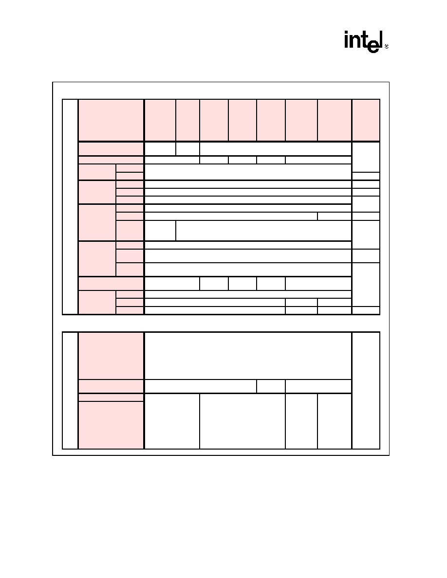
Intel
Æ
Wireless Flash Memory (W18)
84
Datasheet
NOTES:
1. The output state shows the type of data that appears at the outputs if the partition address is the same as the command
address.
A partition can be placed in Read Array, Read Status or Read ID/CFI, depending on the command issued.
Each partition stays in its last output state (Array, ID/CFI or Status) until a new command changes it. The next WSM state does
not depend on the partition's output state.
For example, if partition #1's output state is Read Array and partition #4's output state is Read Status, every read from partition
#4 (without issuing a new command) outputs the Status register.
Figure 37. Write State Machine -- Next State Table (Sheet 2 of 2)
Chip Next State after Command Input
Lock,
Unlock,
Lock-down,
CR setup
(5)
OTP
Setup
(5)
Lock
Block
Confirm
(9)
Lock-
Down
Block
Confirm
(9)
Write CR
Confirm
(9)
Enhanced
Fact Pgm
Exit (blk add
<> WA0)
Illegal
commands or
EFP data
(2)
(60H)
(C0H)
(01H)
(2FH)
(03H)
(XXXXH)
(other codes)
Ready
Lock/CR
Setup
OTP
Setup
Ready
Lock/CR Setup
Ready (Lock Error)
Ready
Ready
Ready
Ready (Lock Error)
Setup
OTP Busy
Busy
Ready
Setup
Program Busy
N/A
Busy
Program Busy
Ready
Suspend
Program Suspend
Setup
Ready (Error)
Busy
Erase Busy
Erase Busy
Ready
Suspend
Lock/CR
Setup in
Erase Susp
Erase Suspend
Setup
Program in Erase Suspend Busy
Busy
Program in Erase Suspend Busy
Erase
Suspend
Suspend
Program Suspend in Erase Suspend
Erase Suspend
(Lock Error)
Erase Susp Erase Susp Erase Susp
Erase Suspend (Lock Error)
Setup
Ready (Error)
EFP Busy
EFP Busy
(7)
EFP Verify
EFP Busy
(7)
EFP Verify
Verify Busy
(7)
Ready
EFP Verify
(7)
Ready
Output Next State after Command Input
Status
Status
Array
Status
Write
S
tate
Machine
(
WSM)
N
ext
State
T
able
Output
Next
State
T
able
(1
)
Program
Erase
Program in
Erase Suspend
Current Chip
State
(8)
OTP
Lock/CR Setup in Erase
Suspend
Enhanced
Factory
Program
Output does
not change
Output does
not change
WSM
Operation
Completes
N/A
N/A
N/A
N/A
Output does not change
Array
Status
Pgm Setup,
Erase Setup,
OTP Setup,
Pgm in Erase Susp Setup,
EFP Setup,
EFP Busy,
Verify Busy
Lock/CR Setup,
Lock/CR Setup in Erase Susp
OTP Busy
Ready,
Pgm Busy,
Pgm Suspend,
Erase Busy,
Erase Suspend,
Pgm In Erase Susp Busy,
Pgm Susp In Erase Susp

Intel
Æ
Wireless Flash Memory (W18)
Datasheet
85
2. Illegal commands are those not defined in the command set.
3. All partitions default to Read Array mode at power-up. A Read Array command issued to a busy partition results in undermined
data when a partition address is read.
4. Both cycles of 2 cycles commands should be issued to the same partition address. If they are issued to different partitions, the
second write determines the active partition. Both partitions will output status information when read.
5. If the WSM is active, both cycles of a 2 cycle command are ignored. This differs from previous Intel devices.
6. The Clear Status command clears status register error bits except when the WSM is running (Pgm Busy, Erase Busy, Pgm Busy
In Erase Suspend, OTP Busy, EFP modes) or suspended (Erase Suspend, Pgm Suspend, Pgm Suspend In Erase Suspend).
7. EFP writes are allowed only when status register bit SR.0 = 0. EFP is busy if Block Address = address at EFP Confirm
command. Any other commands are treated as data.
8. The "current state" is that of the WSM, not the partition.
9. Confirm commands (Lock Block, Unlock Block, Lock-down Block, Configuration Register) perform the operation and then move
to the Ready State.
10.In Erase suspend, the only valid two cycle commands are "Program Word", "Lock/Unlock/Lockdown Block", and "CR Write".
Both cycles of other two cycle commands ("OEM CAM program & confirm", "Program OTP & confirm", "EFP Setup & confirm",
"Erase setup & confirm") will be ignored. In Program suspend or Program suspend in Erase suspend, both cycles of all two
cycle commands will be ignored.

Appendix B Common Flash Interface
This appendix defines the data structure or "database" returned by the Common Flash Interface
(CFI) Query command. System software should parse this structure to gain critical information
such as block size, density, x8/x16, and electrical specifications. Once this information has been
obtained, the software will know which command sets to use to enable flash writes, block erases,
and otherwise control the flash component. The Query is part of an overall specification for
multiple command set and control interface descriptions called Common Flash Interface, or CFI.
B.1
Query Structure Output
The Query database allows system software to obtain information for controlling the flash device.
This section describes the device's CFI-compliant interface that allows access to Query data.
Query data are presented on the lowest-order data outputs (DQ0-7) only. The numerical offset
value is the address relative to the maximum bus width supported by the device. On this family of
devices, the Query table device starting address is a 10h, which is a word address for x16 devices.
For a word-wide (x16) device, the first two Query-structure bytes, ASCII "Q" and "R," appear on
the low byte at word addresses 10h and 11h. This CFI-compliant device outputs 00h data on upper
bytes. The device outputs ASCII "Q" in the low byte (DQ
0-7
) and 00h in the high byte (DQ
8-15
).
At Query addresses containing two or more bytes of information, the least significant data byte is
presented at the lower address, and the most significant data byte is presented at the higher address.
In all of the following tables, addresses and data are represented in hexadecimal notation, so the
"h" suffix has been dropped. In addition, since the upper byte of word-wide devices is always
"00h," the leading "00" has been dropped from the table notation and only the lower byte value is
shown. Any x16 device outputs can be assumed to have 00h on the upper byte in this mode.
Table 31. Summary of Query Structure Output as a Function of Device and Mode
Table 32. Example of Query Structure Output of x16- and x8 Devices
Device
Hex
Offset
Hex
Code
ASCII
Value
00010:
51
"Q"
Device Addresses
00011:
52
"R"
00012:
59
"Y"
Word Addressing:
Byte Addressing:
Offset
Hex Code
Value
Offset
Hex Code
Value
A
X
≠A
0
D
15
≠D
0
A
X
≠A
0
D
7
≠D
0
00010h
0051
"Q"
00010h
51
"Q"
00011h
0052
"R"
00011h
52
"R"
00012h
0059
"Y"
00012h
59
"Y"
00013h
P_ID
LO
PrVendor
00013h
P_ID
LO
PrVendor
00014h
P_ID
HI
ID #
00014h
P_ID
LO
ID #
00015h
P
LO
PrVendor
00015h
P_ID
HI
ID #
00016h
P
HI
TblAdr
00016h
...
...
00017h
A_ID
LO
AltVendor
00017h
00018h
A_ID
HI
ID #
00018h
...
...
...
...

Intel
Æ
Wireless Flash Memory (W18)
Datasheet
87
B.2
Query Structure Overview
The Query command causes the flash component to display the Common Flash Interface (CFI)
Query structure or "database." The structure sub-sections and address locations are summarized
below.
Table 33. Query Structure
NOTES:
1. Refer to the Query Structure Output section and offset 28h for the detailed definition of offset address as a
function of device bus width and mode.
2. BA = Block Address beginning location (i.e., 08000h is block 1's beginning location when the block size is
32K-word).
3. Offset 15 defines "P" which points to the Primary Intel-specific Extended Query Table.
B.3
Block Status Register
The Block Status Register indicates whether an erase operation completed successfully or whether
a given block is locked or can be accessed for flash program/erase operations.
Block Erase Status (BSR.1) allows system software to determine the success of the last block erase
operation. BSR.1 can be used just after power-up to verify that the VCC supply was not
accidentally removed during an erase operation.
Table 34. Block Status Register
NOTES:
1. BA = Block Address beginning location (i.e., 08000h is block 1's beginning location when the block size is
32K-word).
B.4
CFI Query Identification String
The Identification String provides verification that the component supports the Common Flash
Interface specification. It also indicates the specification version and supported vendor-specified
command set(s).
Offset
Sub-Section Name
Description
(1)
00000h
Manufacturer Code
00001h
Device Code
(BA+2)h
(2)
Block Status register
Block-specific information
00004-Fh Reserved
Reserved for vendor-specific information
00010h
CFI query identification string
Command set ID and vendor data offset
0001Bh
System interface information
Device timing & voltage information
00027h
Device geometry definition
Flash device layout
P
(3)
Primary Intel-specific Extended Query Table
Vendor-defined additional information specific
to the Primary Vendor Algorithm
Offset
Length
Description
Add.
Value
(BA+2)h
(1)
1
Block Lock Status Register
BA+2
--00 or --01
BA+2 (bit 0): 0 or 1
BA+2 (bit 1): 0 or 1
BSR 2≠7: Reserved for future use
BA+2
(bit 2≠7): 0
BSR.0 Block lock status
0 = Unlocked
1 = Locked
BSR.1 Block lock-down status
0 = Not locked down
1 = Locked down
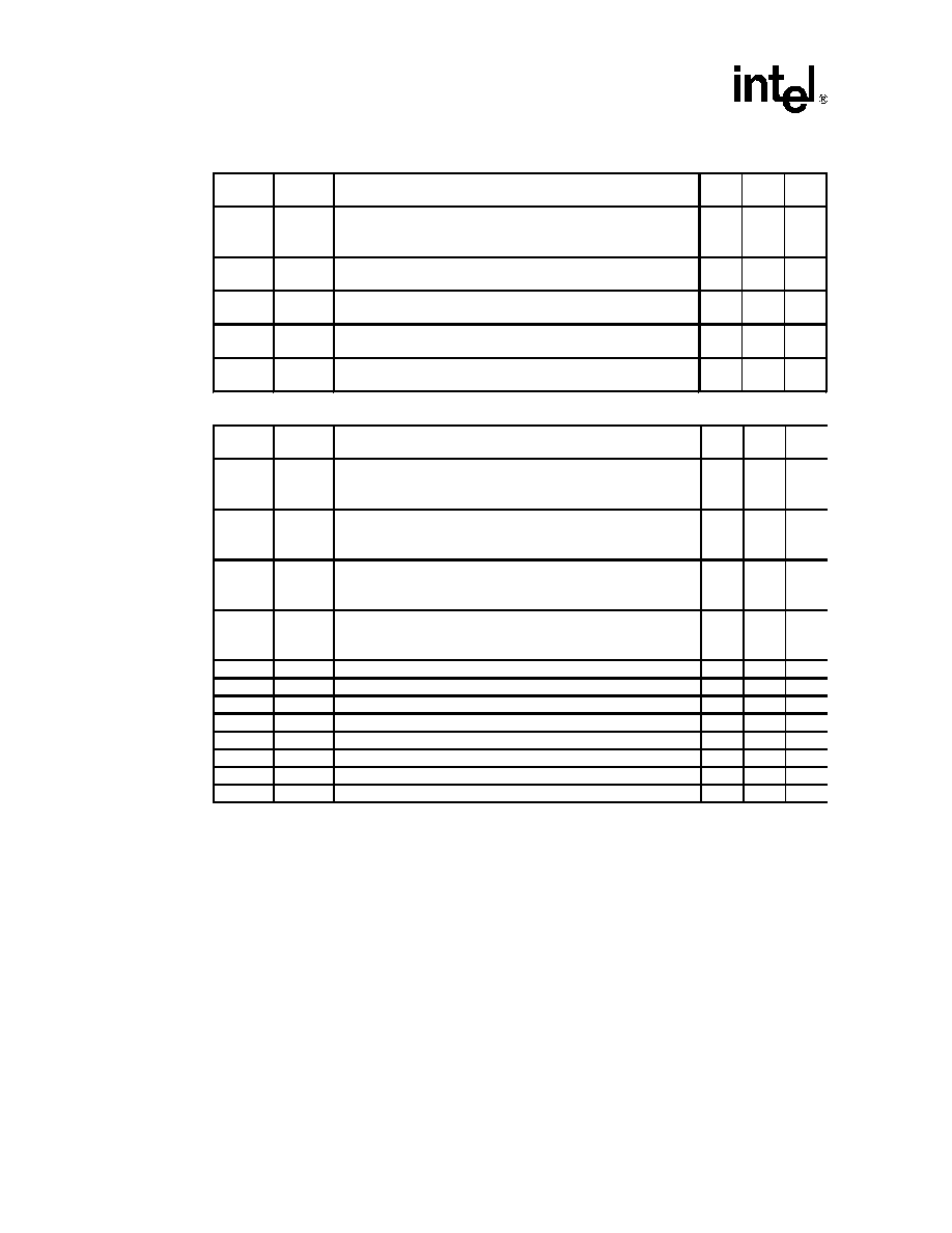
Intel
Æ
Wireless Flash Memory (W18)
88
Datasheet
Table 35. CFI Identification
Table 36. System Interface Information
Offset
Length
Description
Add.
Hex
Code Value
10h
3
Query-unique ASCII string "QRY"
10:
--51
"Q"
11:
--52
"R"
12:
--59
"Y"
13h
2
Primary vendor command set and control interface ID code.
13:
--03
16-bit ID code for vendor-specified algorithms
14:
--00
15h
2
Extended Query Table primary algorithm address
15:
--39
16:
--00
17h
2
Alternate vendor command set and control interface ID code.
17:
--00
0000h means no second vendor-specified algorithm exists
18:
--00
19h
2
Secondary algorithm Extended Query Table address.
19:
--00
0000h means none exists
1A:
--00
Offset
Length
Description
Add.
Hex
Code Value
1Bh
1
1B:
--17
1.7V
1Ch
1
1C:
--19
1.9V
1Dh
1
1D:
--B4
11.4V
1Eh
1
1E:
--C6
12.6V
1Fh
1
"n" such that typical single word program time-out = 2
n
µ-sec
1F:
--04
16µs
20h
1
"n" such that typical max. buffer write time-out = 2
n
µ-sec
20:
--00
NA
21h
1
"n" such that typical block erase time-out = 2
n
m-sec
21:
--0A
1s
22h
1
"n" such that typical full chip erase time-out = 2
n
m-sec
22:
--00
NA
23h
1
"n" such that maximum word program time-out = 2
n
times typical
23:
--04
256µs
24h
1
"n" such that maximum buffer write time-out = 2
n
times typical
24:
--00
NA
25h
1
"n" such that maximum block erase time-out = 2
n
times typical
25:
--03
8s
26h
1
"n" such that maximum chip erase time-out = 2
n
times typical
26:
--00
NA
V
CC
logic supply minimum program/erase voltage
bits 0≠3 BCD 100 mV
bits 4≠7 BCD volts
V
CC
logic supply maximum program/erase voltage
bits 0≠3 BCD 100 mV
bits 4≠7 BCD volts
V
PP
[programming] supply minimum program/erase voltage
bits 0≠3 BCD 100 mV
bits 4≠7 HEX volts
V
PP
[programming] supply maximum program/erase voltage
bits 0≠3 BCD 100 mV
bits 4≠7 HEX volts
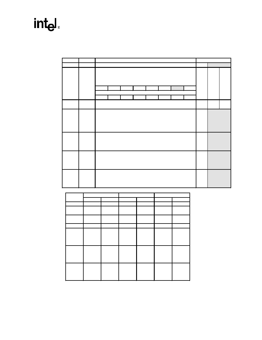
Intel
Æ
Wireless Flash Memory (W18)
Datasheet
89
B.5
Device Geometry Definition
Table 37. Device Geometry Definition
Offset
Length
Description
Code
27h
1
"n" such that device size = 2
n
in number of bytes
27:
See table below
7
6
5
4
3
2
1
0
28h
2
--
--
--
--
x64
x32
x16
x8
28:
--01
x16
15
14
13
12
11
10
9
8
--
--
--
--
--
--
--
--
29:
--00
2Ah
2
"n" such that maximum number of bytes in write buffer = 2
n
2A:
--00
0
2B:
--00
2Ch
1
2C:
2Dh
4
Erase Block Region 1 Information
2D:
bits 0≠15 = y, y+1 = number of identical-size erase blocks
2E:
bits 16≠31 = z, region erase block(s) size are z x 256 bytes
2F:
30:
31h
4
Erase Block Region 2 Information
31:
bits 0≠15 = y, y+1 = number of identical-size erase blocks
32:
bits 16≠31 = z, region erase block(s) size are z x 256 bytes
33:
34:
35h
4
Reserved for future erase block region information
35:
36:
37:
38:
See table below
See table below
See table below
See table below
Number of erase block regions (x) within device:
1. x = 0 means no erase blocking; the device erases in bulk
2. x specifies the number of device regions with one or
more contiguous same-size erase blocks.
3. Symmetrically blocked partitions have one blocking region
Flash device interface code assignment:
"n" such that n+1 specifies the bit field that represents the flash
device width capabilities as described in the table:
Address
32 Mbit
≠B
≠T
≠B
≠T
≠B
≠T
27:
--16
--16
--17
--17
--18
--18
28:
--01
--01
--01
--01
--01
--01
29:
--00
--00
--00
--00
--00
--00
2A:
--00
--00
--00
--00
--00
--00
2B:
--00
--00
--00
--00
--00
--00
2C:
--02
--02
--02
--02
--02
--02
2D:
--07
--3E
--07
--7E
--07
--FE
2E:
--00
--00
--00
--00
--00
--00
2F:
--20
--00
--20
--00
--20
--00
30:
--00
--01
--00
--01
--00
--01
31:
--3E
--07
--7E
--07
--FE
--07
32:
--00
--00
--00
--00
--00
--00
33:
--00
--20
--00
--20
--00
--20
34:
--01
--00
--01
--00
--01
--00
35:
--00
--00
--00
--00
--00
--00
36:
--00
--00
--00
--00
--00
--00
37:
--00
--00
--00
--00
--00
--00
38:
--00
--00
--00
--00
--00
--00
64 Mbit
128 Mbit

Intel
Æ
Wireless Flash Memory (W18)
90
Datasheet
B.6
Intel-Specific Extended Query Table
Table 38. Primary Vendor-Specific Extended Query
Offset
(1)
Length
Description
Hex
P = 39h
(Optional flash features and commands)
Add. Code Value
(P+0)h
3
Primary extended query table
39:
--50
"P"
(P+1)h
Unique ASCII string "PRI"
3A:
--52
"R"
(P+2)h
3B:
--49
"I"
(P+3)h
1
Major version number, ASCII
3C:
--31
"1"
(P+4)h
1
Minor version number, ASCII
3D:
--33
"3"
(P+5)h
4
Optional feature and command support (1=yes, 0=no)
3E:
--E6
(P+6)h
bits 10≠31 are reserved; undefined bits are "0." If bit 31 is
3F:
--03
(P+7)h
"1" then another 31 bit field of Optional features follows at
40:
--00
(P+8)h
the end of the bit≠30 field.
41:
--00
bit 0 Chip erase supported
bit 0 = 0
No
bit 1 Suspend erase supported
bit 1 = 1
Yes
bit 2 Suspend program supported
bit 2 = 1
Yes
bit 3 Legacy lock/unlock supported
bit 3 = 0
No
bit 4 Queued erase supported
bit 4 = 0
No
bit 5 Instant individual block locking supported
bit 5 = 1
Yes
bit 6 Protection bits supported
bit 6 = 1
Yes
bit 7 Pagemode read supported
bit 7 = 1
Yes
bit 8 Synchronous read supported
bit 8 = 1
Yes
bit 9 Simultaneous operations supported
bit 9 = 1
Yes
(P+9)h
1
42:
--01
bit 0 Program supported after erase suspend
bit 0 = 1
Yes
(P+A)h
2
Block status register mask
43:
--03
(P+B)h
bits 2≠15 are Reserved; undefined bits are "0"
44:
--00
bit 0 Block Lock-Bit Status register active
bit 0 = 1
Yes
bit 1 Block Lock-Down Bit Status active
bit 1 = 1
Yes
(P+C)h
1
45:
--18
1.8V
(P+D)h
1
46:
--C0
12.0V
Supported functions after suspend: read Array, Status, Query
Other supported operations are:
bits 1≠7 reserved; undefined bits are "0"
V
CC
logic supply highest performance program/erase voltage
bits 0≠3 BCD value in 100 mV
bits 4≠7 BCD value in volts
V
PP
optimum program/erase supply voltage
bits 0≠3 BCD value in 100 mV
bits 4≠7 HEX value in volts

Intel
Æ
Wireless Flash Memory (W18)
Datasheet
91
Table 39. Protection Register Information
Table 40. Burst Read Information for Non-muxed Device
Table 41. Partition and Erase-block Region Information
Offset
(1)
Length
Description
Hex
P = 39h
(Optional flash features and commands)
Add.
Code Value
(P+E)h
1
47:
--01
1
(P+F)h
4
Protection Field 1: Protection Description
48:
--80
80h
(P+10)h
This field describes user-available One Time Programmable
49:
--00
00h
(P+11)h
(OTP) Protection register bytes. Some are pre-programmed
4A:
--03
8 byte
(P+12)h
4B:
--03
8 byte
Number of Protection register fields in JEDEC ID space.
"00h," indicates that 256 protection fields are available
with device-unique serial numbers. Others are user
programmable. Bits 0≠15 point to the Protection register Lock
byte, the section's first byte. The following bytes are factory
pre-programmed and user-programmable.
bits 0≠7 = Lock/bytes Jedec-plane physical low address
bits 8≠15 = Lock/bytes Jedec-plane physical high address
bits 16≠23 = "n" such that 2n = factory pre-programmed bytes
bits 24≠31 = "n" such that 2n = user programmable bytes
Offset
(1)
Length
Description
Hex
P = 39h
(Optional flash features and commands)
Add.
Code Value
(P+13)h
1
4C:
--03
8 byte
(P+14)h
1
4D:
--04
4
(P+15)h
1
4E:
--01
4
(P+16)h
1
Synchronous mode read capability configuration 2
4F:
--02
8
(P+17)h
1
Synchronous mode read capability configuration 3
50:
--03
16
(P+18)h
1
Synchronous mode read capability configuration 4
51:
--07
Cont
Page Mode Read capability
bits 0≠7 = "n" such that 2
n
HEX value represents the number of
read-page bytes. See offset 28h for device word width to
determine page-mode data output width. 00h indicates no
read page buffer.
Number of synchronous mode read configuration fields that
follow. 00h indicates no burst capability.
Synchronous mode read capability configuration 1
Bits 3≠7 = Reserved
bits 0≠2 "n" such that 2
n+1
HEX value represents the
maximum number of continuous synchronous reads when
the device is configured for its maximum word width. A value
of 07h indicates that the device is capable of continuous
linear bursts that will output data until the internal burst
counter reaches the end of the device's burstable address
space. This field's 3-bit value can be written directly to the
Read Configuration Register bits 0≠2 if the device is
configured for its maximum word width. See offset 28h for
word width to determine the burst data output width.
Offset
(1)
See table below
P = 39h
Description
Address
Bottom
Top
(Optional flash features and commands)
Len
Bot
Top
(P+19)h
(P+19)h
1
52:
52:
Number of device hardware-partition regions within the device.
x = 0: a single hardware partition device (no fields follow).
x specifies the number of device partition regions containing
one or more contiguous erase block regions.

Intel
Æ
Wireless Flash Memory (W18)
92
Datasheet
Partition Region 1 Information
Offset
(1)
See table below
P = 39h
Description
Address
Bottom
Top
(Optional flash features and commands)
Len
Bot
Top
(P+1A)h
(P+1A)h Number of identical partitions within the partition region
2
53:
53:
(P+1B)h
(P+1B)h
54:
54:
(P+1C)h
(P+1C)h
1
55:
55:
(P+1D)h
(P+1D)h
1
56:
56:
(P+1E)h
(P+1E)h
1
57:
57:
(P+1F)h
(P+1F)h
1
58:
58:
(P+20)h
(P+20)h Partition Region 1 Erase Block Type 1 Information
4
59:
59:
(P+21)h
(P+21)h
bits 0≠15 = y, y+1 = number of identical-size erase blocks
5A:
5A:
(P+22)h
(P+22)h
bits 16≠31 = z, region erase block(s) size are z x 256 bytes
5B:
5B:
(P+23)h
(P+23)h
5C:
5C:
(P+24)h
(P+24)h Partition 1 (Erase Block Type 1)
2
5D:
5D:
(P+25)h
(P+25)h
Minimum block erase cycles x 1000
5E:
5E:
(P+26)h
(P+26)h
1
5F:
5F:
(P+27)h
(P+27)h
1
60:
60:
(P+28)h
Partition Region 1 Erase Block Type 2 Information
4
61:
(P+29)h
bits 0≠15 = y, y+1 = number of identical-size erase blocks
62:
(P+2A)h
bits 16≠31 = z, region erase block(s) size are z x 256 bytes
63:
(P+2B)h
(bottom parameter device only)
64:
(P+2C)h
Partition 1 (Erase block Type 2)
2
65:
(P+2D)h
Minimum block erase cycles x 1000
66:
(P+2E)h
1
67:
(P+2F)h
1
68:
Simultaneous program or erase operations allowed in other
partitions while a partition in this region is in Program mode
bits 0≠3 = number of simultaneous Program operations
bits 4≠7 = number of simultaneous Erase operations
Simultaneous program or erase operations allowed in other
partitions while a partition in this region is in Erase mode
bits 0≠3 = number of simultaneous Program operations
bits 4≠7 = number of simultaneous Erase operations
Number of program or erase operations allowed in a partition
bits 0≠3 = number of simultaneous Program operations
bits 4≠7 = number of simultaneous Erase operations
Partition 1 (erase block Type 1) bits per cell; internal ECC
bits 0≠3 = bits per cell in erase region
bit 4 = reserved for "internal ECC used" (1=yes, 0=no)
bits 5≠7 = reserve for future use
Partition 1 (erase block Type 1) page mode and synchronous
mode capabilities defined in Table 10.
bit 0 = page-mode host reads permitted (1=yes, 0=no)
bit 1 = synchronous host reads permitted (1=yes, 0=no)
bit 2 = synchronous host writes permitted (1=yes, 0=no)
bits 3≠7 = reserved for future use
Partition 1 (Erase block Type 2) bits per cell
bits 0≠3 = bits per cell in erase region
bit 4 = reserved for "internal ECC used" (1=yes, 0=no)
bits 5≠7 = reserve for future use
Partition 1 (Erase block Type 2) pagemode and synchronous
mode capabilities defined in Table 10
bit 0 = page-mode host reads permitted (1=yes, 0=no)
bit 1 = synchronous host reads permitted (1=yes, 0=no)
bit 2 = synchronous host writes permitted (1=yes, 0=no)
bits 3≠7 = reserved for future use
Types of erase block regions in this Partition Region.
x = 0 = no erase blocking; the Partition Region erases in bulk
x = number of erase block regions w/ contiguous same-size
erase blocks. Symmetrically blocked partitions have one
blocking region. Partition size = (Type 1 blocks)x(Type 1
block sizes) + (Type 2 blocks)x(Type 2 block sizes) +...+
(Type n blocks)x(Type n block sizes)

Intel
Æ
Wireless Flash Memory (W18)
Datasheet
93
Partition Region 2 Information
Offset
(1)
See table below
P = 39h
Description
Address
Bottom
Top
(Optional flash features and commands)
Len
Bot
Top
(P+30)h
(P+28)h Number of identical partitions within the partition region
2
69:
61:
(P+31)h
(P+29)h
6A:
62:
(P+32)h
(P+2A)h
1
6B:
63:
(P+33)h
(P+2B)h
1
6C:
64:
(P+34)h
(P+2C)h
1
6D:
65:
(P+35)h
(P+2D)h
1
6E:
66:
(P+36)h
(P+2E)h Partition Region 2 Erase Block Type 1 Information
4
6F:
67:
(P+37)h
(P+2F)h
bits 0≠15 = y, y+1 = number of identical-size erase blocks
70:
68:
(P+38)h
(P+30)h
bits 16≠31 = z, region erase block(s) size are z x 256 bytes
71:
69:
(P+39)h
(P+31)h
72:
6A:
(P+3A)h
(P+32)h Partition 2 (Erase block Type 1)
2
73:
6B:
(P+3B)h
(P+33)h
Minimum block erase cycles x 1000
74:
6C:
(P+3C)h
(P+34)h
1
75:
6D:
(P+3D)h
(P+35)h
1
76:
6E:
(P+36)h Partition Region 2 Erase Block Type 2 Information
4
6F:
(P+37)h
bits 0≠15 = y, y+1 = number of identical-size erase blocks
70:
(P+38)h
bits 16≠31 = z, region erase block(s) size are z x 256 bytes
71:
(P+39)h
72:
(P+3A)h Partition 2 (Erase Block Type 2)
2
73:
(P+3B)h
Minimum block erase cycles x 1000
74:
(P+3C)h
1
75:
(P+3D)h
1
76:
(P+3E)h
(P+3E)h Features Space definitions (Reserved for future use)
TBD
77:
77:
(P+3F)h
(P+3F)h Reserved for future use
Resv'd
78:
78:
Partition 2 (Erase Block Type 2) bits per cell
bits 0≠3 = bits per cell in erase region
bit 4 = reserved for "internal ECC used" (1=yes, 0=no)
bits 5≠7 = reserved for future use
Partition 2 (Erase block Type 2) pagemode and synchronous
mode capabilities as defined in Table 10.
bit 0 = page-mode host reads permitted (1=yes, 0=no)
bit 1 = synchronous host reads permitted (1=yes, 0=no)
bit 2 = synchronous host writes permitted (1=yes, 0=no)
bits 3≠7 = reserved for future use
Simultaneous program or erase operations allowed in other
partitions while a partition in this region is in Erase mode
bits 0≠3 = number of simultaneous Program operations
bits 4≠7 = number of simultaneous Erase operations
Types of erase block regions in this Partition Region.
x = 0 = no erase blocking; the Partition Region erases in bulk
x = number of erase block regions w/ contiguous same-size
erase blocks. Symmetrically blocked partitions have one
blocking region. Partition size = (Type 1 blocks)x(Type 1
block sizes) + (Type 2 blocks)x(Type 2 block sizes) +...+
(Type n blocks)x(Type n block sizes)
Partition 2 (Erase block Type 1) bits per cell
bits 0≠3 = bits per cell in erase region
bit 4 = reserved for "internal ECC used" (1=yes, 0=no)
bits 5≠7 = reserve for future use
Partition 2 (erase block Type 1) pagemode and synchronous
mode capabilities as defined in Table 10.
bit 0 = page-mode host reads permitted (1=yes, 0=no)
bit 1 = synchronous host reads permitted (1=yes, 0=no)
bit 2 = synchronous host writes permitted (1=yes, 0=no)
bits 3≠7 = reserved for future use
Simultaneous program or erase operations allowed in other
partitions while a partition in this region is in Program mode
bits 0≠3 = number of simultaneous Program operations
bits 4≠7 = number of simultaneous Erase operations
Number of program or erase operations allowed in a partition
bits 0≠3 = number of simultaneous Program operations
bits 4≠7 = number of simultaneous Erase operations
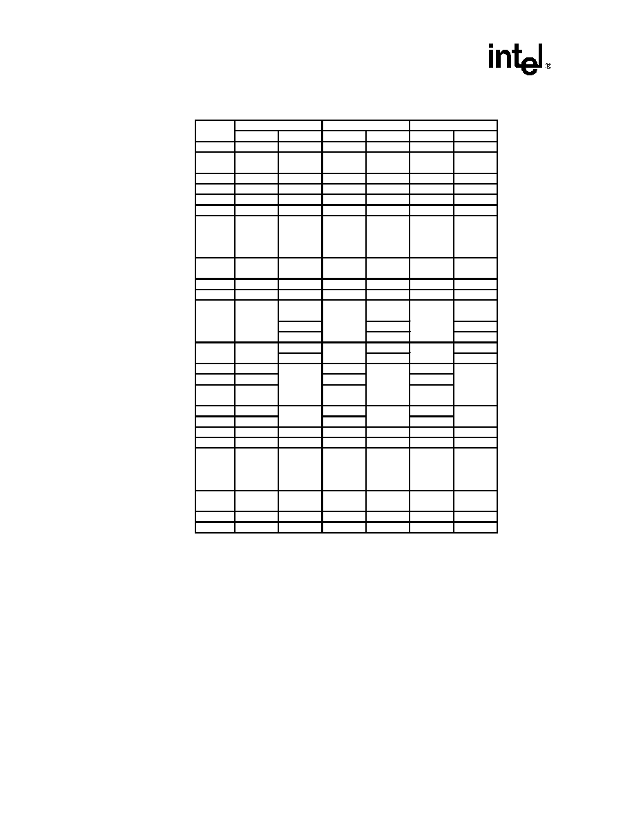
Intel
Æ
Wireless Flash Memory (W18)
94
Datasheet
Partition and Erase-block Region Information
NOTES:
1. The variable P is a pointer which is defined at CFI offset 15h.
2. TPD - Top parameter device; BPD - Bottom parameter device.
3. Partition: Each partition is 4Mb in size. It can contain main blocks OR a combination of both main and
parameter blocks.
4. Partition Region: Symmetrical partitions form a partition region. (there are two partition regions, A. contains
all the partitions that are made up of main blocks only. B. contains the partition that is made up of the
parameter and the main blocks.
Address
32 Mbit
≠B
≠T
≠B
≠T
≠B
≠T
52:
--02
--02
--02
--02
--02
--02
53:
--01
--07
--01
--0F
--01
--1F
54:
--00
--00
--00
--00
--00
--00
55:
--11
--11
--11
--11
--11
--11
56:
--00
--00
--00
--00
--00
--00
57:
--00
--00
--00
--00
--00
--00
58:
--02
--01
--02
--01
--02
--01
59:
--07
--07
--07
--07
--07
--07
5A:
--00
--00
--00
--00
--00
--00
5B:
--20
--00
--20
--00
--20
--00
5C:
--00
--01
--00
--01
--00
--01
5D:
--64
--64
--64
--64
--64
--64
5E:
--00
--00
--00
--00
--00
--00
5F:
--01
--01
--01
--01
--01
--01
60:
--03
--03
--03
--03
--03
--03
61:
--06
--01
--06
--01
--06
--01
62:
--00
--00
--00
--00
--00
--00
63:
--00
--11
--00
--11
--00
--11
64:
--01
--00
--01
--00
--01
--00
65:
--64
--00
--64
--00
--64
--00
66:
--00
--02
--00
--02
--00
--02
67:
--01
--06
--01
--06
--01
--06
68:
--03
--00
--03
--00
--03
--00
69:
--07
--00
--0F
--00
--1F
--00
6A:
--00
--01
--00
--01
--00
--01
6B:
--11
--64
--11
--64
--11
--64
6C:
--00
--00
--00
--00
--00
--00
6D:
--00
--01
--00
--01
--00
--01
6E:
--01
--03
--01
--03
--01
--03
6F:
--07
--07
--07
--07
--07
--07
70:
--00
--00
--00
--00
--00
--00
71:
--00
--20
--00
--20
--00
--20
72:
--01
--00
--01
--00
--01
--00
73:
--64
--64
--64
--64
--64
--64
74:
--00
--00
--00
--00
--00
--00
75:
--01
--01
--01
--01
--01
--01
76:
--03
--03
--03
--03
--03
--03
64Mbit
128Mbit
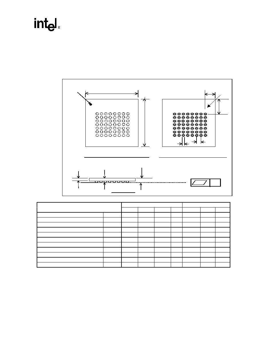
Intel
Æ
Wireless Flash Memory (W18)
Datasheet
95
Appendix C Mechanical Specifications
C.1
W18 ≠ .18
µ
m Lithography
Figure 38.
64-Mb
µ
BGA*CSP Package Drawing and Dimensions
A
2
B o tto m V ie w - B u m p s id e U p
T o p V ie w - S ilico n b a ck s id e
C o m p le te In k M a rk N o t
S id e
A
A
1
S e a ti
P la n
Y
s
2
P in # 1
In d ic a to r
E
b
P in # 1
C o rn e r
s
1
e
D
1
2
3
4
5
6
7
8
A
B
C
D
E
F
G
8
7
6
5
4
3
2
1
A
B
C
D
E
F
G
Millimeters
Inches
Symbol
Min
Nom
Max
Notes
Min
Nom
Max
Package Height
A
0.850
1.000
0.0335
0.0394
Ball Height
A1
0.150
0.0059
Package Body Thickness
A2
0.612
0.712
0.812
0.0241
0.0280
0.0320
Ball (Lead) Width
b
0.300
0.350
0.400
0.0118
0.0138
0.0157
Package Body Width
D
7.600
7.700
7.800
0.2992
0.3031
0.3071
Package Body Length
E
8.900
9.000
9.100
0.3503
0.3543
0.3583
Pitch
[e]
0.750
0.0295
Ball (Lead) Count
N
56
56
Seating Plane Coplanarity
Y
0.100
0.0039
Corner to Ball A1 Distance Along D
S1
1.125
1.225
1.325
0.0443
0.0482
0.0522
Corner to Ball A1 Distance Along E
S2
2.150
2.250
2.350
0.0846
0.0886
0.0925
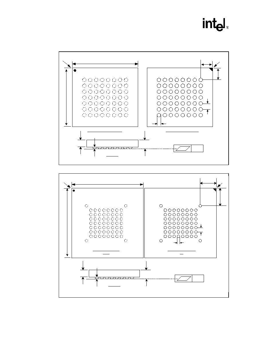
Intel
Æ
Wireless Flash Memory (W18)
96
Datasheet
Figure 39. 32-Mb VFBGA Package Drawing
Figure 40. 128-Mb VFBGA Package Drawing
E
S eating
P lane
To p View - Bump Side Down
Bottom View - Ball Side Up
Y
A
A1
D
A2
2
Ball A1
Corner
S
1
S
e
b
Ball A1
Corner
A
B
C
D
E
F
G
8
7
6
5
4
3
2
1
8
7
6
5
4
3
2
1
A
B
C
D
E
F
G
Note: Drawing not to scale
Side V iew
Seating
Plane
Y
A
A1
A2
Note: Drawing not to scal e
Side View
E
Top View - Bump Side
Down
Bottom View - Ball Side
Up
D
Ball A1
Corner
S1
S2
e
b
7
6
5
4
3
2 1
10
9
8
A
B
C
D
E
F
G
H
J
7
6
5
4
3
2
1
10
9
8
A
B
C
D
E
F
G
H
J
Ball A1
Corner

Intel
Æ
Wireless Flash Memory (W18)
Datasheet
97
Table 42. 32-Mbit and 128-Mbit VFBGA Package Dimensions
Dimension
Symbol
Millimeters
Inches
Min
Nom
Max
Min
Nom
Max
Package Height
A
0.850
1.000
0.0335
0.0394
Ball Height
A
1
0.150
0.0059
Package Body Thickness
A
2
0.615
0.665
0.715
0.0242
0.0262
0.0281
Ball (Lead) Width
b
0.325
0.375
0.425
0.0128
0.0148
0.0167
Package Body Width 32Mb
D
7.600
7.700
7.800
0.2992
0.3031
0.3071
Package Body Length32Mb
E
8.900
9.000
9.100
0.3503
0.3543
0.3583
Package Body Width 128Mb
D
12.400
12.500
12.600
0.4882
0.4921
0.4961
Package Body Length 128Mb
E
11.900
12.000
12.100
0.4685
0.4724
0.4764
Pitch
[e]
0.750
0.0295
Ball (Lead) Count 32Mb
N
56
56
Ball (Lead) Count 128Mb
N
60
60
Seating Plane Coplanarity
Y
0.100
0.0039
Corner to Ball A1 Distance Along D
32Mb
S
1
1.125
1.225
1.325
0.0443
0.0482
0.0522
Corner to Ball A1 Distance Along E
32Mb
S
2
2.150
2.250
2.350
0.0846
0.0886
0.0925
Corner to Ball A1 Distance Along D
128Mb
S
1
2.775
2.875
2.975
0.1093
0.1132
0.1171
Corner to Ball A1 Distance Along E
128Mb
S
2
2.900
3.000
3.1000
0.1142
0.1181
0.1220
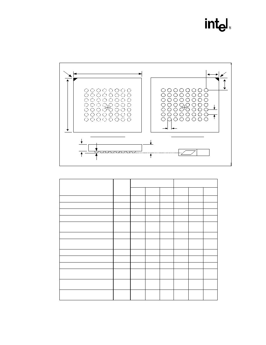
Intel
Æ
Wireless Flash Memory (W18)
98
Datasheet
C.2
W18 ≠ .13
µ
m Lithography
Figure 41.
32-, 64- and 128-Mb VF BGA*CSP Package Drawing
Table 43. 32-Mbit, 64-Mbit, and 128-Mbit VFBGA Package Dimensions
Dimension
Symbol
Millimeters
Inches
Min
Nom
Max
Min
Nom
Max
Package Height
A
1.000
0.0394
Ball Height
A
1
0.150
0.0059
Package Body Thickness
A
2
0.665
0.0262
Ball (Lead) Width
b
0.325
0.375
0.425
0.0128
0.0148
0.0167
Package Body Width (32Mb,
64Mb)
D
7.600
7.700
7.800
0.2992
0.3031
0.3071
Package Body Width (128Mb)
D
10.900
11.000
11.100
0.4291
0.4331
0.4370
Package Body Length (32Mb,
64Mb, 128Mb)
E
8.900
9.000
9.100
0.3504
0.3543
0.3583
Pitch
[e]
0.750
0.0295
Ball (Lead) Count
N
56
56
Seating Plane Coplanarity
Y
0.100
0.0039
Corner to Ball A1 Distance
Along D (32Mb, 64Mb)
S
1
1.125
1.225
1.325
0.0443
0.0482
0.0522
Corner to Ball A1 Distance
Along D (128Mb)
S
1
2.775
2.2875
2.975
0.1093
0.1132
0.1171
Corner to Ball A1 Distance
Along E (32Mb, 64Mb,128Mb)
S
2
2.150
2.250
2.350
0.0846
0.0886
0.0925
E
S eating
P lane
Top V iew - Bump S ide Dow n
Bottom Vie w - Ba ll Sid e Up
Y
A
A 1
D
A 2
2
B all A 1
Corner
8
7
6
5
4
3
2
1
A
B
C
D
E
F
G
S
1
S
e
b
B all A 1
Corner
8
7
6
5
4
3
2
1
A
B
C
D
E
F
G
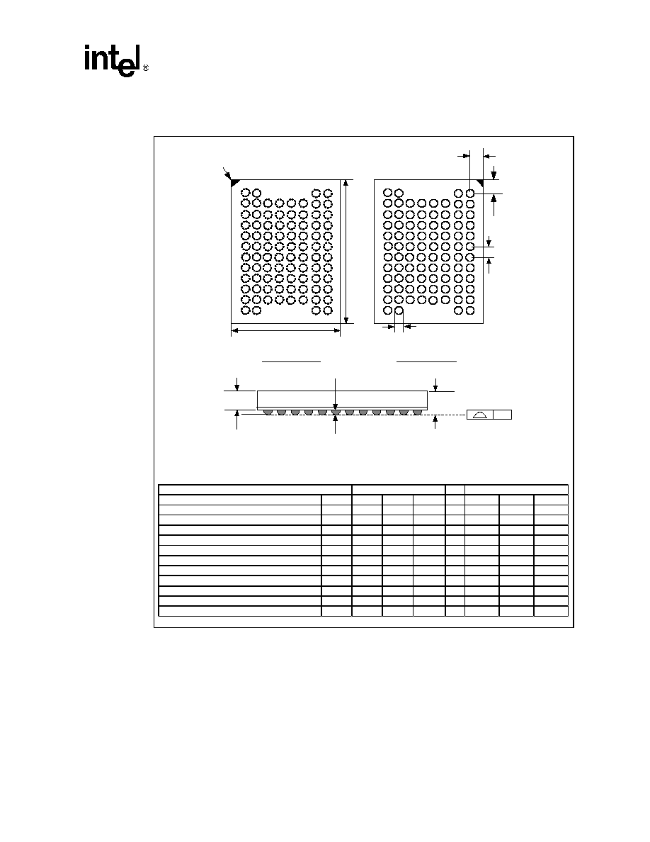
Intel
Æ
Wireless Flash Memory (W18)
Datasheet
99
Figure 42. 128Mbit QUAD+ Package Drawing
Millimeters
Inches
Dimensions
Symbol
Min
Nom
Max
Notes
Min
Nom
Max
Package Height
A
1.200
0.0472
Ball Height
A1
0.200
0.0079
Package Body Thickness
A2
0.860
0.0339
Ball (Lead) Width
b
0.325
0.375
0.425
0.0128
0.0148
0.0167
Package Body Length
D
9.900
10.000
10.100
0.3898
0.3937
0.3976
Package Body Width
E
7.900
8.000
8.100
0.3110
0.3150
0.3189
Pitch
e
0.800
0.0315
Ball (Lead) Count
N
88
88
Seating Plane Coplanarity
Y
0.100
0.0039
Corner to Ball A1 Distance Along E
S1
1.100
1.200
1.300
0.0433
0.0472
0.0512
Corner to Ball A1 Distance Along D
S2
0.500
0.600
0.700
0.0197
0.0236
0.0276
Top View - Ball Down
Bottom View - Ball Up
A
A2
D
E
Y
A1
Drawing not to scale.
S2
S1
A
C
B
E
D
G
F
J
H
K
L
M
e
1
2
3
4
5
6
7
8
b
A
C
B
E
D
G
F
J
H
K
L
M
A1 Index
Mark
1
2
3
4
5
6
7
8
Intel
Æ
Wireless Flash Memory (W18)
100
Datasheet
Appendix D Ordering Information
Figure 43. VF BGA and µBGA Ordering Information
Figure 44. SCSP Ordering Information
Package:
GE = 0.75 mm VF BGA
GT = 0.75 mm µ BGA*
Product Line Designator:
for all Intel Flash Products
Device Density:
320 = 32Mbit
640 = 64Mbit
128 = 128Mbit
Product Family:
W18 = Intel
Æ
Wireless Flash
Memory
Parameter Location:
T = Top Parameter
B = Bottom Parameter
Process Identifier:
C = 0.18
µ
m
D = 0.13
µ
m
Access Speed (ns)
(60,80)
G E 2 8 F 6 4 0 W 1 8 T D 6 0
Package:
RD = SCSP, Leaded
PF = SCSP, Pb-Free
Product Line:
48F = Flash Only
Flash Density:
0 = No die
3 = 128 Mbit
Product Family Designator:
W = Intel
Æ
Wireless Flash Memory
Voltage:
Y
= 1.8 Volt I/O
Ballout Indicator:
Q= QUAD+
Parameter Location:
T = Top Parameter
B = Bottom Parameter
Device Details:
0 = Initial Version
Fl
a
s
h
1
&
2
Fl
a
s
h
3
&
4
Fl
a
s
h
1
Fl
a
s
h
2
Fl
a
s
h
3
Fl
a
s
h
4
R D 4 8 F 3 0 0 0 W 0 Y B Q 0