Document Outline
- TITLE PAGE
- CONTENTS
- REVISION HISTORY
- 1.0 INTRODUCTION
- 1.1 Smart 3 Advanced Boot Block Flash Memory Enhancements
- 1.2 Product Overview
- 2.0 PRODUCT DESCRIPTION
- 2.1 Package Pinouts
- 2.2 Block Organization
- 2.2.1 Parameter Blocks
- 2.2.2 Main Blocks
- 3.0 PRINCIPLES OF OPERATION
- 3.1 Bus Operation
- 3.1.1 Read
- 3.1.2 Output Disable
- 3.1.3 Standby
- 3.1.4 Deep Power-Down/Reset
- 3.1.5 Write
- 3.2 Modes of Operation
- 3.2.1 Read Array
- 3.2.2 Read Intelligent Identifier
- 3.2.3 Read Status Register
- 3.2.3.1 Clearing the Status Register
- 3.2.4 Program Mode
- 3.2.4.1 Suspending and Resuming Program
- 3.2.4.2 VPP Supply Voltage during Program
- 3.2.5 Erase Mode
- 3.2.5.1 Suspending and Resuming Erase
- 3.2.5.2 VPP Supply Voltage during Erase
- 3.3 Block Locking
- 3.3.1 VPP = VIL for Complete Protection
- 3.3.2 WP# = VIL for Block Locking
- 3.3.3 WP# = VIH for Block Unlocking
- 3.4 VPP Program and Erase Voltages
- 3.5 Power Consumption
- 3.5.1 Active Power
- 3.5.2 Automatic Power Savings
- 3.5.3 Standby Power
- 3.5.4 Deep Power-Down Mode
- 3.6 Power-Up/Down Operation
- 3.6.1 RP# Connected to System Reset
- 3.6.2 VCC, VPP and RP# Transitions
- 3.7 Power Supply Decoupling
- 3.7.1 VPP Trace on Printed circuit Boards
- 4.0 ABSOLUTE MAXIMUM RATINGS
- 5.0 OPERATING CONDITIONS (VCCQ = 2.7VÖ3.6V)
- 5.1 DC Characteristics: VCCQ = 2.7VÖ3.6V
- 6.0 OPERATING CONDITIONS (VCCQ = 1.8VÖ2.2V)
- 6.1 DC Characteristics: VCCQ = 1.8VÖ2.2V
- 7.0 AC CHARACTERISTICS
- APPENDIX A: Ordering Information
- APPENDIX B: Write State Machine Current/Next States
- APPENDIX C: Access Time vs. Capacitive Load
- APPENDIX D: Architecture Block Diagram
- APPENDIX E: Additional Information
- FIGURES
- Figure 1. 48-Lead TSOP Package
- Figure 2. 4-Mbit 48-Ball µBGA* Chip Size Package
- Figure 3. 8-Mbit 48-Ball µBGA* Chip Size Package
- Figure 4. 16-Mbit 48-Ball µBGA* Chip Size Package
- Figure 5. 4-/8-/16-Mbit Advanced Boot Block Word-Wide Top Boot Memory Maps
- Figure 6. 4-/8-/16-Mbit Advanced Boot Block Word-Wide Top Boot Memory Maps
- Figure 7. Automated Word Programming Flowchart
- Figure 8. Program Suspend/Resume Flowchart
- Figure 9. Automated Block Erase Flowchart
- Figure 10. Erase Suspend/Resume Flowchart
- Figure 11. 2.7VÖ3.6V Input Range and Measurement Points
- Figure 12. Test Configuration
- Figure 13. 1.8VÑ2.2V Input Range and Measurement Points
- Figure 14. Test Configuration
- Figure 15. AC Waveform: Read Operations
- Figure 16. AC Waveform: Program and Erase Operations
- Figure 17. AC Waveform: Deep Power-Down/Reset Operation
- TABLES
- Table 1. Smart 3 Advanced Boot Block Feature Summary
- Table 2. 16-Mbit Smart 3 Advanced Boot Block Pin Descriptions
- Table 3. Bus Operations for Word-Wide Mode
- Table 4. Command Codes and Descriptions
- Table 5. Intelligent Identifier Table
- Table 6. Command Bus Definitions
- Table 7. Status Register Bit Definition
- Table 8. Write Protection Truth Table for Advanced Boot Block Flash Memory Family
- Table 9. Temperature and Voltage Operating Conditions
- Table 10. DC Characteristics
- Table 11. Capacitance (TA = 25∞C, f = 1 MHz)
- Table 12. Temperature and VCC Operating Conditions
- Table 13. DC Characteristics: VCCQ = 1.8VÖ2.2V
- Table 14. Capacitance (TA = 25∞C, f = 1 MHz)
- Table 15. AC Characteristics: Read Operations (Extended Temperature)
- Table 16. AC Characteristics: Write Operations (Extended Temperature)
- Table 17. Erase and Program Timings

E
PRELIMINARY
May 1997
Order Number: 290580-002
n
Flexible SmartVoltage Technology
2.7V≠3.6V Program/Erase
2.7V≠3.6V Read Operation
12V V
PP
Fast Production
Programming
n
2.7V or 1.8V I/O Option
Reduces Overall System Power
n
Optimized Block Sizes
Eight 4-KW Blocks for Data,
Top or Bottom Locations
Up to Thirty-One 32-KW Blocks for
Code
n
High Performance
2.7V≠3.6V: 120 ns Max Access Time
n
Block Locking
V
CC
-Level Control through WP#
n
Low Power Consumption
20 mA Maximum Read Current
n
Absolute Hardware-Protection
V
PP
= GND Option
V
CC
Lockout Voltage
n
Extended Temperature Operation
≠40∞C to +85∞C
n
Supports Code Plus Data Storage
Optimized for FDI, Flash Data
Integrator Software
Fast Program Suspend Capability
Fast Erase Suspend Capability
n
Extended Cycling Capability
10,000 Block Erase Cycles
n
Automated Word Program and Block
Erase
Command User Interface
Status Registers
n
SRAM-Compatible Write Interface
n
Automatic Power Savings Feature
n
Reset/Deep Power-Down
1 µA I
CC
Typical
Spurious Write Lockout
n
Standard Surface Mount Packaging
48-Ball
µ
BGA* Package
48-Lead TSOP Package
n
Footprint Upgradeable
Upgradeable from 2-, 4- and 8-Mbit
Boot Block
n
ETOXTM V (0.4
µ)
Flash Technology
The new Smart 3 Advanced Boot Block, manufactured on Intel's latest 0.4µ technology, represents a feature-
rich solution at overall lower system cost. Smart 3 flash memory devices incorporate low voltage capability
(2.7V read, program and erase) with high-speed, low-power operation. Several new features have been
added, including the ability to drive the I/O at 1.8V, which significantly reduces system active power and
interfaces to 1.8V controllers. A new blocking scheme enables code and data storage within a single device.
Add to this the Intel-developed Flash Data Integrator (FDI) software and you have the most cost-effective,
monolithic code plus data storage solution on the market today. Smart 3 Advanced Boot Block Word-Wide
products will be available in 48-lead TSOP and 48-ball µBGA* packages. Additional information on this
product family can be obtained by accessing Intel's WWW page: http://www.intel.com/design/flcomp.
SMART 3 ADVANCED BOOT BLOCK
WORD-WIDE
4-MBIT (256K X 16), 8-MBIT (512K X 16),
16-MBIT (1024K X 16)
FLASH MEMORY FAMILY
28F400B3, 28F800B3, 28F160B3

Information in this document is provided in connection with Intel products. No license, express or implied, by estoppel or
otherwise, to any intellectual property rights is granted by this document. Except as provided in Intel's Terms and Conditions of
Sale for such products, Intel assumes no liability whatsoever, and Intel disclaims any express or implied warranty, relating to
sale and/or use of Intel products including liability or warranties relating to fitness for a particular purpose, merchantability, or
infringement of any patent, copyright or other intellectual property right. Intel products are not intended for use in medical, life
saving, or life sustaining applications.
Intel may make changes to specifications and product descriptions at any time, without notice.
The 28F400B3, 28F800B3, 28F160B3 may contain design defects or errors known as errata which may cause the product to
deviate from published specifications. Current characterized errata are available on request.
*Third-party brands and names are the property of their respective owners.
Contact your local Intel sales office or your distributor to obtain the latest specifications and before placing your product order.
Copies of documents which have an ordering number and are referenced in this document, or other Intel literature, may be
obtained from:
Intel Corporation
P.O. Box 7641
Mt. Prospect, IL 60056-7641
or call 1-800-879-4683
or visit Intel's website at http:\\www.intel.com
COPYRIGHT © INTEL CORPORATION 1996, 1997
CG-041493
*
Third-party brands and names are the property of their respective owners

E
SMART 3 ADVANCED BOOT BLOCK≠WORD-WIDE
3
PRELIMINARY
CONTENTS
PAGE
PAGE
1.0 INTRODUCTION .............................................5
1.1 Smart 3 Advanced Boot Block Flash
Memory Enhancements ..............................5
1.2 Product Overview.........................................6
2.0 PRODUCT DESCRIPTION..............................6
2.1 Package Pinouts ..........................................7
2.2 Block Organization .....................................11
2.2.1 Parameter Blocks ................................11
2.2.2 Main Blocks .........................................11
3.0 PRINCIPLES OF OPERATION .....................14
3.1 Bus Operation ............................................14
3.1.1 Read....................................................15
3.1.2. Output Disable....................................15
3.1.3 Standby ...............................................15
3.1.4 Deep Power-Down / Reset ..................15
3.1.5 Write....................................................15
3.2 Modes of Operation....................................15
3.2.1 Read Array ..........................................16
3.2.2 Read Intelligent Identifier .....................17
3.2.3 Read Status Register ..........................17
3.2.4 Program Mode.....................................18
3.2.5 Erase Mode .........................................19
3.3 Block Locking.............................................26
3.3.1 V
PP
= V
IL
for Complete Protection .......26
3.3.2 WP# = V
IL
for Block Locking................26
3.3.3 WP# = V
IH
for Block Unlocking ............26
3.4 V
PP
Program and Erase Voltages ..............26
3.5 Power Consumption ...................................26
3.5.1 Active Power .......................................26
3.5.2 Automatic Power Savings (APS) .........27
3.5.3 Standby Power ....................................27
3.5.4 Deep Power-Down Mode.....................27
3.6 Power-Up/Down Operation.........................27
3.6.1 RP# Connected to System Reset ........27
3.6.2 V
CC
, V
PP
and RP# Transitions .............27
3.7 Power Supply Decoupling ..........................28
3.7.1 V
PP
Trace On Printed Circuit Boards ...28
4.0 ABSOLUTE MAXIMUM RATINGS ................29
5.0 OPERATING CONDITIONS (V
CCQ
= 2.7V≠
3.6V) .............................................................29
5.1 DC Characteristics: V
CCQ
= 2.7V≠3.6V.......30
6.0 OPERATING CONDITIONS (V
CCQ
= 1.8V≠
2.2V) .............................................................34
6.1 DC Characteristics: V
CCQ
= 1.8V≠2.2V.......34
7.0 AC CHARACTERISTICS...............................39
7.1 Reset Operations .......................................43
APPENDIX A: Ordering Information .................45
APPENDIX B: Write State Machine
Current/Next States.....................................46
APPENDIX C: Access Speed vs. Capacitive
Load .............................................................47
APPENDIX D: Architecture Block Diagram ......48
APPENDIX E: Additional Information ...............49

SMART 3 ADVANCED BOOT BLOCK≠WORD-WIDE
E
4
PRELIMINARY
REVISION HISTORY
Number
Description
-001
Original version
-002
Section 3.4,
V
PP
Program and Erase Voltages, added
Updated Figure 9: Automated Block Erase Flowchart
Updated Figure 10: Erase Suspend/Resume Flowchart (added program op. to table)
Updated Figure 16: AC Waveform: Program and Erase Operations (updated notes)
I
PPR
maximum specification change from ±25
µ
A to ±50
µ
A
Program and Erase Suspend Latency specification change
Updated Appendix A: Ordering Information (included 8M and 4M information)
Updated Figure, Appendix D: Architecture Block Diagram (Block info. in Words not
bytes)
Minor wording changes

E
SMART 3 ADVANCED BOOT BLOCK≠WORD-WIDE
5
PRELIMINARY
1.0
INTRODUCTION
This preliminary datasheet contains the
specifications for the Advanced Boot Block flash
memory family, which is optimized for low power,
portable systems. This family of products features
1.8V≠2.2V or 2.7V≠3.6V I/Os and a low V
CC
/V
PP
operating range of 2.7V≠3.6V for read and
program/erase operations. In addition this family is
capable of fast programming at 12V. Throughout
this document, the term "2.7V" refers to the full
voltage range 2.7V≠3.6V (except where noted
otherwise) and "V
PP
= 12V" refers to 12V ±5%.
Section 1 and 2 provides an overview of the flash
memory family including applications, pinouts and
pin descriptions. Section 3 describes the memory
organization and operation for these products.
Finally, Sections 4, 5, 6 and 7 contain the
operating specifications.
1.1
Smart 3 Advanced Boot Block
Flash Memory Enhancements
The new 4-Mbit, 8-Mbit, and 16-Mbit Smart 3
Advanced Boot Block flash memory provides a
convenient upgrade from and/or compatibility to
previous 4-Mbit and 8-Mbit Boot Block products.
The Smart 3 product functions are similar to lower
density products in both command sets and
operation, providing similar pinouts to ease density
upgrades.
The Smart 3 Advanced Boot Block flash memory
features
∑
Enhanced blocking for easy segmentation of
code and data or additional design flexibility
∑
Program Suspend command which permits
program suspend to read
∑
WP# pin to lock and unlock the upper two (or
lower two, depending on location) 4-Kword
blocks
∑
V
CCQ
input for 1.8V≠2.2V on all I/Os. See
Figure 1-4 for pinout diagrams and V
CCQ
location
∑
Maximum program time specification for
improved data storage.
Table 1. Smart 3 Advanced Boot Block Feature Summary
Feature
28F160B3
Reference
V
CC
Read Voltage
2.7V≠ 3.6V
Table 9, Table 12
V
CCQ
I/O Voltage
1.8V≠2.2V or 2.7V≠ 3.6V
Table 9, Table 12
V
PP
Program/Erase Voltage
2.7V≠ 3.6V or 11.4V≠ 12.6V
Table 9, Table 12
Bus Width
16 bit
Table 2
Speed
120 ns
Table 15
Memory Arrangement
256-Kbit x 16 (4-Mbit), 512-Kbit x 16 (8-Mbit),
1024-Kbit x 16 (16-Mbit)
Blocking (top or bottom)
Eight 4-Kword parameter blocks (4/8/16) &
Seven 32-Kword blocks (4-Mbit)
Fifteen 32-Kword blocks (8-Mbit)
Thirty-one 32-Kword main blocks (16-Mbit)
Section 2.2
Figures 5 and 6
Locking
WP# locks/unlocks parameter blocks
All other blocks protected using V
PP
switch
Section 3.3
Table 8
Operating Temperature
Extended: ≠40
∞
C to +85
∞
C
Table 9, Table 12
Program/Erase Cycling
10,000 cycles
Table 9, Table 12
Packages
48-Lead TSOP, 48-Ball
µ
BGA* CSP
Figures 1, 2, 3,
and 4

SMART 3 ADVANCED BOOT BLOCK≠WORD-WIDE
E
6
PRELIMINARY
1.2
Product Overview
Intel provides the most flexible voltage solution in
the flash industry, providing three discrete voltage
supply pins: V
CC
for read operation, V
CCQ
for output
swing, and V
PP
for program and erase operation.
Discrete supply pins allow system designers to use
the optimal voltage levels for their design. All Smart
3 Advanced Boot Block flash memory products
provide program/erase capability at 2.7V or 12V
and read with V
CC
at 2.7V. Since many designs
read from the flash memory a large percentage of
the time, 2.7V V
CC
operation can provide
substantial power savings. The 12V V
PP
option
maximizes program and erase performance during
production programming.
The Smart 3 Advanced Boot Block flash memory
products are high-performance devices with low
power operation. The available densities for word-
wide devices (x16) are
a.
4-Mbit (4,194,304-bit) flash memory
organized as 256-Kwords of 16 bits each
b.
8-Mbit (8,388,608-bit) flash memory
organized as 512-Kwords of 16 bits each
c.
16-Mbit (16,777,216-bit) flash memory
organized as 1024-Kwords of 16 bits each.
For byte-wide devices (x8) see the
Smart 3
Advanced Boot Block Byte-Wide Flash Memory
Family datasheet.
The parameter blocks are located at either the top
(denoted by -T suffix) or the bottom (-B suffix) of the
address map in order to accommodate different
microprocessor protocols for kernel code location.
The upper two (or lower two) parameter blocks can
be locked to provide complete code security for
system initialization code. Locking and unlocking is
controlled by WP# (see Section 3.3 for details).
The Command User Interface (CUI) serves as the
interface between the microprocessor or
microcontroller and the internal operation of the
flash memory. The internal Write State Machine
(WSM) automatically executes the algorithms and
timings necessary for program and erase
operations, including verification, thereby
unburdening the microprocessor or microcontroller.
The status register indicates the status of the WSM
by signifying block erase or word program
completion and status.
Program and erase automation allows program and
erase operations to be executed using an industry-
standard two-write command sequence to the CUI.
Data writes are performed in word increments.
Each word in the flash memory can be programmed
independently of other memory locations; every
erase operation erases all locations within a block
simultaneously. Program suspend allows system
software to suspend the program command in order
to read from any other block. Erase suspend allows
system software to suspend the block erase
command in order to read from or program data to
any other block.
The Smart 3 Advanced Boot Block flash memory is
also designed with an Automatic Power Savings
(APS) feature which minimizes system current
drain, allowing for very low power designs. This
mode is entered immediately following the
completion of a read cycle.
When the CE# and RP# pins are at V
CC
, the I
CC
CMOS standby mode is enabled. A deep power-
down mode is enabled when the RP# pin is at
GND, minimizing power consumption and providing
write protection. I
CC
current in deep power-down is
1 µA typical (2.7V V
CC
). A minimum reset time of
t
PHQV
is required from RP# switching high until
outputs are valid to read attempts. With RP# at
GND, the WSM is reset and Status Register is
cleared. Section 3.5 contains additional information
on using the deep power-down feature, along with
other power consumption issues.
The RP# pin provides additional protection against
unwanted command writes that may occur during
system reset and power-up/down sequences due to
invalid system bus conditions (see Section 3.6).
Refer to the DC Characteristics Table, Sections 5.1
and 6.1, for complete current and voltage
specifications. Refer to the AC Characteristics
Table, Section 7.0, for read, program and erase
performance specifications.
2.0
PRODUCT DESCRIPTION
This section explains device pin description and
package pinouts.
E
SMART 3 ADVANCED BOOT BLOCK≠WORD-WIDE
7
PRELIMINARY
2.1
Package Pinouts
The Smart 3 Advanced Boot Block flash memory is
available in 48-lead TSOP (see Figure 1) and 48-
ball
µ
BGA packages (see Figures 2-4). In Figure 1,
pin changes from one density to the next are
circled. Both packages, 48-lead TSOP and 48-ball
µ
BGA
*
package, are 16-bits wide and fully
upgradeable across product densities (from 4 Mb to
16 Mb).
16-Mbit
Advanced Boot Block
48-Lead TSOP
12 mm x 20 mm
TOP VIEW
33
34
35
36
37
38
39
40
41
42
43
44
45
46
47
48
24
23
22
21
20
19
17
18
1
2
3
4
5
6
7
8
9
10
11
12
13
14
16
15
25
26
27
28
29
30
31
32
16
15
7
14
6
13
5
12
4
A
V
CCQ
GND
DQ
DQ
DQ
DQ
DQ
DQ
DQ
DQ
DQ
V
DQ
DQ
DQ
DQ
DQ
DQ
DQ
OE#
GND
CE#
A
CC
11
3
10
2
9
1
8
0
0
16
15
7
14
6
13
5
12
4
A
V
CCQ
GND
DQ
DQ
DQ
DQ
DQ
DQ
DQ
DQ
DQ
V
DQ
DQ
DQ
DQ
DQ
DQ
DQ
OE#
GND
CE#
A
CC
11
3
10
2
9
1
8
0
0
28F400B3
28F800B3
16
15
7
14
6
13
5
12
4
A
V
CCQ
GND
DQ
DQ
DQ
DQ
DQ
DQ
DQ
DQ
DQ
DQ
DQ
DQ
DQ
DQ
DQ
DQ
OE#
GND
CE#
A
V
CC
11
3
10
2
9
1
8
0
0
28F800B3
28F400B3
A
A
A
A
A
A
A
A
NC
NC
WE#
RP#
WP#
NC
A
A
A
A
A
A
A
A
17
7
6
5
4
3
2
1
15
14
13
12
11
10
9
8
A
A
A
A
A
A
A
A
NC
NC
WE#
RP#
WP#
NC
A
A
A
A
A
A
A
7
6
5
4
3
2
1
15
14
13
12
11
10
9
8
A
A
A
A
A
A
A
A
NC
NC
WE#
RP#
WP#
A
A
A
A
A
A
A
A
17
7
6
5
4
3
2
1
15
14
13
12
11
10
9
8
V
PP
V
PP
V
PP
NC
A
17
A
18
A
19
A
18
0580_01
Figure 1. 48-Lead TSOP Package

SMART 3 ADVANCED BOOT BLOCK≠WORD-WIDE
E
8
PRELIMINARY
A
13
A
11
A
8
V
PP
WP#
NC
A
7
A
4
A
14
A
10
WE#
RP#
NC
A
17
A
5
A
2
A
15
A
12
A
9
A
6
A
3
A
1
A
16
D
14
D
5
D
11
D
2
D
8
CE#
A
0
V
CCQ
D
15
D
6
D
12
D
3
D
9
D
0
GND
GND
D
7
D
13
D
4
V
CC
D
10
D
1
OE#
A
B
C
D
E
F
1
2
3
4
5
6
7
8
0580_02
NOTE:
Dotted connections indicate placeholders where there is no solder ball. These connections are reserved for future upgrades.
Routing is not recommended in this area.
Figure 2. 4-Mbit 48-Ball
µ
BGA* Chip Size Package
A
13
A
11
A
8
V
PP
WP#
NC
A
7
A
4
A
14
A
10
WE#
RP#
A
18
A
17
A
5
A
2
A
15
A
12
A
9
A
6
A
3
A
1
A
16
D
14
D
5
D
11
D
2
D
8
CE#
A
0
V
CCQ
D
15
D
6
D
12
D
3
D
9
D
0
GND
GND
D
7
D
13
D
4
V
CC
D
10
D
1
OE#
A
B
C
D
E
F
1
2
3
4
5
6
7
8
0580_03
NOTE:
Dotted connections indicate placeholders where there is no solder ball. These connections are reserved for future upgrades.
Routing is not recommended in this area.
Figure 3. 8-Mbit 48-Ball
µ
BGA* Chip Size Package
E
SMART 3 ADVANCED BOOT BLOCK≠WORD-WIDE
9
PRELIMINARY
A
13
A
11
A
8
V
PP
WP#
A
19
A
7
A
4
A
14
A
10
WE#
RP#
A
18
A
17
A
5
A
2
A
15
A
12
A
9
A
6
A
3
A
1
A
16
D
14
D
5
D
11
D
2
D
8
CE#
A
0
V
CCQ
D
15
D
6
D
12
D
3
D
9
D
0
GND
GND
D
7
D
13
D
4
V
CC
D
10
D
1
OE#
A
B
C
D
E
F
1
2
3
4
5
6
7
8
0580_04
NOTE:
Dotted connections indicate placeholders where there is no solder ball. These connections are reserved for future upgrades.
Routing is not recommended in this area.
Figure 4. 16-Mbit 48-Ball
µ
BGA* Chip Size Package
(Top View, Ball Down)

SMART 3 ADVANCED BOOT BLOCK≠WORD-WIDE
E
10
PRELIMINARY
The pin descriptions table details the usage of each device pin.
Table 2. 16-Mbit Smart 3 Advanced Boot Block Pin Descriptions
Symbol
Type
Name and Function
A
0
≠A
19
INPUT
ADDRESS INPUTS for memory addresses. Addresses are internally
latched during a program or erase cycle.
28F400B3: A[0-17], 28F800B3: A[0-18], 28F160B3: A[0-19]
DQ
0
≠DQ
7
INPUT/OUTPUT
DATA INPUTS/OUTPUTS: Inputs array data on the second CE# and
WE# cycle during a Program command. Inputs commands to the
Command User Interface when CE# and WE# are active. Data is
internally latched. Outputs array, Intelligent Identifier and Status Register
data. The data pins float to tri-state when the chip is de-selected or the
outputs are disabled.
DQ
8
≠DQ
15
INPUT/OUTPUT
DATA INPUTS/OUTPUTS: Inputs array data on the second CE# and
WE# cycle during a Program command. Data is internally latched.
Outputs array and intelligent identifier data. The data pins float to tri-state
when the chip is de-selected.
CE#
INPUT
CHIP ENABLE: Activates the internal control logic, input buffers,
decoders and sense amplifiers. CE# is active low. CE# high de-selects
the memory device and reduces power consumption to standby levels. If
CE# and RP# are high, but not at a CMOS high level, the standby
current will increase due to current flow through the CE# and RP# inputs.
OE#
INPUT
OUTPUT ENABLE: Enables the device's outputs through the data
buffers during an array or status register read. OE# is active low.
WE#
INPUT
WRITE ENABLE: Controls writes to the Command Register and memory
array. WE# is active low. Addresses and data are latched on the rising
edge of the second WE# pulse.
RP#
INPUT
RESET/DEEP POWER-DOWN: Uses two voltage levels (V
IL
, V
IH
) to
control reset/deep power-down mode.
When RP# is at logic low, the device is in reset/deep power-down
mode, which drives the outputs to High-Z, resets the Write State
Machine, and draws minimum current.
When RP# is at logic high, the device is in standard operation.
When RP# transitions from logic-low to logic-high, the device defaults to
the read array mode.
WP#
INPUT
WRITE PROTECT: Provides a method for locking and unlocking the two
lockable parameter blocks.
When WP# is at logic low, the lockable blocks are locked,
preventing program and erase operations to those blocks. If a program
or erase operation is attempted on a locked block, SR.1 and either SR.4
[program] or SR.5 [erase] will be set to indicate the operation failed.
When WP# is at logic high, the lockable blocks are unlocked and
can be programmed or erased.
See Section 3.3 for details on write protection.

E
SMART 3 ADVANCED BOOT BLOCK≠WORD-WIDE
11
PRELIMINARY
Table 2. 16-Mbit Smart 3 Advanced Boot Block Pin Descriptions (Continued)
Symbol
Type
Name and Function
V
CCQ
INPUT
OUTPUT V
CC
: Enables all outputs to be driven to 2.0V ±10% while the
V
CC
is at 2.7V. When this mode is used, the V
CC
should be regulated to
2.7V≠2.85V to achieve lowest power operation (see Section 6.1: DC
Characteristics: V
CCQ
= 1.8V≠2.2V).
This input may be tied directly to V
CC
(2.7V≠3.6V).
See the DC Characteristics for further details.
V
CC
DEVICE POWER SUPPLY: 2.7V≠3.6V
V
PP
PROGRAM/ERASE POWER SUPPLY: For erasing memory array
blocks or programming data in each block, a voltage of either 2.7V≠3.6V
or 12V
±
5% must be applied to this pin. When V
PP
< V
PPLK
all blocks
are locked and protected against Program and Erase commands.
Applying 11.4V-12.6V to V
PP
can only be done for a maximum of 1000
cycles on the main blocks and 2500 cycles on the parameter blocks.
V
PP
may be connected to 12V for a total of 80 hours maximum (see
Section 3.4 for details).
GND
GROUND: For all internal circuitry. All ground inputs must be
connected.
NC
NO CONNECT: Pin may be driven or left floating.
2.2
Block Organization
The Smart 3 Advanced Boot Block is an
asymmetrically-blocked architecture that enables
system integration of code and data within a single
flash device. Each block can be erased
independently of the others up to 10,000 times. For
the address locations of each block, see the
memory maps in Figure 5 (top boot blocking) and
Figure 6 (bottom boot blocking).
2.2.1
PARAMETER BLOCKS
The Smart 3 Advanced Boot Block flash memory
architecture includes parameter blocks to facilitate
storage of frequently updated small parameters
(e.g., data that would normally be stored in an
EEPROM). By using software techniques, the word-
rewrite functionality of EEPROMs can be emulated.
Each 4-/8-/16-Mbit device contains eight parameter
blocks of 4-Kwords (4,096-words) each.
2.2.2
MAIN BLOCKS
After the parameter blocks, the remainder of the
array is divided into equal size main blocks for data
or code storage. Each 16-Mbit device contains
thirty-one 32-Kword (32,768-word) blocks. Each
8-Mbit device contains fifteen 32-Kword blocks.
Each 4-Mbit device contains seven 32-Kword
blocks.
SMART 3 ADVANCED BOOT BLOCK≠WORD-WIDE
E
12
PRELIMINARY
70000
6FFFF
68000
67FFF
60000
5FFFF
58000
57FFF
50000
4FFFF
48000
47FFF
40000
3FFFF
7FFFF
7F000
7EFFF
7E000
7DFFF
7CFFF
7D000
7BFFF
38000
37FFF
7C000
7B000
7AFFF
7A000
79000
78FFF
78000
77FFF
32-Kword Block
32-Kword Block
1FFFF
18000
17FFF
10000
3
0
4-Kword Block
4-Kword Block
4-Kword Block
4-Kword Block
4-Kword Block
4-Kword Block
4-Kword Block
4-Kword Block
20
21
22
18
19
17
16
15
32-Kword Block
32-Kword Block
32-Kword Block
32-Kword Block
32-Kword Block
10
8
9
7
6
32-Kword Block
32-Kword Block
32-Kword Block
32-Kword Block
14
13
12
11
8-Mbit Advanced Boot
Block
32-Kword Block
32-Kword Block
28000
27FFF
20000
32-Kword Block
32-Kword Block
0FFFF
08000
07FFF
00000
0
1
2
4
5
79FFF
2FFFF
30000
F0000
DFFFF
68000
67FFF
60000
5FFFF
58000
57FFF
50000
4FFFF
48000
47FFF
40000
3FFFF
FFFFF
FF000
FEFFF
FE000
FDFFF
FCFFF
FD000
FBFFF
38000
37FFF
FC000
FB000
FAFFF
FA000
F9000
F8FFF
F8000
F7FFF
32-Kword Block
32-Kword Block
1FFFF
18000
17FFF
10000
3
0
4-Kword Block
4-Kword Block
4-Kword Block
4-Kword Block
4-Kword Block
4-Kword Block
4-Kword Block
4-Kword Block
36
37
38
34
35
33
32
31
32-Kword Block
32-Kword Block
32-Kword Block
32-Kword Block
32-Kword Block
10
8
9
7
6
32-Kword Block
32-Kword Block
32-Kword Block
32-Kword Block
30
29
12
11
16-Mbit Advanced Boot
Block
32-Kword Block
32-Kword Block
28000
27FFF
20000
32-Kword Block
32-Kword Block
0FFFF
08000
07FFF
00000
0
1
2
4
5
F9FFF
2FFFF
30000
3FFFF
3F000
3EFFF
3E000
3DFFF
3CFFF
3D000
3BFFF
37FFF
3C000
3B000
3AFFF
3A000
39000
38FFF
38000
32-Kword Block
32-Kword Block
1FFFF
18000
17FFF
10000
3
0
4-Kword Block
4-Kword Block
4-Kword Block
4-Kword Block
4-Kword Block
4-Kword Block
4-Kword Block
4-Kword Block
12
13
14
10
11
9
8
7
32-Kword Block
6
4-Mbit Advanced Boot
Block
32-Kword Block
32-Kword Block
28000
27FFF
20000
32-Kword Block
32-Kword Block
0FFFF
08000
07FFF
00000
0
1
2
4
5
39FFF
2FFFF
30000
AFFFF
A8000
A7FFF
A0000
9FFFF
98000
97FFF
90000
8FFFF
88000
87FFF
80000
7FFFF
32-Kword Block
32-Kword Block
32-Kword Block
32-Kword Block
32-Kword Block
19
17
18
16
15
32-Kword Block
32-Kword Block
21
20
32-Kword Block
32-Kword Block
70000
6FFFF
13
14
77FFF
78000
D8000
D0000
CFFFF
D7FFF
32-Kword Block
32-Kword Block
28
27
C8000
C0000
BFFFF
C7FFF
32-Kword Block
32-Kword Block
26
25
B8000
32-Kword Block
B0000
B7000
32-Kword Block
32-Kword Block
22
23
24
EFFFF
E8000
E7FFF
E0000
0580_05
Figure 5. 4-/8-/16-Mbit Advanced Boot Block Word-Wide Top Boot Memory Maps
E
SMART 3 ADVANCED BOOT BLOCK≠WORD-WIDE
13
PRELIMINARY
38000
37FFF
30000
2FFFF
28000
27FFF
20000
1FFFF
18000
17FFF
10000
0FFFF
08000
07FFF
7FFFF
78000
77FFF
70000
6FFFF
67FFF
68000
5FFFF
07000
06FFF
60000
58000
57FFF
50000
48000
47FFF
40000
3FFFF
4-Kword Block
4-Kword Block
03FFF
03000
02FFF
02000
3
0
32-Kword Block
32-Kword Block
32-Kword Block
32-Kword Block
32-Kword Block
32-Kword Block
32-Kword Block
32-Kword Block
20
21
22
18
19
17
16
15
32-Kword Block
4-Kword Block
32-Kword Block
4-Kword Block
32-Kword Block
10
8
9
7
6
32-Kword Block
32-Kword Block
32-Kword Block
32-Kword Block
14
13
12
11
8-Mbit Advanced Boot
Block
4-Kword Block
4-Kword Block
05000
04FFF
04000
4-Kword Block
4-Kword Block
01FFF
01000
00FFF
00000
0
1
2
4
5
4FFFF
05FFF
06000
B8000
A7FFF
30000
2FFFF
28000
27FFF
20000
1FFFF
18000
17FFF
10000
0FFFF
08000
07FFF
FFFFF
F8000
F7FFF
F0000
EFFFF
E7FFF
E8000
DFFFF
07000
06FFF
E0000
D8000
D7FFF
D0000
C8000
C7FFF
C0000
BFFFF
4-Kword Block
4-Kword Block
03FFF
03000
02FFF
02000
3
0
32-Kword Block
32-Kword Block
32-Kword Block
32-Kword Block
32-Kword Block
32-Kword Block
32-Kword Block
32-Kword Block
36
37
38
34
35
33
32
31
32-Kword Block
4-Kword Block
32-Kword Block
4-Kword Block
32-Kword Block
10
8
9
7
6
32-Kword Block
32-Kword Block
32-Kword Block
32-Kword Block
30
29
12
11
16-Mbit Advanced Boot
Block
4-Kword Block
4-Kword Block
05000
04FFF
04000
4-Kword Block
4-Kword Block
01FFF
01000
00FFF
00000
0
1
2
4
5
CFFFF
05FFF
06000
3FFFF
38000
37FFF
30000
2FFFF
27FFF
28000
1FFFF
06FFF
20000
18000
17FFF
10000
08000
07FFF
07000
4-Kword Block
4-Kword Block
03FFF
03000
02FFF
02000
3
0
32-Kword Block
32-Kword Block
32-Kword Block
4-Kword Block
32-Kword Block
32-Kword Block
32-Kword Block
32-Kword Block
12
13
14
10
11
9
8
7
4-Kword Block
6
4-Mbit Advanced Boot
Block
4-Kword Block
4-Kword Block
05000
04FFF
04000
4-Kword Block
4-Kword Block
01FFF
01000
00FFF
00000
0
1
2
4
5
0FFFF
05FFF
06000
77FFF
70000
6FFFF
68000
67FFF
60000
5FFFF
58000
57FFF
50000
4FFFF
48000
47FFF
32-Kword Block
32-Kword Block
32-Kword Block
32-Kword Block
32-Kword Block
19
17
18
16
15
32-Kword Block
32-Kword Block
21
20
32-Kword Block
32-Kword Block
38000
37FFF
13
14
3FFFF
40000
A0000
98000
97FFF
9FFFF
32-Kword Block
32-Kword Block
28
27
90000
88000
87FFF
8FFFF
32-Kword Block
32-Kword Block
26
25
80000
32-Kword Block
78000
7FFFF
32-Kword Block
32-Kword Block
22
23
24
B7FFF
B0000
AFFFF
A8000
0580_06
Figure 6. 4-/8-/16-Mbit Advanced Boot Block Word-Wide Top Boot Memory Maps
SMART 3 ADVANCED BOOT BLOCK≠WORD-WIDE
E
14
PRELIMINARY
3.0
PRINCIPLES OF OPERATION
Flash memory combines EEPROM functionality
with in-circuit electrical program and erase
capability. The Smart 3 Advanced Boot Block flash
memory family utilizes a Command User Interface
(CUI) and automated algorithms to simplify program
and erase operations. The CUI allows for 100%
CMOS-level control inputs, fixed power supplies
during erasure and programming, and maximum
EEPROM compatibility.
When V
PP
< V
PPLK
, the device will only execute the
following commands successfully: Read Array,
Read Status Register, Clear Status Register and
Read Intelligent Identifier. The device provides
standard EEPROM read, standby and output
disable operations. Manufacturer identification and
device identification data can be accessed through
the CUI. In addition, 2.7V or 12V on V
PP
allows
program and erase of the device. All functions
associated with altering memory contents, namely
program and erase, are accessible via the CUI.
The internal Write State Machine (WSM) completely
automates program and erase operations while the
CUI signals the start of an operation and the status
register reports status. The CUI handles the WE#
interface to the data and address latches, as well
as system status requests during WSM operation.
3.1
Bus Operation
Smart 3 Advanced Boot Block flash memory
devices read, program and erase in-system via the
local CPU or microcontroller. All bus cycles to or
from the flash memory conform to standard
microcontroller bus cycles. Four control pins dictate
the data flow in and out of the flash component:
CE#, OE#, WE# and RP#. These bus operations
are summarized in Table 3.
Table 3. Bus Operations for Word-Wide Mode
Mode
Notes
RP#
CE#
OE#
WE#
WP#
A
0
V
PP
DQ
0≠15
Read
1,2,3
V
IH
V
IL
V
IL
V
IH
X
X
X
D
OUT
Output Disable
2
V
IH
V
IL
V
IH
V
IH
X
X
X
High Z
Standby
2
V
IH
V
IH
X
X
X
X
X
High Z
Deep Power-Down
2,9
V
IL
X
X
X
X
X
X
High Z
Intelligent Identifier (Mfr.)
2,4
V
IH
V
IL
V
IL
V
IH
X
V
IL
X
0089 H
Intelligent Identifier (Dvc.)
2,4,5
V
IH
V
IL
V
IL
V
IH
X
V
IH
X
See Table 5
Write
2,6,7,
8
V
IH
V
IL
V
IH
V
IL
X
X
V
PPH
D
IN
NOTES:
1.
Refer to DC Characteristics.
2.
X must be V
IL
, V
IH
for control pins and addresses, V
PPLK
, V
PPH1
or V
PPH2
for V
PP
.
3.
See DC Characteristics for V
PPLK
, V
PPH1
, V
PPH2
voltages.
4.
Manufacturer and device codes may also be accessed via a CUI write sequence, A
1
≠A
19
= X
5.
See Table 5 for device IDs.
6.
Refer to Table 6 for valid D
IN
during a write operation.
7.
Command writes for block erase or word program are only executed when V
PP
= V
PPH1
or V
PPH2
.
8.
To program or erase the lockable blocks, hold WP# at V
IH
. See Section 3.3.
9.
RP# must be at GND
±
0.2V to meet the maximum deep power-down current specified.

E
SMART 3 ADVANCED BOOT BLOCK≠WORD-WIDE
15
PRELIMINARY
3.1.1
READ
The flash memory has three read modes available:
read array, read identifier, and read status. These
modes are accessible independent of the V
PP
voltage. The appropriate read mode command must
be issued to the CUI to enter the corresponding
mode. Upon initial device power-up or after exit
from deep power-down mode, the device
automatically defaults to read array mode.
CE# and OE# must be driven active to obtain data
at the outputs. CE# is the device selection control;
when active it enables the flash memory device.
OE# is the data output (DQ
0
≠DQ
15
) control and it
drives the selected memory data onto the I/O bus.
For all read modes, WE# and RP# must be at V
IH
.
Figure 15 illustrates a read cycle.
3.1.2
OUTPUT DISABLE
With OE# at a logic-high level (V
IH
), the device
outputs are disabled. Output pins DQ
0
≠DQ
15
are
placed in a high-impedance state.
3.1.3
STANDBY
Deselecting the device by bringing CE# to a logic-
high level (V
IH
) places the device in standby mode,
which substantially reduces device power
consumption. In standby, outputs DQ
0
≠DQ
15
are
placed in a high-impedance state independent of
OE#. If deselected during program or erase
operation, the device continues to consume active
power until the program or erase operation is
complete.
3.1.4
DEEP POWER-DOWN / RESET
RP# at V
IL
initiates the deep power-down mode,
sometimes referred to as reset mode.
From read mode, RP# going low for time t
PLPH
accomplishes the following:
1.
deselects the memory
2. places output drivers in a high-impedance
state
After return from power-down, a time t
PHQV
is
required until the initial memory access outputs are
valid. A delay
(t
PHWL
or t
PHEL
) is required after
return from power-down before a write sequence
can be initiated. After this wake-up interval, normal
operation is restored. The CUI resets to read array
mode, and the status register is set to 80H (ready).
If RP# is taken low for time t
PLPH
during a program
or erase operation, the operation will be aborted
and the memory contents at the aborted location
are no longer valid. After returning from an aborted
operation, time t
PHQV
or t
PHWL
/t
PHEL
must be met
before a read or write operation is initiated
respectively.
3.1.5
WRITE
A write is any command that alters the contents of
the memory array. There are two write commands:
Program (40H) and Erase (20H). Writing either of
these commands to the internal Command User
Interface (CUI) initiates a sequence of internally-
timed functions that culminate in the completion of
the requested task (unless that operation is aborted
by either RP# being driven to V
IL
for t
PLRH
or an
appropriate suspend command).
The Command User Interface does not occupy an
addressable memory location. Instead, commands
are written into the CUI using standard
microprocessor write timings when WE# and CE#
are low, OE# = V
IH
, and the proper address and
data (command) are presented. The command is
latched on the rising edge of the first WE# or CE#
pulse, whichever occurs first. Figure 16 illustrates a
write operation.
Device operations are selected by writing specific
commands into the CUI. Table
4 defines the
available commands. Appendix B provides detailed
information on moving between the different modes
of operation.
3.2
Modes of Operation
The flash memory has three read modes and two
write modes. The read modes are read array, read
identifier, and read status. The write modes are
program and block erase. Three additional modes

SMART 3 ADVANCED BOOT BLOCK≠WORD-WIDE
E
16
PRELIMINARY
(erase suspend to program, erase suspend to read
and program suspend to read) are available only
during suspended operations. These modes are
reached using the commands summarized in
Table 4. A comprehensive chart showing the state
transitions is in Appendix B.
3.2.1
READ ARRAY
When RP# transitions from V
IL
(reset) to V
IH
, the
device will be in the read array mode and will
respond to the read control inputs (CE#, address
inputs, and OE#) without any commands being
written to the CUI.
When the device is in the read array mode, four
control signals must be controlled to obtain data at
the outputs.
∑
WE# must be logic high (V
IH
)
∑
CE# must be logic low (V
IL
)
∑
OE# must be logic low (V
IL
)
∑
RP# must be logic high (V
IH
)
In addition, the address of the desired location must
be applied to the address pins.
If the device is not in read array mode, as would be
the case after a program or erase operation, the
Read Array command (FFH) must be written to the
CUI before array reads can take place.
Table 4. Command Codes and Descriptions
Code
Device Mode
Description
00
Invalid/
Reserved
Unassigned commands that should not be used. Intel reserves the right to
redefine these codes for future functions.
FF
Read Array
Places the device in read array mode, such that array data will be output on the
data pins.
40
Program
Set-Up
This is a two-cycle command. The first cycle prepares the CUI for a program
operation. The second cycle latches addresses and data information and
initiates the WSM to execute the Program algorithm. The flash outputs status
register data when CE# or OE# is toggled. A Read Array command is required
after programming to read array data. See Section 3.2.4.
10
Alternate
Program Set-Up
(See 40H/Program Set-Up)
20
Erase
Set-Up
Prepares the CUI for the Erase Confirm command. If the next command is not
an Erase Confirm command, then the CUI will (a) set both SR.4 and SR.5 of the
status register to a "1," (b) place the device into the read status register mode,
and (c) wait for another command. See Section 3.2.5.
D0
Program
Resume
Erase Resume/
Erase Confirm
If the previous command was an Erase Set-Up command, then the CUI will
close the address and data latches, and begin erasing the block indicated on the
address pins. If a program or erase operation was previously suspended, this
command will resume that operation.
During program/erase, the device will respond only to the Read Status Register,
Program Suspend/Erase Suspend commands and will output status register
data when CE# or OE# is toggled.
E
SMART 3 ADVANCED BOOT BLOCK≠WORD-WIDE
17
PRELIMINARY
Table 4. Command Codes and Descriptions (Continued)
Code
Device Mode
Description
B0
Program
Suspend
Erase
Suspend
Issuing this command will begin to suspend the currently executing
program/erase operation. The status register will indicate when the operation
has been successfully suspended by setting either the program suspend (SR.2)
or erase suspend (SR.6) and the WSM Status bit (SR.7) to a "1" (ready). The
WSM will continue to idle in the SUSPEND state, regardless of the state of all
input control pins except RP#, which will immediately shut down the WSM and
the remainder of the chip if it is driven to V
IL
. See Sections 3.2.4.1 and 3.2.5.1.
70
Read Status
Register
This command places the device into read status register mode. Reading the
device will output the contents of the status register, regardless of the address
presented to the device. The device automatically enters this mode after a
program or erase operation has been initiated. See Section 3.2.3.
50
Clear Status
Register
The WSM can set the Block Lock Status (SR.1) , V
PP
Status (SR.3), Program
Status (SR.4), and Erase Status (SR.5) bits in the status register to "1," but it
cannot clear them to "0." Issuing this command clears those bits to "0."
90
Intelligent
Identifier
Puts the device into the intelligent identifier read mode, so that reading the
device will output the manufacturer and device codes (A
0
= 0 for manufacturer,
A
0
= 1 for device, all other address inputs are ignored). See Section 3.2.2.
NOTE:
See Appendix B for mode transition information.
3.2.2
READ INTELLIGENT IDENTIFIER
To read the manufacturer and device codes, the
device must be in read intelligent identifier mode,
which can be reached by writing the Intelligent
Identifier command (90H). Once in intelligent
identifier mode, A
0
= 0 outputs the manufacturer's
identification code and A
0
= 1 outputs the device
code. See Table 5 for product signatures. To return
to read array mode, write the Read Array command
(FFH).
Table 5. Intelligent Identifier Table
Device ID
Size
Mfr. ID
-T
(Top Boot)
-B
(Bottom
Boot)
4-Mbit
0089H
8894H
8895H
8-Mbit
0089H
8892H
8893H
16-Mbit
0089H
8890H
8891H
3.2.3
READ STATUS REGISTER
The device status register indicates when a
program or erase operation is complete, and the
success or failure of that operation. To read the
status register issue the Read Status Register
(70H) command to the CUI. This causes all
subsequent read operations to output data from the
status register until another command is written to
the CUI. To return to reading from the array, issue
the Read Array (FFH) command.
The status register bits are output on DQ
0
≠DQ
7
.
The upper byte, DQ
8
≠DQ
15
, outputs 00H during a
Read Status Register command.
The contents of the status register are latched on
the falling edge of OE# or CE#. This prevents
possible bus errors which might occur if status
register contents change while being read. CE# or
OE# must be toggled with each subsequent status
read, or the status register will not indicate
completion of a program or erase operation.

SMART 3 ADVANCED BOOT BLOCK≠WORD-WIDE
E
18
PRELIMINARY
When the WSM is active, SR.7 will indicate the
status of the WSM; the remaining bits in the status
register indicate whether or not the WSM was
successful in performing the desired operation (see
Table 7).
3.2.3.1
Clearing the Status Register
The WSM sets status bits 1 through 7 to "1," and
clears bits 2, 6 and 7
to "0," but cannot clear status
bits 1 or 3 through 5 to "0." Because bits 1, 3, 4 and
5 indicate various error conditions, these bits can
only be cleared by the controlling CPU through the
use of the Clear Status Register (50H) command.
By allowing the system software to control the
resetting of these bits, several operations may be
performed (such as cumulatively programming
several addresses or erasing multiple blocks in
sequence) before reading the status register to
determine if an error occurred during that series.
Clear the Status Register before beginning another
command or sequence. Note, again, that the Read
Array command must be issued before data can be
read from the memory array.
3.2.4
PROGRAM MODE
Programming is executed using a two-write
sequence. The Program Setup command (40H) is
written to the CUI followed by a second write which
specifies the address and data to be programmed.
The WSM will execute the following sequence of
internally timed events:
1.
Program the desired bits of the addressed
memory.
2.
Verify that the desired bits are sufficiently
programmed.
Programming of the memory results in specific bits
within an address location being changed to a "0." If
the user attempts to program "1"s, there will be no
change of the memory cell contents and no error
occurs.
The status register indicates programming status:
while the program sequence is executing, bit 7 of
the status register is a "0." The status register can
be polled by toggling either CE# or OE#. While
programming, the only valid commands are Read
Status Register, Program Suspend, and Program
Resume.
When programming is complete, the Program
Status bits should be checked. If the programming
operation was unsuccessful, bit SR.4 of the status
register is set to indicate a program failure. If SR.3
is set then V
PP
was not within acceptable limits, and
the WSM did not execute the program command. If
SR.1 is set, a program operation was attempted to
a locked block and the operation was aborted.
The status register should be cleared before
attempting the next operation. Any CUI instruction
can follow after programming is completed;
however, to prevent inadvertent status register
reads, be sure to reset the CUI to read array mode.
3.2.4.1
Suspending and Resuming
Program
The Program Suspend command allows program
suspension in order to read data in other locations
of memory. Once the programming process starts,
writing the Program Suspend command to the CUI
requests that the WSM suspend the program
sequence (at predetermined points in the program
algorithm). The device continues to output status
register data after the Program Suspend command
is written. Polling status register bits SR.7 and SR.2
will determine when the program operation has
been suspended (both will be set to "1").
t
WHRH1
/t
EHRH1
specify the program suspend latency.
A Read Array command can now be written to the
CUI to read data from blocks other than that which
is suspended. The only other valid commands,
while program is suspended, are Read Status
Register and Program Resume. After the Program
Resume command is written to the flash memory,
the WSM will continue with the program process
and status register bits SR.2 and SR.7 will
automatically be cleared. After the Program
Resume command is written, the device
automatically outputs status register data when
read (see Figure 8, Program Suspend/Resume
Flowchart). V
PP
must remain at the same V
PP
level
used for program while in program suspend mode.
RP# must also remain at V
IH.
3.2.4.2
V
PP
Supply Voltage during
Program
V
PP
supply voltage considerations are outlined in
Section 3.4

E
SMART 3 ADVANCED BOOT BLOCK≠WORD-WIDE
19
PRELIMINARY
3.2.5
ERASE MODE
To erase a block, write the Erase Set-up and Erase
Confirm commands to the CUI, along with an
address identifying the block to be erased. This
address is latched internally when the Erase
Confirm command is issued. Block erasure results
in all bits within the block being set to "1." Only one
block can be erased at a time.
The WSM will execute the following sequence of
internally timed events to:
1.
Program all bits within the block to "0."
2.
Verify that all bits within the block are
sufficiently programmed to "0."
3.
Erase all bits within the block to "1."
4.
Verify that all bits within the block are
sufficiently erased.
While the erase sequence is executing, bit 7 of the
status register is a "0."
When the status register indicates that erasure is
complete, check the Erase Status bit to verify that
the erase operation was successful. If the Erase
operation was unsuccessful, SR.5 of the status
register will be set to a "1," indicating an erase
failure. If V
PP
was not within acceptable limits after
the Erase Confirm command was issued, the WSM
will not execute the erase sequence; instead, SR.5
of the status register is set to indicate an erase
error, and SR.3 is set to a "1" to identify that V
PP
supply voltage was not within acceptable limits.
After an erase operation, clear the Status Register
(50H) before attempting the next operation. Any
CUI instruction can follow after erasure is
completed; however, to prevent inadvertent status
register reads, it is advisable to reset the flash to
read array after the erase is complete.
3.2.5.1
Suspending and Resuming Erase
Since an erase operation requires on the order of
seconds to complete, an Erase Suspend command
is provided to allow erase-sequence interruption in
order to read data from or program data to another
block in memory. Once the erase sequence is
started, writing the Erase Suspend command to the
CUI requests that the WSM pause the erase
sequence at a predetermined point in the erase
algorithm. The status register will indicate if/when
the erase operation has been suspended.
A Read Array/Program command can now be
written to the CUI in order to read/write data from/to
blocks other than that which is suspended. The
Program command can subsequently be
suspended to read yet another array location. The
only valid commands while erase is suspended are
Erase Resume, Program, Program Resume, Read
Array, or Read Status Register.
During erase suspend mode, the chip can be
placed in a pseudo-standby mode by taking CE# to
V
IH
. This reduces active current consumption.
Erase Resume continues the erase sequence when
CE# = V
IL
. As with the end of a standard erase
operation, the status register must be read and
cleared before the next instruction is issued.
3.2.5.2
V
PP
Supply Voltage during Erase
V
PP
supply voltage considerations are outlined in
Section 3.4.
SMART 3 ADVANCED BOOT BLOCK≠WORD-WIDE
E
20
PRELIMINARY
Table 6. Command Bus Definitions
First Bus Cycle
Second Bus Cycle
Command
Notes
Oper
Addr
Data
Oper
Addr
Data
Read Array
5
Write
X
FFH
Intelligent Identifier
2,3.5
Write
X
90H
Read
IA
ID
Read Status Register
5
Write
X
70H
Read
X
SRD
Clear Status Register
5
Write
X
50H
Write (Program)
4,5
Write
X
40H
Write
PA
PD
Alternate Write (Program)
4,5
Write
X
10H
Write
PA
PD
Block Erase/Confirm
5
Write
X
20H
Write
BA
D0H
Program/Erase Suspend
5
Write
X
B0H
Program/Erase Resume
5
Write
X
D0H
ADDRESS
DATA
BA = Block Address
SRD = Status Register Data
IA
=
Identifier Address
ID = Identifier Data
PA = Program Address
PD = Program Data
X = Don't Care
NOTES:
1.
Bus operations are defined in Table 3.
2.
A
0
= 0 for manufacturer code, A
0
= 1 for device code.
3.
Following the Intelligent Identifier command, two read operations access manufacturer and device codes.
4.
Either 40H or 10H command is valid.
5.
When writing commands to the device, the upper data bus [DQ
8
≠DQ
15
] should be either V
IL
or V
IH
, to minimize current
draw.

E
SMART 3 ADVANCED BOOT BLOCK≠WORD-WIDE
21
PRELIMINARY
Table 7. Status Register Bit Definition
WSMS
ESS
ES
PS
VPPS
PSS
BLS
R
7
6
5
4
3
2
1
0
NOTES:
SR.7 WRITE STATE MACHINE STATUS
1 = Ready
(WSMS)
0 = Busy
Check Write State Machine bit first to determine
Word Program or Block Erase completion, before
checking Program or Erase Status bits.
SR.6 = ERASE-SUSPEND STATUS (ESS)
1 = Erase Suspended
0 = Erase In Progress/Completed
When Erase Suspend is issued, WSM halts
execution and sets both WSMS and ESS bits to
"1." ESS bit remains set to "1" until an Erase
Resume command is issued.
SR.5 = ERASE STATUS (ES)
1 = Error In Block Erasure
0 = Successful Block Erase
When this bit is set to "1," WSM has applied the
max. number of erase pulses to the block and is
still unable to verify successful block erasure.
SR.4 = PROGRAM STATUS (PS)
1 = Error in Word Program
0 = Successful Word Program
When this bit is set to "1," WSM has attempted
but failed to program a word.
SR.3 = V
PP
STATUS (VPPS)
1 = V
PP
Low Detect, Operation Abort
0 = V
PP
OK
The V
PP
Status bit does not provide continuous
indication of V
PP
level. The WSM interrogates V
PP
level only after the Program or Erase command
sequences have been entered, and informs the
system if V
PP
has not been switched on. The V
PP
is also checked before the operation is verified by
the WSM. The V
PP
Status bit is not guaranteed to
report accurate feedback between V
PPLK
and
V
PPH
.
SR.2 = PROGRAM SUSPEND STATUS (PSS)
1 = Program Suspended
0 = Program in Progress/Completed
When Program Suspend is issued, WSM halts
execution and sets both WSMS and PSS bits to
"1." PSS bit remains set to "1" until a Program
Resume command is issued.
SR.1 = Block Lock Status
1 = Program/Erase attempted on locked
block; Operation aborted
0 = No operation to locked blocks
If a program or erase operation is attempted to
one of the locked blocks, this bit is set by the
WSM. The operation specified is aborted and the
device is returned to read status mode.
SR.0 = RESERVED FOR FUTURE
ENHANCEMENTS (R)
These bits are reserved for future use and should
be masked out when polling the Status Register.
SMART 3 ADVANCED BOOT BLOCK≠WORD-WIDE
E
22
PRELIMINARY
Start
Write 40H
Program Address/Data
Read Status Register
SR.7 = 1?
Full Status
Check if Desired
Program Complete
Read Status Register
Data (See Above)
V
PP
Range Error
Programming Error
Attempted Program to
Locked Block - Aborted
Program Successful
SR.3 =
SR.4 =
SR.1 =
FULL STATUS CHECK PROCEDURE
Bus Operation
Write
Write
Standby
Repeat for subsequent programming operations.
SR Full Status Check can be done after each program or after a sequence of
program operations.
Write FFH after the last program operation to reset device to read array mode.
Bus Operation
Standby
Standby
SR.3 MUST be cleared, if set during a program attempt, before further
attempts are allowed by the Write State Machine.
SR.1, SR.3 and SR.4 are only cleared by the Clear Staus Register Command,
in cases where multiple bytes are programmed before full status is checked.
If an error is detected, clear the status register before attempting retry or other
error recovery.
No
Yes
1
0
1
0
1
0
Command
Program Setup
Program
Comments
Data = 40H
Data = Data to Program
Addr = Location to Program
Check SR.7
1 = WSM Ready
0 = WSM Busy
Command
Comments
Check SR.3
1 = V
PP
Low Detect
Check SR.1
1 = Attempted Program to
Locked Block - Program
Aborted
Read
Status Register Data Toggle
CE# or OE# to Update Status
Register Data
Standby
Check SR.4
1 = V
PP
Program Error
0580_07
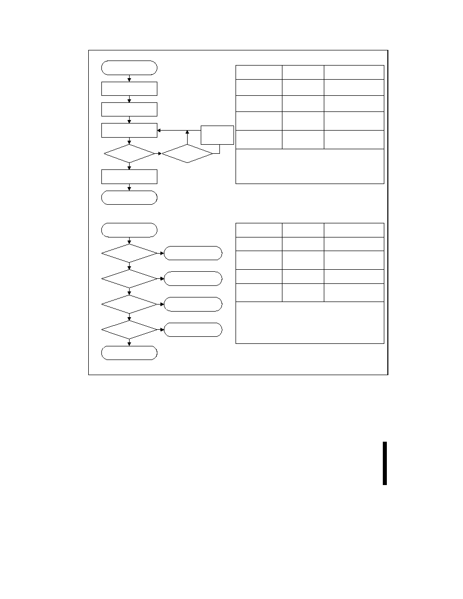
Figure 7. Automated Word Programming Flowchart

E
SMART 3 ADVANCED BOOT BLOCK≠WORD-WIDE
23
PRELIMINARY
Start
Write B0H
Read Status Register
Bus Operation
Write
Write
No
Command
Program Suspend
Read Array
Comments
Data = B0H
Addr = X
Data = FFH
Addr = X
SR.7 =
SR.2 =
1
Write FFH
Read Array Data
Program Completed
Done
Reading
Yes
Write FFH
Write D0H
Program Resumed
Read Array Data
0
1
0
Read
Read array data from block
other than the one being
programmed.
Read
Status Register Data Toggle
CE# or OE# to Update Status
Register Data
Addr = X
Standby
Check SR.7
1 = WSM Ready
0 = WSM Busy
Standby
Check SR.2
1 = Program Suspended
0 = Program Completed
Write
Program Resume
Data = D0H
Addr = X
0580_08
Figure 8. Program Suspend/Resume Flowchart
SMART 3 ADVANCED BOOT BLOCK≠WORD-WIDE
E
24
PRELIMINARY
Start
Write 20H
Write D0H and
Block Address
Read Status Register
SR.7 =
Full Status
Check if Desired
Block Erase Complete
FULL STATUS CHECK PROCEDURE
Bus Operation
Write
Write
Standby
Repeat for subsequent block erasures.
Full Status Check can be done after each block erase or after a sequence of
block erasures.
Write FFH after the last write operation to reset device to read array mode.
Bus Operation
Standby
SR. 1 and 3 MUST be cleared, if set during an erase attempt, before further
attempts are allowed by the Write State Machine.
SR.1, 3, 4, 5 are only cleared by the Clear Staus Register Command, in cases
where multiple bytes are erased before full status is checked.
If an error is detected, clear the status register before attempting retry or other
error recovery.
No
Yes
Suspend Erase
Suspend
Erase Loop
1
0
Standby
Command
Erase Setup
Erase Confirm
Comments
Data = 20H
Addr = Within Block to Be
Erased
Data = D0H
Addr = Within Block to Be
Erased
Check SR.7
1 = WSM Ready
0 = WSM Busy
Command
Comments
Check SR.3
1 = V
PP
Low Detect
Check SR.4,5
Both 1 = Command Sequence
Error
Read Status Register
Data (See Above)
V
PP
Range Error
Command Sequence
Error
Block Erase
Successful
SR.3 =
SR.4,5 =
1
0
1
0
Block Erase Error
SR.5 =
1
0
Attempted Erase of
Locked Block - Aborted
SR.1 =
1
0
Read
Status Register Data Toggle
CE# or OE# to Update Status
Register Data
Standby
Check SR.5
1 = Block Erase Error
Standby
Check SR.1
1 = Attempted Erase of
Locked Block - Erase Aborted
0580_09
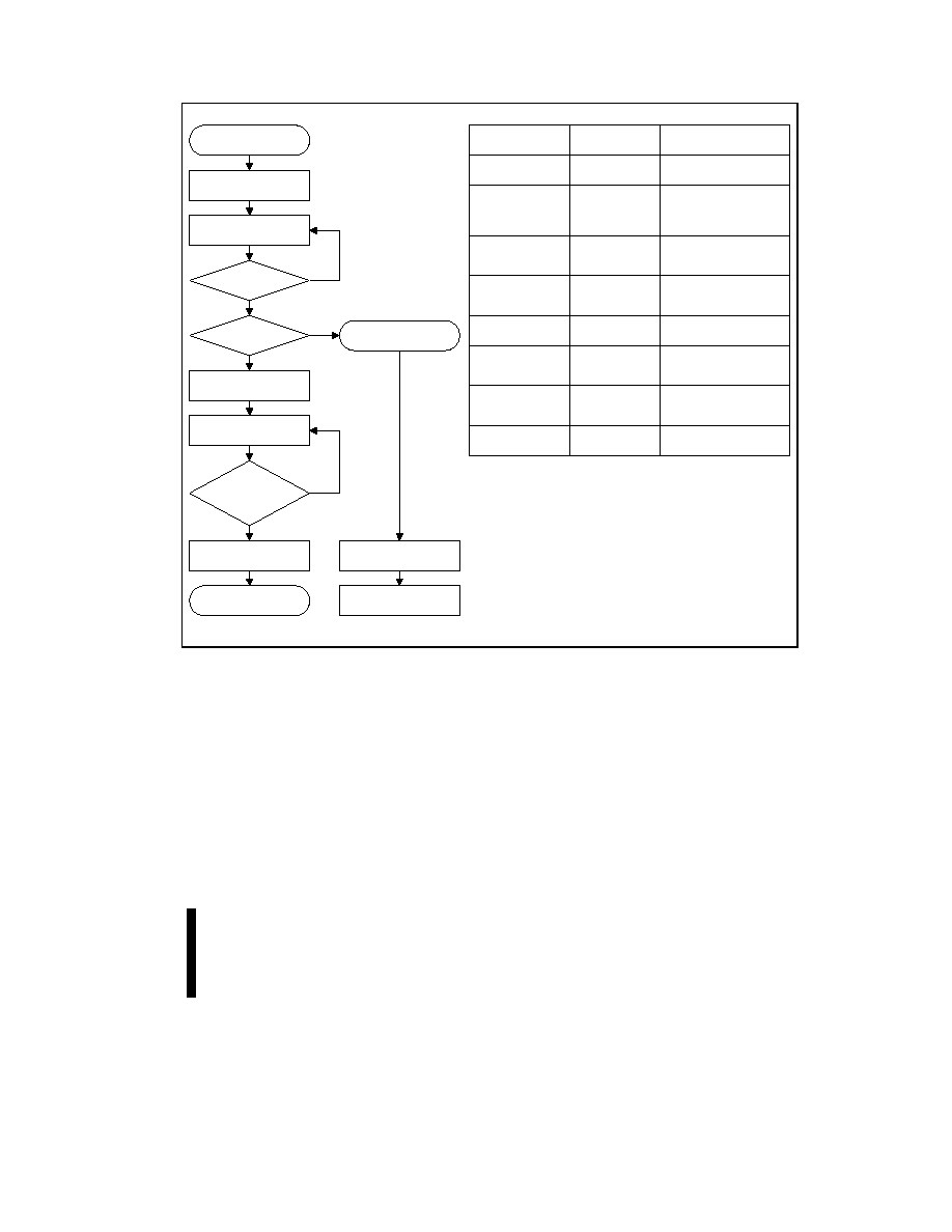
Figure 9. Automated Block Erase Flowchart
E
SMART 3 ADVANCED BOOT BLOCK≠WORD-WIDE
25
PRELIMINARY
Start
Write B0H
Read Status Register
Bus Operation
Write
Write
No
Command
Erase Suspend
Read Array
Comments
Data = B0H
Addr = X
Data = FFH
Addr = X
SR.7 =
SR.6 =
1
Write FFH/40H
Read Array Data/
Program Array
Erase Completed
Done
Reading and/or
Programming
Yes
Write FFH
Write D0H
Erase Resumed
Read Array Data
0
1
0
Read
Read array data from block
other than the one being
erased.
Read
Status Register Data Toggle
CE# or OE# to Update Status
Register Data
Addr = X
Standby
Check SR.7
1 = WSM Ready
0 = WSM Busy
Standby
Check SR.6
1 = Erase Suspended
0 = Erase Completed
Write
Erase Resume
Data = D0H
Addr = X
Program
Program data to block other
than the one being erased.
0580_10
Figure 10. Erase Suspend/Resume Flowchart

SMART 3 ADVANCED BOOT BLOCK≠WORD-WIDE
E
26
PRELIMINARY
3.3
Block Locking
The Smart 3 Advanced Boot Block flash memory
architecture features two hardware-lockable
parameter blocks so that the kernel code for the
system can be kept secure while other parameter
blocks are programmed or erased as necessary.
3.3.1
V
PP
= V
IL
FOR COMPLETE
PROTECTION
The V
PP
programming voltage can be held low for
complete write protection of all blocks in the flash
device. When V
PP
is below V
PPLK
, any program or
erase operation will result in a error, prompting the
corresponding Status Register bit (SR.3) to be set.
3.3.2
WP# = V
IL
FOR BLOCK LOCKING
The lockable blocks are locked when WP# = V
IL
;
any program or erase operation to a locked block
will result in an error, which will be reflected in the
status register. For top configuration, the top two
parameter blocks (blocks #37 and #38 for the
16-Mbit, blocks #21 and #22 for the 8-Mbit, and
blocks #13 and #14 for the 4-Mbit) are lockable. For
the bottom configuration, the bottom two parameter
blocks (blocks #0 and #1 for 4-/8-/16-Mbit) are
lockable. Unlocked blocks can be programmed or
erased normally (unless V
PP
is below V
PPLK
).
3.3.3
WP# = V
IH
FOR BLOCK UNLOCKING
WP# = V
IH
unlocks all lockable blocks.
These blocks can now be programmed or erased.
Note that RP# does not override WP# locking as in
previous Boot Block devices. WP# controls all block
locking and V
PP
provides protection against
spurious writes. Table 8 defines the write protection
methods.
3.4
V
PP
Program and Erase
Voltages
Intel's Smart 3 products provide in-system
programming and erase at 2.7V≠3.6V V
PP
. For
customers requiring fast programming in their
manufacturing environment, Smart 3 includes an
additional low-cost, backward-compatible 12V
programming feature.
The 12V V
PP
mode enhances programming
performance during the short period of time typically
found in manufacturing processes; however, it is
not intended for extended use. 12V may be applied
to V
PP
during program and erase operations for a
maximum of 1000 cycles on the main blocks and
2500 cycles on the parameter blocks. V
PP
may be
connected to 12V for a total of 80 hours maximum.
Stressing the device beyond these limits may cause
permanent damage.
Table 8. Write Protection Truth Table for
Advanced Boot Block Flash Memory Family
V
PP
WP#
RP#
Write Protection
Provided
X
X
V
IL
All Blocks Locked
V
IL
X
V
IH
All Blocks Locked
V
PPLK
V
IL
V
IH
Lockable Blocks
Locked
V
PPLK
V
IH
V
IH
All Blocks Unlocked
3.5
Power Consumption
While in operation, the flash device consumes
active power. However, Intel Flash devices have a
three-tiered approach to power savings that can
significantly reduce overall system power
consumption. The Automatic Power Savings (APS)
feature reduces power consumption when the
device is idle. If the CE# is deasserted, the flash
enters its standby mode, where current
consumption is even lower. If RP# = V
IL
the flash
enters a deep power-down mode, where current is
at a minimum. The combination of these features
can minimize overall memory power consumption,
and therefore, overall system power consumption.
3.5.1
ACTIVE POWER
With CE# at a logic-low level and RP# at a logic-
high level, the device is in the active mode. Refer to
the DC Characteristics tables for I
CC
current values.
Active power is the largest contributor to overall
system power consumption. Minimizing the active
current could have a profound effect on system
power consumption, especially for battery-operated
devices.

E
SMART 3 ADVANCED BOOT BLOCK≠WORD-WIDE
27
PRELIMINARY
3.5.2
AUTOMATIC POWER SAVINGS (APS)
Automatic Power Savings provides low-power
operation during active mode. Power Reduction
Control (PRC) circuitry allows the flash to put itself
into a low current state when not being accessed.
After data is read from the memory array, PRC
logic controls the device's power consumption by
entering the APS mode where typical I
CC
current is
comparable to I
CCS
. The flash stays in this static
state with outputs valid until a new location is read.
APS reduces active current to standby current
levels for 2.7V≠3.6V CMOS input levels.
3.5.3
STANDBY POWER
With CE# at a logic-high level (V
IH
) and the CUI in
read mode, the flash memory is in standby mode,
which disables much of the device's circuitry and
substantially reduces power consumption. Outputs
(DQ
0
≠DQ
15
) are placed in a high-impedance state
independent of the status of the OE# signal. If CE#
transitions to a logic-high level during erase or
program operations, the device will continue to
perform the operation and consume corresponding
active power until the operation is completed.
System engineers should analyze the breakdown of
standby time versus active time and quantify the
respective power consumption in each mode for
their specific application. This will provide a more
accurate measure of application-specific power and
energy requirements.
3.5.4
DEEP POWER-DOWN MODE
The deep power-down mode of the Smart 3
Advanced Boot Block products switches the device
into a low power savings mode, which is especially
important for battery-based devices. This mode is
activated when RP# = V
IL
(GND
±
0.2V).
During read modes, RP# going low de-selects the
memory and places the output drivers in a high
impedance state. Recovery from the deep power-
down state, requires a minimum time equal to t
PHQV
(see AC Characteristics table).
During program or erase modes, RP# transitioning
low will abort the operation, but the memory
contents of the address being programmed or the
block being erased are no longer valid as the data
integrity has been compromised by the abort.
During deep power-down, all internal circuits are
switched to a low power savings mode (RP#
transitioning to V
IL
or turning off power to the device
clears the status register).
3.6
Power-Up/Down Operation
The device is protected against accidental block
erasure or programming during power transitions.
Power supply sequencing is not required, since
the
device is indifferent as to which power supply, V
PP
or V
CC
, powers-up first.
3.6.1
RP# CONNECTED TO SYSTEM
RESET
The use of RP# during system reset is important
with automated program/erase devices since the
system expects to read from the flash memory
when it comes out of reset. If a CPU reset occurs
without a flash memory reset, proper CPU
initialization will not occur because the flash
memory may be providing status information
instead of array data. Intel recommends connecting
RP# to the system CPU RESET# signal to allow
proper CPU/flash initialization following system
reset.
System designers must guard against spurious
writes when V
CC
voltages are above V
LKO
and V
PP
is active. Since both WE# and CE# must be low for
a command write, driving either signal to V
IH
will
inhibit writes to the device. The CUI architecture
provides additional protection since alteration of
memory contents can only occur after successful
completion of the two-step command sequences.
The device is also disabled until RP# is brought to
V
IH
, regardless of the state of its control inputs. By
holding the device in reset (RP# connected to
system PowerGood) during power-up/down, invalid
bus conditions during power-up can be masked,
providing yet another level of memory protection.
3.6.2
V
CC
, V
PP
AND RP# TRANSITIONS
The CUI latches commands as issued by system
software and is not altered by V
PP
or CE#
transitions or WSM actions. Its default state upon
power-up, after exit from deep power-down mode or
after V
CC
transitions above V
LKO
(Lockout voltage),
is read array mode.

SMART 3 ADVANCED BOOT BLOCK≠WORD-WIDE
E
28
PRELIMINARY
After any program or block erase operation is
complete (even after V
PP
transitions down to
V
PPLK
), the CUI must be reset to read array mode
via the Read Array command if access to the flash
memory array is desired.
Refer to
AP-617 Additional Flash Data Protection
Using V
PP
, RP#, and WP# for a circuit-level
description of how to implement the protection
schemes discussed in Section 3.5.
3.7
Power Supply Decoupling
Flash memory's power switching characteristics
require careful device decoupling. System
designers should consider three supply current
issues:
1.
Standby current levels (I
CCS
)
2.
Active current levels (I
CCR
)
3.
Transient peaks produced by falling and rising
edges of CE#.
Transient current magnitudes depend on the device
outputs' capacitive and inductive loading. Two-line
control and proper decoupling capacitor selection
will suppress these transient voltage peaks. Each
flash device should have a 0.1 µF ceramic
capacitor connected between each V
CC
and GND,
and between its V
PP
and GND. These high-
frequency, inherently low-inductance capacitors
should be placed as close as possible to the
package leads.
3.7.1
V
PP
TRACE ON PRINTED CIRCUIT
BOARDS
Designing for in-system writes to the flash memory
requires special consideration of the V
PP
power
supply trace by the printed circuit board designer.
The V
PP
pin supplies the flash memory cells current
for programming and erasing. V
PP
trace widths and
layout should be similar to that of V
CC
. Adequate
V
PP
supply traces, and decoupling capacitors
placed adjacent to the component, will decrease
spikes and overshoots.
E
SMART 3 ADVANCED BOOT BLOCK≠WORD-WIDE
29
PRELIMINARY
4.0
ABSOLUTE MAXIMUM
RATINGS*
Extended Operating Temperature
During Read ............................ ≠40∞C to +85∞C
During Block Erase
and Program............................ ≠40∞C to +85∞C
Temperature Under Bias ......... ≠40∞C to +85∞C
Storage Temperature................... ≠65∞C to +125∞C
Voltage on Any Pin
(except V
CC
, V
CCQ
and V
PP
)
with Respect to GND ............... ≠0.5V to +5.0V
1
V
PP
Voltage (for Block
Erase and Program)
with Respect to GND .........≠0.5V to +13.5V
1,2,4
V
CC
and V
CCQ
Supply Voltage
with Respect to GND ............... ≠0.2V to +5.0V
1
Output Short Circuit Current...................... 100 mA
3
NOTICE: This datasheet contains preliminary information on
new products in production. Do not finalize a design with
this information. Revised information will be published when
the product is available. Verify with your local Intel Sales
office that you have the latest data sheet before finalizing a
design.
* WARNING: Stressing the device beyond the "Absolute
Maximum Ratings" may cause permanent damage. These
are stress ratings only. Operation beyond the "Operating
Conditions" is not recommended and extended exposure
beyond the "Operating Conditions" may effect device
reliability.
NOTES:
1.
Minimum DC voltage is ≠0.5V on input/output pins.
During transitions, this level may undershoot to ≠2.0V
for periods < 20 ns. Maximum DC voltage on
input/output pins is V
CC
+ 0.5V which, during
transitions, may overshoot to V
CC
+ 2.0V for periods <
20 ns.
2.
Maximum DC voltage on V
PP
may overshoot to +14.0V
for periods < 20 ns.
3.
Output shorted for no more than one second. No more
than one output shorted at a time.
4.
V
PP
Program voltage is normally 2.7V≠3.6V.
Connection to supply of 11.4V≠12.6V can only be done
for 1000 cycles on the main blocks and 2500 cycles on
the parameter blocks during program/erase. V
PP
may
be connected to 12V for a total of 80 hours maximum.
See Section 3.4 for details.
5.0
OPERATING CONDITIONS (V
CCQ
= 2.7V≠3.6V)
Table 9. Temperature and Voltage Operating Conditions4
Symbol
Parameter
Notes
Min
Max
Units
T
A
Operating Temperature
≠40
+85
∞C
V
CC
2.7V≠3.6V V
CC
Supply Voltage
1,4
2.7
3.6
Volts
V
CCQ
2.7V≠3.6V I/O Supply Voltage
1,2,4
2.7
3.6
Volts
V
PP1
Program and Erase Voltage
4
2.7
3.6
Volts
V
PP2
3
11.4
12.6
Volts
Cycling
Block Erase Cycling
5
10,000
Cycles
NOTES:
1.
See DC Characteristics tables for voltage range-specific specifications.
2.
The voltage swing on the inputs, V
IN
is required to match V
CCQ
.
3.
Applying V
PP
= 11.4V≠12.6V during a program/erase can only be done for a maximum of 1000 cycles on the main blocks
and 2500 cycles on the parameter blocks. V
PP
may be connected to 12V for a total of 80 hours maximum. See Section 3.4
for details.
4.
V
CC
, V
CCQ
and V
PP1
must share the same supply when all three are between 2.7V and 3.6V.
5.
For operating temperatures of ≠25
∞
C≠ +85
∞
C the device is projected to have a minimum block erase cycling of 10,000 to
30,000 cycles.

SMART 3 ADVANCED BOOT BLOCK≠WORD-WIDE
E
30
PRELIMINARY
5.1
DC Characteristics: V
CCQ
= 2.7V≠3.6V
Table 10. DC Characteristics
Sym
Parameter
Notes
V
CC
= 2.7V≠3.6V
Unit
Test Conditions
Typ
Max
I
LI
Input Load Current
1
± 1.0
µA
V
CC
= V
CC
Max = V
CCQ
Max
V
IN
= V
CCQ
or GND
I
LO
Output Leakage Current
1
± 10
µA
V
CC
= V
CC
Max = V
CCQ
Max
V
IN
= V
CCQ
or GND
I
CCS
V
CC
Standby Current
1,7
20
50
µA
CMOS INPUTS
V
CC
= V
CC
Max = V
CCQ
Max
CE# = RP# = V
CCQ
I
CCD
V
CC
Deep Power-Down
Current
1,7
1
10
µA
CMOS INPUTS
V
CC
= V
CC
Max = V
CCQ
Max
V
IN
= V
CCQ
or GND
RP# = GND ± 0.2V
I
CCR
V
CC
Read Current
1,5,7
10
20
mA
CMOS INPUTS
V
CC
= V
CC
Max = V
CCQ
Max
OE# = V
IH
, CE# =V
IL
f = 5 MHz,
I
OUT
= 0 mA
Inputs = V
IL
or V
IH
I
CCW
V
CC
Program Current
1,4,7
8
20
mA
V
PP
= V
PPH1
(3V)
Program in Progress
8
20
mA
V
PP
= V
PPH2
(12V)
Program in Progress
I
CCE
V
CC
Erase Current
1,4,7
8
20
mA
V
PP
= V
PPH1
(3V)
Erase in Progress
8
20
mA
V
PP
= V
PPH2
(12V)
Erase in Progress
I
CCES
V
CC
Erase Suspend
Current
1,2,4,7
20
50
µA
CE# = V
IH
Erase Suspend in Progress
I
CCWS
V
CC
Program Suspend
Current
1,2,4,7
20
50
µA
CE# = V
IH
Program Suspend in Progress
I
PPD
V
PP
Deep Power-Down
Current
1
0.2
5
µA
RP# = GND ± 0.2V
I
PPR
V
PP
Read Current
1
2
±50
µA
V
PP
V
CC

E
SMART 3 ADVANCED BOOT BLOCK≠WORD-WIDE
31
PRELIMINARY
Table 10. DC Characteristics (Continued)
Sym
Parameter
Notes
V
CC
= 2.7V≠3.6V
Unit
Test Conditions
Typ
Max
I
PPW
V
PP
Program Current
1,4
15
40
mA
V
PP
= V
PPH1
(3V)
Program in Progress
10
25
mA
V
PP
= V
PPH2
(12V)
Program in Progress
I
PPE
V
PP
Erase Current
1,4
13
25
mA
V
PP
= V
PPH1
(3V)
Erase in Progress
8
25
mA
V
PP
= V
PPH2
(12V)
Erase in Progress
I
PPES
V
PP
Erase Suspend
Current
1,4
50
200
µA
V
PP
= V
PPH1
or V
PPH2
Erase Suspend in Progress
I
PPWS
V
PP
Program Suspend
Current
1,4
50
200
µA
V
PP
= V
PPH1
or V
PPH2
Program Suspend in Progress

SMART 3 ADVANCED BOOT BLOCK≠WORD-WIDE
E
32
PRELIMINARY
Table 10. DC Characteristics (Continued)
Sym
Parameter
Notes
V
CC
= 2.7V≠3.6V
Unit
Test Conditions
Min
Max
V
IL
Input Low Voltage
≠0.4
0.4
V
V
IH
Input High Voltage
V
CCQ
≠
0.4V
V
V
OL
Output Low Voltage
0.10
V
V
CC
= V
CC
Min = V
CCQ
Min
I
OL
= 100
µ
A
V
OH
Output High Voltage
V
CCQ
≠
0.1V
V
V
CC
= V
CC
Min
= V
CCQ
Min
I
OH
= ≠100
µ
A
V
PPLK
V
PP
Lock-Out Voltage
3
1.5
V
Complete Write Protection
V
PPH1
V
PP
during Prog/Erase
Operations
3
2.7
3.6
V
V
PPH2
3,6
11.4
12.6
V
V
LKO
V
CC
Program/Erase Lock
Voltage
1.5
V
V
LKO2
V
CCQ
Program/Erase
Lock Voltage
1.2
V
NOTES:
1.
All currents are in RMS unless otherwise noted. Typical values at nominal V
CC
, T
A
= +25∞C.
2.
I
CCES
and I
CCWS
are specified with device de-selected. If device is read while in erase suspend, current draw is sum of
I
CCES
and I
CCR
. If the device is read while in program suspend, current draw is the sum of I
CCWA
and I
CCR
.
3.
Erase and Program are inhibited when V
PP
< V
PPLK
and not guaranteed outside the valid V
PP
ranges of V
PPH1
and V
PPH2
.
4.
Sampled, not 100% tested.
5.
Automatic Power Savings (APS) reduces I
CCR
to approximately standby levels in static operation (CMOS inputs).
6.
Applying V
PP
= 11.4V≠12.6V during program/erase can only be done for a maximum of 1000 cycles on the main blocks
and 2500 cycles on the parameter blocks. V
PP
may be connected to 12V for a total of 80 hours maximum. See Section 3.4
for details.
7.
Includes the sum of V
CC
and V
CCQ
current.
Table 11. Capacitance (T
A
= 25∞C, f = 1 MHz)
Sym
Parameter
Notes
Typ
Max
Units
Conditions
C
IN
Input Capacitance
1
6
8
pF
V
IN
= 0V
C
OUT
Output Capacitance
1
10
12
pF
V
OUT
= 0V
NOTE:
1.
Sampled, not 100% tested.
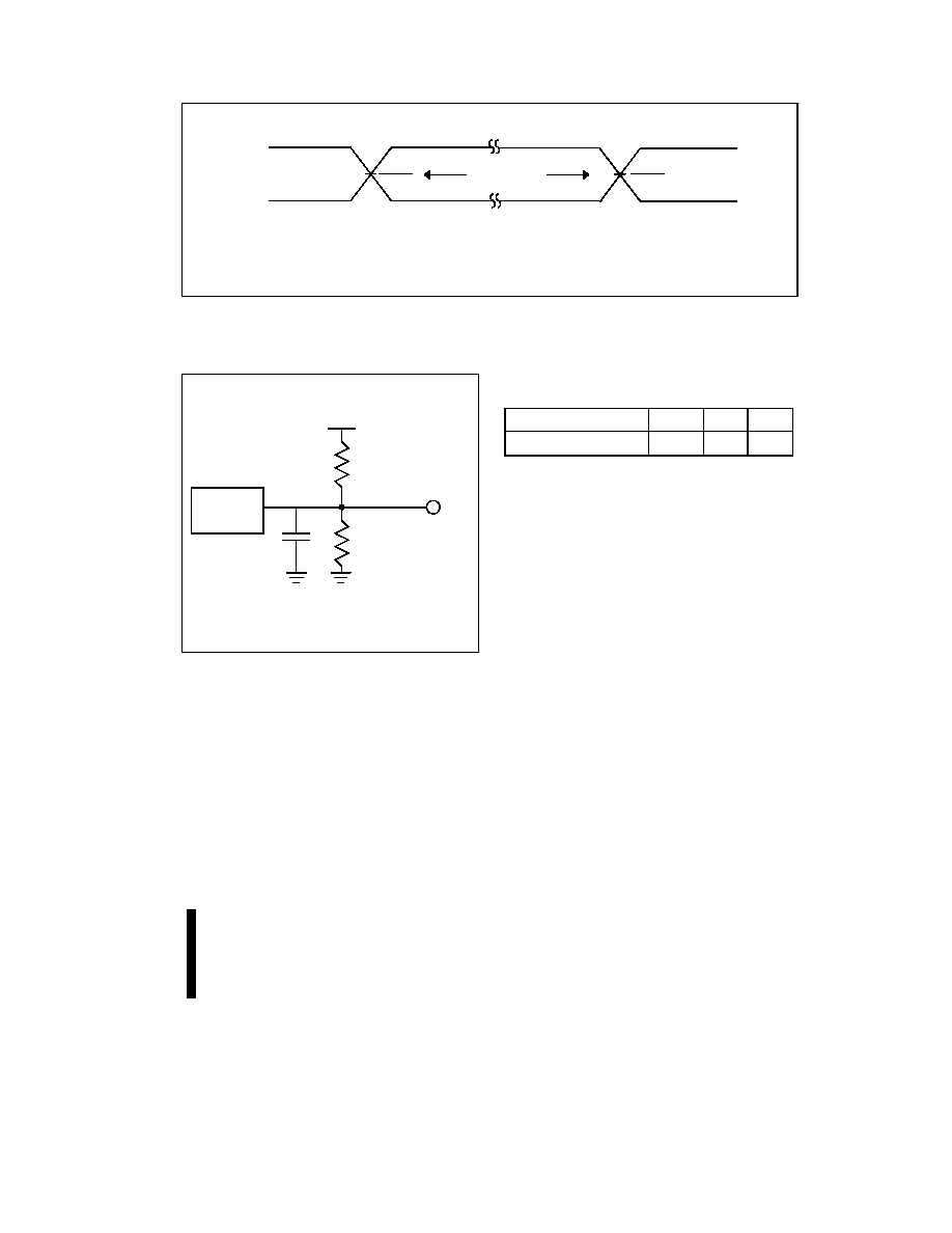
E
SMART 3 ADVANCED BOOT BLOCK≠WORD-WIDE
33
PRELIMINARY
TEST POINTS
INPUT
OUTPUT
V
CCQ
0.0
V
CCQ
2
V
CCQ
2
0580_11
NOTE:
AC test inputs are driven at V
CCQ
for a logic "1" and 0.0V for a logic "0." Input timing begins, and output timing ends, at V
CCQ
/2.
Input rise and fall times (10%≠90%) <10 ns. Worst case speed conditions are when V
CCQ
= 2.7V.
Figure 11. 2.7V≠3.6V Input Range and Measurement Points
C
L
Out
V
CCQ
Device
under
Test
R
1
R
2
0580_12
NOTE:
See table for component values.
Figure 12. Test Configuration
Test Configuration Component Values for Worst
Case Speed Conditions
Test Configuration
C
L
(pF) R
1
(
) R
2
(
)
2.7V Standard Test
50
25K
25K
NOTE:
C
L
includes jig capacitance.

SMART 3 ADVANCED BOOT BLOCK≠WORD-WIDE
E
34
PRELIMINARY
6.0
OPERATING CONDITIONS (V
CCQ
= 1.8V≠2.2V)
Table 12. Temperature and V
CC
Operating Conditions
Symbol
Parameter
Notes
Min
Max
Units
T
A
Operating Temperature
≠40
+85
∞C
V
CC1
2.7V≠2.85V V
CC
Supply Voltage
1
2.7
2.85
Volts
V
CC2
2.7V≠3.3V V
CC
Supply Voltage
1
2.7
3.3
Volts
V
CCQ
1.8V≠2.2V I/O Supply Voltage
1,4
1.8
2.2
Volts
V
PP1
Program and Erase Voltage
1
2.7
2.85
Volts
V
PP2
1
2.7
3.3
Volts
V
PP3
1,2
11.4
12.6
Volts
Cycling
Block Erase Cycling
3
10,000
Cycles
NOTES:
1.
See DC Characteristics tables for voltage range-specific specifications.
2.
Applying V
PP
= 11.4V≠12.6V during program/erase can only be done for a maximum of 1000 cycles on the main blocks
and 2500 cycles on the parameter. V
PP
may be connected to 12V for a total of 80 hours maximum. See Section 3.4 for
details.
3.
For operating temperatures of ≠25
∞
C≠ +85
∞
C the device is projected to have a minimum block erase cycling of 10,000 to
30,000 cycles.
4.
The voltage swing on the inputs, V
IN
is required to match V
CCQ
.
6.1
DC Characteristics: V
CCQ
= 1.8V≠2.2V
These tables are valid for the following power supply combinations only:
1.
V
CC1
and V
CCQ
and (V
PP1
or V
PP3
)
2.
V
CC2
and V
CCQ
and (V
PP2
or V
PP3
)
Wherever the input voltage V
IN
is mentioned, it is required that V
IN
matches the chosen V
CCQ
.

E
SMART 3 ADVANCED BOOT BLOCK≠WORD-WIDE
35
PRELIMINARY
Table 13. DC Characteristics: V
CCQ
= 1.8V≠2.2V
Sym
Parameter
Notes
V
CC1
:
2.7V≠2.85V
V
CC2
:
2.7V≠3.3V
Unit
Test Conditions
Typ
Max
I
LI
Input Load Current
1
± 1.0
µA
V
CC
= V
CC
Max
V
CCQ
= V
CCQ
Max
V
IN
= V
CCQ
or GND
I
LO
Output Leakage Current
1
± 10
µA
V
CC
= V
CC
Max
V
CCQ
=
V
CCQ
Max
V
IN
= V
CCQ
or GND
I
CCS
V
CC
Standby Current
1,7
20
50
µA
CMOS INPUTS
V
CC
= V
CC1
Max (2.7V≠2.85V)
V
CCQ
= V
CCQ
Max
CE# = RP# = V
CCQ
150
250
µ
A
CMOS INPUTS
V
CC
= V
CC2
Max (2.7V≠3.3V)
V
CCQ
= V
CCQ
Max
CE# = RP# = V
CCQ
I
CCD
V
CC
Deep Power-Down
Current
1,7
1
10
µA
CMOS INPUTS
V
CC
= V
CC
Max (V
CC1
or V
CC2
)
V
CCQ
= V
CCQ
Max
V
IN
= V
CCQ
or GND
RP# = GND ± 0.2V
I
CCR
V
CC
Read Current
1,5,7
8
18
mA
CMOS INPUTS
V
CC
= V
CC1
Max (2.7V≠2.85V)
V
CCQ
= V
CCQ
Max
OE# = V
IH
, CE# = V
IL
f = 5 MHz, I
OUT
= 0 mA
Inputs = V
IL
or V
IH
12
23
mA
CMOS INPUTS
V
CC
= V
CC2
Max (2.7V≠3.3V)
V
CCQ
= V
CCQ
Max
OE# = V
IH
, CE# = V
IL
f = 5 MHz, I
OUT
= 0 mA
Inputs = GND ± 0.2V or V
CCQ

SMART 3 ADVANCED BOOT BLOCK≠WORD-WIDE
E
36
PRELIMINARY
Table 13. DC Characteristics: V
CCQ
= 1.8V≠2.2V (Continued)
Sym
Parameter
Notes
V
CC1
:
2.7V≠2.85V
V
CC2
:
2.7V≠3.3V
Unit
Test Conditions
Typ
Max
I
CCW
V
CC
Program Current
1,4,7
8
20
mA
V
PP
= V
PPH1
or V
PPH2
Program in Progress
8
20
mA
V
PP
= V
PPH3
(12V)
Program in Progress
I
CCE
V
CC
Erase Current
1,4,7
8
20
mA
V
PP
= V
PPH1
or V
PPH2
Erase in Progress
8
20
mA
V
PP
= V
PPH3
(12V)
Erase in Progress
I
CCES
V
CC
Erase Suspend
Current
1,2,4,7
20
50
µA
CE# = V
IH
Erase Suspend in Progress
I
CCWS
V
CC
Program Suspend
Current
1,2,4,7
20
50
µA
CE# = V
IH
Program Suspend in Progress
I
PPD
V
PP
Deep Power-Down
Current
1
0.2
5
µA
RP# = GND ± 0.2V
I
PPR
V
PP
Read and Standby
Current
1
2
±50
µA
V
PP
V
CC
I
PPW
V
PP
Program Current
1,4
15
40
mA
V
PP
= V
PPH1
or V
PPH2
Program in Progress
10
25
mA
V
PP
= V
PPH3
(12V)
Program in Progress
I
PPE
V
PP
Erase Current
1,4
13
25
mA
V
PP
= V
PPH1
or V
PPH2
Erase in Progress
8
25
mA
V
PP
= V
PPH3
(12V)
Erase in Progress
I
PPES
V
PP
Erase Suspend
Current
1
50
200
µA
V
PP
= V
PPH1
, V
PPH2
, or V
PPH3
Erase Suspend in Progress
I
PPWS
V
PP
Program Suspend
Current
1
50
200
µA
V
PP
= V
PPH1
, V
PPH2
, or V
PPH3
Program Suspend in Progress
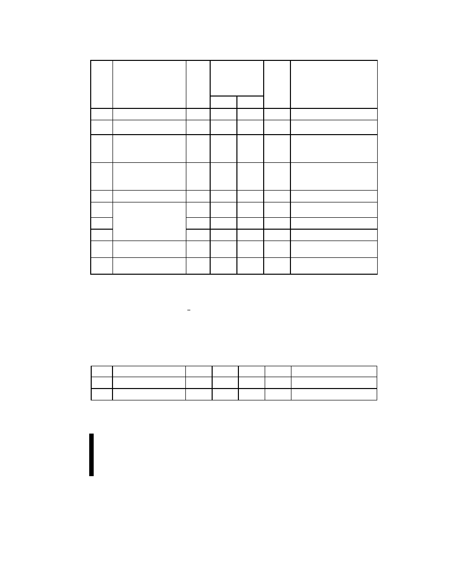
E
SMART 3 ADVANCED BOOT BLOCK≠WORD-WIDE
37
PRELIMINARY
Table 13. DC Characteristics: V
CCQ
= 1.8V≠2.2V (Continued)
Sym
Parameter
Notes
V
CC1
:
2.7V≠2.85V
V
CC2
:
2.7V≠3.3V
Unit
Test Conditions
Min
Max
V
IL
Input Low Voltage
≠0.2
0.2
V
V
IH
Input High Voltage
V
CCQ
≠
0.2V
V
V
OL
Output Low Voltage
≠0.10
0.10
V
V
CC
= V
CC
Min
V
CCQ
= V
CCQ
Min
I
OL
= 100
µ
A
V
OH
Output High Voltage
V
CCQ
≠
0.1V
V
V
CC
= V
CC
Min
V
CCQ
= V
CCQ
Min
I
OL
= ≠100
µ
A
V
PPLK
V
PP
Lock-Out Voltage
3
1.5
V
Complete Write Protection
V
PPH1
V
PP
during Program/
Erase Operations
3
2.7
2.85
V
V
PPH2
3
2.7
3.3
V
V
PPH3
3,6
11.4
12.6
V
V
LKO1
V
CC
Program/Erase Lock
Voltage
1.5
V
V
LKO2
V
CCQ
Program/Erase
Lock Voltage
1.2
V
NOTES:
1.
All currents are in RMS unless otherwise noted. Typical values at nominal V
CC
, T
A
= +25∞C.
2.
I
CCES
and I
CCWS
are specified with device de-selected. If device is read while in erase suspend, current draw is I
CCR
. If the
device is read while in program suspend , current draw is I
CCR
.
3.
Erases and Writes inhibited when V
PP
< V
PPLK
, and not guaranteed outside the valid V
PP
ranges of V
PPH1
,V
PPH2
. or V
PPH3.
4.
Sampled, not 100% tested.
5.
Automatic Power Savings (APS) reduces I
CCR
to approximately standby levels in static operation (CMOS inputs).
6.
Applying V
PP
= 11.4V≠12.6V during program/erase can only be done for a maximum of 1000 cycles on the main blocks
and 2500 cycles on the parameter blocks. V
PP
may be connected to 12V for a total of 80 hours maximum. See Section 3.4
for details.
7
Includes the sum of V
CC
and V
CCQ
current
Table 14. Capacitance (T
A
= 25∞C, f = 1 MHz)
Sym
Parameter
Notes
Typ
Max
Units
Conditions
C
IN
Input Capacitance
1
6
8
pF
V
IN
= 0V
C
OUT
Output Capacitance
1
10
12
pF
V
OUT
= 0V
NOTE:
1.
Sampled, not 100% tested.
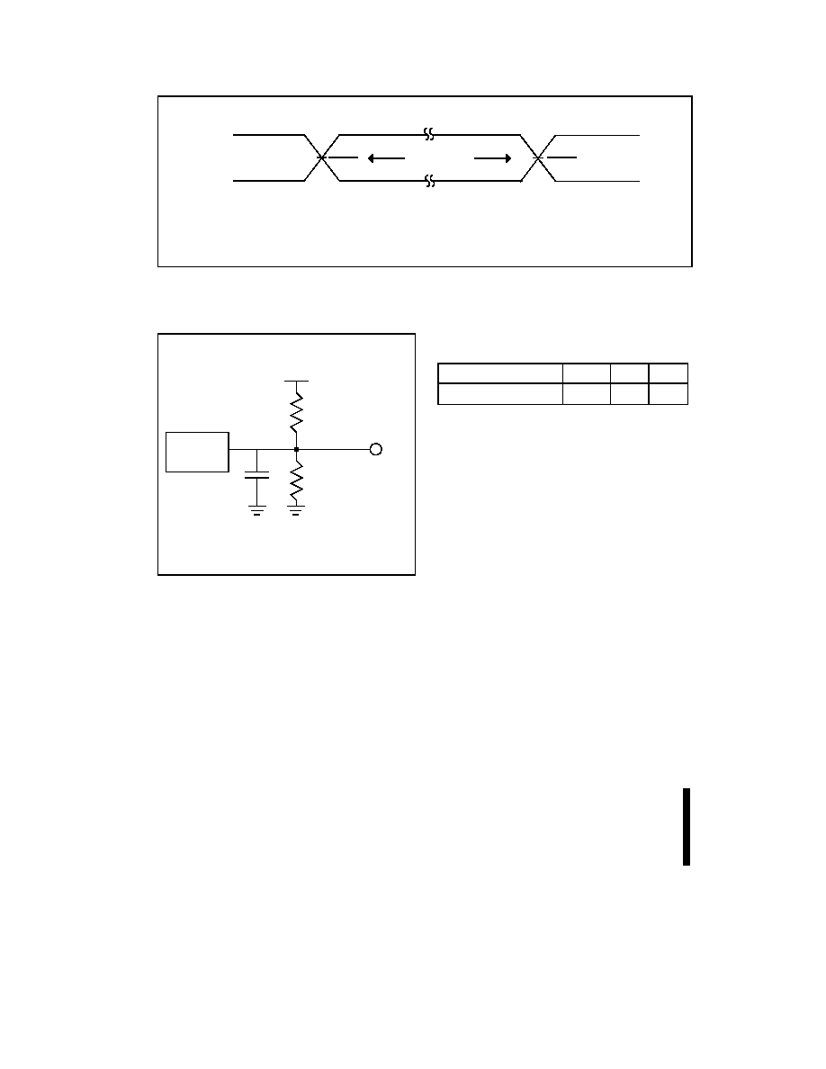
SMART 3 ADVANCED BOOT BLOCK≠WORD-WIDE
E
38
PRELIMINARY
TEST POINTS
INPUT
OUTPUT
V
CCQ
0.0
V
CCQ
2
V
CCQ
2
0580_11
NOTE:
AC test inputs are driven at V
CCQ
for a logic "1" and 0.0V for a logic "0." Input timing begins, and output timing ends, at V
CCQ
/2.
Input rise and fall times (10%≠90%) <10 ns. For worst case speed conditions V
CCQ
= 1.8V.
Figure 13. 1.8V--2.2V Input Range and Measurement Points
C
L
Out
V
CCQ
Device
under
Test
R
1
R
2
0580_12
NOTE:
See table for component values.
Figure 14. Test Configuration
Test Configuration Component Values for Worst
Case Speed Conditions
Test Configuration
C
L
(pF) R
1
(
) R
2
(
)
1.8V Standard Test
50
16.7K
16.7K
NOTE:
C
L
includes jig capacitance.

E
SMART 3 ADVANCED BOOT BLOCK≠WORD-WIDE
39
PRELIMINARY
7.0
AC CHARACTERISTICS
AC Characteristics are applicable to both V
CCQ
ranges.
Table 15. AC Characteristics: Read Operations (Extended Temperature)
Load
C
L
= 50 pF
#
Symbol
Parameter
V
CC
2.7V≠3.6V
4
Units
Prod
120 ns
150 ns
Notes
Min
Max
Min
Max
R1
t
AVAV
Read Cycle Time
120
150
ns
R2
t
AVQV
Address to Output Delay
120
150
ns
R3
t
ELQV
CE# to Output Delay
2
120
150
ns
R4
t
GLQV
OE# to Output Delay
2
65
65
ns
R5
t
PHQV
RP# to Output Delay
600
600
ns
R6
t
ELQX
CE# to Output in Low Z
3
0
0
ns
R7
t
GLQX
OE# to Output in Low Z
3
0
0
ns
R8
t
EHQZ
CE# to Output in High Z
3
40
40
ns
R9
t
GHQZ
OE# to Output in High Z
3
40
40
ns
R10
t
OH
Output Hold from Address, CE#,
or OE# Change, Whichever
Occurs First
3
0
0
ns
NOTES:
1.
See AC Input/Output Reference Waveform for timing measurements.
2.
OE# may be delayed up to t
ELQV
≠t
GLQV
after the falling edge of CE# without impact on t
ELQV
.
3.
Sampled, but not 100% tested.
4.
See Test Configuration (Figures 12 and 14), 2.7V≠3.6V and 1.8V≠2.2V Standard Test component values.
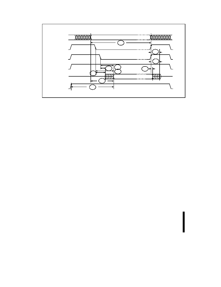
SMART 3 ADVANCED BOOT BLOCK≠WORD-WIDE
E
40
PRELIMINARY
Address Stable
Device and
Address Selection
IH
V
IL
V
ADDRESSES (A)
IH
V
IL
V
IH
V
IL
V
IH
V
IL
V
CE# (E)
OE# (G)
WE# (W)
DATA (D/Q)
IH
V
IL
V
RP#(P)
OL
V
OH
V
High Z
Valid Output
Data
Valid
Standby
High Z
R1
R2
R3
R4
R5
R6
R7
R8
R9
R10
0580_15
Figure 15. AC Waveform: Read Operations

E
SMART 3 ADVANCED BOOT BLOCK≠WORD-WIDE
41
PRELIMINARY
Table 16. AC Characteristics: Write Operations (Extended Temperature)
1
Load
50 pF
#
Symbol
Parameter
V
CC
2.7V≠3.6V
5
2.7V-3.6V
5
Units
Prod
120 ns
150 ns
Notes
Min
Max
Min
Max
W1
t
PHWL
t
PHEL
RP# High Recovery to
WE# (CE#) Going Low
600
600
ns
W2
t
ELWL
t
WLEL
CE# (WE#) Setup to
WE# (CE#) Going Low
0
0
ns
W3
t
WLWH
t
ELEH
WE# (CE#) Pulse Width
90
90
ns
W4
t
DVWH
t
DVEH
Data Setup to WE#
(CE#) Going High
3
70
70
ns
W5
t
AVWH
t
AVEH
Address Setup to WE#
(CE#) Going High
2
90
90
ns
W6
t
WHEH
t
EHWH
CE# (WE#) Hold Time
from WE# (CE#) High
0
0
ns
W7
t
WHDX
t
EHDX
Data Hold Time from
WE# (CE#) High
3
0
0
ns
W8
t
WHAX
t
EHAX
Address Hold Time from
WE# (CE#) High
2
0
0
ns
W9
t
WHWL
t
EHEL
WE# (CE#) Pulse Width
High
30
30
ns
W10
t
VPWH
t
VPEH
V
PP
Setup to WE# (CE#)
Going High
4
200
200
ns
W11
t
QVVL
V
PP
Hold from Valid SRD
4
0
0
ns
t
LOCK
Block Unlock / Lock
Delay
4, 6
200
200
ns
NOTES:
1.
Read timing characteristics during program suspend and erase suspend are the same as during read-only operations.
Refer to AC Characteristics during read mode.
2.
Refer to command definition table for valid A
IN
(Table 6).
3.
Refer to command definition table for valid D
IN
(Table 6).
4.
Sampled, but not 100% tested.
5.
See Test Configuration (Figures 12 and 14),
2.7V≠3.6V and 1.8V≠2.2V Standard Test component values.
6.
Time t
LOCK
is required for successful locking and unlocking of all lockable blocks.
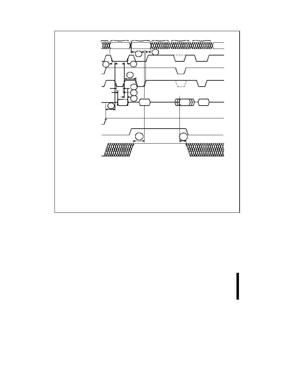
SMART 3 ADVANCED BOOT BLOCK≠WORD-WIDE
E
42
PRELIMINARY
ADDRESSES [A]
CE#(WE#) [E(W)]
OE# [G]
WE#(CE#) [W(E)]
DATA [D/Q]
RP# [P]
IH
V
IL
V
IH
V
IL
V
IH
V
IL
V
IH
V
IL
V
IL
V
IL
V
IN
D
IN
A
IN
A
Valid
SRD
IN
D
IH
V
High Z
IH
V
IL
V
V [V]
PP
PPH
V
PPLK
V
PPH
V
1
2
WP#
IL
V
IH
V
IN
D
A
B
C
D
E
F
W8
W6
W9
W3
W4
W7
W1
W5
W2
W10
W11
(Note 1)
(Note 1)
0580_16
NOTES:
1.
CE# must be toggled low when reading Status Register Data. WE# must be inactive (high) when reading Status Register
Data.
A.
V
CC
Power-Up and Standby.
B.
Write Program or Erase Setup Command.
C.
Write Valid Address and Data (for Program) or Erase Confirm Command.
D.
Automated Program or Erase Delay.
E.
Read Status Register Data (SRD): reflects completed program/erase operation.
F.
Write Read Array Command.
Figure 16. AC Waveform: Program and Erase Operations
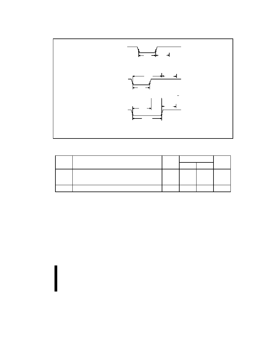
E
SMART 3 ADVANCED BOOT BLOCK≠WORD-WIDE
43
PRELIMINARY
7.1
Reset Operations
IH
V
IL
V
RP# (P)
PLPH
t
IH
V
IL
V
RP# (P)
PLPH
t
(A) Reset during Read Mode
Abort
Complete
PHQV
t
PHWL
t
PHEL
t
PHQV
t
PHWL
t
PHEL
t
(B) Reset during Program or Block Erase, <
PLPH
t
PLRH
t
PLRH
t
IH
V
IL
V
RP# (P)
PLPH
t
Abort
Complete
PHQV
t
PHWL
t
PHEL
t
PLRH
t
Deep
Power-
Down
(C) Reset Program or Block Erase, >
PLPH
t
PLRH
t
0580_17
Figure 17. AC Waveform: Deep Power-Down/Reset Operation
Reset Specifications
V
CC
= 2.7≠3.6V
Symbol
Parameter
Notes
Min
Max
Unit
t
PLPH
RP# Low to Reset during Read
(If RP# is tied to V
CC
, this specification is not
applicable)
1,3
100
ns
t
PLRH
RP# Low to Reset during Block Erase or Program
2,3
22
µs
NOTES:
1.
If t
PLPH
is < 100 ns the device may still RESET but this is not guaranteed.
2.
If RP# is asserted while a block erase or
word program operation is not executing, the reset will complete within 100 ns.
3. Sampled, but not 100% tested.

SMART 3 ADVANCED BOOT BLOCK≠WORD-WIDE
E
44
PRELIMINARY
Table 17. Erase and Program Timings
V
PP
= 2.7V
V
PP
= 12V
Sym
Parameter
Notes
Typ
1
Max
3
Typ
1
Max
3
Unit
t
BWPB
Block Program Time
(Parameter)
2
0.10
0.30
0.03
0.10
sec
t
BWMB
Block Program Time (Main)
2
0.80
2.40
0.24
0.80
sec
t
WHQV1
t
EHQV1
Program Time
2
22
200
8
185
µs
t
WHQV2
t
EHQV2
Block Erase Time (Parameter)
2
1
5.0
0.8
4.8
sec
t
WHQV3
t
EHQV3
Block Erase Time (Main)
2
1.8
8.0
1.1
7.0
sec
t
WHRH1
t
EHRH1
Program Suspend Latency
3
5
10
5
10
µs
t
WHRH2
t
EHRH2
Erase Suspend Latency
3
5
20
6
12
µs
NOTES:
1.
Typical values measured at T
A
= +25∞C and nominal voltages.
2.
Excludes external system-level overhead.
3.
Sampled, but not 100% tested.
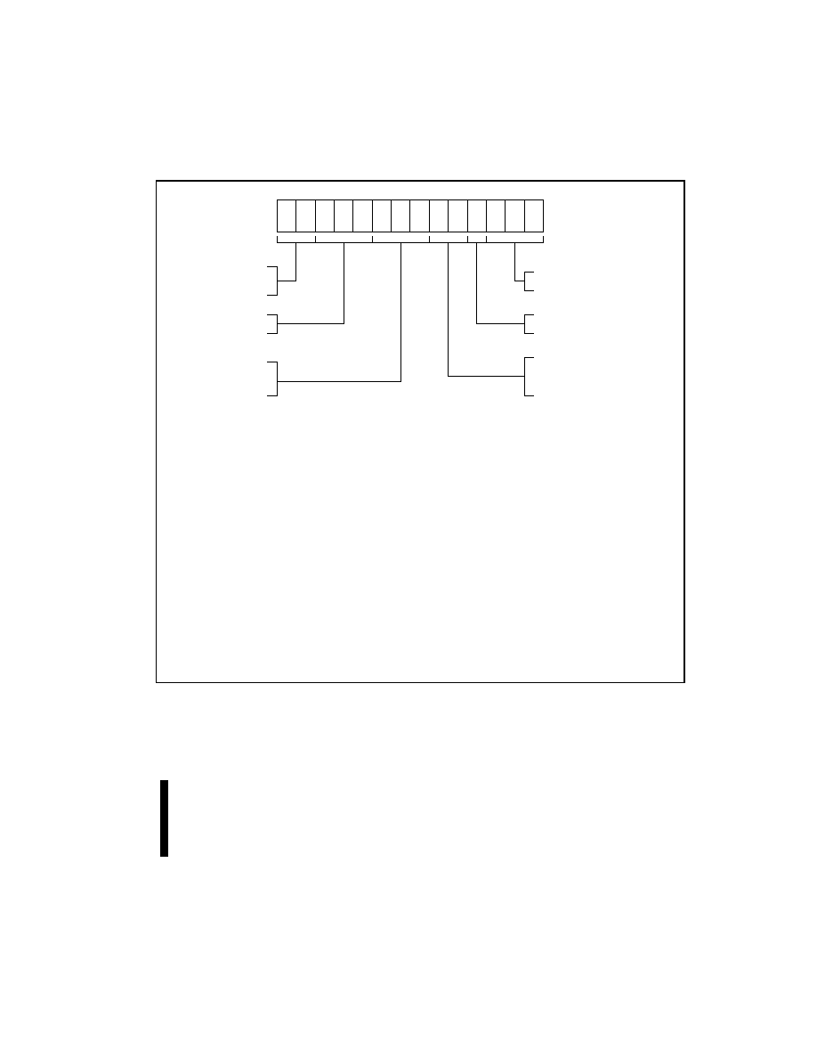
E
SMART 3 ADVANCED BOOT BLOCK≠WORD-WIDE
45
PRELIMINARY
APPENDIX A
ORDERING INFORMATION
T E 2 8 F 1 6 0 B 3 T 1 2 0
Package
TE = 48-Lead TSOP
GT = 48-Ball µBGA* CSP
Product line designator
for all Intel Flash products
Access Speed (ns)
(120, 150)
Product Family
B3 = Smart 3 Advanced Boot Block
V
CC
= 2.7V - 3.6V
V
PP
= 2.7V - 3.6V or 11.4V - 12.6V
Device Density
160 = x16 (16 Mbit)
800 = x16 (8 Mbit)
400 = x 16 (4 Mbit)
T = Top Blocking
B = Bottom Blocking
VALID COMBINATIONS
48-Lead TSOP
48-Ball
µ
BGA* CSP
Extended
16M
TE28F160B3T120
GT28F160B3T120
TE28F160B3B120
GT28F160B3B120
TE28F160B3T150
GT28F160B3T150
TE28F160B3B150
GT28F160B3B150
Extended
8M
TE28F800B3T120
GT28F800B3T120
TE28F800B3B120
GT28F800B3B120
TE28F800B3T150
GT28F800B3T150
TE28F800B3B150
GT28F800B3B150
Extended
4M
TE28F400B3T120
GT28F400B3T120
TE28F400B3B120
GT28F400B3B120
TE28F400B3T150
GT28F400B3T150
TE28F400B3B150
GT28F400B3B150

SMART 3 ADVANCED BOOT BLOCK≠WORD-WIDE
E
46
PRELIMINARY
APPENDIX B
WRITE STATE MACHINE CURRENT/NEXT STATES
Command Input (and Next State)
Current
State
SR.7
Data
When
Read
Read
Array
(FFH)
Program
Setup
(40/10H)
Erase
Setup
(20H)
Erase
Confirm
(D0H)
Program /
Erase
Susp.
(B0H)
Program /
Erase
Resume
(D0)
Read
Status
(70H)
Clear
Status
(50H)
Read ID
(90H)
Read Array
"1"
Array
Read
Array
Program
Setup
Erase
Setup
Read Array
Read
Status
Read
Array
Read
Identifier
Program
Setup
"1"
Status
Pgm.
1
Program (Command input = Data to be programmed)
Program
(Not Comp.)
"0"
Status
Program
Pgm Susp.
to Status
Program
Program
(Complete)
"1"
Status
Read
Array
Program
Setup
Erase
Setup
Read Array
Read
Status
Read
Array
Read
Identifier
Program
Suspend to
Status
"1"
Status
Prog.
Susp. to
Array
Program Suspend
to Array
Program
Program
Susp. to
Array
Program
Prog.
Susp. to
Status
Program Suspend to
Array
Program
Suspend to
Array
"1"
Array
Prog.
Susp. to
Array
Program Suspend
to Array
Program
Program
Susp. to
Array
Program
Prog.
Susp. to
Status
Prog.
Susp. to
Array
Prog.
Susp. to
Array
Erase Setup
"1"
Status
Erase Command Error
Erase
Erase
Cmd. Err.
Erase
Erase Command Error
Erase
Cmd. Error
"1"
Status
Read
Array
Program
Setup
Erase
Setup
Read Array
Read
Status
Read
Array
Read
Identifier
Erase
(Not Comp)
"0"
Status
Erase
Ers. Susp.
to Status
Erase
Erase
(Complete)
"1"
Status
Read
Array
Program
Setup
Erase
Setup
Read Array
Read
Status
Read
Array
Read
Identifier
Erase
Suspend to
Status
"1"
Status
Erase
Susp. to
Array
Program
Setup
Erase
Susp. to
Array
Erase
Erase
Susp. to
Array
Erase
Erase
Susp. to
Status
Erase Suspend
to Array
Erase. Susp.
to Array
"1"
Array
Erase
Susp. to
Array
Program
Setup
Erase
Susp. to
Array
Erase
Erase
Susp. to
Array
Erase
Erase
Susp. to
Status
Erase Suspend
to Array
Read Status
"1"
Status
Read
Array
Program
Setup
Erase
Setup
Read Array
Read
Status
Read
Array
Read
Identifier
Read
Identifier
"1"
ID
Read
Array
Program
Setup
Erase
Setup
Read Array
Read
Status
Read
Array
Read
Identifier
1.
You cannot program "1"s to the flash. Writing FFH following the Program Setup will initiate the internal program algorithm
of the WSM. Although the algorithm will execute, array data is not changed. The WSM returns to read status mode without
reporting any error. Assuming V
PP
> V
PPLK
writing a second FFH while in read status mode will return the flash to read
array mode.

E
SMART 3 ADVANCED BOOT BLOCK≠WORD-WIDE
47
PRELIMINARY
APPENDIX C
ACCESS TIME VS. CAPACITIVE LOAD
(t
AVQV
vs. C
L
)
Access Time vs. Load Capacitance
Derating Curve
115
116
117
118
119
120
121
122
123
124
30
50
70
100
Load Capacitance(pF)
A
cces
s T
i
me(n
s)
Smart 3 Advanced Boot
Block
NOTE:
V
CCQ
= 2.7V
This chart shows a derating curve for device access time with respect to capacitive load. The value in the
DC characteristics section of the specification corresponds to C
L
= 50 pF.
NOTE:
Sampled, but not 100% tested
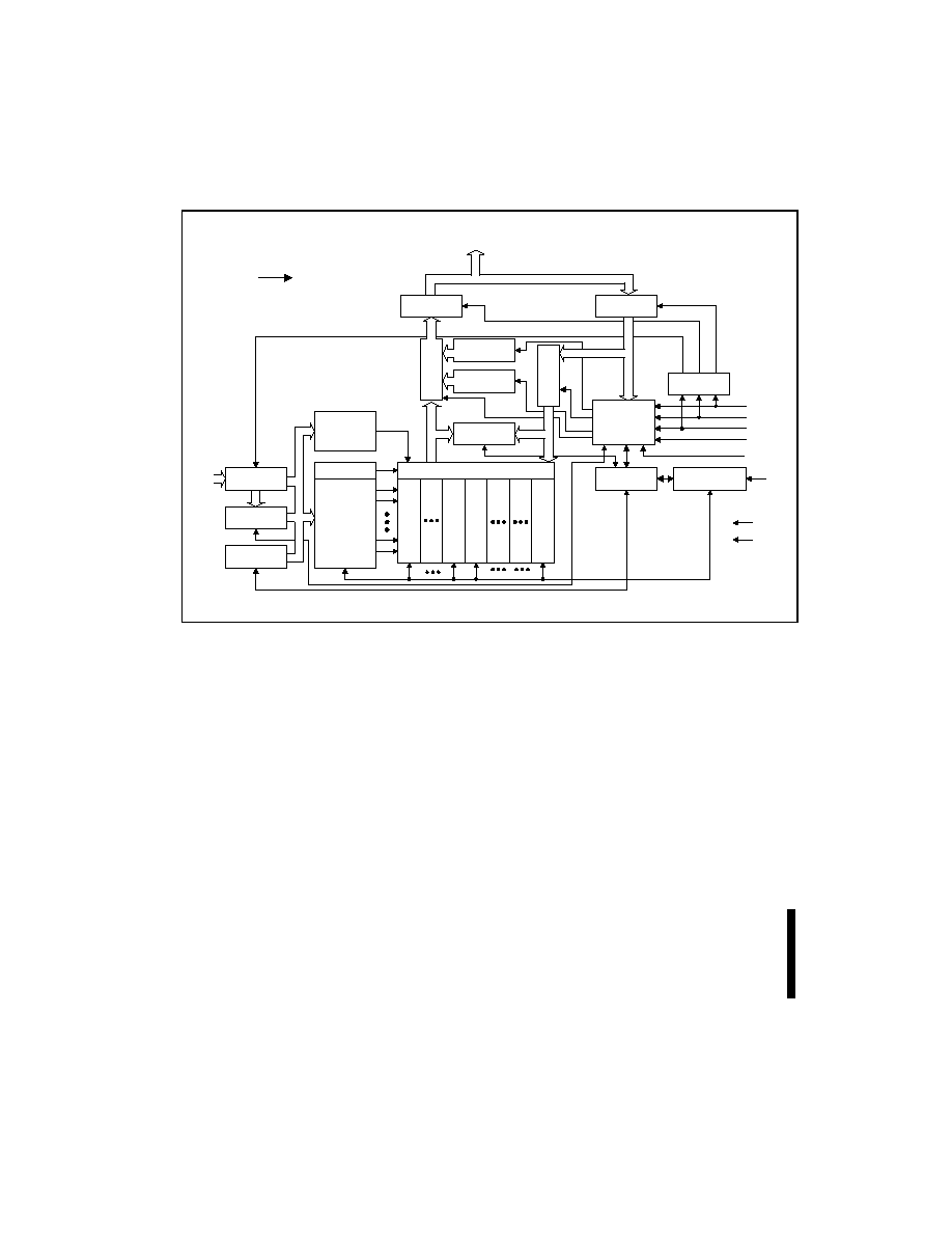
SMART 3 ADVANCED BOOT BLOCK≠WORD-WIDE
E
48
PRELIMINARY
APPENDIX D
ARCHITECTURE BLOCK DIAGRAM
O
utput
Mul
ti
pl
ex
er
4-
KWor
d
P
a
r
ame
ter
B
l
oc
k
3
2
-K
W
o
rd
Ma
i
n
Bl
oc
k
3
2
-K
W
o
rd
Ma
i
n
Bl
oc
k
4-
KWor
d
P
a
r
ame
ter
B
l
oc
k
Y-Gating/Sensing
Write State
Machine
Program/Erase
Voltage Switch
Data
Comparator
Status
Register
Identifier
Register
Data
Regi
s
ter
I/O Logic
Address
Latch
Address
Counter
X-Decoder
Y-Decoder
Power
Reduction
Control
Input Buffer
Output Buffer
GND
V
CC
V
PP
CE#
WE#
OE#
RP#
Command
User
Interface
Input Buffer
A
0
-A
19
DQ
0
-DQ
15
V
CCQ
WP#
0580-20
E
SMART 3 ADVANCED BOOT BLOCK≠WORD-WIDE
49
PRELIMINARY
APPENDIX E
ADDITIONAL INFORMATION
(1,2)
Order Number
Document/Tool
210830
1997 Flash Memory Databook
290605
Smart 3 Advanced Boot Block Byte-Wide 8-Mbit (1024K x8), 16-Mbit
(2056K x 8) Flash Memory Family Datasheet
292172
AP-617 Additional Flash Data Protection Using V
PP
, RP# and WP#
NOTE:
1.
Please call the Intel Literature Center at (800) 548-4725 to request Intel documentation. International customers should
contact their local Intel or distribution sales office.
2.
Visit Intel's World Wide Web home page at http://www.Intel.com for technical documentation and tools.