Copyright© INTEL Corporation, 2002
June 2002
Order Number: 272419-004
Intel386TM SXSA
EMBEDDED MICROPROCESSOR
The Intel386TM SXSA embedded microprocessor is a 5-volt, 32-bit, fully static CPU with a 16-bit external data
bus and a 24-bit external address bus. The Intel386 SXSA CPU brings the vast software library of the Intel386
architecture to embedded systems. It provides the performance benefits of 32-bit programming with the cost
savings associated with 16-bit hardware systems.
The Intel386 SXSA microprocessor is manufactured on Intel's 0.8-micron CHMOS V process. This process
provides high performance and low power consumption for power-sensitive applications. Figure 3 and Figure 4
illustrate the flexibility of low power devices with respect to temperature and frequency relationships.
Static Intel386TM CPU Core
-- Low Power Consumption
-- Operating Power Supply
4.5V to 5.5V - 25 and 33 MHz
4.75V to 5.25V - 40 MHz
-- Operating Frequency
SA-40 = 40 MHz
SA-33 = 33 MHz
SA-25 = 25 MHz
Clock Freeze Mode Allows Clock
Stopping at Any Time
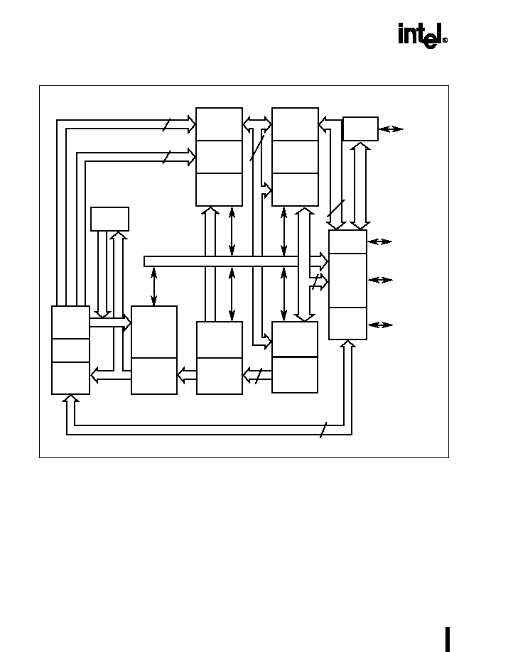
Full 32-bit Internal Architecture
-- 8-, 16-, 32-bit Data Types
-- 8 General Purpose 32-bit Registers
Runs Intel386 Architecture Software in
a Cost-effective, 16-bit Hardware
Environment
-- Runs Same Applications and
Operating Systems as the Intel386
SX and Intel386 DX Processors
-- Object Code Compatible with 8086,
80186, 80286, and Intel386
Processors
TTL-Compatible Inputs
High-performance 16-bit Data Bus
-- Two-clock Bus Cycles
-- Address Pipelining Allows Use of
Slower, Inexpensive Memories
Integrated Memory Management Unit
(MMU)
-- Virtual Memory Support
-- Optional On-chip Paging
-- 4 Levels of Hardware-Enforced
Protection
-- MMU Fully Compatible with 80286
and Intel386 DX Processors
Virtual 8086 Mode Allows Execution of
8086 Software in a Protected and Paged
System
Large Uniform Address Space
-- 16 Megabyte Physical
-- 64 Terabyte Virtual
-- 4 Gigabyte Maximum Segment Size
Numerics Support Intel387TM SX and
Intel387TM SL Math Coprocessors
On-chip Debugging Support Including
Breakpoint Registers
Complete System Development
Support
High Speed CHMOS Technology
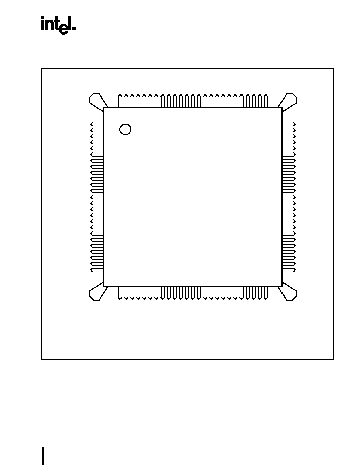
100-Pin Plastic Quad Flatpack Package
Information in this document is provided solely to enable use of Intel products. Intel assumes no liability
whatsoever, including infringe-ment of any patent or copyright, for sale and use of Intel products except as
provided in Intel's Terms and Conditions of Sale for such products. Information contained herein supersedes
previously published specifications on these devices from Intel.

Intel386TM SXSA EMBEDDED MICROPROCESSOR
5
2.0
PIN DESCRIPTIONS
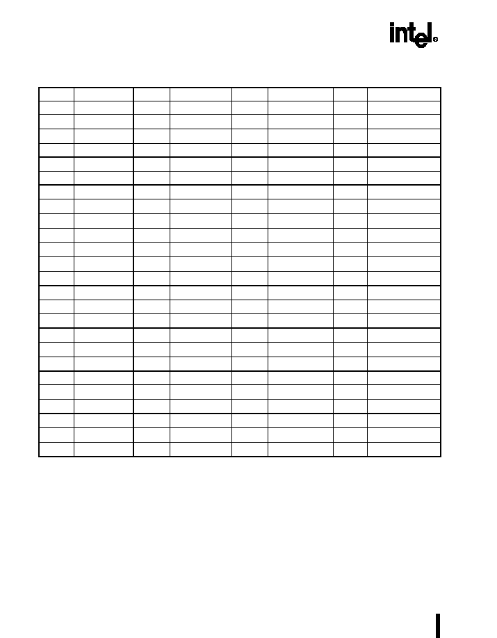
Table 2 lists the Intel386 SXSA microprocessor pin descriptions. The following definitions are used in the pin
descriptions:
#
The named signal is active low.
I
Input signal.
O
Output signal.
I/O Input and output signal.
P
Power pin.
G
Ground pin.
Table 2. Pin Descriptions
Symbol
Type
Pin
Name and Function
A23:1
O
80≠79, 76≠72,
70, 66≠64
62≠58, 56≠51,
18
Address Bus outputs physical memory or port I/O addresses.
ADS#
O
16
Address Status indicates that the processor is driving a valid
bus-cycle definition and address onto its pins (W/R#, D/C#,
M/IO#, BHE#, BLE#, and A23:1).
BHE# O
19
Byte High Enable indicates that the processor is transferring
a high data byte.
BLE#
O
17
Byte Low Enable indicates that the processor is transferring
a low data byte.
BUSY#
I
34
Busy indicates that the math coprocessor is busy.
CLK2
I
15
CLK2 provides the fundamental timing for the device.
D/C#
O
24
Data/Control indicates whether the current bus cycle is a
data cycle (memory or I/O) or a control cycle (interrupt
acknowledge, halt, or code fetch). When D/C# is high, the bus
cycle is a data cycle; when D/C# is low, the bus cycle is a con-
trol cycle.
D15:0
I/O
81≠83, 86≠90,
92≠96, 99≠100,
1
Data Bus inputs data during memory read, I/O read, and
interrupt acknowledge cycles and outputs data during mem-
ory and I/O write cycles.
ERROR#
I
36
Error indicates that the math coprocessor has an error condi-
tion.
FLT#
I
28
Float forces all bidirectional and output signals, including
HLDA, to a high-impedance state.
HLDA
O
3
Bus Hold Acknowledge indicates that the CPU has surren-
dered control of its local bus to another bus master.
HOLD
I
4
Bus Hold Request allows another bus master to request con-
trol of the local bus.
INTR
I
40
Interrupt Request is a maskable input that causes the CPU
to suspend execution of the current program and then exe-
cute an interrupt acknowledge cycle.