 | –≠–ª–µ–∫—Ç—Ä–æ–Ω–Ω—ã–π –∫–æ–º–ø–æ–Ω–µ–Ω—Ç: LXT16642 | –°–∫–∞—á–∞—Ç—å:  PDF PDF  ZIP ZIP |
product brief
Product Description
The Intel
Æ
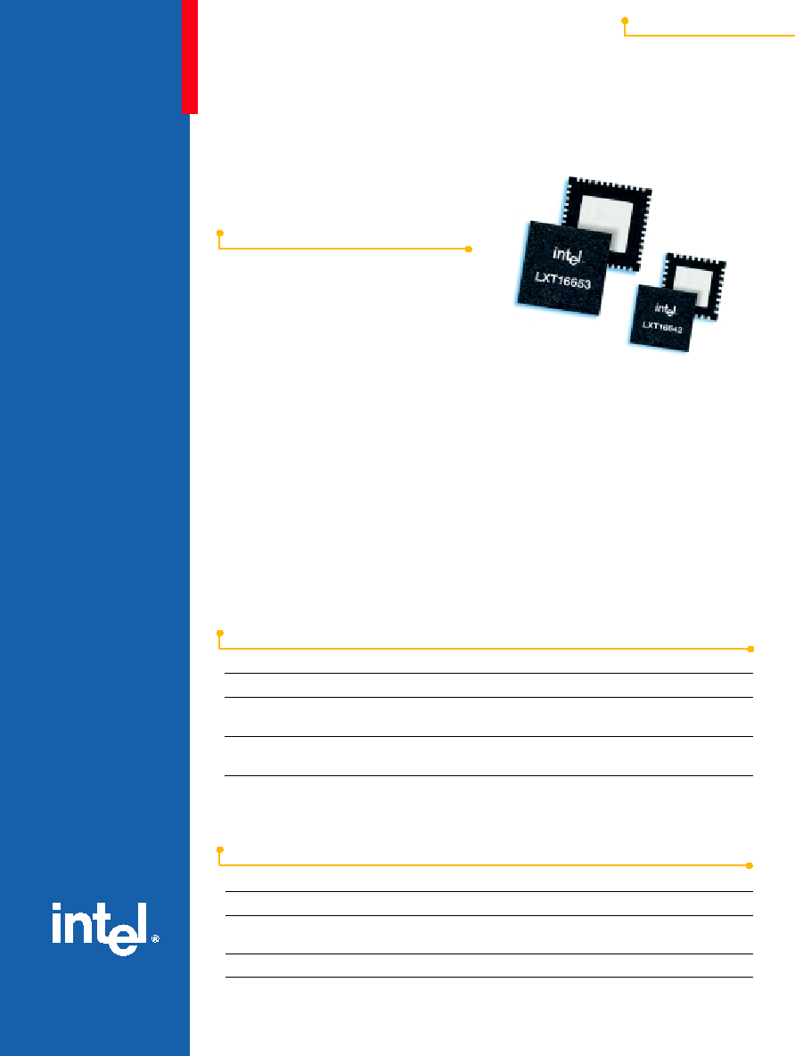
L XT16642 and the Intel
Æ
L XT16653
form a high-performance Serializer/Deserializer
(SerDes) chipset for use in DWDM applications,
SDH STM 16/4, and SONET OC-48/12 Optical
telecommunications systems, and Backplane
applications. The chipset meets the ITU-T and
Telcordia recommendations.
The Intel
Æ
L XT16642/53 chipset is manufac-
tured in a well-proven silicon bipolar technology
that offers the performance, stability, and
reliability customers require for optical com-
munication systems.
The devices are operated from a single power
supply from +2.9V to 3.6V. Power dissipation is
typically 370mW for the L XT16642 and 450mW
for the L XT16653.
The L XT16642 is a high-performance
integrated multi-bit rate Clock and Data
Recovery device (CDR) with 1:4 Demultiplexer
(DeMUX), digital phase detector, out of lock
monitor, Phase Locked Loop (PLL) control
circuit, and Limiting Amplifier (LIA). The system
interface is 4-bit LVDS.
The LXT16653 is a high-performance
integrated multi-bit rate transmitter featuring
a 4:1 Multiplexer (MUX) with integrated clock
generation and PLL circuits. The fully integrated
on-chip PLLs eliminate critical clock and data
timing relations and feature the unique dynamic
phase alignment between ASIC and MUX. The
continuous handling of "round trip delay vari-
ations" by the source synchronous clocking
ensures easy external optimization of jitter.
The system interface is 4-bit LVDS.
s
Easy board design and integration
s
High integration
s
Aggregation point between OC-48 and
OC-192
s
Increased performance
s
Small physical form factor (5mm x 5mm)
s
Reduced board space
Features
Benefits
LXT16642 DeMUX
s
Single power supply: +2.9V to +3.6V
s
Power dissipation: 370mW
s
Interfaces to IXF6192
s
4x L XT16642 interfaces to IXF6192
s
Typically 2x 1.8mVpp @ PRBS 2
23
-1,
BER <10
-12
s
32-pin QFN
s
Easy board design and integration
s
High integration
s
Aggregation point between OC-48 and
OC-192
s
Infinite phase margin tolerance
s
Small physical form factor (7mm x 7mm)
s
Reduced board space
Features
Benefits
LXT16653 MUX
s
Single power supply: +2.9V to +3.6V
s
Power dissipation: 450mW
s
Interfaces to IXF6192
s
4x L XT16653 interfaces to IXF6192
s
Dynamic Phase Alignment based on PLL
s
48-pin QFN
Intel
Æ
LXT16642/LXT16653
Serializer/Deserializer Chipset

Key Features
s
Low-power, small physical form, and high integration
make the chipset ideal for Module and Backplane
applications
s
Easy external optimization of jitter is enabled by a
Dynamic Phase Alignment based on PLL
s
External reference clock facilitates fast acquisition
Key Applications
s
SDH STM 16/4
s
SONET OC-48/12
s
Backplane
s
Aggregation points between OC-48 and OC-192
s
DWDM low-power/low-form factor applications
Application Overview
Intel provides reliable high-performance receivers and
transmitters for optical line cards.
Receiver Line Card
An optical reception system receives an optical signal
and converts it into an electrical signal. The optical
receiver, which can be a PIN diode or an Avalanche
Photo Detector (APD), converts the optical input to a
small electrical current. A Transimpedance Amplifier
(TIA), also known as a post-amplifier, then converts the
current to an electrical voltage. The TIA signal, which
varies from a few mV up to 50mVpp or more, can be
passed to an AGC amplifier or a LIA. This produces a
signal of sufficient amplitude/power to drive the next
building block (see Figure 1).
A CDR converts the analog input signal to a digital bit
stream with an associated clock, and the serial high-
speed data stream is finally converted to a parallel signal
at lower speed. This signal then interfaces to the digital
processing system.
The key function block in the CDR is the PLL, which
locks onto the incoming data stream. The phase detector
is equipped with a discriminator that evaluates the incom-
ing data signal in the middle of the bit period (the "eye")
and determines whether a 1 or a 0 is received.
A separate Lock Detector determines whether the
incoming data rate deviates too much from a given fre-
quency. If data input is absent or deviates too much, the
external reference clock ensures that the VCO remains in
a selectable ±500 to ±2,000ppm capture range.
Phase noise and amplitude noise, also known as jitter,
can cause incorrect determination of data bits (bit errors)
in the input signal. When a valid input signal is applied
both differential data and clock outputs are provided.
The DeMUX transforms the serial data signals into four
parallel data signals at a corresponding lower data rate.
If, for example, a 2.488Gbps signal (OC-48/STM 16) is
fed into a 1:4 DeMUX, it will produce four parallel data
outputs at 622.08Mbps.
Clock output from the CDR is used to clock the data
on the parallel interface into the next device. The Intel
LXT16642 has a DeMUX merged together with a CDR
and is fully compliant with the Optical Interface Forum's
SFI recommendation on common electrical interface
between framers and SerDes.
CLK
CLK
O/E
LDD
MUX
ASIC
Figure 2. Typical transmitter line card
CLK
CLK
O/E
TIA
LIA/AGC
CDR
DeMUX
ASIC
Figure 1. Typical receiver line card

Intel Advantage
Intel is a leading supplier of communications building blocks, adding value at many levels of integration. Through continuous
innovations and advancements in Ethernet connectivity and processing in the network, Intel is delivering, along with its
customers and developer community, a wide choice of solutions that enable faster time-to-market, longer time-in-market,
and increased revenue opportunity.
Transmitter Line Card
In the optical transmission system, the parallel signal
from the processing system is converted to a serial signal
of the bit rate of the optical link. The serial signal is
amplified before it is fed to the laser, which converts the
signal to an electrical signal. The quality of the transmit-
ted optical signal (and so the maximum transmission
distance) is highly dependent on the jitter of the serial
bit stream. The jitter is the phase noise most commonly
caused by the uncertainty or variations in the bit periods.
To resolve this, Intel has directed significant effort in the
system and component design at maintaining precise,
constant duration of the bit periods in the outgoing
data stream (see Figure 2).
The MUX has the opposite functions of the DeMUX.
For example, the MUX might convert a 4-bit parallel signal
into one serial bit stream at a corresponding higher data
rate. When four parallel inputs at 622.08Mbps are fed
into a 4:1 MUX, the output data rate will be 2.488Gbps
for OC-48/STM 16.
The clock interconnections between the MUX and the
data source (such as the framer) can be complex in
high-speed applications. In high-speed clock operation
for MUXs, the input sampling clock must be in the phase
to ensure correct loading of the data into the MUX so
that input data can be sampled correctly. In addition, the
internal high-speed clock used for shifting data to the
laser must be as clean as possible to minimize the jitter
in the output signal. Two PLLs are implemented in each
MUX to accommodate these critical requirements.
System Application Layout
Item
Description
Order Number
Support Collateral/Tools
Application Brief
s
Intel
Æ
IXD66014 10Gbps Line Card Solution for FEC
Enabled SONET/SDH Optical Networking Applications
Utilizing Intel
Æ
IXF32003, GD16588/GD16589**,
LXT16642/LXT16653, and GD16590** products in the
Intel
Æ
IXD66014 Line Card Reference Design
250219
Intel
Æ
IXF6192
Intel
Æ
LXT16642
DeMUX
Intel
Æ
LXT16653
MUX
REFCLK
RXDATA
RXCLK
TXDATA
TXCLK
2.5Gbps
4
4
2.5Gbps
TXCLK SRC

Order Number: 250029-001 Printed in USA/1101/2K/ASI/DC
Copyright © 2001 Intel Corporation
For more information, visit the Intel Web site at:
developer.intel.com
UNITED STATES AND CANADA
Intel Corporation
Robert Noyce Building
2200 Mission College Blvd.
P.O. Box 58119
Santa Clara, CA 95052-8119
USA
EUROPE
Intel Corporation (UK) Ltd.
Pipers Way
Swindon
Wiltshire SN3 1RJ
UK
ASIA-PACIFIC
Intel Semiconductor Ltd.
32/F Two Pacific Place
88 Queensway, Central
Hong Kong, SAR
JAPAN
Intel Japan (Tsukuba HQ)
5-6
Tokodai Tsukuba-shi
300-2635 Ibaraki-ken
Japan
SOUTH AMERICA
Intel Semicondutores do Brasil LTDA
Av. Dr. Chucri Zaidan, 940-10∞ andar
04583-904 S„o Paulo, SP
Brazil
Information in this document is provided in connection with Intel products. No license, express or implied, by estoppel or otherwise, to any intellectual property rights is
granted by this document. Except as provided in Intel's Terms and Conditions of Sale for such products, Intel assumes no liability whatsoever, and Intel disclaims any
express or implied warranty, relating to sale and/or use of Intel products including liability or warranties relating to fitness for a particular purpose, merchantability, or
infringement of any patent, copyright, or other intellectual property right. Intel products are not intended for use in medical, life-saving or life-sustaining applications.
Intel may make changes to specifications and product descriptions at any time, without notice.
Designers must not rely on the absence or characteristics of any features or instructions marked "reserved" or "undefined." Intel reserves these for future definition and
shall have no responsibility whatsoever for conflicts or incompatibilities arising from future changes to them.
Intel is a trademark or registered trademark of Intel Corporation or its subsidiaries in the United States and other countries.
*Other names and brands may be claimed as the property of others. **"GD" indicates an Intel part that retains the branding of Intel's former Giga subsidiary.
Intel Access
Developer Web Site
http://developer.intel.com
Networking Components Home Page
http://developer.intel.com/design/network
Intel Literature Center
http://developer.intel.com/design/litcentr
(800) 548-4725 7 a.m. to 7 p.m. CST (U.S. and Canada)
International locations please contact your local sales office.
General Information Hotline
(800) 628-8686 or (916) 356-3104 5 a.m. to 5 p.m. PST