LXT336
Quad T1/E1 Receiver
Datasheet
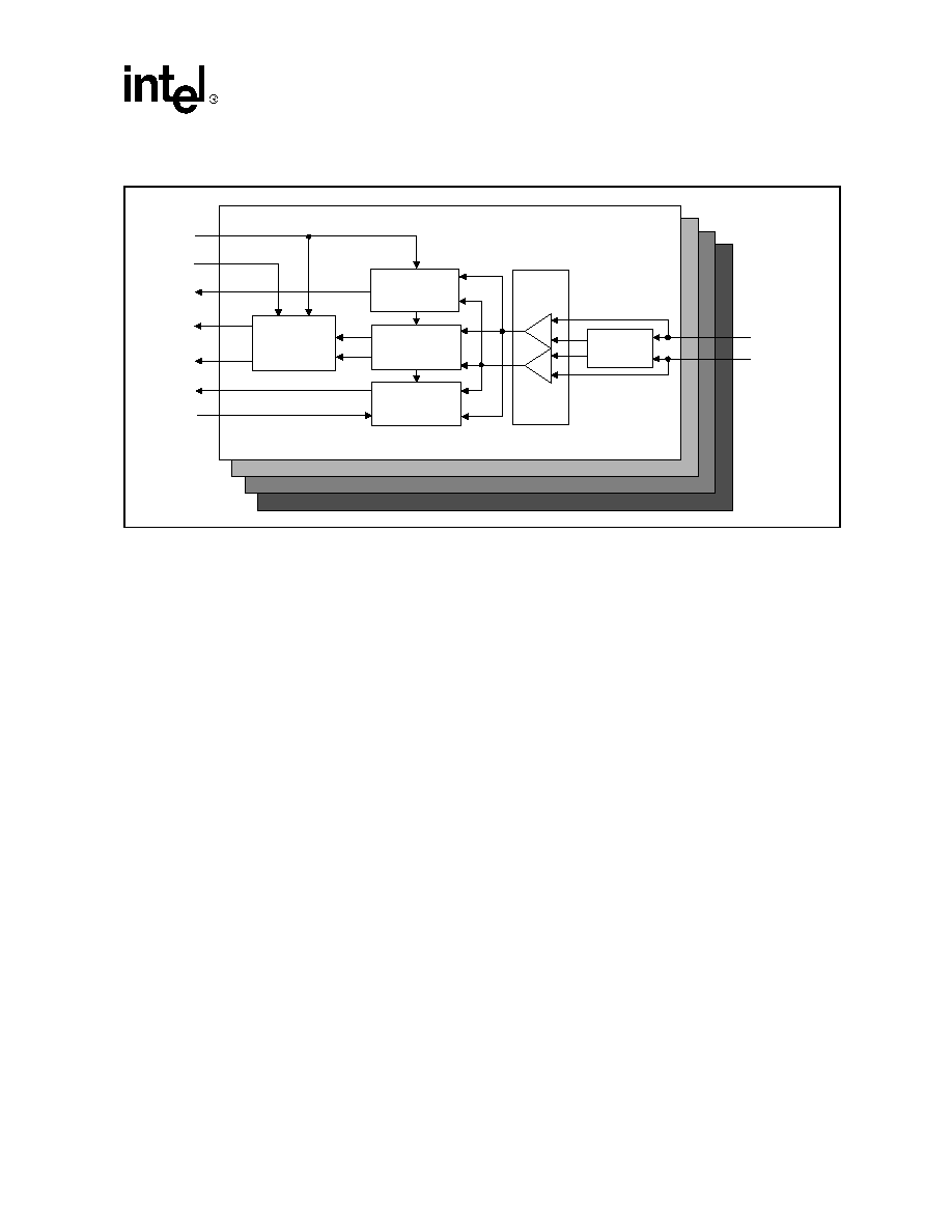
The LXT336 quad receiver is a fully-integrated, quadruple-PCM receiver for both T1 (1.544
Mbps) and E1 (2.048 Mbps) applications. It incorporates four independent receivers in a single
64-pin QFP package.
The LXT336 features a differential receiver architecture with high noise interference margin. It
uses peak detection with a variable threshold for reliable recovery of data as low as 500 mV and
up to 12 dB of cable attenuation.
The fully digital clock recovery system uses a low frequency master clock of 2.048 MHz or
1.544 MHz as its reference. In addition, each LXT336 receiver incorporates a Loss of Signal
(LOS) detection circuit. The LOS detector is compliant with both ITU-T G.775 and ANSI
T1.231 standards.
The LXT336 ports can be independently configured for either unipolar or bipolar output modes.
HDB3 and AMI decoding mechanisms are available in unipolar mode.
Applications
Product Features
s
Test Equipment
s
DSX-1 and E1 Line Monitoring
s
High density T1/E1 line cards
s
Fully integrated quad, receiver for E1 2.048
Mbps or T1 1.544 Mbps operation
s
Single rail supply voltage of 5 V (typical)
s
Low power consumption: 250 mW for E1;
200 mW for T1 (typical)
s
High-performance receivers recover data
with up to 12 dB cable attenuation
s
On-chip clock recovery function complies
with ITU G.823 and Bellcore GR-499-
CORE
s
Low frequency 1.544 or 2.048 MHz
reference clock
s
Programmable unipolar and bipolar PCM
interface
s
On-chip AMI and HDB3 decoders
s
Loss of Signal processors conform to ITU
G.775 and ANSI T1.231 recommendations
s
Small-footprint 64-pin QFP
s
Optional RZ Data recovery mode
As of January 15, 2001, this document replaces the Level One document
Order Number: 249046-001
LXT336 -- Quad T1/E1 Receiver.
January 2001

Datasheet
Information in this document is provided in connection with Intel
Æ
products. No license, express or implied, by estoppel or otherwise, to any intellectual
property rights is granted by this document. Except as provided in Intel's Terms and Conditions of Sale for such products, Intel assumes no liability
whatsoever, and Intel disclaims any express or implied warranty, relating to sale and/or use of Intel products including liability or warranties relating to
fitness for a particular purpose, merchantability, or infringement of any patent, copyright or other intellectual property right. Intel products are not
intended for use in medical, life saving, or life sustaining applications.
Intel may make changes to specifications and product descriptions at any time, without notice.
Designers must not rely on the absence or characteristics of any features or instructions marked "reserved" or "undefined." Intel reserves these for
future definition and shall have no responsibility whatsoever for conflicts or incompatibilities arising from future changes to them.
The LXT336 may contain design defects or errors known as errata which may cause the product to deviate from published specifications. Current
characterized errata are available on request.
Contact your local Intel sales office or your distributor to obtain the latest specifications and before placing your product order.
Copies of documents which have an ordering number and are referenced in this document, or other Intel literature may be obtained by calling 1-800-
548-4725 or by visiting Intel's website at http://www.intel.com.
Copyright © Intel Corporation, 2001
*Third-party brands and names are the property of their respective owners.

Datasheet
3
Quad T1/E1 Receiver -- LXT336
Contents
1.0
Pin Assignments & Signal Descriptions\
......................................................... 6
2.0
Functional Description
........................................................................................... 10
2.1
Receiver Description ........................................................................................... 10
2.1.1
Loss Of Signal Detector ......................................................................... 10
2.1.1.1 E1 LOS Detection...................................................................... 10
2.1.1.2 T1 LOS Detection ...................................................................... 11
2.1.1.3 Data Recovery Mode LOS Detection ........................................ 11
2.1.1.4 In-Service Code Violation Monitoring ........................................ 11
3.0
Application Information
.........................................................................................12
3.1
Monitoring Applications ....................................................................................... 12
3.1.1
Receive Line Interface Applications ....................................................... 13
4.0
Test Specifications
.................................................................................................. 16
5.0
Mechanical Specifications
.................................................................................... 22
Figures
1
LXT336 Block Diagram ......................................................................................... 5
2
LXT336 Pin Assignments and Package Markings ................................................ 6
3
Typical Monitoring Application............................................................................. 13
4
Typical Receive Line Interface Application.......................................................... 14
5
LXT336 Receive Timing Diagram ....................................................................... 19
6
E1 Jitter Tolerance--G.823................................................................................. 20
7
T1 Jitter Tolerance--GR-499-CORE Category II ................................................ 21
8
Package Specifications ....................................................................................... 22
Tables
1
LXT336 Pin Descriptions....................................................................................... 7
2
Transformer Specifications..................................................................................15
3
Absolute Maximum Ratings................................................................................. 16
4
Recommended Operating Conditions ................................................................. 16
5
DC Characteristics (Over Recommended Range) .............................................. 16
6
E1 Receive Characteristics (Over Recommended Range) ................................. 17
7
T1 Receive Characteristics (Over Recommended Range) ................................. 18
8
Timing Characteristics (Over Recommended Range)......................................... 19
9
Relevant Recommendations ............................................................................... 21