
LXT6051
STM-1/0 SDH Overhead Terminator
Datasheet
The LXT6051 Overhead Terminator implements the Regenerator Section Termination,
Multiplexer Section Termination and Higher Order Path Termination in STM-0 (51Mb/s) and
STM-1 (155Mb/s) multiplexers. It provides micro-controller access for performance monitoring,
alarm detection and configuration for transmit and receive paths. When used with the
LXT6251A (21E1 Mapper), a complete solution for a 21 E1 or a 63 E1 Multiplexer is created.
The LXT6051 is compliant with the latest releases of ITU-T G.703 and G.707. It provides all the
alarm and control features to easily implement the multiplexer described in ITU-T G.783.
Product Features
n
SDH Terminal Mux/ADM for microwave
radio
n
ADM fiber ring Mux
n
Digital Loop Carrier (NGDLC) Systems
n
Digital Cross-Connect System
n
Performs Regenerator Section, Multiplexer
Section, and Higher Order Path Overhead
Processing for STM-1 and STM-0 signals.
n
Byte parallel interface for STM-1 or STM-
0, with byte alignment performed
internally. Serial NRZ or B3ZS interface
option for STM-0.
n
Demultiplexes STM-0/STM-1 signals to
Telecom Bus output with optional pointer
processor re-timing.
n
Multiplexes Telecom Bus data into STM-0
or STM-1 signals with pointer processing.
n
Compatible with 1+1 protected ITU
architecture.
n
Records all RSOH, MSOH, and HPOH
alarms. One second counters for B1, B2,
B3, M1 REI and G1 REI.
n
Full J0/J1 trace identifier processing.
n
Serial access to STM-1 user-defined,
media-dependent and national bytes.
n
Dedicated pins for serial access or pass-
through feature for E1, E2, F1, F2, F3, D1-
D3 & D4-D12 bytes.
n
Low power CMOS technology with 3.3V
core and 5V I/O in PQFP-208 package.
n
IEEE 1149.1 Boundary Scan (JTAG)
support.
As of January 15, 2001, this document replaces the Level One document
Order Number: 249302-001
LXT6051 STM-1/0 SDH Overhead Terminator Datasheet.
January 2001

Datasheet
Information in this document is provided in connection with Intel
�
products. No license, express or implied, by estoppel or otherwise, to any intellectual
property rights is granted by this document. Except as provided in Intel's Terms and Conditions of Sale for such products, Intel assumes no liability
whatsoever, and Intel disclaims any express or implied warranty, relating to sale and/or use of Intel products including liability or warranties relating to
fitness for a particular purpose, merchantability, or infringement of any patent, copyright or other intellectual property right. Intel products are not
intended for use in medical, life saving, or life sustaining applications.
Intel may make changes to specifications and product descriptions at any time, without notice.
Designers must not rely on the absence or characteristics of any features or instructions marked "reserved" or "undefined." Intel reserves these for
future definition and shall have no responsibility whatsoever for conflicts or incompatibilities arising from future changes to them.
The LXT6051 may contain design defects or errors known as errata which may cause the product to deviate from published specifications. Current
characterized errata are available on request.
Contact your local Intel sales office or your distributor to obtain the latest specifications and before placing your product order.
Copies of documents which have an ordering number and are referenced in this document, or other Intel literature may be obtained by calling 1-800-
548-4725 or by visiting Intel's website at http://www.intel.com.
Copyright � Intel Corporation, 2001
*Third-party brands and names are the property of their respective owners.

Datasheet
3
STM-1/0 SDH Overhead Terminator -- LXT6051
Contents
1.0
Block Diagram
........................................................................................................... 11
2.0
Pin Assignments And Signal Description
...................................................... 12
3.0
Functional Description
........................................................................................... 22
3.1
Transmit Data Flow ............................................................................................. 22
3.2
Receive Data Flow .............................................................................................. 23
3.2.1
Reference Clocks ................................................................................... 26
3.3
Modes of Operation............................................................................................. 26
3.3.1
Chip Configuration..................................................................................26
3.3.2
Repeater Mode Configuration ................................................................ 26
3.3.3
Terminal Mode Configuration (No Protection) ........................................ 27
3.3.3.1 Receive Side Telecom Bus Timing Source ...............................28
3.3.3.2 Transmit Side Telecom Bus Timing Source .............................. 28
3.3.4
Add and Drop Configuration ................................................................... 29
3.3.4.1 Receive Side Telecom Bus Timing Source ...............................29
3.3.4.2 Transmit Side Telecom Bus Timing Source .............................. 29
3.3.4.3 Updating the Transmit AU Pointer Justification Event
Counters .................................................................................... 30
3.3.5
Terminal Protection Mode ...................................................................... 31
3.3.5.1 Receive Side Telecom Bus Timing Source ...............................31
3.3.5.2 Transmit Side Telecom Bus Timing Source .............................. 31
3.3.6
Receiver Default Operation .................................................................... 31
3.3.6.1 Serial Interface .......................................................................... 31
3.3.6.2 Parallel Interface ....................................................................... 32
3.3.6.3 Clock Distribution and Reference .............................................. 34
3.3.6.4 Framer ....................................................................................... 34
3.3.6.5 Regenerator Section Receiver ..................................................36
3.3.6.6 Multiplexer Section Receiver ..................................................... 38
3.3.6.7 Multiplexer Section Protection (MSP) Block .............................. 40
3.3.6.8 Pointer Recovery ....................................................................... 40
3.3.6.9 Higher Order Path Receiver ...................................................... 41
3.3.6.10Re-Timing Function ................................................................... 43
3.3.7
Transmitter Default Operation ................................................................ 44
3.3.7.1 Higher Order Path Transmitter ..................................................44
3.3.7.2 Transmit Pointer Processing Function ...................................... 46
3.3.7.3 Transmit Multiplex Section Protection (MSP Block) ..................47
3.3.7.4 Multiplexer Section Transmitter ................................................. 47
3.3.7.5 Regenerator Section Transmitter .............................................. 49
3.3.7.6 Parallel Interface ....................................................................... 52
3.3.7.7 Serial Interface .......................................................................... 52
3.3.7.8 Clock Distribution and Reference .............................................. 52
4.0
Functional Timing
.................................................................................................... 55
4.1
Transmit Frame Parallel Timing .......................................................................... 55
4.2
Transmit Frame Serial Timing ............................................................................. 56
4.3
Receive Re-timing Functional Timing.................................................................. 57
4.4
Telecom Bus Interface ........................................................................................ 57
4.4.1
Multiplexer Telecom Bus Terminal Mode ............................................... 57

LXT6051 -- STM-1/0 SDH Overhead Terminator
4
Datasheet
4.4.2
Multiplexer Telecom Bus ADM Mode ..................................................... 58
4.4.3
Demultiplexer Telecom Bus (Terminal or ADM) Mode........................... 59
4.4.4
Protection Bus Interface Timing ............................................................. 62
4.4.5
Transmitter "Master" in 1+1 Protection Configuration ............................ 63
4.4.6
Transmitter "Slave" in 1+1 Protection Configuration .............................. 63
4.4.7
Receive"Master" in 1+1 Protection Configuration .................................. 63
4.4.8
Receive "Slave" Configuration (1+1 Protection)..................................... 64
4.4.9
OverHead Byte Access Timing .............................................................. 66
4.5
F2 and F3 Digital Channel Functional Timing ..................................................... 66
4.5.1
Transmit side access ............................................................................. 66
4.5.2
Receive Side Access ............................................................................. 67
4.5.3
E1, E2 and F1 Orderwire Channel Functional Timing............................ 67
4.5.3.1 Transmit Timing......................................................................... 67
4.5.3.2 Receive timing........................................................................... 68
4.5.4
HPOH Bytes Serial Access Functional Timing....................................... 68
4.5.4.1 Transmit serial HPOH Timing.................................................... 68
4.5.4.2 Receive Serial HPOH Timing .................................................... 69
4.5.5
SOH Overhead Access Functional Timing............................................. 70
4.5.5.1 Transmit Side SOH Serial Timing ............................................. 70
4.5.5.2 Receive Side SOH Serial Timing .............................................. 71
4.5.6
D1 to D3 Data Communication Channel Functional Timing................... 72
4.5.6.1 Transmit Side Access................................................................ 72
4.5.6.2 Receive Side Access................................................................. 72
4.5.7
D4 to D12 Data Communication Channel .............................................. 73
4.5.7.1 Transmit Side Access................................................................ 73
4.5.7.2 Receive Side Access................................................................. 73
4.6
BIP Receive Functional Timing ........................................................................... 74
5.0
Test Specifications
.................................................................................................. 75
6.0
Microprocessor Interface & Register Description
...................................... 91
6.1
Microcontroller Interface...................................................................................... 91
6.1.1
Intel interface.......................................................................................... 91
6.1.2
Motorola interface .................................................................................. 91
6.1.3
Interrupt Handling................................................................................... 92
6.1.3.1 Interrupt Sources....................................................................... 92
6.1.3.2 Interrupt Enables ....................................................................... 92
6.1.3.3 Interrupt Clearing....................................................................... 92
6.1.3.4 Status Registers Access ........................................................... 93
6.1.3.5 C2, K3, K2, K1 and S1 Receive Byte Registers Access ........... 93
6.1.4
Counter Reading .................................................................................... 93
6.2
Register Address Map......................................................................................... 93
6.3
Global Registers.................................................................................................. 97
6.3.1
OCR1--Operational Configuration 1 (50H)............................................ 97
6.3.2
OCR2--Operational Configuration 2 (51H)............................................ 98
6.3.3
CHIP_ID--Chip ID Number (52H).......................................................... 99
6.3.4
BUF_ACNTS--Buffer All Counters (54H) .............................................. 99
6.4
Receive Regenerator Section Termination Registers ......................................... 99
6.4.1
R_RSTC1--Receive RST Configuration 1 (40H)................................... 99
6.4.2
R_RSTC2--Receive RST Configuration 2 (47H)................................. 100
6.4.2.1 LOF_LMN--Loss of Frame L, M, & N Configuration

Datasheet
5
STM-1/0 SDH Overhead Terminator -- LXT6051
(41�42H) ................................................................................. 101
6.4.3
OOF_ECNT--Out Of Frame Event Counter (44�43H) ........................ 101
6.4.4
B1_ERRCNT--B1 Error Counter (46�45H) ......................................... 101
6.5
Receive Regenerator and Multiplexer Section Termination Registers.............. 102
6.5.1
J0_RSTR_C--J0 Expected String Control (0EH) ................................ 102
6.5.2
J0_RSTR_D--J0 Expected String Data (0FH)..................................... 102
6.5.3
WINSZ_SB2--Window Size for Setting ExcB2ErrSt (1C�1BH)........... 102
6.5.4
CWIN_SB2--Consecutive Windows for Setting ExcB2ErrSt (1DH) .... 103
6.5.5
E#_EXCWIN--Number of Errs/Win for Excessively Errored Window
(1EH) ....................................................................................................103
6.5.6
WINSZ_C2--Window Size for Clearing ExcB2ErrSt (16�15H)............ 103
6.5.7
CWIN_CB2--Consecutive Windows for Clearing ExcB2ErrSt (17H)...103
6.5.8
E#_NEXCWIN--Number of Errs/Win for Non-Excessively Errored
Window (18H).......................................................................................104
6.5.9
B2_BLKCNT--B2 Block Error Counter (11�10H) ................................ 104
6.5.10 B2_BIPCNT--B2 BIP Error Counter (14�12H) .................................... 104
6.5.11 MR_BLKCNT--MST REI Block Error Counter (0A�09H) .................... 104
6.5.12 MR_BIPCNT--MST REI BIP Error Counter (0D�0BH) ........................ 105
6.5.13 R_K1--Received K1 byte (00H)........................................................... 105
6.5.14 R_K2--Received K2 Byte (01H) .......................................................... 105
6.5.15 R_S1--Received S1 byte (02H)........................................................... 105
6.5.16 R_NU1_8--Received Nu1_8 byte (03H).............................................. 105
6.5.17 R_NU1_9--Received Nu1_9 byte (04H).............................................. 105
6.5.18 R_NU2_8--Received Nu2_8 byte (05H).............................................. 106
6.5.19 R_NU2__9--Received Nu2_9 byte (06H)............................................ 106
6.5.19.1R_NU9_8--Received Nu9_8 byte (07H)................................. 106
6.5.20 R_NU9_9--Received Nu9_9 byte (08H).............................................. 106
6.6
Receive Multiplexer Section Protection Registers............................................. 107
6.6.1
R_MSP_C--Receive MSP Configuration (20H)...................................107
6.6.2
R_MSP_OP--Receive MSP Operational (21H) ...................................107
6.6.3
R_PROTK1--Received K1 byte on Protection Bus from Slave (22H) . 107
6.7
R_PROTK2--Received K2 byte on Protection Bus from Slave (23H) .............. 108
6.8
Receive Multiplexer Section Adaptation Registers............................................ 108
6.8.1
R_MSA_C--Receive MSA Configuration (90H)...................................108
6.8.2
R_AU_NCNT--Receive Negative AU Pointer Justification Event
Counter (92�91H)................................................................................. 108
6.8.2.1 R_AU_PCNT--Receive Positive AU Pointer Justification Event
Counter (94�93H).................................................................... 109
6.9
Receive HighOrder Path Termination Registers ............................................... 109
6.9.1
R_HPT_C1--Receive HPT Configuration 1 Register (80H) ................109
6.9.2
R_HPT_C2--Receive HPT Configuration 2 Register (81H) ................110
6.9.3
J1_RSTR_C--J1 Expected String Control Register (8AH) .................. 111
6.9.4
J1_RSTR_D--J1 Expected String Data Register (8BH) ......................111
6.9.5
EXP_C2--Expected C2 byte Register (82H) ....................................... 111
6.9.6
R_C2--Received C2 byte Register (83H)............................................ 111
6.9.7
R_K3--Received K3 byte Register (84H) ............................................ 111
6.9.8
R_HPT_RDI--Received HPT RDI Bits Register (85H) ........................ 112
6.9.9
B3_ECNT--B3 Error Event Counter (87�86H) .................................... 112
6.9.10 HPTREI_CNT--HPT REI Counter (89�88H) ....................................... 112
6.10
Transmit Regenerator and Multiplexer Section Termination Registers............. 113

LXT6051 -- STM-1/0 SDH Overhead Terminator
6
Datasheet
6.10.1 T_RMST_OP1--Transmit RMST Operational 1 Register (30H) .......... 113
6.10.2 T_RMST_OP2--Transmit RMST Operational 2 Register (1AH).......... 113
6.10.3 T_SC1_SOH--Transmit Source Configuration 1 for SOH bytes
Register (60H) ...................................................................................... 114
6.10.4 T_SC2_SOH--Transmit Source Configuration 2 for SOH bytes
Register (61H) ...................................................................................... 115
6.10.5 T_SC3_SOH--Transmit Source Configuration 3 for SOH Bytes
Register (62H) ...................................................................................... 116
6.10.6 T_SC4_SOH--Transmit Source Configuration 4 for SOH Bytes
Register (63H) ...................................................................................... 116
6.10.7 J0_TSTR_C--J0 Transmit String Control Register (3AH) ................... 117
6.10.8 JO_TSTR_D--J0 Transmit String Data Register (3BH)....................... 118
6.10.9 MP_TNU1_8--Microprocessor Provided Transmit Nu1_8 Byte (31H) 118
6.10.10 MP_TNU1_9--Microprocessor Provided Transmit Nu1_9 Byte
Register (32H) ...................................................................................... 118
6.10.11 MP_TNU2_8--Microprocessor Provided Transmit Nu2_8 Byte (33H) 118
6.10.12 MP_TNU2_9--Microprocessor Provided Transmit Nu2_9 Byte
Register (34H) ...................................................................................... 118
6.10.13 MP_TNU9_8--Microprocessor Provided Transmit Nu9_8 Byte (35H) 118
6.10.14 MP_TNU9_9--Microprocessor Provided Transmit Nu9_9 Byte (36H) 119
6.10.15 MP_TK1--Microprocessor Provided Transmit K1 Byte Register
(37H) .................................................................................................... 119
6.10.16 MP_TK2--Microprocessor Provided Transmit K2 Byte Register
(38H) .................................................................................................... 119
6.10.17 MP_TS1--Microprocessor Provided Transmit S1 Byte Register
(39H) .................................................................................................... 119
6.11
Transmit Multiplexer Section Adaptation Registers .......................................... 119
6.11.1 T_AU_NCNT--Transmit Negative AU Pointer Justification Event
Counter (E3�E2H)................................................................................ 120
6.11.2 T_AU_PCNT--Transmit Positive AU Pointer Justification Event
Counter (E5�E4H)................................................................................ 120
6.12
Transmit HighOrder Path Termination Registers .............................................. 120
6.12.1 T_SC_HPOH--Transmit Source Configuration for HPOH bytes (70H)120
6.12.2 T_HPT_C--Transmit HPT Configuration (71H) ................................... 122
6.12.3 MP_TC2--Microprocessor Provided Transmit C2 Byte (72H) ............. 122
6.12.4 MP_TK3--Microprocessor Provided Transmit K3 Byte (73H) ............. 123
6.12.5 MP_THPTRDI--Microprocessor Provided Transmit HPT RDI bits
(74H) .................................................................................................... 123
6.12.6 J1_TSTR_C--J1 Transmit String Control (75H) .................................. 123
6.12.7 J1_TSTR_D--J1 Transmit String Data (76H) ...................................... 123
6.13
Interrupt Source Registers ................................................................................ 124
6.13.1 IS_RG--Receive Regenerator Section Interrupt Source (A0H)........... 124
6.13.2 IS_RGMUX--Receive Regenerator and Multiplexor Section Interrupt
Source (A1H) ....................................................................................... 124
6.13.3 IS_MUX--Receive Multiplexer Section Interrupt Source (A2H)........... 125
6.13.4 IS_PROT--Receive Protection Section Interrupt Source (A3H) .......... 125
6.13.4.1IS_A_HPT--Receive Adaptation and HPT Interrupt Source
(A4H) ....................................................................................... 125
6.13.5 IS_HPT--Receive HPT Interrupt Source (A5H)................................... 126
6.13.6 IS_RETIME--Receive Retiming Interrupt Source (A6H) ..................... 126
6.13.7 IS_XMT--Transmit Interrupt Source (E0H).......................................... 127

Datasheet
7
STM-1/0 SDH Overhead Terminator -- LXT6051
6.13.8 IS_GLOB--Global Interrupt Source (D1H)........................................... 127
6.14
Interrupt Enable Registers................................................................................. 128
6.14.1 IE_RG--Receive Regenerator Section Interrupt Enable (B0H) ........... 128
6.14.2 IE_RGMUX--Receive Regenerator and Multiplexer Section Interrupt
Enable (B1H)........................................................................................ 128
6.14.3 IE_MUX--Receive Multiplexer Section Interrupt Enable (B2H) ........... 128
6.14.4 IE_PROT--Receive Protection Section Interrupt Enable (B3H) .......... 128
6.14.5 IE_A_HPT--Receive Adaptation and HPT Interrupt Enable (B4H) ..... 128
6.14.6 IE_HPT--Receive HPT Interrupt Enable (B5H) ...................................128
6.14.7 IE_RETIME--Receive Retiming Interrupt Enable (B6H)......................129
6.14.8 IE_XMT--Transmit Interrupt Enable (E1H) ..........................................129
6.15
Status Registers ................................................................................................ 129
6.15.1 S_RG--Receive Regenerator Section Status (C0H). .......................... 129
6.15.2 S_RGMUX--Receive Regenerator and Multiplexer Section Status
(C1H) ....................................................................................................129
6.15.3 S_PROT--Receive Protection Section Status (C3H) .......................... 130
6.15.4 S_A_HPT--Receive Adaptation and HPT Status (C4H)......................130
6.15.5 S_HPT--Receive HPT Status (C5H) ................................................... 131
6.15.6 S_AIS_PROT--Receive AIS & Protection Switch Status (D0H).......... 131
7.0
Testability
.................................................................................................................. 133
7.1
IEEE 1149.1 Boundary Scan............................................................................. 133
7.2
Instruction Register and Definitions...................................................................134
7.3
Boundary Scan Register ................................................................................... 135
7.4
Summary Information ........................................................................................ 135
8.0
Package Information
.............................................................................................143
9.0
Glossary of Terms
................................................................................................. 144
Figures
1
LXT6051 Block Diagram ..................................................................................... 11
2
LXT6051 Pin Assignment.................................................................................... 12
3
LXT6051 Block Diagram ..................................................................................... 24
4
STM-0 Repeater Application .............................................................................. 27
5
STM-1 Terminal Multiplexer ............................................................................... 29
6
STM-1 ADM Configuration With 42 E1 Access ................................................... 30
7
Terminal Protection Mode Data Flow .................................................................. 32
8
LXT6051 Receiver Blocks ................................................................................... 34
9
STM-0 Robust Frame State Machine.................................................................. 35
10
LOF State Machine ............................................................................................. 36
11
Overhead Bytes for the STM-1............................................................................37
12
Transmit Detail Block Diagram ............................................................................44
13
Transmit Frame Reference Timing Parallel Interface.......................................... 55
14
Transmit Frame Reference Timing Serial Interface (STM-0) .............................. 56
15
Receive Re-Timing Function Timing ................................................................... 57
16
STM-0 Telecom Bus Timing................................................................................ 61
17
STM-1 Telecom Bus Timing................................................................................ 62
18
Master MSP Interface Timing............................................................................. 65

LXT6051 -- STM-1/0 SDH Overhead Terminator
8
Datasheet
19
Slave MSP Interface Timing................................................................................ 66
20
Transmit F2 and F3 Orderwire Timing ................................................................ 67
21
Receive F2 and F3 Orderwire Timing ................................................................. 67
22
Transmit Orderwire E1, E2 and F1 Timing.......................................................... 68
23
Receive Orderwire E1, F1 and E2 Timing........................................................... 68
24
Transmit HPOH Serial Bus Timing...................................................................... 69
25
Receive HPOH Serial Bus Timing....................................................................... 70
26
Transmit TSOH Serial Bus Timing ...................................................................... 71
27
Receive RSOH Timing ........................................................................................ 72
28
Transmit D1 to D3 Timing ................................................................................... 72
29
Receive D1 to D3 Timing .................................................................................... 73
30
Transmit D4 to D12 Timing ................................................................................. 73
31
Receive D4 to D12 Timing .................................................................................. 74
32
BIP Functional Timing ......................................................................................... 74
33
Serial Interface Timing ........................................................................................ 76
34
Parallel Interface Timing ..................................................................................... 76
35
Receive Re-Timing Function Timing ................................................................... 77
36
Transmit Frame Parallel Timing .......................................................................... 78
37
Transmit Frame Serial Timing ............................................................................. 79
38
Receive Telecom Bus Timing ............................................................................. 80
39
ADM Mode Transmit Telecom Bus Timing ......................................................... 80
40
Terminal Mode Transmit Telecom Bus Timing ................................................... 81
41
Master Mode MSP Bus Timing .......................................................................... 82
42
Slave Mode MSP Bus Timing ............................................................................. 83
43
Microprocessor Read Timing .............................................................................. 84
44
Microprocessor Write Timing .............................................................................. 85
45
Orderwire E1, F1 & E2, F2 & F3 Timing ............................................................. 86
46
Data Communication Channel Timing ................................................................ 87
47
Serial Overhead Interface Timing ....................................................................... 89
48
BIP Alarm output Timing ..................................................................................... 90
49
Test Access Port ............................................................................................... 133
50
Instruction Register ........................................................................................... 134
51
Boundary Scan Cell .......................................................................................... 136

Datasheet
9
STM-1/0 SDH Overhead Terminator -- LXT6051
Tables
1
Signal Description Nomenclature ........................................................................ 13
2
Signal Description ...............................................................................................13
3
Power, Ground, and No Connects ...................................................................... 21
4
Repeater Clocks.................................................................................................. 27
5
G1x RDI Bit Coding ............................................................................................. 45
6
K2 RDI Bit Coding ...............................................................................................48
7
Operating Mode Vs. Input Clock Source Reference ........................................... 53
8
Operating Mode Vs Output Clock Source Reference.......................................... 53
9
Absolute Maximum Ratings................................................................................. 75
10
Operating Conditions1.........................................................................................75
11
5 V Digital I/O Characteristics ............................................................................. 75
12
Serial Interface Timing Parameters.....................................................................76
13
Parallel Interface Timing Parameters .................................................................. 77
14
Receive Re-Timing Function Timing Parameters................................................ 77
15
Transmit Frame Parallel Timing Parameters....................................................... 78
16
Transmit Frame Serial Timing Parameters ......................................................... 79
17
Receive Telecom Bus Timing Parameters .......................................................... 80
18
ADM Mode Transmit Telecom Bus Timing Parameters ...................................... 80
19
Terminal Mode Transmit Telecom Bus Timing Parameters: ...............................81
20
Master Mode MSP Bus Timing Parameters ........................................................ 82
21
Slave Mode MSP Bus Timing Parameters .......................................................... 83
22
Microprocessor Data Read Timing Parameters ..................................................84
23
Microprocessor Data Write Timing Parameters ..................................................86
24
Orderwire E1, F1 & E2, F2 & F3 Timing Parameters .......................................... 87
25
Data Communication Channel Timing Parameters ............................................. 88
26
Serial Overhead Interface Timing Parameters .................................................... 89
27
BIP Alarm output Timing Parameters.................................................................. 90
28
Register Address Map.........................................................................................94
29
Boundary Scan Port .......................................................................................... 133
30
Boundary Scan Order........................................................................................ 136

LXT6051 -- STM-1/0 SDH Overhead Terminator
10
Datasheet
Revision History

STM-1/0 SDH Overhead Terminator -- LXT6051
Datasheet
11
1.0
Block Diagram
Figure 1. LXT6051 Block Diagram
TX
LXT6251A
21 Channel
Mapper
RX
Telecom Bus Data
Telecom Bus Data
TBus Timing
TBus Timing
STM-0/1
Line
Interface
SETS
Data
Data
Tx Clock out
Clock
LOS
LXT
6051_.
FM
- 7/6/99
4
1 or 8 (S T M -0)
8 (ST M -1)
1 or 8 (S T M -0 )
8 (S T M -1)
6.48M/19.44M Clock
6.48M/19.44M Clock
4
STM-0 / STM-1
Transmit Section
Termination &
Protection Function
(RST, MST, MSP)
STM-0 / STM-1
Receive Section
Termination &
Protection Function
(RST, MST, MSP)
AU-3/4 &
VC-3/4
Transmit Processor
(HPT, MSA (PP))
AU-3/4 &
VC-3/4
Receive Processor
(MSA, HPT &
Retiming)
Transmit
Telecom
Bus Add
Interface
Receive
Telecom
Bus Drop
Interface
Microcontroller Interface (Intel/Motorola selectable)
DMSP
Bus
SOH
Serial Accesses
MMSP
Bus
SOH
Serial Accesses
POH
Serial Accesses
POH
Serial Accesses
Optional retiming
Clock & timing
Transmit
Master
Clock In
LXT6051
OHT

LXT6051 -- STM-1/0 SDH Overhead Terminator
12
Datasheet
2.0
Pin Assignments And Signal Description
Figure 2. LXT6051 Pin Assignment
Package Topside Markings
Marking
Definition
Part #
LXT6051 is the unique identifier for this product family. QE indicates the family member.
Rev #
Identifies the particular silicon "stepping" -- refer to the specification update for additional stepping information.
Lot #
Identifies the batch.
FPO #
Identifies the Finish Process Order.
MMSPPDATA0
TOWC
TROW
VCC_5
TSOHFR
TSOHEN
TSOH
TRD
TOWBYC
TDOW
TMOW
TPOWBYC
TPOWC
TPOW2
TPOW1
TPOHFR
TPOHCK
TPOH
TMDC
TMD
TRDC
A4
A5
A6
A7
JTDI
JTD0
B2OUT
RPOH
RPOHCK
RPOHFR
RPOW1
RPOW2
RPOWC
RPOWBYC
B3OUT
DRETFRMI
DRETCLK
JTCK
JTMS
JTRS
RROW
ROWC
ROWBYC
RMOW
RDOW
RRD
RRDC
RMD
RMDC
MMSPPDATA1
MMSPPDATA2
MMSPPDATA3
MMSPPDATA4
MMSPPDATA5
MMSPPDATA6
MMSPPDATA7
MMSPPCKI
MMSPPCKO
MMSPPJOEN
RSOH
DATA0
DATA1
DATA2
DATA3
DATA4
DATA5
DATA6
DATA7
GND_5
GND_5
GND_5
GND_5
GND_5
VCC_5
TPOHEN
VCC_5
VCC_5
VCC_5
VCC_5
OEN
VCC_3
GND_3
VCC_3
GND_3
RPOHEN
SCANEN
MMSPPAUEN
1
2
3
4
5
6
7
8
9
10
11
12
13
14
15
16
17
18
19
20
21
22
23
24
25
26
27
28
29
30
31
32
33
34
35
36
37
38
39
40
41
42
43
44
45
46
47
48
49
50
51
52
156
155
154
153
152
151
150
149
148
147
146
145
144
143
142
151
140
139
138
137
136
135
134
133
132
131
130
129
128
127
126
125
124
123
122
121
120
119
118
117
116
115
114
113
112
111
110
109
108
107
106
105
WR
/
R
W
A0
A1
A2
A3
CS
IN
T
RD/
E
MCUTYPE
DTBPAYEN
DTBCK
DT
BJ
0
J
1
E
N
DT
BTUGEN1
M
T
BDAT
A0
M
T
BDAT
A1
M
T
BDAT
A2
M
T
BDAT
A3
M
T
BDAT
A4
M
T
BDAT
A5
M
T
BDAT
A6
M
T
BDAT
A7
DTBDAT
A7
DTBDAT
A6
DTBDAT
A5
DTBDAT
A4
DTBDAT
A3
DTBDATA2
DTBDAT
A1
DTBDAT
A0
DT
BTUGEN3
DT
BTUGEN2
DTBH4
EN
MT
BPAY
EN
MT
BH4
EN
MT
BTUGEN1
MT
BTUGEN3
MT
BTUGEN2
MT
BJ
OJ
1
E
N
M
T
BCKI
M
T
BCKO
GND_
5
GND_
5
GND_
5
VCC_
5
VCC_
3
GND_
3
AS
RST
MM
F
R
M
I
VCC_
5
MT
BP
A
R
DTBPAR
53
54
55
56
57
58
59
60
61
62
63
64
65
66
67
68
69
70
71
72
73
74
75
76
77
78
79
80
81
82
83
84
85
86
87
88
89
90
91
92
93
94
95
96
97
98
99
10
0
10
1
10
2
10
3
10
4
GND_
5
MH
P
O
S
D
M
HNEG
D
M
HBD
AT
A7
LO
F
MI
C
L
K
LO
S
OOF
SD
SF
S
CRAM
SEL
ST
M
M
O
D
E
MF
R
M
I
MF
R
M
O
MH
I
C
L
K
M
HBC
LK
I
D
HBDA
TA
0
DHBCL
K
DHPOSD
DHNEGD
DH
I
C
LK
M
HBD
AT
A6
M
HBD
AT
A5
M
HBD
AT
A4
M
HBD
AT
A3
M
HBD
AT
A2
M
HBD
AT
A1
M
HBD
AT
A0
M
HBC
LK
O
GND_
5
VCC_
5
VCC_
3
GND_
3
VCC_
5
MM
S
A
J
1
E
N
M
M
SA
PAYEN
B1
OUT
AI
S
R
X
D
HBDA
TA
1
D
HBDA
TA
2
D
HBDA
TA
3
D
HBDA
TA
4
D
HBDA
TA
5
D
HBDA
TA
6
D
HBDA
TA
7
VCC_
3
GND_
3
SCANT
E
S
T
NC
NC
NC
NC
20
8
20
7
20
6
20
5
20
4
20
3
20
2
20
1
20
0
19
9
19
8
19
7
19
6
19
5
19
4
19
3
19
2
19
1
19
0
18
9
18
8
18
7
18
6
18
5
18
4
18
3
18
2
18
1
18
0
17
9
17
8
17
7
17
6
17
5
17
4
17
3
17
2
17
1
17
0
16
9
16
8
16
7
16
6
16
5
16
4
16
3
16
2
16
1
16
0
15
9
15
8
15
7
LXT6051QE
XXXX XXXX
(Date Code) (Trace Code)
XXXXXX
(Lot #)
XXXXXXXXX
XXXXXXXXXXXXXX
FPO#
LOT#
Part#
Revision#
LXT6051QE
XX

STM-1/0 SDH Overhead Terminator -- LXT6051
Datasheet
13
Table 1. Signal Description Nomenclature
Type
Description
I
Standard input signal
O
Standard output signal
I/O
Input and output signal
TTLin
1
Supports TTL input levels
HiZ
1
High Impedance
1. Out and I/O signals indicate buffer strength. For example, HiZ-4ma
indicates a high-impedance buffer capable of sourcing 4 ma.
Table 2. Signal Description (Sheet 1 of 9)
Pin #
Name
Type
Description
STM-0 Transmit/ Receive Serial Format
159
DHPOSD
I
TTLin
Positive B3ZS or NRZ Data Receive. Input for STM-0 data at 51.84
Mbit/s supplied by the STM-0 line interface unit.
160
DHNEGD
I
TTLin
Negative B3ZS Data Receive. Input for STM-0 data at 51.84 Mbit/s
when B3ZS coding is used.
161
DHICLK
I
TTLin
Serial Data Clock Input. Receive STM-0 clock at 51.84 MHz provided
by the external STM-0 line interface unit.
206
MHPOSD
O
HiZ-8ma
Positive B3ZS or NRZ Data Transmit. Output of STM-0 data at 51.84
Mbit/s; either NRZ or B3ZS
205
MHNEGD
O
HiZ-8ma
Negative B3ZS Data Transmit. Output of STM-0 data at 51.84 Mbit/s
when B3ZS coding is used.
204
MICLK
O
HiZ-8ma
Serial Data Clock Output. The serial output clock of the multiplexer.
This signal is to be used with the serial data MHPOSD and MHNEGD
when needed.
STM1/STM-0 Transmit Receive Parallel Format
172, 171,
170, 169,
168, 167,
166, 165
DHBDATA<7:0>
I
TTLin
Parallel NRZ Data Receive. Parallel input data in STM-1 or STM-0
mode.
173
DHBCLK
I
TTLin
Parallel Data Clock Input. Parallel input data clock at either 19.44 MHz
for STM-1 or 6.48 MHz for STM-0
203, 202,
201, 200,
198, 197,
196, 195
MHBDATA<7:0>
O
HiZ-4ma
Parallel NRZ Data Transmit. Parallel output data in STM-1 or STM-0
mode.
194
MHBCLKO
O
HiZ-8ma
Parallel Data Clock Output. Parallel output data clock at either 19.44
MHz for STM-1 or 6.48 MHz for STM-0.

LXT6051 -- STM-1/0 SDH Overhead Terminator
14
Datasheet
External References
185
MFRMO
O
HiZ-4ma
Internal TX Frame Alignment Output. This signal is synchronous with
the multiplexer frame and is used to synchronize other transmitters. See
Figure 13
and
Figure 14
.
186
MFRMI
I
TTLin
External TX Frame Alignment Input. An 8 KHz signal used to align the
start of a transmit multiplexer frame. If not needed, this input is
grounded.
163
LOS
I
TTLin
Loss of Signal Input. Input from the Line Interface circuit that can be
used either with a parallel interface or with a serial interface. Active
High.
187
MHICLK
I
TTLin
Multiplexer System Serial Clock. An external STM-0 (51.84 MHz)
reference frequency input for the multiplexer and can be used by the
demultiplexer section during Blue Signal /AIS Signal generation.
188
MHBCLKI
I
TTLin
Multiplexer System Parallel Clock. An external STM-0 (6.48 MHz) or
STM-1 (19.44 MHz) reference frequency input for the multiplexer and
can be used by the demultiplexer section during Blue Signal /AIS Signal
generation.
86
MMFRMI
I
TTLin
External Multiframe Alignment. A 2 KHz input signal (25% duty cycle)
that can be used, in terminal mode only, to reset the internal H4 byte
counter.
192
MMSAJ1EN
O
HiZ-2ma
Test Point For J1 Position on TX framed signal. Provided for testing
purposes.
191
MMSAPAYEN
O
HiZ-2mA
Test point for Payload Enable on TX framed signal. Provided for
testing purposes.
113
DRETFRMI
I
TTLin
Demultiplexer Receive Re-timing Frame. An 8 KHz pulse
synchronous with DRETCLK, used by the receive re-timing function to
synchronize the position of the VC3 or VC4 payload. This signal is
needed only when the receive retiming function is enabled.
112
DRETCLK
I
TTLin
Demultiplexer Receive Re-timing Clock Synchronization. A parallel
clock input at either 6.48 MHz (STM-0) or 19.44 MHz (STM-1). It is used
to generate the clocking for the VC-3 or VC-4 container on
DTBDATA<7:0> when the retiming function is enabled.
Serial Overhead Byte Access
15
TSOH
I
TTLin
Transmit RSOH and MSOH Serial Access. Input for serially sourced
RSOH and MSOH transmit data. The data is clocked in synchronous to
MMSPPCKO at 19.44 MHz for STM-1 and 6.48 MHz for STM-0.
16
TSOHEN
O
HiZ-4ma
Transmit RSOH and MSOH Serial Access Clock Enable. Used to
enable clocking of RSOH and MSOH data at the TSOH input using
MMSPPCKO.
17
TSOHFR
O
HiZ-4ma
Transmit RSOH and MSOH Serial Access Frame Position. This is an
8 KHz synchronization pulse indicating the start (MSB of A1) of the 72
bytes of STM-1 RSOH/MSOH or 24 bytes of STM-0 RSOH/MSOH input
at TSOH. It is synchronous with MMSPPCKO.
137
RSOH
O
HiZ-4ma
Receive RSOH and MSOH Serial Access. Serial output of received
RSOH and MSOH data. The data is clocked out synchronous to
DMSPPCKO at 19.44 MHz for STM-1 and 6.48 MHz for STM-0.
136
RSOHEN
O
HiZ-4ma
Receive RSOH and MSOH Serial Access Clock Enable. Used to
enable clocking of RSOH and MSOH data at the RSOH output using
DMSPPCKO.
Table 2. Signal Description (Sheet 2 of 9)
Pin #
Name
Type
Description

STM-1/0 SDH Overhead Terminator -- LXT6051
Datasheet
15
135
RSOHFR
O
HiZ-4ma
Receive RSOH and MSOH Serial Access Frame Position. This is an
8 KHz synchronization pulse indicating the start (MSB of A1) of the 72
bytes of STM-1 RSOH/MSOH or 24 bytes of STM-0 RSOH/MSOH
output at RSOH. It is synchronous with DMSPPCKO.
28
TPOH
I
TTLin
Transmit HPOH Serial Access. Input for serially sourced HPOH
transmit data.
29
TPOHCK
O
HiZ-4ma
Transmit HPOH Serial Access Clock. Used to clock in the TPOH data
at 19.44 clock for STM-1 or 6.48 MHz for STM-0.
31
TPOHEN
O
HiZ-4ma
Transmit HPOH Serial Access Clock Enable. Used to enable
TPOHCK clocking of TPOH input data.
30
TPOHFR
O
HiZ-4ma
Transmit HPOH Serial Access Frame Position. This is an 8 KHz
synchronization pulse indicating the start (MSB of J1) of the 9 bytes of
HPOH input at TPOH. It is synchronous with TPOHCK.
122 RPOH
O
HiZ-4ma
Receive HPOH Serial Access. Serial output of received HPOH data.
121
RPOHCK
O
HiZ-4ma
Receive HPOH Serial Access Clock. Used to clock out the RPOH data
at 19.44 clock for STM-1 or 6.48 MHz for STM-0.
119 RPOHEN
O
HiZ-4ma
Receive HPOH Serial Access Clock Enable. Used to enable
RPOHCK clocking of received RPOH data.
120 RPOHFR
O
HiZ-4ma
Receive HPOH Serial Access Frame Position. This is an 8 KHz
synchronization pulse indicating the start (MSB of J1) of the 9 bytes of
HPOH input at RPOH. It is synchronous with RPOHCK.
177
B1OUT
O
HiZ-2ma
B1 Error Output (BIP). This pin goes High when an error is detected by
the regenerator section overhead. It is synchronous to DMSPPCK0.
124 B2OUT
O
HiZ-2ma
B2 Error Output (BIP) This pin goes High when an error is detected by
the terminal section overhead. It is synchronous to DMSPPCK0
114
B3OUT
O
HiZ-2ma
B3 Error Output (BIP) This pin goes High when an error is detected by
the higher order path overhead. It is synchronous to RPOHCK.
Table 2. Signal Description (Sheet 3 of 9)
Pin #
Name
Type
Description

LXT6051 -- STM-1/0 SDH Overhead Terminator
16
Datasheet
Configuration & Alarm Monitoring
181
OOF
O
HiZ-2ma
Out of Frame Indicator. Active High when framer enters in an out of
frame state. Minimum pulse width is 125 us (1 frame).
180
LOF
O
HiZ-2ma
Loss of Frame Indicator. Active High when the framer enters a loss of
frame state. Minimum pulse width is 125 us (1 frame).
182
SD
O
HiZ-2ma
Signal Degrade. State of register 21H<bit 1> bit value.
183
SF
O
HiZ-2ma
Signal Fail. State of register C1H<bit 5> bit value.
179 AISRX
O
HiZ-2ma
Receive AIS Signal Indicator. Indicates that an AIS has been detected
in the received VC3 or VC4. Active High.
184
SCRAMSEL
I
TTLin
Scrambler Disable. This pin should be tied to Low during normal
operation. Active High.
176
STMMODE
I
TTLin
Mode Select. Low selects STM-0, High selects an STM-1.
Orderwire and Data Byte Access Transmit Side
18
TROW
I
TTLin
Transmit RSOH E1 Orderwire. A 64 Kb/s data input for orderwire byte
E1. Data is synchronized with TOWBYC and clocked by TOWC.
19
TOWC
O
HiZ-2ma
Transmit RSOH and MSOH Orderwire Clock. A reference clock
output at 64 KHz to be used for transmit E1, E2 and F1 byte clocking.
20
TMOW
I
TTLin
Transmit MSOH E2 Orderwire. A 64 Kb/s data input for orderwire byte
E2. Data is synchronized with TOWBYC and clocked by TOWC.
21
TDOW
I
TTLin
Transmit RSOH F1 Orderwire. A 64 Kb/s data input for orderwire byte
F1. Data is synchronized with TOWBYC and clocked by TOWC.
22 TOWBYC
O
HiZ-2ma
Transmit RSOH and MSOH Orderwire Synchronization Signal. An 8
KHz signal used to byte synchronize the transmitted E1, F1 and E2 data
streams.
32
TPOW1
I
TTLin
Transmit HPOH F2 Orderwire. A 64 Kb/s data input for orderwire byte
F2. Data is synchronized with TPOWBYC and clocked by TPOWC.
33
TPOW2
I
TTLin
Transmit HPOH F3 Orderwire. A 64 Kb/s data input for orderwire byte
F3 Data is synchronized with TPOWBYC and clocked by TPOWC.
34
TPOWC
O
HiZ-2ma
Transmit HPOH Orderwire Clock. A reference clock output at 64 KHz
to be used for F2 and F3 transmit byte clocking.
35 TPOWBYC
O
HiZ-2ma
Transmit HPOH Orderwire Synchronization Signal. An 8 KHz signal
used to byte synchronize the F2 and F3 transmit data streams.
23
TRD
I
TTLin
Transmit RSOH D1-D3 Data. A 192 Kb/s data input for RSOH D1-D3
data. Data is clocked in by TRDC.
24
TRDC
O
HiZ-2ma
Transmit RSOH D1-D3 Data Clock. A 192 KHz reference signal used
to clock in TRD data.
25
TMD
I
TTLin
Transmit MSOH D4-D12 Data. A 576 Kb/s data input for MSOH D4-
D12 data. Data is clocked in by TMDC.
26
TMDC
O
HiZ-2ma
Transmit MSOH D4-D12 Data Clock. A 576 KHz reference signal used
to clock in TMD data.
Orderwire and Data Byte Access Receive Side
Table 2. Signal Description (Sheet 4 of 9)
Pin #
Name
Type
Description

STM-1/0 SDH Overhead Terminator -- LXT6051
Datasheet
17
133
RROW
O
HiZ-2ma
Receive RSOH E1 Orderwire. A 64 Kb/s data output for received
orderwire byte E1. Data is synchronized with
ROWBYC and clocked by ROWC.
132
ROWC
O
HiZ-2ma
Receive RSOH and MSOH Orderwire Clock. A reference clock output
at 64 KHz to be used for receive E1, E2 and F1 byte clocking.
131
ROWBYC
O
HiZ-2ma
Receive RSOH and MSOH Orderwire Synchronization Signal. An 8
KHz signal used to byte synchronize the received E1, E2 and F1data
streams.
130
RMOW
O
HiZ-2ma
Receive MSOH E2 Orderwire. A 64 Kb/s data output for received
orderwire byte E2. Data is synchronized with ROWYC and clocked by
ROWC.
129
RDOW
O
HiZ-2ma
Receive MSOH F1 Orderwire. A 64 Kb/s data output for received
orderwire byte F1. Data is synchronized with ROWBYC and clocked by
ROWC.
118
RPOW1
O
HiZ-2ma
Receive HPOH F2 Orderwire. A 64 Kb/s data output for received
orderwire byte F2. Data is synchronized with
RPOWBYC and clocked by RPOWC.
117
RPOW2
O
HiZ-2ma
Receive HPOH F3 Orderwire. A 64 Kb/s data output for received
orderwire byte F3. Data is synchronized with
RPOWBYC and clocked by RPOWC.
116
RPOWC
O
HiZ-2ma
Receive HPOH Orderwire Clock. A reference clock output at 64 KHz
to be used for F2 and F3 receive byte clocking.
115
RPOWBYC
O
HiZ-2ma
Receive HPOH Orderwire Synchronization Signal. An 8 KHz signal
used to byte synchronize the F2 and F3 receive data streams.
128
RRD
O
HiZ-2ma
Receive RSOH D1-D3 Data. A 192 Kb/s data output for RSOH D1-D3
data. Data is clocked out by RRDC.
127
RRDC
O
HiZ-2ma
Receive RSOH D1-D3 Data Clock. A 192 KHz reference signal used to
clock out RRD data.
126
RMD
O
HiZ-2ma
Receive MSOH D4-D12 Data. A 576 Kb/s data output for MSOH D4-
D12 data. Data is clocked out by RMDC.
125
RMDC
O
HiZ-2ma
Receive MSOH D4-D12 Data Clock. A 576 KHz reference signal used
to clock out RMD data.
Telecom Bus Interface
66, 67, 68,
69, 70, 71,
72, 73
MTBDATA<7:0>
I
TTLin
Multiplexer Telecom Bus Data. A byte-wide data input at 19.44 Mbit/s
for STM-1 or 6.48 Mbit/s for STM-0. Non-payload byte timeslots (i.e.,
RSOH, AU pointer, MSOH and HPOH timeslots) can either have a 0 or
1 inserted.
74
MTBPAR
I
TTLin
Multiplexer Telecom Bus Parity. This is a parity check calculated on
each MTBDATA<7:0> byte. It is an odd parity.
75
MTBCKI
I
TTLin
Multiplexer Telecom Bus Clock Input. A 6.48MHz (STM-0) or 19.44
MHz (STM-1) input signal used to clock MTBDATA<7:0>. It is used
when the LXT6051 is configured as an ADM. In other configurations the
pin should be tied to ground.
76
MTBCKO
O
HiZ-8ma
Multiplexer Telecom Bus Clock Output. A 6.48MHz (STM-0) or 19.44
MHz (STM-1) output signal. It is used when the LXT6051 is used in a
Terminal configuration.
77
MTBJ0J1EN
I/O
TTLin-4ma
Multiplexer Telecom Bus Frame Indicator. It indicates the presence of
J0 and J1 bytes on the transmit bus. In an ADM configuration the pin is
set up as an input while in the terminal mode it is set up as an output.
Table 2. Signal Description (Sheet 5 of 9)
Pin #
Name
Type
Description

LXT6051 -- STM-1/0 SDH Overhead Terminator
18
Datasheet
78
MTBTUGEN1
O
HiZ-4ma
Multiplexer Telecom Bus Payload Enable 1. Indicates the presence of
TUG3#1 in the case of STM-1. In the case of STM-0 this pin is internally
pulled High. In ADM it is not used.
79
MTBTUGEN2
O
HiZ-4ma
Multiplexer Telecom Bus Payload Enable 2. Indicates the presence of
TUG3#2 in the case of STM-1. In the case of STM-0 this pin is internally
pulled High. In ADM it is not used.
80
MTBTUGEN3
O
HiZ-4ma
Multiplexer Telecom Bus Payload Enable 3. Indicates the presence of
TUG3#3 in the case of STM-1. In the case of STM-0 this pin is internally
pulled High. In ADM it is not used.
81
MTBPAYEN
I/O
TTLin-4ma
Multiplexer Telecom Bus Payload Enable Signal. Indicates the
presence of VC-4 in the STM-1 mode or VC-3 in the STM-0 mode. This
signal is used as an output when the LXT6051 is configured in a
Terminal mode and an input in ADM mode.
82
MTBH4EN
TTLin-4ma
Multiplexer Telecom Bus H4 Multi-Frame Indicator. As an output, it is
a 2 KHz signal that indicates the location of the 00 value of H4. The
signal goes High after H4 equals "00 "and Low after H4 equals" 01".
Used as an output when the LXT6051 is configured in a Terminal Mode.
As an input (in ADM) it is sampled at the J1 byte location.
103, 102,
101, 100,
99, 98, 97,
96
DTBDATA<7:0>
O
HiZ-4ma
Demultiplexer Telecom Bus Data. This is a byte wide data output at
19.44 Mb/s for STM-1 or 6.48 Mb/s for STM-0. The RSOH, MSOH and
HPOH values are present on the bus when receive re-timing is disabled
(see register 51H).
94
DTBPAR
O
HiZ-4ma
Demultiplexer Telecom Bus Parity. A parity check calculated on each
output byte on the Telecom Bus. It is an odd parity.
93
DTBCK
O
HiZ-8ma
Demultiplexer Telecom Bus Clock Output. A 6.48MHz (STM-0) or
19.44 MHz (STM-1) output signal.
92
DTBJ0J1EN
O
HiZ-4ma
Demultiplexer Telecom Bus Frame Indicator. It indicates the
presence of J0 and J1 bytes on the receive telecom bus.
91
DTBTUGEN1
O
HiZ-4ma
Demultiplexer Telecom Bus Payload Enable 1. Indicates the
presence of TUG3#1 in the case of STM-1. In the case of
STM-0 this pin is internally pulled High.
90
DTBTUGEN2
O
HiZ-4ma
Demultiplexer Telecom Bus Payload Enable 2. Indicates the
presence of TUG3#2 in the case of STM-1. In the case of
STM-0 this pin is internally pulled High.
89
DTBTUGEN3
O
HiZ-4ma
Demultiplexer Telecom Bus Payload Enable 3. Indicates the
presence of TUG3#3 in the case of STM-1. In the case of STM-0 this pin
is internally pulled High.
88
DTBPAYEN
O
HiZ-4ma
Demultiplexer Telecom Payload Enable. Indicates the presence of
VC-4 in the STM-1 mode or VC-3 in the STM-0 mode.
87
DTBH4EN
O
HiZ-4ma
Demultiplexer Multi-Frame Indicator. A 2 KHz signal that indicates a
value of "00" for H4.
Multiplexer/Demultiplexer Protection Interface
9, 8, 7, 6, 5,
4, 3, 2
MMSPPDATA<7:0>
I/O
TTLin-4ma
Multiplexer Protection Data Bus. This is byte wide data at 19.44 Mb/s
for STM-1 or 6.48 Mb/s for STM-0. It is an output when the LXT6051 is a
Master in a 1-for-1 protection. It is an input when the LXT6051 is a Slave
in a 1- for-1 protection.
11
MMSPPCKI
I
TTLin
Multiplexer Protection Clock. A 6.48MHz (STM-0) or 19.44 MHz
(STM-1) input signal used to clock MSPPDATA<7:0>. This input is only
used when the LXT6051 is configured as Slave in a 1-for-1 protection.
Table 2. Signal Description (Sheet 6 of 9)
Pin #
Name
Type
Description

STM-1/0 SDH Overhead Terminator -- LXT6051
Datasheet
19
12
MMSPPCKO
O
HiZ-8ma
Multiplexer Protection Clock A 6.48MHz (STM-0) or 19.44 MHz
(STM-1) output signal used to clock MSPPDATA<7:0>. This output is
used when the LXT6051 is configured as Master in a 1-for-1 protection.
This clock is also used to clock the TSOH serial data stream.
13
MMSPPJ0EN
I/O
TTLin-4ma
Multiplexer Protection Frame Indicator An 8 KHz pulse that indicates
the presence of the J0 byte on MMSPPDATA<7:0> bus. The pin is
programmed as an input in a Slave configuration and an output in a
Master configuration.
10
MMSPPAUEN
O
HiZ-4ma
Multiplexer Protection Payload Enable. Indicates the presence of the
VC-4 (in STM-1 mode) or VC-3 (in STM-0 mode) on the
MMSPPDATA<7:0> bus. This pin is only used in a Master configuration.
147, 148,
149, 150,
151, 152,
153, 154
DMSPPDATA<7:0>
I/O
TTLin-4ma
Demultiplexer Protection Data Bus. This is byte wide data at 19.44
MHz (STM-1) or 6.48 MHz (STM-0). It is an input in a Master
configuration and an output in a Slave configuration.
144
DMSPPCKI
I
TTLin
Demultiplexer Protection clock. A 6.48 MHz (STM-0) or 19.44 MHz
(STM-1) signal used to clock DMSPPDATA<7:0>. This input is only
used in a Master configuration.
145
DMSPPCKO
O
HiZ-8ma
Demultiplexer Protection clock. A 6.48 MHz (STM-0) or 19.44 MHz
(STM-1) signal used to clock DMSPPATA<7:0> in a Slave configuration
or to clock the RSOH serial output data in a master configuration.
143
DMSPPJ0EN
I/O
TTLin-4ma
Demultiplexer Protection Frame Indicator. An 8 KHz pulse that
indicates the presence of the J0 byte on the DMSPPDATA<7:0> bus.
The pin is programmed as an output in a Slave configuration and an
input in a Master configuration.
142
DMSPPAUEN
I/O
TTLin-4ma
Demultiplexer Protection Payload Enable. Indicates the presence of
VC-4 (STM-1) or VC-3 (STM-0) data on the
DMSPPDATA<7:0> bus. This pin is programmed as an output in a Slave
configuration and an input in a Master configuration.
141
DMSPPSF
I/O
TTLin-2ma
Signal Fail Indicator. This pin is programmed as an input in a Master
configuration and as an output in a Slave configuration. In the Master
configuration the value of this pin is reflected in register C3H<bit 3>. In
the Slave configuration the value of this pin is the same as C1H<bit 5>.
140
DMSPPSD
I/O
TTLin-2ma
Signal Degrade Indicator. The pin is programmed as an input in a
Master configuration and an output in a Slave configuration. In the
Master configuration the value of this pin is reflected in register C3H<bit
2>. In the Slave configuration the value of this pin is the same as
21H<bit 1>.
Table 2. Signal Description (Sheet 7 of 9)
Pin #
Name
Type
Description

LXT6051 -- STM-1/0 SDH Overhead Terminator
20
Datasheet
Microprocessor Bus
48, 49, 50,
51, 54, 55,
56, 57
A<7:0>
I
TTLin
Address Bus. Eight bit address port for register selection during read/
write accesses.
39, 40, 41,
42, 43, 44,
45, 46
DATA<7:0>
I/O
TTLin-6ma
Data Bus. Eight bit I/O to read and write data, commands, and status to
and from the device.
60
WR
RW
I
TTLin
Intel Write Strobe. Signal is Low during write accesses. DATA<7:0> is
clocked into the addressed register on the rising WR edge when CS is
Low.
Motorola Read/Write Strobe. The LXT6051 drives DATA<7:0> with the
contents of the addressed register when CS is Low and both RW and E
are High. The contents of DATA<7:0> are clocked into the addressed
register on the falling E edge when both CS and RW are Low.
61
RD
E
I
TTLin
Intel Read Strobe. Signal is Low during read accesses. The LXT6051
drives DATA<7:0> with the contents of the addressed register when
both RD and CS are Low.
Motorola Bus Enable Strobe. Signal is High during LXT6051 register
accesses.
63
INT
O
Hiz-4ma
Interrupt Request. Signal is Low when there is an unmasked active
interrupt.
58
CS
I
TTLin
Chip Select. Active Low chip select that must be asserted during all
register accesses.
59
AS
I
TTLin
Address Strobe Enable. Used by chip for systems where the address
and data are multiplexed. Latches A<7:0> on the falling edge. If address
and data are not multiplexed, this pin should be tied High.
64
MCUTYPE
I
TTLin
Motorola/Intel Interface Select. A High indicates a Motorola and a Low
an Intel Microprocessor.
62 RST
I
TTLin
(48 K pull up)
Chip Master Reset. A Low resets all registers to default conditions.
155
OEN
I
TTLin
(48K pull up)
Master Chip Output Enable. A Low on this pin causes all
I/O and outputs to be High impedance.
Table 2. Signal Description (Sheet 8 of 9)
Pin #
Name
Type
Description

STM-1/0 SDH Overhead Terminator -- LXT6051
Datasheet
21
JTAG test ports
110
JTCK
I
TTLin
JTAG Clock. Clock for all boundary scan circuitry.
109
JTMS
I
TTLin
(48K pull up)
Test Mode Select. Determine state of TAP controller.
108
JTRS
I
TTLin
(35K pull down)
Reset. Active Low.
107
JTDI
I
TTLin (48K pull
up)
Data Input. Input signal used to shift in instructions and data.
106
JTDO
O
2mA
Data Output. Output signal used to shift out instructions and data.
Scan input pins
158
SCANTEST
I
TTLin (48 K
pull up)
Scan test mode. Active Low.
111
SCANEN
I
TTLin
Scan Enable. Active Low. Should be externally pulled up when not
used.
Table 3. Power, Ground, and No Connects
Pin #
Name
Type
Power Supply
14, 38, 52, 65, 95, 105, 134, 156, 178, 208
VCC_5
5V Supply.
1, 27, 47, 53, 83, 104, 123, 146, 157, 199
GND_5
GND 5 Volts. Ground pins for 5 Volt supply.
36, 84, 139, 175, 193
VCC_3
3 V supply.
37, 85, 138, 174, 190
GND_3
GND 3 Volts. Ground pins for 3 Volt supply.
162, 164, 189, 207
NC
Not Connected. Unused. Leave unconnected.
Table 2. Signal Description (Sheet 9 of 9)
Pin #
Name
Type
Description

LXT6051 -- STM-1/0 SDH Overhead Terminator
22
Datasheet
3.0
Functional Description
3.1
Transmit Data Flow
Figure 3
shows the functional blocks of the LXT6051. For the transmitter (lower half of the
diagram), the input interface is the Multiplexer Telecom Bus with byte wide data MTBDATA
<7:0> and timing signals for the parallel clock MTBCK, the frame indicator MTBJ0J1EN, and the
payload active signal MTBPAYEN. The MTBPAR signal provides parity checking on the
MTBDATA <7:0> byte data.
The data flow starts with the Higher Order Path Termination section which adds the VC-3 or VC-4
path overhead:
�
The 16 or 64 byte J1 string is sourced from the microprocessor programmable registers or
TPOH input. The microprocessor must calculate the CRC7 byte of the 16 byte J1 transmit
string and store it in the first byte of the registers storing the string.
�
The B3 byte is calculated internally and inserted. The microprocessor can invert the values of
B3 for system testing purposes.
�
The C2 byte is sourced from the microprocessor programmable register or TPOH input.
�
The G1 byte is sourced from the microprocessor programmable register, TPOH input, or from
the receive portion of the chip if automatic RDI and REI insertion is enabled by the
microprocessor.
�
The F2 and F3 bytes are two 64 Kbit/s channels sourced from TPOW1 and TPOW2 or the
received F2 and F3 bytes. TPOWC (at 64 KHz) and TPOWBYC (at 8 KHz) provide the timing
references for these channels.
�
The K3 byte is sourced from the microprocessor programmable register or TPOH input.
After the HPOH data has been added, the Higher Order Connection Supervision block can insert an
"unequipped" payload if configured by the microprocessor to do so (see registers 70H and 71H).
Pointer processing re-timing is performed by the Multiplexer Section Adaptation (MSA) section.
Positive and negative pointer movement events are stored in counters that can be accessed via the
microprocessor interface. The resulting parallel data stream is supplied to the Multiplexer Section
Termination (MST) and to the Multiplexer Section Protection (MSP) port if it is configured as a
protection master. The data MMSPPDATA <7:0>, along with timing information, is sent to the
redundant (slave) LXT6051. Thus both transmitters are synchronous in a 1-for-1 hot stand-by
configuration.
Next, the MST function adds the Multiplexer Section OverHead (MSOH):
�
The K1 and K2 bytes are sourced from the microprocessor programmable register or TSOH
input. In the particular case of K2, an internal process inserts the MS-RDI bits (K2<2:0>)
based on the receive information if automatic MS-RDI insertion is enabled by the
microprocessor.
�
The D4-D12 bytes are sourced from the TMD input or received D4-D12 bytes in ADM mode.
A 576 KHz reference clock is supplied at TMDC.
�
S1 is sourced from the microprocessor programmable register or TSOH input.

STM-1/0 SDH Overhead Terminator -- LXT6051
Datasheet
23
�
M1 is sourced from the TSOH input or an internal process that sets M1 based on the receive
B2 byte(s) errors from the receive portion of the LXT6051 if automatic MS-REI insertion is
enabled by the microprocessor.
�
E2 is sourced from the TMOW input or, in ADM mode, received E2 byte. A 64 KHz reference
clock is supplied at TROWC and an 8 KHz sync pulse at TROWBYC.
�
The B2 byte is calculated internally and inserted. The microprocessor can invert the values of
B2 for system testing purposes.
Finally, the Regenerator Section OverHead (RSOH) is added by the Regenerator Section
Termination (RST).
�
J0 byte is sourced from the microprocessor, TSOH input or received J0 byte. The
microprocessor must calculate the CRC7 byte of the J0 transmit string and store it in the first
byte of the registers storing the string.
�
The B1 byte is calculated internally and inserted. The microprocessor can invert the values of
B1 for system testing purposes.
�
E1 is sourced from the TROW input or, in ADM mode, received E1 byte. A 64 KHz reference
clock is supplied at TROWC and an 8 KHz sync pulse at TROWBYC.
�
F1 is sourced from the TMOW input or, in ADM mode, received F1 byte. A 64 KHz reference
clock is supplied at TROWC and an 8 KHz sync pulse at TROWBYC.
�
D1-D3 are sourced from the TRD input or, in ADM mode, received D1-D3 bytes. A 192 KHz
reference clock is supplied at TRDC.
Finally, the data is scrambled with a configured scrambler type and framing bytes A1/A2 are
added. The scrambler has a selectable length of seven to comply with ITU specifications, or 11 or
13 for radio applications. The polynomial functions are 1+X6+X7 for the seven-bit scrambler, 1
+X9+X11 for the 11-bit scrambler and 1+X8+X9+X12+X13 for the 13-bit scrambler. The 13-bit
scrambler is recommended for STM-1 radio applications. The scrambler selection that can be
programmed via the microprocessor interface.
For STM-1, and optionally STM-0, the data is output on the byte parallel bus MHBDATA<7:0>
synchronous with the MHBCLKO clock. In STM-0, the output can also be converted from parallel
to serial and emitted as NRZ data on MHPOSD, or output as B3ZS encoded data on MHPOSD and
MHNEGD. The output selection is configurable via the microprocessor.
3.2
Receive Data Flow
STM-1 data is input on the parallel DHBDATA<7:0> bus (see
Figure 3
). The parallel clock input is
DHBCLK.
STM-0 data and clock signals can be entered as parallel data like STM-1, or as serial NRZ data on
DHPOSD, or as B3ZS encoded data on DHPOSD and DHNEGD. The B3ZS inputs are decoded
and the resulting NRZ data converted to parallel format. The serial clock input is
DHICLK.
The parallel data is then fed to the framing and de-scrambling block. The framing block
synchronizes the timing generator to the incoming data and provides Out Of Frame and Loss Of
Frame alarm signals. These alarms are based on frame counts that can be programmed via the
microprocessor interface, as the ITU specifications are unclear at this time.
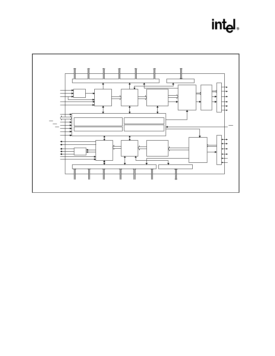
LXT6051 -- STM-1/0 SDH Overhead Terminator
24
Datasheet
After frame synchronization and de-scrambling, the Regenerator Section Termination (RST)
extracts the RSOH:
�
The expected value of the J0 string is stored via the microprocessor interface. The received J0
string is compared with the stored version, and also used to calculate a CRC-7 byte. Two
alarms can be generated: a J0 (Trace ID) Mismatch alarm and J0 CRC-7 mismatch alarm.
�
B1 byte is calculated internally and compared to the incoming B1 value. The errors are stored
into a set of counters that can be read by the microprocessor interface.
�
E1 is provided serially at the RROW output.
�
F1 is provided serially at the RMOW output. E1 and F1 are synchronous and can be accessed
using the 64 KHz clock provided at RROWC and the 8 KHz synchronization pulse provided at
RROWBYC.
�
D1-D3 are provided serially at the RRD output. The 192 KHz clock reference for this output is
provided at RRDC.
�
Next the Multiplexer Section Termination (MST) extracts the MSOH:
�
K1 and K2 bytes are provided via both a microprocessor register and serially at the RSOH
output. A filter based on 3 consecutive identical values of K1 and K2 gates the update of the
microprocessor registers.
�
D4-D12 bytes are provided serially at the RMD output. The 576 KHz clock reference for this
output is provided at RMDC.
Figure 3. LXT6051 Block Diagram
WR/RW
Communication Overhead
MST/MSP
Multiplexer
section
Demultiplexer
Pointer
Interpretation
Microcontroller Interface
Intel/Motorola Selectable
DEMUX Timing Generator
MUX Timing Generator
Overhead RAM
HOA Higher
order Path
Termination
A<7:0>
DATA<7:0>
DHICLK
Communication Overhead
T
e
l
e
c
o
m
B
u
s
Inter
f
ac
e
MSP Interface
MCUTYPE
RST
RST
Regenerator
Section
termination
HOA Higher
order Path
Termination
Te
l
e
c
o
m
B
u
s
I
n
t
e
r
f
a
c
e
MSP Interface
B3ZS
Decoder
MSA/MSP
MST
Multiplexer
section
HCS Higher
order
Connection
Supervision
MHBDATA<7:0>
RST
Regenerator
Section
termination
B3ZS
Encoder
RSOH & MSOH
SERIAL ACCESS
HPOH
SERIAL
ACCESS
E1 E2 F1
ACCESS
F2 F3
ACCESS
D1 D3
ACCESS
D4 D12
ACCESS
RSOH & MSOH
SERIAL ACCESS
HPOH
SERIAL
ACCESS
E1 E2 F1
ACCESS
F2 F3
ACCESS
D1 D3
ACCESS
D4 D12
ACCESS
Retiming
Function
DHPOSD/DHNRZ
DHNEGD
MHPOSD/MHNRZ
MHNEGD
MICLK
MHBCLK
MHICLK
MSP
Interface
MSP interface
DHBDATA<7:0>
DHBCLK
MHBCLKO
RD/E
CS
AS

STM-1/0 SDH Overhead Terminator -- LXT6051
Datasheet
25
�
S1 is provided via both a microprocessor register and serially at the RSOH output. A filter
based on 3 consecutive identical values of S1 gates the update of the microprocessor register.
�
M1 is provided serially at the RSOH output and updates MST REI counters accessible by the
microprocessor.
�
E2 is provided serially at the RMOW output. The
64 KHz clock reference for this output is provided at RROWC and the 8 KHz sync pulse at
RROWBYC.
�
B2 byte is calculated internally and compared to the incoming B2 value. The errors are stored
into a set of counters that can be read by the microprocessor interface. These errors are also
inserted in the transmitted M1 byte if enabled (see register 60H).
The Multiplexer Section Protection (MSP) block allows the selection of data presented to the
Master Multiplexer Section Adaptation (MSA) block to come from either the "Master MST output
data" or "Slave MSP output data" (see
Figure 7
or
"Multiplexer Section Protection (MSP) Block"
on page 40
). The choice is completely under the control of the microprocessor. The microprocessor
has access to all the Master and Slave data (K1/K2 bytes, error statistics derived from counters and
alarm status from both chips) necessary for making this decision.
The MSA block interprets the H1-H3 payload points bytes to determine the location of the VC-3 or
VC-4 payload structure. Positive and negative pointer movement events are stored in counters that
can be accessed via the microprocessor interface. The data from the MSA section is then output to
the HPT section in a byte parallel format.
The HPT section extracts the HPOH:
�
The expected value of the 16 on 64 byte J1 string is stored internally via the microprocessor
interface. The receive value of J1 is compared with the stored version, and is also used to
calculate a CRC-7 byte (in 16 byte string configuration). Two alarms are generated: a J1
Mismatch alarm and J1 CRC-7 mismatch alarm.
�
B3 byte is calculated internally and compared to the incoming B3 value. The errors are stored
into a set of counters that can be read by the microprocessor interface. These errors are also
inserted in the transmitted G1 REI bits (G1<7:4>) if enabled (see registers 70H and 71H).
�
F2 and F3 are provided serially at the ROW1 and ROW2 outputs. The 64 KHz clock reference
for this output is provided at RPOWC and the 8 KHz sync pulse at RPOWBYC.
�
C2 is provided via both a microprocessor register and serially at the RPOH output. The C2
value provided via a microprocessor register is filtered over 3 or 5 frames. The number of
filtering frames can be programmed by the microprocessor.
�
G1 is provided serially at the RPOH and is used to update HPTREI-CNT registers accessible
by the microprocessor.
�
K3 is provided via both a microprocessor register and serially at the RPOH output.
�
The last block is the re-timing block. This block allows the alignment of the receive payload
with the external signal DRETFRMI, which supplies the J0 position and an external clock
DRETCLK. A new value of the pointer based on the new alignment position is assigned to the
payload. This block typically is bypassed for a multiplexer application. It is typically only
required for external re-timing and alignment of multiple TUG-3 payload signals.
The output of this block is then sent to the Receive Telecom Bus DTBDATA<7:0> with the
DTBCLK clock and reference timing DTBJ0J1EN and DTBPAYEN.

LXT6051 -- STM-1/0 SDH Overhead Terminator
26
Datasheet
3.2.1
Reference Clocks
The transmit and the receive side of the LXT6051 operate independently. In the STM-0 case, the
input and output can either be serial or parallel. In the STM-1 case, the input and output are parallel
only. The following table shows the clock connections required for STM-1 and STM-0:
3.3
Modes of Operation
3.3.1
Chip Configuration
The LXT6051 can be programmed in seven different configurations in STM-0 or STM-1 mode
(see register 50H.)
�
Repeater mode
�
Terminal Mode No Protection
�
Terminal Mode Protection Main
�
Terminal Mode Protection Slave
�
Add And Drop Mode No Protection
�
Add And Drop Mode Protection Main
�
Add And Drop Mode Protection Slave
Note that the following are examples of configurations. For more details, please refer to
Application Note LXT6051 and LXT6251A SDH Chipset.
3.3.2
Repeater Mode Configuration
All MSOH, HPOH and VC data is passed through internally and no off chip connection is required
between the transmit and the receive sides. The transmit source of the RSOH bytes is configurable
(see register 60H).
Figure 4
is an example of an STM-0 repeater using the serial interface. The timing is recovered by
the high-speed line interface unit and passed to the transmit side via the LXT6051. In the event of a
receiver failure (i.e., a LOS of Signal Alarm), the LXT6051 will switch to a Blue signal reference if
so configured (see register 40H).

STM-1/0 SDH Overhead Terminator -- LXT6051
Datasheet
27
3.3.3
Terminal Mode Configuration (No Protection)
In
Figure 5
the LXT6051 is used with the LXT6251A for the implementation of an STM-1
terminal multiplexer. The LXT6251A is a 21 E1 mapper designed to accommodate 21 E1
tributaries in a single chip. The LXT6051 and the LXT6251A communicate via the Telecom Bus.
In an STM-0 configuration a single 21 E1 multiplexer is required. In an STM-1 Terminal
Multiplexer, three 21 E1 mappers are required, sharing the telecom bus to implement a full 63xE1
MUX Telecom bus.
Figure 4. STM-0 Repeater Application
Table 4. Repeater Clocks
STM-0
STM-1
Multiplexer serial clock
input
MHICLK (51.84
MHz)
Not used
Multiplexer parallel
clock input
MHBCLK (6.48
MHz)
MHBCLK (19.44
MHz)
Demultiplexer serial
clock input
DHICLK (51.84
MHz)
Not used
Demultiplexer parallel
clock input
DHBCLK (6.48
MHz)
DHBCLK (19.44
MHz)
NOTE: DRETFRMI and DRETCLK are used when a re-timing
function is implemented on the receive side.
LXT6051
Regenerator configuration
SSI 7200
Line
Interface
STM-0
B3Zs
encoded
Los Alarm
51.84Mbit/s
Microprocessor
for configuration and
network management
interface
51.84 MHz +/- 20 ppm Local
Refernce for Blue signal
Generation
B1
Error
B2
Error
J0
E1
F1
D1 to
D3
Pass Through programmable
Serial Clock
Serial Data
SSI 7200
Line
Interface
Serial Clock
Serial Data
STM-0
B3Zs
encoded
51.84Mbit/s
LXT
6051_.
FM
-
PAGE
-1 - 7/8/99

LXT6051 -- STM-1/0 SDH Overhead Terminator
28
Datasheet
3.3.3.1
Receive Side Telecom Bus Timing Source
In the Terminal mode, when receive re-timing is disabled (see register 51H), the receive side
telecom bus timing is derived from the "recovered" clock.
Assuming an inactive LOS, the "recovered" clock is derived from DHICLK in serial mode and
DHBCLK in parallel mode. During an active LOS condition, if configured (see register 40H), the
"recovered" clock is derived from MHICLK in serial mode and MHBCLKI in parallel mode (used
as "blue" clocks).
When receive re-timing is enabled, the receive side telecom bus timing is derived from the re-
timing clock (DRETCLK).
This arrangement of the LXT6051 providing both timing and data (at the receive telecom bus) is
referred to as co-directional timing.
3.3.3.2
Transmit Side Telecom Bus Timing Source
The transmit side telecom bus timing is provided by the LXT6051. It is derived from the local
clock reference (MHICLK in serial mode and MHBCLKI in parallel mode). This arrangement of
the LXT6051 providing the timing and receiving the data (at the transmit telecom bus) is referred
to as contra-directional timing.

STM-1/0 SDH Overhead Terminator -- LXT6051
Datasheet
29
3.3.4
Add and Drop Configuration
In
Figure 6
the LXT6051 is used with the LXT6251A for the implementation of an STM-1 Add/
Drop multiplexer with 42 E1 access (63 is possible with the addition of another LXT6251A).
3.3.4.1
Receive Side Telecom Bus Timing Source
Receive side telecom bus timing in the ADM case is identical to the terminal case.
3.3.4.2
Transmit Side Telecom Bus Timing Source
In an ADM configuration, the transmit side telecom bus timing is provided to the LXT6051.
Therefore the timing at the transmit telecom bus is co-directional, since both timing and data are
provided to the LXT6051. STM-1 ADM Configuration With 42 E1 Access
Figure 5. STM-1 Terminal Multiplexer
21 E1 card TUG#3
21 E1 Card Tug#2
21 E1 Card Tug#1
LXT6051
OHT
TX
LXT6051
OHT
RX
LXT6251A
Mapper
TX
LXT6251A
Mapper
RX
MSOH:
M1 REI,
K2 RDI
HPOH:
G1 REI, G1
RDI
REI, RDI
Alarm Status
Telecom Bus Data
Telecom Bus Data
Transmit Data and Clock E1 <1:21>
Receive data and Clock E1 <1:21>
Telecom Bus Timing
Telecom Bus Timing
SAP
RAP
STM-1
LIU
E1 Line
Interface
units
SETS Local Reference 19.44 MHz
Data
Data
Clock
Clock
TX/RX STM-0
LOS
STANDARD Terminal
STM-1 configuration
without Receive retiming
LXT6251A
Mapper
TX
LXT6251A
Mapper
RX
REI, RDI
Alarm Status
Transmit Data and Clock E1 <1:21>
Receive data and Clock E1 <1:21>
SAP
RAP
E1 Line
Interface
units
LXT6251A
Mapper
TX
LXT6251A
Mapper
RX
REI, RDI
Alarm Status
Transmit Data and Clock E1 <1:21>
Receive data and Clock E1 <1:21>
SAP
RAP
E1 Line
Interface
units
Transmit
Reference

LXT6051 -- STM-1/0 SDH Overhead Terminator
30
Datasheet
3.3.4.3
Updating the Transmit AU Pointer Justification Event
Counters
If the re-timing function on the receive side is disabled, re-clocking by the local clock will occur on
the transmit side of the LXT6051. If the receive and local (which generates the transmit clock)
clocks are slightly different, pointer movements on the transmit side of the LXT6051 will be
generated. These pointer movements will be reflected in the transmit AU pointer justification event
counters.
If the re-timing function is enabled, re-clocking will take place on the receive side. Similarly, if the
receive and the local (which generates DRETCLK and transmit clock) clocks are slightly different,
pointer movements are again generated on the transmit side of the LXT6051 and reflected in
transmit AU pointer justification event counters.
Figure 6. STM-1 ADM Configuration With 42 E1 Access
LXT6251A 21 E1 card
LXT6051
OHT
RX
LXT6251A
21E1 RX
LXT6051
OHT
TX
RX
TX
LXT6251A
21E1 TX
EAST
WEST
Pass Trough TU-12's,
TUG3 #3, Timing
Telecom
Bus Timing
& Clock
Telecom Bus Timing
LXT6251A
21E1 RX
LXT6251A
21E1 TX
Telecom Bus Data
TUG3 #1
TUG3 #2
Pass Trough TU-12's
Telecom Bus Data
PTTUGA
PTTUGB
PTSOH
PTTUGA
PTTUGB
PTSOH
GND
DTBTUG1
DTBTUG3
VCC
GND
Insert E1
DTbTugEn
DTbTugEn
DTBTUG2
LXT6051
OHT
TX
LXT6251A
21E1 TX
LXT6051
OHT
RX
RX
LXT6251A
21E1 RX
Pass Trough TU-12's,
TUG3 #3, Timing
LXT6251A
21E1 TX
LXT6251 21E1
RX
TUG3 #1
TUG3 #2
Pass Trough TU-12's
PTTUGA
PTTUGB
PTSOH
DTbTugEn
DTBTUG2
TX
LXT
6051_.
FM
-
PAGE
-1 - 7/8/99
Telecom Bus Clock
PTTUGB
PTSOH
DTbTugEn
PTTUGA

STM-1/0 SDH Overhead Terminator -- LXT6051
Datasheet
31
3.3.5
Terminal Protection Mode
Figure 7
describes the dataflow for a 1-for-1 terminal protection configuration. The protection
mode is an implementation of the ITU specifications in 1-for-1 configuration.
The LXT6051 can be used either in the main (master) or the redundant (slave) signal path. The
master & slave signal paths are connected via the MSP bus.
In the master configuration the LXT6051 is connected to the LXT6251A via the telecom bus in
both the transmit and the receive directions.
In the slave configuration the LXT6051 is indirectly connected to the LXT6251A via the MSP bus
in both the transmit and the receive directions.
3.3.5.1
Receive Side Telecom Bus Timing Source
On the receive side, the master LXT6051 selects the data from either its receive MST block or its
receive MSP bus (fed by the slave) and presents this selection using a co-directional timing
arrangement at the receive telecom bus interface. If the MSP (slave) data is selected (i.e., the
protection switch is active, see register 21H) the clock provided at the receive telecom bus will be
derived from either DMSPPCKI (demultiplexer protection clock) or, if retiming is enabled,
DRETCLK (demultiplexer retiming clock, see register 51H).
3.3.5.2
Transmit Side Telecom Bus Timing Source
On the transmit side, the master LXT6051 feeds the data received from its transmit telecom bus to
both its MST block and MSP block (which feeds the slave) using a contra-directional timing
arrangement at the transmit telecom bus interface.
Co-directional timing arrangement is used in both the receive and transmit directions at the MSP
interface.
3.3.6
Receiver Default Operation
Figure 8
is a block diagram of the receive section of the LXT6051. The detailed description follows
the data flow from left to right and describes the functionality and configuration of each block.
Note that all status change alarms, counter overflow alarms and receive byte change alarms
mentioned, can cause the INT output pin to be activated if they are unmasked. Please refer to the
register definition for location of alarms, masks & interrupts.
3.3.6.1
Serial Interface
The serial interface block accepts an STM-0 input as a B3ZS encoded or NRZ signal. The B3ZS
signal is input at DHPOSD and DHNEGD and the NRZ signal is input at DHPOSD. The 51.84
MHz clock is input at DHICLK.
A bipolar violation detector has been implemented in the B3ZS decoder. Detection of a BPV is
indicated in register A0H. Note that the selection (see register 50H) of the serial interface and
B3ZS encoder and decoder is common to both the transmit and receive sides of the chip.
A filter for the LOS input is provided by the line interface circuit (register 40H). The filtering on
the LOS can be integrated over 128 or 4096 clock cycles. A LOS status change is indicated in
register A0H.

LXT6051 -- STM-1/0 SDH Overhead Terminator
32
Datasheet
3.3.6.2
Parallel Interface
The parallel interface block accepts a byte format input at DHBDATA<7:0> in STM-0 or STM-1
mode. No specific order on the byte is required for the LXT6051 to operate. The parallel clock is
input at DHBCLK. As in the serial case, the selection (see register 50H) of a parallel interface is
common between transmit and receive sides.
A filter for the LOS input is provided by the line interface circuit. The filtering on the LOS can be
integrated over 16 or 512 clock cycles. An LOS status change is indicated in register A0H.
Figure 7. Terminal Protection Mode Data Flow
LXT6051 Receive Section Main Channel
MST
Multiplexer
section
HPT
High Order
Path Section
Te
l
e
c
o
m
Bu
s
I
n
t
e
r
f
a
c
e
MSP Interface
B3ZS
Decoder
LXT6051 Receive Section Slave channel
MST/MSP
Multiplexer
section
MSP Interface
LXT6251A
21 E1 Mapper
MSP
Protection
switch
MSA
Pointer
Recovery
Re-
Timing
Receive
STM-0
Slave
Receive
STM-0 Main
RST
Regenerator
Section
RST
Regenerator
Section
B3ZS
Decoder

STM-1/0 SDH Overhead Terminator -- LXT6051
Datasheet
33
Figure 7. Terminal Protection Mode Data Flow
LXT6051Transmit Section Slave Channel
MSP Inte rface
RST
Rege nerator
S ecti on
B 3ZS
Encode r
LXT6051 Transmit Section Main Channel
MSP Inte rface
Te
l
e
c
o
m
B
u
s
In
t
e
r
f
a
c
e
MST
M ul ti pl exer
S ecti on
RST
Re ge nerator
S ecti on
B 3ZS
En cod er
LXT6251A
21 E1 Mapper
Transmit STM-0 Slav e
Transmit STM-0 Main
MSA
P oi nter
P ro cessi ng
HPT
Hig h O rd er
Pa th Se cti on
MST
M u lti pl exer
S ecti on

LXT6051 -- STM-1/0 SDH Overhead Terminator
34
Datasheet
3.3.6.3
Clock Distribution and Reference
Two separate inputs are supplied for Blue clock references.
�
MHICLK is used for a serial reference clock in the case of an STM-0 system. The frequency
of a serial reference clock is 51.84 MHz �20ppm
�
MHBCLKI is used for a parallel reference clock in the case of either an STM-0 or an STM-1
system. The frequency of the parallel reference clock for STM 0 is 6.48 MHz �20ppm and for
STM-1 19.44MHz �20ppm
An active LOS can have two consequent actions that can be enabled or disabled (see register 40H):
�
Clock switches from receive clock to reference clock
�
Insert AIS towards the PDH network from the RST section
3.3.6.4
Framer
The framer operates on either a parallel byte or a serial bit stream. Two settings are available for the
frame acquisition state machine. One follows ITU-T G.783; the other is shown in
Figure 9
.
Figure 8. LXT6051 Receiver Blocks
Receive side LXT6051
Serial Interface
Parallel
Interface
Framer
Regenerator
Section
receiver
Multiplexer section
receiver
MSP block
Pointer
processing
Retiming
Function
Higher order
path Receiver
RSOH
Interface
MSOH Interface
Clock
distribution and
references
DHPOSD
DHNEGD
DHICLK
DHBDATA[7..0]
DHBCLK
RS
O
H
RS
O
H
E
N
RS
O
H
F
R
SERIAL
RSOH
&MSOH
RR
O
W
RO
W
C
RO
W
B
Y
C
B1
O
U
T
LO
F
OO
F
RRD
RM
DC
RM
D
R
RDC
RM
O
W
B2
O
U
T
RPOHEN
RPOHCK
RPOH
B3OUT
ROPHFR
DTBH4EN
DTBPAYEN
DTBTUGEN 1 TO 3
DTBPAR
DTBCK
DTBJ0J1EN
DHBDATA[7..0]
SD
SF
B2
O
U
T
MSP INTERFACE
DM
S
P
P
C
K0
DM
S
P
P
C
KI
D
M
SP
PJ
0
E
N
D
M
SP
PA
U
E
N
D
M
SPP
SF
D
M
SPP
SD
DM
S
P
P
DAT
A
[
7
.
.
0
]
DRETCLK
DRETFRMI
RPOW2
RPOWBYC
RPOW1
RPOWC
RD
O
W
LOS
MHICLK
MHBCLKI
ST
M
M
O
D
E
SC
R
A
M
S
E
L
DRAWING
1 -
RECEIVE
SECTION
OHT
DETAILS
- 7/9/99
AISRX

STM-1/0 SDH Overhead Terminator -- LXT6051
Datasheet
35
Frame Acquisition Algorithm
The frame acquisition algorithm is done on byte-wide key word identification. The framer
eliminates the eight phases (bits) of ambiguity and memorizes the position of the frame word. The
framer also identifies the position of the new data flag (NDF).
Two consecutive frames with correct frame words and identical NDF are required to change from
an Out Of Frame State (OOF) to an In Frame State (INF). To declare an OOF condition, four
consecutive frames with incorrect frame words are required.
For certain values of the HPOH pointer, "R" bits in the VC12 container in STM-0 will look like a
framing word after scrambling. This results in false frame synchronization. To eliminate this
problem, the acquisition machine is configurable (see register 40H).
The robust configuration requires five consecutive frames with identical NDF and two consecutive
frames with the correct frame word for frame acquisition. This will minimize the probability of
incorrect synchronization. To ensure that an OOF condition is activated when an incorrect
synchronization occurs, the state machine will desynchronize when eight consecutive frames not
having identical NDF bits.
Upon frame acquisition, the framer de-scrambles the signal. The standard scrambler defined by the
ITU is (2
7
�1). Two additional scramblers (2
11
-1) and (2
13
-1) can be programmed for STM-0 and
STM-1 (see register 50H). This flexibility allows the optimum choice of scrambler for a radio
application where an equal distribution of 1s and 0s is required.
Figure 9. STM-0 Robust Frame State Machine
Locked In
Frame
In Frame
Out Of
Frame
8 consecutive frames
with Invalid NDF
4 consecutive frames
with Errored FAS
2 consecutive frames
with Correct FAS and Valid NDF
Received
Frame with
Invalid NDF
check 3 more consecutive
frames with Valid NDF
ROBUST ALGORITHM FOR STM-0 FRAMING
Desynchronisation:Transition from Locked In Frame to Out Of Frame
Acquisition
:Transition from Out Of frame to In Frame State.
Transition
:Transition from In Frame State to Locked In Frame.
OOF Alarm is disabled and receive demultiplexer is re-synchronized, according to the new
frame boundary, when entering in the In Frame State.
OOF Alarm is activated and receive demultiplexer keeps its former synchronization when
entering in the Out Of Frame State.
Correct FAS : STM-0 Frame detected : A1A2 bytes = Hex "F628"
Errored FAS : Errored Frame (errors on A1A2 bytes)
Valid NDF
: Valid New Data Flag can be either: descrambled HEX "6" "9" or "F" for NDF or AIS
Invalid NDF = Invalid receive New Data Flag ( State other than the 3 valid ones)

LXT6051 -- STM-1/0 SDH Overhead Terminator
36
Datasheet
Loss of Frame (LOF) Detection
Upon detection of an Out Of Frame condition, no consecutive action is required by the ITU
specifications. The number of Out of Frame events are counted and stored in a 13-bit counter
accessible via registers 43H and 44H.
The Loss Of Frame state machine can be configured via the registers 41H and 42H. Three
parameters are programmable (from 1 to 32 frames) in the state machine:
M is the number of consecutive frames with no Out Of Frame conditions required to re-enter a
normal state. N is the number of consecutive frames with no Out Of Frame conditions required to
re-enter a normal state from a Loss Of Frame state. L is the number of non-consecutive frames with
Out Of Frame conditions required to enter a Loss Of Frame state.
Status changes in the OOF & LOF detectors generate OOF & LOF alarms. Also, output from these
detectors is provided at the OOF & LOF output pins.
3.3.6.5
Regenerator Section Receiver
This section provides access to all Regenerator Section Overhead Bytes. All the overhead bytes (27
in STM-1 and 9 in STM-0) are accessible at the RSOH serial output.
Figure 10. LOF State Machine
NORM
STW
LOF
OofSt = 0
OofSt = 1
N
consecutive
frames with
OofSt = 0
L
non-consecutive
frames with
OofSt = 1
M
consecutive
frames with
OofSt = 0
OofSt = 1

STM-1/0 SDH Overhead Terminator -- LXT6051
Datasheet
37
The Regenerator Section Trace J0
This byte is used to repetitively transmit a Section Access Identifier so that a section receiver can
verify its continued connection to the intended transmitter. This byte has been defined in the latest
specification of ITU. To avoid compatibility problems with in-service equipment, the chip can
ignore J0 processing via register 51H.
The expected J0 string is configurable (see registers 0EH and 0FH). This J0 string value needs to
have the correct CRC7 bits per G707 specifications. The receiver calculates the CRC7 of the
received J0 string. In the case of a mismatch between the expected & received J0 string, a J0
mismatch (J0MsMtch) is indicated in register A1H. In the case of a transmission error in the J0
string, a J0 string CRC7 error (J0Crc7Err) is indicated in register A1H and will mask the
J0MsMtch alarm.
Bip-8 B1 Byte
This byte is used for Regenerator Section error monitoring. The error events are counted in a 16 bit
counter accessible via registers 45H and 46H.
The B1 counter can be configured as either a bit or a block counter (see register 47H). Also, the
B1OUT output provides pulse for each calculated B1 bit that is different from the one received.
E1 Orderwire Byte
This 64 Kbit/s channel is used to provide orderwire channel for voice communication. The data is
serially accessible via RROW. The 64 KHz clock and the 8 KHz byte synchronization signals are
used to receive both the E2 and F1 bytes and are provided at pins ROWC and ROWBYC.
Figure 11. Overhead Bytes for the STM-1
A1
A1
A1
A2
A2
A2
J0
B1
E1
F1
D1
D2
D3
AU Pointers
B2
K1
K2
D4
D5
D6
D7
D8
D9
D10
D11
D12
S1
M1
E2
B2
B2
RSOH
MSOH
Reserved for National Use
Media dependant Byte
Undefined Bytes

LXT6051 -- STM-1/0 SDH Overhead Terminator
38
Datasheet
F1 Byte
This 64 Kbit/s channel is reserved for the user's purpose. It can be used as an extra maintenance
orderwire access. The data is serially accessible via RDOW. The 64 KHz clock and the 8 KHz byte
synchronization signals are used to receive both the E1 and E2 bytes and are provided at pins
ROWC and ROWBYC.
D1 to D3 Data Channels
This 192 Kbit/s channel is used by the network management as a data channel. The data is
accessible via pin RRD and the clock is provided by RRDC. Note that ROWBYC can be used as an
8KHz synchronization if required.
Receive Regenerator Section AIS (RstAIS)
The AIS generated after the Regenerator Section is labeled RstAis. It can be inserted on the
following conditions:
�
Loss Of Signal (LOS)
�
Loss Of Frame (LOF)
�
Trace Identification Mismatch (J0MsMtch)
These conditions can be individually enabled or disabled (see register 40H). A test register that can
force an RstAis for test purposes is also available. RstAis insertion is indicated in register D0H.
National Used Bytes
The four RSOH "National Use" bytes are only accessible in the STM-1 case. These bytes can be
read via registers 03H, 04H, 05H, and 06H or serially at the RSOH output.
Media Dependent and Undefined Bytes
The six "Media Dependent" and four "Undefined" bytes are only accessible in the STM-1 case.
These bytes can only be read via the serial RSOH output.
3.3.6.6
Multiplexer Section Receiver
The Multiplexer Section receiver handles the MSOH overhead bytes. All the overhead bytes (45 in
STM-1 and 15 bytes in STM-0) are accessible at the RSOH serial output.
B2 Error Byte
This byte is used for Multiplexer Section error monitoring. The B2 errors are counted either as
block error in register 10H and 11H (13 bit) or as bit errors in register 12H, 13H and 14H (18-bit
counter).
An Excessive Error Defect (EED) indication (see register A1H) is generated by integrating the B2
errors in a sliding window. Integration is also used when clearing the EED indication. Six registers
allow the configuration of EED indication thresholds. They are 18H, 15H, 16H, 17H, 1EH, 1BH,
1CH and 1DH.

STM-1/0 SDH Overhead Terminator -- LXT6051
Datasheet
39
These six registers allow configuring the EED threshold from a bit error rate of 10-3 to a bit error
rate of 10-9, even in the case of a non-Gaussian statistical distribution of errors. An active EED
indication can be configured to insert an AIS signal (see register 20H).
K1 and K2 Bytes: Automatic Protection Channel
These bits are assigned for the APS signaling. A change in K1 byte for three consecutive frames is
indicated in register A1H and allows the updating of register 00H. A change in K2 byte for three
consecutive frames is indicated in register A1H and allows the updating of register 01H.
MS-RDI via K2 Byte
The Multiplex Section Remote Defect Indication (MS-RDI) is used to tell the transmit end that the
received end has detected an incoming section defect or is receiving MS-AIS. An MS-RDI is
detected when the three received K2<2:0> bits have a value of "110" for three consecutive frames.
MS-RDI detector status changes are indicated in register A1H.
MS-AIS via K2 Byte
The Multiplex Section AIS is detected when the three received K2<2:0> bits have a value of "111"
for three consecutive frames. MS-AIS detector status changes are indicated in register A1H.
MS-REI via M1 Byte
This byte is allocated for the Remote Error Indication. Remote BIP errors are accumulated in a 13-
bit counter, accessible via registers 0AH and 09H. Remote block errors are accumulated in an 18-
bit counter, accessible via registers 0DH, 0CH and 0BH.
S1 Byte: Synchronization Status
S1<3:0> bits are allocated for Synchronization Status Messages. A change in S1 byte for three
consecutive frames is indicated in register A2H and allows the updating of register 02H.
National Used Bytes
The "National Use" bytes are only accessible in the STM-1 case. There are two MSOH "National
Use" bytes. These bytes can be read via registers 07H and 08H.
Undefined Bytes
The "Undefined Bytes" are only accessible in the STM-1 case. There are 26 bytes only accessible
via the RSOH serial output.
E2 Byte: Orderwire Channel
This 64 Kbit/s channel is used to provide orderwire channel for voice communication. The data is
accessible serially via RMOW. The 64 KHz clock and the 8 KHz byte synchronization signals are
used to receive both the E1 and F1 bytes and are provided at pins ROWC and ROWBYC.

LXT6051 -- STM-1/0 SDH Overhead Terminator
40
Datasheet
D4 to D12 Bytes: Data Channel
This 576 Kbit/s channel is used as a data channel by the network management. The data is
accessible via pin RMD and the clock is provided by RMDC.
Receive Multiplexer Section AIS (MS-AIS)
The AIS generated after the multiplexer section is labeled MstAis. It can be inserted on the
following conditions:
�
MS-AIS detection in K2
�
EED detection
The AIS insertion can disabled or forced via register 20H. The EED dependency can be disabled
via register 20H (ITU specification). MstAis insertion is indicated in register D0H.
3.3.6.7
Multiplexer Section Protection (MSP) Block
Master 1-for-1 Protection Configuration
The MSP block receives the data coming from the MST block and from the slave receiver via the
DMSPPDATA<7:0> inputs (MSP bus). K1 and K2 from the MSP bus are de-multiplexed and
accessible in registers 22H and 23H. The Signal Degrade (SD) and the Signal Fail (SF) indications
from the slave are input to the Master at DMSPPSD & DMSPPSF respectively and are accessible
in register C3H.
Changes in register 22H, 23H, DMSPPSD or DMSPPSF are indicated in register A3H.
Having access to the K1 and K2, SD and SF information for both the master and the slave
LXT6051, the microprocessor can select the appropriate working channel. The selection is done by
setting the protection switch via register 21H. The effective switch position is accessible on register
D0H.
K1/K2 filtering and SF detection are done on chip. The SD detection is done by the microprocessor
using a user defined criteria.
Slave 1-for-1 Protection Configuration
This block is just an interface between the data received from the MST block and the MSP
interface with the Master. All switching is done in the master-configured LXT6051.
3.3.6.8
Pointer Recovery
Pointer Recovery Block
The pointer recovery block interprets the value of the incoming pointer associated with either a
VC-3 (STM-0) or a VC-4 (STM-1) payload. The AU pointers include two SS undefined bits. These
bits can be either ignored or recovered in the receive pointer processor (see register 90H). The
monitoring function of the receive pointer processor includes the following counters:
�
An 11-bit Positive Justification Counter accessible via register 91H and 92H
�
An 11-bit Negative Justification Counter accessible via register 93H and 94H

STM-1/0 SDH Overhead Terminator -- LXT6051
Datasheet
41
This block indicates the following conditions via register A4H: an AU-AIS (all ones in the
pointer), Loss of Pointer (LOP) or New Data Flag (NDF).
The LOP detection follows the ITU G 783 recommendation using eight consecutive frames.
Receive Adaptation Section AIS (DmsaAIS)
The AIS generated after the Pointer recovery section is labeled DmsaAis. It can be inserted on the
following conditions:
�
AU-AIS detection (all ones pointer for three consecutive frames)
�
LOP detection
The AIS can be disabled or forced via register 90H. DmsaAis insertion is indicated in register
D0H.
3.3.6.9
Higher Order Path Receiver
The Higher Order Path Receiver processes the overhead bytes associated with the Higher Order
Path Overhead. All the Path Overhead bytes are accessible at the RPOH output.
J1 Byte Path Trace
This byte is used to repetitively transmit a Path Access Identifier so that a path receiver can verify
its continued connection to the intended transmitter. The length of the "expected" J1 string can be
programmed to either 64 bytes (non-specified) or 16 bytes with CRC7 (see register 80H). The 16
byte "expected" J1 string value needs to have the correct CRC7 bits per G707 specifications. The
receiver calculates the CRC7 of the received J0 string.
In the case of a mismatch between the expected and received J1 string, a J1MsMtch is indicated in
register A5H. In the case of a transmission error in the J1 string, a J1Crc7Err is indicated (16 byte
case only) in register A5H and will mask the J1MsMtch indication.
B3 Byte
This byte is used for Higher Order Path error monitoring. The error events are counted in a 16 bit
counter accessible via registers 86H and 87H.
The B3 counter can be used either as a bit or a block counter configurable via register 80H. Also,
the B3OUT output provides a pulse for each calculated B3 bit that is different from the received
one.
C2 Byte
This byte indicates the composition of the VC-3 or the VC-4 payload. A change in the C2 byte for
three or five (configurable via register 80H) consecutive frames is indicated in register A4H and
allows the updating of register 83H.
An "expected" value of C2 can be programmed in register 82H. If the received C2 value is not
equal to the expected value and is not zero or one, this is indicated in register A5H via the HptSlm
(HPT Signal Label Mismatch).

LXT6051 -- STM-1/0 SDH Overhead Terminator
42
Datasheet
VC-AIS is defined as all ones in C2 (new G783 specifications). Five consecutive frames are
required for the VC-AIS detection which is indicated in register A4H.
Unequipped Detection
To generate an "unequipped" indication, a set of four simultaneous events need to be detected (see
register 81H):
�
C2 equal to all zero
�
J1 equal to zero
�
N1 equal to all zero
�
No B3 errors
The unequipped detector requires 5 frames before it is indicated in register A5H.
G1 Byte
This byte conveys the path status and performance back to a VC-3 or VC-4 trail termination source
as detected by a trail termination sink.
G1<7:4> bits act as a Remote Error Indication (REI). They report the number of B3 errors detected
at the remote end. These REI errors are accumulated in the REI counter registers 88H and 89H.
The REI counter can be selected as a bit counter or as a block counter via register 80H.
G1<3:1> bits act as a Remote Detection Indication (RDI). They, along with G1<0> ("spare" bit),
are accessible via register 85H. The contents of this register is filtered over 3 or 5 frames
configurable via register 80H. An update to register 80H is indicated in register A5H.
An RDI is reported to the far-end upon detection of an SLM (C2 Mismatch) or an "unequipped"
alarm. The dependency of RDI on either of these conditions is configurable via 81H. This will
ensure compatibility of the new equipment with an installed equipment base. (See Table 5).
K3 Byte
This byte is allocated for the VC-3 and VC-4 Automatic Protection Switching (APS). A change in
K3 byte for three consecutive frames is indicated in register A4H and allows the updating of
register 84H.
N1 Byte
There is no internal processing for the tandem connection byte. This is because in an ADM, the
virtual container VC-3 or VC-4 is de-multiplexed to VC12 to extract and insert the VC-12 traffic.
A new B3 needs to be generated and the tandem connection is broken.
N1 is accessible at the RPOH output and can be used in the detection of an "unequipped" VC (see
register 81H).

STM-1/0 SDH Overhead Terminator -- LXT6051
Datasheet
43
F2 and F3 Bytes
These two 64 Kbit/s channels are reserved for the user. They can be used as an extra maintenance
orderwire access. The data is serially accessible via the RPOW1 pin for F2 and RPOW2 for F3.
The 64 KHz clock and 8KHz synchronization are provided on pins RPOWC and RPOWBYC. In
an ADM configuration with no receive timing, these bytes can be passed through to the transmit
side.
H4 Processing and Multi-Frame Recovery
The multi-frame recovery state machine requires two consecutive frames with the correct H4
adjacent pattern to synchronize. The Loss of Multiframe (LOM), indicated in register A5H, is
declared after two multi-frames. The LOM indication forces the DTBH4EN output on the Telecom
Bus Low.
Receive Higher Order path AIS (HptAIS)
The AIS generated after the HPOH receiver is labeled HptAis. It can be inserted on the following
conditions:
�
SLM (C2 byte mismatches)
�
TIM (J1 string mismatches)
�
Unequipped detection
The AIS can be disabled or forced via register 80H.
3.3.6.10
Re-Timing Function
The re-timing function block is used when the system needs to synchronize the DTBDATA<7:0>
output with a local clock input. Re-timing can be disabled via register 51H.
Two external signals are required to align the payload:
�
DREFRMI, an 8 KHz input signal indicating the position of the J0 byte. This input is always
needed.
�
DRETCLK, a 19.44 MHz input signal for a STM-1 or a 6.48 MHz input signal for STM-0.
This is the "local" clock.
The DRETFRMI is generated externally by DRETCLK. The re-timing function recalculates the
new pointer and inserts the new value to the payload VC-3 and VC-4.
After the re-timing block, the signal is sent to the Telecom Bus. The Telecom Bus is described in
the Timing Specification part of this document.
Note that when the receive re-timing function is enabled, the AU pointer and the A1/A2 frame
word are still present on the Telecom Bus.

LXT6051 -- STM-1/0 SDH Overhead Terminator
44
Datasheet
3.3.7
Transmitter Default Operation
3.3.7.1
Higher Order Path Transmitter
The HPT transmitter receives its input signal from the MTBDATA<7:0> Telecom Bus Interface
input. It inserts the Higher Order Path Overhead and synchronizes the VC-3 or the VC-4. The
Telecom Bus interface is configured via registers 50H and 71H.
All HPOH bytes can be sourced from the serial TPOH input, received bytes (ADM mode only),
microprocessor registers or internal processing. An AIS signal can be forced on the incoming
payload data via register 71H. The parity on the Telecom bus is checked (three parity errors per
frame) and indicated in register E0H.
J1 byte: Path Trace Identifier
This byte is used to transmit a repetitive Path Trace Identifier so that a path receiver can verify its
continued connection to the intended transmitter. The length of the "transmit" J1 string can be
programmed to either 64 bytes (non-specified) or 16 bytes with CRC7 via register 71H. The 16
byte "expected" J1 string value needs to have the correct CRC7 bits per G707 specifications. If the
higher order VC is configured unequipped (see register 71H), then J1 byte can be automatically set
to all 0s (see register 70H). If the VC is not configured as unequipped, J1 can be provided by one of
three sources configured in register 70H:
�
The incoming byte from the Telecom bus input (ADM mode only)
�
The serial TPOH interface (TPOH input pin)
�
An internal RAM (up to 64 bytes)
The RAM is accessed via registers 75H and 76H. During a RAM access the default J1 value
transmitted "01H." Note that a complete 16-byte string with CRC7 is required by the ITU for
proper operation.
Figure 12. Transmit Detail Block Diagram
Higher order
Path
Transmitter
Pointer
Processing
Regenerator
Section
Transmitter
Multiplexer
section
Transmitter
MSP Block
RSOH
Interface
MSOH
Interface
Clock
Distribution and
References
TS
O
H
TSO
H
E
N
TS
O
H
FR
SERIAL
RSOH
&MSOH
TR
O
W
TO
WC
T
O
W
BYC
M
M
SAJ
1
E
N
M
M
SAPAYEN
TR
D
TM
D
C
TM
D
T
RDC
TM
O
W
MSP
Interface
M
M
SPPCK0
M
M
SPPCKI
M
M
SPPJ
0
E
N
TPOH
Interface
TP
O
H
TP
O
H
E
N
TP
O
H
FR
SERIAL
TPOH
TPO
W
1
TPO
W
2
TP
O
W
B
Y
C
T
P
OHCK
TP
O
W
C
M
M
SPPAUEN
M
M
SPPDATA<
7
:
0
>
TD
O
W
MTBH4EN
MTBPAYEN
MTBTUGEN 1 TO 3
MTBPAR
MTBCKI
MTBJ0J1EN
MTBDATA<7:0>
MTBCKO
Telecom
Bus
Interface
Serial
Interface
Parallel
Interface
MHPOSD
MHNEGD
MICLK
MHBDATA<7:0>
MHBCLKO
MHBCLKI
MHICLK
MFRMO
MFRMI
MM
F
R
M
I

STM-1/0 SDH Overhead Terminator -- LXT6051
Datasheet
45
B3 Byte
The B3 byte source is specified by register 70H and can come from:
�
Transmit Telecom bus (In ADM mode)
�
By calculation on the previous frame
For testing purposes, it is possible to invert the B3 value (see register 71H). The B3 value can be
inverted for a single frame (8 errors) or for an indefinite duration.
C2 Byte: Path Label
If the higher order VC is configured unequipped (see register 71H), then the C2 byte is
automatically set to 0.
If not, the C2 source is specified by the register 70H and can come from:
�
Transmit Telecom bus (In ADM mode)
�
The serial POH interface (TPOH input pin)
�
An internal register (register 72H) programmed by the microprocessor
G1 byte: Remote defects HP-REI & HP-RDI
The G1 source is specified by the register 70H:
�
Transmit Telecom bus (In ADM mode)
�
The serial POH interface (TPOH input pin)
�
Internal Processing (see register 71H)
In the case of Internal Processing the REI bits can be either provided by the B3 error value on the
receiver or be disabled (set to "0000").
Also, the RDI bits can be supplied either by the receiver (See
Table 5
), or the contents of register
74H (in which case the G1 spare bit is also sourced from 74H).
F2 Byte: Order Wire Channel
The F2 source is specified by the register 70H and can come from:
�
The incoming byte from the Telecom bus input (only in ADM mode).
�
The 64 kbit/s serial TPOW1 input.
Table 5. G1x RDI Bit Coding
G1<3:1> RDI bits coding
Meaning
Triggered by
Priority
000
No Remote Defect
No Remote Defect
0
101
Remote Defect
AU-AIS, LOP
1
100
Remote Defect
PLM
2
110
Remote Defect
TIM, UNEQ
3

LXT6051 -- STM-1/0 SDH Overhead Terminator
46
Datasheet
F3 Byte: Order Wire Channel
The F3 source is specified by the register 70H and can come from:
�
The incoming byte from the Telecom bus input (only in ADM mode).
�
The 64 kbit/s serial TPOW2 input.
H4 Byte: Multiframe Indicator
The H4 source is specified by the register 70H and can come from:
�
The incoming byte from the Telecom bus input (only in ADM mode).
�
Internal hardware processing. In this case, an internal counter that can be either free running or
synchronized by the MMFRMI input in terminal mode, is used to update H4<1:0> with values
0 through 3. In the ADM mode, MTBH4EN and MTBJ0J1EN on the Telecom Bus
synchronizes H4. In either case, H4<7:2> are set to 1.
K3 Byte: APS
The K3 source is specified by the register 70H:
�
The incoming byte from the Telecom bus input (only in ADM mode).
�
The serial POH interface (TPOH input pin)
�
An internal register (address 73H)
N1 Byte: for Tandem Connection Support
The N1 source is specified by the register 70H and can come from:
�
The incoming byte from the Telecom bus input (only in ADM mode).
�
The serial POH interface (TPOH input pin)
There is no internal processing for N1 and tandem connection monitoring. But the monitoring can
be done by configuring the LXT6051 in ADM mode (the POH bytes are present on the Telecom
bus input and can be passed-through), and by using an external FPGA to read and write N1 and B3
bytes on the transmit Telecom bus.
3.3.7.2
Transmit Pointer Processing Function
Terminal Mode
In this configuration, the reference frequency is supplied by the LXT6051 to the Telecom bus. The
inserted pointer value is fixed 6800H.
ADM Mode
The transmit frequency of the LXT6051 and the Telecom bus frequency can be different. This
configuration allows the pointer processing block to calculate the value of the pointer while the
data is fed through a FIFO. An overflow of this FIFO is indicated in register E0H.

STM-1/0 SDH Overhead Terminator -- LXT6051
Datasheet
47
The pointer processor is able to handle up to 150 ppm of total offset between the transmit clock and
the Telecom Bus clock exceeding the ITU specifications. No NDF is generated on the transmit
side.
Pointer justification events are recorded by two 11-bit counters (one for positive, the other one for
negative) in registers E2H, E3H, E4H and E5H. Overflows are indicated in register E0H.
Note:
The transmit frame can still be aligned by an 8KHz reference on MFRMI.
AU-AIS Insertion
For both Terminal and ADM modes, it is possible to force AU-AIS ("all one" into AU-3 or AU-4)
via register 30H.
Test Points
Two output pins test points are available:
�
MMSAJ1EN: This pulse (active High: pulse duration is 51 ns (STM-1) or 154 ns (STM-0)
indicates J1 byte presence on the TB.
�
MMSAPAYEN: A High indicates the position of VC-3 (STM-0) or VC-4 (STM-1) bytes. A
Low indicates the SOH + AU Pointer bytes presence on the TB.
3.3.7.3
Transmit Multiplex Section Protection (MSP Block)
This block is used in a 1-for-1 configuration (ADM or Terminal). Two LXT6051 chips in parallel
can transmit the same AU data. In a non-protected configuration, the data is simply passed to the
transmit MST.
In a 1-for-1 protection, one LXT6051 will be configured as Master (Main) and the other one as
Slave (Redundant).
The Master transmitter data flow follows the unprotected mode flow and the SOH overhead will be
added in the Multiplexer Section Block.
In the Slave transmitter, the Higher Order Path Transmitter and Pointer Processing block are not
used. The data and timing reference are input from the Master transmitter to the Slave via the MSP
bus. The Slave Multiplexer and Regenerator Section Transmitter blocks process these incoming
AU data, clock and timing references.
Note:
The transmitted data at the Slave Regenerator Section output (MHBDATA<7:0> or MHPOSD/
MHNEGD) is synchronized by the MSP bus signal MMSPPJ0EN received from the Master. This
results in the A1 framing bytes of both Master and Slave transmit frames being aligned.
3.3.7.4
Multiplexer Section Transmitter
The multiplexer section inserts the MSOH overhead bytes into the transmit frame.
Note that in case of a regenerator, all the received MSOH bytes are passed through unchanged.

LXT6051 -- STM-1/0 SDH Overhead Terminator
48
Datasheet
B2 Error Byte(s):
The B2 (BIP-8 in STM-0 mode, BIP-24 in STM-1) byte source is specified by register 70H and can
come from:
�
Transmit Telecom bus (In ADM mode)
�
By calculation on the previous frame
For testing purposes, it is possible to invert B2 value (via register 71H). The B2 value can be
inverted for a single frame (8 errors) or for an indefinite duration.
K1 and K2 Automatic Protection Channel Bytes & MS-RDI:
These bytes are assigned for APS signaling and the transmission of a Multiplex Section Remote
Defect Indication.
The K1 source is specified by the register 61H and can come from:
�
The serial RSOH and MSOH interface (TSOH input pin)
�
An internal register (address 37H) programmed by the microprocessor
The K2 source is specified by the register 61H:
�
The serial RSOH and MSOH interface (TSOH input pin)
�
Internal hardware process. In this case the RDI bits can be provided by RDI output from the
receiver (see Table 6) or an internal register (address 38H) programmed by the microprocessor
(in which case the other K2 bits are also updated from register 38H). This choice is
configurable via register 30H
.
D4 to D12 Bytes: Data Communication Channel:
The D4-D12 byte source is specified by the register 60H and can come from:
�
Transmit Telecom bus (In ADM mode)
�
A dedicated 576 kbit/s serial interface (TMD input pin)
Note:
The D4-D12 bytes can be passed-through unchanged from an LXT6051 receiver (when receive re-
timing is disabled) to a LXT6051 transmitter by using the Telecom bus support. If the two clock
frequencies (receive and transmit) are different, some data will be periodically lost or added
depending on the frequency variation. For example, for a difference of 5ppm between the clocks,
one frame will be lost or added every 25s.
Table 6. K2 RDI Bit Coding
K2<2:0> RDI bits coding
Meaning
Triggered by
000
No Remote Defect
No Remote Defect
110
Remote Defect
MS-AIS, EED
1
Microprocessor
2
1. The Excessive Error Defect trigger can be disabled via register 1AH
2. It is possible to force insertion of RDI by configuring register 1AH

STM-1/0 SDH Overhead Terminator -- LXT6051
Datasheet
49
S1 Byte: Synchronization Status
The S1<3:0> bits are allocated for Synchronization Status Messages. The S1 byte source is
specified by the register 61H and can come from:
�
The serial RSOH & MSOH interface (TSOH input pin)
�
An internal register (address 39H) programmed by the microprocessor
M1 Byte: MS-REI
This byte is allocated for the Multiplex Section Remote Error Indication. The M1 byte source is
specified by the register 60H and can come from:
�
The serial RSOH & MSOH interface (TSOH input pin)
�
The Internal Processing configured by 30H. The M1<4:0> REI bits can be either provided by
the detected B2 errors from the receiver or disabled (set to "00000"). The three MSB
(M1<7:5>) undefined bits are always set to "000" value.
E2 Byte: Orderwire
This byte is used to provide orderwire channel for voice communication. The E2 byte source is
specified by the register 60H and can come from:
�
Transmit Telecom bus (In ADM mode)
�
A dedicated 64 kbit/s serial interface (TMOW input pin)
See note above
NU Bytes: Bytes Reserved for a National Use
In the STM-1 mode, two bytes are reserved for a National Used. They are located in row number 9,
column number 8 (NU9-8) and column number 9 (NU9-9) of the MSOH (see Figure 10).
The NU9-8 byte source is specified by the register 61H and can come from:
�
The serial RSOH and MSOH interface (TSOH input pin)
�
An internal register (address 35H) programmed by the microprocessor
The NU9-9 byte source is specified by the register 61H and can come from:
�
The serial RSOH and MSOH interface (TSOH input pin)
�
An internal register (address 36H) programmed by the microprocessor
Undefined Bytes
The 25 undefined bytes of the STM-1 frame's MSOH (see Figure 10) can be provided to the
transmit frame by the serial RSOH and MSOH interface (TSOH input pin)
3.3.7.5
Regenerator Section Transmitter
The Regenerator section inserts the RSOH overhead bytes. In a repeater configuration, each
received RSOH byte (except A1, A2 and B1) can be individually passed through unchanged.

LXT6051 -- STM-1/0 SDH Overhead Terminator
50
Datasheet
A1 & A2 Framing Bytes
The frame keyword bytes are always regenerated in the LXT6051 Transmitter regardless of the
configuration.
The Regenerator Section Trace J0
This byte is inserted to repetitively transmit a Section Access Identifier so that a section receiver
can verify its continued connection to the intended transmitter. The 16 byte "expected" J0 string
value needs to have the correct CRC7 bits per G707 specifications. Register 60H specifies the J0
source to be either:
�
The received byte (Regenerator mode) from the Regenerator Section receiver. The received
byte from the transmit telecom bus (ADM mode)
�
The serial RSOH and MSOH interface (TSOH input pin)
�
The internal RAM (16 byte) programmed by the microprocessor
The RAM is accessed via registers 75H and 76H. During J0 RAM configuration the transmitted J0
byte value is "01H." Note that a complete 16-byte string with CRC7 is required by the ITU for
proper operation.
Compatibility of J0 with in-service equipment can be provided by either writing a value into the
transmit J0 RAM, or by setting register 3AH, to value `1' (see register 3AH).
B1 Bip-8 Byte
B1 byte is always regenerated in the LXT6051 transmitter. This byte is used for the Regenerator
Section error monitoring function. It is the result of a BIP-8 calculation done on the previous
scrambled frame, and it is inserted into transmit RSOH before scrambling. For testing purpose, it is
possible to invert the B1 value, (register 30H). The B1 value can either be inverted for a single
frame (8 errors), or forever.
E1 Byte: Orderwire Channel
This byte is used to provide an orderwire channel for voice communication. Register 60H specifies
the E1 source to be either:
�
The received byte (Regenerator mode) from the Regenerator Section receiver. The received
byte from the transmit telecom bus (ADM mode)
�
The dedicated 64 kbit/s serial interface (TROW input pin)
See note above.
F1 byte: Orderwire Channel
This byte is reserved for user purposes and can be used as extra maintenance orderwire channel.
Register 60H specifies the F1 source to be either:
�
The received byte (Regenerator mode) from the Regenerator Section receiver. The received
byte from the transmit telecom bus (ADM mode)
�
The dedicated 64 kbit/s serial interface (TDOW input pin)
�
Transmit Telecom bus (In ADM mode)

STM-1/0 SDH Overhead Terminator -- LXT6051
Datasheet
51
See note above.
D1 to D3 Bytes: Data Communication Channel
This channel is used as a data channel by the network management. Register 60H specifies the D1-
D3 source to be either:
�
The received byte (Regenerator mode) from the Regenerator Section receiver. The received
byte from the transmit telecom bus (ADM mode)
�
A dedicated 192 kbit/s serial interface (TRD input pin)
See note above
NU Bytes: Bytes Reserved for a National Use
In the STM-1 mode, four bytes are reserved for National Use. They are located in row number 1,
column numbers 8 (NU1-8) and 9 (NU1-9) and in row number 2, column numbers 8 (NU2-8) and
9 (NU2-9) of the MSOH (see Figure 10). Registers 61H and 30H specify the source of these bytes.
The possibilities are:
�
The received byte (Regenerator mode) from the Regenerator Section receiver.
�
The serial RSOH and MSOH interface (TSOH input pin)
�
Internal registers (address 31H, 32H, 33H, 34H)
�
Default value AAH (only for NU1-8 and NU1-9)
MD bytes: Media Dependent Bytes
In the STM-1 mode, the six media-dependent bytes are located in raw number 2, column numbers
2 (MD2-2), 3 (MD2-3), and 5 (MD2-5) and in raw number 3, column numbers 2 (MD3-2), 3
(MD3-3), and 5 (MD3-5) of the MSOH. Register 63H specifies the source of these bytes. The
possibilities are:
�
The received byte (Regenerator mode) from the Regenerator Section receiver
�
The serial RSOH and MSOH interface (TSOH input pin)
UN Bytes: Undefined Bytes
In the STM-1 mode, four "Undefined" bytes are located in row number 2, column number 6 (UN2-
6), and in row number 3, column numbers 6 (UN3-6), 8 (UN3-8), and 9 (UN3-9) of the MSOH (see
Figure 10). Register 63H specifies the source of these bytes. The possibilities are:
�
The received byte (Regenerator mode) from the Regenerator Section receiver
�
The serial RSOH and MSOH interface (TSOH input pin)
Scrambler
After inserting the RSOH bytes, the data is scrambled. The ITU Standard scrambler is 2
7
-1. Two
additional scramblers 2
11
- 1 and 2
13
-1 can be programmed for STM-0 and STM-1 via register
50H. This flexibility allows the optimum choice of scrambler for a radio application.
The data scrambling can be disabled via register 50H or via the external input pin SCRAMSEL.

LXT6051 -- STM-1/0 SDH Overhead Terminator
52
Datasheet
External Frame Synchronization
The LXT6051 provides an external frame pulse reference (output pin MFRMO). It is an 8 KHz
reference signal with a pulse duration of 154ns (STM-0) or 51ns (STM-1). This pulse is used to
identify the position of the frame start. This signal is synchronous with the output transmit frame
clock.
Transmit Frame Alignment
The transmit frame can be synchronized (in Terminal or ADM mode, no protection or protection
Master) by using an external 8 KHz reference connected to the MFRMI input pin. This input signal
is active High and can be either a square wave or a pulse.
If the LXT6051 is configured in parallel mode the MFRMI input must be synchronous with the
MHBCLKI parallel Transmit Frame clock reference input; if the LXT6051 is configured in serial
mode, the MFRMI input must be synchronous with MHICLK serial Transmit Frame clock
reference input (51.84 MHz).
This feature can be used by an Upper Level Multiplexer to align several LXT6051s. The alignment
can done by cascading the reference signals (output pin MFRMO of chip #2 connected to input pin
MFRMI of chip #3, etc.).
If the MFRMI is not used it must be tied to GND.
3.3.7.6
Parallel Interface
The parallel interface output is a byte wide bus MHBDATA. The parallel clock is output
synchronous with MHBCLKO (6.48 MHz/STM-0 or 19.44 MHz/STM-1).
The parallel interface is selected via register 50H. The selection of a parallel interface is common
between the transmit and receive sides.
In case of a repeater application, the order on the parallel byte will be the same between the input
and the output and the delay is constant. The repeater delay is approximately 700ns in STM-0
mode and 233ns in STM-1 mode.
3.3.7.7
Serial Interface
The serial interface output at STM-0 is a B3ZS signal output on MHPOSD and MHNEGD. The
output clock is MICLK (51.84 MHz).
Note that the selection of serial interface and B3ZS decoder (see register 50H) is common to the
transmitter and the receive side of the chip.
If the B3ZS decoder is not used, MHPOSD is used as a NRZ output pin.
3.3.7.8
Clock Distribution and Reference
Depending on the chip configuration, the source of the Transmit Clock references

STM-1/0 SDH Overhead Terminator -- LXT6051
Datasheet
53
Table 7. Operating Mode Vs. Input Clock Source Reference
Transmit Frame
Parallel Clock
Reference output
MHBCLKO
Transmit Frame
Serial Clock
Reference output
MICLK
MSP & TSOH Bus
Parallel Clock
Reference output
MMSPPCKO
Telecom Bus
Parallel Clock
Reference output
MTBCKO
VC3/4 & TPOH
Bus Clock
Reference
output
TPOHCK
OPERATING
MODE
CLOCK SOURCE (INPUT PIN)
Repeater
Serial interface
Not used
(tri-state)
DHICLK (1)
(51.84 MHz
�20ppm)
DHICLK / 8 (1)
(6.48 MHz �20ppm)
Not used
(tri-state)
Not used
(tri-state)
Repeater
Parallel interface
DHBCLK (2)
(6.48/19.44 MHz �
20ppm)
Not used
(tri-state)
DHBCLK (2)
(6.48/19.44 MHz
�20ppm)
Not used
(tri-state)
Not used
(tri-state)
Terminal
No Protection
Serial interface
Not used (tri-state)
MHICLK
(51.84 MHz
�20ppm)
MHICLK / 8
(6.48 MHz �20ppm)
MHICLK / 8
(6.48 MHz �20ppm)
MHICLK / 8
(6.48 MHz
�20 ppm)
Terminal
No Protection
Parallel interface
MHBCLKI
(6.48/19.44 MHz �
20ppm)
Not used (tri-state)
MHBCLKI
(6.48/19.44 MHz
�20ppm)
MHBCLKI
(6.48/19.44MHz �
20ppm)
MHBCLKI
(6.48/19.44 MHz
�20ppm)
ADM
No Protection
Serial interface
Not used (tri-state)
MHICLK
(51.84 MHz
�20ppm)
MHICLK / 8
(6.48 MHz
�20 ppm)
Not used (tri-state)
MTBCLKI
(6.48 MHz
�20 ppm)
Table 8. Operating Mode Vs Output Clock Source Reference
Transmit
Frame Parallel
Clock
Reference
output
MHBCLKO
Transmit Frame
Serial Clock
Reference
output
MICLK
MSP & TSOH
Bus
Parallel Clock
Reference
output
MMSPPCKO
Telecom Bus
Parallel Clock
Reference
output
MTBCKO
VC3/4 & TPOH
Bus Clock
Reference output
TPOHCK
ADM
No Protection > Parallel
interface
MHBCLKI
(6.48/19.44
MHz
� 20ppm)
Not used (tri-
state)
MHBCLKI
(6.48/ 9.44 MHz
�20ppm)
Not used (tri-
state)
MTBCLKI
(6.48 MHz
�20 ppm)
Terminal > Protection Main
Serial interface
Not used (tri-
state)
MHICLK
(51.84 MHz
�20ppm)
MHICLK / 8
(6.48 MHz
�20 ppm)
MHICLK / 8
(6.48 MHz
�20 ppm)
MHICLK / 8
(6.48 MHz
�20 ppm)
Terminal
Protection Main
Parallel interface
MHBCLKI
(6.48/
19.44 MHz
� 20ppm)
Not used (tri-
state)
MHBCLKI
(6.48/ 9.44 MHz
�20ppm)
MHBCLKI
(6.48/19.44
MHz � 20ppm)
MHBCLKI
(6.48/19.44 MHz
�20ppm)
Terminal > Protection Slave
Serial interface
Not used
(tri-state)
MHICLK
(51.84 MHz
�20ppm)
MMSPPCKI
(6.48/
19.44 MHz
�20ppm)
Not used
(tri-state)
Not used
(tri-state)
1. In case of LOS, MHICLK can be used as a Blue Clock (see register 40H)
2. In case of LOS, MHBCLKI can be used as a Blue Clock (see register 40H)

LXT6051 -- STM-1/0 SDH Overhead Terminator
54
Datasheet
Terminal
Protection Slave
Parallel interface
MMSPPCKI
(6.48/
19.44 MHz
� 20ppm)
Not used (tri-
state)
MMSPPCKI
(6.48/
19.44 MHz
�20ppm)
Not used
(tri-state)
Not used
(tri-state)
ADM > Protection Main
Serial interface
Not used (tri-
state)
MHICLK
(51.84 MHz
�20ppm)
MHICLK / 8
(6.48 MHz
�20 ppm)
Not used (tri-
state)
MTBCLKI
(6.48 MHz
�20 ppm)
ADM
Protection Main
Parallel interface
MHBCLKI
(6.48/
19.44 MHz
� 20ppm)
Not used (tri-
state)
MHBCLKI
(6.48/
19.44 MHz
�20ppm)
Not used (tri-
state)
MTBCLKI
(6.48 MHz
�20 ppm)
ADM > Protection Slave
Serial interface
Not used (tri-
state)
MHICLK
(51.84 MHz
�20ppm)
MMSPPCKI
(6.48/19.44 MHz
�20ppm)
Not used
(tri-state)
Not used
(tri-state)
ADM
Protection Slave
Parallel interface
MHBCLKI
(6.48/
19.44 MHz
� 20ppm)
Not used
(tri-state)
MMSPPCKI
(6.48/
19.44 MHz
�20ppm)
Not used
(tri-state)
Not used
(tri-state)
Table 8. Operating Mode Vs Output Clock Source Reference
Transmit
Frame Parallel
Clock
Reference
output
MHBCLKO
Transmit Frame
Serial Clock
Reference
output
MICLK
MSP & TSOH
Bus
Parallel Clock
Reference
output
MMSPPCKO
Telecom Bus
Parallel Clock
Reference
output
MTBCKO
VC3/4 & TPOH
Bus Clock
Reference output
TPOHCK
1. In case of LOS, MHICLK can be used as a Blue Clock (see register 40H)
2. In case of LOS, MHBCLKI can be used as a Blue Clock (see register 40H)

STM-1/0 SDH Overhead Terminator -- LXT6051
Datasheet
55
4.0
Functional Timing
4.1
Transmit Frame Parallel Timing
Figure 13. Transmit Frame Reference Timing Parallel Interface
MHBCLKI
MFRMI
MHBDATA (STM-0)
Data
Data
External input frame reference
for transmit frame (8 KHz)
Output parallel data
(Transmit Frame)
Data
Data
Data
J0
A2
Input parallel clock
for transmit frame
(6.48 MHz / STM-0 or
19.44 MHz / STM-1 )
Data
Data
Data
Data
A1
MHBCLKO
Every frame
MFRMO (STM-0)
Output Frame Reference
(Transmit Frame)
Output Parallel Clock
(Transmit Frame)
MHBDATA (STM-1)
NU1-9
Data
Output data
( Transmit Frame)
Data
Data
NU1_8
J0
A2
Data
Data
Data
Data
A2
A2
MFRMO (STM-1)
Output Frame Reference
( Transmit Frame)
A1
Every frame
Note :
a. MFRMI input cannot be used in repeater mode or in 1+1 protection "slave" configuration.
(has to be tied to ground or VCC)
b. MFRMI input can be tied to ground if there is no need to synchronize the transmit frame with an
external reference. The transmit frame reference is then dependent to the chip reset.
Every frame

LXT6051 -- STM-1/0 SDH Overhead Terminator
56
Datasheet
4.2
Transmit Frame Serial Timing
Figure 14. Transmit Frame Reference Timing Serial Interface (STM-0)
MFRMO (STM-0)
Output Frame Reference
( Transmit Frame)
Every frame
Notes :
a. MFRMI input cannot be used in repeater mode or in 1+1 protection "slave" configuration.
(has to be tied to ground or VCC)
b. MFRMI input can be tied to ground if there is no need to synchronize the transmit frame with an
external reference. The transmit frame reference is then dependent to the chip reset.
c. MFRMO output timing is different from the one above in repeater mode. This output is not usable in
case of a repeater (pulse position relatively to A1 MSB depends on the receiver sync. )
MHPOSD (NRZ)
Output Serial data( Transmit Frame)
(MHNEGD output is tied to high)
Data
A1
MSB
A1
bit6
A1
bit4
A1
bit3
A1
bit2
A1
LSB
A2
MSB
A2
bit6
A2
bit4
A2
bit3
A2
bit2
A2
bit5
A2
bit1
Data
Data
Data
Data
Data
Data
Data
Data
Data
Data
MMSPPCKO
Output Byte Clock Reference
( Transmit Frame : 6.48 MHz)
A1
bit1
A1
bit5
A2
LSB
MHICLK
MFRMI
External input frame reference
for transmit frame (8 KHz)
Input serial clock
for transmit frame
( 51.84 MHz / STM-0 )
MICLK
Every frame
Output Serial Clock
( Transmit Frame)
MHPOSD (B3ZS)
MHNEGD (B3ZS)
Output Serial data (Transmit Frame)
Data
A1
MSB
A1
bit6
A1
bit4
A1
bit3
A1
bit2
A1
LSB
A2
MSB
A2
bit6
A2
bit4
A2
bit3
A2
bit2
A2
bit5
Data
Data
Data
Data
Data
Data
Data
Data
Data
Data
A1
bit1
A1
bit5
A2
bit1
Data

STM-1/0 SDH Overhead Terminator -- LXT6051
Datasheet
57
4.3
Receive Re-timing Functional Timing
4.4
Telecom Bus Interface
The LXT6051 follows the industry standard Telecom Bus to interface with other SDH products,
including the LXT6251A. The standard is based on the original work of the IEEE P1396 project,
which never made it to final approval. SFT has enhanced the bus to be compatible with other
standard SDH products on the market.
4.4.1
Multiplexer Telecom Bus Terminal Mode
In this mode, the Telecom Bus is a contra-directional interface. This means the LXT6051 generates
the timing references (clock and signals) and receives the synchronized data.
Note:
Note on Telecom Bus Timing Reference: All transitions of the Telecom bus Timing references
(MTBH4EN, MTBPAYEN, MTBJ0EN and MTBTUGEN) are in phase with the rising edge of
MTBCKO, and the incoming data (MTBPAR & MTBDATA<7:0>) are clocked by the falling edge
of this clock.
Note:
Note on Multi-Frame Synchronization: The transmit multi-frame can be synchronized by using an
external 2 KHz reference signal connected to the MMFRMI input pin. This synchronization input
signal can only be active High for a single frame and must be synchronous with MTBCLKO or
MHBCKO outputs.
Figure 15. Receive Re-Timing Function Timing
DRETCLK
DRETFRMI
DTBDATA
(STM-0)
Data
Data
Input frame clock
for retiming ( 8 KHz )
Output data
( Demultiplexer telecom bus)
Data
Data
Data
J0
position
A2
Input clock
for retiming
( 6.48 MHz / STM-0 or
19.44 MHz / STM-1 )
Data
Data
Data
Data
A1
DTBCK
Data
Every
frame
DTBPAYEN
(STM-0)
Output Payload ENable
( Demultiplexer telecom bus)
Output Clock
( Demultiplexer telecom bus)
DTBDATA
(STM-1)
NU1-9
position
Data
Output data
( Demultiplexer telecom bus)
Data
Data
NU1_8
position
J0
position
A2
Data
Data
Data
Data
A2
A2
DTBPAYEN
(STM-1)
Output Payload ENable
( Demultiplexer telecom bus)
A1

LXT6051 -- STM-1/0 SDH Overhead Terminator
58
Datasheet
It is possible to synchronize several transmitters by cascading the synchronization: Connect the
output MTBH4EN of one chip (chip #1) to the input MMFRMI of a second chip (chip #2), etc. If
no synchronization is required, MMFRMI must be grounded.
This Telecom Bus is comprised of the following signals:
MTBDATA<7:0> Byte wide input data with either STM-1 or STM-0 frame structure depending
on STMMODE selection. Only the C-4 (in STM-1) or C-3 (in STM-0) bytes are relevant. The SOH
Byte, AU Pointers and HPOH byte locations can be filled by a 0 or 1 but not tri-stated.
MTBPAR MTBDATA<7:0> parity check. An odd parity calculation accompanies each data byte
input (including the bytes filling the SOH, AUP and HPOH locations).
MTBCKO Telecom Bus byte clock output (6.48 MHz in STM-0 and 19.44 MHz in STM-1 mode).
This clock is the same as the Multiplexer transmit frame clock output (MHBCLKO).
MTBCKI Not used in terminal mode (should be tied to ground).
MTBPAYEN A High on this output indicates the location of the VC-4 (STM-1 mode) or the VC-3
with two stuffed columns (STM-0 mode) on the Multiplexer Telecom Bus. A Low indicates the
location of the SOH bytes and the AU Pointers bytes.
MTBH4EN An output that indicates the multi-frame start position. This signal is High during one
complete frame every four frames and Low for the remaining three frames The Low to High or
High to Low transition occurs at the H4 location, and the MTBH4EN output is High on the J1 byte
position following the "00" value of H4.
MTBJ0J1EN An output that indicates J0 and J1 bytes locations relative to the LXT6051 Transmit
Frame synchronization as there is no AU pointer movements and no re-timing functions in
Terminal mode (AU pointer equal to value 0). MTBJ0J1EN can be configured via register 71H in
two ways:
�
A single pulse at J0 position and a single pulse at J1 position.
�
A single pulse at J0 position, a single pulse at J1 position and a double pulse on J1 every four
frames to indicate the V1 position.
MTBTUGEN1 A High indicates the location of TUG3 #1, plus the position of the VC-4 POH
bytes. In STM-0 this output is tied High.
MTBTUGEN2 A High indicates the location of TUG3 #2, plus the position of the VC-4 POH
bytes (But not the stuffed column). In STM-0 this output is tied High
MTBTUGEN3 A High indicates the location of TUG3 #3, plus the position of the VC-4 POH
bytes (But not the stuffed column). In STM-0 this output is tied High.
4.4.2
Multiplexer Telecom Bus ADM Mode
In this mode, the Telecom Bus is a co-directional interface. This means the LXT6051 receives the
timing references (clock and signals) and the associated data.
The signals for this mode are:
MTBDATA<7:0> Identical to the Terminal mode.

STM-1/0 SDH Overhead Terminator -- LXT6051
Datasheet
59
MTBPAR Identical to the Terminal mode.
MTBCKO Output is tri-stated (not used).
MTBCKI This input is the Telecom Bus byte clock (6.48 MHz in STM0 and 19.44 MHz in STM1
mode). It can be asynchronous to the transmit reference clock input.
Note that the incoming data (MTBPAR and MTBDATA<7:0>) and Telecom bus Timing references
(MTBH4EN, MTBPAYEN, and MTBJ0J1EN) are internally clocked by the falling edge of
MTBCKI (see Telecom bus timings).
MTBPAYEN A High on this input indicates the location of the VC-4 (STM-1 mode) or the VC-3
with two stuffed columns (STM-0 mode). A Low indicates the location of the SOH bytes and the
AU Pointers bytes.
MTBH4EN This input indicates the multiframe start position. This input is not used if
MTBJ0J1EN is configured to support the "framing-multiframing indication" (see register
71H<7>). When used, this signal must be High one frame every fourth frame. It is possible to use a
pulse as an indicator. As a minimum, this pulse has to be one clock cycle long and cover the J1 time
slot. (See timing for further details)
Note that MMFRMI input pin is not used and is tied to ground.
MTBJ0J1EN This input indicates J0 and J1 bytes' locations on MTBDATA<7:0>. MTBJ0J1EN
can be configured via register 71H in two ways:
�
A single pulse at J0 position and a single pulse at J1 position indicates when the frame and the
payload starts.
�
A single pulse at J0 position, a single pulse at J1 position and a double pulse on J1 every four
frames indicating a multiframe.
MTBTUGEN1 Outputs are tri-stated (not used).
MTBTUGEN2 Outputs are tri-stated (not used).
MTBTUGEN3 Outputs are tri-stated (not used).
4.4.3
Demultiplexer Telecom Bus (Terminal or ADM) Mode
Note:
Note on Telecom Bus Timing Reference: All transitions of the Telecom bus Timing references
(DTBH4EN, DTBPAYEN, DTBJ0EN and DTBTUGEN) and the outgoing data (DTBPAR and
DTBDATA<7:0>) are clocked by the rising edge of DTBCK (see Telecom bus timings).
The signals for this mode are:
DTBDATA<7:0> Byte wide data output with either STM-1 or STM-0 frame structure depending
on STMMODE selection.
DTBPAR DTBDATA<7:0> parity check. An odd parity bit calculation accompanies each data
byte input (including the bytes filling the SOH, AUP and HPOH locations).
DTBCK Telecom Bus byte clock output 6.48 MHz (STM-0) and 19.44 MHz (STM-1) mode.

LXT6051 -- STM-1/0 SDH Overhead Terminator
60
Datasheet
DTBPAYEN A High on this output indicates the presence of the VC-4 (STM1 mode) or the VC-3
with two stuffed columns (STM0 mode). A Low indicates the presence of the SOH bytes and the
AU Pointers' bytes.
DTBH4EN Output indicates the multi-frame start position. This signal is High during one
complete frame every four frames and Low for the remaining three frames The Low to High or
High to Low transition occurs at the H4 location, and the MTBH4EN output is High on the J1 byte
position following the "00" value of H4.
DTBJ0J1EN Output indicates J0 and J1 byte locations relative to the receive signal. MTBJ0J1EN
can be configured via register 81H in two ways:
�
A single pulse at J0 position and a single pulse at J1 position indicates when the frame and the
payload starts.
�
A single pulse at J0 position, a single pulse at J1 position and a double pulse on J1 every four
frames indicating a multiframe.
DTBTUGEN1 A High on this output indicates the location of TUG3 #1, plus the presence of the
VC-4 POH bytes. In STM-0 this output is tied High.
DTBTUGEN2 A High on this output indicates the location of TUG3 #2, plus the presence of the
VC-4 POH bytes (but not the stuffed column) In STM-0 this output is tied High.
DTBTUGEN3 A High on this output indicates the location of TUG3 #3, plus the presence of the
VC-4 POH bytes (but not the stuffed column) In STM-0 this output is tied High.
Figure 16
and
Figure 17
show the relation of timing reference and data signals on the Telecom bus.

STM-1/0 SDH Overhead Terminator -- LXT6051
Datasheet
61
Figure 16. STM-0 Telecom Bus Timing
DTBCK
DTBJ0J1EN
DTBDATA
J1
STM-0 Receive Telecom Bus Timing (Terminal & Add/Drop)
Output
STM-0 Transmit Telecom Bus Timing (Terminal)
DTBPAYEN
J0
Position
A2
MTBCKO
MTBJ0J1EN
MTBDATA
Input
MTBPAYEN
MF-IND
J1
J0
J1
J0
DTBH4EN
Goes HI one clock cycle after H4 = 00, Low one clock cycle after H4 = 01
Output
Output
Output
Output
C-3
C-3
C-3
C-3
C-3
C-3
C-3
C-3
C-3
C-3
Every 4
th
Frame
if enabled
Output
Output
Output
H2
Position
H3
Position
J1
Position
C-3
C-3
C-3
C-3
C-3
C-3
J0
Position
MTBCKI
MTBJ0J1EN
MTBDATA
J1
Position
MTBPAYEN
J0
Position
A2
Position
J1
J0
MTBH4EN
Goes HI one clock cycle after H4 = 00, Low one clock cycle after H4 = 01
Input
C-3
C-3
C-3
C-3
C-3
C-3
C-3
C-3
C-3
C-3
STM-0 Transmit Telecom Bus Timing (Add/Drop)
Input
Input
Input
Input
Every 4
th
Frame
if enabled
Every 4
th
Frame
if enabled
MTBH4EN
Goes HI one clock cycle after H4 = 00, Low one clock cycle after H4 = 01
Output
C-3
H1
Position
C-3
MF-IND
MF-IND

LXT6051 -- STM-1/0 SDH Overhead Terminator
62
Datasheet
4.4.4
Protection Bus Interface Timing
This is the interface between the LXT6051 "Master" and the LXT6051 "Slave" in a one for one
protection mode. The signals for the configurations are listed in this section.
Figure 17. STM-1 Telecom Bus Timing
J1
STM-1 Receive Telecom Bus Timing (Terminal, Add/Drop)
DTBTUGEN1
TUG3 #1
TUG3 #2
TUG3 #3
TUG3 #1
TUG3 #2
J0 Position
NU1_8
Positon
A2
TUG3 #3
TUG3 #2
Fixed
Stuff
Fixed
Stuff
V1
J1
J0
Goes HI one clock cycle after H4 = 00, Low one clock cycle after H4 = 01
Output
DTBCK
DTBJ0J1EN
DTBDATA
Output
DTBPAYEN
DTBH4
Output
Output
Output
Output
Enabled
Every 4
th
Frame
DTBTUGEN2
Output
DTBTUGEN3
Output
Every POH
byte
NU1_9
Position
STM-1 Transmit Telecom Bus Timing (Terminal)
MTBTUGEN1
TUG3 #1
TUG3 #1
NU1_8
Position
J0 Position
A2 Position
V1
J1
J0
Goes HI one clock cycle after H4 = 00, Low one clock cycle after H4 = 01
MTBCKO
MTBJ0J1EN
MTBPAYEN
MTBH4
Output
Output
Output
Output
Output
Fixed
Stuff
Fixed
Stuff
J1 Position
TUG3 #2
H3 #1
Position
MTBDATA
Input
Every 4
th
Frame
if enabled
MTBTUGEN2
Output
MTBTUGEN3
Output
TUG3 #3
H3 #3
Position
H3 #2
Position
Every POH
byte
TUG3 #2
STM-1 Transmit Telecom Bus Timing (Add/Drop)
TIME
_
STM
1_
XMT
_
ADM
_
TB
.
VSD
-
PAGE
-1 - 2/11/98
J1 Position
TUG3 #1
TUG3 #2
TUG3 #3
TUG3 #1
TUG3 #2
J0
Position
NU1_8
Position
A2
Position
TUG3 #3
Fixed
Stuff
Fixed
Stuff
V1
J1
J0
Goes HI one clock cycle after H4 = 00, Low one clock cycle after H4 = 01
MTBCKI
MTBJ0J1EN
MTBDATA
Input
MTBPAYEN
MTBH4
Input
Input
Input
Input
Enabled
Every 4
th
Frame
NU1_9
Position
TUG3 #1

STM-1/0 SDH Overhead Terminator -- LXT6051
Datasheet
63
4.4.5
Transmitter "Master" in 1+1 Protection Configuration
The signals for this configuration are:
MMSPPDATA<7:0>:Data byte output with a STM-1 or STM-0 frame structure depending on
STMMODE. Only the AU-4 (STM-1) or AU-3 (STM-0) data bytes are valid (pointers included).
MMSPPCKO Transmit Protection Bus byte clock output (6.48 MHz in STM-0 & 19.44 MHz in
STM-1 mode). This clock has the same exact frequency as the transmit clock reference.
Note that all transitions of the Transmit Protection Bus Data (MMSPPDATA<7:0>) and Timing
references (MMSPPJ0EN and MMSPPAUEN) are in phase with the rising edge of this clock. This
clock is also used as the RSOH & MSOH serial bus (TSOH bus) clock reference.
MMSPPCKI Input is not used (can be tied to ground).
MMSPPJ0JEN Output indicates J0 byte location. It is a single pulse (active High) when the J0
byte is present on the MMSPPDATA<7:0> data bus.
MMSPPAUEN A High output indicates the presence of the VC-4 (STM-1) or the VC-3 + 2 stuffed
columns (STM-0) bytes on the MMSPPDATA<7:0> data bus. A Low indicates the presence of the
SOH + AU Pointers bytes. This pin is used as a test point or in the Ring Protection for a Fiber
ADM application (see Application Note SDH Chip Set on the fiber).
4.4.6
Transmitter "Slave" in 1+1 Protection Configuration
The signals for this configuration are:
MMSPPDATA<7:0> Data byte input with a STM-1 or STM-0 frame structure depending on
STMMODE. Only the AU-4 (STM-1) or AU-3 (STM-0) data bytes are valid (pointers included).
MMSPPCKI Transmit Protection Bus byte clock input (6.48 MHz in STM-0 and 19.44 MHz in
STM-1 mode). This clock has the same exact frequency as the transmit frame clock reference. Data
and timing reference are internally re-sampled by the falling edge of this clock.
MMSPPCKO This output is not part of the Protection bus, but can be used as the transmit RSOH
and MSOH serial bus (TSOH bus) clock reference on the Slave LXT6051.
MMSPPJ0JEN This input indicates J0 byte location. It is a single pulse (active High) when the J0
byte is present on the MMSPPDATA<7:0> data bus. It is used to synchronize the transmit frame, to
ensure frame alignment of the Master and Slave LXT6051.
MMSPPAUEN Output is not used (tri-stated)
4.4.7
Receive"Master" in 1+1 Protection Configuration
The signals for this configuration are:
DMSPPDATA Data byte input with an STM-1 or
STM-0 frame structure depending on STMMODE. This bus includes also the SOH bytes to be
processed for protection switching.
DMSPPCKI Receive Protection Bus byte clock input (6.48 MHz in STM-0 and 19.44 MHz in
STM-1 mode).

LXT6051 -- STM-1/0 SDH Overhead Terminator
64
Datasheet
Note that all transitions of the Receive Protection Bus Data (DMSPPDATA<7:0>) and Timing
references (DMSPPJ0EN and DMSPPAUEN) are in phase with the rising edge of this clock.
DMSPPCKO This output is not used for the MSP bus. It is used as the Serial RSOH and MSOH
bus (RSOH bus) clock reference
DMSPPJ0JEN This input indicates J0 byte location. It is a single pulse (active High) indicating
the presence of the J0 byte on the DMSPPDATA<7:0> transmit data bus. (Used for protection bus
K1/K2 byte recovery).
DMSPPAUEN A High on this input indicates the presence of the VC-4 (STM-1) or the
VC-3 + 2 stuffed columns (STM-0) bytes on DMSPPDATA<7:0>. A Low indicates SOH + AU
Pointer bytes.
DMSPPSF Signal Fail input indicator from the LXT6051 slave. Active High.
DMSPPSD Signal Degrade input indicator from the LXT6051 slave. Active High.
4.4.8
Receive "Slave" Configuration (1+1 Protection)
The signals for this configuration are:
DMSPPDATA Data byte output with a STM-1 or
STM-0 frame structure depending on STMMODE. This bus also includes the SOH byte to be
processed for protection switching.
DMSPPCKI This input is not used.
DMSPPCKO Receive Protection Bus byte clock output (6.48 MHz in STM-0 and 19.44 MHz in
STM-1 mode).
Note that the transitions of the Receive Protection bus Data (DMSPPDATA) and Timing references
(DMSPPJ0EN & DMSPPAUEN) are in phase with the rising edge of this clock. This clock is also
used as the receive RSOH and MSOH serial bus (RSOH bus) clock reference.
DMSPPJ0JEN This output indicates the J0 byte location. It is a single pulse (active High)
indicating the presence of the J0 position on the DMSPPDATA<7:0> data bus. (Used for protection
bus K1/K2 byte recovery by the Master).
DMSPPAUEN A High on this output indicates the presence of the VC-4 (STM-1) or the VC-3 + 2
stuffed columns (STM-0) bytes on the DMSPPDATA<7:0> data bus. A Low indicates the position
of the SOH + AU Pointers bytes.
DMSPPSF Signal Fail output indicator. Active High.
DMSPPSD Signal Degrade output indicator. Active High.

STM-1/0 SDH Overhead Terminator -- LXT6051
Datasheet
65
Figure 18. Master MSP Interface Timing
MMSPPCKO
MMSPPJ0EN
MMSPPDATA
B1
Multiplexer Protection Interface
Demultiplexer Protection Interface
E1
F1
J0
A2
DMSPPCKI
DMSPPJ0EN
DMSPPDATA
DMSPPAUEN
RSOH 2
A1
RSOH 1
B1
E1
F1
J0
A2
RSOH 2
RSOH 1
MMSPPAUEN
MHBCLKI
MMSPPDATA
B1
MD2_2
MD2_3
J0
A2
RSOH 2
A2
RSOH 1
MMSPPAUEN
NU1_8
NU1_9
E1
MD2_5
STM-0 Output Data
STM-0 Output Enable
STM-1 Output Data
STM-1 Output Enable
STM-0/6.48MHz
STM-1/19.44MHz
STM-0/6.48MHz
STM-1/19.44MHz
STM-0 Input Data
STM-0 Input Enable
J0 Enable Input
DMSPPDATA
B1
MD2_2
MD2_3
J0
A2
RSOH 2
A2
RSOH 1
DMSPPAUEN
NU1_8
NU1_9
E1
MD2_5
STM-1 Input Data
STM-1 Input Enable
J0 Enable Output

LXT6051 -- STM-1/0 SDH Overhead Terminator
66
Datasheet
4.4.9
OverHead Byte Access Timing
4.5
F2 and F3 Digital Channel Functional Timing
4.5.1
Transmit side access
�
Data input are TPOW1 and TPOW2 input.
�
Clock reference is TPOWC. This 64 KHz signal is a square wave.
�
Byte reference is TPOWBYC.
�
Both the clock reference and the byte reference are synchronous with the transmit VC.
Figure 19. Slave MSP Interface Timing
MMSPPCKO
MMSPPJ0EN
MMSPPDATA
B1
Multiplexer Protection Interface
Demultiplexer Protection Interface
E1
F1
J0
A2
DMSPPCKO
DMSPPJ0EN
DMSPPDATA
DMSPPAUEN
J0
RSOH 2
A1
RSOH 1
B1
E1
F1
J0
A2
RSOH 2
RSOH 1
MMSPPAUEN
MMSPPCKI
MMSPPDATA
B1
MD2_2
MD2_3
J0
A2
RSOH 2
A2
RSOH 1
NU1_8
NU1_9
E1
MD2_5
STM-0 Input Data
STM-1 Input Data
STM-0/6.48MHz
STM-1/19.44MHz
STM-0/6.48MHz
STM-1/19.44MHz
STM-0 Output Data
STM-0 Output Enable
J0 Enable Output
DMSPPDATA
B1
MD2_2
MD2_3
J0
A2
RSOH 2
A2
RSOH 1
DMSPPAUEN
NU1_8
NU1_9
E1
MD2_5
STM-1 Output Data
STM-1 Input Enable
NOT USED
J0 Enable Input

STM-1/0 SDH Overhead Terminator -- LXT6051
Datasheet
67
4.5.2
Receive Side Access
�
Data output are RPOW1 and RPOW2 input.
�
Clock reference is RPOWC. This 64 KHz signal is a square wave.
�
Byte reference is RPOWBYC.
�
Both the clock reference and the byte reference are synchronous with the receive VC.
4.5.3
E1, E2 and F1 Orderwire Channel Functional Timing
4.5.3.1
Transmit Timing
�
Data input are TROW TMOW and TDOW
�
Clock reference is TOWC. This 64 KHz signal is a square wave.
�
Byte reference is TOWBYC.
�
Both the clock reference and the byte reference are synchronous with the transmit clock
Figure 20. Transmit F2 and F3 Orderwire Timing
F2 bit 5
TPOWC
TPOWBYC
TPOW1
F2 bit 4
F2 LSB
Output frame byte clock
( 8 KHz )
Input F2 data channel
F2 bit 3
F2 bit 2
F2 bit 5
F2 bit 6
F2 MSB
Output clock
( 64 KHz )
F2 bit 1
F2 MSB
1 frame : 125 us
F2 bit 6
F2 bit 4
TPOW2
F3 bit 4
F3 LSB
Input F3 data channel
F3 bit 3
F3 bit 2
F3 bit 5
F3 bit 6
F3 MSB
F3 bit 1
F3 MSB
F3 bit 6
F3 bit 5
F3 bit 4
F3 LSB
F2 LSB
Figure 21. Receive F2 and F3 Orderwire Timing
RPOWC
RPOWBYC
RPOW1
Receive Path OverHead Serial Orderwire Timing (F2 F3)
Output frame byte clock
( 8 KHz )
Output clock
( 64 KHz )
1 frame : 125 us
RPOW2
F2 bit 4
F2 LSB
Output F2 data channel
F2 bit 3
F2 bit 2
F2 bit 5
F2 bit 6
F2 MSB
F2 bit 1
F2 MSB
F2 bit 6
F2 bit 5
F2 bit 4
F2 LSB
F2 bit 5
F3 bit 4
F3 LSB
Output F3 data channel
F3 bit 3
F3 bit 2
F3 bit 5
F3 bit 6
F3 MSB
F3 bit 1
F3 MSB
F3 bit 6
F3 bit 5
F3 bit 4
F3 LSB
F3 bit 5

LXT6051 -- STM-1/0 SDH Overhead Terminator
68
Datasheet
4.5.3.2
Receive timing
�
Data outputs are RROW, RMOW and RDOW.
�
Clock reference is ROWC. This 64 KHz signal is a square wave.
�
Byte reference is ROWBYC.
�
Both the clock reference and the byte reference are synchronous with the receive clock.
4.5.4
HPOH Bytes Serial Access Functional Timing
4.5.4.1
Transmit serial HPOH Timing
�
Data Input TPOH
Figure 22. Transmit Orderwire E1, E2 and F1 Timing
Transmit multiplex & regenenerator Section OverHead Serial Orderwire Timing (E1 F1 E2)
1 frame : 125 us
E1 bit 4
E1 LSB
E1 bit 3
E1 bit 2
E1 bit 5
E1 bit 6
E1 MSB
E1 bit 1
E1 MSB
E1 bit 6
E1 bit 5
E1 bit 4
F1 bit 4
F1 LSB
F1 bit 3
F1 bit 2
F1 bit 5
F1 bit 6
F1 MSB
F1 bit 1
F1 MSB
F1 bit 6
F1 bit 5
F1 bit 4
E2 bit 4
E2 LSB
E2 bit 3
E2 bit 2
E2 bit 5
E2 bit 6
E2 MSB
E2 bit 1
E2 MSB
E2 bit 6
E2 bit 5
E2 bit 4
E1 LSB
F1 LSB
E2 LSB
TOWC
TOWBYC
TROW
Output frame byte clock
( 8 KHz )
Input E1 data channel
Output clock
( 64 KHz )
TDOW
Input F1 data channel
TMOW
Input E2 data channel
Figure 23. Receive Orderwire E1, F1 and E2 Timing
Receive multiplex & regenenerator Section OverHead Serial Orderwires Timing (E1 F1 E2)
E1 bit 4
E1 LSB
E1 bit 3
E1 bit 2
E1 bit 5
E1 bit 6
E1 MSB
E1 bit 1
E1 MSB
1 frame : 125 us
E1 bit 6
E1 bit 5
E1 bit 4
F1 bit 4
F1 LSB
F1 bit 3
F1 bit 2
F1 bit 5
F1 bit 6
F1 MSB
F1 bit 1
F1 MSB
F1 bit 6
F1 bit 5
F1 bit 4
E2 bit 4
E2 LSB
E2 bit 3
E2 bit 2
E2 bit 5
E2 bit 6
E2 MSB
E2 bit 1
E2 MSB
E2 bit 6
E2 bit 5
E2 bit 4
E1 LSB
F1 LSB
E2 LSB
ROWC
ROWBYC
RROW
Output frame byte clock
( 8 KHz )
Output E1 data channel
Output clock
( 64 KHz )
RDOW
Output F1 data channel
RMOW
Output E2 data channel

STM-1/0 SDH Overhead Terminator -- LXT6051
Datasheet
69
�
Reference clock TPOHCK synchronous with the transmit clock
�
Frame reference TPOHFR indicates the expected presence of J1 MSB at TPOH input
�
Output enable TPOHEN indicates the expected presence of HPOH data at TPOH input
The TPOH is used to insert all POH byte except the B3, F2, H4 and F3 bytes. This serial interface
uses a contra-directional gapped bus.
The clock reference output is TPOHCK at 19.44 MHz (STM-1) or 6.48 MHz (STM-0). This clock
is synchronous with the VC-3 /VC-4 (STM-0/STM-1) or transmit frequency.
The TPOH data bits positions are indicated by the clock enable (output pin TPOHEN). In the STM-
0 mode this enable signal is HIGH during 8 consecutive clock cycles (POH byte), then LOW
during 90 - 8 = 82 clock cycles in STM-0. In STM-1 mode the TPOHEN is HIGH for 8 clock
cycles and LOW for 270 -8 = 262 clock cycles.
TPOHFR indicates the position of J1 MSB.
4.5.4.2
Receive Serial HPOH Timing
�
Data Input RPOH
�
Reference clock RPOHCK synchronous with the receive clock
�
Frame reference RPOHFR indicates presence of J1 MSB at RPOH output
�
Output enable RPOHEN indicates presence of RPOH clock at RPOH output
Figure 24. Transmit HPOH Serial Bus Timing
TPOHCK
TPOHFR
TPOH
Transmit Path OverHead Serial Bus Timing (Terminal & Add/Drop)
Output frame pulse
TPOHEN
Output data enable
Output clock
(6.48 MHz (STM-0)
or 19.44 MHz (STM-1)
Every Frame
J1
C2
G1
K3
N1
(1) Unused Time slots
J1
(1)
(1)
(1)
(1)
(1)
TPOHFR
TPOH
TPOHEN
Output data enable
82 clock cycles (STM-0)
262 clock cycles (STM-1)
8 clock cycles
1 frame: 125 us <=> 810 x TPOHCK clock cycles (STM-0) or 2430 x TPOHCKclock cycles (STM-1)
Output frame pulse
Input data
J1 bit 5
J1 LSB
Input data
J1 bit 4
J1 bit 3
J1 bit 6
J1 MSB
J1 bit 2
J1 bit 1

LXT6051 -- STM-1/0 SDH Overhead Terminator
70
Datasheet
4.5.5
SOH Overhead Access Functional Timing
4.5.5.1
Transmit Side SOH Serial Timing
�
The transmit side of SOH interface allows insertion of each SOH byte (except A1, A2, B1 and
B2 bytes), into the MSOH and RSOH via a serial contra-directional gapped interface.
�
The reference clock is supplied by MMSPPCKO at 19.44MHz (STM-1) or at 6.48 MHz
(STM-0). It is at the same frequency as the transmit clock. Frame pulse TSOHFR indicates the
start of the frame (A1 MSB position).
�
Enable signal TSOHEN is high (enabled) for all bytes of the SOH (see Figure 10). The
TSOHEN signal is not enabled during AU pointer bytes.
�
The LXT6051 will latch the data on the TSOH pin, synchronized with the timing signals. All
data input will be output from the LXT6051 one SDH row after it is latched.
Figure 25. Receive HPOH Serial Bus Timing
RPOHCK
RPOHFR
Receive Path OverHead Serial Bus Timing (Terminal & Add/Drop)
Output frame pulse
Output data
RPOHEN
Output data enable
Output clock
(6.48 MHz (STM-0)
or 19.44 MHz (STM-1)
Every Frame
J1
C2
G1
K3
N1
(1) Unused Time slots
J1
(1)
(1)
(1)
(1)
(1)
RPOHFR
RPOH
RPOHEN
Output data enable
82 clock cycles (STM-0)
262 clock cycles (STM-1)
8 clock cycles
1 frame: 125 us <=> 810 x RPOHCK clock cycles (STM-0) or 2430 x RPOHCKclock cycles (STM-1)
Output frame pulse
Output data
B3
(1)
F2
F3
H4
(1)
(1)
(1)
RPOH
J1 bit 4
J1 LSB
J1 bit 3
J1 bit 2
J1 bit 5
J1 bit 6
J1 MSB
J1 bit 1

STM-1/0 SDH Overhead Terminator -- LXT6051
Datasheet
71
4.5.5.2
Receive Side SOH Serial Timing
The receive side SOH interface provides all the signals necessary to collect the RSOH and MSOH
bytes via a serial co-directional gapped interface described below:
�
Frame pulse RSOHFR indicates the start of the frame (A1 MSB position)
�
The DMSPPCKO clock (MSP bus clock) is used for clocking the RSOH output.
�
Enable signal RSOHEN is high (active) for all bytes of the SOH (see Figure 10).
�
On the receive side, the data is immediately output on the RSOH pin when it is received; there
is not a row delay as on the transmit side.
Figure 26. Transmit TSOH Serial Bus Timing
MMSPPCKO
TSOHFR
TSOH
Transmit multiplex & regenenerator Section OverHead Serial Bus Timing
Output frame pulse
Input data
TSOHEN
Output data enable
Output clock
(6.48 MHz (STM-0)
or 19.44 MHz (STM-1)
Every Frame
(1) Unused Time slots
TSOHFR
TSOH
TSOHEN
Output data enable
Output frame pulse
Input data
24 clock cycles (STM-0) or 72 clock cycles (STM-1)
Note concerning the used and unused time slots :
SOH Row #1 : only J0, and the National Use ( STM1) bytes are relevent
SOH Row #2 : only Media dependent, National Use & Undefined (STM-1) bytes are relevent
SOH Row #3 : only D1 to D3, Media dependant & Undefined (STM-1) bytes are relevent
SOH Row #5 : only K1, K2 and Undefined bytes(STM1) are relevent
SOH Row #6, #7 & #8 : only the Undefined bytes (STM-1) are relevent
SOH Row #9 : only S1, M1, Undefined & National Use (STM-1) are relevent
"Relevent" means these bytes can be inserted into the transmit frame via the TSOH serial bus
TIME
_
XMT
_
SOH
.
VSD
-
PAGE
-1 - 2/9/98
66 clock cycles (STM-0)
198 clock cycles (STM-1)
24 clock cycles (STM-0)
72 clock cycles (STM-1)
1 frame: 125 us <=> 810 x MMSPPCKO clock cycles (STM-0) or 2430 x MMSPPCKO clock cycles (STM-1)
A1 bit
4(*)
A1
LSB(*)
A1 bit
3(*)
A1 bit
2(*)
A1 bit
5(*)
A1 bit
6(*)
A1
MSB(*)
A1 bit
1(*)
A2 MSB(*) or
A1 MSB
J0 LSB or
NU1_9 LSB
J0 Bit 1 or
NU1_9 bit 1
( STM-0 or
STM-1 )
( STM-0 or
STM-1 )
( STM-0 or
STM-1 )
(*) unused time slots (A1 & A2 bytes cannot be inserted via the
TSOH bus into the Transmit frame )
Soh
Row
# 1
(1)
(1)
(1)
(1)
(1)
(1)
(1)
(1)
Soh
Row
# 3
Soh
Row
# 5
Soh
Row
# 6
Soh
Row
# 7
Soh
Row
# 8
Soh
Row
# 9
Soh
Row
# 1
Soh
Row
# 2

LXT6051 -- STM-1/0 SDH Overhead Terminator
72
Datasheet
4.5.6
D1 to D3 Data Communication Channel Functional Timing
4.5.6.1
Transmit Side Access
�
Data input is TRD
�
Clock reference is TRDC. This 192 KHz signal is a square wave, synchronous with the
transmit clock
�
TOWBYC can be used to identify the byte position relative to the transmit frame
4.5.6.2
Receive Side Access
�
Data Output is RRD
Figure 27. Receive RSOH Timing
DMSPPCKO
RSOHFR
Receive multiplex & regenenerator Section OverHead Serial Bus Timing
Output frame pulse
RSOHEN
Output data enable
Output clock
(6.48 MHz (STM-0)
or 19.44 MHz (STM-1)
Every Frame
(1) Unused Time slots
RSOHFR
RSOH
RSOHEN
Output data enable
FGVVVVFDC
66 clock cycles (STM-0)
198 clock cycles (STM-1)
24 clock cycles (STM-0)
72 clock cycles (STM-1)
1 frame: 125 us <=> 810 x DMSPPCKO clock cycles (STM-0) or 2430 x DMSPPCKO clock cycles (STM-1)
Output frame pulse
Output data
Soh
Row
# 1
(1)
(1)
(1)
(1)
(1)
(1)
(1)
(1)
Soh
Row
# 3
Soh
Row
# 5
Soh
Row
# 6
Soh
Row
# 7
Soh
Row
# 8
Soh
Row
# 9
Soh
Row
# 1
Soh
Row
# 2
Output data
24 clock cycles (STM-0) or 72 clock cycles (STM-1)
RSOH
A1 bit 4
A1 LSB
A1 bit 3 `A1 bit 2
A1 bit 5
A1 bit 6
A1 MSB
`A1 bit 1
A2 MSB
or A1 MSB
J0 LSB or
NU1_9 LSB
J0 Bit 1 or
NU1_9 bit 1
( STM-0
or STM-1 )
( STM-0 or
STM-1 )
( STM-0 or
STM-1 )
Figure 28. Transmit D1 to D3 Timing
Input
D1 to D3
Data Communication channel
Data bit
Data bit
Data bit
Data bit
Data bit
Data bit
Data bit
Data bit
Data bit
Data bit
Data bit
Data bit
Data bit
TRDC
TRD
Transmit Regenerator Section OverHead Serial DCC Timing
Output clock
( 192 KHz )

STM-1/0 SDH Overhead Terminator -- LXT6051
Datasheet
73
�
Clock reference is RRDC. This 192 KHz signal is a square wave synchronous with the receive
clock
�
ROWBYC can be used to identify the byte position relative to the receive frame
4.5.7
D4 to D12 Data Communication Channel
4.5.7.1
Transmit Side Access
�
Data Input is TMD
�
Clock Reference is TMDC. This 576 KHz signal is a square wave synchronous with the
transmit clock
�
TOWBYC can be used to identify the byte position relative to the transmit frame
4.5.7.2
Receive Side Access
�
Data Output is RMD
�
Clock reference is RMDC. This 576 KHz signal is a square wave synchronous with the receive
clock
�
ROWBYC can be used to identify the byte position relative to the receive frame
Figure 29. Receive D1 to D3 Timing
RRDC
RRD
Receive Regenerator Section OverHead Serial DCC Timing
Output clock
( 192 KHz )
Input
D1 to D3
Data Communication channel
Data bit
Data bit
Data bit
Data bit
Data bit
Data bit
Data bit
Data bit
Data bit
Data bit
Data bit
Data bit
Data bit
Data bit
Figure 30. Transmit D4 to D12 Timing
TMDC
Transmit multiplex Section OverHead Serial DCC Timing
Output clock
( 576 KHz )
TMD
Input
D4 to D12
Data Communication channel
Data bit
Data bit
Data bit
Data bit
Data bit
Data bit
Data bit
Data bit
Data bit
Data bit
Data bit
Data bit
Data bit

LXT6051 -- STM-1/0 SDH Overhead Terminator
74
Datasheet
4.6
BIP Receive Functional Timing
Figure 31. Receive D4 to D12 Timing
Figure 32. BIP Functional Timing
RMDC
Receive Multiplex Section OverHead Serial DCC Timing
Output clock
( 576 KHz )
RMD
Input
D1 to D3
Data Communication channel
Data bit
Data bit
Data bit
Data bit
Data bit
Data bit
Data bit
Data bit
Data bit Data bit Data bit
Data bit
Data bit
Data bit
DMSPPCKO
B1OUT
Receive BIP Errors Timing
Output
B1 RS-BIP8 errors
Output clock
( 6.48 MHz / STM-0 or
19.44 MHz / STM-1 )
1
3
1
5 errors detected with B1 RS-BIP8
1
B2OUT
Output
B2 MS-BIP 8 or 24
errors
1 error detected
with B2 MS-BIP
RPOHCK
B3OUT
Output
B3 HP-BIP8 errors
Output clock
( 6.48 MHz / STM-0 or
19.44 MHz / STM-1 )
1
4
5 errors detected with B3 HP-BIP8

STM-1/0 SDH Overhead Terminator -- LXT6051
Datasheet
75
5.0
Test Specifications
Note:
Minimum and maximum values in tables 9 though 11 represent the performance specifications of
the LXT6051 and are guaranteed by test, unless otherwise noted. Minimum and maximum values
in tables 12 though 27 and figures 32 through 45 represent the performance specifications of the
LXT6051 and are guaranteed by design and are not subject to production testing.
Note:
All timing parameters assume that the outputs have a 50 pF load unless otherwise noted.
Table 9. Absolute Maximum Ratings
Parameter
Symbol
Min
Max
Unit
Supply Voltage
V
CC
6.0
V
DC Voltage on any pin
1
V
IN
-2.0
+7.0
V
Ambient operating temperature
T
OP
-40
+85
C
Storage temperature range
T
ST
-65
+150
C
1. Minimum voltage is -0.6V D.C. which may undershoot to -2.0 V for pulses of less than 20 ns
Caution: Exceeding these values may cause permanent damage.
Caution: Functional operation under these conditions is not implied
Caution: Exposure to maximum rating conditions for extended periods may affect device reliability
Table 10. Operating Conditions
1
Parameter
Symbol
Min
Typ
2
Max
Unit
Recommended Operating Temperature
TOP
-40
-
+85
C
Supply Voltage - I/O Ring
VCC5
4.75
5
5.25
V
Supply Voltage - Core
VCC3
3.15
3.3
3.45
V
Supply Current - I/O Ring
1
IDD5
-
75
90
mA
Supply Current - Core
1
IDD3
-
100
120
mA
1. The operating condition parameters are for a STM-1 master 1+1 terminal protection configuration with receive re-timing
enabled and during microprocessor access (worst case configuration)
2. Typical values are at 25C and nominal voltage and are provided for design aid only; not guaranteed nor subject to production
testing
3. Voltages with respect to ground unless otherwise specifie
Table 11. 5 V Digital I/O Characteristics
Parameter
Symbol
Min
Typ
Max
Units
Test Conditions
TTL Input Low Voltage
VIL
0.8
V
TTL Input High Voltage
VIH
2.0
V
TTL Switching Threshold
VT
1.4
V
VCC-5.0V, 25C
Input Leakage High
IIH
10
uA
VIN-VCC=5.5V
1. All values applicable over recommended Voltage and Temperature operating range unless otherwise noted

LXT6051 -- STM-1/0 SDH Overhead Terminator
76
Datasheet
Output Low Voltage
VOL
0.2
0.4
V
VCC=4.5V
Output High Voltage
VOH
0.7xVCC
4.2
VCC=4.5V
Output Leakage (no pull up)
IOZ
-10
10
uA
VIN=VDD=5.5V
Figure 33. Serial Interface Timing
Table 12. Serial Interface Timing Parameters
Parameter
Symbol
Min
Typ
Max
Unit
DHPOSD & DHNEGD setup time to DHICLK falling edge.
t
su
1.5
ns
DHPOSD & DHNEGD hold time from DHICLK falling edge.
t
h
1.5
ns
MHICLK rising edge to MICLK rising edge
t1
pd
5
15.5
ns
MICLK rising edge to MHPOSD and MHNEGD
t2
pd
0.5
3
ns
Figure 34. Parallel Interface Timing
Table 11. 5 V Digital I/O Characteristics
Parameter
Symbol
Min
Typ
Max
Units
Test Conditions
1. All values applicable over recommended Voltage and Temperature operating range unless otherwise noted
DHICLK
DHPOSD
DHNEGD
MICLK
MHPOSD
MHNEGD
Receive Serial Timing
Transmit Serial Timing
t2
pd
t
SU
t
H
MHICLK
t1
pd
DHBNRZ<7:0>
DHBCLK
MHBCLKO
MHBDATA<7:0>
Receive Parallel Timing
t2
pd
t
SU
t
H
Transmit Parallel timing
MHBCLKI
t1
pd

STM-1/0 SDH Overhead Terminator -- LXT6051
Datasheet
77
Table 13. Parallel Interface Timing Parameters
Parameter
Symbol
Min
Typ
Max
Unit
DHBDATA<7:0> setup time to DHBCLK rising edge.
t
su
3
ns
DHBDATA<7:0> hold time from DHBCLK rising edge.
t
h
2
ns
MHBCLKI rising edge to MHBCLKO rising edge
t1
pd
7
18
ns
MHBCLKO rising edge to MHBDATA<7:0>
t2
pd
2
7
ns
Figure 35. Receive Re-Timing Function Timing
Table 14. Receive Re-Timing Function Timing Parameters
Parameter
Symbol
Min
Typ
Max
Unit
DRETFRMI setup time to DRETCLK falling edge.
t
RETsu
0.5
ns
DRETFRMI hold time from DRETCLK falling edge.
t
RETh
4
ns
DRETCLK falling edge to DTBCK rising edge
t
RET1pd
5
14
ns
Delay from DRETCLK falling edge any telecom bus output.
t
RET2pd
7
20
ns
DRETFRMI
t
RET2pd
DTBDATA
DTBPAYEN
DTBJ0J1EN
DRETCLK
t
RETsu
t
RETh
DTBCK
t
RET1pd

LXT6051 -- STM-1/0 SDH Overhead Terminator
78
Datasheet
Figure 36. Transmit Frame Parallel Timing
Table 15. Transmit Frame Parallel Timing Parameters
Parameter
Symbol
Min
Typ
Max
Unit
MFRMI setup time to MHBCLKI rising edge.
t
TPFsu
0
ns
MFRMI hold time from MHBCLKI rising edge.
t
TPFh
6.5
ns
MHBCLKI rising edge to MHBCLKO rising edge
t
TPF1pd
7
18
ns
MHBCLKI rising edge to MHBDATA<7:0>
t
TPF2pd
9
25
MHBCLKI falling edge to MFRMO rising edge
t
TPF3pd
8.5
23
ns
MFRMI
t
TPF2pd
MHBDATA<7:0>
t
TPFsu
t
TPFh
MFRMO
t
TPF3pd
MHBCLKI
MHBCLKO
t
TPF1pd

STM-1/0 SDH Overhead Terminator -- LXT6051
Datasheet
79
Figure 37. Transmit Frame Serial Timing
Table 16. Transmit Frame Serial Timing Parameters
Parameter
Symbol
Min
Typ
Max
Unit
MFRMI setup time to MHICLK rising edge.
t
TSFsu
2
ns
MFRMI hold time from MHICLK rising edge.
t
TSFh
1.5
ns
MHICLK rising edge to MICLK rising edge
t
TSF1pd
5
15.5
ns
MHICLK rising edge to MHPOSD and MHNEGD
t
TSF4pd
5.5
18.5
ns
MHICLK rising edge to MFRMO rising edge
t
TSF3pd
7
1
6
2
18
1
15
2
ns
MHICLK rising edge to MMSPPCKO rising edge
t
TSF2d
9
22.5
ns
1. 50 pF load on output
2. 20 pF load on output
MFRMI
t
TSF3pd
MHPOSD
MHNEGD
MMSPPCKO
t
TSFsu
t
TSFh
MICLK
MHICLK
t
TSF2pd
t
TSF1pd
MFRMO
t
TSF4pd

LXT6051 -- STM-1/0 SDH Overhead Terminator
80
Datasheet
Figure 38. Receive Telecom Bus Timing
Table 17. Receive Telecom Bus Timing Parameters
Parameter
Symbol
Min
Typ
Max
Unit
DHBCLK falling edge to DTBCLK rising edge
t
DCK1pd
8
22
ns
Delay from DTBCLK rising edge to any Telecom bus output
t
DTBdp
2
6
ns
Figure 39. ADM Mode Transmit Telecom Bus Timing
Table 18. ADM Mode Transmit Telecom Bus Timing Parameters
Parameter
Symbol
Min
Typ
Max
Unit
Setup time for any telecom bus input to MTBCKI falling
edge
t
MTB2su
0.5
ns
Hold time for any telecom bus input from MTBCKI falling
edge
t
MTB2h
5
ns
t
DTBpd
t
DCK1pd
DTBCLK
DTBDATA<7:0>
DTBJ0J1EN
DTBPAYEN
DTBH4EN
DTBTUGEN
DHBCLK
t
MTB2h
t
MTB2su
MTBCKI
MTBDATA<7:0>
MTBJ0J1EN
MTBPAYEN
MTBH4EN
MTBPAR

STM-1/0 SDH Overhead Terminator -- LXT6051
Datasheet
81
Figure 40. Terminal Mode Transmit Telecom Bus Timing
Table 19. Terminal Mode Transmit Telecom Bus Timing Parameters:
Parameter
Symbol
Min
Typ
Max
Unit
MHBCLKI rising edge to MTBCKO rising edge.
t
MCK1pd
3
8.5
ns
Delay from MTBCKO rising edge to any telecom bus
output.
t
MTBpd
5.5
15
ns
Setup time for any telecom bus input to MTBCKO falling
edge.
t
MTB1su
5
ns
Hold time for any telecom bus input from MTBCKO falling
edge.
t
MTB1h
-1
ns
Setup time for MMFRMI to MTBCKO falling edge.
t
MTB2su
5.5
ns
Hold time for MMFRMI from MTBCKO falling edge.
t
MTB2h
-1.5
ns
t
MTB1h
t
MTB1su
t
MTBpd
t
MCK1pd
MTBCKO
MTBJ0J1EN
MTBPAYEN
MTBH4EN
MTBTUGEN
MHBCLKI
MTBDATA<7:0>
MTBPAR
t
MTBh
t
MTB2su
MMFRMI

LXT6051 -- STM-1/0 SDH Overhead Terminator
82
Datasheet
Figure 41. Master Mode MSP Bus Timing
Table 20. Master Mode MSP Bus Timing Parameters
Parameter
Symbol
Min
Typ
Max
Unit
MHBCLKI edge to MMSPPCKO edge delay
t
CKpd
5
15
ns
MMSPPCKO rising edge to MMSPPDATA<7:0>, MMSPPAYEN and
MMSPPJ0EN
t
MMSPpd
3
7
ns
DMSPPDATA<7:0>, DMSPPJ0EN and DMSPPAYEN setup time to
DMSPPCKI falling edge
t
DMSPsu
1.5
ns
DMSPPDATA<7:0>, DMSPPJ0EN and DMSPPAYEN hold time from
DMSPPCKI falling edge
t
DMSPh
7
ns
t
MMSPpd
t
CKpd
MMSPPCKO
MMSPPJ0J1
MMSPPAUEN
MMSPPDATA<7:0>
MHBCLKI
t
DMSPh
t
DMSPsu
DMSPPCKI
DMSPPDATA<7:0>
DMSPPJ0J1
DMSPPAUEN
DMSPPSF
DMSPPSD

STM-1/0 SDH Overhead Terminator -- LXT6051
Datasheet
83
Figure 42. Slave Mode MSP Bus Timing
Table 21. Slave Mode MSP Bus Timing Parameters
Parameter
Symbol
Min
Typ
Max
Unit
DHBCLK falling to DMSPPCKO rising
t
DCKpd
DMSPPCKO rising edge to DMSPPDATA<7:0>, DMSPPAUEN,
DMSPPJ0EN, DMSPPSD, DMSPPSF
t
DMSPpd
3.5
9
ns
MMSPPCKI falling to MMSPPCKO falling
t
MCKpd
6
16
ns
MMSPPDATA<7:0> and MMSPPJ0EN setup time to MMSPPCKI
falling edge
t
MMSPsu
0.5
ns
MMSPPDATA<7:0> and MMSPPJ0EN hold time from MMSPPCKI
falling edge
t
MMSPh
5.5
ns
t
DMSPpd
t
DCKpd
DMSPPCKO
DMSPPDATA<7:0>
DMSPPJ0J1
DMSPPAUEN
DMSPPSD
DMSPPDF
DHBCLK
t
MMSPh
t
MMSPsu
MMSPPCKI
MMSPPDATA<7:0>
MMSPPJ0J1
t
MCKpd
MMSPPCKO

LXT6051 -- STM-1/0 SDH Overhead Terminator
84
Datasheet
Figure 43. Microprocessor Read Timing
Table 22. Microprocessor Data Read Timing Parameters
Parameter
Symbol
Min
Typ
Max
Unit
A<7:0> setup time to active read
t
SAR
12
-
-
ns
A<7:0> hold time from inactive read
t
HAR
1
1
-
-
ns
A<7:0> setup time to latch
t
SALR
2
1 -
-
ns
A<7:0> hold time from latch
t
HALR
2
2
-
-
ns
Valid latch pulse width
t
VL
2
1.5
-
-
ns
AS rising edge to active read setup
t
SLR
2
13
-
-
ns
RWB setup to active read
t
SRWB
-1
-
-
ns
RWB hold from inactive read
t
HRWB
2
-
-
ns
CS setup to active read
t
SCR
2
-
-
ns
CS hold from inactive read
t
HCR
2
-
-
ns
D<7:0> access time from valid address
(or AS whichever comes last for muxed AD bus)
t
AAC
-
-
40
ns
1. For non multiplexed Address and Data bus (AS tied high)
2. For multiplexed Address and Data bus (AS used as address latch enable)
3. T is the minimum cycle time of either MTBYCK or DTBYCK (typically 51.44 ns for STM1, 154.32 ns for STM0)
4. Consecutive reads from the on-chip RAM ("expected and "transmitted" J0 & J1 strings) must be separated by more than 4*T
t
SAR
AS
MicroProcessor Read Timing (Intel Mode)
A<7:0>
RD
INT
D<7:0>
t
VL
t
SALR
t
SLR
t
DDR
t
ZDR
t
INTH
t
HAR
t
HALR
t
SAR
MicroProcessor Read Timing (Motorola Mode)
A<7:0>
E
INT
D<7:0>
t
VL
t
SALR
t
SLR
t
INTH
t
HAR
t
HALR
t
SRWB
RW
t
HRWB
t
HDR
t
ADR
t
DDR
t
ZDR
t
HDR
t
ADR
t
AAC
t
AAC
t
VRD
t
VRD
t
AAC
CS
t
SCR
t
HCR
CS
t
SCR
t
HCR
t
AAC
AS

STM-1/0 SDH Overhead Terminator -- LXT6051
Datasheet
85
D<7:0> bus driven from active read
t
DDR
6.5
-
-
ns
D<7:0> access time from active read
t
ADR
-
-
19
ns
D<7:0> hold from inactive read
t
HDR
7
-
-
ns
D<7:0> HIgh impedance from inactive read
t
ZDR
-
-
17.5
ns
Valid read pulse width
t
VRD
3
T+2
-
-
ns
Inactive read to inactive INT (due to reset on read
feature)
t
INTH
3
3*T + 12
-
4*T + 36
ns
Figure 44. Microprocessor Write Timing
Table 22. Microprocessor Data Read Timing Parameters
Parameter
Symbol
Min
Typ
Max
Unit
1. For non multiplexed Address and Data bus (AS tied high)
2. For multiplexed Address and Data bus (AS used as address latch enable)
3. T is the minimum cycle time of either MTBYCK or DTBYCK (typically 51.44 ns for STM1, 154.32 ns for STM0)
4. Consecutive reads from the on-chip RAM ("expected and "transmitted" J0 & J1 strings) must be separated by more than 4*T
t
SAW
AS
MicroProcessor Write Timing (Intel Mode)
A<7:0>
WR
INT
D<7:0>
t
VL
t
SALW
t
SDW
t
HDW
t
INTH
t
HAW
t
HALW
t
SAW
AS
MicroProcessor Write Timing (Motorola Mode)
A<7:0>
E
INT
D<7:0>
t
VL
t
SALW
t
SLW
t
SDW
t
HDW
t
INTH
t
HAW
t
HALW
t
SRWB
RW
t
HRWB
t
VWR
t
VWR
t
SLW
CS
t
HCW
t
SCW
t
SCW
t
HCW
CS

LXT6051 -- STM-1/0 SDH Overhead Terminator
86
Datasheet
Table 23. Microprocessor Data Write Timing Parameters
Parameter
Symbol
Min
Typ
Max
Unit
A<8:0> setup time to active write
t
SAW
6
-
-
ns
A<8:0> hold time from inactive write
t
HAW
1
4
-
-
ns
A<8:0> setup time to latch
t
SALW
2
1 -
-
ns
A<8:0> hold time from latch
t
HALW
2
2
-
-
ns
Valid latch pulse width
t
VL
2
1.5
-
-
ns
AS rising edge to active write setup
t
SLW
2
7
-
-
ns
RWB setup to active write
t
SRWB
2
-
-
ns
RWB hold from inactive write
t
HRWB
0.2
-
-
ns
CS setup to active write
t
SCW
2
-
-
ns
CS hold from inactive write
t
HCW
2
-
-
ns
D<7:0> setup to inactive write
t
SDW
2.5
-
-
ns
D<7:0> hold from inactive write
t
HDW
7
-
-
ns
Valid write pulse width
t
VWR
3
T+2
-
-
ns
Inactive write to inactive INT (due to interrupt masking)
t
VWR
12
-
37
ns
1. For non multiplexed Address and Data bus (AS tied high)
2. For multiplexed Address and Data bus (AS used as address latch enable)
3. T is the minimum cycle time of either MTBYCK or DTBYCK (typically 51.44 ns for STM1, 154.32 ns for STM0)
4. There must be more than 4*T between the rising edge of a write to a BIP or REI error counter and the falling edge of the read
to a BIP or REI error counter
5. Consecutive writes to the on-chip RAM ("expected and "transmitted" J0 & J1 strings) must be separated by more than 4*T
Figure 45. Orderwire E1, F1 & E2, F2 & F3 Timing
t
OWpd
xOWC
xOWBYC
RxOW
t
OWh
t
OWsu
TPOWC
TOWC
TxOW

STM-1/0 SDH Overhead Terminator -- LXT6051
Datasheet
87
Table 24. Orderwire E1, F1 & E2, F2 & F3 Timing Parameters
Parameter
Symbol
Min
Typ
Max
Unit
TOWC falling edge to TOWBYC
t
OWpd
0.0
0.5
ns
TROW, TDOW or TMOW setup time to falling edge of
TOWC
t
OWsu
-124 (STM0)
-22 (STM1)
ns
TROW, TDOW or TMOW hold time from falling edge of
TOWC
t
OWh
145 (STM0)
42 (STM1)
ns
ROWC falling edge to ROWBYC
t
OWpd
-0.5
0.0
ns
ROWC falling edge to RROW, RDOW or RMOW
t
OWpd
153 (STM0)
50 (STM1)
155 (STM0)
52 (STM1)
ns
TPOWC falling edge to TPOWBYC
t
OWpd
-0.5
0.5
ns
TPOW1 or TPOW2 setup time to falling edge of TPOWC
t
OWsu
-126 (STM0)
-23 (STM1)
ns
TPOW1 or TPOW2 hold time from falling edge of TPOWC
t
OWh
145 (STM0)
42 (STM1)
ns
RPOWC falling edge to RPOWBYC
t
OWpd
-0.2
0.2
ns
RPOWC falling edge to RPOW1 or RPOW2
t
OWpd
153 (STM0)
51 (STM1)
154 (STM0)
52 (STM1)
ns
Figure 46. Data Communication Channel Timing
t
DCCpd
RRDC
RMDC
RRD
RMD
t
DCCh
t
DCCsu
TRDC
TMDC
TRD
TMD

LXT6051 -- STM-1/0 SDH Overhead Terminator
88
Datasheet
Table 25. Data Communication Channel Timing Parameters
Parameter
Symbol
Min
Typ
Max
Unit
TRD setup time to falling edge of TRDC
t
DCCSU
-127 (STM0)
-24 (STM1)
ns
TRD hold time from falling edge of TRDC
t
DCCH
145 (STM0)
42 (STM1)
ns
TMD setup time to falling edge of TMDC
t
DCCSU
-125 (STM0)
-23 (STM1)
ns
TMD hold time from falling edge of TMDC
t
DCCh
145 (STM0)
42 (STM1)
ns
RRDC falling edge to RRD
t
DCCPD
154 (STM0)
51 (STM1)
155 (STM0)
52 (STM1)
ns
RMDC falling edge to RMD
t
DCCPD
154 (STM0)
51 (STM1)
155 (STM0)
52 (STM1)
ns

STM-1/0 SDH Overhead Terminator -- LXT6051
Datasheet
89
Figure 47. Serial Overhead Interface Timing
Table 26. Serial Overhead Interface Timing Parameters
Parameter
Symbol
Min
Typ
Max
Unit
TPOHCK rising edge to TPOHEN and TPOHFR
t
xOHpd
0.7
4
ns
RSOHCK rising edge to RSOHEN, RSOHFR and RSOH
t
xOHpd
3
9
ns
RPOHCK rising edge to RPOHEN, RPOHFR and RPOH
t
xOHpd
0.5
3
ns
TPOH setup time to TPOHCK rising edge
t
TPOHsu
17
ns
TPOH hold time from TPOHCK rising edge
t
TPOHh
-6
ns
MMSPPCKO falling edge to TSOHEN and TSOHFR
t
TSOHpd
2.5
8.5
ns
TSOH setup time to MMSPPCKO falling edge
t
TSOHsu
11.5
ns
TSOH setup time from MMSPPCKO falling edge
t
TSOHh
-4
ns
t
TSOHpd
MMSPPCKO
TSOHEN
TSOHFR
TPOH
t
xOHpd
xOHEN
xOHFR
RxOH
xOHCK
TSOH
t
TSOHsu
t
TSOHh
t
TPOHsu
t
TPOHh
Transmit SOH Serial Interface
Receive POH & SOH Serial Interface
Transmit POH Serial Interface

LXT6051 -- STM-1/0 SDH Overhead Terminator
90
Datasheet
Figure 48. BIP Alarm output Timing
Table 27. BIP Alarm output Timing Parameters
Parameter
Symbol
Min
Typ
Max
Unit
DMSPPCKO rising edge to B1OUT and B2OUT
t
B12pd
5.5
15
ns
RPOHCK rising edge to B3OUT
t
B3pd
3
11
ns
t
B12pd
DMSPPCKO
B1OUT
B2OUT
t
B3pd
RPOHCK
B3OUT

STM-1/0 SDH Overhead Terminator -- LXT6051
Datasheet
91
6.0
Microprocessor Interface & Register Description
6.1
Microcontroller Interface
This section contains a description of the asynchronous microprocessor interface. A
microprocessor should be connected to the LXT6051 for reading and writing data via the
microprocessor interface pins.
The microprocessor interface is a generic asynchronous interface, including an address bus
(A<7:0>), data bus (DATA<7:0>) and handshaking pins (WR/RW, RD/E, CS, and AS). The
MCUTYPE input pin indicates the type of microprocessor interface used � Intel or Motorola.
There is also an INT output pin that indicates unmasked active interrupts microprocessor to the
microprocessor.
6.1.1
Intel interface
The Intel interface is indicated by driving the MCUTYPE input pin Low. It uses the WR/RW input
pin as WR and the RD/E input pin as RD.
A read cycle is indicated to the LXT6051 by the microprocessor forcing a Low on the RD pin with
the WR pin held High.
A write cycle is indicated to the LXT6051 by the microprocessor forcing a Low on the WR pin
with the RD pin held High.
Both cycles require the CS pin to be Low and the microprocessor to drive the A<7:0> address pins.
In the case of the write cycle, the microprocessor is also required to drive the DATA<7:0> data
pins. In the case of the read cycle, the LXT6051 drives the DATA<7:0> data pins.
When a multiplexed data/address bus is used, the falling edge of the AS input latches the address
provided on the muxed bus (the muxed bus will be connected to both the A<7:0> and
DATA<7:0>). If the address and data are not multiplexed the AS pin should be tied High.
6.1.2
Motorola interface
The Motorola interface is indicated by driving the MCUTYPE input pin High. It uses the WR/RW
input pin as RW and the RD/E input pin as E.
A read cycle is indicated to the LXT6051 by the microprocessor forcing a High on the RW pin. A
write cycle is indicated to the LXT6051 by the microprocessor forcing a Low on the RWR pin.
A Low on the E input initiates both cycles. The E input is connected to the E output from the
Motorola microprocessor and is typically a 50% duty cycle waveform with a frequency derived
from the microprocessor clock.
Both cycles require the CS pin to be Low and the microprocessor to drive the A<7:0> address pins.
In the case of the write cycle, the microprocessor is also required to drive the DATA <7:0> data
pins. In the case of the read cycle, the LXT6051 drives the DATA<7:0> data pins.

LXT6051 -- STM-1/0 SDH Overhead Terminator
92
Datasheet
When a multiplexed data/address bus is used, the falling edge of the AS input latches the address
provided on the muxed bus (the muxed bus will be connected to both the A<7:0> and
DATA<7:0>). If the address and data are not multiplexed the AS pin should be tied High.
6.1.3
Interrupt Handling
6.1.3.1
Interrupt Sources
There are three types of interrupt sources:
1. Status change of a monitoring process: For example, the LXT6051 monitors the incoming STM
frame for the correct framing pattern and updates the OofSt and LofSt status bits to indicate
presence or absence of Out Of Frame and Loss Of Frame conditions. When the value of these
status bits change an interrupt can be generated.
2. Change in the contents of an overhead byte register: For example, the LXT6051 stores the
incoming K1 (as well as others) Section Overhead byte in register 00H. When the value of the
contents in this register changes an interrupt can be generated.
3. Counter overflows: For example, the LXT6051 monitors the B1 overhead byte for bit
interleaved parity calculation errors. These errors are recorded in the B1 error counter (registers
46H and 45H). If this register pair overflows, an interrupt can be generated.
6.1.3.2
Interrupt Enables
In order for an interrupt source to affect the state of the INT output pin its associated interrupt
enable bit must be SET. The setting (whether 0 or 1) of the interrupt enables does not affect the
updating of the status registers, the overhead byte registers, interrupt registers or the counters.
Assuming the interrupt enable for a particular interrupt source is SET and the interrupt source is
active, the input pin will be active.
6.1.3.3
Interrupt Clearing
The primary difference between each of interrupt types is the way its interrupt bits are cleared. In
the discussion below it is assumed that the example interrupt sources have their interrupt enable
bits SET.
1. Status change interrupt sources have their interrupt bits cleared when their status is read. For
example, say the OofSt bit changes from zero to one (in frame to out of frame). Its interrupt bit
(Oof, A0H<bit 0>) is SET by this event. When the microprocessor reads the register (C0H)
containing the OofSt bit its interrupt bit will be CLEARED. If the OofSt bit subsequently
changes from one to zero (out of frame to in frame) again its interrupt bit is SET by this event
and then CLEARED when the status is read.
It should be noted that updates to status bits are not affected by the interrupt bit state. For
example, the OofSt bit could change from a one to zero (generating an interrupt) and then
before the microprocessor reads OofSt it could change back to one (this would have no affect
on its interrupt bit since it would already be SET). When the microprocessor reads the OofSt
bit it would read a one.
2. Interrupt sources associated with the contents of overhead byte registers, have their interrupt
bits cleared when the particular overhead byte register is read. For example, the incoming K1
overhead byte is stored (after filtering) in the RcvK1 register (register 00H). If the value of this
register changes the RcvK1Chg bit is SET. It will clear when the RcvK1 register is read.
See the following section for discussion concerning updates to an overhead byte register when
its associated interrupt is active.

STM-1/0 SDH Overhead Terminator -- LXT6051
Datasheet
93
3. Interrupt sources associated with counter overflows, have their interrupt bits cleared when the
particular overflowing counter is buffered. See the following section for description of counter
reading.
6.1.3.4
Status Registers Access
Due to the asynchronous nature of the microprocessor interface and timing differences during
interrupt bit updates, it is possible that a status bit change can fail to SET its associated interrupt bit
if the AlmUpdDsbl bit is not SET during a read of the status registers by the microprocessor. This
situation is very difficult to achieve however, it can happen.
For this reason we encourage programmers to SET the AlmUpdDsbl bit before accessing the status
registers during alarm processing. This effectively locks out internal processes that wish to access
the status and interrupt bits during the time that the microprocessor is accessing these bits. After the
microprocessor is done accessing the status registers it should CLEAR the AlmUpdDsbl bit so that
internal processes may again update the status and interrupt bits.
6.1.3.5
C2, K3, K2, K1 and S1 Receive Byte Registers Access
The BytChgUpdDsbl is SET to disable updates to overhead byte registers when a particular
overhead byte register's interrupt is active. For example, if both RcvK1Chg interrupt (see register
A1H) and BytChgUpdDsbl (see register 50H) are SET, updates to RcvK1 (see register 00H) will be
disabled until RcvK1 is read by the microprocessor. This allows a rapidly fluctuating incoming K1
byte value to be captured during system debug.
Note that this is also true for the K1 and K2 bytes received in the protection bus in a 1+1 Master
configuration.
6.1.4
Counter Reading
Counters are read by first buffering their contents and then reading the buffer. They can be
individually buffered or globally buffered. They are globally buffered by writing to register
BfrAllCntrs (54H). They are individually buffered by writing to the most significant byte of a
particular buffer. After buffering the counter the contents of the buffer is read at the address
specified in the register definition.
For example, to read the contents of the B1 counter a write to register 46H (or 54H) is required
(this write will clear the B1 overflow interrupt bit B1OvrFlw, A0H<bit 7> if it is SET). The
contents of the buffer can now be read by reading registers 45H & 46H (in no particular order).
6.2
Register Address Map
The following notations and definitions are used in the register descriptions.

LXT6051 -- STM-1/0 SDH Overhead Terminator
94
Datasheet
RO
Read Only. Unless otherwise stated in the register description, writes have no affect. Note that for some
counter registers, a write to the MSByte resets the counter.
WO
Write Only. Reads return undefined values.
R/W
Read/Write. A register (or bit) with this attribute can be read and written.
Reserved Bits
Some of the registers contain reserved bits. Software must deal correctly with reserved fields. For reads,
software must use appropriate masks to extract the defined bits and not rely on reserved bits being any
particular value. In some cases, software must program reserved bit positions to a particular value. This
value is defined in the individual bit descriptions.
Default
When the LXT6051 is reset, it sets its registers to predetermined default states. The default state represents
the minimum functionality feature set required to successfully bring up the system. Hence, it does not
represent the optimal system configuration. It is the responsibility of software to properly determine the
operating parameters, and optional system features that are applicable, and to program the LXT6051
registers accordingly.
Default = X
Undefined
AIS
Alarm Signal Indication
HPOH
High Order Path OverHead
MSOH
Multiplexer Section OverHead
OHT
OverHead Terminator
RSOH
Regenerator Section OverHead
RST
Regenerator Section Termination
Table 28. Register Address Map (Sheet 1 of 4)
Address
Mnemonic
Register Name
Type
Page #
Global Registers
50H
OCR1
Operational Configuration 1
R/W
97
51H
OCR2
Operational Configuration 2
R/W
98
52H
CHIP_ID
Chip ID Number
RO
99
54H
BUF_ACNTS
Buffer All Counters
WO
99
Receive Regenerator Section Termination Registers
40H
R_RSTC1
Receive RST Configuration 1
R/W
99
47H
R_RSTC2
Receive RST Configuration 2
R/W
100
41�42H
LOF_LMN
Loss of Frame L, M, and N Configuration
R/W
101
44�43H
OOF_ECNT
Out Of Frame Event Counter
RO
101
46�45H
B1_ERRCNT
B1 Error Counter
RO
101
Receive Regenerator and Multiplexer Section Termination Registers
0EH
J0_RSTR_C
J0 Expected String Control
R/W
102
0FH
J0_RSTR_D
J0 Expected String Data
R/W
102
1C�1BH
WINSZ_SB2
Window Size for Setting ExcB2ErrSt
R/W
102
1DH
CWIN_SB2
Consecutive Windows for Setting ExcB2ErrSt
R/W
103
1EH
E#_EXCWIN
Number of Errs/Win for Excessively Errored Window
R/W
103
16�15H
WINSZ_C2
Window Size for Clearing ExcB2ErrSt
R/W
103

STM-1/0 SDH Overhead Terminator -- LXT6051
Datasheet
95
17H
CWIN_CB2
Consecutive Windows for Clearing ExcB2ErrSt
R/W
103
18H
E#_NEXCWIN
Number of Errs/Win for Non-Excessively Errored Window
R/W
104
11�10H
B2_BLKCNT
B2 Block Error Counter
RO
104
14�12H
B2_BIPCNT
B2 BIP Error Counter
RO
104
0A�09H
MR_BLKCNT
MST REI Block Error Counter
RO
104
0D�0BH
MR_BIPCNT
MST REI BIP Error Counter
RO
105
00H
R_K1
Received K1 byte
RO
105
01H
R_K2
Received K2 Byte
RO
105
02H
R_S1
Received S1 byte
RO
105
03H
R_NU1_8
Received Nu1_8 byte
RO
105
04H
R_NU1_9
Received Nu1_9 byte
RO
105
05H
R_NU2_8
Received Nu2_8 byte
RO
106
06H
R_NU2_9
Received Nu2_9 byte
RO
106
07H
R_NU9_8
Received Nu9_8 byte
RO
106
08H
R_NU9_9
Received Nu9_9 byte
RO
106
Receive Multiplexer Section Protection Registers
20H
R_MSP_C
Receive MSP Configuration
R/W
107
21H
R_MSP_OP
Receive MSP Operational
R/W
107
22H
R_PROTK1
Received K1 byte on Protection Bus from Slave
RO
107
23H
R_PROTK2
Received K2 byte on Protection Bus from Slave
RO
108
Receive Multiplexer Section Adaptation Registers
90H
R_MSA_C
Receive MSA Configuration
R/W
108
92�91H
R_AU_NCNT
Receive Negative AU Pointer Justification Event Counter
RO
108
94�93H
R_AU_PCNT
Receive Positive AU Pointer Justification Event Counter
RO
109
Receive HighOrder Path Termination Registers
80H
R_HPT_C1
Receive HPT Configuration 1
R/W
109
81H
R_HPT_C2
Receive HPT Configuration 2
R/W
110
8AH
J1_RSTR_C
J1 Expected String Control
WO
111
8BH
J1_RSTR_D
J1 Expected String Data
R/W
111
82H
EXP_C2
Expected C2 byte
R/W
111
83H
R_C2
Received C2 byte
RO
111
84H
R_K3
Received K3 byte
RO
111
85H
R_HPT_RDI
Received HPT RDI Bits
RO
112
87�86H
B3_ECNT
B3 Error Event Counter
RO
112
89�88H
HPTREI_CNT
HPT REI Counter
RO
112
Transmit Regenerator and Multiplexer Section Termination Registers
30H
T_RMST_OP1
Transmit RMST Operational 1
R/W
113
Table 28. Register Address Map (Sheet 2 of 4)
Address
Mnemonic
Register Name
Type
Page #

LXT6051 -- STM-1/0 SDH Overhead Terminator
96
Datasheet
1AH
T_RMST_OP2
Transmit RMST Operational 2
R/W
113
60H
T_SC1_SOH
Transmit Source Configuration 1 for SOH bytes
R/W
114
61H
T_SC2_SOH
Transmit Source Configuration 2 for SOH bytes
R/W
115
62H
T_SC3_SOH
Transmit Source Configuration 3 for SOH bytes
R/W
116
63H
T_SC4_SOH
Transmit Source Configuration 4 for SOH bytes
R/W
116
3AH
J0_TSTR_C
J0 Transmit String Control
R/W
117
3BH
JO_TSTR_D
J0 Transmit String Data
R/W
118
31H
MP_TNU1_8
Microprocessor Provided Transmit Nu1_8 Byte
R/W
118
32H
MP_TNU1_9
Microprocessor Provided Transmit Nu1_9 Byte
R/W
118
33H
MP_TNU2_8
Microprocessor Provided Transmit Nu2_8 Byte
R/W
118
34H
MP_TNU2_9
Microprocessor Provided Transmit Nu2_9 Byte
R/W
118
35H
MP_TNU9_8
Microprocessor Provided Transmit Nu9_8 Byte
R/W
118
36H
MP_TNU9_9
Microprocessor Provided Transmit Nu9_9 Byte
R/W
119
37H
MP_TK1
Microprocessor Provided Transmit K1 Byte
R/W
119
38H
MP_TK2
Microprocessor Provided Transmit K2 Byte
R/W
119
39H
MP_TS1
Microprocessor Provided Transmit S1 Byte
R/W
119
Transmit Multiplexer Section Adaptation Registers
E3�E2H
T_AU_NCNT
Transmit Negative AU Pointer Justification Event Counter
RO
120
E5�E4H
T_AU_PCNT
Transmit Positive AU Pointer Justification Event Counter
RO
120
Transmit High Order Path Termination Registers
70H
T_SC_HPOH
Transmit Source Configuration for HPOH bytes
R/W
120
71H
T_HPT_C
Transmit HPT Configuration
R/W
122
72H
MP_TC2
Microprocessor Provided Transmit C2 Byte
R/W
122
73H
MP_TK3
Microprocessor Provided Transmit K3 Byte
R/W
123
75H
J1_TSTR_C
J1 Transmit String Control
R/W
123
76H
J1_TSTR_D
J1 Transmit String Data
R/W
123
Interrupt Source Registers
A0H
IS_RG
Receive Regenerator Section Interrupt Source
RO
124
A1H
IS_RGMUX
Receive Regenerator and Multiplexer Section Interrupt Source
RO
124
A2H
IS_MUX
Receive Multiplexer Section Interrupt Source
RO
125
A3H
IS_PROT
Receive Protection Section Interrupt Source
RO
125
A4H
IS_A_HPT
Receive Adaptation and HPT Interrupt Source
RO
125
A5H
IS_HPT
Receive HPT Interrupt Source
RO
126
A6H
IS_RETIME
Receive Retiming Interrupt Source
RO
126
E0H
IS_XMT
Transmit Interrupt Source
RO
127
D1H
IS_GLOB
Global Interrupt Source
RO
127
Table 28. Register Address Map (Sheet 3 of 4)
Address
Mnemonic
Register Name
Type
Page #

STM-1/0 SDH Overhead Terminator -- LXT6051
Datasheet
97
6.3
Global Registers
6.3.1
OCR1--Operational Configuration 1 (50H)
Configures global configuration parameters for chip operation.
Interrupt Enable Registers
B0H
IE_RG
Receive Regenerator Section Interrupt Enable
R/W
128
B1H
IE_RGMUX
Receive Regenerator and Multiplexer Section Interrupt Enable
R/W
128
B2H
IE_MUX
Receive Multiplexer Section Interrupt Enable
R/W
128
B3H
IE_PROT
Receive Protection Section Interrupt Enable
R/W
128
B4H
IE_A_HPT
Receive Adaptation and HPT Interrupt Enable
R/W
128
B5H
IE_HPT
Receive HPT Interrupt Enable
R/W
128
B6H
IE_RETIME
Receive Retiming Interrupt Enable
R/W
129
E1H
IE_XMT
Transmit Interrupt Enable
R/W
129
Status Registers
C0H
S_RG
Receive Regenerator Section Status
RO
129
C1H
S_RGMUX
Receive Regenerator and Multiplexer Section Status
RO
129
C3H
S_PROT
Receive Protection Section Status
RO
130
C4H
S_A_HPT
Receive Adaptation and HPT Status
RO
130
C5H
S_HPT
Receive HPT Status
RO
131
D0H
S_AIS_PROT
Receive AIS and Protection Switch Status
RO
131
Table 28. Register Address Map (Sheet 4 of 4)
Address
Mnemonic
Register Name
Type
Page #
Bit
Name
Description
Type
Default
7
Formless
Select I/O frame data stream interface. Must be set to 0 in STM-1
mode.
0 = Serial
1 = Parallel
R/W
0
6
LnCodeSel
Line interface coding (serial interface only).
0 = B3ZS
1 = NRZ
R/W
0

LXT6051 -- STM-1/0 SDH Overhead Terminator
98
Datasheet
6.3.2
OCR2--Operational Configuration 2 (51H)
5
StmMode
STMMODE pin input setting.
0 = STM-0
1 = STM-1
RO
X
4:2
OpCnfg<2:0>
The OHT chip can be configured to have the following operational
modes:
000 = Repeater
001 = Add/Drop Multiplexor (ADM) - No Protection
010 = 1+1 ADM Protection Main/Master
011 = 1+1 ADM Protection Slave
100 = Terminal - No Protection
101 = 1+1 Terminal Protection Main/Master
110 = 1+1 Terminal Protection Slave
R/W
100
1:0
ScrmblCnfg<1:0>
If input pin SCRAMSEL is 0 these indicate the scrambler length.
When SCRAMSEL is 1 the scrambler is disabled.
00 = Disable scrambler
01 = 2e13
10 = 2e7
11 = 2e11
R/W
10
Bit
Name
Description
Type
Default
7
MasIntEn
This bit enables/disables the chip interrupt pin
0 = Disable interrupt pin
1 = Activate interrupt pin when there are unmasked active interrupts
�
R/W
�
0
6
AlmUpdDsbl
This bit enables/disables updates to status registers when a status
alarm in the same register has an active interrupt. This pin is used
during interrupt servicing. In the interrupt service routine the software
should 1) set this bit, 2) access status bits and 3) clear this bit. This
guarantees that interrupts due to status changes will not be missed.
0 = Enable status updates when alarm interrupt is active
1 = Disable status updates when alarm interrupt is active
�
R/W
�
0
5
BytChgUpdDsbl
This bit enables/disables received byte register updates when a
register's byte change interrupt is active. This bit is generally used for
diagnostics. For example, if the received K2 byte were rapidly toggling
the values that it is toggling between could be captured by setting this
bit.
0 = Enable received byte register updates when byte change interrupt is
active
1 = Disable received byte register updates when byte change interrupt
is active
�
R/W
�
0
4
CntrTest
This bit should always be set to 0 during normal operation. It allows
faster testing of the overflow interrupt functionality during simulation.
0 = Normal operation
1 = Set overflow count: B1 counter 7; B2 bit counter 31; B2 block
counter 3; M1 REI bit counter 31; M1 REI block counter 3; B3 bit/ block
counters 7; G1 REI bit/block counters 7
�
R/W
�
0
Bit
Name
Description
Type
Default

STM-1/0 SDH Overhead Terminator -- LXT6051
Datasheet
99
6.3.3
CHIP_ID--Chip ID Number (52H)
This register can only be read. It is used to identify the version of the chip.
6.3.4
BUF_ACNTS--Buffer All Counters (54H)
A write to this location causes all of the counters to be loaded into buffers and then cleared. The
contents of an individual counter buffer can then be read at the addresses specified for the counters
in this document. Counters can be individually buffered by writing to the specified MSByte of the
counter of interest.
6.4
Receive Regenerator Section Termination Registers
6.4.1
R_RSTC1--Receive RST Configuration 1 (40H)
Configures Regenerator Section Termination parameters of the chip
3
RcvRetimDsbl
Allows re-timing to be done on the receive side (re-timing is always
done on the transmit side). If re-timing is done on the receive side (i.e.,
RcvRetimDsbl = 0) the MSOH & RSOH bytes will not be passed
through. They are regenerated on the transmit side. This is used when
system requirements dictate that the receive side telecom bus timing be
synchronous with a local clock.
0 = Enable receive side re-timing.
1 = Disable receive side re-timing.
�
R/W
�
1
2
IgnoreJ0
Ignore J0 bytes. The receive J0 string cannot result in TIM (Trace
Identifier Mismatches) or J1 CRC alarms.
0 = Ignore J0 byte
1 = Monitor J0 bytes.
R/W
0
1
Reserved
Reserved
0
IOBusEn
This bit allows the enabling/disabling of the all chip I/O busses except
the microprocessor interface. This is useful when changing the
configuration bits OpCnfg<2:0> in register 50H. If the I/O busses are
not disabled during configuration changes, the chip could be
damaged.
0 = Disable I/O busses
1 = Enable I/O busses
R/W
0
Bit
Name
Description
Type
Default
Bit
Name
Description
Type
Default
7:0
ChipID<7:0>
Chip Identification: This field contains the Chip Identification value.
RO
01H
Bit
Name
Description
Type
Default
7:0
BfrAllCntrs<7:0>
WO
XXH

LXT6051 -- STM-1/0 SDH Overhead Terminator
100
Datasheet
6.4.2
R_RSTC2--Receive RST Configuration 2 (47H)
Configures Regenerator Section Termination parameters of the chip
Bit
Name
Description
Type
Default
7
RstClkLosEn
Enable/Disable automatic switching to blue clock during Loss of Signal
condition.
0 = Disable automatic clock switch because of LOS
1 = Enable automatic clock switch because of LOS
R/W
1
6
RstAisLofEn
Enable/Disable automatic AIS generation from the RST section to the MST
section because of a Loss of Frame condition.
0 = Disable AIS generation during LOF
1 = Enable AIS generation during LOF
R/W
0
5
RstAisLosEn
Enable/Disable automatic AIS generation from the RST section to the MST
section because of a Loss of Signal condition.
0 = Disable AIS generation during LOS
1 = Enable AIS generation during LOS
R/W
0
4
RstAisFrc
Force AIS generation from the RST section to the MST section via
software.
0 = Disable
1 = Enable
R/W
0
3
RstAisTimEn
Enable/Disable automatic AIS generation from the RST section to the MST
section because of an active J0MsMtchSt.
0 = Disable AIS generation during active J0MsMtchSt
1 = Enable AIS generation during active J0MsMtchSt
R/W
0
2:1
LosItg<1:0>
This field configures LOS alarm filtering.
0X = No filtering
10 = Weak LOS filtering. When IOFrmSel selects Serial, the LOS condition
must be maintained for a total of 128 clocks; when set to Parallel LOS
must be present for 16 clocks.
11 = Strong LOS filtering. When IOFrmSel selects Serial the LOS condition
must be maintained for a total of 4096 clocks; when set to Parallel LOS
must be present for 512 clocks.
R/W
0
0
CnfgFrmAcq
Modifies the frame acquisition algorithm as it relates to the NDF bits. Only
relevant in STM-0. STM-1 mode always uses Normal Acquisition.
0 = Normal Acquisition: During acquisition check 2 consecutive frames for
identical NDF and correct frame word. De-synchronization caused by 4
consecutive incorrect frame words.
1 = Robust Acquisition: During acquisition check 5 consecutive frames for
identical NDF while also checking for 2 consecutive correct frame words.
De-synchronization caused by 4 consecutive incorrect frame words OR 8
consecutive frames not having identical NDF bits.
R/W
0
Bit
Name
Description
Type
Default
7:1
Reserved
X
0
CnfgB1Cntr
Configure B1 error counter to be updated using bit errors or block errors
0 = Bit error
1 = Block errors
R/W
0

STM-1/0 SDH Overhead Terminator -- LXT6051
Datasheet
101
6.4.2.1
LOF_LMN--Loss of Frame L, M, & N Configuration
(41�42H)
41H=Bits<15:8>, 42H=Bits<7:0> (Byte access only)
This register sets the Loss Of Frame detection parameters. Address 41H is the upper byte and 42H
the lower byte.
6.4.3
OOF_ECNT--Out Of Frame Event Counter (44�43H)
44H=Bits<15:8>, 43H=Bits<7:0> (Byte access only)
This counter increments each time an OOF error event is detected. A write to the MSB of the
counter (44H) causes the entire counter to be loaded into a buffer and then cleared. The contents of
the buffer can then be read.
6.4.4
B1_ERRCNT--B1 Error Counter (46�45H)
46H=Bits<15:8>, 45H=Bits<7:0> (Byte access only)
This counter increments each time a B1 error event is detected. A write to the MSB of the counter
(46H) causes the entire counter to be loaded into a buffer and then cleared. The contents of the
buffer can then be read.
Bit
Name
Description
Type
Default
15
Reserved
14:10
L<4:0>
After an OOF event is observed (indicated by OofSt = C0H<0> = 1), this
represents the L parameter. L+1 is the number of frames having OofSt = 1
status that result in entering the LOF state (indicated by an LofSt = C0H<1> =
1).
R/W
00000
9:5
M<4:0>
After an OOF event is observed (indicated by OofSt = C0H<0> = 1), this
represents the M parameter. M+1 is the number of frames having OofSt = 0 that
result in re-entering the NORM state before entering the LOF state.
R/W
00000
4:0
N<4:0>
After an LOF event is observed (indicated by an LofSt = C0H<1> = 1), this
represents the N parameter. N+1 is the number of frames having OofSt = 0 that
result in re-entering the NORM state from the LOF state (indicated by an LofSt
= C0H<1> = 0).
R/W
00000
Bit
Name
Description
Type
Default
15:13
Reserved
RO
12:0
OofCnt<12:0>
This field indicates the OOF error count value.
RO
00H
Bit
Name
Description
Type
Default
15:0
B1Cnt<15:0>
This field indicates the B1 error count value.
RO
00H

LXT6051 -- STM-1/0 SDH Overhead Terminator
102
Datasheet
6.5
Receive Regenerator and Multiplexer Section Termination
Registers
6.5.1
J0_RSTR_C--J0 Expected String Control (0EH)
These registers allow the configuring of the expected J0 string received in the incoming SOH. This
is outlined below:
1. Set ExpcJ0Acc bit to 1. This allows the microprocessor to be in control of incrementing the J0
string pointer.
2. Reset the string pointer. A 0 to 1 transition in the RstExpcJ0StrgPntr bit does this. This pointer
identifies which byte in the J0 string will be accessed. Resetting it means that the first byte of
the string will be accessed. It is automatically incremented when a read or write accesses the
string data register.
3. Configure (write) the J0 string that is to be transmitted into the J0 expected string data register
0FH.
4. Reset the string pointer and read back the configured string value and verify.
5. Reset the string pointer and set ExpcJ0Acc to 0.
6.5.2
J0_RSTR_D--J0 Expected String Data (0FH)
6.5.3
WINSZ_SB2--Window Size for Setting ExcB2ErrSt (1C�1BH)
1CH=Bits<15:8>, 1BH=Bits<7:0> (Byte access only)
Bit
Name
Description
Type
Default
7:2
Reserved
1
ExpcJ0Acc
This bit allows microprocessor read/write operations to be in
control of incrementing the string pointer. This functionality is
normally used only during initialization, to program/verify the
string value configured by the microprocessor.
0 = Normal operation. Internal hardware process that is
comparing the configured J1 string with the incoming J1 string
increments the string pointer.
1 = The microprocessor read/write operations increment the
string pointer.
WO
0
0
RstExpcJ0StrgPntr
A transition from 0 to 1 in this bit resets the J1 expected string
pointer.
WO
0
Bit
Name
Description
Type
Default
7:0
ExpcJ0StrgData<7:0>
Bits <7:0> represents the data value.
R/W
00H

STM-1/0 SDH Overhead Terminator -- LXT6051
Datasheet
103
6.5.4
CWIN_SB2--Consecutive Windows for Setting ExcB2ErrSt (1DH)
6.5.5
E#_EXCWIN--Number of Errs/Win for Excessively Errored Window
(1EH)
This register configures the minimum number of errors that a window must contain to be
considered an excessively errored window. Note: Setting this register to zero will cause every
window to be considered an excessively errored window.
6.5.6
WINSZ_C2--Window Size for Clearing ExcB2ErrSt (16�15H)
16H=Bits<15:8>, 15H=Bits<7:0> (Byte access only)
6.5.7
CWIN_CB2--Consecutive Windows for Clearing ExcB2ErrSt (17H)
Bit
Name
Description
Type
Default
15:11
Reserved
R/W
10:0
ExcB2SetWinSz<10:0>
Number of frames per window =
8*(ExcB2OnWinSz<10:0>+1)
R/W
00H
Bit
Name
Description
Type
Default
7
Reserved
6:0
ExcB2SetWinNum<6:0>
Number of consecutive windows that must be
excessively errored in order to set the ExcB2ErrSt bit
(register C1H). Note: If ExcB2ErrSt is clear and this
register is set to zero, ExcB2ErrSt will never be set.
R/W
00 0011
Bit
Name
Description
Type
Default
7:0
ExcB2Min<7:0>
R/W
2BH
Bit
Name
Description
Type
Default
15:11
Reserved
R/W
10:0
ExcB2ClrWinSz<10:0>
Number of frames per window =
8*(ExcB2OnWinSz<10:0>+1).
R/W
00H
Bit
Name
Label
Type
Default
7
Reserved
6:0
ExcB2ClrWinNum<6:0>
Number of consecutive non-excessively errored
windows needed for the excessive error condition to
be cleared. Note: If the ExcB2ErrSt bit (register C1H)
is set and this register is set to zero, bit ExcB2ErrSt
will never be cleared.
R/W
07H

LXT6051 -- STM-1/0 SDH Overhead Terminator
104
Datasheet
6.5.8
E#_NEXCWIN--Number of Errs/Win for Non-Excessively Errored
Window (18H)
This register configures the maximum number of errors that a window can contain and be
considered a NonExcessively Errored window. Note: Setting this register to zero will cause every
window to be considered a non-excessively errored window.
6.5.9
B2_BLKCNT--B2 Block Error Counter (11�10H)
11H=Bits<15:8>, 10H=Bits<7:0> (Byte access only)
This counter increments each time a B2 block error event is detected. A write to the MSByte of the
counter (register 11H) causes the entire counter to be loaded into a buffer and then cleared. The
contents of the buffer can then be read.
6.5.10
B2_BIPCNT--B2 BIP Error Counter (14�12H)
14H=Bits<23:16>, 13H=Bits<15:8>, 12H=Bits<7:0> (Byte access only)
This counter increments each time a B2 BIP error event is detected. A write to the MSByte of the
counter (register 14H) causes the entire counter to be loaded into a buffer and then cleared. The
contents of the buffer can then be read.
6.5.11
MR_BLKCNT--MST REI Block Error Counter (0A�09H)
0AH=Bits<15:8>, 09H=Bits<7:0> (Byte reads only)
Every frame for which the value of MST REI bits (M1<7:0>) is non-zero, this counter is
incremented. A write to the MSByte of the counter (register 0AH) causes the entire counter to be
loaded into a buffer and then cleared. The contents of the buffer can then be read.
Bit
Name
Description
Type
Default
7:0
ExcB2Max<7:0>
R/W
08H
Bit
Name
Description
Type
Default
15:13
Reserved
12:0
B2BlkCnt<12:0>
B2 Block Error Count Value.
RO
00H
Bit
Name
Description
Type
Default
23:18
Reserved
17:0
B2BipCnt<17:0>
B2 BIP Error Count Value.
RO
00H
Bit
Name
Description
Type
Default
15:13
Reserved
12:0
MstReiBlkCnt<12:0>
RO
00H

STM-1/0 SDH Overhead Terminator -- LXT6051
Datasheet
105
6.5.12
MR_BIPCNT--MST REI BIP Error Counter (0D�0BH)
0DH=Bits<23:16>, 0CH=Bits<15:8>, 0BH=Bits<7:0> (Byte access only)
Every frame that is the value of MST REI bits (M1<7:0>) is added to this counter. A write to the
MSByte of the counter (register 0DH) causes the entire counter to be loaded into a buffer and then
cleared. The contents of the buffer can then be read.
6.5.13
R_K1--Received K1 byte (00H)
Value of the last 3 consecutively received K1 bytes having the same setting.
6.5.14
R_K2--Received K2 Byte (01H)
Value of the last 3 consecutively received K2 bytes having the same setting.
6.5.15
R_S1--Received S1 byte (02H)
Value of the last 3 consecutively received S1 bytes having the same setting.
6.5.16
R_NU1_8--Received Nu1_8 byte (03H)
National Use byte (see Figure 10) located in row 1 column 8 in the RSOH (STM-1 only).
6.5.17
R_NU1_9--Received Nu1_9 byte (04H)
National Use byte (see Figure 10) located in row 1 column 9 in the RSOH (STM-1 only).
Bit
Name
Description
Type
Default
23:18
Reserved
12:0
MstReiBipCnt<17:0>
RO
00H
Bit
Name
Description
Type
Default
7:0
RcvK1<7:0>
RO
00H
Bit
Name
Description
Type
Default
7:0
RcvK2<7:0>
RO
00H
Bit
Name
Description
Type
Default
7:0
RcvS1<7:0>
RO
00H
Bit
Name
Description
Type
Default
7:0
Nu1_8<7:0>
RO
XXH

LXT6051 -- STM-1/0 SDH Overhead Terminator
106
Datasheet
6.5.18
R_NU2_8--Received Nu2_8 byte (05H)
National Use byte (see Figure 10) located in row 2 column 8 in the RSOH (STM-1 only).
6.5.19
R_NU2__9--Received Nu2_9 byte (06H)
National Use byte (see Figure 10) located in row 2 column 9 in the RSOH (STM-1 only).
6.5.19.1
R_NU9_8--Received Nu9_8 byte (07H)
National Use byte (see Figure 10) located in row 9 column 8 in the MSOH (STM-1 only).
6.5.20
R_NU9_9--Received Nu9_9 byte (08H)
National Use byte (see Figure 10) located in row 9 column 9 in the MSOH (STM-1 only).
Bit
Name
Description
Type
Default
7:0
Nu1_9<7:0>
RO
XXH
Bit
Name
Description
Type
Default
7:0
Nu2_8<7:0>
RO
XXH
Bit
Name
Description
Type
Default
7:0
Nu2_9<7:0>
RO
XXH
Bit
Name
Description
Type
Default
7:0
Nu9_8<7:0>
RO
XXH
Bit
Name
Description
Type
Default
7:0
Nu9_9<7:0>
RO
XXH

STM-1/0 SDH Overhead Terminator -- LXT6051
Datasheet
107
6.6
Receive Multiplexer Section Protection Registers
6.6.1
R_MSP_C--Receive MSP Configuration (20H)
6.6.2
R_MSP_OP--Receive MSP Operational (21H)
6.6.3
R_PROTK1--Received K1 byte on Protection Bus from Slave (22H)
.
Bit
Name
Description
Type
Default
7:3
Reserved
2
AisOnExcB2En
Enable the insertion of AIS from MST section towards MSA section and
generation of SF when ExcB2ErrSt bit (C1H<3>) is set.
0 = Active ExcB2ErrSt will not cause AIS to be transmitted.
1 = Active ExcB2ErrSt will cause AIS to be transmitted.
R/W
1
1
MstAisEn
Enable/Disable automatic AIS generation from the MST section to the
MSA section (see GenMstAisSt bit (D0H register <bit 6>) for AIS
generation logic).
0 = Disable
1 = Enable
R/W
1
0
MstAisFrc
Force AIS generation from the MST section to the MSA section via
software.
0 = Disable
1 = Enable
R/W
0
Bit
Name
Description
Type
Default
7:2
Reserved
1
SigDegrade
For both MASTER and SLAVE configurations this value is reflected at the
SD output pin. When configured as a SLAVE the value is also reflected at
the DMSPPSD output pin. It is updated by the microprocessor.
0 = No defect
1 = Defect
R/W
0
0
ProtSw
Protection switch setting. When configured as a MASTER the value of this
bit is reflected in ProtSwSt (see D0H<0>). When configured as a SLAVE
this bit has no action.
0 = Protect
1 = No Protect
R/W
1
Bit
Description
Type
Default
7:0
ProtK1<7:0>
Bits <7:0> represents the K1 byte received on the protection bus.
RO
00H

LXT6051 -- STM-1/0 SDH Overhead Terminator
108
Datasheet
6.7
R_PROTK2--Received K2 byte on Protection Bus from
Slave (23H)
.
6.8
Receive Multiplexer Section Adaptation Registers
6.8.1
R_MSA_C--Receive MSA Configuration (90H)
6.8.2
R_AU_NCNT--Receive Negative AU Pointer Justification Event
Counter (92�91H)
This counter increments each time a negative pointer justification on the receive side is detected in
the H1: H2 bytes of the administrative unit payload. A write to the MSByte of the counter (register
92H) causes the entire counter to be loaded into a buffer and then cleared. The contents of the
buffer can then be read.
Note:
If receive re-timing is enabled (RcvRetimDsbl = 51<3> = 0) and a pointer decrement is generated
by the re-timing function, this counter will not be incremented.
.
Bit
Description
Type
Default
7:0
ProtK2<7:0>
Bits <7:0> represents the K2 byte received on the protection bus.
�
RO
�
00H
Bit
Description
Type
Default
7:3
Reserved
2
RcvMsaAisEn
Enable/Disable automatic AIS generation from the MSA section to the
HPT section. (see GenMsaAisSt bit (D0H<bit 5>) for AIS generation
logic).
0 = Disable
1 =Enable
R/W
0
1
RcvMsaAisFrc
Force AIS generation from the MSA section to the HPT section via
software.
0 = Normal operation
1 = Force
R/W
0
0
AuPntrSSEn
Enable consideration of AU pointer SS bits during pointer processing. If
enabled the SS bits must be set to "10" (binary) or a LOP (C4H<7>)
alarm will be generated.
0 = Disable
1 = Enable
R/W
0
Bit
Name
Description
Type
Default
15:11
Reserved
10:0
RcvAUNegCnt<10:0>
Bits <10:0> represent the count value.
RO
00H

STM-1/0 SDH Overhead Terminator -- LXT6051
Datasheet
109
6.8.2.1
R_AU_PCNT--Receive Positive AU Pointer Justification Event
Counter (94�93H)
This counter increments each time a negative pointer justification on the receive side is detected in
the H1:H2 bytes of the administrative unit payload. A write to the MSByte of the counter (register
94H) causes the entire counter to be loaded into a buffer and then cleared. The contents of the
buffer can then be read.
Note:
If re-timing is enabled (RcvRetimDsbl = 51H<3> = 0) and a pointer increment is generated by the
re-timing function, this counter will not be incremented.
.
6.9
Receive HighOrder Path Termination Registers
6.9.1
R_HPT_C1--Receive HPT Configuration 1 Register (80H)
.
Bit
Name
Description
Type
Default
15:11
Reserved
10:0
RcvAUPosCnt<10:0>
Bits <10:0> represent the count value.
RO
00H
Bit
Name
Description
Type
Default
7
HptRdiDetCnt
This bit configures the number of received G1 bytes that must have
the same value in the RDI bits for the HptRdiSt bit (C5H<bit 3>) to be
updated. The received G1 RDI bits can be retrieved via register 85H.
0 = 3
1 = 5
R/W
0
6
C2MsMtchCnt
Configures the number of mismatches, between the RcvC2 byte
(83H) and the ExpcC2 byte (82H), needed for the HptSlmSt bit
(C5H<bit 4>) to be updated.
0 = 3 mismatches
1 = 5 mismatches
R/W
0
5
RcvJ1StrgLen
Set the J1 string length
0 = 16 bytes
1 = 64 bytes
R/W
0
4
RcvHptAisFrc
Force AIS generation from the HPT section to the HPA section via
software
0 = Normal Operation
1 = Force
R/W
0
3
RcvHptAisEnbl
Enable/Disable automatic AIS generation from the HPT section to the
HPA section. (See GenHptAisSt bit (D0H<bit 4>) for AIS generation
logic).
0 = Disable
1 = Enable
R/W
0

LXT6051 -- STM-1/0 SDH Overhead Terminator
110
Datasheet
6.9.2
R_HPT_C2--Receive HPT Configuration 2 Register (81H)
.
2
B3CntrCnfg
Configure B3 error counter to be updated using bit errors or block
errors.
0 = Bit error
1 = Block errors
R/W
0
1
HptReiCntrCnfg
Configure HPT REI error counter (88H and 89H) to be updated using
bit errors or block errors.
0 = Bit error
1 = Block errors
R/W
0
0
Reserved
Bit
Name
Description
Type
Default
7
Reserved
6
HptRdiOnSlmEn
Enable the insertion of HPT RDI on active HptSlmSt (C5H<bit
4>) alarm.
0 = Active HptSlmSt alarm will not cause insertion of RDI bits in
the transmitted G1 byte.
1 = Active HptSlmSt alarm will cause insertion of RDI bits in the
transmitted G1 byte.
R/W
0
5
RcvTbJ0J1Cnfg
Configures DTBJ0J1EN output.
0 = Single pulse on J1 every frame.
1 = Double pulse on J1 every 4 frames, indicating multiframe
beginning (H4<1:0> = "00"). Other 3 frames only a single pulse.
R/W
0
4
HptRdiOnUnEqpEn
Enable the insertion of HPT RDI on active HptUnEqpSt
(C5H<bit 5>) alarm.
0 = Active HptUnEqpSt alarm will not cause update of
transmitted G1 RDI bits
1 = Active HptUnEqpSt alarm will cause update of transmitted
G1 RDI bits.
R/W
0
3
B3UnEqpCnfg
Configures behavior of HptUnEqpSt alarm
(C5H<bit 5>) generation based on the B3 byte.
0 = Ignore B3 when generating HptUnEqpSt alarm
1= No error detected in received B3 for 5 consecutive frames is
necessary for HptUnEqpSt alarm generation.
R/W
0
2
N1UnEqpCnfg
Configures behavior of HptUnEqpSt alarm
(C5H<bit 5>) alarm generation based on the N1 byte.
0 = Ignore N1 when generating HptUnEqpSt alarm.
1 = Received N1 with value zero for 5 consecutive frames is
necessary for HptUnEqpSt alarm generation.
R/W
0
1:0
J1UnEqpCnfg<1:0>
These bits configure the behavior of HptUnEqpSt
(C5H<bit 5>) alarm generation based on the J1 byte.
00 = Ignore J1 when generating HptUnEqpSt alarm.
10 = Receive J1 with value zero for 5 consecutive frames is
necessary for HptUnEqpSt alarm generation.
R/W
00
Bit
Name
Description
Type
Default

STM-1/0 SDH Overhead Terminator -- LXT6051
Datasheet
111
6.9.3
J1_RSTR_C--J1 Expected String Control Register (8AH)
These registers allow the configuring of the expected J1string (trace identifier) received in
incoming HPOH. See the J0_RSTR_C (0EH) Register description for the configuration procedure.
6.9.4
J1_RSTR_D--J1 Expected String Data Register (8BH)
.
6.9.5
EXP_C2--Expected C2 byte Register (82H)
The contents of this register are the expected value of the received signal label (C2) byte.
6.9.6
R_C2--Received C2 byte Register (83H)
The contents of this register are the received signal label (C2) byte.
6.9.7
R_K3--Received K3 byte Register (84H)
Setting of the last 3 consecutively received K3 bytes having the same value.
Bit
Name
Description
Type
Default
7:2
Reserved
1
ExpcJ1Acc
This bit allows microprocessor read/write operations to be in
control of incrementing the string pointer. This functionality is
normally used only during initialization, to verify the string value
configured by the microprocessor.
0 = Normal operation. Internal hardware process that compares
the configured J1 string with the incoming J1 string and increments
the string pointer.
1 = The microprocessor read/write operations increment the string
pointer.
WO
1
0
RstExpcJ1StrgPntr
A transition from 0 to 1 in this bit resets the J1 expected string
pointer.
WO
0
Bit
Name
Description
Type
Default
7:0
ExpcJ1StrgData<7:0>
Bits <7:0> correspond to Data<7:0>, respectively.
R/W
00H
Bit
Name
Description
Type
Default
7:0
ExpcC2<7:0>
Bits <7:0> correspond to ExpcC2<7:0>, respectively.
R/W
00H
Bit
Name
Description
Type
Default
7:0
RcvC2<7:0>
Bits <7:0> correspond to RcvC2<7:0>, respectively.
RO
XXH
Bit
Name
Description
Type
Default
7:0
RcvK2<7:0>
Bits <7:0> correspond to RcvK2<7:0>, respectively.
RO
XXH

LXT6051 -- STM-1/0 SDH Overhead Terminator
112
Datasheet
6.9.8
R_HPT_RDI--Received HPT RDI Bits Register (85H)
The contents of this register are the received RDI (G1<3:1>) and spare bits (G1<bit 0>) from the
received G1 byte.
6.9.9
B3_ECNT--B3 Error Event Counter (87�86H)
87H=Bits<15:8>, 86H=Bits<7:0> (Byte access only)
This counter is configured via B3CntrCnfg (registers 0x80) to count B3 error events. A write to the
MSByte of the counter (register 87H) causes the entire counter to be loaded into a buffer and then
cleared. The contents of the buffer can then be read.
6.9.10
HPTREI_CNT--HPT REI Counter (89�88H)
89H=Bits<15:8>, 88H=Bits<7:0> (Byte access only)
If counting HPT REI bit errors (HptReiCntrCnfg = 80H<bit 1> = 0), each frame's HPT REI bits
(G1<7:4>) are added to this counter. If counting HPT REI block errors (HptReiCntrCnfg = 80H<bit
1> = 1), for each frame in which the value of the REI bits is non-zero, this counter is incremented.
A write to the MSByte of the counter (register 89H) causes the entire counter to be loaded into a
buffer and then cleared. The contents of the buffer can then be read.
Bit
Name
Description
Type
Default
7:4
Reserved
3:1
HptRcvRdi<2:0>
Bits <3:1> correspond to G1<3:1>, respectively.
RO
X
0
HptRcvSpBit
G1 <bit 0>
RO
X
Bit
Name
Description
Type
Default
15:0
B3Cnt<15:0>
Bits <15:0> correspond to B3CNT<15:0>, respectively.
RO
0000H
Bit
Name
Description
Type
Default
15:0
HptReiCnt<15:0>
Bits <15:0> correspond to HptReiCnt<15:0>, respectively.
RO
0000H

STM-1/0 SDH Overhead Terminator -- LXT6051
Datasheet
113
6.10
Transmit Regenerator and Multiplexer Section Termination
Registers
6.10.1
T_RMST_OP1--Transmit RMST Operational 1 Register (30H)
.
6.10.2
T_RMST_OP2--Transmit RMST Operational 2 Register (1AH)
To activate the configuration bits specified in this register the K2 byte must come from hardware
(XmtK2Src = 61H<bit 1>= 0) and K2 RDI bits must be hardware supplied (MstRdiSrc = 30H<bit
4> = 0).
Bit
Name
Description
Type
Default
7
XmtMsaAisFrc
Force AIS at the pointer processing block level (MSA) towards the SDH
network
0 = No force
1 = Force AIS
R/W
0
6
MstReiSrc
When XmtM1Src = 60H<0> = 0 the source of the M1 REI bits is defined
by this bit.
0 = Hardware supplied REI (Feedback of received B2 errors)
1 = REI bits set to zero
R/W
0
5
Nu1DefEn
Value for NU1_8 & NU1_9 when transmit source is not serial bus (see
XmtNu1_9Src & XmtNu1_8Src in register 62H)
0 = Default value (AAH)
1 = Microprocessor supplied value
R/W
0
4
MstRdiSrc
When XmtK2Src = 61H<bit 1> = 0 the source of the MST RDI bits
(K2<2:0>) are defined by this bit.
0 = Hardware supplied MST RDI bits (other K2 bits set to register 38H
value)
1 = Microprocessor supplied RDI (all K2 bits set to register 38H value)
R/W
0
3:2
InvB2<1:0>
Invert B2 byte (used for testing).
0X = No inversion
10 = Invert forever
11 = Invert for a frame
R/W
00
1:0
InvB1<1:0>
Invert B1 byte (used for testing).
0X = No inversion
10 = Invert forever
11 = Invert for a frame
R/W
00

LXT6051 -- STM-1/0 SDH Overhead Terminator
114
Datasheet
6.10.3
T_SC1_SOH--Transmit Source Configuration 1 for SOH bytes
Register (60H)
Bit
Name
Description
Type
Default
7:3
Reserved
2
MstRdiOnExcB2En
Enable the insertion of MST RDI (K2<2:0> = "110") during active
ExcB2ErrSt (C1H<bit 3>).
0 = Active ExcB2ErrSt will not cause insertion
1 = Active ExcB2ErrSt will cause insertion
R/W
0
1
MstRdiFrc
Force insertion of MST RDI (K2<2:0> = "110").
0 = Disable force
1 = Enable force
R/W
0
0
Reserved
Bit
Name
Description
Type
Default
7:6
XmtJ0Src
These bits specify the source of the transmitted J0 byte. XmtJ0Src<1>
should be set to 0 in terminal and ADM configurations.
00 = Microprocessor
01 = TSOH input
1X = Source is received byte
R/W
0
5
XmtE1Src
This bit specifies the source of the transmitted E1 byte. Should be set to
0 in terminal configuration.
0 = TROW input
1 = Source is received byte
R/W
0
4
XmtF1Src
This bit specifies the source of the transmitted F1 byte. Should be set to
0 in terminal configuration.
0 = TDOW input
1 = Source is received byte
R/W
0
3
XmtD1D3Src
This bit specifies the source of the transmitted D1-D3 bytes. Should be
set to 0 in terminal configuration.
0 = TRD input
1 = Source is received byte
R/W
0
2
XmtD4D12Src
This bit specifies the source of the transmitted D4-D12 bytes. Should be
set to 0 in terminal configuration. Should be set to 1 in regenerator
configuration.
0 = TMD input
1 = Source is received byte
R/W
0
1
XmtE2Src
This bit specifies the source of the transmitted E2 byte. Should be set to
0 in terminal configuration. Should be set to 1 in regenerator
configuration.
0 = TMOW input
1 = Source is received byte
R/W
0
0
XmtM1Src
This bit specifies the source of the transmitted M1 byte. It is ignored in
regenerator configuration - the received M1 byte is passed through.
0 = Internal hardware process (see MstReiSrc, 30H<bit 6>)
1 = TSOH input
R/W
0

STM-1/0 SDH Overhead Terminator -- LXT6051
Datasheet
115
6.10.4
T_SC2_SOH--Transmit Source Configuration 2 for SOH bytes
Register (61H)
Bit
Name
Description
Type
Default
7
XmtNu9_9Src
This bit is only valid in STM-1 mode. It specifies the transmit source
for the National Use byte in row 9 column 9 of the SOH. It is ignored in
regenerator configuration - the received byte is passed through.
0 = Microprocessor
1 = TSOH input
R/W
0
6
XmtNu9_8Src
This bit is only valid in STM-1 mode. It specifies the transmit source
for the National Use byte in row 9 column 8 of the SOH. It is ignored in
regenerator configuration - the received byte is passed through.
0 = Microprocessor
1 = TSOH input
R/W
0
5
XmtUn3_9Src
This bit is only valid in STM-1 mode. It specifies the transmit source
for the "Unused" byte in row 3 column 9 of the SOH. Should be set to 0
in terminal and ADM configurations.
0 = TSOH input
1 = Source is received byte
R/W
0
4
XmtUn3_8Src
This bit is only valid in STM-1 mode. It specifies the transmit source
for the "Unused" byte in row 3 column 8 of the SOH. Should be set to 0
in terminal and ADM configurations.
0 = TSOH input
1 = Source is received byte
R/W
0
3
XmtUn3_6Src
This bit is only valid in STM-1 mode. It specifies the transmit source
for the "Unused" byte in row 3 column 6 of the SOH. Should be set to 0
in terminal and ADM configurations.
0 = TSOH input
1 = Source is received byte
R/W
0
2
XmtS1Src
This bit specifies the source of the transmitted S1 byte. It is ignored in
regenerator configuration - the received S1 byte is passed through.
0 = Microprocessor
1 = TSOH input
R/W
0
1
XmtK2Src
This bit specifies the source of the transmitted K2 byte. It is ignored in
regenerator configuration - the received K2 byte is passed through.
0 = Internal hardware process (see MstRdiSrc, 30H<4>)
1 = TSOH input
R/W
0
0
XmtK1Src
This bit specifies the source of the transmitted K1 byte. It is ignored in
regenerator configuration - the received K1 byte is passed through.
0 = Microprocessor
1 = TSOH input
R/W
0

LXT6051 -- STM-1/0 SDH Overhead Terminator
116
Datasheet
6.10.5
T_SC3_SOH--Transmit Source Configuration 3 for SOH Bytes
Register (62H)
6.10.6
T_SC4_SOH--Transmit Source Configuration 4 for SOH Bytes
Register (63H)
Bit
Name
Description
Type
Default
7:6
XmtNu2_9Src<1:0>
These bits are only valid in STM-1 mode. They specify transmit
source for the National Use byte in row 2 column 9 of the SOH.
XmtNu2_9Src<1> should be set to � in terminal and ADM
configurations.
00 = Microprocessor provided value
01 = TSOH input
1X = Received byte
R/W
00
5:4
XmtNu2_8Src<1:0>
These bits are only valid in STM-1 mode. They specify the
transmit source for the National Use byte in row 2 column 8 of the
SOH. XmtNu2_8Src<1> should be set to � in terminal and
ADM configurations.
00 = Microprocessor provided value
01 = TSOH input
1X = Received byte
R/W
00
3:2
XmtNu1_9Src<1:0>
These bits are only valid in STM-1 mode. They specify the
transmit source for the National Use byte in row 1 column 9 of the
SOH. XmtNu1_9Src<1> should be set to � in terminal and
ADM configurations.
00 = Nu1DefEn (30H<5>)
01 = TSOH input
1X = Received byte
R/W
00
1:0
XmtNu1_8Src<1:0>
These bits are only valid in STM-1 mode. They specify the
transmit source for the National Use byte in row 1 column 8 of the
SOH. XmtNu1_8Src<1> should be set to � in terminal and
ADM configurations.
00 = Nu1DefEn (30H<5>)
01 = TSOH input
1X = Received byte
R/W
00
Bit
Name
Description
Type
Default
7
Reserved
6
XmtMd3_5Src
This bit is only valid in STM-1 mode. It specifies the transmit source for
the Media-Dependent byte in row 3 column 5 of the SOH. Should be set
to 0 in terminal and ADM configurations.
0 = TSOH input
1 = Source is received byte
R/W
0
5
XmtMd3_3Src
This bit is only valid in STM-1 mode. It specifies the transmit source for
the Media-Dependent byte in row 3 column 3 of the SOH. Should be set
to 0 in terminal and ADM configurations.
0 = TSOH input
1 = Source is received byte
R/W
0

STM-1/0 SDH Overhead Terminator -- LXT6051
Datasheet
117
6.10.7
J0_TSTR_C--J0 Transmit String Control Register (3AH)
These registers allow the configuration of the J0 string to be transmitted in the outgoing SOH. See
the J0_RSTR_C (0EH) Register description for the configuration procedure.
4
XmtMd3_2Src
This bit is only valid in STM-1 mode. It specifies the transmit source for
the Media-Dependent byte in row 3 column 2 of the SOH. Should be set
to 0 in terminal and ADM configurations.
0 = TSOH input
1 = Source is received byte
R/W
0
3
XmtUn2_6Src
This bit is only valid in STM-1 mode. It specifies the transmit source for
the "Unused" byte in row 2 column 6 of the SOH. Should be set to 0 in
terminal and ADM configurations.
0 = TSOH input
1 = Source is received byte
R/W
0
2
XmtMd2_5Src
This bit is only valid in STM-1 mode. It specifies the transmit source for
the Media-Dependent byte in row 2 column 5 of the SOH. Should be set
to 0 in terminal and ADM configurations.
0 = TSOH input
1 = Source is received byte.
R/W
0
1
XmtMd2_3Src
This bit is only valid in STM-1 mode. It specifies the transmit source for
the Media-Dependent byte in row 2 column 3 of the SOH. Should be set
to 0 in terminal and ADM configurations.
0 = TSOH input
1 = Source is received byte
R/W
0
0
XmtMd2_2Src
This bit is only valid in STM-1 mode. It specifies the transmit source for
the Media-Dependent byte in row 2 column 2 of the SOH. Should be set
to 0 in terminal and ADM configurations.
0 = TSOH input
1 = Source is received byte
R/W
0
Bit
Name
Description
Type
Default
Bit
Name
Description
Type
Default
7:2
Reserved
1
XmtJ0Acc
This bit allows microprocessor read/write operations to be in control
of incrementing the string pointer. This functionality is normally used
only during initialization, to verify the string value configured by the
microprocessor.
0 = Normal operation. Internal hardware process that inserts this
string into the outgoing STM frame increments the string pointer.
1 = The microprocessor read/write operations increment the string
pointer. During this operation a value of 01H is transmitted in the
outgoing J0 byte.
R/W
0
0
RstXmtJ0StrgPntr
A transition from 0 to 1 in this bit resets the J0 transmit string pointer.
R/W
0

LXT6051 -- STM-1/0 SDH Overhead Terminator
118
Datasheet
6.10.8
JO_TSTR_D--J0 Transmit String Data Register (3BH)
6.10.9
MP_TNU1_8--Microprocessor Provided Transmit Nu1_8 Byte (31H)
When XmtNu1_8Src<1:0> = 62H<1:0> = 00 and Nu1DefEn = 30H<5> = 0 this value will be
transmitted in National Use byte located in row 1 column 8 of an STM-1 frame.
6.10.10
MP_TNU1_9--Microprocessor Provided Transmit Nu1_9 Byte
Register (32H)
When XmtNu1_9Src<1:0> = 62H<3:2> = 00 and Nu1DefEn = 30H<5> = 0 this value will be
transmitted in National Use byte located in row 1 column 9 of an STM-1 frame.
6.10.11
MP_TNU2_8--Microprocessor Provided Transmit Nu2_8 Byte (33H)
When XmtNu2_8Src<1:0> = 62H<5:4> = 00 this value will be transmitted in National Use byte
located in row 2 column 8 of an STM-1 frame.
6.10.12
MP_TNU2_9--Microprocessor Provided Transmit Nu2_9 Byte
Register (34H)
When XmtNu2_9Src<1:0> = 62H<7:6> = 00 this value will be transmitted in National Use byte
located in row 2 column 9 of an STM-1 frame.
6.10.13
MP_TNU9_8--Microprocessor Provided Transmit Nu9_8 Byte (35H)
When XmtNu9_8Src = 61H<bit 6> = 0 this value will be transmitted in National Use byte located
in row 9 column 8 of an STM-1 frame.
Bit
Name
Description
Type
Default
7:0
XmtJ0StrgData<7:0>
Bits <7:0> correspond to Data bits <7:0>, respectively.
R/W
00H
Bit
Name
Description
Type
Default
7:0
XmtNu1_8<7:0>
Bits <7:0> correspond to XmtNu1_8<7:0>, respectively.
R/W
00H
Bit
Name
Description
Type
Default
7:0
XmtNu1_9<7:0>
Bits <7:0> correspond to XmtNu1_9<7:0>, respectively.
R/W
00H
Bit
Name
Description
Type
Default
7:0
XmtNu2_8<7:0>
Bits <7:0> correspond to XmtNu2_8<7:0>, respectively.
R/W
00H
Bit
Name
Description
Type
Default
7:0
XmtNu2_9<7:0>
Bits <7:0> correspond to XmtNu2_9<7:0>, respectively.
R/W
00H

STM-1/0 SDH Overhead Terminator -- LXT6051
Datasheet
119
6.10.14
MP_TNU9_9--Microprocessor Provided Transmit Nu9_9 Byte (36H)
When XmtNu9_9Src = 61H<bit 7> = 0 this value will be transmitted in National Use byte located
in row 9 column 9 of an STM-1 frame.
6.10.15
MP_TK1--Microprocessor Provided Transmit K1 Byte Register
(37H)
When XmtK1Src = 61H<bit 0> = 0 this byte is transmitted in the K1 byte.
6.10.16
MP_TK2--Microprocessor Provided Transmit K2 Byte Register
(38H)
When XmtK2Src = 61H<bit 1> = 0 and K2RdiSrc = 30H<bit 4> = 1 this byte is transmitted in the
K2 byte.
6.10.17
MP_TS1--Microprocessor Provided Transmit S1 Byte Register
(39H)
When XmtS1Src = 61H<bit 2> = 0 this byte is transmitted in the S1 byte.
6.11
Transmit Multiplexer Section Adaptation Registers
The AU pointer justification event counters discussed below are only updated in ADM mode.
Bit
Name
Description
Type
Default
7:0
XmtNu9_8<7:0>
Bits <7:0> correspond to XmtNu9_8<7:0>, respectively.
R/W
00H
Bit
Name
Description
Type
Default
7:0
XmtNu9_9<7:0>
Bits <7:0> correspond to XmtNu9_9<7:0>, respectively.
R/W
00H
Bit
Name
Description
Type
Default
7:0
XmtK1<7:0>
Bits <7:0> correspond to XmtK1<7:0>, respectively.
R/W
00H
Bit
Name
Description
Type
Default
7:0
XmtK2<7:0>
Bits <7:0> correspond to XmtK2<7:0>, respectively.
R/W
00H
Bit
Name
Description
Type
Default
7:0
XmtS1<7:0>
Bits <7:0> correspond to XmtS1<7:0>, respectively.
R/W
00H

LXT6051 -- STM-1/0 SDH Overhead Terminator
120
Datasheet
6.11.1
T_AU_NCNT--Transmit Negative AU Pointer Justification Event
Counter (E3�E2H)
This counter increments each time a negative pointer justification is generated by the transmit re-
timing function (this re-timing function cannot be disabled). A write to the MSByte of the counter
(register 92H) causes the entire counter to be loaded into a buffer and then cleared. The contents of
the buffer can then be read.
6.11.2
T_AU_PCNT--Transmit Positive AU Pointer Justification Event
Counter (E5�E4H)
This counter increments each time a positive pointer justification is generated by the transmit
retiming function (this retiming function cannot be disabled). A write to the MSByte of the counter
(register 94H) causes the entire counter to be loaded into a buffer and then cleared. The contents of
the buffer can then be read.
6.12
Transmit HighOrder Path Termination Registers
6.12.1
T_SC_HPOH--Transmit Source Configuration for HPOH bytes (70H)
Note that the H4 POH byte is generated internally. The source of N1 POH byte is serially sourced if
XmtPOHSrc = 0 and passed through if XmtPOHSrc = 1.
Bit
Name
Description
Type
Default
15:11
Reserved
10:0
XmtAUNegCnt<10:0>
Bits <10:0> correspond to counter bits <10:0>, respectively.
RO
00H
Bit
Name
Description
Type
Default
15:11
Reserved
10:0
XmtAUPosCnt<10:0>
Bits <10:0> correspond to counter bits <10:0>, respectively.
RO
00H

STM-1/0 SDH Overhead Terminator -- LXT6051
Datasheet
121
Bit
Name
Description
Type
Default
7
XmtUnEqpJ1Cnfg
Enable insertion of all zeros in the J1 bytes during active
XmtUnEqp (71H<6>) register.
0 = Send J1 value defined by XmtJ1Src bit when XmtUnEqt is
inactive(= 0).
1 = Send all zeros in the J1 byte, when XmtUnEqt is active (= 1).
R/W
1
6
XmtK3Src
This bit specifies the source of the transmitted K3 byte. It is
ignored in regenerator configuration - the received K3 byte is
passed through.
0 = Microprocessor (73H)
1 = TPOH input
R/W
0
5
XmtG1Src
This bit specifies the source of the transmitted G1 byte. When set
to 0, updates to the RDI and REI bits are defined by G1ReiSrc and
G1RdiSrc (see register 71H). It is ignored in regenerator
configuration - the received G1 byte is passed through.
0 = Internal hardware
1 = TPOH input
R/W
0
4
XmtC2Src
This bit specifies the source of the transmitted C2 byte. It is
ignored in regenerator configuration - the received C2 byte is
passed through.
0 = Microprocessor (72H)
1 = TPOH input
R/W
0
3
XmtJ1Src
This bit specifies the source of the transmitted J1 byte. It is
ignored in regenerator configuration - the received J1 byte is
passed through.
0 = Microprocessor
1 = TPOH input
R/W
0
2
XmtPOHSrc
This bit forces all POH bytes to be passed through. Must be set to
0 in terminal configuration.
0 = Source of all POH bytes independently specified by other bits
in this register
1 = All POH bytes passed through
R/W
0
1
XmtF3Src
This bit specifies the source of the transmitted F3 byte. Must be
set to 0 in terminal configuration. It is ignored in regenerator
configuration - the received F3 byte is passed through.
0 = TPOW2 input
1 = Source is received byte
R/W
0
0
XmtF2Src
This bit specifies the source of the transmitted F2 byte. Must be
set to 0 in terminal configuration. It is ignored in regenerator
configuration - the received F2 byte is passed through.
0 = TPOW1 input
1 = Source is received byte
R/W
0

LXT6051 -- STM-1/0 SDH Overhead Terminator
122
Datasheet
6.12.2
T_HPT_C--Transmit HPT Configuration (71H)
6.12.3
MP_TC2--Microprocessor Provided Transmit C2 Byte (72H)
When XmtC2Src = 70H<4> = 0 and XmtPOHSrc = 70H<2> = 0 this byte is transmitted in the C2
timeslot.
Bit
Name
Description
Type
Default
7
XmtTbJ0J1Cnfg
Configures MTBJ0J1EN output.
0 = Single pulse on J1 every frame
1 = Double pulse on J1 every 4 frames, indicating multiframe
beginning (H4<1:0> = "00"). Other 3 frames only a single pulse
R/W
1
6
XmtUnEqp
Transmit unequipped VC-3 (STM-0) or VC-4 (STM-1) signal.
0 = Normal
1 = Unequipped � C2, N1 = 00H, Valid B3, J1 see XmtUnEqpJ1Cnfg
bit (70H<7>)
R/W
0
5
XmtJ1StrgLen
Set the transmitted J1 string length
0 = 16 bytes
1 = 64 bytes
R/W
0
4
XmtHptAisFrc
Force AIS at the HPT level towards the SDH network when
XmtPOHSrc = 70H<2> = 1.
0 = Normal operation
1 = Force AIS
R/W
0
3
HptReiSrc
When the XmtG1Src = 70H<5> = 0, the source of the G1 REI bits
(G1<7:4>) is defined by this bit setting.
0 = Hardware supplied REI � (feedback B3 errors)
1 = REI bits to zero
R/W
0
2
HptRdiSrc
When the XmtG1Src = 70H<5> = 0, the source of the G1 RDI bits
(G1<3:1>) are defined by this bit setting.
0 = Hardware supplied RDI = >
If (AuAisSt OR LopSt)
G1<3:1> = 101
elsif (RdiOnSlmEn AND HptSlmSt)
G1<3:1> = 100
elsif ((RdiOnUnEqpEn AND HptUnEqpSt) OR
J1MsMtchSt)
G1<3:1> = 110
else
G1<3:1> = 000
1 = Microprocessor supplied RDI (74H)
R/W
0
1:0
InvB3<1:0>
Invert B3 byte (used for testing).
0X = No inversion
10 = Invert forever
11 = Invert for a frame
R/W
00
Bit
Name
Description
Type
Default
7:0
XmtC2<7:0>
Bits <7:0> correspond to XmtC2<7:0>, respectively.
R/W
01H

STM-1/0 SDH Overhead Terminator -- LXT6051
Datasheet
123
6.12.4
MP_TK3--Microprocessor Provided Transmit K3 Byte (73H)
When XmtK3Src = 70H<6> = 0 and XmtPOHSrc = 70H<2> = 0 this byte is transmitted in the K3
timeslot.
6.12.5
MP_THPTRDI--Microprocessor Provided Transmit HPT RDI bits
(74H)
6.12.6
J1_TSTR_C--J1 Transmit String Control (75H)
These registers allow the configuration of the J1 string to be transmitted in outgoing HPOH. See
the J0_RSTR_C (0EH) Register description for the configuration procedure.
6.12.7
J1_TSTR_D--J1 Transmit String Data (76H)
Bit
Name
Description
Type
Default
7:0
XmtK3<7:0>
Bits <7:0> correspond to XmtK3<7:0>, respectively.
R/W
00H
Bit
Name
Description
Type
Default
7:4
Reserved
3:1
XmtHptRdi<2:0>
Microprocessor provided HPT RDI value. This value is transmitted in
G1<3:0> when XmtG1Src = 70H<5> = 0 and HptRdiSrc = 71H<2> =
1.
R/W
0
0
XmtG1SpBit
Microprocessor provided HPT RDI value. This value is transmitted in
G1<3:0> when XmtG1Src = 70H<5> = 0 and HptRdiSrc = 71H<2> =
1.
R/W
0
Bit
Name
Description
Type
Default
7:2
Reserved
1
XmtJ1Acc
This bit allows microprocessor read/write operations to be in control
of incrementing the string pointer. This functionality is normally used
only during initialization, to verify the string value configured by the
microprocessor.
0 = Normal operation. The internal hardware process that is inserting
this string into the outgoing STM frame has exclusive access to it.
1 = The microprocessor read/write operations increment the string
pointer. During this operation a value of 01H is transmitted in the
outgoing J1 byte.
W
1
0
ResetXmtJ1StrgP
ntr
A transition from 0 to 1 in this bit resets the J1 transmit string pointer.
W
0
Bit
Name
Description
Type
Default
7:0
XmtJ1StrgData<7:0>
Bits <7:0> correspond to data bits 7:0, respectively.
R/W
00H

LXT6051 -- STM-1/0 SDH Overhead Terminator
124
Datasheet
6.13
Interrupt Source Registers
6.13.1
IS_RG--Receive Regenerator Section Interrupt Source (A0H)
Each of these bits can cause the chip interrupt pin to become active if enabled via the bits in the
Receive Interrupt Enable Register 1.
6.13.2
IS_RGMUX--Receive Regenerator and Multiplexor Section Interrupt
Source (A1H)
Each of this bit can cause the chip interrupt pin to become active if enabled via the bits in the
Receive Interrupt Enable Register 2.
Bit
Name
Description
Type
Default
7
OofOvrFlw
This bit is set when the OOF_ECNT error counter rollover occurs. It is
cleared when the counter is read.
RO
0
6
B1OvrFlw
This bit is set when the B1_ERRCNT error counter rollover occurs. It is
cleared when the counter is read.
RO
0
5:4
Reserved
3
Bpv
Only updated for STM-0 serial interface B3ZS encoding. This bit is set
when a bipolar violation occurs on either the DHPOSD or DHNEGD pins. It is
cleared when this register is read.
RO
0
2
Los
This bit is set when there is a change in the LosSt bit (C0H<2>). It is cleared
when status register (C0H) is read.
RO
0
1
Lof
This bit is set when there is a change in the LofSt bit (C0H<1>). It is cleared
when status register (C0H) is read.
RO
0
0
Oof
This bit is set when there is a change in the OofSt bit (C0H<0>). It is cleared
when status register (C0H) is read.
RO
0
Bit
Name
Description
Type
Default
7
RcvK1Chg
This bit is set when there is a change in the R_K1 register (00H) register. It
is cleared when that register is read.
RO
0
6
RcvK2Chg
This bit is set when there is a change in the R_K2 (01H) register. It is
cleared when that register is read.
RO
0
5
MspSF
This bit is set when there is a change in the MspSFSt bit (C1H<5>). It is
cleared when status register (C1H) is read.
RO
0
4
MstRdi
This bit is set when there is a change in the MstRdiSt bit (C1H<4>). It is
cleared when status register (C1H) is read.
RO
0
3
ExcB2Err
This bit is set when there is a change in the ExcB2ErrSt bit (C1H<3>). It is
cleared when status register (C1H) is read.
RO
0
2
MstAis
This bit is set when there is a change in the MstAisSt bit (C1H<2>). It is
cleared when status register (C1H) is read.
RO
0
1
J0MsMtch
This bit is set when there is a change in the J0MsMtchSt bit (C1H<1>). It is
cleared when status register (C1H) is read.
RO
0
0
J0Crc7Err
This bit is set when there is a change in the J0Crc7ErrSt bit (C1H<0>). It is
cleared when status register (C1H) is read.
RO
0

STM-1/0 SDH Overhead Terminator -- LXT6051
Datasheet
125
6.13.3
IS_MUX--Receive Multiplexer Section Interrupt Source (A2H)
Each of these bits can cause the chip interrupt pin to become active if enabled via the bits in the
Receive Interrupt Enable Register 3.
6.13.4
IS_PROT--Receive Protection Section Interrupt Source (A3H)
The interrupts in this byte should ONLY be enabled when the chip is configured as an ADM
Protection Main or a Terminal Protection Main. Each of these bits can cause the chip interrupt pin
to become active if enabled via the bits in the Receive Interrupt Enable Register 4.
6.13.4.1
IS_A_HPT--Receive Adaptation and HPT Interrupt Source
(A4H)
Each of this bit can cause the chip interrupt pin to become active if enabled via the bits in the
Receive Interrupt Enable Register 5.
Bit
Name
Description
Type
Default
7:5
Reserved
4
RcvS1Chg
This bit is set when there is a change in the R_S1 register (02H). It is
cleared when that register is read.
RO
0
3
B2BitOvrFlw
This bit is set when a B2_BIPCNT error counter rollover occurs. It is
cleared when the counter is read.
RO
0
2
B2BlkOvrFlw
This bit is set when a B2_BLKCNT error counter rollover occurs. It is
cleared when the counter is read.
RO
0
1
MstReiBitOvrFlw
This bit is set when a MR_BIPCNT error counter rollover occurs. It is
cleared when the counter is read.
RO
0
0
MstReiBlkOvrFlw
This bit is set when a MR_BLKCNT error counter rollover occurs. It is
cleared when the counter is read.
RO
0
Bit
Name
Description
Type
Default
7:4
Reserved
3
ProtSF
This bit is set when the DMSPPSF input changes state. It is cleared when
status register (C3H) is read.
RO
0
2
ProtSD
This bit is set when the DMSPPSD input changes state. It is cleared when
status register (C3H) is read.
RO
0
1
ProtK1Chg
This bit is set when there is a change in the R_ProtK1 (22H) register. It is
cleared when that register is read.
RO
0
0
ProtK2Chg
This bit is set when there is a change in the R_ProtK2 (23H) register. It is
cleared when that register is read.
RO
0
Bit
Name
Description
Type
Default
7
Lop
This bit is set when there is a change in the LopSt bit (C4H<7>). It is
cleared when status register (C4H) is read.
RO
0
6
NewDataFlg
This bit is set when there is a change in the NewDataFlgSt bit
(C4H<6>). It is cleared when status register (C4H) is read.
RO
0
5
AuAis
This bit is set when there is a change in the AuAisSt bit (C4H<5>). It is
cleared when status register (C4H) is read.
RO
0

LXT6051 -- STM-1/0 SDH Overhead Terminator
126
Datasheet
6.13.5
IS_HPT--Receive HPT Interrupt Source (A5H)
Each of these bits can cause the chip interrupt pin to become active if enabled via the bits in the
Receive Interrupt Enable Register 6.
6.13.6
IS_RETIME--Receive Retiming Interrupt Source (A6H)
Each of these bits can cause the chip interrupt pin to become active if enabled via the bits in the
Receive Interrupt Enable Register 7.
4
RcvAuNegOvrFlw
This bit is set when a R_AU_NgNt error counter rollover occurs. It is
cleared when the counter is read.
RO
0
3
RcvAuPosOvrFlw
This bit is set when a R_AU_PcNt error counter rollover occurs. It is
cleared when the counter is read.
RO
0
2
VcAis
This bit is set when there is a change in the VcAisSt bit (C4H<2>). It is
cleared when status register (C4H) is read.
RO
0
1
RcvC2Chg
This bit is set when there is a change in the R_C2 register (83H). It is
cleared when that register is read.
RO
0
0
RcvK3Chg
This bit is set when there is a change in the R_K3 register (84H). It is
cleared when that register is read.
RO
0
Bit
Name
Description
Type
Default
Bit
Name
Description
Type
Default
7
J1MsMtch
This bit is set when there is a change in the J1MsMtchSt bit (C5H<7>). It is
cleared when the status register (C5H) is read.
RO
0
6
J1Crc7Err
This bit is set when there is a change in the J1Crc7St bit (C5H<6>). It is
cleared when the status register (C5H) is read.
RO
0
5
HptUnEqp
This bit is set when there is a change in the HptUneqSt bit (C5H<5>). It is
cleared when the status register (C5H) is read.
RO
0
4
HptSlm
This bit is set when there is a change in the HptSlmSt bit (C5H<4>). It is
cleared when the status register (C5H) is read.
RO
0
3
HptRdi
This bit is set when the register 85H<3:1> bits (filtered received G1 RDI
bits) change (see G1RdiDetCnt = 80H<7>. It is cleared when register 85H
is read.
RO
0
2
HpaLom
This bit is set when there is a change in the HpaLomSt bit (C5H<2>). It is
cleared when the status register (C5H) is read.
RO
0
1
HptReiOvrFl
w
This bit is set when the value in the HPTREI_CNT counter rollover. It is
cleared when the counter is read.
RO
0
0
B3OvrFlw
This bit is set when the value in the B3_ECNT counter rollover. It is cleared
when the counter is read.
RO
0
Bit
Name
Description
Type
Default
7:1
Reserved
0
RcvFifoOvrFlw
Indicates that the receive FIFO has overflowed. It is cleared when the
register is read. It is only valid when receive re-timing is enabled
(RcvRetimDsbl = 51H<3> = 0).
0 = No overflow
1 = Overflow
RO
0

STM-1/0 SDH Overhead Terminator -- LXT6051
Datasheet
127
6.13.7
IS_XMT--Transmit Interrupt Source (E0H)
Each of these bits can cause the chip interrupt pin to become active if enabled via the bits the
Transmit Interrupt Enable Register.
6.13.8
IS_GLOB--Global Interrupt Source (D1H)
This register indicates that an interrupt register contains an active interrupt.
Bit
Name
Description
Type
Default
7:4
Reserved
3
XmtAuNegOvrFlw
This bit is set when an T_AU_NCNTerror counter rollover occurs. It is
cleared when the counter is read.
RO
0
2
XmtAuPosOvrFlw
This bit is set when an T_AU_PCNT error counter rollover occurs. It
is cleared when the counter is read.
RO
0
1
XmtFifoOvrFlw
Indicates that the transmit FIFO has overflowed. It is cleared when
this register is read.
0 =No overflow
1 = Overflow
RO
0
0
XmtTbParOvrFlw
Transmit telecom bus (MTBDATA) parity overflow indication. A parity
error on the 8 bit telecom bus value increments a counter which
overflows at 3 setting this bit. The counter and this bit are cleared
when this register is read.
0 = No overflow
1 = Overflow
RO
0
Bit
Name
Description
Type
Default
7
XmtRegInt
Indicates that an interrupt in the IS_XMT register (E0H) is
active.
0 = No active interrupts
1 = active interrupts
RO
X
6
RcvRetimRegInt
Indicates that an interrupt in the IS_RETIME register (A6H) is
active.
0 = No active interrupts
1 = active interrupts
RO
X
5
RcvHptRegInt
Indicates that an interrupt in the IS_HPT register (A5H) is active.
0 = No active interrupts
1 = active interrupts
RO
X
4
RcvAdapRegInt
Indicates that an interrupt in the IS_A_HPT register (A4H) is
active.
0 = No active interrupts
1 = active interrupts
RO
X
3
RcvProtRegInt
Indicates that an interrupt in the IS_PROT register (A3H) is
active.
0 = No active interrupts
1 = active interrupts
RO
X

LXT6051 -- STM-1/0 SDH Overhead Terminator
128
Datasheet
6.14
Interrupt Enable Registers
All of the interrupt registers in the above section are capable of activating the chip interrupt pin if
their corresponding interrupt enable bits are set to 1. Default value is 0 (disabled). The Interrupt
Enable Register bit assignments mirror the assignments in the corresponding Interrupt Source
Registers. For example, the status bits in the IS_RG Register (A0H) are enabled by setting the
corresponding bit location in the IE_RG Register (B0H).
6.14.1
IE_RG--Receive Regenerator Section Interrupt Enable (B0H)
Interrupt enable register for IS_RG.
6.14.2
IE_RGMUX--Receive Regenerator and Multiplexer Section Interrupt
Enable (B1H)
Interrupt enable register for IS_RGMUX.
6.14.3
IE_MUX--Receive Multiplexer Section Interrupt Enable (B2H)
Interrupt enable register for IS_MUX.
6.14.4
IE_PROT--Receive Protection Section Interrupt Enable (B3H)
Interrupt enable register for IS_PROT.
6.14.5
IE_A_HPT--Receive Adaptation and HPT Interrupt Enable (B4H)
Interrupt enable register for IS_A_HPT.
6.14.6
IE_HPT--Receive HPT Interrupt Enable (B5H)
Interrupt enable register for IS_HPT.
2
RcvMuxRegInt
Indicates that an interrupt in the IS_MUX register (A2H) is
active.
0 = No active interrupts
1 = active interrupts
RO
X
1
RcvRegenMuxRegInt
Indicates that an interrupt in the IS_RGMUX register (A1H) is
active.
0 = No active interrupts
1 = active interrupts
RO
X
0
RcvRegenRegInt
Indicates that an interrupt in the IS_RG register (A0H) is active.
0 = No active interrupts
1 = active interrupts
RO
X
Bit
Name
Description
Type
Default

STM-1/0 SDH Overhead Terminator -- LXT6051
Datasheet
129
6.14.7
IE_RETIME--Receive Retiming Interrupt Enable (B6H)
Interrupt enable register for IS_RETIME.
6.14.8
IE_XMT--Transmit Interrupt Enable (E1H)
Interrupt enable register IS_XMT.
6.15
Status Registers
These registers are closely associated with the interrupt source registers. Almost all of the interrupt
source bits have an associated status bit. Generally, when an interrupt is being acknowledged, the
status bit will be checked to see the present status of the interrupt-generating source. Overflow
interrupt sources do not have status bits associated with them since the counter acts as "status."
Byte change interrupt sources do not have status bits associated with them since the received byte
acts as "status."
6.15.1
S_RG--Receive Regenerator Section Status (C0H).
6.15.2
S_RGMUX--Receive Regenerator and Multiplexer Section Status
(C1H)
.
Bit
Name
Description
Type
Default
7:3
Reserved
2
LosSt
Present status of Loss of Signal detect
0 = No LOS
1 = LOS
RO
X
1
LofSt
Present status of Loss of Frame detect
0 = No LOF
1 = LOF
RO
X
0
OofSt
Present status of Out of Frame detect
0 = No OOF
1 = OOF
RO
X
Bit
Name
Description
Type
Default
7:6
Reserved
5
MspSfSt
This bit indicates the present status of the Signal Fail detection. For both
MASTER and SLAVE configurations the value is reflected at
the SF output pin. When configured as a SLAVE the value is
also reflected at the DMSPPSF output pin.
0 = No Signal Fail
1 = Signal Fail = MstAisSt OR (AisOnExcB2En AND ExcB2ErrSt).
RO
X
4
MstRdiSt
Detection of "110" in RcvK2<2:0> bits (01H).
0 = No "110" detect
1 = "110" detect
RO
X

LXT6051 -- STM-1/0 SDH Overhead Terminator
130
Datasheet
6.15.3
S_PROT--Receive Protection Section Status (C3H)
These status bits are only relevant when the chip is configured as an ADM Protection Main or a
Terminal Protection Main. They reflect the protection bus DMSPPSF and DMSPPSD input values
(a slave's DMSPPSD output is updated by a microprocessor write to SigDegrade = 21H<1>. A
slave's DMSPPSF output is updated whenever MspSFSt is updated).
6.15.4
S_A_HPT--Receive Adaptation and HPT Status (C4H)
.
3
ExcB2ErrSt
Present status of excessive BER detects
0 = No excessive BER
1 = Excessive BER
RO
X
2
MstAisSt
Detection of "111" in RcvK2<2:0> bits (01H)
0 = No "111" detect
1 = "111" detect
RO
X
1
J0MsMtchSt
Present status of comparison between received and expected J0 string
0 = OK comparison
1 = Bad comparison
RO
X
0
J0Crc7ErrSt
Present status of comparison between received and expected J0 string CRC-7
value
0 = OK comparison
1 = Bad comparison
RO
X
Bit
Name
Description
Type
Default
Bit
Name
Description
Type
Default
7:4
Reserved
3
ProtSfSt
Present status of DMSPPSF input
RO
X
2
ProtSdSt
Present status of DMSPPSD input
RO
X
1:0
Reserved
Bit
Name
Description
Type
Default
7
LopSt
Present status of Loss of Pointer detects
0 = No LOP
1 = LOP � Invalid pointer value OR (SS bits!= "10" AND AuPntrSSEn)
RO
X
6
NewDataFlgSt
Present status of New Data Flag.
0 = NDF = 0
1 = NDF = 1
RO
X
5
AuAisSt
Present status of Pointer processing AIS detects
0 = No AIS
1= AIS � H1:H2 bytes (AU pointer) = "11111111 11111111"
RO
X

STM-1/0 SDH Overhead Terminator -- LXT6051
Datasheet
131
6.15.5
S_HPT--Receive HPT Status (C5H)
.
6.15.6
S_AIS_PROT--Receive AIS & Protection Switch Status (D0H)
This register is used primarily for testing purposes. It indicates the status of internal chip logic for
AIS generation processes and protection switch status.
4:3
Reserved
2
VcAisSt
Present status of VC AIS detect
0 = No AIS
1 � AIS � C2 (signal label) = "11111111"
RO
X
1:0
Reserved
Bit
Name
Description
Type
Default
7
J1MsMtchSt
Present status of comparison between received and expected J1 string.
0 = OK comparison
1 = Bad comparison
RO
X
6
J1Crc7ErrSt
Present status of comparison between received and expected J1 string
CRC-7 value.
0 = OK comparison
1 = Bad comparison
RO
X
5
HptUnEqpSt:
Present status of unequipped status detects
0 = Equipped
1 = Unequipped � C2 = "00000000" AND (see register 81H)
RO
X
4
HptSlmSt
Present status of Signal Label Mismatch detection
0 = No mismatch
1 = Mismatch � (RcvC2!= ExpcC2) AND (RcvC2 != 00H) AND (RcvC2 !=
01H)
RO
X
3
Reserved
2
HpaLomSt
Present status of Loss of Multiframe detects
0 = No LOM
1 = LOM
RO
X
1:0
Reserved
Bit
Name
Description
Type
Default

LXT6051 -- STM-1/0 SDH Overhead Terminator
132
Datasheet
Bit
Name
Description
Type
Default
7
GenRstAisSt
Present status of receive side RST AIS generator.
0 = No AIS
1 = AIS � (see register 40H)
RO
X
6
GenMstAisSt
Present status of receive side MST AIS generator.
0 = No AIS
1 = AIS � (RcvMstAisEn AND MspSFSt) OR RcvMstAisFrc
RO
X
5
GenMsaAisSt
Present status of receive side MSA AIS generator.
0 = No AIS
1 = AIS = (RcvMsaAisEn AND (AuAisSt OR LopSt)) OR RcvMsaAisFrc
RO
X
4
GenHptAisSt
Present status of receive side HPT AIS generator. The value of this bit
is reflected at the AISRX output pin.
0 = No AIS
1 = AIS � (RcvHptAisEn AND (HptSlmSt OR HptUneqSt OR
J1MsMtchSt)) OR RcvHptAisFrc
RO
X
3:1
Reserved
0
ProtSwSt
Protection switch status (this bit value is identical to ProtSw bit value).
0 = Protecting
1 = Not protecting
RO
X

STM-1/0 SDH Overhead Terminator -- LXT6051
Datasheet
133
7.0
Testability
The LXT6051 provides a method for enhancing testability; IEEE1149.1 Boundary Scan (JTAG) is
used for testing of the interconnect.
7.1
IEEE 1149.1 Boundary Scan
The boundary scan circuitry allows the user to test the interconnection between the LXT6051 and
the circuit board.
The boundary scan port consists of 5 pins as shown in the table below. The heart of the scan
circuitry is the Test Access Port controller (TAP). The TAP controller is a state machine that
controls the function of the boundary scan circuitry. Inputs to the TAP controller are the Test Mode
Select (JTMS) and the Test Clock (JTCK) signals.
Data and instructions are shifted into the LXT6051 through the Test Data In input pin (JTDI). Data
and instructions are shifted out through the Test Data Out output pin (JTDO). An asynchronous
reset pin (JTRS) allows resetting of the boundary scan circuitry.
Table 29. Boundary Scan Port
Pin #
Name
I/O
Function
109
JTMS
I
Test Mode Select: Determines state of TAP Controller. Pull up 48k
110
JTCK
I
Test Clock: Clock for all boundary scan circuitry
108
JTRS
I
Test Reset: Active Low asynchronous signal that causes the TAP controller to reset. Pull
down 35k
107
JTDI
I
Test Data In: input for instructions and data. Pull up 48k
106
JTDO
O
Test data Out: Output of instructions and data.
Figure 49. Test Access Port
Boundary Scan
Bypass Register
Device ID register
Instruction Register
JTDI
TDO
Test Access
Port Controller
JTMS
JTCK
JTRS

LXT6051 -- STM-1/0 SDH Overhead Terminator
134
Datasheet
7.2
Instruction Register and Definitions
The LXT6051 supports the following instructions identified by IEEE1149.1: EXTEST, SAMPLE/
PRELOAD, BYPASS and IDCODE. Instructions are shifted into the instruction register during the
SHIFT-IR state, and become active upon exiting the UPDATE-IR state. The instruction register
definition is shown in the following figure.
EXTEST (`b00): This instruction allows the testing of circuitry external to the package (typically
the board interconnect) to be tested. While the instruction is active, the boundary scan register is
connected between TDI and TDO, for any data shifts. Boundary scan cells at the output pins are
used to apply test stimuli, while those at input pins capture test results. Signals present on input
pins are loaded into the BSR inputs cells on the rising edge of JTCK during CAPTURE-DR state.
BSR input cell contents are shifted one bit location on each rising edge of JTCK during the SHIFT-
DR state. BSR output cell contents appear at output pins on the falling edge of JTCK during the
UPDATE-IR state.
One test cycle is:
1. A test stimuli pattern is shifted into the BSR during SHIFT-DR state
2. This pattern is applied to output pins during the UPDATE-DR state
3. The response is loaded in to input BSR cells during the CAPTURE-DR state
4. The results are shifted out and next test stimuli shifted into the BSR
SAMPLE/PRELOAD (`b01): This instruction allows a snapshot of the normal operation of the
LXT6051. The boundary scan register is connected between the TDI and TDO for any data shifts
while this instruction is active. All BSR cells capture data present at their inputs on the rising edge
of JTCK during the CAPTURE-DR state. No action is taken during the UPDATE-DR state.
BYPASS (`b11): This instruction allows a device to be removed from the scan chain by inserting a
one-bit shift register stage between TDI and TDO during data shifts. When the instruction is active,
the test logic has no impact upon the system logic performing its function. When selected, the shift-
register is set to a logic zero on the rising edge of the JTCK during the CAPTURE-DR state.
IDCODE (`b10): This instruction allows the reading of component types via the scan chain.
During this instruction, the 32-bit Device Identification Register (ID-Register) is placed between
TDI and TDO. The ID Register captures a fixed value of (117A30FDH) on the rising edge of JTCK
during the CAPTURE-DR state. The Device Identification Register contains the following
information: Manufacturer ID: `d126; Design Part Number: `d 6051; Design Version Number: `d1.
Figure 50. Instruction Register
TDI
MSB
LSB

STM-1/0 SDH Overhead Terminator -- LXT6051
Datasheet
135
7.3
Boundary Scan Register
The Boundary Scan Register is a 209-bit shift register, made of two types of 4 types of shift-
register cells. According to the Boundary Scan Description Language (BSDL),
JTAG_BSRINBOTH, JTAG_BSROUTBOTH and JTAG_BSRCTL are designated TYPE2,
JTAG_BSRINCLKOBS are designated TYPE1.
7.4
Summary Information
Length
209 BSR cells
JTCK
JTAG Test Clock
JTDI
JTAG Test Data Input
JTDO_C
JTAG Test Data Output Control enable
(internal signal)
JTDO
JTAG Test Data Output
JTMS
JTAG Test Mode Select
JTRS
JTAG Test Reset

LXT6051 -- STM-1/0 SDH Overhead Terminator
136
Datasheet
Figure 51. Boundary Scan Cell
Table 30. Boundary Scan Order (Sheet 1 of 7)
Pin Name
Type
Numbering in
Scan chain
Type of BSR Cell
Associated Control
enable
SCANEN
Data
1
JTAG_BSRINBOTH
DRETCLK
Clock
2
JTAG_BSRINCLKOBS
DRETFRMI
Data
3
JTAG_BSRINBOTH
Data in
Scan in
Shift dr
Clock dr
Scan out
Update dr
Data out
Mode
Data in
Scan in
Shift dr
Clock dr
Data out
Scan out
Type 1
Type 2

STM-1/0 SDH Overhead Terminator -- LXT6051
Datasheet
137
B3OUT
Data
4
JTAG_BSROUTBOTH
OEN_C
RPOWBYC Data
5
JTAG_BSROUTBOTH
TB3Z_C
RPOWC Data
6
JTAG_BSROUTBOTH
TB3Z_C
RPOW2 Data
7
JTAG_BSROUTBOTH
TB3Z_C
RPOW1 Data
8
JTAG_BSROUTBOTH
TB3Z_C
RPOHEN Data
9
JTAG_BSROUTBOTH
TB3Z_C
RPOHFR Data
10
JTAG_BSROUTBOTH
TB3Z_C
RPOHCK Data
11
JTAG_BSROUTBOTH
TB3Z_C
RPOH Data
12
JTAG_BSROUTBOTH
TB3Z_C
B2OUT Data
13
JTAG_BSROUTBOTH
OEN_C
RMDC Data
14
JTAG_BSROUTBOTH
OEN_C
RMD Data
15
JTAG_BSROUTBOTH
OEN_C
RRDC Data
16
JTAG_BSROUTBOTH
OEN_C
RRD Data
17
JTAG_BSROUTBOTH
OEN_C
RDOW Data
18
JTAG_BSROUTBOTH
OEN_C
RMOW Data
19
JTAG_BSROUTBOTH
OEN_C
ROWBYC Data
20
JTAG_BSROUTBOTH
OEN_C
ROWC Data
21
JTAG_BSROUTBOTH
OEN_C
RROW Data
22
JTAG_BSROUTBOTH
OEN_C
RSOHFR Data
23
JTAG_BSROUTBOTH
OEN_C
RSOHEN Data
24
JTAG_BSROUTBOTH
OEN_C
RSOH Data
25
JTAG_BSROUTBOTH
OEN_C
DMSPPSD /O
Data
26
JTAG_BSROUTBOTH
DMSPP_C
DMSPPSD /I
Data
27
JTAG_BSRINBOTH
DMSPPSF /O
Data
28
JTAG_BSROUTBOTH
DMSPP_C
DMSPPSF /I
Data
29
JTAG_BSRINBOTH
DMSPPAUEN /O
Data
30
JTAG_BSROUTBOTH
DMSPP_C
DMSPPAUEN /I
Data
31
JTAG_BSRINBOTH
DMSPP_C
DMSPPJ0EN /O
Data
32
JTAG_BSROUTBOTH
DMSPP_C
DMSPPJ0EN /I
Data
33
JTAG_BSRINBOTH
DMSPPCKI Clock
34
JTAG_BSRINCLKOBS
DMSPPCKO Data
35
JTAG_BSROUTBOTH
OEN_C
DMSPP_C (internal)
Enbl
36
JTAG_BSRCTL
DMSPPDATA /O<7>
Data
37
JTAG_BSROUTBOTH
DMSPP_C
DMSPPDATA /I<7>
Data
38
JTAG_BSRINBOTH
DMSPPDATA /O<6>
Data
39
JTAG_BSROUTBOTH
DMSPP_C
DMSPPDATA /I<6>
Data
40
JTAG_BSRINBOTH
Table 30. Boundary Scan Order (Sheet 2 of 7)
Pin Name
Type
Numbering in
Scan chain
Type of BSR Cell
Associated Control
enable

LXT6051 -- STM-1/0 SDH Overhead Terminator
138
Datasheet
DMSPPDATA /O<5>
Data
41
JTAG_BSROUTBOTH
DMSPP_C
DMSPPDATA /I<5>
Data
42
JTAG_BSRINBOTH
DMSPPDATA /O<4>
Data
43
JTAG_BSROUTBOTH
DMSPP_C
DMSPPDATA /I<4>
Data
44
JTAG_BSRINBOTH
DMSPPDATA /O<3>
Data
45
JTAG_BSROUTBOTH
DMSPP_C
DMSPPDATA /I<3>
Data
46
JTAG_BSRINBOTH
DMSPPDATA /O<2>
Data
47
JTAG_BSROUTBOTH
DMSPP_C
DMSPPDATA /I<2>
Data
48
JTAG_BSRINBOTH
DMSPPDATA /O<1>
Data
49
JTAG_BSROUTBOTH
DMSPP_C
DMSPPDATA /I<1>
Data
50
JTAG_BSRINBOTH
DMSPPDATA /O<0>
Data
51
JTAG_BSROUTBOTH
DMSPP_C
DMSPPDATA /I<0>
Data
52
JTAG_BSRINBOTH
OEN Data
53
JTAG_BSRINBOTH
SCANTEST Data
54
JTAG_BSRINBOTH
DHPOSD Data
55
JTAG_BSRINBOTH
DHNEGD Data
56
JTAG_BSRINBOTH
DHICLK Clock
57
JTAG_BSRINCLKOBS
LOS Data
58
JTAG_BSRINBOTH
DHBDATA <0>
Data
59
JTAG_BSRINBOTH
DHBDATA <1>
Data
60
JTAG_BSRINBOTH
DHBDATA <2>
Data
61
JTAG_BSRINBOTH
DHBDATA <3>
Data
62
JTAG_BSRINBOTH
DHBDATA <4>
Data
63
JTAG_BSRINBOTH
DHBDATA <5>
Data
64
JTAG_BSRINBOTH
DHBDATA <6>
Data
65
JTAG_BSRINBOTH
DHBDATA <7>
Data
66
JTAG_BSRINBOTH
DHBCLK Clock
67
JTAG_BSRINCLKOBS
STMMODE Data
68
JTAG_BSRINBOTH
B1OUT Data
69
JTAG_BSROUTBOTH
OEN_C
AISRX Data
70
JTAG_BSROUTBOTH
OEN_C
LOF Data
71
JTAG_BSROUTBOTH
OEN_C
OOF Data
72
JTAG_BSROUTBOTH
OEN_C
OEN_C (internal)
Enbl
73
JTAG_BSRCTL
SD Data
74
JTAG_BSROUTBOTH
OEN_C
SF Data
75
JTAG_BSROUTBOTH
OEN_C
SCRAMSEL Data
76
JTAG_BSRINBOTH
MFRMO Data
77
JTAG_BSROUTBOTH
OEN_C
Table 30. Boundary Scan Order (Sheet 3 of 7)
Pin Name
Type
Numbering in
Scan chain
Type of BSR Cell
Associated Control
enable

STM-1/0 SDH Overhead Terminator -- LXT6051
Datasheet
139
MFRMI Data
78
JTAG_BSRINBOTH
MHICLK Clock
79
JTAG_BSRINCLKOBS
MHBCLKI Clock
80
JTAG_BSRINCLKOBS
MMSAPAYEN Data
81
JTAG_BSROUTBOTH
TB3Z_C
MMSAJ1EN Data
82
JTAG_BSROUTBOTH
TB3Z_C
PARSEL_C (internal)
Enbl
83
JTAG_BSRCTL
MHBCLKO Data
84
JTAG_BSROUTBOTH
PARSEL_C
MHBDATA <0>
Data
85
JTAG_BSROUTBOTH
PARSEL_C
MHBDATA <1>
Data
86
JTAG_BSROUTBOTH
PARSEL_C
MHBDATA <2>
Data
87
JTAG_BSROUTBOTH
PARSEL_C
MHBDATA <3>
Data
88
JTAG_BSROUTBOTH
PARSEL_C
MHBDATA <4>
Data
89
JTAG_BSROUTBOTH
PARSEL_C
MHBDATA <5>
Data
90
JTAG_BSROUTBOTH
PARSEL_C
MHBDATA <6>
Data
91
JTAG_BSROUTBOTH
PARSEL_C
MHBDATA <7>
Data
92
JTAG_BSROUTBOTH
PARSEL_C
MICLK Data
93
JTAG_BSROUTBOTH
SERSEL_C
MHNEGD Data
94
JTAG_BSROUTBOTH
SERSEL_C
SERSEL_C (internal)
Enbl
95
JTAG_BSRCTL
MHPOSD Data
96
JTAG_BSROUTBOTH
SERSEL_C
MMSPP_C (internal)
Enbl
97
JTAG_BSRCTL
MMSPPDATA /O<0>
Data
98
JTAG_BSROUTBOTH
MMSPP_C
MMSPPDATA /I<0>
Data
99
JTAG_BSRINBOTH
MMSPPDATA /O<1>
Data
100
JTAG_BSROUTBOTH
MMSPP_C
MMSPPDATA /I<1>
Data
101
JTAG_BSRINBOTH
MMSPPDATA /O<2>
Data
102
JTAG_BSROUTBOTH
MMSPP_C
MMSPPDATA /I<2>
Data
103
JTAG_BSRINBOTH
MMSPPDATA /O<3>
Data
104
JTAG_BSROUTBOTH
MMSPP_C
MMSPPDATA /I<3>
Data
105
JTAG_BSRINBOTH
MMSPPDATA /O<4>
Data
106
JTAG_BSROUTBOTH
MMSPP_C
MMSPPDATA /I<4>
Data
107
JTAG_BSRINBOTH
MMSPPDATA /O<5>
Data
108
JTAG_BSROUTBOTH
MMSPP_C
MMSPPDATA /I<5>
Data
109
JTAG_BSRINBOTH
MMSPPDATA /O<6>
Data
110
JTAG_BSROUTBOTH
MMSPP_C
MMSPPDATA /I<6>
Data
111
JTAG_BSRINBOTH
MMSPPDATA /O<7>
Data
112
JTAG_BSROUTBOTH
MMSPP_C
MMSPPDATA /I<7>
Data
113
JTAG_BSRINBOTH
MMSPPCKI Clock
114
JTAG_BSRINCLKOBS
Table 30. Boundary Scan Order (Sheet 4 of 7)
Pin Name
Type
Numbering in
Scan chain
Type of BSR Cell
Associated Control
enable

LXT6051 -- STM-1/0 SDH Overhead Terminator
140
Datasheet
MMSPPCKO Data
115
JTAG_BSROUTBOTH
OEN_C
MMSPPAUEN Data
116
JTAG_BSROUTBOTH
MMSPP_C
MMSPPJ0EN /O
Data
117
JTAG_BSROUTBOTH
MMSPP_C
MMSPPJ0EN /I
Data
118
JTAG_BSRINBOTH
TSOH Data
119
JTAG_BSRINBOTH
TSOHEN Data
120
JTAG_BSROUTBOTH
OEN_C
TSOHFR Data
121
JTAG_BSROUTBOTH
OEN_C
TROW Data
122
JTAG_BSRINBOTH
TOWC Data
123
JTAG_BSROUTBOTH
OEN_C
TMOW Data
124
JTAG_BSRINBOTH
TDOW Data
125
JTAG_BSRINBOTH
TOWBYC Data
126
JTAG_BSROUTBOTH
OEN_C
TRD Data
127
JTAG_BSRINBOTH
TRDC Data
128
JTAG_BSROUTBOTH
OEN_C
TMD Data
129
JTAG_BSRINBOTH
TMDC Data
130
JTAG_BSROUTBOTH
OEN_C
TPOH Data
131
JTAG_BSRINBOTH
TPOHCK Data
132
JTAG_BSROUTBOTH
TB3Z_C
TPOHFR Data
133
JTAG_BSROUTBOTH
TB3Z_C
TPOHEN Data
134
JTAG_BSROUTBOTH
TB3Z_C
TPOW1 Data
135
JTAG_BSRINBOTH
TPOW2 Data
136
JTAG_BSRINBOTH
TPOWC Data
137
JTAG_BSROUTBOTH
TB3Z_C
TPOWBYC Data
138
JTAG_BSROUTBOTH
TB3Z_C
RDB_C (internal)
Enbl
139
JTAG_BSRCTL
DATA /I<7>
Data
140
JTAG_BSRINBOTH
DATA /O<7>
Data
141
JTAG_BSROUTBOTH
RDB_C
DATA /I<6>
Data
142
JTAG_BSRINBOTH
DATA /O<6>
Data
143
JTAG_BSROUTBOTH
RDB_C
DATA /I<5>
Data
144
JTAG_BSRINBOTH
DATA /O<5>
Data
145
JTAG_BSROUTBOTH
RDB_C
DATA /I<4>
Data
146
JTAG_BSRINBOTH
DATA /O<4>
Data
147
JTAG_BSROUTBOTH
RDB_C
DATA /I<3>
Data
148
JTAG_BSRINBOTH
DATA /O<3>
Data
149
JTAG_BSROUTBOTH
RDB_C
DATA /I<2>
Data
150
JTAG_BSRINBOTH
DATA /O<2>
Data
151
JTAG_BSROUTBOTH
RDB_C
Table 30. Boundary Scan Order (Sheet 5 of 7)
Pin Name
Type
Numbering in
Scan chain
Type of BSR Cell
Associated Control
enable

STM-1/0 SDH Overhead Terminator -- LXT6051
Datasheet
141
DATA /I<1>
Data
152
JTAG_BSRINBOTH
DATA /O<1>
Data
153
JTAG_BSROUTBOTH
RDB_C
DATA /I<0>
Data
154
JTAG_BSRINBOTH
DATA /O<0>
Data
155
JTAG_BSROUTBOTH
RDB_C
AD <7>
Data
156
JTAG_BSRINBOTH
AD6
Data
157
JTAG_BSRINBOTH
AD5
Data
158
JTAG_BSRINBOTH
AD4
Data
159
JTAG_BSRINBOTH
AD3
Data
160
JTAG_BSRINBOTH
AD2
Data
161
JTAG_BSRINBOTH
AD1
Data
162
JTAG_BSRINBOTH
AD0
Data
163
JTAG_BSRINBOTH
CS
Data
164
JTAG_BSRINBOTH
AS
Data
165
JTAG_BSRINBOTH
WR/RW
Clock
166
JTAG_BSRINCLKOBS
RD/E Data
167
JTAG_BSRINBOTH
MRESET Data
168
JTAG_BSRINBOTH
INT Data
169
JTAG_BSROUTBOTH
OEN_C
MCUTYPE
Data
170
JTAG_BSRINBOTH
MTBDATA [7]
Data
171
JTAG_BSRINBOTH
MTBDATA [6]
Data
172
JTAG_BSRINBOTH
MTBDATA [5]
Data
173
JTAG_BSRINBOTH
MTBDATA [4]
Data
174
JTAG_BSRINBOTH
MTBDATA [3]
Data
175
JTAG_BSRINBOTH
MTBDATA [2]
Data
176
JTAG_BSRINBOTH
MTBDATA [1]
Data
177
JTAG_BSRINBOTH
MTBDATA [0]
Data
178
JTAG_BSRINBOTH
MTBPAR Data
179
JTAG_BSRINBOTH
MTBCKI Clock
180
JTAG_BSRINCLKOBS
TB3Z_C (internal)
Enbl
181
JTAG_BSRCTL
MTBCKO Data
182
JTAG_BSROUTBOTH
TB3Z_C
TB_C (internal)
Enbl
183
JTAG_BSRCTL
MTBJ0J1EN /O
Data
184
JTAG_BSROUTBOTH
TB_C
MTBJ0J1EN /I
Data
185
JTAG_BSRINBOTH
MTBTUGEN1 Data
186
JTAG_BSROUTBOTH
TB3Z_C
MTBTUGEN2 Data
187
JTAG_BSROUTBOTH
TB3Z_C
MTBTUGEN3 Data
188
JTAG_BSROUTBOTH
TB3Z_C
Table 30. Boundary Scan Order (Sheet 6 of 7)
Pin Name
Type
Numbering in
Scan chain
Type of BSR Cell
Associated Control
enable

LXT6051 -- STM-1/0 SDH Overhead Terminator
142
Datasheet
MTBPAYEN /O
Data
189
JTAG_BSROUTBOTH
TB_C
MTBPAYEN /I
Data
190
JTAG_BSRINBOTH
MTBH4EN /O
Data
191
JTAG_BSROUTBOTH
TB_C
MTBH4EN /I
Data
192
JTAG_BSRINBOTH
MMFRMI
Data
193
JTAG_BSRINBOTH
DTBH4EN Data
194
JTAG_BSROUTBOTH
TB3Z_C
DTBPAYEN Data
195
JTAG_BSROUTBOTH
TB3Z_C
DTBTUGEN3 Data
196
JTAG_BSROUTBOTH
TB3Z_C
DTBTUGEN2 Data
197
JTAG_BSROUTBOTH
TB3Z_C
DTBTUGEN1 Data
198
JTAG_BSROUTBOTH
TB3Z_C
DTBJ0J1EN Data
199
JTAG_BSROUTBOTH
TB3Z_C
DTBCK Data
200
JTAG_BSROUTBOTH
TB3Z_C
DTBPAR Data
201
JTAG_BSROUTBOTH
TB3Z_C
DTBDATA [0]
Data
202
JTAG_BSROUTBOTH
TB3Z_C
DTBDATA [1]
Data
203
JTAG_BSROUTBOTH
TB3Z_C
DTBDATA [2]
Data
204
JTAG_BSROUTBOTH
TB3Z_C
DTBDATA [3]
Data
205
JTAG_BSROUTBOTH
TB3Z_C
DTBDATA [4]
Data
206
JTAG_BSROUTBOTH
TB3Z_C
DTBDATA [5]
Data
207
JTAG_BSROUTBOTH
TB3Z_C
DTBDATA [6]
Data
208
JTAG_BSROUTBOTH
TB3Z_C
DTBDATA [7]
Data
209
JTAG_BSROUTBOTH
TB3Z_C
Table 30. Boundary Scan Order (Sheet 7 of 7)
Pin Name
Type
Numbering in
Scan chain
Type of BSR Cell
Associated Control
enable

STM-1/0 SDH Overhead Terminator -- LXT6051
Datasheet
143
8.0
Package Information
The LXT6051 Overhead Terminator is packaged in a 208-pin QFP package. The package measures
28mm per side, plus 1.3mm pin lead length.
e
/
2
A
1
A
2
L
A
b
L
1
3
2
D
D
1
E
E
1
e
Dim
Millimeters
Min
Max
A
-
4.10
A1
0.25
-
A2
3.20
3.60
b
0.17
0.27
D
30.60 BSC.
D
1
28.00 BSC.
E
30.60 BSC.
E
1
28.00 BSC.
e
.50 BSC.
L
0.50
0.75
L
1
1.30
REF
q
0�
7�
2
5�
16�
3
5�
16�
�
Part Number LXT6051
�
208-pin Plastic Quad Flat Pack
�
Extended Temperature Range
(-40 - 85 �C)

LXT6051 -- STM-1/0 SDH Overhead Terminator
144
Datasheet
9.0
Glossary of Terms
AIS
Alarm Indication Signal
APS
Automatic Protection Switching
AUG
Administrative Unit Group
EED
Excessive Error Defect
FIFO
First in/First Out Memory
HPT
High Order Path Termination
HPOH
High Order Path OverHead
LOF
Loss of Frame
LOP
Loss of Pointer
MSA
Multiplexer Section Adaptation
MSOH
Multiplexer Section Overhead
MST
Multiplexer Section Termination
NDF
New Data Flag
NRZ
Non-Return to Zero
OOF
Out of Frame
POH
Path Overhead
RDI
Remote Defect Indication
REI
Remote Error Indication
RSOH
Regenerator Section Overhead
SDH
Synchronous Digital Hierarchy
SONET
Synchronous Optical Network
SPE
Synchronous Payload Envelope
STM
Synchronous Transport Module
STM-RR
Synchronous Transport Module for Radio Relay
STS
Synchronous Transport Signal
TUG
Tributary Unit Group
VC
Virtual Container