 | –≠–ª–µ–∫—Ç—Ä–æ–Ω–Ω—ã–π –∫–æ–º–ø–æ–Ω–µ–Ω—Ç: LXT972A_C | –°–∫–∞—á–∞—Ç—å:  PDF PDF  ZIP ZIP |

Intel
Æ
LXT972A
3.3V Dual-Speed Fast Ethernet Transceiver Datasheet
Datasheet
The LXT972A is an IEEE compliant Fast Ethernet PHY Transceiver that directly supports both
100BASE-TX and 10BASE-T applications. It provides a Media Independent Interface (MII) for
easy attachment to 10/100 Media Access Controllers (MACs).
This document also supports the LXT972.
The LXT972A supports full-duplex operation at 10 Mbps and 100 Mbps. Its operating condition
can be set using auto-negotiation, parallel detection, or manual control.
The LXT972A is fabricated with an advanced CMOS process and requires only a single 3.3 V
power supply.
Applications
Product Features
Combination 10BASE-T/100BASE-TX
Network Interface Cards (NICs)
10/100 PCMCIA Cards
Cable Modems and Set-Top Boxes
3.3 V Operation.
Low power consumption (300 mW
typical).
10BASE-T and 100BASE-TX using a
single RJ-45 connection.
Supports auto-negotiation and parallel
detection.
MII interface with extended register
capability.
Robust baseline wander correction
performance.
Supports JTAG Boundary Scan
Standard CSMA/CD or full-duplex
operation.
Configurable via MDIO serial port or
hardware control pins.
Integrated, programmable LED drivers.
64-pin Low-profile Quad Flat Package
(LQFP).
--LXT972ALC - Commercial (0
∞
to 70
∞
C
ambient).
Order Number: 249186-003
.
August 2002

2
Datasheet
Document #: 249186
Revision #: 003
Rev. Date: August 7, 2002
INFORMATION IN THIS DOCUMENT IS PROVIDED IN CONNECTION WITH INTEL∆ PRODUCTS. NO LICENSE, EXPRESS OR IMPLIED, BY
ESTOPPEL OR OTHERWISE, TO ANY INTELLECTUAL PROPERTY RIGHTS IS GRANTED BY THIS DOCUMENT. EXCEPT AS PROVIDED IN INTEL'S
TERMS AND CONDITIONS OF SALE FOR SUCH PRODUCTS, INTEL ASSUMES NO LIABILITY WHATSOEVER, AND INTEL DISCLAIMS ANY
EXPRESS OR IMPLIED WARRANTY, RELATING TO SALE AND/OR USE OF INTEL PRODUCTS INCLUDING LIABILITY OR WARRANTIES
RELATING TO FITNESS FOR A PARTICULAR PURPOSE, MERCHANTABILITY, OR INFRINGEMENT OF ANY PATENT, COPYRIGHT OR OTHER
INTELLECTUAL PROPERTY RIGHT. Intel products are not intended for use in medical, life saving, life sustaining applications.
Intel may make changes to specifications and product descriptions at any time, without notice.
Designers must not rely on the absence or characteristics of any features or instructions marked "reserved" or "undefined." Intel reserves these for future definition
and shall have no responsibility whatsoever for conflicts or incompatibilities arising from future changes to them.
The LXT972A may contain design defects or errors known as errata which may cause the product to deviate from published specifications. Current characterized
errata are available on request.
Contact your local Intel sales office or your distributor to obtain the latest specifications and before placing your product order.
Copies of documents which have an ordering number and are referenced in this document, or other Intel literature may be obtained by calling
1-800-548-4725 or by visiting Intel's website at http://www.intel.com.
Copyright © Intel Corporation, 2002
*Third-party brands and names are the property of their respective owners.

LXT972A 3.3 V Dual-Speed Fast Ethernet Transceiver
Datasheet
3
Document #: 249186
Revision #: 003
Rev. Date: August 7, 2002
Contents
1.0
Pin Assignments .............................................................................................................................10
2.0
Signal Descriptions ........................................................................................................................13
3.0
Functional Description ..................................................................................................................17
3.1
Introduction .......................................................................................................................17
3.1.1
Comprehensive Functionality .............................................................................17
3.1.2
OSPTM Architecture ............................................................................................17
3.2
Network Media / Protocol Support....................................................................................18
3.2.1
10/100 Network Interface ...................................................................................18
3.2.1.1 Twisted-Pair Interface ..........................................................................18
3.2.1.2 Fault Detection and Reporting..............................................................18
3.2.2
MII Data Interface...............................................................................................19
3.2.2.1 Increased MII Drive Strength ...............................................................19
3.2.3
Configuration Management Interface .................................................................19
3.2.3.1 MDIO Management Interface ..............................................................19
3.2.3.2 MII Interrupts .......................................................................................20
3.2.3.3 Hardware Control Interface ..................................................................20
3.3
Operating Requirements....................................................................................................21
3.3.1
Power Requirements ...........................................................................................21
3.3.2
Clock Requirements............................................................................................21
3.3.2.1 External Crystal/Oscillator ...................................................................21
3.3.2.2 MDIO Clock .........................................................................................21
3.4
Initialization.......................................................................................................................22
3.4.1
MDIO Control Mode ..........................................................................................22
3.4.2
Hardware Control Mode .....................................................................................22
3.4.3
Reduced Power Modes........................................................................................23
3.4.3.1 Hardware Power Down ........................................................................23
3.4.3.2 Software Power Down..........................................................................24
3.4.4
Reset....................................................................................................................24
3.4.5
Hardware Configuration Settings........................................................................24
3.5
Establishing Link...............................................................................................................25
3.5.1
Auto-Negotiation ................................................................................................25
3.5.1.1 Base Page Exchange.............................................................................25
3.5.1.2 Next Page Exchange.............................................................................25
3.5.1.3 Controlling Auto-Negotiation...............................................................26
3.5.2
Parallel Detection................................................................................................26
3.6
MII Operation....................................................................................................................26
3.6.1
MII Clocks ..........................................................................................................27
3.6.2
Transmit Enable ..................................................................................................27
3.6.3
Receive Data Valid .............................................................................................27
3.6.4
Carrier Sense .......................................................................................................27
3.6.5
Error Signals .......................................................................................................27
3.6.6
Collision ..............................................................................................................27
3.6.7
Loopback.............................................................................................................29
3.6.7.1 Operational Loopback ..........................................................................29
3.6.7.2 Test Loopback ......................................................................................29

LXT972A 3.3 V Dual-Speed Fast Ethernet Transceiver
4
Datasheet
Document #: 249186
Revision #: 003
Rev. Date: August 7, 2002
3.7
100 Mbps Operation ......................................................................................................... 30
3.7.1
100BASE-X Network Operations...................................................................... 30
3.7.2
Collision Indication ............................................................................................ 32
3.7.3
100BASE-X Protocol Sublayer Operations ....................................................... 32
3.7.3.1 PCS Sublayer ....................................................................................... 33
3.7.3.2 PMA Sublayer...................................................................................... 35
3.7.3.3 Twisted-Pair PMD Sublayer................................................................ 36
3.8
10 Mbps Operation ........................................................................................................... 36
3.8.1
10BASE-T Preamble Handling.......................................................................... 37
3.8.2
10BASE-T Carrier Sense ................................................................................... 37
3.8.3
10BASE-T Dribble Bits ..................................................................................... 37
3.8.4
10BASE-T Link Integrity Test........................................................................... 37
3.8.4.1 Link Failure.......................................................................................... 37
3.8.5
10T SQE (Heartbeat).......................................................................................... 38
3.8.6
10T Jabber .......................................................................................................... 38
3.8.7
10T Polarity Correction...................................................................................... 38
3.9
Monitoring Operations ..................................................................................................... 38
3.9.1
Monitoring Auto-Negotiation ............................................................................ 38
3.9.1.1 Monitoring Next Page Exchange......................................................... 38
3.9.2
LED Functions ................................................................................................... 39
3.9.2.1 LED Pulse Stretching........................................................................... 39
3.10
Boundary Scan (JTAG1149.1) Functions ........................................................................ 40
3.10.1
Boundary Scan Interface .................................................................................... 40
3.10.2
State Machine.................................................................................................... 40
3.10.3
Instruction Register ............................................................................................ 40
3.10.4
Boundary Scan Register (BSR).......................................................................... 40
4.0
Application Information............................................................................................................... 42
4.1
Magnetics Information ..................................................................................................... 42
4.2
Typical Twisted-Pair Interface ......................................................................................... 42
5.0
Test Specifications......................................................................................................................... 45
5.1
Electrical Parameters ........................................................................................................ 45
5.2
Timing Diagrams .............................................................................................................. 49
6.0
Register Definitions....................................................................................................................... 57
7.0
Package Specification ................................................................................................................... 73
8.0
Product Ordering Information .................................................................................................... 74

LXT972A 3.3 V Dual-Speed Fast Ethernet Transceiver
Datasheet
5
Document #: 249186
Revision #: 003
Rev. Date: August 7, 2002
Figures
1
LXT972A Block Diagram...................................................................................................9
2
LXT972A 64-Pin LQFP Assignments ..............................................................................10
3
Management Interface Read Frame Structure ..................................................................20
4
Management Interface Write Frame Structure .................................................................20
5
Interrupt Logic ..................................................................................................................21
6
Initialization Sequence .....................................................................................................23
7
Hardware Configuration Settings .....................................................................................24
8
Link Establishment Overview ..........................................................................................26
9
10BASE-T Clocking ........................................................................................................28
10
100BASE-X Clocking ......................................................................................................28
11
Link Down Clock Transition ............................................................................................28
12
Loopback Paths ................................................................................................................29
13
100BASE-X Frame Format ..............................................................................................30
14
100BASE-TX Data Path ...................................................................................................31
15
100BASE-TX Reception with no Errors ..........................................................................31
16
100BASE-TX Reception with Invalid Symbol ................................................................32
17
100BASE-TX Transmission with no Errors .....................................................................32
18
100BASE-TX Transmission with Collision .....................................................................32
19
Protocol Sublayers ............................................................................................................33
20
LED Pulse Stretching .......................................................................................................40
21
Typical Twisted-Pair Interface - Switch............................................................................43
22
Typical Twisted-Pair Interface - NIC ...............................................................................44
23
Typical MII Interface .......................................................................................................44
24
100BASE-TX Receive Timing - 4B Mode ......................................................................49
25
100BASE-TX Transmit Timing - 4B Mode .....................................................................50
26
10BASE-T Receive Timing .............................................................................................51
27
10BASE-T Transmit Timing ............................................................................................52
28
10BASE-T Jabber and Unjabber Timing .........................................................................53
29
10BASE-T SQE (Heartbeat) Timing ................................................................................53
30
Auto Negotiation and Fast Link Pulse Timing .................................................................54
31
Fast Link Pulse Timing ....................................................................................................54
32
MDIO Input Timing .........................................................................................................55
33
MDIO Output Timing .......................................................................................................55
34
Power-Up Timing .............................................................................................................56
35
RESET Pulse Width and Recovery Timing .....................................................................56
36
PHY Identifier Bit Mapping .............................................................................................62
37
LXT972A LQFP Package Specifications .........................................................................73
38
Ordering Information - Sample .........................................................................................74
Tables
1
LQFP Numeric Pin List....................................................................................................11
2
LXT972A MII Signal Descriptions...................................................................................13
3
LXT972A Network Interface Signal Descriptions............................................................14
4
LXT972A Miscellaneous Signal Descriptions..................................................................14
5
LXT972A Power Supply Signal Descriptions ..................................................................15
6
LXT972A JTAG Test Signal Descriptions .......................................................................15
7
LXT972A LED Signal Descriptions .................................................................................16

LXT972A 3.3 V Dual-Speed Fast Ethernet Transceiver
6
Datasheet
Document #: 249186
Revision #: 003
Rev. Date: August 7, 2002
8
LXT972A Pin Types and Modes...................................................................................... 16
9
Hardware Configuration Settings ..................................................................................... 25
10
Carrier Sense, Loopback, and Collision Conditions......................................................... 29
11
4B/5B Coding ................................................................................................................... 34
12
BSR Mode of Operation ................................................................................................... 41
13
Supported JTAG Instructions ........................................................................................... 41
14
Device ID Register ........................................................................................................... 41
15
Magnetics Requirements .................................................................................................. 42
16
RJ-45 Pin Comparison of NIC and Switch Twisted-Pair Interfaces ................................ 42
17
Absolute Maximum Ratings ............................................................................................. 45
18
Operating Conditions........................................................................................................ 45
19
Digital I/O Characteristics1 .............................................................................................. 46
20
Digital I/O Characteristics - MII Pins............................................................................... 46
21
I/O Characteristics - REFCLK/XI and XO Pins............................................................... 46
22
I/O Characteristics - LED/CFG Pins ................................................................................ 47
23
100BASE-TX Transceiver Characteristics....................................................................... 47
24
10BASE-T Transceiver Characteristics............................................................................ 47
25
10BASE-T Link Integrity Timing Characteristics ........................................................... 48
26
LXT972A Thermal Characteristics .................................................................................. 48
27
100BASE-TX Receive Timing Parameters - 4B Mode.................................................... 49
28
100BASE-TX Transmit Timing Parameters - 4B Mode .................................................. 50
29
10BASE-T Receive Timing Parameters........................................................................... 51
30
10BASE-T Transmit Timing Parameters ......................................................................... 52
31
10BASE-T Jabber and Unjabber Timing Parameters....................................................... 53
32
10BASE-T SQE Timing Parameters ................................................................................ 53
33
Auto Negotiation and Fast Link Pulse Timing Parameters .............................................. 54
34
MDIO Timing Parameters ................................................................................................ 55
35
Power-Up Timing Parameters ......................................................................................... 56
36
RESET Pulse Width and Recovery Timing Parameters.................................................. 56
37
Register Set....................................................................................................................... 57
38
Register Bit Map............................................................................................................... 58
39
Control Register (Address 0) ............................................................................................ 60
40
MII Status Register #1 (Address 1) .................................................................................. 61
41
PHY Identification Register 1 (Address 2)....................................................................... 62
42
PHY Identification Register 2 (Address 3)....................................................................... 62
43
Auto Negotiation Advertisement Register (Address 4).................................................... 63
44
Auto Negotiation Link Partner Base Page Ability Register (Address 5) ......................... 64
45
Auto Negotiation Expansion (Address 6)......................................................................... 65
46
Auto Negotiation Next Page Transmit Register (Address 7) ........................................... 65
47
Auto Negotiation Link Partner Next Page Receive Register (Address 8)........................ 66
48
Configuration Register (Address 16, Hex 10) .................................................................. 66
49
Status Register #2 (Address 17) ....................................................................................... 67
50
Interrupt Enable Register (Address 18) ............................................................................ 68
51
Interrupt Status Register (Address 19, Hex 13)................................................................ 68
52
LED Configuration Register (Address 20, Hex 14) ......................................................... 70
53
Digital Config Register (Address 26) ............................................................................... 71
54
Transmit Control Register #2 (Address 30) ..................................................................... 72
55
Product Information.......................................................................................................... 74

LXT972A 3.3 V Dual-Speed Fast Ethernet Transceiver
Datasheet
7
Document #: 249186
Revision #: 003
Rev. Date: August 7, 2002
Revision History
Revision 003
Revision Date: August 6, 2002
Page #
Description
1
Added "JTAG Boundary Scan" to Product Features on front page.
10
Modified
Figure 2 "LXT972A 64-Pin LQFP Assignments"
(replaced TEST1 and TEST0 with
GND).
11
Modified
Table 1 "LQFP Numeric Pin List"
(replaced TEST1 and TEST0 with GND).
13
Added note under
Section 2.0, "Signal Descriptions"
: "Intel recommends that all inputs and
multi-function pins be tied to the inactive states and all outputs be left floating, if unused."
14
Modified
Table 4 "LXT972A Miscellaneous Signal Descriptions"
.
15
Modified
Table 5 "LXT972A Power Supply Signal Descriptions"
.
16
Added
Table 8 "LXT972A Pin Types and Modes"
.
19
Added
Section 3.2.2.1, "Increased MII Drive Strength"
.
24
Modified
Figure 7 "Hardware Configuration Settings"
.
41
Modified
Table 13 "Supported JTAG Instructions"
.
41
Modified
Table 14 "Device ID Register"
.
45
Modified
Table 17 "Absolute Maximum Ratings"
.
45
Modified
Table 18 "Operating Conditions"
: Added Typ values to Vcc current.
46
Modified
Table 20 "Digital I/O Characteristics - MII Pins"
.
47
Modified
Table 22 "I/O Characteristics - LED/CFG Pins"
.
48
Added
Table 26 "LXT972A Thermal Characteristics"
.
51
Modified
Table 29 "10BASE-T Receive Timing Parameters"
.
58
Modified
Table 38 "Register Bit Map"
(added Address 26 information).
71
Added
Table 53 "Digital Config Register (Address 26)"
.
72
Modified
Table 54 "Transmit Control Register #2 (Address 30)"
.
74
Added
Section 8.0, "Product Ordering Information"
.
Revision 002
Revision Date: January 2001
Page #
Description
N/A
Clock Requirements: Modified language under Clock Requirements heading.
I/O Characteristics REFCLK (table): Changed values for Input Clock Duty Cycle under Min from 40
to 35 and under Max from 60 to 65.

LXT972A 3.3 V Dual-Speed Fast Ethernet Transceiver
8
Datasheet
Document #: 249186
Revision #: 003
Rev. Date: August 7, 2002
LXT972A 3.3 V Dual-Speed Fast Ethernet Transceiver
Datasheet
9
Document #: 249186
Revision #: 003
Rev. Date: August 7, 2002
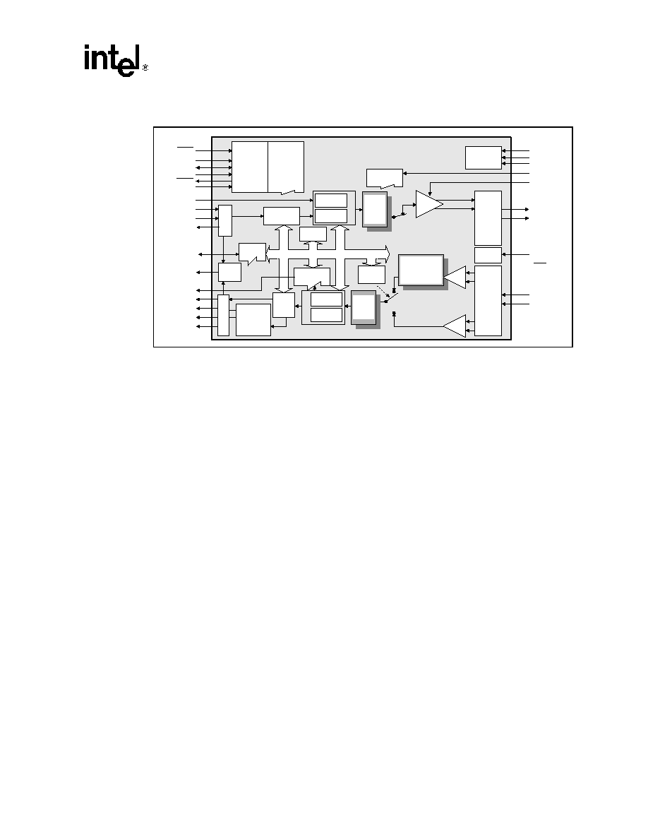
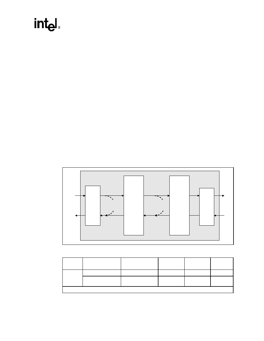
Figure 1. LXT972A Block Diagram
TX_EN
RX_ER
CRS
Pwr Supply
Management /
Mode Select
Logic
ADDR0
MDIO
MDC
MDINT
TX_ER
RXDV
TPON
TPOP
TPIN
TPIP
REFCLK
VCC
GND
COL
RX_CLK
TX_CLK
RESET
LED/CFG<3:1>
TXD<3:0>
Decoder &
Descrambler
+
-
Serial-to-
Parallel
Converter
Scrambler
& Encoder
Parallel/Serial
Converter
Carrier Sense
Data Valid
Error Detect
Auto
Negotiation
Manchester
Decoder
Manchester
Encoder
10
100
10
100
Media
Select
TP
Driver
TP Out
Register
Set
Register Set
Clock
Generator
+
-
10BT
Collision
Detect
Clock
Generator
TX
P
C
S
OSP
TM
Adaptive EQ with
Baseline Wander
Cancellation
OSP
TM
Slicer
OSP
TM
Pulse
Shaper
RXD<3:0>
+
-
100TX
TP In
MDDIS
TxSLEW<1:0>
RX
P
C
S
PWRDWN
JTAG
TDI,
TDO,
TMS,
TCK,
TRST
LXT972A 3.3 V Dual-Speed Fast Ethernet Transceiver
10
Datasheet
Document #: 249186
Revision #: 003
Rev. Date: August 7, 2002
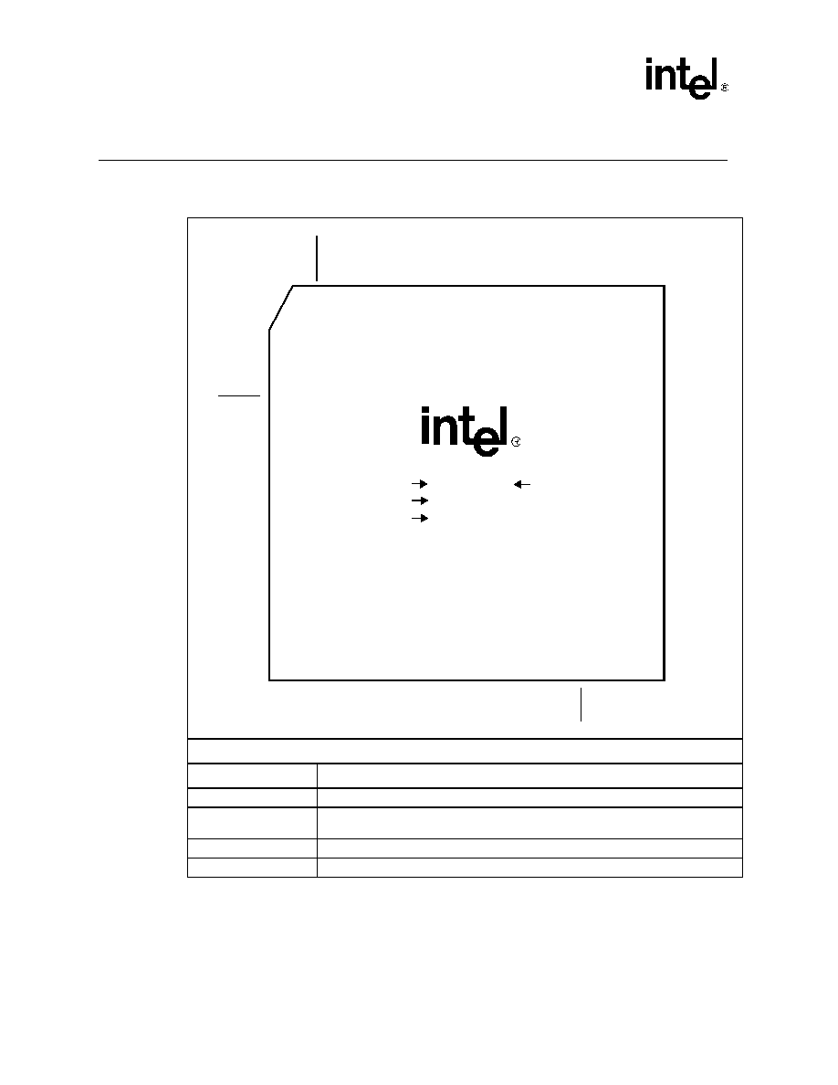
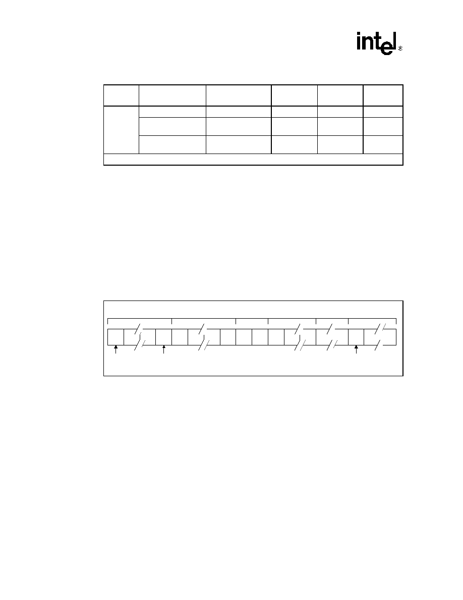
1.0
Pin Assignments
Figure 2. LXT972A 64-Pin LQFP Assignments
Package Topside Markings
Marking
Definition
Part #
LXT972A is the unique identifier for this product family.
Rev #
Identifies the particular silicon "stepping" (Refer to Specification Update for additional stepping
information.)
Lot #
Identifies the batch.
FPO #
Identifies the Finish Process Order.
RXD0
RBIAS
17
64
1
2
3
4
5
6
7
8
9
10
11
12
13
14
15
16
REFCLK/XI
XO
MDDIS
RESET
TXSLEW0
TXSLEW1
GND
VCCIO
N/C
N/C
GND
ADDR0
GND
GND
GND
GND
18
19
20
21
22
23
24
25
26
27
28
29
30
31
32
GND
TP
OP
TP
ON
VCCA
VCCA
TPI
P
TPI
N
GND
GND
TDI
TDO
TMS
TCK
TRS
T
GND
47
46
45
44
43
42
41
40
39
38
37
36
35
34
33
RXD1
RXD2
RXD3
N/C
MDC
MDIO
GND
VCCIO
PWRDWN
LED/CFG1
LED/CFG2
LED/CFG3
GND
GND
PAUSE
MDINT
CRS
COL
GND
TX
D3
TX
D2
TX
D1
TX
D0
TX
_EN
TX
_CL
K
TX
_ER
RX_ER
RX_CLK
VCCD
GND
RX_DV
63
62
61
60
59
58
57
56
55
54
53
52
51
50
49
48
LXT972A XX
XXXXXX
XXXXXXXX
Part #
LOT #
FPO #
Rev #

LXT972A 3.3 V Dual-Speed Fast Ethernet Transceiver
Datasheet
11
Document #: 249186
Revision #: 003
Rev. Date: August 7, 2002
Table 1. LQFP Numeric Pin List
Pin
Symbol
Type
Reference for
Full Description
1
REFCLK/XI
Input
Table 4 on page 14
2
XO
Output
Table 4 on page 14
3
MDDIS
Input
Table 2 on page 13
4
RESET Input
Table 4 on page 14
5
TxSLEW0
Input
Table 4 on page 14
6
TxSLEW1
Input
Table 4 on page 14
7
GND
≠
Table 5 on page 15
8
VCCIO
≠
Table 5 on page 15
9
N/C
≠
Table 4 on page 14
10
N/C
≠
Table 4 on page 14
11
GND
≠
Table 5 on page 15
12
ADDR0
Input
Table 4 on page 14
13
GND
≠
Table 5 on page 15
14
GND
≠
Table 5 on page 15
15
GND
≠
Table 5 on page 15
16
GND
≠
Table 5 on page 15
17
RBIAS
Analog Input
Table 4 on page 14
18
GND
≠
Table 5 on page 15
19
TPOP
Output
Table 3 on page 14
20
TPON
Output
Table 3 on page 14
21
VCCA
≠
Table 5 on page 15
22
VCCA
≠
Table 5 on page 15
23
TPIP
Input
Table 3 on page 14
24
TPIN
Input
Table 3 on page 14
25
GND
≠
Table 5 on page 15
26
GND
≠
Table 5 on page 15
27
TDI
Input
Table 6 on page 15
28
TDO
Output
Table 6 on page 15
29
TMS
Input
Table 6 on page 15
30
TCK
Input
Table 6 on page 15
31
TRST Input
Table 6 on page 15
32
GND
≠
Table 5 on page 15
33
PAUSE
Input
Table 4 on page 14
34
GND
≠
Table 4 on page 14
35
GND
≠
Table 4 on page 14
36
LED/CFG3
I/O
Table 7 on page 16

LXT972A 3.3 V Dual-Speed Fast Ethernet Transceiver
12
Datasheet
Document #: 249186
Revision #: 003
Rev. Date: August 7, 2002
37
LED/CFG2
I/O
Table 7 on page 16
38
LED/CFG1
I/O
Table 7 on page 16
39
PWRDWN
Input
Table 4 on page 14
40
VCCIO
≠
Table 5 on page 15
41
GND
≠
Table 5 on page 15
42
MDIO
I/O
Table 2 on page 13
43
MDC
Input
Table 2 on page 13
44
N/C
≠
Table 4 on page 14
45
RXD3
Output
Table 2 on page 13
46
RXD2
Output
Table 2 on page 13
47
RXD1
Output
Table 2 on page 13
48
RXD0
Output
Table 2 on page 13
49
RX_DV
Output
Table 2 on page 13
50
GND
≠
Table 5 on page 15
51
VCCD
≠
Table 5 on page 15
52
RX_CLK
Output
Table 2 on page 13
53
RX_ER
Output
Table 2 on page 13
54
TX_ER
Input
Table 2 on page 13
55
TX_CLK
Output
Table 2 on page 13
56
TX_EN
Input
Table 2 on page 13
57
TXD0
Input
Table 2 on page 13
58
TXD1
Input
Table 2 on page 13
59
TXD2
Input
Table 2 on page 13
60
TXD3
Input
Table 2 on page 13
61
GND
≠
Table 5 on page 15
62
COL
Output
Table 2 on page 13
63
CRS
Output
Table 2 on page 13
64
MDINT Open
Drain
Table 2 on page 13
Table 1. LQFP Numeric Pin List (Continued)
Pin
Symbol
Type
Reference for
Full Description
LXT972A 3.3 V Dual-Speed Fast Ethernet Transceiver
Datasheet
13
Document #: 249186
Revision #: 003
Rev. Date: August 7, 2002
2.0
Signal Descriptions
Intel recommends that all inputs and multi-function pins be tied to the inactive states and all
outputs be left floating, if unused.
Table 2. LXT972A MII Signal Descriptions
LQFP
Pin#
Symbol
Type
1
Signal Description
Data Interface Pins
60
59
58
57
TXD3
TXD2
TXD1
TXD0
I
Transmit Data. TXD is a bundle of parallel data signals that are driven by the
MAC. TXD<3:0> shall transition synchronously with respect to the TX_CLK.
TXD<0> is the least significant bit.
56
TX_EN
I
Transmit Enable. The MAC asserts this signal when it drives valid data on
TXD. This signal must be synchronized to TX_CLK.
55
TX_CLK
O
Transmit Clock. TX_CLK is sourced by the PHY in both 10 and 100 Mbps
operations. 2.5 MHz for 10 Mbps operation, 25 MHz for 100 Mbps operation.
45
46
47
48
RXD3
RXD2
RXD1
RXD0
O
Receive Data. RXD is a bundle of parallel signals that transition synchronously
with respect to the RX_CLK. RXD<0> is the least significant bit.
49
RX_DV
O
Receive Data Valid. The LXT972A asserts this signal when it drives valid data
on RXD. This output is synchronous to RX_CLK.
53
RX_ER
O
Receive Error. Signals a receive error condition has occurred. This output is
synchronous to RX_CLK.
54
TX_ER
I
Transmit Error. Signals a transmit error condition. This signal must be
synchronized to TX_CLK.
52
RX_CLK
O
Receive Clock. 25 MHz for 100 Mbps operation, 2.5 MHz for 10 Mbps
operation. Refer to
"Clock Requirements" on page 21
in the Functional
Description section.
62
COL
O
Collision Detected. The LXT972A asserts this output when a collision is
detected. This output remains High for the duration of the collision. This signal
is asynchronous and is inactive during full-duplex operation.
63
CRS
O
Carrier Sense. During half-duplex operation (bit 0.8 = 0), the LXT972A asserts
this output when either transmitting or receiving data packets. During full-
duplex operation (bit 0.8 = 1), CRS is asserted during receive. CRS assertion is
asynchronous with respect to RX_CLK. CRS is de-asserted on loss of carrier,
synchronous to RX_CLK.
MII Control Interface Pins
3
MDDIS
I
Management Disable. When MDDIS is High, the MDIO is disabled from read
and write operations.
When MDDIS is Low at power up or reset, the Hardware Control Interface pins
control only the initial or "default" values of their respective register bits. After
the power-up/reset cycle is complete, bit control reverts to the MDIO serial
channel.
1. Type Column Coding: I = Input, O = Output, A = Analog, OD = Open Drain.
LXT972A 3.3 V Dual-Speed Fast Ethernet Transceiver
14
Datasheet
Document #: 249186
Revision #: 003
Rev. Date: August 7, 2002
43
MDC
I
Management Data Clock. Clock for the MDIO serial data channel. Maximum
frequency is 8 MHz.
42
MDIO
I/O
Management Data Input/Output. Bidirectional serial data channel for PHY/
STA communication.
64
MDINT OD
Management Data Interrupt. When bit 18.1 = 1, an active Low output on this
pin indicates status change. Interrupt is cleared by reading Register 19.
Table 3.
LXT972A Network Interface Signal Descriptions
LQFP
Pin#
Symbol
Type
1
Signal Description
19
20
TPOP
TPON
O
Twisted-Pair Outputs, Positive & Negative.
During 100BASE-TX or 10BASE-T operation, TPOP/N pins drive 802.3
compliant pulses onto the line.
23
24
TPIP
TPIN
I
Twisted-Pair Inputs, Positive & Negative.
During 100BASE-TX or 10BASE-T operation, TPIP/N pins receive
differential 100BASE-TX or 10BASE-T signals from the line.
1. Type Column Coding: I = Input, O = Output, A = Analog, OD = Open Drain
Table 4.
LXT972A Miscellaneous Signal Descriptions
LQFP
Pin#
Symbol
Type
1
Signal Description
5
6
TxSLEW0
TxSLEW1
I
Tx Output Slew Controls 0 and 1. These pins select the TX output slew
rate (rise and fall time) as follows:
TxSLEW1
TxSLEW0
Slew Rate (Rise and Fall Time)
0
0
3.0 ns
0
1
3.4 ns
1
0
3.9 ns
1
1
4.4 ns
4
RESET
I
Reset. This active Low input is OR'ed with the control register Reset bit
(0.15). The LXT972A reset cycle is extended to 258
µs (nominal) after
reset is deasserted.
12
ADDR0
I
Address0. Sets device address.
17
RBIAS
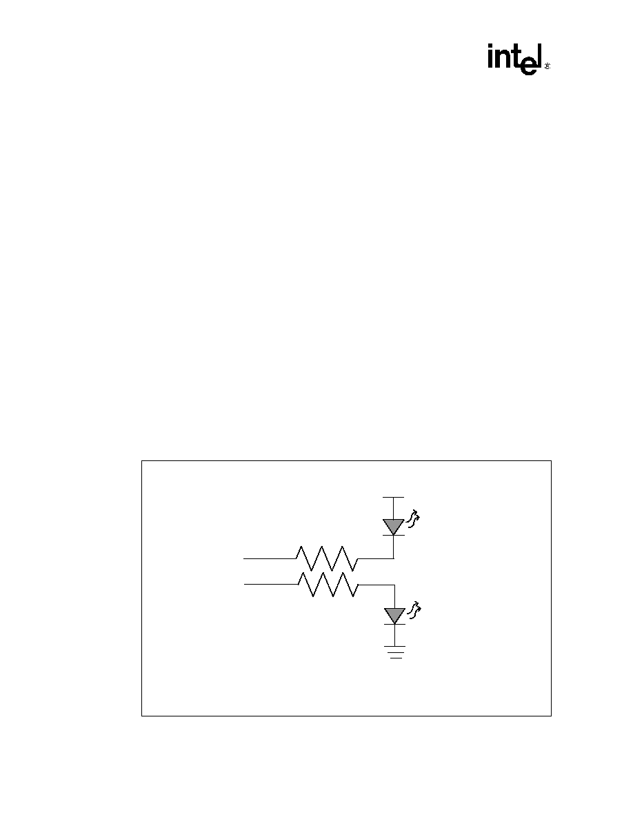
AI
Bias. This pin provides bias current for the internal circuitry. Must be tied
to ground through a 22.1 k
, 1% resistor.
33
PAUSE
I
Pause. When set High, the LXT972A advertises Pause capabilities during
auto negotiation.
1. Type Column Coding: I = Input, O = Output, A = Analog, OD = Open Drain
Table 2. LXT972A MII Signal Descriptions (Continued)
LQFP
Pin#
Symbol
Type
1
Signal Description
1. Type Column Coding: I = Input, O = Output, A = Analog, OD = Open Drain.
LXT972A 3.3 V Dual-Speed Fast Ethernet Transceiver
Datasheet
15
Document #: 249186
Revision #: 003
Rev. Date: August 7, 2002
39
PWRDWN
I
Power Down. When set High, this pin puts the LXT972A in a power-
down mode.
1
2
REFCLK/XI
XO
I
O
Crystal Input and Output. A 25 MHz crystal oscillator circuit can be
connected across XI and XO. A clock can also be used at XI. Refer to
Functional Description for detailed clock requirements.
9, 10,
44
N/C
-
No Connection. These pins are not used and should not be terminated.
Table 5. LXT972A Power Supply Signal Descriptions
LQFP
Pin#
Symbol
Type
Signal Description
51
VCCD
-
Digital Power. Requires a 3.3 V power supply.
7, 11, 13,
14, 15, 16,
18, 25, 26,
32, 34, 35,
41, 50, 61
GND
-
Ground.
8, 40
VCCIO
-
MII Power. Requires either a 3.3 V or a 2.5 V supply. Must be supplied
from the same source used to power the MAC on the other side of the MII.
21, 22
VCCA
-
Analog Power. Requires a 3.3 V power supply.
Table 6. LXT972A JTAG Test Signal Descriptions
LQFP
Pin#
Symbol
Type
1
Signal Description
27
TDI
2
I
Test Data Input. Test data sampled with respect to the rising edge of TCK.
28
TDO
2
O
Test Data Output. Test data driven with respect to the falling edge of TCK.
29
TMS
2
I
Test Mode Select.
30
TCK
2
I
Test Clock. Test clock input sourced by ATE.
31
TRST
2
I
Test Reset. Test reset input sourced by ATE.
1. Type Column Coding: I = Input, O = Output, A = Analog, OD = Open Drain.
2. If JTAG port is not used, these pins do not need to be terminated.
Table 7. LXT972A LED Signal Descriptions
LQFP
Pin#
Symbol
Type
1
Signal Description
38
37
36
LED/CFG1
LED/CFG2
LED/CFG3
I/O
LED Drivers 1 -3. These pins drive LED indicators. Each LED can
display one of several available status conditions as selected by the LED
Configuration Register (refer to
Table 52 on page 70
for details).
Configuration Inputs 1-3. These pins also provide initial configuration
settings (refer to
Table 9 on page 25
for details).
1. Type Column Coding: I = Input, O = Output, A = Analog, OD = Open Drain
Table 4. LXT972A Miscellaneous Signal Descriptions (Continued)
LQFP
Pin#
Symbol
Type
1
Signal Description
1. Type Column Coding: I = Input, O = Output, A = Analog, OD = Open Drain
LXT972A 3.3 V Dual-Speed Fast Ethernet Transceiver
16
Datasheet
Document #: 249186
Revision #: 003
Rev. Date: August 7, 2002
Table 8. LXT972A Pin Types and Modes
Modes
RXD 0-3
RXDV
Tx/Rx
CLKS
Output
RXER
Output
COL
Output
CRS
Output
TXD 0-3
Input
TXEN
Input
TXER
Input
HWReset
DL
DL
DH
DL
DL
DL IPLD
IPLD
IPLD
SFTPWRDN
DL
DL
Active
DL
DL
DL
IPLD
IPLD
IPLD
HWPWRDN
High Z
High Z
High Z
High Z
High Z
High Z
High Z
High Z
High Z
ISOLATE
HZ w/
IPLD
HZ w/
IPLD
HZ w/
IPLD
HZ w/
IPLD
HZ w/
IPLD
HZ w/
IPLD
IPLD
IPLD
IPLD
1. A High Z (High impedance) or three state determines when the device is drawing a current of less than
20 nA. A High Z with PLD (High impedance with pull-down) state determines when the device is drawing a
current of less than 20 uA.
2. DL = Driven Low (Logic 0), DH = Driven High (Logic 1), IPLD = Internal Pull-Down (Weak)

LXT972A 3.3 V Dual-Speed Fast Ethernet Transceiver
Datasheet
17
Document #: 249186
Revision #: 003
Rev. Date: August 7, 2002
3.0
Functional Description
3.1
Introduction
The LXT972A is a single-port Fast Ethernet 10/100 Transceiver that supports 10 Mbps and
100 Mbps networks. It complies with all applicable requirements of IEEE 802.3. The LXT972A
can directly drive either a 100BASE-TX line (up to 140 meters) or a 10BASE-T line (up to 185
meters).
3.1.1
Comprehensive Functionality
The LXT972A provides a standard Media Independent Interface (MII) for 10/100 MACs. The
LXT972A performs all functions of the Physical Coding Sublayer (PCS) and Physical Media
Attachment (PMA) sublayer as defined in the IEEE 802.3 100BASE-X standard. This device also
performs all functions of the Physical Media Dependent (PMD) sublayer for 100BASE-TX
connections.
On power-up, the LXT972A reads its configuration pins to check for forced operation settings. If
not configured for forced operation, it uses auto-negotiation/parallel detection to automatically
determine line operating conditions. If the PHY device on the other side of the link supports auto-
negotiation, the LXT972A auto-negotiates with it using Fast Link Pulse (FLP) Bursts. If the PHY
partner does not support auto-negotiation, the LXT972A automatically detects the presence of
either link pulses (10 Mbps PHY) or Idle symbols (100 Mbps PHY) and set its operating conditions
accordingly.
The LXT972A provides half-duplex and full-duplex operation at 100 Mbps and 10 Mbps.
3.1.2
OSPTM Architecture
Intel's LXT972A incorporates high-efficiency Optimal Signal ProcessingTM design techniques,
combining the best properties of digital and analog signal processing to produce a truly optimal
device.
The receiver utilizes decision feedback equalization to increase noise and cross-talk immunity by
as much as 3 dB over an ideal all-analog equalizer. Using OSP mixed-signal processing techniques
in the receive equalizer avoids the quantization noise and calculation truncation errors found in
traditional DSP-based receivers (typically complex DSP engines with A/D converters). This results
in improved receiver noise and cross-talk performance.
The OSP signal processing scheme also requires substantially less computational logic than
traditional DSP-based designs. This lowers power consumption and also reduces the logic
switching noise generated by DSP engines. This logic switching noise can be a considerable source
of EMI generated on the device's power supplies.
The OSP-based LXT972A provides improved data recovery, EMI performance and low power
consumption.

LXT972A 3.3 V Dual-Speed Fast Ethernet Transceiver
18
Datasheet
Document #: 249186
Revision #: 003
Rev. Date: August 7, 2002
3.2
Network Media / Protocol Support
The LXT972A supports both 10BASE-T and 100BASE-TX Ethernet over twisted-pair.
3.2.1
10/100 Network Interface
The network interface port consists of two differential signal pairs. Refer to
Table 3
for specific pin
assignments.
The LXT972A output drivers generate either 100BASE-TX or 10BASE-T. When not transmitting
data, the LXT972A generates 802.3-compliant link pulses or idle code. Input signals are decoded
either as a 100BASE-TX or 10BASE-T input, depending on the mode selected. Auto-negotiation/
parallel detection or manual control is used to determine the speed of this interface.
3.2.1.1
Twisted-Pair Interface
The LXT972A supports either 100BASE-TX or 10BASE-T connections over 100
, Category 5,
Unshielded Twisted Pair (UTP) cable. When operating at 100 Mbps, the LXT972A continuously
transmits and receives MLT3 symbols. When not transmitting data, the LXT972A generates
"IDLE" symbols.
During 10 Mbps operation, Manchester-encoded data is exchanged. When no data is being
exchanged, the line is left in an idle state. Link pulses are transmitted periodically to keep the link
up.
Only a transformer, RJ-45 connector, load resistor, and bypass capacitors are required to complete
this interface. On the transmit side, the LXT972A has an active internal termination and does not
require external termination resistors. Intel's patented waveshaping technology shapes the outgoing
signal to help reduce the need for external EMI filters. Four slew rate settings (refer to
Table 4 on
page 14
) allow the designer to match the output waveform to the magnetic characteristics. On the
receive side, the internal impedance is high enough that it has no practical effect on the external
termination circuit.
3.2.1.2
Fault Detection and Reporting
The LXT972A supports one fault detection and reporting mechanism. "Remote Fault" refers to a
MAC-to-MAC communication function that is essentially transparent to PHY layer devices. It is
used only during Auto-Negotiation, and therefore is applicable only to twisted-pair links. "Far-End
Fault" is an optional PMA-layer function that may be embedded within PHY devices. The
LXT972A supports only the Remote Fault Function, explained in the paragraph that follows.
Remote Fault
Register bit 4.13 in the Auto-Negotiation Advertisement Register is reserved for Remote Fault
indications. It is typically used when re-starting the auto-negotiation sequence to indicate to the
link partner that the link is down because the advertising device detected a fault.

LXT972A 3.3 V Dual-Speed Fast Ethernet Transceiver
Datasheet
19
Document #: 249186
Revision #: 003
Rev. Date: August 7, 2002
When the LXT972A receives a Remote Fault indication from its partner during auto-negotiation it
does the following:
∑
Sets Register bit 5.13 in the Link Partner Base Page Ability Register, and
∑
Sets the Remote Fault Register bit 1.4 in the MII Status Register to pass this information to the
local controller.
3.2.2
MII Data Interface
The LXT972A supports a standard Media Independent Interface (MII). The MII consists of a data
interface and a management interface. The MII Data Interface passes data between the LXT972A
and a Media Access Controller (MAC). Separate parallel buses are provided for transmit and
receive. This interface operates at either 10 Mbps or 100 Mbps. The speed is set automatically,
once the operating conditions of the network link have been determined. Refer to
"MII Operation"
on page 26
for additional details.
3.2.2.1
Increased MII Drive Strength
A higher Media Independent Interface (MII) drive strength may be desired in some designs to drive
signals over longer PCB trace lengths, or over high-capacitive loads, through multiple vias, or
through a connector. The MII drive strength in the LXT971A can be increased by setting Register
bit 26.11 through software control. Setting Register bit 26.11 = 1 through the MDC/MDIO
interface sets the MII pins (RXD[0:3], RX_DV, RX_CLK, RX_ER, COL, CRS, and TX_CLK) to a
higher drive strength.
3.2.3
Configuration Management Interface
The LXT972A provides both an MDIO interface and a Hardware Control Interface for device
configuration and management.
3.2.3.1
MDIO Management Interface
The LXT972A supports the IEEE 802.3 MII Management Interface also known as the
Management Data Input/Output (MDIO) Interface. This interface allows upper-layer devices to
monitor and control the state of the LXT972A. The MDIO interface consists of a physical
connection, a specific protocol that runs across the connection, and an internal set of addressable
registers.
Some registers are required and their functions are defined by the IEEE 802.3 standard. The
LXT972A also supports additional registers for expanded functionality. The LXT972A supports
multiple internal registers, each of which is 16 bits wide. Specific register bits are referenced using
an "X.Y" notation, where X is the register number (0-31) and Y is the bit number (0-15).
The physical interface consists of a data line (MDIO) and clock line (MDC). Operation of this
interface is controlled by the MDDIS input pin. When MDDIS is High, the MDIO read and write
operations are disabled and the Hardware Control Interface provides primary configuration control.
When MDDIS is Low, the MDIO port is enabled for both read and write operations and the
Hardware Control Interface is not used.
LXT972A 3.3 V Dual-Speed Fast Ethernet Transceiver
20
Datasheet
Document #: 249186
Revision #: 003
Rev. Date: August 7, 2002
MDIO Addressing
The protocol allows one controller to communicate between two LXT972A chips. Pin ADDR0 is
set high or low to determine the chip address.
MDIO Frame Structure
The physical interface consists of a data line (MDIO) and clock line (MDC). The frame structure is
shown in
Figure 3
and
Figure 4
(read and write). MDIO Interface timing is shown in
Table 34 on
page 55
.
3.2.3.2
MII Interrupts
The LXT972A provides a single interrupt pin (MDINT). Interrupt logic is shown in
Figure 5
. The
LXT972A also provides two dedicated interrupt registers. Register 18 provides interrupt enable
and mask functions and Register 19 provides interrupt status. Setting bit 18.1 = 1, enables the
device to request interrupt via the MDINT pin. An active Low on this pin indicates a status change
on the LXT972A. Interrupts may be caused by four conditions:
∑
Auto-negotiation complete
∑
Speed status change
∑
Duplex status change
∑
Link status change
3.2.3.3
Hardware Control Interface
The LXT972A provides a Hardware Control Interface for applications where the MDIO is not
desired. The Hardware Control Interface uses the three LED driver pins to set device configuration.
Refer to
Section 3.4.5, "Hardware Configuration Settings" on page 24
for additional details.
Figure 3. Management Interface Read Frame Structure
Figure 4. Management Interface Write Frame Structure
MDC
MDIO
(Read)
32 "1"s
0
1
1
0
Preamble
ST
Op Code
PHY Address
Turn
Around
Z
0
A4
A3
A0
R4
R3
R0
Register Address
D15
D14
D1
Data
Write
Read
D15
D14
D1
D0
Idle
High Z
MDC
MDIO
(Write)
32 "1"s
0
1
0
1
Preamble
ST
Op Code
PHY Address
Turn
Around
1
0
A4
A3
A0
R4
R3
R0
Register Address
D15
D14
D1
D0
Data
Idle
Idle
Write
LXT972A 3.3 V Dual-Speed Fast Ethernet Transceiver
Datasheet
21
Document #: 249186
Revision #: 003
Rev. Date: August 7, 2002
3.3
Operating Requirements
3.3.1
Power Requirements
The LXT972A requires three power supply inputs (VCCD, VCCA, and VCCIO). The digital and
analog circuits require 3.3 V supplies (VCCD and VCCA). These inputs may be supplied from a
single source. Each supply input must be decoupled to ground.
An additional supply may be used for the MII (VCCIO). The supply may be either +2.5 V or
+3.3 V. The inputs on the MII interface are tolerant to 5 V signals from the controller on the other
side of the MII interface. Refer to
Table 20 on page 46
for MII I/O characteristics.
As a matter of good practice, these supplies should be as clean as possible.
3.3.2
Clock Requirements
3.3.2.1
External Crystal/Oscillator
The LXT972A requires a reference clock input that is used to generate transmit signals and recover
receive signals. It may be provided by either of two methods: by connecting a crystal across the
oscillator pins (XI and XO), or by connecting an external clock source to pin XI. The connection of
a clock source to the XI pin requires the XO pin to be left open. A crystal-based clock is
recommended over a derived clock (i.e., PLL-based) to minimize transmit jitter. Refer to the
LXT971A/972A Design and Layout Guide for a list of recommended clock sources.
A crystal is typically used in NIC applications. An external 25 MHz clock source, rather than a
crystal, is frequently used in switch applications. Refer to
Table 21 on page 46
for clock timing
requirements
3.3.2.2
MDIO Clock
The MII management channel (MDIO) also requires an external clock. The managed data clock
(MDC) speed is a maximum of 8 MHz. Refer to
Table 34 on page 55
for details.
Figure 5. Interrupt Logic
Force Interrupt
Interrupt Enable
Event X Mask Reg
Event X Status Reg
Interrupt Pin
.
.
.
AND
OR
NAND
Per Event
1. Interrupt (Event) Status Register is cleared on read.
(MDINT)

LXT972A 3.3 V Dual-Speed Fast Ethernet Transceiver
22
Datasheet
Document #: 249186
Revision #: 003
Rev. Date: August 7, 2002
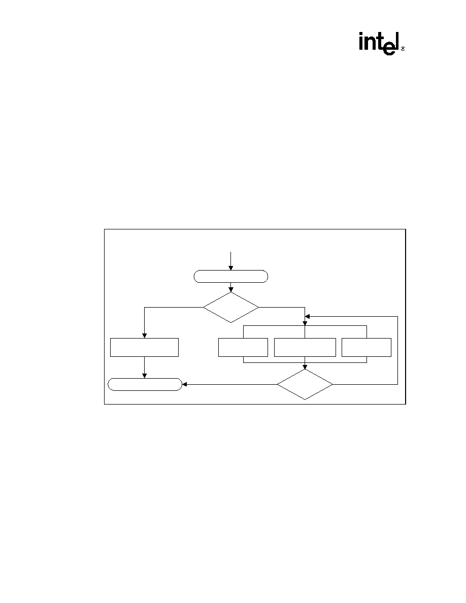
3.4
Initialization
When the LXT972A is first powered on, reset, or encounters a link failure state, it checks the
MDIO register configuration bits to determine the line speed and operating conditions to use for
the network link. The configuration bits may be set by the Hardware Control or MDIO interface as
shown in
Figure 6
.
3.4.1
MDIO Control Mode
In the MDIO Control mode, the LXT972A reads the Hardware Control Interface pins to set the
initial (default) values of the MDIO registers. Once the initial values are set, bit control reverts to
the MDIO interface.
3.4.2
Hardware Control Mode
In the Hardware Control Mode, LXT972A disables direct write operations to the MDIO registers
via the MDIO Interface. On power-up or hardware reset the LXT972A reads the Hardware Control
Interface pins and sets the MDIO registers accordingly.
The following modes are available using either Hardware Control or MDIO Control:
∑
Force network link operation to:
100BASE-TX, Full-Duplex
100BASE-TX, Half-Duplex
10BASE-T, Full-Duplex
10BASE-T, Half-Duplex
∑
Allow auto-negotiation/parallel-detection
When the network link is forced to a specific configuration, the LXT972A immediately begins
operating the network interface as commanded. When auto-negotiation is enabled, the LXT972A
begins the auto-negotiation/parallel-detection operation.
LXT972A 3.3 V Dual-Speed Fast Ethernet Transceiver
Datasheet
23
Document #: 249186
Revision #: 003
Rev. Date: August 7, 2002
3.4.3
Reduced Power Modes
The LXT972A offers two power-down modes.
3.4.3.1
Hardware Power Down
The hardware power-down mode is controlled by the PWRDWN pin. When PWRDWN is High,
the following conditions are true:
∑
The LXT972A network port and clock are shut down.
∑
All outputs are three-stated.
∑
All weak pad pull-up and pull-down resistors are disabled.
∑
The MDIO registers are not accessible.
Figure 6. Initialization Sequence
MDDIS Voltage
Level?
High
Low
MDIO Control
Mode
Hardware Control
Mode
Disable MDIO Read and
Write Operations
Reset MDIO Registers to
values read at H/W
Control Interface at last
Hardware Reset
MDIO Controlled Operation
(MDIO Writes Enabled)
Power-up or Reset
Initialize MDIO Registers
Read H/W Control
Interface
Software
Reset?
Yes
No
LXT972A 3.3 V Dual-Speed Fast Ethernet Transceiver
24
Datasheet
Document #: 249186
Revision #: 003
Rev. Date: August 7, 2002
3.4.3.2
Software Power Down
Software power-down control is provided by bit 0.11 in the Control Register (refer to
Table 39 on
page 60
). During soft power-down, the following conditions are true:
∑
The network port is shut down.
∑
The MDIO registers remain accessible.
3.4.4
Reset
The LXT972A provides both hardware and software resets. Configuration control of auto-
negotiation, speed, and duplex mode selection is handled differently for each. During a hardware
reset, auto-negotiation and speed are read in from pins (refer to
Table 9 on page 25
for pin settings
and to
Table 39 on page 60
for register bit definitions).
During a software reset (0.15 = 1), these bit settings are not re-read from the pins. They revert back
to the values that were read in during the last hardware reset. Therefore, any changes to pin values
made since the last hardware reset are not detected during a software reset.
During a hardware reset, register information is unavailable for 1 ms after de-assertion of the reset.
During a software reset (0.15 = 1) the registers are available for reading. The reset bit should be
polled to see when the part has completed reset (0.15 = 0).
3.4.5
Hardware Configuration Settings
The LXT972A provides a hardware option to set the initial device configuration. The hardware
option uses the three LED driver pins. This provides three control bits, as listed in
Table 9
. The
LED drivers can operate as either open-drain or open-source circuits as shown in
Figure 7
.
.
Figure 7. Hardware Configuration Settings
Configuration Bit = 1
Configuration Bit = 0
LED/CFG Pin
LED/CFG Pin
3.3 V
1. The LED/CFG pins automatically adjust their
polarity upon power-up or reset.
2. Unused LEDs may be implemented with pull-up/
pull-down resistors of 10 K.

LXT972A 3.3 V Dual-Speed Fast Ethernet Transceiver
Datasheet
25
Document #: 249186
Revision #: 003
Rev. Date: August 7, 2002
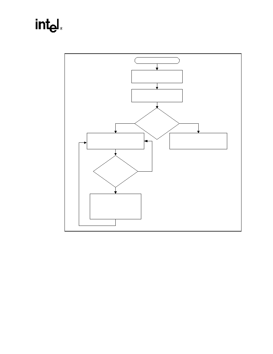
3.5
Establishing Link
See
Figure 8
for an overview of link establishment.
3.5.1
Auto-Negotiation
If not configured for forced operation, the LXT972A attempts to auto-negotiate with its link
partner by sending Fast Link Pulse (FLP) bursts. Each burst consists of up to 33 link pulses spaced
62.5
µs apart. Odd link pulses (clock pulses) are always present. Even link pulses (data pulses) may
be present or absent to indicate a "1" or a "0". Each FLP burst exchanges 16 bits of data, which are
referred to as a "link code word". All devices that support auto-negotiation must implement the
"Base Page" defined by IEEE 802.3 (registers 4 and 5). LXT972A also supports the optional "Next
Page" function as described in
Table 46
and
Table 47
(registers 7 and 8).
3.5.1.1
Base Page Exchange
By exchanging Base Pages, the LXT972A and its link partner communicate their capabilities to
each other. Both sides must receive at least three identical base pages for negotiation to continue.
Each side identifies the highest common capabilities that both sides support and configures itself
accordingly.
3.5.1.2
Next Page Exchange
Additional information, above that required by base page exchange, is also sent via "Next Pages".
The LXT972A fully supports the IEEE 802.3ab method of negotiation via Next Page exchange.
Table 9. Hardware Configuration Settings
Desired Mode
LED/CFGn
Pin Settings
1
Resulting Register Bit Values
Control Register
Auto-Neg Advertisement
Auto-Neg
Speed
(Mbps)
Duplex
1
2
3
AutoNeg
0.12
Speed
0.13
FD
0.8
100FD
4.8
100TX
4.7
10FD
4.6
10T
4.5
Disabled
10
Half
Low
Low
Low
0
0
0
N/A
Auto-Negotiation Advertisement
Full
Low
Low
High
1
100
Half
Low
High
Low
1
0
Full
Low
High
High
1
Enabled
100 Only
Half
High
Low
Low
1
1
0
0
1
0
0
Full
High
Low
High
1
1
1
0
0
10/100
Half Only
High
High
Low
0
0
1
0
1
Full or
Half
High
High
High
1
1
1
1
1
1. Refer to
Table 7 on page 16
for LED/CFG pin assignments.
LXT972A 3.3 V Dual-Speed Fast Ethernet Transceiver
26
Datasheet
Document #: 249186
Revision #: 003
Rev. Date: August 7, 2002
3.5.1.3
Controlling Auto-Negotiation
When auto-negotiation is controlled by software, the following steps are recommended:
∑
After power-up, power-down, or reset, the power-down recovery time, as specified in
Table 36
on page 56
, must be exhausted before proceeding.
∑
Set the Auto-Negotiation Advertise Register bits.
∑
Enable auto-negotiation (set MDIO Register bit 0.12 = 1).
3.5.2
Parallel Detection
For the parallel detection feature of auto-negotiation, the LXT972A also monitors for 10BASE-T
Normal Link Pulses (NLP) and 100BASE-TX Idle symbols. If either is detected, the device
automatically reverts to the corresponding operating mode. Parallel detection allows the LXT972A
to communicate with devices that do not support auto-negotiation.
3.6
MII Operation
The LXT972A device implements the Media Independent Interface (MII) as defined in the IEEE
802.3 standard. Separate channels are provided for transmitting data from the MAC to the
LXT972A (TXD), and for passing data received from the line (RXD) to the MAC. Each channel
has its own clock, data bus, and control signals. Nine signals are used to pass received data to the
MAC: RXD<3:0>, RX_CLK, RX_DV, RX_ER, COL, and CRS. Seven signals are used to transmit
data from the MAC: TXD<3:0>, TX_CLK, TX_EN, and TX_ER.
The LXT972A supplies both clock signals as well as separate outputs for carrier sense and
collision. Data transmission across the MII is normally implemented in 4-bit-wide nibbles.
Figure 8. Link Establishment Overview
Check Value
0.12
Start
Done
Enable
Auto-Neg/Parallel Detection
Go To Forced
Settings
Attempt Auto-
Negotiation
Listen for 10T
Link Pulses
Listen for 100TX
Idle Symbols
Link Up?
NO
YES
Power-Up, Reset,
or Link Failure
Disable
Auto-Negotiation
0.12 = 0
0.12 = 1

LXT972A 3.3 V Dual-Speed Fast Ethernet Transceiver
Datasheet
27
Document #: 249186
Revision #: 003
Rev. Date: August 7, 2002
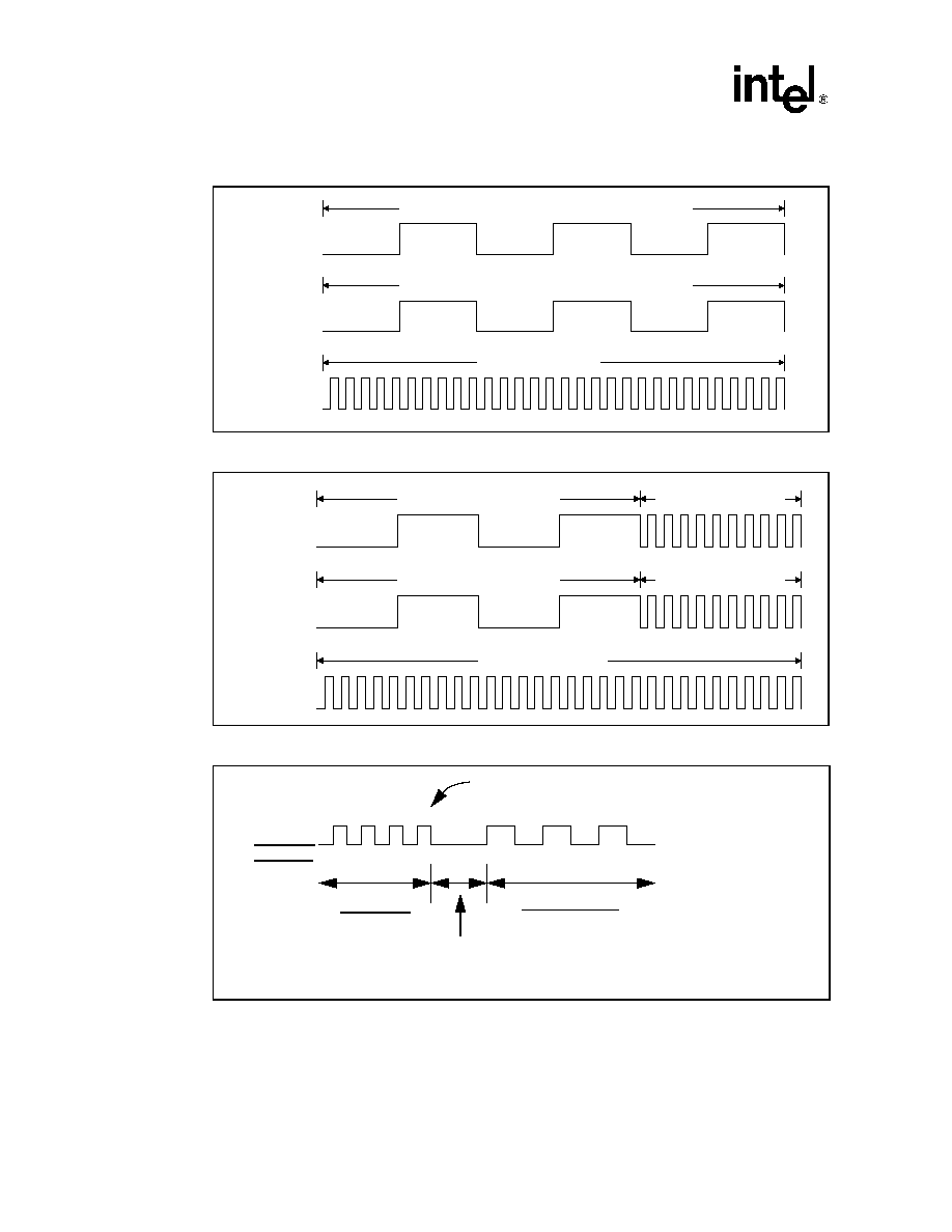
3.6.1
MII Clocks
The LXT972A is the master clock source for data transmission and supplies both MII clocks
(RX_CLK and TX_CLK). It automatically sets the clock speeds to match link conditions. When
the link is operating at 100 Mbps, the clocks are set to 25 MHz. When the link is operating at
10 Mbps, the clocks are set to 2.5 MHz.
Figure 9
through
Figure 11
show the clock cycles for each
mode. The transmit data and control signals must always be synchronized to TX_CLK by the
MAC. The LXT972A samples these signals on the rising edge of TX_CLK.
3.6.2
Transmit Enable
The MAC must assert TX_EN the same time as the first nibble of preamble, and de-assert TX_EN
after the last bit of the packet.
3.6.3
Receive Data Valid
The LXT972A asserts RX_DV when it receives a valid packet. Timing changes depend on line
operating speed:
∑
For 100TX links, RX_DV is asserted from the first nibble of preamble to the last nibble of the
data packet.
∑
For 10BT links, the entire preamble is truncated. RX_DV is asserted with the first nibble of the
Start of Frame Delimiter (SFD) "5D" and remains asserted until the end of the packet.
3.6.4
Carrier Sense
Carrier sense (CRS) is an asynchronous output. It is always generated when a packet is received
from the line and in half-duplex when a packet is transmitted.
Carrier sense is not generated when a packet is transmitted and in full-duplex mode.
Table 10
summarizes the conditions for assertion of carrier sense, collision, and data loopback signals.
3.6.5
Error Signals
When LXT972A is in 100 Mbps mode and receives an invalid symbol from the network, it asserts
RX_ER and drives "1110" on the RXD pins.
When the MAC asserts TX_ER, the LXT972A drives "H" symbols out on the TPOP/N pins.
3.6.6
Collision
The LXT972A asserts its collision signal, asynchronously to any clock, whenever the line state is
half-duplex and the transmitter and receiver are active at the same time.
Table 10
summarizes the
conditions for assertion of carrier sense, collision, and data loopback signals.
LXT972A 3.3 V Dual-Speed Fast Ethernet Transceiver
28
Datasheet
Document #: 249186
Revision #: 003
Rev. Date: August 7, 2002
Figure 9. 10BASE-T Clocking
Figure 10. 100BASE-X Clocking
Figure 11. Link Down Clock Transition
RX_CLK
(Sourced by LXT972A)
2.5 MHz during auto-negotiation and 10BASE-T Data & Idle
TX_CLK
(Sourced by LXT972A)
2.5 MHz during auto-negotiation and 10BASE-T Data & Idle
Constant 25 MHz
XI
RX_CLK
(Sourced by LXT972A)
2.5 MHz during auto-negotiation
TX_CLK
(Sourced by LXT972A)
Constant 25 MHz
XI
25 MHz once 100BASE-X
Link Established
2.5 MHz during auto-negotiation
25 MHz once 100BASE-X
Link Established
Any Clock
2.5MHz Clock
Clock transition time will not exceed 2X the
Link Down condition/Auto Negotiate Enabled
RX_CLK
TX_CLK
nominal clock period: (10 Mbps = 2.5 MHz;
100 Mbps = 25 MHz)
LXT972A 3.3 V Dual-Speed Fast Ethernet Transceiver
Datasheet
29
Document #: 249186
Revision #: 003
Rev. Date: August 7, 2002
3.6.7
Loopback
The LXT972A provides two loopback functions, operational and test (see
Table 10
). Loopback
paths are shown in
Figure 12
.
3.6.7.1
Operational Loopback
Operational loopback is provided for 10 Mbps half-duplex links when bit 16.8 = 0. Data
transmitted by the MAC (TXData) is looped back on the receive side of the MII (RXData).
Operational loopback is not provided for 100 Mbps links, full-duplex links, or when 16.8 = 1.
3.6.7.2
Test Loopback
A test loopback function is provided for diagnostic testing of the LXT972A. During test loopback,
the twisted-pair interface is disabled. Data transmitted by the MAC is internally looped back by the
LXT972A and returned to the MAC.
Test loopback is available for both 100TX and 10T operation. Test loopback is enabled by setting
bits as follows:
∑
0.14 = 1
∑
0.8 = 1 (full-duplex)
∑
0.12 = 0 (disable auto-negotiation).
Figure 12. Loopback Paths
Table 10. Carrier Sense, Loopback, and Collision Conditions
Speed
Duplex Condition
Carrier Sense
Test
1
Loopback
Operational
Loopback
Collision
100 Mbps
Full-Duplex
Receive Only
Yes
No
None
Half-Duplex
Transmit or Receive
No
No
Transmit and
Receive
1. Test Loopback is enabled when Register bit 0.14 = 1
10T
Loopback
Digital
Block
MII
TX Driver
100X
Loopback
Analog
Block
LXT972A
LXT972A 3.3 V Dual-Speed Fast Ethernet Transceiver
30
Datasheet
Document #: 249186
Revision #: 003
Rev. Date: August 7, 2002
3.7
100 Mbps Operation
3.7.1
100BASE-X Network Operations
During 100BASE-X operation, the LXT972A transmits and receives 5-bit symbols across the
network link.
Figure 13
shows the structure of a standard frame packet. When the MAC is not
actively transmitting data, the LXT972A sends out Idle symbols on the line.
In 100TX mode, the LXT972A scrambles and transmits the data to the network using MLT-3 line
code (
Figure 14 on page 31
). MLT-3 signals received from the network are descrambled, decoded,
and sent across the MII to the MAC.
10 Mbps
Full-Duplex
Receive Only
Yes
No
None
Half-Duplex,
Register bit 16.8 = 0
Transmit or Receive
Yes
Yes
Transmit and
Receive
Half-Duplex,
Register bit 16.8 = 1
Transmit or Receive
No
No
Transmit and
Receive
Table 10. Carrier Sense, Loopback, and Collision Conditions (Continued)
Speed
Duplex Condition
Carrier Sense
Test
1
Loopback
Operational
Loopback
Collision
1. Test Loopback is enabled when Register bit 0.14 = 1
Figure 13. 100BASE-X Frame Format
P0
P1
P6
SFD
64-Bit Preamble
(8 Octets)
Start-of-Frame
Delimiter (SFD)
DA
DA
SA
SA
Destination and Source
Address (6 Octets each)
L1
L2
Packet Length
(2 Octets)
D0
D1
Dn
Data Field
(Pad to minimum packet size)
Frame Check Field
(4 Octets)
CRC
I0
InterFrame Gap / Idle Code
(> 12 Octets)
Replaced by
/T/R/ code-groups
End-of-Stream Delimiter (ESD)
IFG
Replaced by
/J/K/ code-groups
Start-of-Stream
Delimiter (SSD)
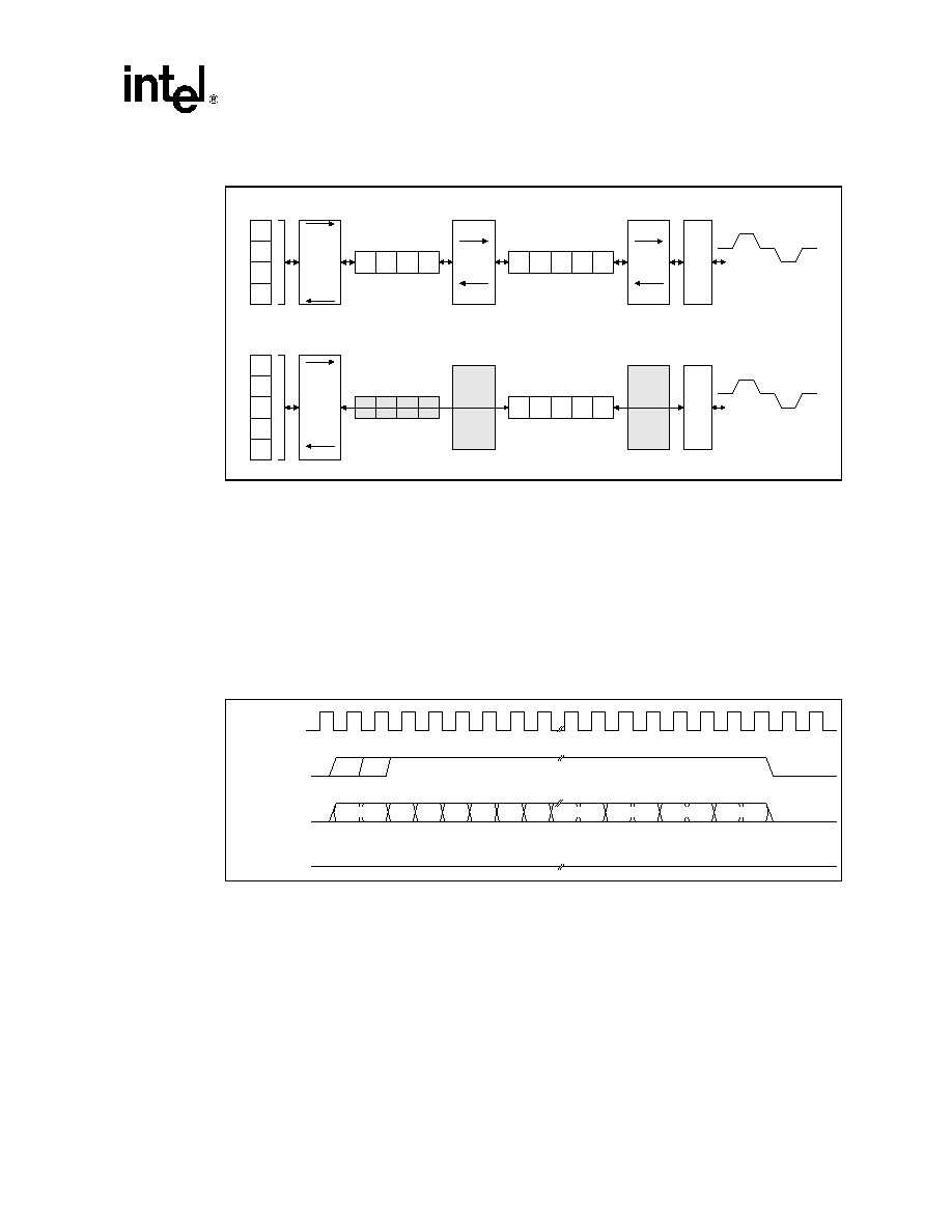
LXT972A 3.3 V Dual-Speed Fast Ethernet Transceiver
Datasheet
31
Document #: 249186
Revision #: 003
Rev. Date: August 7, 2002
.
As shown in
Figure 13 on page 30
, the MAC starts each transmission with a preamble pattern. As
soon as the LXT972A detects the start of preamble, it transmits a Start-of-Stream Delimiter (SSD,
symbols J and K) to the network. It then encodes and transmits the rest of the packet, including the
balance of the preamble, the SFD, packet data, and CRC.
Once the packet ends, the LXT972A transmits the End-of Stream-Delimiter (ESD, symbols T and
R) and then returns to transmitting Idle symbols. 4B/5B coding is shown in
Table 11 on page 34
.
Figure 15
shows normal reception with no errors. When the LXT972A receives invalid symbols
from the line, it asserts RX_ER as shown in
Figure 16
.
Figure 14. 100BASE-TX Data Path
S0
S1
S2
S3
S4
Parallel
to
Serial
Serial
to
Parallel
MLT3
0
+1
-1
0
0
Transition = 1.
No Transition = 0.
All transitions must follow
pattern: 0, +1, 0, -1, 0, +1...
Scrambler Bypass Data Flow
S0 S1 S2 S3 S4
Standard Data Flow
D0
D1
D2
D3
Parallel
to
Serial
Serial
to
Parallel
D0 D1 D2 D3
4B/5B
S0 S1 S2 S3 S4
MLT3
0
+1
-1
0
0
Transition = 1.
No Transition = 0.
All transitions must follow
pattern: 0, +1, 0, -1, 0, +1...
Scramble
De-
Scramble
Figure 15. 100BASE-TX Reception with no Errors
RX_CLK
RX_DV
RXD<3:0>
RX_ER
preamble SFD SFD DA
DA
DA
DA
CRC
CRC
CRC
CRC
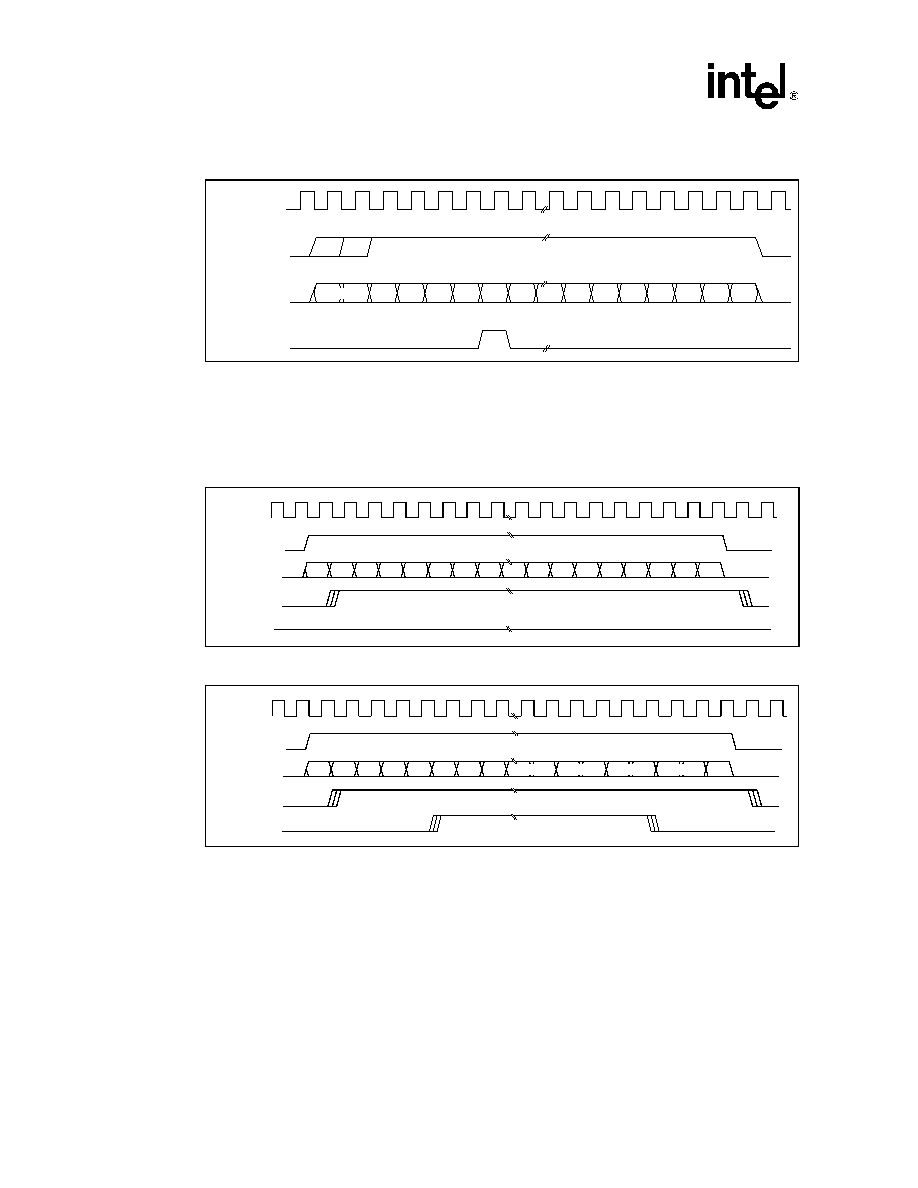
LXT972A 3.3 V Dual-Speed Fast Ethernet Transceiver
32
Datasheet
Document #: 249186
Revision #: 003
Rev. Date: August 7, 2002
3.7.2
Collision Indication
Figure 17
shows normal transmission. Upon detection of a collision, the COL output is asserted
and remains asserted for the duration of the collision as shown in
Figure 18
.
3.7.3
100BASE-X Protocol Sublayer Operations
With respect to the 7-layer communications model, the LXT972A is a Physical Layer 1 (PHY)
device. The LXT972A implements the Physical Coding Sublayer (PCS), Physical Medium
Attachment (PMA), and Physical Medium Dependent (PMD) sublayers of the reference model
defined by the IEEE 802.3u standard. The following paragraphs discuss LXT972A operation from
the reference model point of view.
Figure 16. 100BASE-TX Reception with Invalid Symbol
RX_CLK
RX_DV
RXD<3:0>
RX_ER
preamble SFD SFD DA
DA
XX
XX
XX
XX
XX
XX
XX
XX
XX
XX
Figure 17. 100BASE-TX Transmission with no Errors
Figure 18. 100BASE-TX Transmission with Collision
DA DA DA DA DA
DA
DA
DA DA
TX_CLK
TX_EN
TXD<3:0>
CRS
COL
P
R
E
A
M
B
L
E
JAM
TX_CLK
TX_EN
TXD<3:0>
CRS
COL
P
R
E
A
M
B
L
E
JAM
JAM
JAM
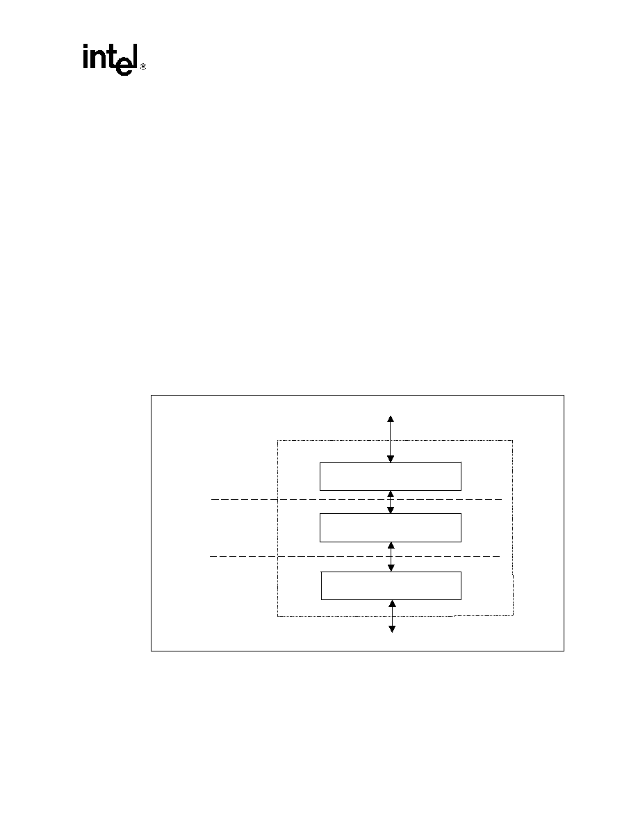
LXT972A 3.3 V Dual-Speed Fast Ethernet Transceiver
Datasheet
33
Document #: 249186
Revision #: 003
Rev. Date: August 7, 2002
3.7.3.1
PCS Sublayer
The Physical Coding Sublayer (PCS) provides the MII interface, as well as the 4B/5B encoding/
decoding function.
For 100BASE-TX operation, the PCS layer provides IDLE symbols to the PMD-layer line driver
as long as TX_EN is de-asserted.
Preamble Handling
When the MAC asserts TX_EN, the PCS substitutes a /J/K symbol pair, also known as the Start-of-
Stream Delimiter (SSD), for the first two nibbles received across the MII. The PCS layer continues
to encode the remaining MII data, following the coding in
Table 11 on page 34
, until TX_EN is de-
asserted. It then returns to supplying IDLE symbols to the line driver.
In the receive direction, the PCS layer performs the opposite function, substituting two preamble
nibbles for the SSD.
Dribble Bits
The LXT972A handles dribbles bits in all modes. If between one through four dribble bits are
received, the nibble is passed across the MII, padded with 1s if necessary. If between five through
seven dribble bits are received, the second nibble is not sent onto the MII bus.
Figure 19. Protocol Sublayers
Encoder/Decoder
Serializer/De-serializer
Link/Carrier Detect
PCS
Sublayer
PMA
Sublayer
MII Interface
LXT972A
100BASE-TX
Scrambler/
De-scrambler
PMD
Sublayer

LXT972A 3.3 V Dual-Speed Fast Ethernet Transceiver
34
Datasheet
Document #: 249186
Revision #: 003
Rev. Date: August 7, 2002
Table 11. 4B/5B Coding
Code Type
4B Code
3 2 1 0
Name
5B Code
4 3 2 1 0
Interpretation
0 0 0 0
0
1 1 1 1 0
Data 0
0 0 0 1
1
0 1 0 0 1
Data 1
0 0 1 0
2
1 0 1 0 0
Data 2
0 0 1 1
3
1 0 1 0 1
Data 3
0 1 0 0
4
0 1 0 1 0
Data 4
0 1 0 1
5
0 1 0 1 1
Data 5
0 1 1 0
6
0 1 1 1 0
Data 6
DATA
0 1 1 1
7
0 1 1 1 1
Data 7
1 0 0 0
8
1 0 0 1 0
Data 8
1 0 0 1
9
1 0 0 1 1
Data 9
1 0 1 0
A
1 0 1 1 0
Data A
1 0 1 1
B
1 0 1 1 1
Data B
1 1 0 0
C
1 1 0 1 0
Data C
1 1 0 1
D
1 1 0 1 1
Data D
1 1 1 0
E
1 1 1 0 0
Data E
1 1 1 1
F
1 1 1 0 1
Data F
IDLE
undefined
I
1
1 1 1 11
Idle. Used as inter-stream fill code
0 1 0 1
J
2
1 1 0 0 0
Start-of-Stream Delimiter (SSD), part 1
of 2
CONTROL
0 1 0 1
K
2
1 0 0 0 1
Start-of-Stream Delimiter (SSD), part 2
of 2
undefined
T
3
0 1 1 0 1
End-of-Stream Delimiter (ESD), part 1
of 2
undefined
R
3
0 0 1 1 1
End-of-Stream Delimiter (ESD), part 2
of 2
undefined
H
4
0 0 1 0 0
Transmit Error. Used to force signaling
errors
undefined
Invalid
0 0 0 0 0
Invalid
undefined
Invalid
0 0 0 0 1
Invalid
undefined
Invalid
0 0 0 1 0
Invalid
INVALID
undefined
Invalid
0 0 0 1 1
Invalid
undefined
Invalid
0 0 1 0 1
Invalid
undefined
Invalid
0 0 1 1 0
Invalid
undefined
Invalid
0 1 0 0 0
Invalid
1. The /I/ (Idle) code group is sent continuously between frames.
2. The /J/ and /K/ (SSD) code groups are always sent in pairs; /K/ follows /J/.
3. The /T/ and /R/ (ESD) code groups are always sent in pairs; /R/ follows /T/.
4. An /H/ (Error) code group is used to signal an error condition.
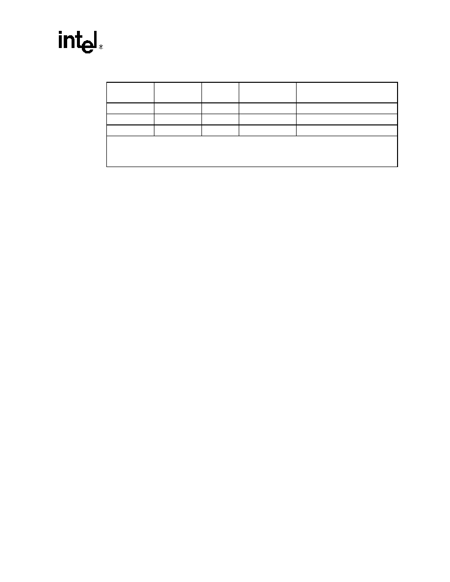
LXT972A 3.3 V Dual-Speed Fast Ethernet Transceiver
Datasheet
35
Document #: 249186
Revision #: 003
Rev. Date: August 7, 2002
3.7.3.2
PMA Sublayer
Link
In 100 Mbps mode, the LXT972A establishes a link whenever the scrambler becomes locked and
remains locked for approximately 50 ms. Whenever the scrambler loses lock (receiving less than
12 consecutive idle symbols during a 2 ms window), the link are taken down. This provides a very
robust link, essentially filtering out any small noise hits that may otherwise disrupt the link.
Furthermore, 100 M idle patterns will not bring up a 10 Mbps link.
The LXT972A reports link failure via the MII status bits Register bits 1.2 and 17.10) and interrupt
functions. If auto-negotiation is enabled, link failure causes the LXT972A to re-negotiate.
Link Failure Override
The LXT972A normally transmits data packets only if it detects the link is up. Setting Register bit
16.14 = 1 overrides this function, allowing the LXT972A to transmit data packets even when the
link is down. This feature is provided as a diagnostic tool. Note that auto-negotiation must be
disabled to transmit data packets in the absence of link. If auto-negotiation is enabled, the
LXT972A automatically transmits FLP bursts if the link is down.
Carrier Sense
For 100BASE-TX links, a start-of-stream delimiter (SSD) or /J/K symbol pair causes assertion of
carrier sense (CRS). An end-of-stream delimiter (ESD) or /T/R symbol pair causes de-assertion of
CRS. The PMA layer also de-asserts CRS if IDLE symbols are received without /T/R; however, in
this case RX_ER is asserted for one clock cycle when CRS is de-asserted.
Usage of CRS for Interframe Gap (IFG) timing is not recommended for the following reasons:
∑
De-assertion time for CRS is slightly longer than assertion time. This causes IFG intervals to
appear somewhat shorter to the MAC than it actually is on the wire.
∑
CRS de-assertion is not aligned with TX_EN de-assertion on transmit loopbacks in half-
duplex mode.
Receive Data Valid
The LXT972A asserts RX_DV to indicate that the received data maps to valid symbols. However,
RXD outputs zeros until the received data is decoded and available for transfer to the controller.
undefined
Invalid
0 1 1 0 0
Invalid
undefined
Invalid
1 0 0 0 0
Invalid
undefined
Invalid
1 1 0 0 1
Invalid
Table 11. 4B/5B Coding (Continued)
Code Type
4B Code
3 2 1 0
Name
5B Code
4 3 2 1 0
Interpretation
1. The /I/ (Idle) code group is sent continuously between frames.
2. The /J/ and /K/ (SSD) code groups are always sent in pairs; /K/ follows /J/.
3. The /T/ and /R/ (ESD) code groups are always sent in pairs; /R/ follows /T/.
4. An /H/ (Error) code group is used to signal an error condition.

LXT972A 3.3 V Dual-Speed Fast Ethernet Transceiver
36
Datasheet
Document #: 249186
Revision #: 003
Rev. Date: August 7, 2002
3.7.3.3
Twisted-Pair PMD Sublayer
The twisted-pair Physical Medium Dependent (PMD) layer provides the signal scrambling and
de-scrambling, line coding and decoding (MLT-3 for 100TX, Manchester for 10BASE-T), as well
as receiving polarity correction and baseline wander correction functions.
Scrambler/De-scrambler
The purpose of the scrambler is to spread the signal power spectrum and further reduce EMI using
an 11-bit, data-independent polynomial. The receiver automatically decodes the polynomial
whenever IDLE symbols are received.
Scrambler Seeding. Once the transmit data (or Idle symbols) are properly encoded, they are
scrambled to further reduce EMI and to spread the power spectrum using an 11-bit scrambler seed.
Five seed bits are determined by the PHY address, and the remaining bits are hard coded in the
design.
Scrambler Bypass. The scrambler/de-scrambler can be bypassed by setting Register bit 16.12 = 1.
Scrambler bypass is provided for diagnostic and test support.
Baseline Wander Correction
The LXT972A provides a baseline wander correction function which makes the device robust
under all network operating conditions. The MLT3 coding scheme used in 100BASE-TX is by
definition "unbalanced". This means that the average value of the signal voltage can "wander"
significantly over short time intervals (tenths of seconds). This wander can cause receiver errors at
long-line lengths (100 meters) in less robust designs. Exact characteristics of the wander are
completely data dependent.
The LXT972A baseline wander correction characteristics allow the device to recover error-free
data while receiving worst-case "killer" packets over all cable lengths.
Polarity Correction
The 100BASE-TX de-scrambler automatically detects and corrects for the condition where the
receive signal at TPIP and TPIN is inverted.
Programmable Slew Rate Control
The LXT972A device supports a slew rate mechanism whereby one of four pre-selected slew rates
can be used. This allows the designer to optimize the output waveform to match the characteristics
of the magnetics. The slew rate is determined by the TxSLEW pins as shown in
Table 4 on page 14
.
3.8
10 Mbps Operation
The LXT972A operates as a standard 10BASE-T transceiver. The LXT972A supports all the
standard 10 Mbps functions. During 10BASE-T (10T) operation, the LXT972A transmits and
receives Manchester-encoded data across the network link. When the MAC is not actively
transmitting data, the LXT972A drives link pulses onto the line.

LXT972A 3.3 V Dual-Speed Fast Ethernet Transceiver
Datasheet
37
Document #: 249186
Revision #: 003
Rev. Date: August 7, 2002
In 10BASE-T mode, the polynomial scrambler/de-scrambler is inactive. Manchester-encoded
signals received from the network are decoded by the LXT972A and sent across the MII to the
MAC.
3.8.1
10BASE-T Preamble Handling
The LXT972A offers two options for preamble handling, selected by bit 16.5. In 10T Mode when
Register bit 16.5 = 0, the LXT972A strips the entire preamble off of received packets. CRS is
asserted coincident with SFD. RX_DV is held Low for the duration of the preamble. When
RX_DV is asserted, the very first two nibbles driven by the LXT972A are the SFD "5D" hex
followed by the body of the packet.
In 10BASE-T mode when Register bit 16.5 = 1, the LXT972A passes the preamble through the
MII and asserts RX_DV and CRS simultaneously. In 10BASE-T loopback, the LXT972A loops
back whatever the MAC transmits to it, including the preamble.
3.8.2
10BASE-T Carrier Sense
For 10BASE-T links, CRS assertion is based on reception of valid preamble, and de-assertion on
reception of an end-of-frame (EOF) marker. Bit 16.7 allows CRS de-assertion to be synchronized
with RX_DV de-assertion. Refer to
Table 48 on page 66
.
3.8.3
10BASE-T Dribble Bits
The LXT972A device handles dribbles bits in all modes. If between one through four dribble bits
are received, the nibble is passed across the MII, padded with 1s if necessary. If between five
through seven dribble bits are received, the second nibble is not sent onto the MII bus.
3.8.4
10BASE-T Link Integrity Test
In 10BASE-T mode, the LXT972A always transmits link pulses. When the Link Integrity Test
function is enabled (the normal configuration), it monitors the connection for link pulses. Once link
pulses are detected, data transmission is enabled and remains enabled as long as either the link
pulses or data transmission continue. If the link pulses stop, the data transmission is disabled.
If the Link Integrity Test function is disabled, the LXT972A transmits to the connection regardless
of detected link pulses. The Link Integrity Test function can be disabled by setting Register bit
16.14 = 1.
3.8.4.1
Link Failure
Link failure occurs if Link Integrity Test is enabled and link pulses or packets stop being received.
If this condition occurs, the LXT972A returns to the auto-negotiation phase if auto-negotiation is
enabled. If the Link Integrity Test function is disabled by setting Register bit 16.14 = 1 in the
Configuration Register, the LXT972A transmits packets, regardless of link status.

LXT972A 3.3 V Dual-Speed Fast Ethernet Transceiver
38
Datasheet
Document #: 249186
Revision #: 003
Rev. Date: August 7, 2002
3.8.5
10T SQE (Heartbeat)
By default, the Signal Quality Error (SQE) or heartbeat function is disabled on the LXT972A. To
enable this function, set Register bit 16.9 = 1. When this function is enabled, the LXT972A asserts
its COL output for 5-15 BT after each packet. See
Figure 29 on page 53
for SQE timing
parameters.
3.8.6
10T Jabber
If a transmission exceeds the jabber timer, the LXT972A disables the transmit and loopback
functions. See
Figure 28 on page 53
for jabber timing parameters.
The LXT972A automatically exits jabber mode after the unjabber time has expired. This function
can be disabled by setting Register bit 16.10 = 1.
3.8.7
10T Polarity Correction
The LXT972A automatically detects and corrects for the condition where the receive signal (TPIP/
N) is inverted. Reversed polarity is detected if eight inverted link pulses, or four inverted end-of-
frame (EOF) markers, are received consecutively. If link pulses or data are not received by the
maximum receive time-out period (96-128 ms), the polarity state is reset to a non-inverted state.
3.9
Monitoring Operations
3.9.1
Monitoring Auto-Negotiation
Auto-negotiation can be monitored as follows:
∑
Register bit 17.7 is set to 1 once the Auto-Negotiation process is completed.
∑
Register bits 1.2 and 17.10 are set to 1 once the link is established.
∑
Register bits 17.14 and 17.9 can be used to determine the link operating conditions (speed and
duplex).
3.9.1.1
Monitoring Next Page Exchange
The LXT972A offers an Alternate Next Page mode to simplify the next page exchange process.
Normally, Register bit 6.1 (Page Received) remains set until read. When Alternate Next Page mode
is enabled (Register bit 16.1 = 1), Register bit 6.1 is automatically cleared whenever a new
negotiation process takes place. This prevents the user from reading an old value in Register bit
6.1 and assuming that Registers 5 and 8 (Partner Ability) contain valid information. Additionally,
the LXT972A uses Register bit 6.5 to indicate when the current received page is the base page.
This information is useful for recognizing when next pages must be resent due to a new negotiation
process starting. Register bits 6.1 and 6.5 are cleared when read.

LXT972A 3.3 V Dual-Speed Fast Ethernet Transceiver
Datasheet
39
Document #: 249186
Revision #: 003
Rev. Date: August 7, 2002
3.9.2
LED Functions
The LXT972A incorporates three direct LED drivers. On power up all the drivers are asserted for
approximately one second after reset de-asserts. Each LED driver can be programmed using the
LED Configuration Register (refer to
Table 52 on page 70
) to indicate one the following
conditions:
∑
Operating Speed
∑
Transmit Activity
∑
Receive Activity
∑
Collision Condition
∑
Link Status
∑
Duplex Mode
The LED drivers can also be programmed to display various combined status conditions. For
example, setting Register bits 20.15:12 = 1101 produces the following combination of Link and
Activity indications:
∑
If Link is down, LED is off.
∑
If Link is up, LED is on.
∑
If Link is up and activity is detected, the LED blinks at the stretch interval selected by Register
bits 20.3:2 and continues to blink as long as activity is present.
The LED driver pins also provide initial configuration settings. The LED pins are sensitive to
polarity and automatically pulls up or pulls down to configure for either open drain or open source
circuits (10 mA Max current rating) as required by the hardware configuration. Refer to the
discussion of
"Hardware Configuration Settings" on page 24
for details.
3.9.2.1
LED Pulse Stretching
The LED Configuration Register also provides optional LED pulse stretching to 30, 60, or 100 ms.
If during this pulse stretch period the event occurs again, the pulse stretch time is further extended.
When an event such as receiving a packet occurs, it is edge detected and starts the stretch timer.
The LED driver remains asserted until the stretch timer expires. If another event occurs before the
stretch timer expires, the stretch timer is reset and the stretch time is extended.
When a long event (such as duplex status) occurs, it is edge detected and starts the stretch timer.
When the stretch timer expires the edge detector is reset so that a long event causes another pulse to
be generated from the edge detector, which resets the stretch timer and causes the LED driver to
remain asserted.
Figure 20
shows how the stretch operation functions.
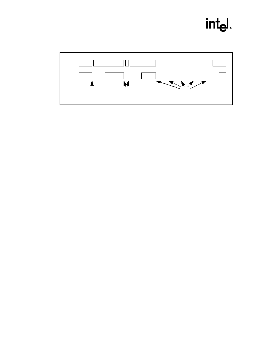
LXT972A 3.3 V Dual-Speed Fast Ethernet Transceiver
40
Datasheet
Document #: 249186
Revision #: 003
Rev. Date: August 7, 2002
3.10
Boundary Scan (JTAG1149.1) Functions
LXT972A includes a IEEE 1149.1 boundary scan test port for board level testing. All digital input,
output, and input/output pins are accessible. The BSDL file is available by contacting your local
sales office (see the back page) or by accessing the Intel web site (developer.intel.com/design/
network/).
3.10.1
Boundary Scan Interface
This interface consists of five pins (TMS, TDI, TDO, TRST, and TCK). It includes a state machine,
data register array, and instruction register. The TMS and TDI pins are internally pulled up. TCK is
internally pulled down. TDO does not have an internal pull-up or pull-down.
3.10.2
State Machine
The TAP controller is a 16 state machine driven by the TCK and TMS pins. Upon reset the
TEST_LOGIC_RESET state is entered. The state machine is also reset when TMS and TDI are
high for five TCK periods.
3.10.3
Instruction Register
After the state machine resets, the IDCODE instruction is always invoked. The decode logic
ensures the correct data flow to the Data registers according to the current instruction. Valid
instructions are listed in
Table 13
.
3.10.4
Boundary Scan Register (BSR)
Each Boundary Scan Register (BSR) cell has two stages. A flip-flop and a latch are used for the
serial shift stage and the parallel output stage. There are four modes of operation as listed in
Table
12
.
Figure 20. LED Pulse Stretching
Event
LED
Note: The direct drive LED outputs in this diagram are shown as active Low.
stretch
stretch
stretch
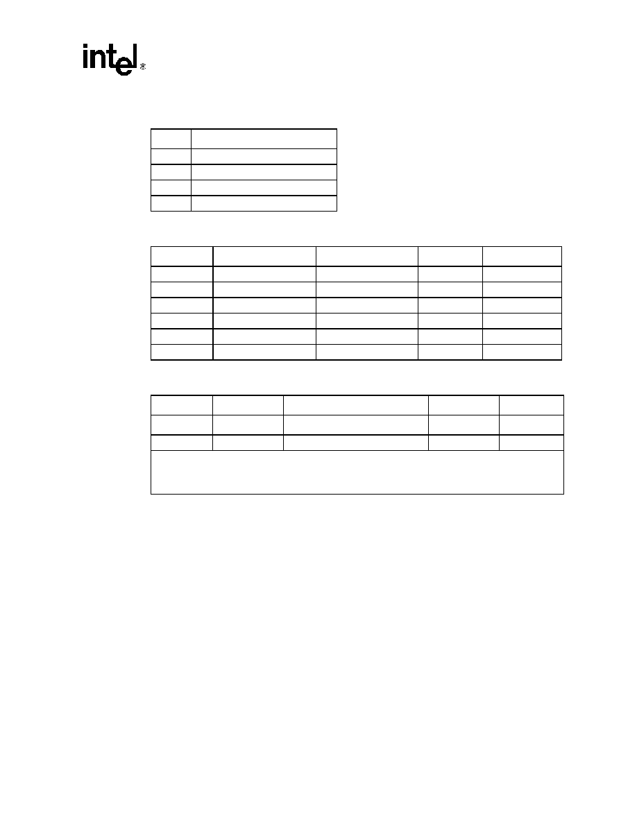
LXT972A 3.3 V Dual-Speed Fast Ethernet Transceiver
Datasheet
41
Document #: 249186
Revision #: 003
Rev. Date: August 7, 2002
Table 12. BSR Mode of Operation
Mode
Description
1
Capture
2
Shift
3
Update
4
System Function
Table 13. Supported JTAG Instructions
Name
Code
Description
Mode
Data Register
EXTEST
1111 1111 1110 1000
External Test
Test
BSR
IDCODE
1111 1111 1111 1110
ID Code Inspection
Normal
ID REG
SAMPLE
1111 1111 1111 1000
Sample Boundary
Normal
BSR
HIGHZ
1111 1111 1100 1111
Force Float
Normal
Bypass
CLAMP
1111 1111 1110 1111
Control Boundary to 1/0
Test
Bypass
BYPASS
1111 1111 1111 1111
Bypass Scan
Normal
Bypass
Table 14. Device ID Register
31:28
27:12
11:8
7:1
0
Version
Part ID (hex)
Jedec Continuation Characters
JEDEC ID
1
Reserved
XXXX
03CB
0000
111 1110
1
1. The JEDEC IS is an 8-bit identifier. The MSB is for parity and is ignored. Intel's JEDEC ID is FE (1111 1110) which
becomes 111 1110.
2. See the LXT971A/972A Specification Update (document number 249354) for the current version of the
Jedec continuation characters.
LXT972A 3.3 V Dual-Speed Fast Ethernet Transceiver
42
Datasheet
Document #: 249186
Revision #: 003
Rev. Date: August 7, 2002
4.0
Application Information
4.1
Magnetics Information
The LXT972A requires a 1:1 ratio for both the receive and transmit transformers. The transformer
isolation voltage should be rated at 2kV to protect the circuitry from static voltages across the
connectors and cables. Refer to
Table 15
for transformer requirements.
A cross-reference list of magnetic manufacturers and part numbers is available in Magnetic
Manufacturers for Networking Product Applications (document number 248991) and is found on
the Intel web site (www.Intel.com). Before committing to a specific component, designers should
contact the manufacturer for current product specifications, and validate the magnetics for the
specific application.
4.2
Typical Twisted-Pair Interface
Table 16
provides a comparison of the RJ-45 connections for NIC and switch applications in a
typical twisted-pair interface setting.
Figure 21 on page 43
shows a typical twisted-pair interface with the RJ-45 connections crossed
over for a switch configuration.
Figure 22 on page 44
provides a typical twisted-pair interface with
the RJ-45 connections configured for a NIC application.
Table 15. Magnetics Requirements
Parameter
Min
Nom
Max
Units
Test Condition
Rx turns ratio
≠
1 : 1
≠
≠
≠
Tx turns ratio
≠
1 : 1
≠
≠
≠
Insertion loss
0.0
0.6
1.1
dB
≠
Primary inductance
350
≠
≠
µH
≠
Transformer isolation
≠
1.5
≠
kV
≠
Differential to common mode rejection
40
≠
≠
dB
.1 to 60 MHz
35
≠
≠
dB
60 to 100 MHz
Return Loss
-16
≠
≠
dB
30 MHz
-10
≠
≠
dB
80 MHz
Table 16. RJ-45 Pin Comparison of NIC and Switch Twisted-Pair Interfaces
Symbol
RJ-45
Switch
NIC
TPIP
1
3
TPIN
2
6
TPOP
3
1
TPON
6
2
LXT972A 3.3 V Dual-Speed Fast Ethernet Transceiver
Datasheet
43
Document #: 249186
Revision #: 003
Rev. Date: August 7, 2002
Figure 21. Typical Twisted-Pair Interface - Switch
TPIP
TPIN
RJ-45
* = 0.001
µF / 2.0 kV
To Tw
i
s
ted-Pai
r
Net
w
ork
3
6
1
2
1:1
LXT972A
50
50
50
50
50
50
4
5
8
7
1:1
1
TPOP
TPON
VCCA
GND
0.1
µF
.01
µF
2
270 pF 5%
270 pF 5%
0.01
µF
50
1%
50
1%
*
*
3
4
0.1
µF
1. Center-tap current may be supplied from 3.3 V VCCA as shown. Additional power savings may be
realized by supplying the center-tap from a 2.5 V current source. A separate ferrite bead (rated at 50
mA) should be used to supply center-tap current.
2. The 100
transmit load termination resistor typically required is integrated in the LXT972A.
3. Magnetics without a receive pair center-tap do not require a 2 kV termination.
4. RJ-45 connections shown are for a standard switch application. For a standard NIC RJ-45 setup, see
Figure 22 on page 44
.
LXT972A 3.3 V Dual-Speed Fast Ethernet Transceiver
44
Datasheet
Document #: 249186
Revision #: 003
Rev. Date: August 7, 2002
Figure 22. Typical Twisted-Pair Interface - NIC
1. Center tap current may be supplied from 3.3 V VCCA as shown. Additional power savings may be realized by
supplying the center tap from a 2.5 V current source. A separate ferrite bead (rated at 50 mA) should be used to supply
center tap current.
2. The 100
transmit load termination resistor typically required is integrated in the LXT972A.
3. Magnetics without a receive pair center tap do not require a 2kV termination.
4. RJ-45 connections shown are for a standard NIC. Tx/Rx crossover may be required for repeater & switch applications.
Figure 23. Typical MII Interface
TPIP
TPIN
* = 0.001
µF / 2.0 kV
To T
w
i
s
t
e
d
-
P
a
i
r
Net
work
1:1
LXT972A
1:1
1
TPOP
TPON
VCCA
GND
0.1
µF
.01
µF
2
270 pF 5%
270 pF 5%
0.01
µF
50
1%
50
1%
*
*
3
6
3
8
7
5
4
1
2
50
50
50
RJ-45
50
50
50
4
0.1
µF
MAC
TX_EN
TX_ER
TXD<3:0>
TX_CLK
RX_DV
RX_ER
RXD<3:0>
CRS
COL
LXT972A
X
RJ-45
F
M
R
RX_CLK
LXT972A 3.3 V Dual-Speed Fast Ethernet Transceiver
Datasheet
45
Document #: 249186
Revision #: 003
Rev. Date: August 7, 2002
5.0
Test Specifications
Note:
Table 17
through
Table 36
and
Figure 24
through
Figure 35
represent the target specifications of
the LXT972A. These specifications are guaranteed by test except where noted "by design."
Minimum and maximum values listed in
Table 19
through
Table 36
apply over the recommended
operating conditions specified in
Table 18
.
5.1
Electrical Parameters
Table 17. Absolute Maximum Ratings
Parameter
Sym
Min
Max
Units
Supply voltage
V
CC
-0.3
4.0
V
Operating temperature
T
OPA
-15
+85
∫C
Storage temperature
T
ST
-65
+150
∫C
Caution: Exceeding these values may cause permanent damage.
Functional operation under these conditions is not implied.
Exposure to maximum rating conditions for extended periods may affect device
reliability.
Table 18. Operating Conditions
Parameter
Sym
Min
Typ
1
Max
Units
Recommended operating
temperature
LXT972A_C
(Commercial)
T
OPA
0
≠
70
∫C
Recommended supply voltage
2
Analog & Digital
Vcca, Vccd
3.14
3.3
3.45
V
I/O
Vccio
2.35
≠
3.45
V
V
CC
current
100BASE-TX
I
CC
≠
92
110
mA
10BASE-T
I
CC
≠
66
82
mA
Hard Power Down
I
CC
≠
≠
1
mA
Soft Power Down
Icc
≠
51
≠
Auto-Negotiation
I
CC
≠
90
110
mA
1. Typical values are at 25 ∞C and are for design aid only; not guaranteed and not subject to production testing.
2. Voltages with respect to ground unless otherwise specified.
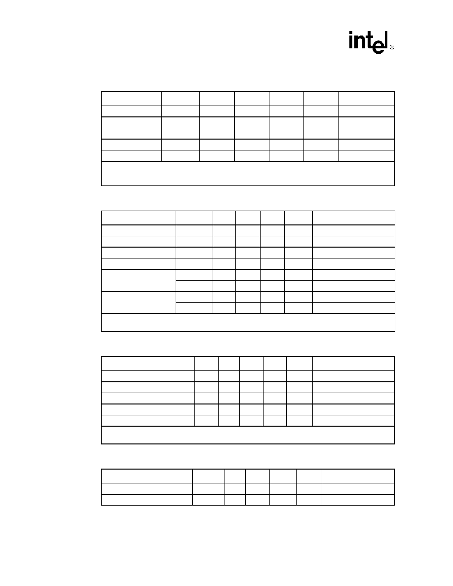
LXT972A 3.3 V Dual-Speed Fast Ethernet Transceiver
46
Datasheet
Document #: 249186
Revision #: 003
Rev. Date: August 7, 2002
Table 19. Digital I/O Characteristics
1
Parameter
Symbol
Min
Typ
2
Max
Units
Test Conditions
Input Low voltage
V
IL
≠
≠
0.8
V
≠
Input High voltage
V
IH
2.0
≠
≠
V
≠
Input current
I
I
-10
≠
10
µA
0.0 < V
I
< V
CC
Output Low voltage
V
OL
≠
≠
0.4
V
I
OL
= 4 mA
Output High voltage
V
OH
2.4
≠
≠
V
I
OH
= -4 mA
1. Applies to all pins except MII, LED and XI/XO pins. Refer to
Table 20
for MII I/O Characteristics,
Table 21
for XI/
XO and
Table 22
for LED Characteristics.
2. Typical values are at 25 ∞C and are for design aid only; not guaranteed and not subject to production testing.
Table 20. Digital I/O Characteristics - MII Pins
Parameter
Symbol
Min
Typ
1
Max
Units
Test Conditions
Input Low voltage
V
IL
≠
≠
0.8
V
≠
Input High voltage
V
IH
2.0
≠
≠
V
≠
Input current
I
I
-10
≠
10
µA
0.0 < V
I
< VCCIO
Output Low voltage
V
OL
≠
≠
0.4
V
I
OL
= 4 mA
Output High voltage
V
OH
2.2
≠
≠
V
I
OH
= -4 mA, VCCIO = 3.3 V
V
OH
2.0
≠
≠
V
I
OH
= -4 mA, VCCIO = 2.5 V
Driver output resistance
(Line driver output enabled)
R
O2
≠
100
≠
VCCIO = 2.5 V
R
O2
≠
100
≠
VCCIO = 3.3 V
1. Typical values are at 25 ∞C and are for design aid only; not guaranteed and not subject to production testing.
2. Parameter is guaranteed by design; not subject to production testing.
Table 21. I/O Characteristics - REFCLK/XI and XO Pins
Parameter
Sym
Min
Typ
1
Max
Units
Test Conditions
Input Low Voltage
V
IL
≠
≠
0.8
V
≠
Input High Voltage
V
IH
2.0
≠
≠
V
≠
Input Clock Frequency Tolerance
2
f
≠
≠
±
100
ppm
≠
Input Clock Duty Cycle
2
Tdc
35
≠
65
%
≠
Input Capacitance
C
IN
≠
3.0
≠
pF
≠
1. Typical values are at 25 ∞C and are for design aid only; not guaranteed and not subject to production testing.
2. Parameter is guaranteed by design; not subject to production testing.
Table 22. I/O Characteristics - LED/CFG Pins
Parameter
Symbol
Min
Typ
Max
Units
Test Conditions
Input Low Voltage
V
IL
≠
≠
0.8
V
≠
Input High Voltage
V
IH
2.0
≠
≠
V
≠
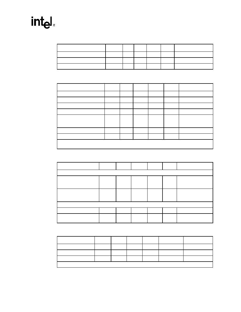
LXT972A 3.3 V Dual-Speed Fast Ethernet Transceiver
Datasheet
47
Document #: 249186
Revision #: 003
Rev. Date: August 7, 2002
Input Current
I
I
-10
≠
10
µA
0 < V
I
< VCCIO
Output Low Voltage
V
OL
≠
≠
0.4
V
I
OL
= 10 mA
Output High Voltage
V
OH
2.0
≠
≠
V
I
OH
= -10 mA
Table 23. 100BASE-TX Transceiver Characteristics
Parameter
Sym
Min
Typ
1
Max
Units
Test Conditions
Peak differential output voltage
V
P
0.95
≠
1.05
V
Note 2
Signal amplitude symmetry
Vss
98
≠
102
%
Note 2
Signal rise/fall time
T
RF
3.0
≠
5.0
ns
Note 2
Rise/fall time symmetry
T
RFS
≠
≠
0.5
ns
Note 2
Duty cycle distortion
D
CD
35
50
65
%
Offset from 16ns pulse
width at 50% of pulse
peak
Overshoot/Undershoot
V
OS
≠
≠
5
%
≠
Jitter (measured differentially)
≠
≠
≠
1.4
ns
≠
1. Typical values are at 25 ∞C and are for design aid only; not guaranteed and not subject to production testing.
2. Measured at the line side of the transformer, line replaced by 100
(+/-1%) resistor.
Table 24. 10BASE-T Transceiver Characteristics
Parameter
Sym
Min
Typ
Max
Units
Test Conditions
Transmitter
Peak differential output
voltage
V
OP
2.2
2.5
2.8
V
With transformer, line
replaced by 100
resistor
Transition timing jitter added
by the MAU and PLS sections
-
0
2
11
ns
After line model specified
by IEEE 802.3 for
10BASE-T MAU
Receiver
Receive Input Impedance
Z
IN
-
-
22
k
Differential Squelch
Threshold
V
DS
300
420
585
mV
Table 25. 10BASE-T Link Integrity Timing Characteristics
Parameter
Sym
Min
Typ
Max
Units
Test Conditions
Time Link Loss Receive
T
LL
50
≠
150
ms
≠
Link Pulse
T
LP
2
≠
7
Link Pulses
≠
Link Min Receive Timer
T
LR
M
IN
2
≠
7
ms
≠
1. Typical values are at 25 ∞C and are for design aid only; not guaranteed and not subject to production testing.
Table 22. I/O Characteristics - LED/CFG Pins (Continued)
Parameter
Symbol
Min
Typ
Max
Units
Test Conditions
LXT972A 3.3 V Dual-Speed Fast Ethernet Transceiver
48
Datasheet
Document #: 249186
Revision #: 003
Rev. Date: August 7, 2002
Link Max Receive Timer
T
LR
M
AX
50
≠
150
ms
≠
Link Transmit Period
Tlt
8
≠
24
ms
≠
Link Pulse Width
Tlpw
60
≠
150
ns
≠
Table 26. LXT972A Thermal Characteristics
Parameter
LXT972ALC
Package
10 x 10 x 1.4 64LQFP
Theta-JA
58 C/W
Theta-JC
27 C/W
Psi - JT
3.4 C/W
Table 25. 10BASE-T Link Integrity Timing Characteristics
Parameter
Sym
Min
Typ
Max
Units
Test Conditions
1. Typical values are at 25 ∞C and are for design aid only; not guaranteed and not subject to production testing.
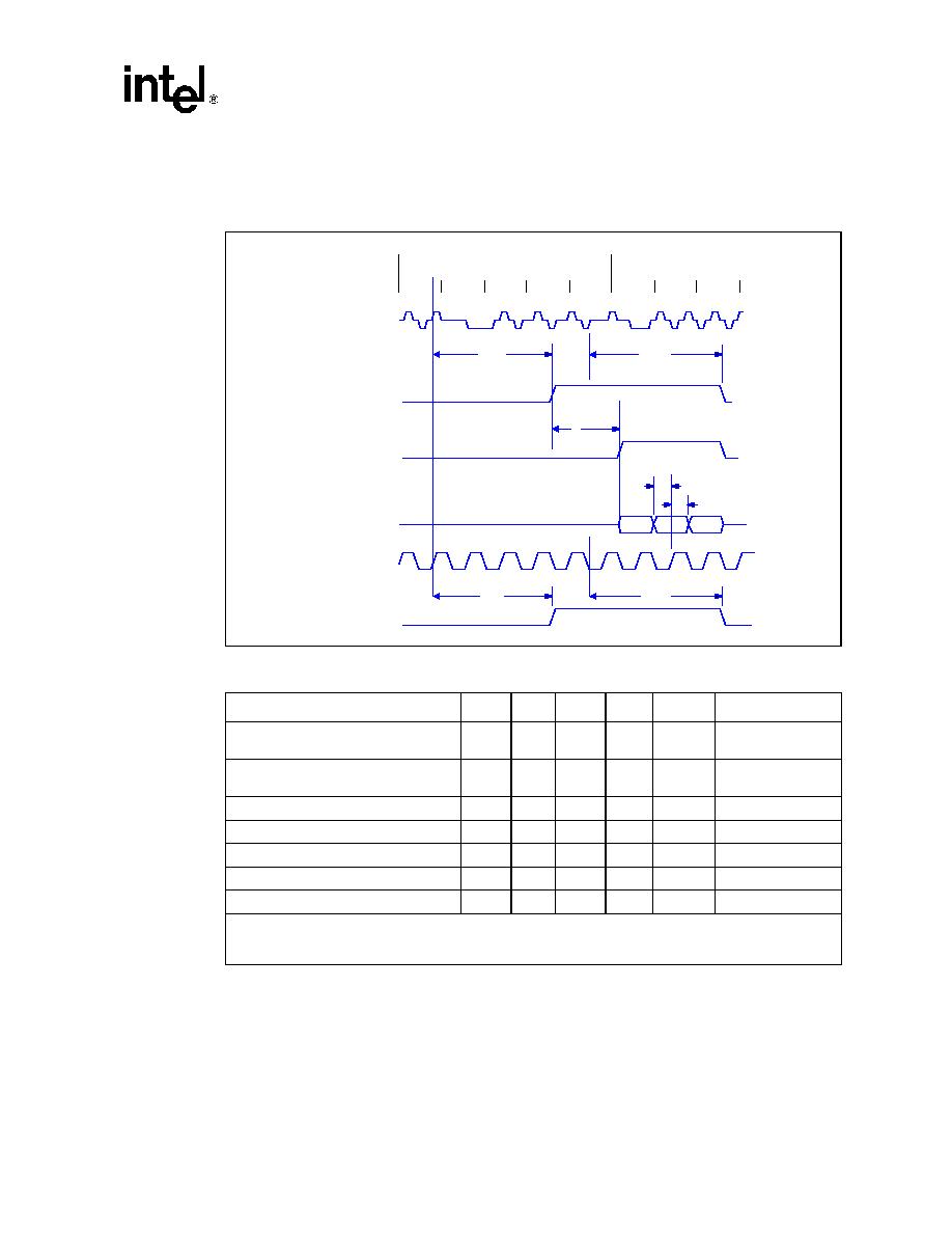
LXT972A 3.3 V Dual-Speed Fast Ethernet Transceiver
Datasheet
49
Document #: 249186
Revision #: 003
Rev. Date: August 7, 2002
5.2
Timing Diagrams
Figure 24. 100BASE-TX Receive Timing - 4B Mode
Table 27. 100BASE-TX Receive Timing Parameters - 4B Mode
Parameter
Sym
Min
Typ
1
Max
Units
2
Test Conditions
RXD<3:0>, RX_DV, RX_ER setup
to RX_CLK High
t1
10
≠
≠
ns
≠
RXD<3:0>, RX_DV, RX_ER hold
from RX_CLK High
t2
10
≠
≠
ns
≠
CRS asserted to RXD<3:0>, RX_DV
t3
3
≠
5
BT
≠
Receive start of "J" to CRS asserted
t4
12
≠
16
BT
≠
Receive start of "T" to CRS de-asserted
t5
10
≠
17
BT
≠
Receive start of "J" to COL asserted
t6
16
≠
22
BT
≠
Receive start of "T" to COL de-asserted
t7
17
≠
20
BT
≠
1. Typical values are at 25 ∞C and are for design aid only; not guaranteed and not subject to production testing.
2. BT is the duration of one bit as transferred to and from the MAC and is the reciprocal of the bit rate. 100BASE-T bit
time = 10
-8
s or 10 ns.
t4
t5
t3
t6
t7
0 ns
250 ns
CRS
RX_DV
RXD<3:0>
RX_CLK
COL
t1
t2
TPI
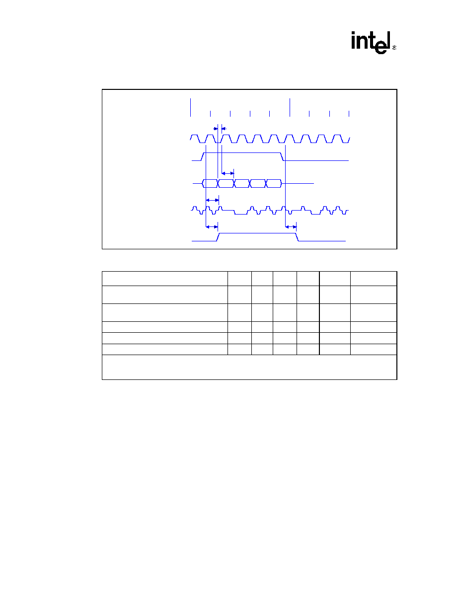
LXT972A 3.3 V Dual-Speed Fast Ethernet Transceiver
50
Datasheet
Document #: 249186
Revision #: 003
Rev. Date: August 7, 2002
Figure 25. 100BASE-TX Transmit Timing - 4B Mode
Table 28. 100BASE-TX Transmit Timing Parameters
-
4B Mode
Parameter
Sym
Min
Typ
1
Max
Units
2
Test Conditions
TXD<3:0>, TX_EN, TX_ER setup to TX_CLK
High
t1
12
≠
≠
ns
≠
TXD<3:0>, TX_EN, TX_ER hold from TX_CLK
High
t2
0
≠
≠
ns
≠
TX_EN sampled to CRS asserted
t3
20
≠
24
BT
≠
TX_EN sampled to CRS de-asserted
t4
24
≠
28
BT
≠
TX_EN sampled to TPO out (Tx latency)
t5
5.3
≠
5.7
BT
≠
1. Typical values are at 25 ∞C and are for design aid only; not guaranteed and not subject to production testing.
2. BT is the duration of one bit as transferred to and from the MAC and is the reciprocal of the bit rate. 100BASE-T bit
time = 10
-8
s or 10 ns.
t1
t2
t5
t3
t4
0ns
250ns
TXCLK
TX_EN
TXD<3:0>
TPO
CRS
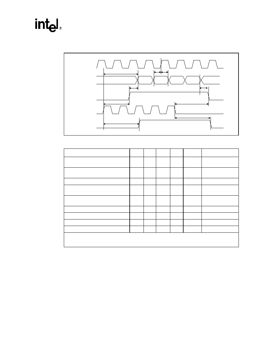
LXT972A 3.3 V Dual-Speed Fast Ethernet Transceiver
Datasheet
51
Document #: 249186
Revision #: 003
Rev. Date: August 7, 2002
Figure 26. 10BASE-T Receive Timing
Table 29. 10BASE-T Receive Timing Parameters
Parameter
Sym
Min
Typ
1
Max
Units
2
Test Conditions
RXD, RX_DV, RX_ER Setup to RX_CLK
High
t1
10
≠
≠
ns
≠
RXD, RX_DV, RX_ER Hold from
RX_CLK High
t2
10
≠
≠
ns
≠
TPIP/N in to RXD out (Rx latency)
t3
4.2
≠
6.6
BT
≠
CRS asserted to RXD, RX_DV, RX_ER
asserted
t4
5
≠
32
BT ≠
RXD, RX_DV, RX_ER de-asserted to CRS
de-asserted
t5
0.3
≠
0.5
BT
≠
TPI in to CRS asserted
t6
2
≠
28
BT
≠
TPI quiet to CRS de-asserted
t7
6
≠
10
BT
≠
TPI in to COL asserted
t8
1
≠
31
BT
≠
TPI quiet to COL de-asserted
t9
5
≠
10
BT
≠
1. Typical values are at 25 ∞C and are for design aid only; not guaranteed and not subject to production testing.
2. BT is the duration of one bit as transferred to and from the MAC and is the reciprocal of the bit rate. 10BASE-T bit
time = 10
-7
s or 100 ns.
RX_CLK
RXD,
RX_DV,
RX_ER
CRS
TPI
t
3
t
4
t
2
t
6
t
1
t
7
t
5
COL
t
8
t
9

LXT972A 3.3 V Dual-Speed Fast Ethernet Transceiver
52
Datasheet
Document #: 249186
Revision #: 003
Rev. Date: August 7, 2002
Figure 27. 10BASE-T Transmit Timing
Table 30. 10BASE-T Transmit Timing Parameters
Parameter
Sym
Min
Typ
1
Max
Units
2
Test Conditions
TXD, TX_EN, TX_ER setup to TX_CLK
High
t1
10
≠
≠
ns
≠
TXD, TX_EN, TX_ER hold from TX_CLK
High
t2
0
≠
≠
ns
≠
TX_EN sampled to CRS asserted
t3
≠
2
≠
BT
≠
TX_EN sampled to CRS de-asserted
t4
≠
1
≠
BT
≠
TX_EN sampled to TPO out (Tx latency)
t5
≠
72.5
≠
BT
≠
1. Typical values are at 25 ∞C and are for design aid only; not guaranteed and not subject to production testing.
2. BT is the duration of one bit as transferred to and from the MAC and is the reciprocal of the bit rate. 10BASE-T bit
time = 10
-7
s or 100 ns.
TX_CLK
TXD,
TX_EN,
TX_ER
CRS
TPO
t
1
t
3
t
4
t
5
t
2
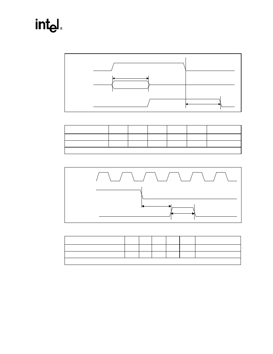
LXT972A 3.3 V Dual-Speed Fast Ethernet Transceiver
Datasheet
53
Document #: 249186
Revision #: 003
Rev. Date: August 7, 2002
Figure 28. 10BASE-T Jabber and Unjabber Timing
Table 31. 10BASE-T Jabber and Unjabber Timing Parameters
Parameter
Sym
Min
Typ
1
Max
Units
Test Conditions
Maximum transmit time
t1
20
≠
150
ms
≠
Unjab time
t2
250
≠
750
ms
≠
1. Typical values are at 25 ∞C and are for design aid only; not guaranteed and not subject to production testing.
Figure 29. 10BASE-T SQE (Heartbeat) Timing
Table 32. 10BASE-T SQE Timing Parameters
Parameter
Sym
Min
Typ
1
Max
Units
Test Conditions
COL (SQE) Delay after TX_EN off
t1
0.65
≠
1.6
us
≠
COL (SQE) Pulse duration
t2
0.5
≠
1.5
us
≠
1. Typical values are at 25 ∞C and are for design aid only; not guaranteed and not subject to production testing.
TXD
COL
t
1
t
2
TX_EN
TX_CLK
TX_EN
t
1
t
2
COL
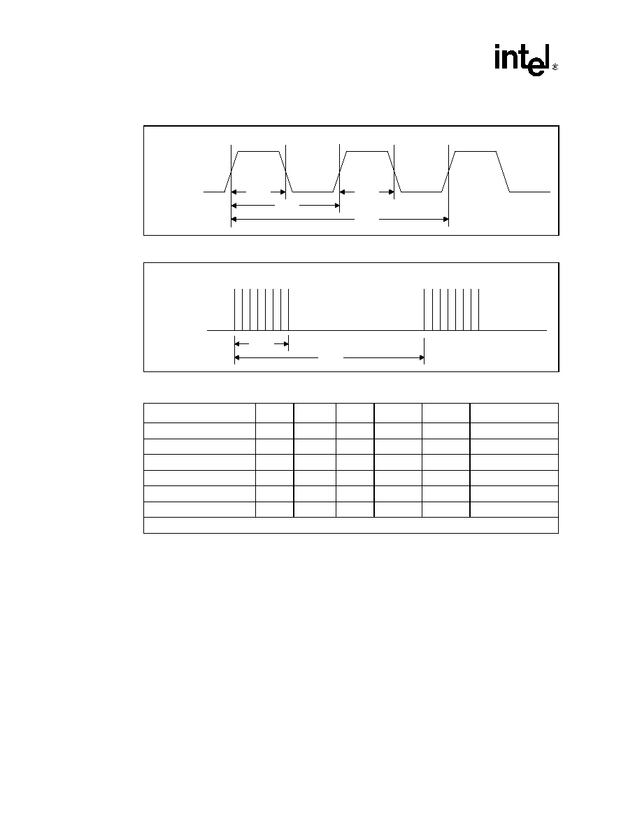
LXT972A 3.3 V Dual-Speed Fast Ethernet Transceiver
54
Datasheet
Document #: 249186
Revision #: 003
Rev. Date: August 7, 2002
Figure 30. Auto Negotiation and Fast Link Pulse Timing
Figure 31. Fast Link Pulse Timing
Table 33. Auto Negotiation and Fast Link Pulse Timing Parameters
Parameter
Sym
Min
Typ
1
Max
Units
Test Conditions
Clock/Data pulse width
t1
≠
100
≠
ns
≠
Clock pulse to Data pulse
t2
55.5
≠
63.8
µs
≠
Clock pulse to Clock pulse
t3
123
≠
127
µs
≠
FLP burst width
t4
≠
2
≠
ms
≠
FLP burst to FLP burst
t5
8
12
24
ms
≠
Clock/Data pulses per burst
≠
17
≠
33
ea
≠
1. Typical values are at 25 ∞C and are for design aid only; not guaranteed and not subject to production testing.
TPO
t1
t1
t2
t3
Clock Pulse
Data Pulse
Clock Pulse
TPO
t4
t5
FLP Burst
FLP Burst
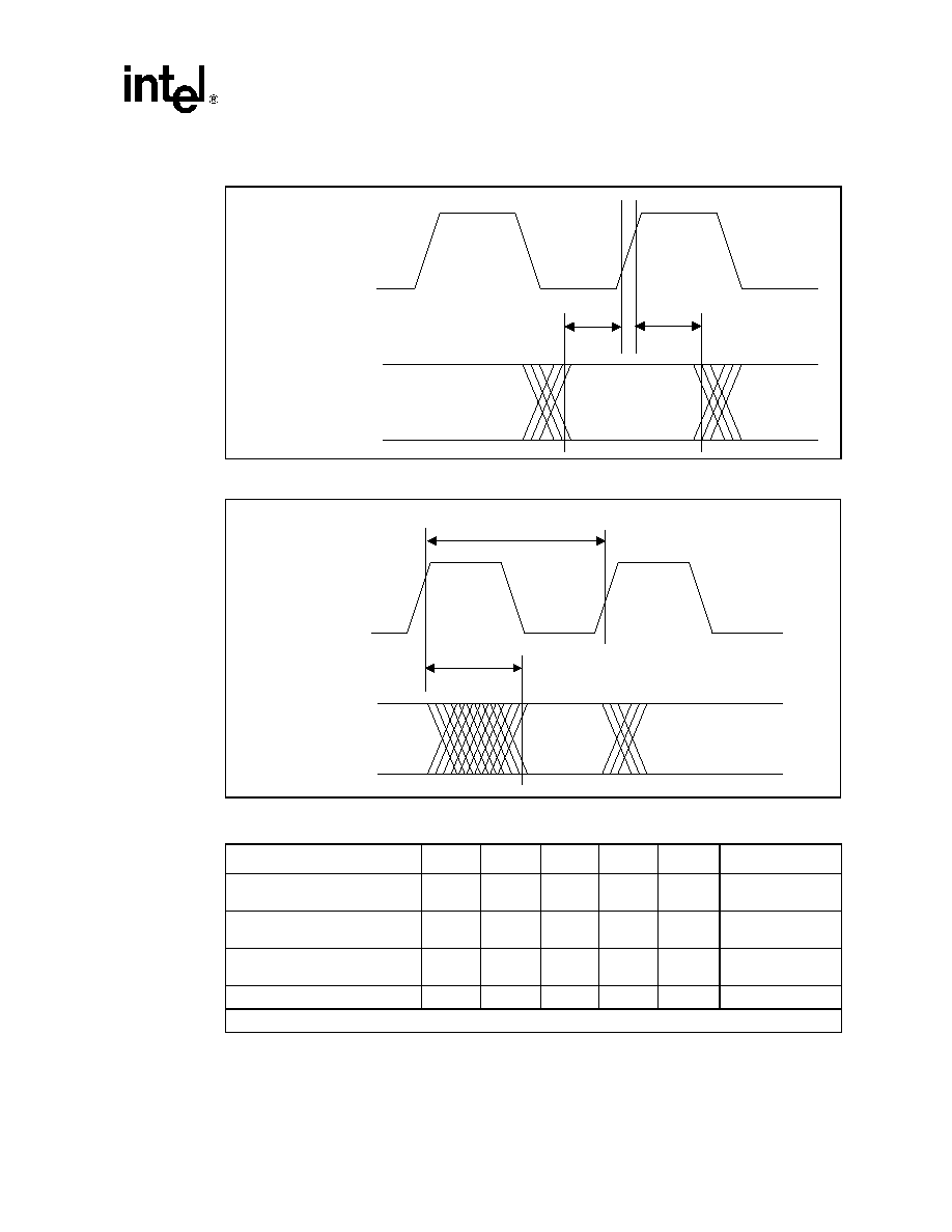
LXT972A 3.3 V Dual-Speed Fast Ethernet Transceiver
Datasheet
55
Document #: 249186
Revision #: 003
Rev. Date: August 7, 2002
Figure 32. MDIO Input Timing
Figure 33. MDIO Output Timing
Table 34. MDIO Timing Parameters
Parameter
Sym
Min
Typ
1
Max
Units
Test Conditions
MDIO setup before MDC, sourced
by STA
t1
10
≠
≠
ns
≠
MDIO hold after MDC, sourced by
STA
t2
5
≠
≠
ns
≠
MDC to MDIO output delay, source
by PHY
t3
≠
≠
150
ns
≠
MDC period
t4
125
≠
≠
ns
MDC = 8 MHz
1. Typical values are at 25∞ C and are for design aid only; not guaranteed and not subject to production testing.
t1
MDC
MDIO
t2
t3
MDC
MDIO
t4
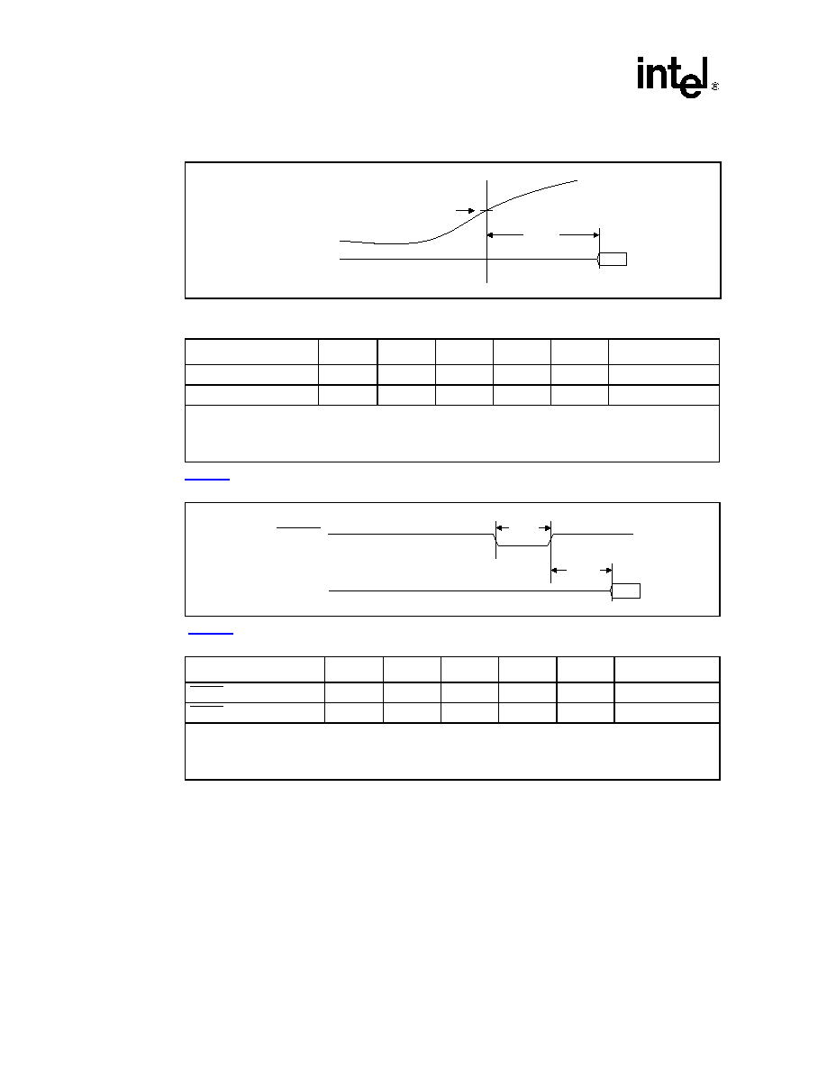
LXT972A 3.3 V Dual-Speed Fast Ethernet Transceiver
56
Datasheet
Document #: 249186
Revision #: 003
Rev. Date: August 7, 2002
Figure 34. Power-Up Timing
Table 35. Power-Up Timing Parameters
Parameter
Sym
Min
Typ
1
Max
Units
Test Conditions
Voltage threshold
v1
≠
2.9
≠
V
≠
Power Up delay
2
t1
≠
≠
300
µs
≠
1. Typical values are at 25∞ C and are for design aid only; not guaranteed and not subject to production testing.
2. Power Up Delay is specified as a maximum value because it refers to the PHY's guaranteed performance - the PHY
comes out of reset after a delay of No MORE Than 300
µ
s. System designers should consider this as a minimum
value - After threshold v1 is reached, the MAC should delay No LESS Than 300
µ
s
before accessing the MDIO port.
Figure 35. RESET Pulse Width and Recovery Timing
Table 36. RESET Pulse Width and Recovery Timing Parameters
Parameter
Sym
Min
Typ
1
Max
Units
Test Conditions
RESET pulse width
t1
10
≠
≠
ns
≠
RESET recovery delay
2
t2
≠
≠
300
µs
≠
1. Typical values are at 25∞ C and are for design aid only; not guaranteed and not subject to production testing.
2. Reset Recovery Delay is specified as a maximum value because it refers to the PHY's guaranteed performance - the
PHY comes out of reset after a delay of No MORE Than 300
µ
s. System designers should consider this as a minimum
value - After de-asserting RESET*, the MAC should delay No LESS Than 300
µ
s before accessing the MDIO port.
t1
VCC
MDIO,etc
v1
t2
RESET
MDIO,etc
t1

LXT972A 3.3 V Dual-Speed Fast Ethernet Transceiver
Datasheet
57
Document #: 249186
Revision #: 003
Rev. Date: August 7, 2002
6.0
Register Definitions
The LXT972A register set includes multiple 16-bit registers. Refer to
Table 37
for a complete
register listing.
∑
Base registers (0 through 8) are defined in accordance with the "Reconciliation Sublayer and
Media Independent Interface" and "Physical Layer Link Signaling for 10/100 Mbps Auto-
Negotiation" sections of the IEEE 802.3 standard.
∑
Additional registers are defined in accordance with the IEEE 802.3 standard for adding unique
chip functions.
Table 37. Register Set
Address
Register Name
Bit Assignments
0
Control Register
Refer to
Table 39 on page 60
1
Status Register #1
Refer to
Table 40 on page 61
2
PHY Identification Register 1
Refer to
Table 41 on page 62
3
PHY Identification Register 2
Refer to
Table 42 on page 62
4
Auto-Negotiation Advertisement Register
Refer to
Table 43 on page 63
5
Auto-Negotiation Link Partner Base Page Ability Register
Refer to
Table 44 on page 64
6
Auto-Negotiation Expansion Register
Refer to
Table 45 on page 65
7
Auto-Negotiation Next Page Transmit Register
Refer to
Table 46 on page 65
8
Auto-Negotiation Link Partner Received Next Page
Register
Refer to
Table 47 on page 66
9
1000BASE-T/100BASE-T2 Control Register
Not Implemented
10
1000BASE-T/100BASE-T2 Status Register
Not Implemented
15
Extended Status Register
Not Implemented
16
Port Configuration Register
Refer to
Table 48 on page 66
17
Status Register #2
Refer to
Table 49 on page 67
18
Interrupt Enable Register
Refer to
Table 50 on page 68
19
Interrupt Status Register
Refer to
Table 51 on page 68
20
LED Configuration Register
Refer to
Table 52 on page 70
21-25
Reserved
≠
26
27-30
Transmit Control Register
Refer to
Table 54 on page 72
LXT972A 3.3 V Dual-Speed Fast Ethernet Transceiver
58
Datasheet
Document #: 249186
Revision #: 003
Rev. Date: August 7, 2002
T
a
ble 38.
Register
Bit M
a
p
Reg T
i
tle
Bit Fields
Addr
B1
5
B
1
4
B13
B
1
2
B1
1
B
1
0
B
9
B8
B7
B6
B5
B
4
B3
B2
B1
B0
Con
t
r
o
l Register
Contr
o
l
R
e
s
e
t
L
o
opb
ack
Speed Select
A/N En
able
Power Down
Isolate
R
e
-start A/
N
Duplex Mo
de
CO
L
T
e
st
Spee
d
Select
Re
s
e
r
v
e
d
0
S
t
at
u
s
Register
St
a
t
u
s
10
0B
as
e-
T4
100B
ase-X
Full
Duplex
100Base-X
Half
Duplex
10
M
b
ps
Full
Duplex
10
M
b
p
s
Half
Duplex
100Base- T2 Full Duplex
10
0B
ase
-
T
2
Half
Duplex
Ex
tend
ed
St
a
t
u
s
Res
e
r
v
ed
MF
Pr
eamble
Suppr
e
s
s
A/N
C
o
mplete
Rem
o
t
e
Fa
ul
t
A/N
Ability
Li
n
k
S
t
a
t
us
Ja
b
b
e
r
Detect
Ex
tend
ed
C
a
pability
1
PHY ID Registers
PH
Y ID 1
1
5
1
4
1
3
1
2
1
1
1
0
98
76
543
21
0
2
PH
Y
ID
2
PHY ID No
MFR
Model No
MFR R
e
v No
3
Auto-Negotiation Advert
is
ement Regis
t
e
r
A/N Advert
is
e
Next Page
R
e
s
e
r
v
ed
Remo
te
Faul
t
Res
e
rv
ed
Asymm
Pause
Pause
10
0B
ase
-
T4
10
0B
ase-
TX Full Duplex
10
0B
as
e-
TX
10
Bas
e
-T
Full
Duplex
10B
a
se-T
IE
EE Selector
Field
4
Auto-Negotiation Link
P
a
rtner
Base Page Abil
it
y Register
A/N Lin
k
Abilit
y
Next Page
Ack
Remo
te
Faul
t
Res
e
rv
ed
Asymm
Pause
Pause
10
0B
ase
-
T4
10
0B
ase-
TX Full Duplex
10
0B
as
e-
TX
10
Bas
e
-T
Full
Duplex
10B
a
se-T
IE
EE Selector
Field
5
Auto-Negotiation
Expansion Regis
t
e
r
A/N Exp
a
nsi
o
n
Res
e
rv
ed
Base Page
Parallel Detect Fa
ul
t
Link
Par
t
ner
Ne
xt Page Able
Next Page
Able
Page
R
eceived
Link
Partn
e
r
A/N Able
6
Auto-Negotiation
Next Pa
ge T
r
ansmit Register
A/N Next P
a
ge
Tx
m
i
t
Next Page
R
e
s
e
r
v
ed
Messag
e
Pa
g
e
Ack
2
T
oggle
M
es
sage
/ Unf
o
r
m
atted Code F
i
eld
7
Auto-Negotiation Link
P
a
rtn
er Next Page Receive Register
A/N Link Next
Pag
e
Next Page
Ack
Messag
e
Pa
g
e
Ack
2
T
oggle
M
es
sage
/ Unf
o
r
m
atted Code F
i
eld
8
Configuration Register
Port Config
Reser
v
ed
For
ce Link Pass
Txmit Dis
a
ble
B
y
p
a
ss
Scrambler
(1
00T
X)
Reser
v
ed
)
Jab
b
er
(1
0T
)
SQE
(1
0T)
TP
Lo
op
back
(1
0T
)
CRS Select
(1
0T
)
Reserv
ed
PR
E_
EN
R
e
served
R
e
se
rved
Alternate Next Page
Reser
v
ed
1
6
LXT972A 3.3 V Dual-Speed Fast Ethernet Transceiver
Datasheet
59
Document #: 249186
Revision #: 003
Rev. Date: August 7, 2002
S
t
a
t
us
Re
gis
t
er #2
S
t
atus Register
#2
Re
s
e
rv
e
d
10
/10
0
Mo
de
T
r
ansmit St
a
t
u
s
Receive St
a
t
u
s
Collision
St
a
t
u
s
Lin
k
Duplex Mo
de
Auto-Neg
A
u
to-
Neg
C
o
mplete
Reserved
P
o
larity
Paus
e
E
rror
R
eserved
R
eserved
1
7
Interrupt Enable Register
Interrupt E
n
able
Reser
v
ed
Res
e
rv
ed
A
u
to-
Neg
Mask
Speed Mask
Duplex Mask
Link M
a
s
k
Res
e
r
v
ed
R
e
served
In
terru
pt
En
a
b
l
e
Te
s
t
In
t
e
rr
u
p
t
18
Interrupt S
t
atus Register
Interrupt
St
a
t
u
s
Reser
v
ed
Res
e
rv
ed
A
u
to-
Neg
Done
Speed Chan
ge
Duplex Ch
ang
e
Link
Ch
a
n
g
e
Res
e
rv
ed
MD
In
t
e
r
r
u
p
t
R
e
served
Reserv
ed
1
9
LED Configuration
Register
L
E
D Config
LED1
L
ED2
L
ED3
L
ED Freq
Pulse St
r
e
t
c
h
Re
s
e
rv
e
d
2
0
Digital Config Regis
t
e
r
Digital Config
Reserved
S
t
r
o
ng
Dig
i
ta
l
Pac
s
Re
se
rv
ed
Sh
ow
Sym
bol
Error
Res
e
rv
ed
26
T
r
ansmit Contr
o
l
Register
Tr
a
n
s
.
C
o
n
t
r
o
l
Reser
v
e
d
T
r
ansmit
Lo
w Pwr
Po
rt Rise T
i
me C
o
n
t
rol
R
eser
ved
3
0
T
a
ble 38.
Register
Bit Map (Continued)
Reg T
i
tle
Bit Fields
Add
r
B
1
5
B
1
4
B1
3
B
12
B1
1
B
10
B9
B
8
B7
B6
B5
B4
B
3
B2
B1
B
0
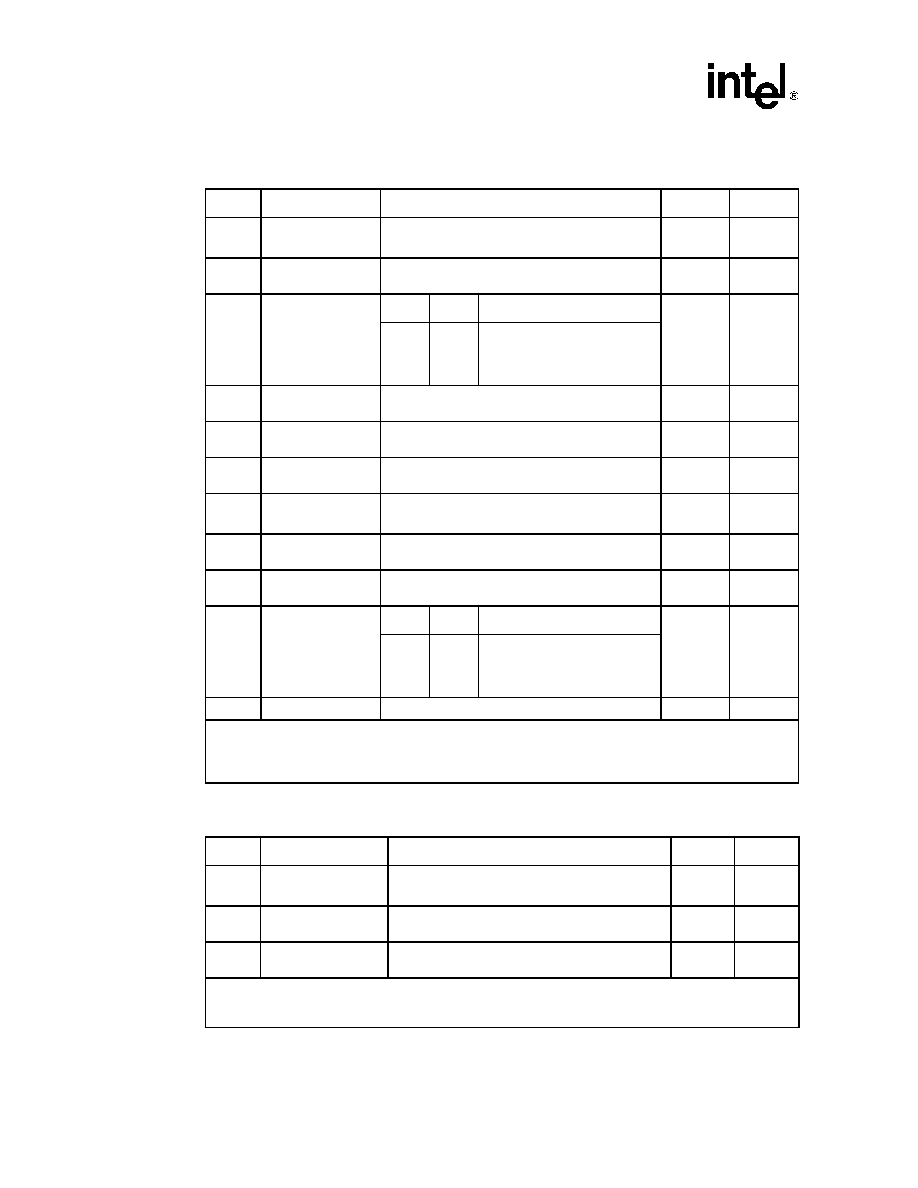
LXT972A 3.3 V Dual-Speed Fast Ethernet Transceiver
60
Datasheet
Document #: 249186
Revision #: 003
Rev. Date: August 7, 2002
Table 39. Control Register (Address 0)
Bit
Name
Description
Type
1
Default
0.15
Reset
1 = PHY reset
0 = Normal operation
R/W
SC
0
0.14
Loopback
1 = Enable loopback mode
0 = Disable loopback mode
R/W
0
0.13
Speed Selection
0.6
0.13
Speed Selected
R/W
Note 2
1
1
0
0
1
0
1
0
Reserved
1000 Mbps (not supported)
100 Mbps
10 Mbps
0.12
Auto-Negotiation
Enable
1 = Enable Auto-Negotiation Process
0 = Disable Auto-Negotiation Process
R/W
Note 2
0.11
Power-Down
1 = Power-down
0 = Normal operation
R/W
0
0.10
Isolate
1 = Electrically isolate PHY from MII
0 = Normal operation
R/W
0
0.9
Restart
Auto-Negotiation
1 = Restart Auto-Negotiation Process
0 = Normal operation
R/W
SC
0
0.8
Duplex Mode
1 = Full Duplex
0 = Half Duplex
R/W
Note 2
0.7
Collision Test
1 = Enable COL signal test
0 = Disable COL signal test
R/W
0
0.6
Speed Selection
0.6
0.13
Speed Selected
R/W
0
1
1
0
0
1
0
1
0
Reserved
1000 Mbps (not supported)
100 Mbps
10 Mbps
0.5:0
Reserved
Write as 0, ignore on Read
R/W
00000
1. R/W = Read/Write
RO = Read Only
SC = Self Clearing
2. Default value of bits 0.12, 0.13 and 0.8 are determined by the LED/CFG pins (refer to
Table 9 on page 25
).
Table 40. MII Status Register #1 (Address 1)
Bit
Name
Description
Type
1
Default
1.15
100BASE-T4
Not Supported
1 = PHY able to perform 100BASE-T4
0 = PHY not able to perform 100BASE-T4
RO
0
1.14
100BASE-X Full-
Duplex
1 = PHY able to perform full-duplex 100BASE-X
0 = PHY not able to perform full-duplex 100BASE-X
RO
1
1.13
100BASE-X Half-
Duplex
1 = PHY able to perform half-duplex 100BASE-X
0 = PHY not able to perform half-duplex 100BASE-X
RO
1
1. RO = Read Only
LL = Latching Low
LH = Latching High
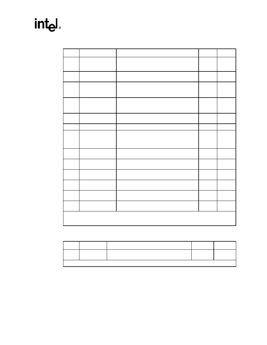
LXT972A 3.3 V Dual-Speed Fast Ethernet Transceiver
Datasheet
61
Document #: 249186
Revision #: 003
Rev. Date: August 7, 2002
1.12
10 Mbps Full-Duplex
1 = PHY able to operate at 10 Mbps in full-duplex mode
0 = PHY not able to operate at 10 Mbps full-duplex
mode
RO
1
1.11
10 Mbps Half-Duplex
1 = PHY able to operate at 10 Mbps in half-duplex mode
0 = PHY not able to operate at 10 Mbps in half-duplex
RO
1
1.10
100BASE-T2 Full-
Duplex
Not Supported
1 = PHY able to perform full-duplex 100BASE-T2
0 = PHY not able to perform full-duplex 100BASE-T2
RO
0
1.9
100BASE-T2 Half-
Duplex
Not Supported
1 = PHY able to perform half duplex 100BASE-T2
0 = PHY not able to perform half-duplex 100BASE-T2
RO
0
1.8
Extended Status
1 = Extended status information in register 15
0 = No extended status information in register 15
RO
0
1.7
Reserved
1 = ignore when read
RO
0
1.6
MF Preamble
Suppression
1 = PHY accepts management frames with preamble
suppressed
0 = PHY will not accept management frames with
preamble suppressed
RO
0
1.5
Auto-Negotiation
Complete
1 = Auto-negotiation complete
0 = Auto-negotiation not complete
RO
0
1.4
Remote Fault
1 = Remote fault condition detected
0 = No remote fault condition detected
RO/LH
0
1.3
Auto-Negotiation
Ability
1 = PHY is able to perform Auto-Negotiation
0 = PHY is not able to perform Auto-Negotiation
RO
1
1.2
Link Status
1 = Link is up
0 = Link is down
RO/LL
0
1.1
Jabber Detect
1 = Jabber condition detected
0 = Jabber condition not detected
RO/LH
0
1.0
Extended Capability
1 = Extended register capabilities
0 = Basic register capabilities
RO
1
Table 41. PHY Identification Register 1 (Address 2)
Bit
Name
Description
Type
1
Default
2.15:0
PHY ID Number
The PHY identifier composed of bits 3 through 18 of the
OUI.
RO
0013 hex
1. RO = Read Only
Table 40. MII Status Register #1 (Address 1)
Bit
Name
Description
Type
1
Default
1. RO = Read Only
LL = Latching Low
LH = Latching High

LXT972A 3.3 V Dual-Speed Fast Ethernet Transceiver
62
Datasheet
Document #: 249186
Revision #: 003
Rev. Date: August 7, 2002
Table 42. PHY Identification Register 2 (Address 3)
Bit
Name
Description
Type
1
Default
3.15:10
PHY ID number
The PHY identifier composed of bits 19
through 24 of the OUI.
RO
011110
3.9:4
Manufacturer's
model number
6 bits containing manufacturer's part
number.
RO
001110
3.3:0
Manufacturer's
revision number
4 bits containing manufacturer's revision
number.
RO
xxxx
(See LXT971A/972A
Specification Update)
1. RO = Read Only
Figure 36. PHY Identifier Bit Mapping
0
0 0 0 0 0
0
0
0 0
0 0 0 1 0 0 1 1 0 1 1 1 1 0 0 0 1 1 1 0 0 0
a
b c
r s
x
15
0
15
10 9
4 3
0
0 0
The Intel OUI is 00207B hex
PHY ID Register #1 (address 2) = 0013
PHY ID Register #2 (Address 3)
Manufacturer's
Model Number
Revision
Number
Organizationally Unique Identifier
00
20
7B
5
0 3
0

LXT972A 3.3 V Dual-Speed Fast Ethernet Transceiver
Datasheet
63
Document #: 249186
Revision #: 003
Rev. Date: August 7, 2002
Table 43. Auto Negotiation Advertisement Register (Address 4)
Bit
Name
Description
Type
1
Default
4.15
Next Page
1 = Port has ability to send multiple pages.
0 = Port has no ability to send multiple pages.
R/W
0
4.14
Reserved
Ignore.
RO
0
4.13
Remote Fault
1 = Remote fault.
0 = No remote fault.
R/W
0
4.12
Reserved
Ignore.
R/W
0
4.11
Asymmetric
Pause
Pause operation defined in Clause 40 and 27.
R/W
0
4.10
Pause
1 = Pause operation enabled for full-duplex links.
0 = Pause operation disabled.
R/W
Note 2
4.9
100BASE-T4
1 = 100BASE-T4 capability is available.
0 = 100BASE-T4 capability is not available.
(The LXT972A does not support 100BASE-T4 but allows this
bit to be set to advertise in the Auto-Negotiation sequence for
100BASE-T4 operation. An external 100BASE-T4 transceiver
could be switched in if this capability is desired.)
R/W
0
4.8
100BASE-TX
full-duplex
1 = Port is 100BASE-TX full-duplex capable.
0 = Port is not 100BASE-TX full-duplex capable.
R/W
Note 3
4.7
100BASE-TX
1 = Port is 100BASE-TX capable.
0 = Port is not 100BASE-TX capable.
R/W
Note 3
4.6
10BASE-T
full-duplex
1 = Port is 10BASE-T full-duplex capable.
0 = Port is not 10BASE-T full-duplex capable.
R/W
Note 3
4.5
10BASE-T
1 = Port is 10BASE-T capable.
0 = Port is not 10BASE-T capable.
R/W
Note 3
4.4:0
Selector Field,
S<4:0>
<00001> = IEEE 802.3.
<00010> = IEEE 802.9 ISLAN-16T.
<00000> = Reserved for future Auto-Negotiation
development.
<11111> = Reserved for future Auto-Negotiation
development.
Unspecified or reserved combinations should not be
transmitted.
R/W
00001
1. R/W = Read/Write
RO = Read Only
2. Default value of bit 4.10 is determined by pin 33/H8.
3. Default values of bits 4.5, 4.6, 4.7, and 4.8 are determined by LED/CFGn pins at reset. Refer to
Table 9
for details.

LXT972A 3.3 V Dual-Speed Fast Ethernet Transceiver
64
Datasheet
Document #: 249186
Revision #: 003
Rev. Date: August 7, 2002
Table 44. Auto Negotiation Link Partner Base Page Ability Register (Address 5)
Bit
Name
Description
Type
1
Default
5.15
Next Page
1 = Link Partner has ability to send multiple pages.
0 = Link Partner has no ability to send multiple pages.
RO
N/A
5.14
Acknowledge
1 = Link Partner has received Link Code Word from
LXT972A.
0 = Link Partner has not received Link Code Word from the
LXT972A.
RO
N/A
5.13
Remote Fault
1 = Remote fault.
0 = No remote fault.
RO
N/A
5.12
Reserved
Ignore.
RO
N/A
5.11
Asymmetric
Pause
Pause operation defined in Clause 40 and 27.
1 = Link Partner is Pause capable.
0 = Link Partner is not Pause capable.
RO
N/A
5.10
Pause
1 = Link Partner is Pause capable.
0 = Link Partner is not Pause capable.
RO
N/A
5.9
100BASE-T4
1 = Link Partner is 100BASE-T4 capable.
0 = Link Partner is not 100BASE-T4 capable.
RO
N/A
5.8
100BASE-TX
full-duplex
1 = Link Partner is 100BASE-TX full-duplex capable.
0 = Link Partner is not 100BASE-TX full-duplex capable.
RO
N/A
5.7
100BASE-TX
1 = Link Partner is 100BASE-TX capable.
0 = Link Partner is not 100BASE-TX capable.
RO
N/A
5.6
10BASE-T
full-duplex
1 = Link Partner is 10BASE-T full-duplex capable.
0 = Link Partner is not 10BASE-T full-duplex capable.
RO
N/A
5.5
10BASE-T
1 = Link Partner is 10BASE-T capable.
0 = Link Partner is not 10BASE-T capable.
RO
N/A
5.4:0
Selector Field
S<4:0>
<00001> = IEEE 802.3.
<00010> = IEEE 802.9 ISLAN-16T.
<00000> = Reserved for future Auto-Negotiation
development.
<11111> = Reserved for future Auto-Negotiation
development.
Unspecified or reserved combinations shall not be
transmitted.
RO
N/A
1. RO = Read Only

LXT972A 3.3 V Dual-Speed Fast Ethernet Transceiver
Datasheet
65
Document #: 249186
Revision #: 003
Rev. Date: August 7, 2002
Table 45. Auto Negotiation Expansion (Address 6)
Bit
Name
Description
Type
1
Default
6.15:6
Reserved
Ignore on read.
RO
0
6.5
Base Page
This bit indicates the status of the Auto-Negotiation variable,
base page. It flags synchronization with the Auto-
Negotiation state diagram allowing detection of interrupted
links. This bit is only used if bit 16.1 (Alternate NP feature)
is set.
1 = basepage = true
0 = basepage = false
RO/
LH
0
6.4
Parallel
Detection Fault
1 = Parallel detection fault has occurred.
0 = Parallel detection fault has not occurred.
RO/
LH
0
6.3
Link Partner
Next Page Able
1 = Link partner is next page able.
0 = Link partner is not next page able.
RO
0
6.2
Next Page Able
1 = Local device is next page able.
0 = Local device is not next page able.
RO
1
6.1
Page Received
1 = Indicates that a new page has been received and the
received code word has been loaded into register 5 (base
pages) or register 8 (next pages) as specified in clause 28 of
802.3. This bit is cleared on read. If bit 16.1 is set, the Page
Received bit is also cleared when mr_page_rx = false or
transmit_disable = true.
RO
LH
0
6.0
Link Partner A/N
Able
1 = Link partner is auto-negotiation able.
0 = Link partner is not auto-negotiation able.
RO
0
1. RO = Read Only LH = Latching High
Table 46. Auto Negotiation Next Page Transmit Register (Address 7)
Bit
Name
Description
Type
1
Default
7.15
Next Page
(NP)
1 = Additional next pages follow
0 = Last page
R/W
0
7.14
Reserved
Write as 0, ignore on read
RO
0
7.13
Message Page
(MP)
1 = Message page
0 = Unformatted page
R/W
1
7.12
Acknowledge 2
(ACK2)
1 = Complies with message
0 = Can not comply with message
R/W
0
7.11
Toggle
(T)
1 = Previous value of the transmitted Link Code Word
equalled logic zero
0 = Previous value of the transmitted Link Code Word
equalled logic one
R/W
0
7.10:0
Message/Unformatted
Code Field
R/W
000000000
01
1. RO = Read Only. R/W = Read/Write

LXT972A 3.3 V Dual-Speed Fast Ethernet Transceiver
66
Datasheet
Document #: 249186
Revision #: 003
Rev. Date: August 7, 2002
Table 47. Auto Negotiation Link Partner Next Page Receive Register (Address 8)
Bit
Name
Description
Type
1
Default
8.15
Next Page
(NP)
1 = Link Partner has additional next pages to send
0 = Link Partner has no additional next pages to send
RO
0
8.14
Acknowledge
(ACK)
1 = Link Partner has received Link Code Word from
LXT972A
0 = Link Partner has not received Link Code Word from
LXT972A
RO
0
8.13
Message Page
(MP)
1 = Page sent by the Link Partner is a Message Page
0 = Page sent by the Link Partner is an Unformatted Page
RO
0
8.12
Acknowledge 2
(ACK2)
1 = Link Partner complies with the message
0 = Link Partner can not comply with the message
RO
0
8.11
Toggle
(T)
1 = Previous value of the transmitted Link Code Word
equalled logic zero
0 = Previous value of the transmitted Link Code Word
equalled logic one
RO
0
8.10:0
Message/Unformatted
Code Field
User definable
RO
0
1. RO = Read Only.
Table 48. Configuration Register (Address 16, Hex 10)
Bit
Name
Description
Type
1
Default
16.15
Reserved
Write as zero, ignore on read.
R/W
0
16.14
Force Link Pass
1 = Force Link pass
0 = Normal operation
R/W
0
16.13
Transmit Disable
1 = Disable Twisted Pair transmitter
0 = Normal Operation
R/W
0
16.12
Bypass Scrambler
(100BASE-TX)
1 = Bypass Scrambler and Descrambler
0 = Normal Operation
R/W
0
16.11
Reserved
Ignore
R/W
0
16.10
Jabber
(10BASE-T)
1 = Disable Jabber Correction
0 = Normal operation
R/W
0
16.9
SQE
(10BASE-T)
1 = Enable Heart Beat
0 = Disable Heart Beat
R/W
0
16.8
TP Loopback
(10BASE-T)
1 = Disable TP loopback during half-duplex operation
0 = Normal Operation
R/W
0
16.7
CRS Select
(10BASE-T)
1 = CRS deassert extends to RX_DV deassert
0 = Normal Operation
R/W
1
16.6
Reserved
Write as zero, ignore on read.
R/W
0
16.5
PRE_EN
Preamble Enable.
0 = Set RX_DV high coincident with SFD.
1 = Set RX_DV high and RXD = preamble when CRS is
asserted.
R/W
0
16.4:3
Reserved
Write as zero, ignore on read.
R/W
00
1. R/W = Read /Write, LHR = Latches High on Reset
LXT972A 3.3 V Dual-Speed Fast Ethernet Transceiver
Datasheet
67
Document #: 249186
Revision #: 003
Rev. Date: August 7, 2002
16.2
Reserved
Write as zero, ignore on read.
R/W
0
16.1
Alternate NP
feature
1 = Enable alternate auto negotiate next page feature.
0 = Disable alternate auto negotiate next page feature
R/W
0
16.0
Reserved
Write as zero, ignore on read.
R/W
0
Table 49. Status Register #2 (Address 17)
Bit
Name
Description
Type
1
Default
17.15
Reserved
Always 0.
RO
0
17.14
10/100 Mode
1 = LXT972A is operating in 100BASE-TX mode.
0 = LXT972A is not operating 100BASE-TX mode.
RO
0
17.13
Transmit Status
1 = LXT972A is transmitting a packet.
0 = LXT972A is not transmitting a packet.
RO
0
17.12
Receive Status
1 = LXT972A is receiving a packet.
0 = LXT972A is not receiving a packet.
RO
0
17.11
Collision Status
1 = Collision is occurring.
0 = No collision.
RO
0
17.10
Link
1 = Link is up.
0 = Link is down.
RO
0
17.9
Duplex Mode
1 = Full-duplex.
0 = Half-duplex.
RO
0
17.8
Auto-Negotiation
1 = LXT972A is in Auto-Negotiation Mode.
0 = LXT972A is in manual mode.
RO
0
17.7
Auto-Negotiation
Complete
1 = Auto-negotiation process completed.
0 = Auto-negotiation process not completed.
This bit is only valid when auto negotiate is enabled, and
is equivalent to bit 1.5.
RO
0
17.6
Reserved
Reserved.
RO
0
17.5
Polarity
1 = Polarity is reversed.
0 = Polarity is not reversed.
RO
0
17.4
Pause
1 = Device Pause capable.
0 = Device Not Pause capable.
RO
0
17:3
Error
1 = Error Occurred (Remote Fault, X,Y,Z).
0 = No error occurred.
RO
0
17:2
Reserved
Always 0.
RO
0
17:1
Reserved
Always 0.
RO
0
17.0
Reserved
Always 0.
RO
0
1. RO = Read Only. R/W = Read/Write
Table 48. Configuration Register (Address 16, Hex 10) (Continued)
Bit
Name
Description
Type
1
Default
1. R/W = Read /Write, LHR = Latches High on Reset

LXT972A 3.3 V Dual-Speed Fast Ethernet Transceiver
68
Datasheet
Document #: 249186
Revision #: 003
Rev. Date: August 7, 2002
Table 50. Interrupt Enable Register (Address 18)
Bit
Name
Description
Type
1
Default
18.15:9
Reserved
Write as 0; ignore on read.
R/W
N/A
18.8
Reserved
Write as 0; ignore on read.
R/W
0
18.7
ANMSK
Mask for Auto Negotiate Complete
1 = Enable event to cause interrupt.
0 = Do not allow event to cause interrupt.
R/W
0
18.6
SPEEDMSK
Mask for Speed Interrupt
1 = Enable event to cause interrupt.
0 = Do not allow event to cause interrupt.
R/W
0
18.5
DUPLEXMSK
Mask for Duplex Interrupt
1 = Enable event to cause interrupt.
0 = Do not allow event to cause interrupt.
R/W
0
18.4
LINKMSK
Mask for Link Status Interrupt
1 = Enable event to cause interrupt.
0 = Do not allow event to cause interrupt.
R/W
0
18.3
Reserved
Write as 0, ignore on read.
R/W
0
18.2
Reserved
Write as 0, ignore on read.
R/W
0
18.1
INTEN
1 = Enable interrupts.
0 = Disable interrupts.
R/W
0
18.0
TINT
1 = Force interrupt on MDINT.
0 = Normal operation.
R/W
0
1. R/W = Read /Write
Table 51. Interrupt Status Register (Address 19, Hex 13)
Bit
Name
Description
Type
1
Default
19.15:9
Reserved
Ignore
RO
N/A
19.8
Reserved
Ignore
RO
0
19.7
ANDONE
Auto Negotiation Status
1 = Auto Negotiation has completed.
0 = Auto Negotiation has not completed.
RO/SC
N/A
19.6
SPEEDCHG
Speed Change Status
1 = A Speed Change has occurred since last reading this
register.
0 = A Speed Change has not occurred since last reading this
register.
RO/SC
0
19.5
DUPLEXCHG
Duplex Change Status
1 = A Duplex Change has occurred since last reading this
register.
0 = A Duplex Change has not occurred since last reading this
register.
RO/SC
0
1. R/W = Read/Write, SC = Self Clearing.

LXT972A 3.3 V Dual-Speed Fast Ethernet Transceiver
Datasheet
69
Document #: 249186
Revision #: 003
Rev. Date: August 7, 2002
19.4
LINKCHG
Link Status Change Status
1 = A Link Change has occurred since last reading this
register.
0 = A Link Change has not occurred since last reading this
register.
RO/SC
0
19.3
Reserved
Ignore
RO
0
19.2
MDINT
1 = MII interrupt pending.
0 = No MII interrupt pending.
RO
19.1
Reserved
Ignore.
RO
N/A
19.0
Reserved
Ignore
RO
0
Table 52. LED Configuration Register (Address 20, Hex 14)
Bit
Name
Description
Type
1
Default
20.15:12
LED1
Programming
bits
0000 = Display Speed Status (Continuous, Default)
0001 = Display Transmit Status (Stretched)
0010 = Display Receive Status (Stretched)
0011 = Display Collision Status (Stretched)
0100 = Display Link Status (Continuous)
0101 = Display Duplex Status (Continuous)
0110 = Unused
0111 = Display Receive or Transmit Activity (Stretched)
1000 = Test mode- turn LED on (Continuous)
1001 = Test mode- turn LED off (Continuous)
1010 = Test mode- blink LED fast (Continuous)
1011 = Test mode- blink LED slow (Continuous)
1100 = Display Link and Receive Status combined
2
(Stretched)
3
1101 = Display Link and Activity Status combined
2
(Stretched)
3
1110 = Display Duplex and Collision Status combined
4
(Stretched)
3
1111 = Unused
R/W
0000
1. R/W = Read /Write
RO = Read Only
LH = Latching High
2. Link status is the primary LED driver. The LED is asserted (solid ON) when the link is up.
The secondary LED driver (Receive or Activity) causes the LED to change state (blink).
3. Combined event LED settings are not affected by Pulse Stretch bit 20.1. These display settings are stretched
regardless of the value of 20.1.
4. Duplex status is the primary LED driver. The LED is asserted (solid ON) when the link is full duplex.
Collision status is the secondary LED driver. The LED changes state (blinks) when a collision occurs.
5. Values are relative approximations. Not guaranteed or production tested.
Table 51. Interrupt Status Register (Address 19, Hex 13) (Continued)
Bit
Name
Description
Type
1
Default
1. R/W = Read/Write, SC = Self Clearing.
LXT972A 3.3 V Dual-Speed Fast Ethernet Transceiver
70
Datasheet
Document #: 249186
Revision #: 003
Rev. Date: August 7, 2002
20.11:8
LED2
Programming
bits
0000 = Display Speed Status
0001 = Display Transmit Status
0010 = Display Receive Status
0011 = Display Collision Status
0100 = Display Link Status (Default)
0101 = Display Duplex Status
0110 = Unused
0111 = Display Receive or Transmit Activity
1000 = Test mode- turn LED on
1001 = Test mode- turn LED off
1010 = Test mode- blink LED fast
1011 = Test mode- blink LED slow
1100 = Display Link and Receive Status combined
2
(Stretched)
3
1101 = Display Link and Activity Status combined
2
(Stretched)
3
1110 = Display Duplex and Collision Status combined
4
(Stretched)
3
1111 = Unused
R/W
0100
20.7:4
LED3
Programming
bits
0000 = Display Speed Status
0001 = Display Transmit Status
0010 = Display Receive Status (Default)
0011 = Display Collision Status
0100 = Display Link Status
0101 = Display Duplex Status
0110 = Unused
0111 = Display Receive or Transmit Activity
1000 = Test mode- turn LED on
1001 = Test mode- turn LED off
1010 = Test mode- blink LED fast
1011 = Test mode- blink LED slow
1100 = Display Link and Receive Status combined
2
(Stretched)
3
1101 = Display Link and Activity Status combined
2
(Stretched)
3
1110 = Display Duplex and Collision Status combined
4
(Stretched)
3
1111 = Unused
R/W
0010
20.3:2
LEDFREQ
5
00 = Stretch LED events to 30 ms.
01 = Stretch LED events to 60 ms.
10 = Stretch LED events to 100 ms.
11 = Reserved.
R/W
00
20.1
PULSE-
STRETCH
0 = Disable pulse stretching of all LEDs.
1 = Enable pulse stretching of all LEDs.
R/W
1
20.0
Reserved
Ignore.
R/W
N/A
Table 52. LED Configuration Register (Address 20, Hex 14) (Continued)
Bit
Name
Description
Type
1
Default
1. R/W = Read /Write
RO = Read Only
LH = Latching High
2. Link status is the primary LED driver. The LED is asserted (solid ON) when the link is up.
The secondary LED driver (Receive or Activity) causes the LED to change state (blink).
3. Combined event LED settings are not affected by Pulse Stretch bit 20.1. These display settings are stretched
regardless of the value of 20.1.
4. Duplex status is the primary LED driver. The LED is asserted (solid ON) when the link is full duplex.
Collision status is the secondary LED driver. The LED changes state (blinks) when a collision occurs.
5. Values are relative approximations. Not guaranteed or production tested.
LXT972A 3.3 V Dual-Speed Fast Ethernet Transceiver
Datasheet
71
Document #: 249186
Revision #: 003
Rev. Date: August 7, 2002
Table 53. Digital Config Register (Address 26)
Bit
Name
Description
Type
1
Default
26.15:12
Reserved
Reserved
RO
0
26.11
MII Drive Strength
1 = Increased MII drive strength
0 = Normal MII drive strength
R/W
0
26.10
Reserved
Reserved
RO
0
26.9
Show Symbol Error
1 = Map Symbol Error Signal To RXER
0 = Normal RXER
R/W
0
26.8:0
Reserved
Reserved
RO
0
1. R/W = Read /Write, RO = Read Only, LH = Latching High
Table 54. Transmit Control Register #2 (Address 30)
Bit
Name Description
Type
2
Default
30.15:11
Reserved
Ignore
R/W
0
30.12
Transmit Low Power
1 = Forces the transmitter into low power mode. Also
forces a zero-differential transmission.
0 = Normal transmission.
R/W
0
30.11:10
Port Rise Time
Control
1
00 = 3.0 ns (default is pins TXSLEW<1:0>)
01 = 3.4 ns
10 = 3.9 ns
11 = 4.4 ns
R/W
N/A
30.9:0
Reserved
Ignore
R/W
0
1. Values are relative approximations. Not guaranteed or production tested.
2. R/W = Read/Write
LXT972A 3.3 V Dual-Speed Fast Ethernet Transceiver
72
Datasheet
Document #: 249186
Revision #: 003
Rev. Date: August 7, 2002
7.0
Package Specification
Figure 37. LXT972A LQFP Package Specifications
D
D
1
A
1
A
2
L
A
B
L
1
3
3
E
E
1
e
/
2
e
64-Pin Low Profile Quad Flat Pack
∑
Part Number - LXT972ALC Commercial Temperature Range (0∫C to +70∫C)
Dim
Millimeters
Min
Max
A
≠
1.60
A
1
0.05
0.15
A
2
1.35
1.45
B
0.17
0.27
D
11.85
12.15
D
1
9.9
10.1
E
11.85
12.15
E1
9.9
10.1
e
0.50 BSC
1
L
0.45
0.75
L
1
1.00 REF
3
11
o
13
o
0
o
7
o
1. Basic Spacing between Centers
LXT972A 3.3 V Dual-Speed Fast Ethernet Transceiver
Datasheet
73
Document #: 249186
Revision #: 003
Rev. Date: August 7, 2002
8.0
Product Ordering Information
Table 55. Product Information
Number
Revision
Qualification
Tray MM
Tape & Reel MM
DJLXT972ALC.A4
A4
S
834109
834917
Figure 38. Ordering Information - Sample
Temperature Range
A
C
E
= Ambient (0 - 55∞ C)
= Commercial (0 - 70∞ C)
= Extended (-40 - +85∞ C)
Product Revision
xn
= 2 Alphanumeric characters
Build Format
E000
E001
= Tray
= Tape and reel
DJ
S
A4
C
L
972A
LXT
E001
Internal Package Designator
L
P
N
Q
H
T
B
C
E
K
= LQFP
= PLCC
= DIP
= PQFP
= QFP with heat spreader
= TQFP
= BGA
= CBGA
= TBGA
= HSBGA (BGA with heat slug)
Qualification
Q
S
= Pre-production material
= Production material
IXA Product Prefix
LXT
IXE
IXF
IXP
= PHY layer device
= Switching engine
= Formatting device (MAC)
= Network processor
Intel Package Designator
DJ
FA
FL
FW
HB
HD
HF
HG
S
GC
N
= LQFP
= TQFP
= PBGA (<1.0 mm pitch)
= PBGA (1.27 mm pitch)
= QFP with heat spreader
= QFP with heat slug
= CBGA
= SOIC
= QFP
= TBGA
= PLCC
xxxx
= 3-5 Digit Alphanumeric Product Code

LXT972A 3.3 V Dual-Speed Fast Ethernet Transceiver
74
Datasheet
Document #: 249186
Revision #: 003
Rev. Date: August 7, 2002