Other brands and names are the property of their respective owners
Information in this document is provided in connection with Intel products Intel assumes no liability whatsoever including infringement of any patent or
copyright for sale and use of Intel products except as provided in Intel's Terms and Conditions of Sale for such products Intel retains the right to make
changes to these specifications at any time without notice Microcomputer Products may have minor variations to this specification known as errata
November 1994
COPYRIGHT
INTEL CORPORATION 1995
Order Number 272430-002
80186 80188
HIGH-INTEGRATION 16-BIT MICROPROCESSORS
Y
Integrated Feature Set
Enhanced 8086-2 CPU
Clock Generator
2 Independent DMA Channels
Programmable Interrupt Controller
3 Programmable 16-bit Timers
Programmable Memory and
Peripheral Chip-Select Logic
Programmable Wait State Generator
Local Bus Controller
Y
Available in 10 MHz and 8 MHz
Versions
Y
High-Performance Processor
4 Mbyte Sec Bus Bandwidth
Interface
8 MHz (80186)
5 Mbyte Sec Bus Bandwidth
Interface
10 MHz (80186)
Y
Direct Addressing Capability to 1 Mbyte
of Memory and 64 Kbyte I O
Y
Completely Object Code Compatible
with All Existing 8086 8088 Software
10 New Instruction Types
Y
Numerics Coprocessing Capability
Through 8087 Interface
Y
Available in 68 Pin
Plastic Leaded Chip Carrier (PLCC)
Ceramic Pin Grid Array (PGA)
Ceramic Leadless Chip Carrier (LCC)
Y
Available in EXPRESS
Standard Temperature with Burn-In
Extended Temperature Range
(
b
40 C to
a
85 C)
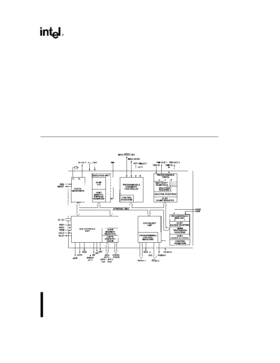
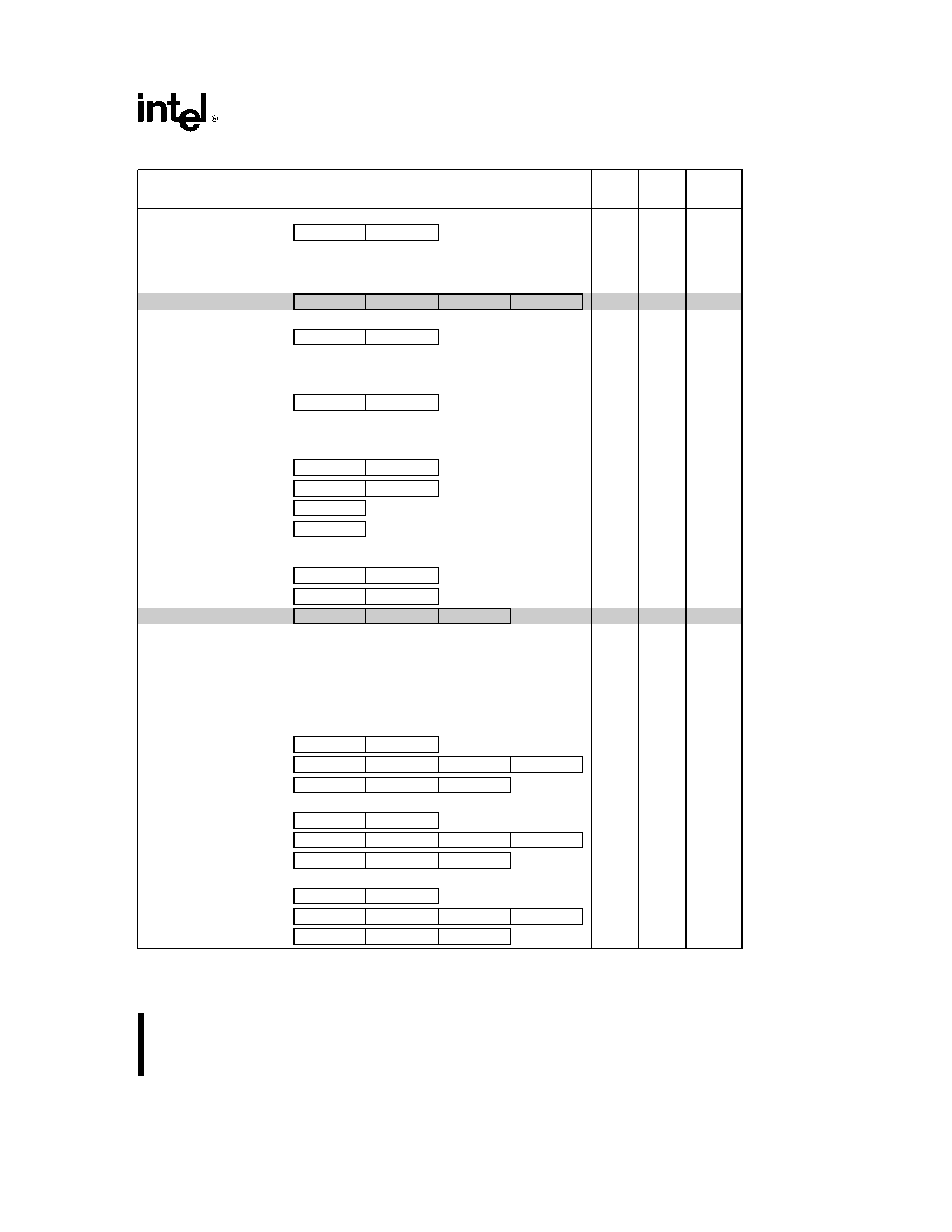
272430 � 1
Figure 1 Block Diagram
1

80186 80188 High-Integration 16-Bit Microprocessors
CONTENTS
PAGE
FUNCTIONAL DESCRIPTION
9
Introduction
9
CLOCK GENERATOR
9
Oscillator
9
Clock Generator
9
READY Synchronization
9
RESET Logic
9
LOCAL BUS CONTROLLER
9
Memory Peripheral Control
10
Local Bus Arbitration
10
Local Bus Controller and Reset
10
PERIPHERAL ARCHITECTURE
10
Chip-Select Ready Generation Logic
10
DMA Channels
11
Timers
11
Interrupt Controller
12
CONTENTS
PAGE
ABSOLUTE MAXIMUM RATINGS
15
D C CHARACTERISTICS
15
A C CHARACTERISTICS
16
EXPLANATION OF THE AC
SYMBOLS
18
WAVEFORMS
19
EXPRESS
25
EXECUTION TIMINGS
26
INSTRUCTION SET SUMMARY
27
FOOTNOTES
32
REVISION HISTORY
33
2
2

80186 80188
Contacts Facing Up
Contacts Facing Down
272430 � 2
Figure 2 Ceramic Leadless Chip Carrier (JEDEC Type A)
Pins Facing Up
Pins Facing Down
272430 � 3
Figure 3 Ceramic Pin Grid Array
NOTE
Pin names in parentheses apply to the 80188
3
3

80186 80188
Leads Facing Up
Leads Facing Down
272430 � 4
Figure 4 Plastic Leaded Chip Carrier
NOTE
Pin names in parentheses apply to the 80188
4
4

80186 80188
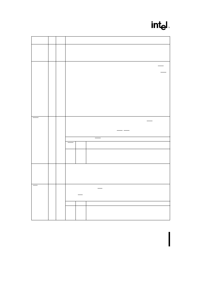
Table 1 Pin Descriptions
Symbol
Pin
Type
Name and Function
No
V
CC
9
I
SYSTEM POWER
a
5 volt power supply
43
V
SS
26
I
System Ground
60
RESET
57
O
Reset Output indicates that the CPU is being reset and can be used as a system
reset It is active HIGH synchronized with the processor clock and lasts an
integer number of clock periods corresponding to the length of the RES signal
X1
59
I
Crystal Inputs X1 and X2 provide external connections for a fundamental mode
parallel resonant crystal for the internal oscillator Instead of using a crystal an
X2
58
O
external clock may be applied to X1 while minimizing stray capacitance on X2
The input or oscillator frequency is internally divided by two to generate the
clock signal (CLKOUT)
CLKOUT
56
O
Clock Output provides the system with a 50% duty cycle waveform All device
pin timings are specified relative to CLKOUT
RES
24
I
An active RES causes the processor to immediately terminate its present
activity clear the internal logic and enter a dormant state This signal may be
asynchronous to the processor clock The processor begins fetching
instructions approximately 6
clock cycles after RES is returned HIGH For
proper initialization V
CC
must be within specifications and the clock signal must
be stable for more than 4 clocks with RES held LOW RES is internally
synchronized This input is provided with a Schmitt-trigger to facilitate power-on
RES generation via an RC network
TEST
47
I O
TEST is examined by the WAIT instruction If the TEST input is HIGH when
``WAIT'' execution begins instruction execution will suspend TEST will be
resampled until it goes LOW at which time execution will resume If interrupts
are enabled while the processor is waiting for TEST interrupts will be serviced
During power-up active RES is required to configure TEST as an input This pin
is synchronized internally
TMR IN 0
20
I
Timer Inputs are used either as clock or control signals depending upon the
programmed timer mode These inputs are active HIGH (or LOW-to-HIGH
TMR IN 1
21
I
transitions are counted) and internally synchronized
TMR OUT 0
22
O
Timer outputs are used to provide single pulse or continous waveform
generation depending upon the timer mode selected
TMR OUT 1
23
O
DRQ0
18
I
DMA Request is asserted HIGH by an external device when it is ready for DMA
Channel 0 or 1 to perform a transfer These signals are level-triggered and
DRQ1
19
I
internally synchronized
NMI
46
I
The Non-Maskable Interrupt input causes a Type 2 interrupt An NMI transition
from LOW to HIGH is latched and synchronized internally and initiates the
interrupt at the next instruction boundary NMI must be asserted for at least one
clock The Non-Maskable Interrupt cannot be avoided by programming
INT0
45
I
Maskable Interrupt Requests can be requested by activating one of these pins
When configured as inputs these pins are active HIGH Interrupt Requests are
INT1 SELECT
44
I
synchronized internally INT2 and INT3 may be configured to provide active-
INT2 INTA0
42
I O
LOW interrupt-acknowledge output signals All interrupt inputs may be
INT3 INTA1 IRQ
41
I O
configured to be either edge- or level-triggered To ensure recognition all
interrupt requests must remain active until the interrupt is acknowledged When
Slave Mode is selected the function of these pins changes (see Interrupt
Controller section of this data sheet)
NOTE
Pin names in parentheses apply to the 80188
5
5
80186 80188
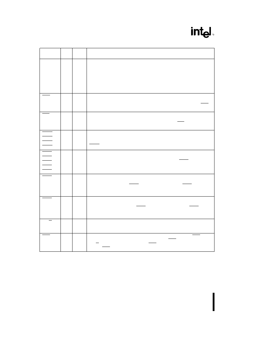
Table 1 Pin Descriptions
(Continued)
Symbol
Pin
Type
Name and Function
No
A19 S6
65
O
Address Bus Outputs (16�19) and Bus Cycle Status (3�6) indicate the four most
significant address bits during T
1
These signals are active HIGH During T
2
T
3
T
W
A18 S5
66
O
and T
4
the S6 pin is LOW to indicate a CPU-initiated bus cycle or HIGH to indicate a
A17 S4
67
O
DMA-initiated bus cycle During the same T-states S3 S4 and S5 are always LOW
A16 S3
68
O
The status pins float during bus HOLD or RESET
AD15 (A15)
1
I O
Address Data Bus signals constitute the time multiplexed memory or I O address (T
1
)
and data (T
2
T
3
T
W
and T
4
) bus The bus is active HIGH A
0
is analogous to BHE for
AD14 (A14)
3
I O
the lower byte of the data bus pins D
7
through D
0
It is LOW during T
1
when a byte is
AD13 (A13)
5
I O
to be transferred onto the lower portion of the bus in memory or I O operations BHE
AD12 (A12)
7
I O
does not exist on the 80188 as the data bus is only 8 bits wide
AD11 (A11)
10
I O
AD10 (A10)
12
I O
AD9 (A9)
14
I O
AD8 (A8)
16
I O
AD7
2
I O
AD6
4
I O
AD5
6
I O
AD4
8
I O
AD3
11
I O
AD2
13
I O
AD1
15
I O
AD0
17
I O
BHE S7
64
O
During T
1
the Bus High Enable signal should be used to determine if data is to be
enabled onto the most significant half of the data bus pins D
15
�D
8
BHE is LOW
(S7)
during T
1
for read write and interrupt acknowledge cycles when a byte is to be
transferred on the higher half of the bus The S
7
status information is available during
T
2
T
3
and T
4
S
7
is logically equivalent to BHE BHE S7 floats during HOLD On the
80188 S7 is high during normal operation
BHE and A0 Encodings (80186 Only)
BHE
A0
Function
Value
Value
0
0
Word Transfer
0
1
Byte Transfer on upper half of data bus (D15�D8)
1
0
Byte Transfer on lower half of data bus (D
7
�D
0
)
1
1
Reserved
ALE QS0
61
O
Address Latch Enable Queue Status 0 is provided by the processor to latch the
address ALE is active HIGH Addresses are guaranteed to be valid on the trailing
edge of ALE The ALE rising edge is generated off the rising edge of the CLKOUT
immediately preceding T
1
of the associated bus cycle effectively one-half clock cycle
earlier than in the 8086 The trailing edge is generated off the CLKOUT rising edge in
T
1
as in the 8086 Note that ALE is never floated
WR QS1
63
O
Write Strobe Queue Status 1 indicates that the data on the bus is to be written into a
memory or an I O device WR is active for T
2
T
3
and T
W
of any write cycle It is active
LOW and floats during HOLD When the processor is in queue status mode the ALE
QS0 and WR QS1 pins provide information about processor instruction queue
interaction
QS1
QS0
Queue Operation
0
0
No queue operation
0
1
First opcode byte fetched from the queue
1
1
Subsequent byte fetched from the queue
1
0
Empty the queue
NOTE
Pin names in parentheses apply to the 80188
6
6

80186 80188
Table 1 Pin Descriptions
(Continued)
Symbol
Pin
Type
Name and Function
No
RD QSMD
62
I O
Read Strobe is an active LOW signal which indicates that the processor is
performing a memory or I O read cycle It is guaranteed not to go LOW
before the A D bus is floated An internal pull-up ensures that RD is HIGH
during RESET Following RESET the pin is sampled to determine whether
the processor is to provide ALE RD and WR or queue status information
To enable Queue Status Mode RD must be connected to GND RD will
float during bus HOLD
ARDY
55
I
Asynchronous Ready informs the processor that the addressed memory
space or I O device will complete a data transfer The ARDY pin accepts a
rising edge that is asynchronous to CLKOUT and is active HIGH The
falling edge of ARDY must be synchronized to the processor clock
Connecting ARDY HIGH will always assert the ready condition to the CPU
If this line is unused it should be tied LOW to yield control to the SRDY pin
SRDY
49
I
Synchronous Ready informs the processor that the addressed memory
space or I O device will complete a data transfer The SRDY pin accepts an
active-HIGH input synchronized to CLKOUT The use of SRDY allows a
relaxed system timing over ARDY This is accomplished by elimination of
the one-half clock cycle required to internally synchronize the ARDY input
signal Connecting SRDY high will always assert the ready condition to the
CPU If this line is unused it should be tied LOW to yield control to the
ARDY pin
LOCK
48
O
LOCK output indicates that other system bus masters are not to gain
control of the system bus while LOCK is active LOW The LOCK signal is
requested by the LOCK prefix instruction and is activated at the beginning
of the first data cycle associated with the instruction following the LOCK
prefix It remains active until the completion of that instruction No
instruction prefetching will occur while LOCK is asserted When executing
more than one LOCK instruction always make sure there are 6 bytes of
code between the end of the first LOCK instruction and the start of the
second LOCK instruction LOCK is driven HIGH for one clock during RESET
and then floated
S0
52
O
Bus cycle status S0 � S2 are encoded to provide bus-transaction
information
S1
53
O
S2
54
O
Bus Cycle Status Information
S2
S1
S0
Bus Cycle Initiated
0
0
0
Interrupt Acknowledge
0
0
1
Read I O
0
1
0
Write I O
0
1
1
Halt
1
0
0
Instruction Fetch
1
0
1
Read Data from Memory
1
1
0
Write Data to Memory
1
1
1
Passive (no bus cycle)
The status pins float during HOLD
S2 may be used as a logical M IO indicator and S1 as a DT R indicator
NOTE
Pin names in parentheses apply to the 80188
7
7
80186 80188
Table 1 Pin Descriptions
(Continued)
Symbol
Pin
Type
Name and Function
No
HOLD
50
I
HOLD indicates that another bus master is requesting the local bus The
HOLD input is active HIGH HOLD may be asynchronous with respect to the
HLDA
51
O
processor clock The processor will issue a HLDA (HIGH) in response to a
HOLD request at the end of T
4
or T
i
Simultaneous with the issuance of
HLDA the processor will float the local bus and control lines After HOLD is
detected as being LOW the processor will lower HLDA When the processor
needs to run another bus cycle it will again drive the local bus and control
lines
UCS
34
O
Upper Memory Chip Select is an active LOW output whenever a memory
reference is made to the defined upper portion (1K � 256K block) of memory
This line is not floated during bus HOLD The address range activating UCS is
software programmable
LCS
33
O
Lower Memory Chip Select is active LOW whenever a memory reference is
made to the defined lower portion (1K � 256K) of memory This line is not
floated during bus HOLD The address range activating LCS is software
programmable
MCS0
38
O
Mid-Range Memory Chip Select signals are active LOW when a memory
reference is made to the defined mid-range portion of memory (8K � 512K)
MCS1
37
O
These lines are not floated during bus HOLD The address ranges activating
MCS2
36
O
MCS0 � 3 are software programmable
MCS3
35
O
PCS0
25
O
Peripheral Chip Select signals 0 � 4 are active LOW when a reference is made
to the defined peripheral area (64 Kbyte I O space) These lines are not
PCS1
27
O
floated during bus HOLD The address ranges activating PCS0 � 4 are
PCS2
28
O
software programmable
PCS3
29
O
PCS4
30
O
PCS5 A1
31
O
Peripheral Chip Select 5 or Latched A1 may be programmed to provide a
sixth peripheral chip select or to provide an internally latched A1 signal The
address range activating PCS5 is software-programmable PCS5 A1 does
not float during bus HOLD When programmed to provide latched A1 this pin
will retain the previously latched value during HOLD
PCS6 A2
32
O
Peripheral Chip Select 6 or Latched A2 may be programmed to provide a
seventh peripheral chip select or to provide an internally latched A2 signal
The address range activating PCS6 is software programmable PCS6 A2
does not float during bus HOLD When programmed to provide latched A2
this pin will retain the previously latched value during HOLD
DT R
40
O
Data Transmit Receive controls the direction of data flow through an
external data bus transceiver When LOW data is transferred to the
processsor When HIGH the processor places write data on the data bus
DEN
39
O
Data Enable is provided as a data bus transceiver output enable DEN is
active LOW during each memory and I O access DEN is HIGH whenever
DT R changes state During RESET DEN is driven HIGH for one clock then
floated DEN also floats during HOLD
NOTE
Pin names in parentheses apply to the 80188
8
8
80186 80188
FUNCTIONAL DESCRIPTION
Introduction
The following Functional Description describes the
base architecture of the 80186 The 80186 is a very
high integration 16-bit microprocessor It combines
15 � 20 of the most common microprocessor system
components onto one chip while providing twice the
performance of the standard 8086 The 80186 is ob-
ject code compatible with the 8086 8088 microproc-
essors and adds 10 new instruction types to the
8086 8088 instruction set
For more detailed information on the architecture
please refer to the 80C186XL 80C188XL User's
Manual The 80186 and the 80186XL devices are
functionally and register compatible
CLOCK GENERATOR
The processor provides an on-chip clock generator
for both internal and external clock generation The
clock generator features a crystal oscillator a divide-
by-two counter
synchronous and asynchronous
ready inputs and reset circuitry
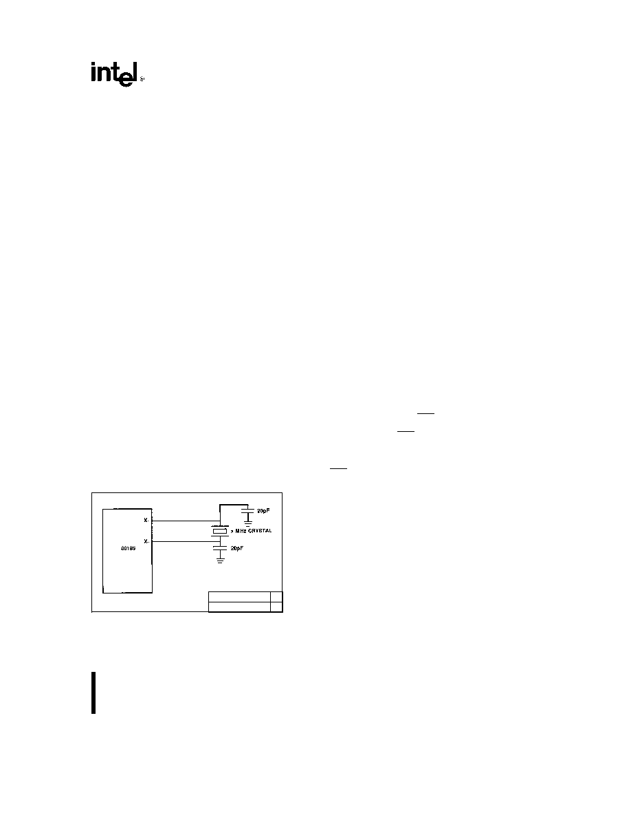
Oscillator
The oscillator circuit is designed to be used with a
parallel resonant fundamental mode crystal This is
used as the time base for the processor The crystal
frequency selected will be double the CPU clock fre-
quency Use of an LC or RC circuit is not recom-
mended with this oscillator If an external oscillator is
used it can be connected directly to the input pin X1
in lieu of a crystal The output of the oscillator is not
directly available outside the processor The recom-
mended crystal configuration is shown in Figure 5
x
80186-10 (10 MHz) 20
272430 � 5
80186
(8 MHz) 16
Figure 5 Recommended
Crystal Configuration
Intel recommends the following values for crystal se-
lection parameters
Temperature Range
0 to 70 C
ESR (Equivalent Series Resistance)
30X max
C
0
(Shunt Capacitance of Crystal)
7 0 pf max
C
1
(Load Capacitance)
20 pf
g
2 pf
Drive Level
1 mW max
Clock Generator
The clock generator provides the 50% duty cycle
processor clock for the processor It does this by
dividing the oscillator output by 2 forming the sym-
metrical clock If an external oscillator is used the
state of the clock generator will change on the fall-
ing edge of the oscillator signal The CLKOUT pin
provides the processor clock signal for use outside
the device This may be used to drive other system
components All timings are referenced to the output
clock
READY Synchronization
The processor provides both synchronous and asyn-
chronous ready inputs In addition the processor as
part of the integrated chip-select logic has the capa-
bility to program WAIT states for memory and
peripheral blocks
RESET Logic
The processor provides both a RES input pin and a
synchronized RESET output pin for use with other
system components The RES input pin is provided
with hysteresis in order to facilitate power-on Reset
generation via an RC network RESET output is
guaranteed to remain active for at least five clocks
given a RES input of at least six clocks
LOCAL BUS CONTROLLER
The processor provides a local bus controller to
generate the local bus control signals In addition it
employs a HOLD HLDA protocol for relinquishing
the local bus to other bus masters It also provides
outputs that can be used to enable external buffers
and to direct the flow of data on and off the local
bus
9
9

80186 80188
Memory Peripheral Control
The processor provides ALE RD and WR bus con-
trol signals The RD and WR signals are used to
strobe data from memory or I O to the processor or
to strobe data from the processor to memory or I O
The ALE line provides a strobe to latch the address
when it is valid The local bus controller does not
provide a memory I O signal If this is required use
the S2 signal (which will require external latching)
make the memory and I O spaces nonoverlapping
or use only the integrated chip-select circuitry
Local Bus Arbitration
The processor uses a HOLD HLDA system of local
bus exchange This provides an asynchronous bus
exchange mechanism This means multiple masters
utilizing the same bus can operate at separate clock
frequencies
The processor provides a single
HOLD HLDA pair through which all other bus mas-
ters may gain control of the local bus External cir-
cuitry must arbitrate which external device will gain
control of the bus when there is more than one alter-
nate local bus master When the processor relin-
quishes control of the local bus it floats DEN RD
WR
S0 � S2
LOCK
AD0 � AD15
(AD0 � AD7)
A16 � A19 (A8 � A19) BHE (S7) and DT R to allow
another master to drive these lines directly
Local Bus Controller and Reset
During RESET the local bus controller will perform
the following action
Drive DEN RD and WR HIGH for one clock cy-
cle then float
NOTE
RD is also provided with an internal pull-up de-
vice to prevent the processor from inadvertently
entering Queue Status Mode during RESET
Drive S0 � S2 to the inactive state (all HIGH) and
then float
Drive LOCK HIGH and then float
Float AD0 � 15 (AD0 � AD7) A16 � 19 (A8�A19)
BHE (S7) DT R
Drive ALE LOW (ALE is never floated)
Drive HLDA LOW
PERIPHERAL ARCHITECTURE
All of the integrated peripherals are controlled by
16-bit registers contained within an internal 256-byte
control block The control block may be mapped into
either memory or I O space Internal logic will recog-
nize control block addresses and respond to bus cy-
cles During bus cycles to internal registers the bus
controller will signal the operation externally (i e the
RD WR status address data etc lines will be driv-
en as in a normal bus cycle) but D
15�0
(D
7�0
)
SRDY and ARDY will be ignored The base address
of the control block must be on an even 256-byte
boundary (i e the lower 8 bits of the base address
are all zeros)
The control block base address is programmed by a
16-bit relocation register contained within the control
block at offset FEH from the base address of the
control block It provides the upper 12 bits of the
base address of the control block
In addition to providing relocation information for the
control block the relocation register contains bits
which place the interrupt controller into Slave Mode
and cause the CPU to interrupt upon encountering
ESC instructions
Chip-Select Ready Generation Logic
The
processor contains logic which provides
programmable chip-select generation for both mem-
ories and peripherals In addition it can be pro-
grammed to provide READY (or WAIT state) genera-
tion It can also provide latched address bits A1 and
A2 The chip-select lines are active for all memory
and I O cycles in their programmed areas whether
they be generated by the CPU or by the integrated
DMA unit
MEMORY CHIP SELECTS
The processor provides 6 memory chip select out-
puts for 3 address areas upper memory lower
memory and midrange memory One each is provid-
ed for upper memory and lower memory while four
are provided for midrange memory
UPPER MEMORY CS
The processor provides a chip select called UCS
for the top of memory The top of memory is usually
used as the system memory because after reset the
processor begins executing at memory location
FFFF0H
LOWER MEMORY CS
The processor provides a chip select for low memo-
ry called LCS The bottom of memory contains the
interrupt vector table starting at location 00000H
10
10

80186 80188
The lower limit of memory defined by this chip select
is always 0H while the upper limit is programmable
By programming the upper limit the size of the
memory block is defined
MID-RANGE MEMORY CS
The processor provides four MCS lines which are
active within a user-locatable memory block This
block can be located within the 1-Mbyte memory ad-
dress space exclusive of the areas defined by UCS
and LCS Both the base address and size of this
memory block are programmable
PERIPHERAL CHIP SELECTS
The processor can generate chip selects for up to
seven peripheral devices These chip selects are ac-
tive for seven contiguous blocks of 128 bytes above
a programmable base address The base address
may be located in either memory or I O space Sev-
en CS lines called PCS0 � 6 are generated by the
processor
PCS5 and PCS6 can also be pro-
grammed to provide latched address bits A1 and A2
If so programmed they cannot be used as peripher-
al selects These outputs can be connected directly
to the A0 and A1 pins used for selecting internal
registers of 8-bit peripheral chips
READY GENERATION LOGIC
The processor can generate a READY signal inter-
nally for each of the memory or peripheral CS lines
The number of WAIT states to be inserted for each
peripheral or memory is programmable to provide
0 � 3 wait states for all accesses to the area for
which the chip select is active In addition the proc-
essor may be programmed to either ignore external
READY for each chip-select range individually or to
factor external READY with the integrated ready
generator
CHIP SELECT READY LOGIC AND RESET
Upon RESET the Chip-Select Ready Logic will per-
form the following actions
All chip-select outputs will be driven HIGH
Upon leaving RESET the UCS line will be pro-
grammed to provide chip selects to a 1K block
with the accompanying READY control bits set at
011 to insert 3 wait states in conjunction with ex-
ternal READY (i e UMCS resets to FFFBH)
No other chip select or READY control registers
have any predefined values after RESET They
will not become active until the CPU accesses
their control registers Both the PACS and MPCS
registers must be accessed before the PCS lines
will become active
DMA Channels
The DMA controller provides two independent DMA
channels Data transfers can occur between memo-
ry and I O spaces (e g Memory to I O) or within the
same space (e g Memory to Memory or I O to I O)
Data can be transferred either in bytes or in words
(80186 only) to or from even or odd addresses
Each DMA channel maintains both a 20-bit source
and destination pointer which can be optionally in-
cremented or decremented after each data transfer
(by one or two depending on byte or word transfers)
Each data transfer consumes 2 bus cycles (a mini-
mum of 8 clocks) one cycle to fetch data and the
other to store data This provides a maximum data
transfer rate of 1 25 Mword sec or 2 5 Mbytes sec
at 10 MHz (half of this rate for the 80188)
DMA CHANNELS AND RESET
Upon RESET the DMA channels will perform the
following actions
The Start Stop bit for each channel will be reset
to STOP
Any transfer in progress is aborted
Timers
The processor provides three internal 16-bit pro-
grammable timers Two of these are highly flexible
and are connected to four external pins (2 per timer)
They can be used to count external events time ex-
ternal events generate nonrepetitive waveforms
etc The third timer is not connected to any external
pins and is useful for real-time coding and time de-
lay applications In addition the third timer can be
used as a prescaler to the other two or as a DMA
request source
11
11

80186 80188
TIMERS AND RESET
Upon RESET the Timers will perform the following
actions
All EN (Enable) bits are reset preventing timer
counting
For Timers 0 and 1 the RIU bits are reset to zero
and the ALT bits are set to one This results in the
Timer Out pins going high
Interrupt Controller
The processor can receive interrupts from a number
of sources both internal and external The internal
interrupt controller serves to merge these requests
on a priority basis for individual service by the CPU
Internal interrupt sources (Timers and DMA chan-
nels) can be disabled by their own control registers
or by mask bits within the interrupt controller The
interrupt controller has its own control register that
sets the mode of operation for the controller
INTERRUPT CONTROLLER AND RESET
Upon RESET the interrupt controller will perform
the following actions
All SFNM bits reset to 0 implying Fully Nested
Mode
All PR bits in the various control registers set to 1
This places all sources at lowest priority (level
111)
All LTM bits reset to 0 resulting in edge-sense
mode
All Interrupt Service bits reset to 0
All Interrupt Request bits reset to 0
All MSK (Interrupt Mask) bits set to 1 (mask)
All C (Cascade) bits reset to 0 (non-Cascade)
All PRM (Priority Mask) bits set to 1 implying no
levels masked
Initialized to Master Mode
12
12
80186 80188
272430 � 6
NOTE
Pin names in parenthesis apply to 80188
(1) BHE does not exist on the 80188 this is only required for a 16-bit data bus
Figure 6 Typical 80186 80188 Computer
13
13

80186 80188
272430 � 7
NOTE
Pin names in parentheses apply to 80188
(1) BHE does not exist on the 80188 this is only required for a 16-bit data bus
Figure 7 Typical 80186 80188 Multi-Master Bus Interface
14
14

80186 80188
ABSOLUTE MAXIMUM RATINGS
Ambient Temperature under Bias
0 C to 70 C
Storage Temperature
b
65 C to a150 C
Voltage on any Pin with
Respect to Ground
b
1 0V to a7V
Power Dissipation
3W
NOTICE This is a production data sheet The specifi-
cations are subject to change without notice
WARNING Stressing the device beyond the ``Absolute
Maximum Ratings'' may cause permanent damage
These are stress ratings only Operation beyond the
``Operating Conditions'' is not recommended and ex-
tended exposure beyond the ``Operating Conditions''
may affect device reliability
D C CHARACTERISTICS
(T
A
e
0 C to a70 C V
CC
e
5V
g
10%)
Applicable to 8 MHz and 10 MHz devices
Symbol
Parameter
Min
Max
Units
Test Conditions
V
IL
Input Low Voltage
b
0 5
a
0 8
V
V
IH
Input High Voltage
2 0
V
CC
a
0 5
V
(All except X1 and (RES)
V
IH1
Input High Voltage (RES)
3 0
V
CC
a
0 5
V
V
OL
Output Low Voltage
0 45
V
I
a
e
2 5 mA for S0 � S2
I
a
e
2 0 mA for all other Outputs
V
OH
Output High Voltage
2 4
V
I
oa
e b
400 mA
I
CC
Power Supply Current
600
mA
T
A
e b
40 C
550
mA
T
A
e
0 C
415
mA
T
A
e a
70 C
I
LI
Input Leakage Current
g
10
m
A
0V
k
V
IN
k
V
CC
I
LO
Output Leakage Current
g
10
m
A
0 45V
k
V
OUT
k
V
CC
V
CLO
Clock Output Low
0 6
V
I
a
e
4 0 mA
V
CHO
Clock Output High
4 0
V
I
oa
e b
200 mA
V
CLI
Clock Input Low Voltage
b
0 5
0 6
V
V
CHI
Clock Input High Voltage
3 9
V
CC
a
1 0
V
C
IN
Input Capacitance
10
pF
C
IO
I O Capacitance
20
pF
For extended temperature parts only
15
15
80186 80188
A C CHARACTERISTICS
(T
A
e
0 C to a70 C V
CC
e
5V
g
10%)
Timing Requirements
All Timings Measured At 1 5V Unless Otherwise Noted
Symbol
Parameter
8 MHz
10 MHz
Units
Conditions
Test
Min
Max
Min
Max
T
DVCL
Data in Setup (A D)
20
15
ns
T
CLDX
Data in Hold (A D)
10
8
ns
T
ARYHCH
Asynchronous Ready
20
15
ns
(ARDY) Active Setup
Time
(1)
T
ARYLCL
ARDY Inactive Setup Time
35
25
ns
T
CLARX
ARDY Hold Time
15
15
ns
T
ARYCHL
Asynchronous Ready
15
15
ns
Inactive Hold Time
T
SRYCL
Synchronous Ready (SRDY)
20
20
ns
Transition Setup Time
(2)
T
CLSRY
SRDY Transition Hold
15
15
ns
Time
(2)
T
HVCL
HOLD Setup
(1)
25
20
ns
T
INVCH
INTR NMI TEST TIM IN
25
25
ns
Setup
(1)
T
INVCL
DRQ0 DRQ1 Setup
(1)
25
20
ns
Master Interface Timing Responses
T
CLAV
Address Valid Delay
5
55
5
44
ns
C
L
e
20 pF�200 pF
all Outputs
T
CLAX
Address Hold
10
10
ns
(Except T
CLTMV
)
8 MHz and 10 MHz
T
CLAZ
Address Float Delay
T
CLAX
35
T
CLAX
30
ns
T
CHCZ
Command Lines Float Delay
45
40
ns
T
CHCV
Command Lines Valid Delay
55
45
ns
(after Float)
T
LHLL
ALE Width
T
CLCL
b
35
T
CLCL
b
30
ns
T
CHLH
ALE Active Delay
35
30
ns
T
CHLL
ALE Inactive Delay
35
30
ns
T
LLAX
Address Hold from ALE
T
CHCL
b
25
T
CHCL
b
20
ns
Inactive
T
CLDV
Data Valid Delay
10
44
10
40
ns
T
CLDOX
Data Hold Time
10
10
ns
T
WHDX
Data Hold after WR
T
CLCL
b
40
T
CLCL
b
34
ns
T
CVCTV
Control Active Delay 1
5
50
5
40
ns
T
CHCTV
Control Active Delay 2
10
55
10
44
ns
T
CVCTX
Control Inactive Delay
5
55
5
44
ns
T
CVDEX
DEN Inactive Delay
10
70
10
56
ns
(Non-Write Cycle)
1 To guarantee recognition at next clock
2 To guarantee proper operation
16
16
80186 80188
A C CHARACTERISTICS
(T
A
e
0 C to a70 C V
CC
e
5V
g
10%) (Continued)
Master Interface Timing Responses
(Continued)
Symbol
Parameter
8 MHz
10 MHz
Units
Conditions
Test
Min
Max
Min
Max
T
AZRL
Address Float to RD Active
0
0
ns
T
CLRL
RD Active Delay
10
70
10
56
ns
T
CLRH
RD Inactive Delay
10
55
10
44
ns
T
RHAV
RD Inactive to Address
T
CLCL
b
40
T
CLCL
b
40
ns
Active
T
CLHAV
HLDA Valid Delay
5
50
5
40
ns
T
RLRH
RD Width
2T
CLCL
b
50
2T
CLCL
b
46
ns
T
WLWH
WR Width
2T
CLCL
b
40
2T
CLCL
b
34
ns
T
AVLL
Address Valid to ALE Low
T
CLCH
b
25
T
CLCH
b
19
ns
T
CHSV
Status Active Delay
10
55
10
45
ns
T
CLSH
Status Inactive Delay
10
65
10
50
ns
T
CLTMV
Timer Output Delay
60
48
ns
100 pF max
8
10 MHz
T
CLRO
Reset Delay
60
48
ns
T
CHQSV
Queue Status Delay
35
28
ns
T
CHDX
Status Hold Time
10
10
ns
T
AVCH
Address Valid to Clock High
10
10
ns
T
CLLV
LOCK Valid Invalid Delay
5
65
5
60
ns
Chip-Select Timing Responses
T
CLCSV
Chip-Select Active Delay
66
45
ns
T
CXCSX
Chip-Select Hold from
35
35
ns
Command Inactive
T
CHCSX
Chip-Select Inactive Delay
5
35
5
32
ns
CLKIN Requirements
T
CKIN
CLKIN Period
62 5
250
50
250
ns
T
CKHL
CLKIN Fall Time
10
10
ns
3 5 to 1 0V
T
CKLH
CLKIN Rise Time
10
10
ns
1 0 to 3 5V
T
CLCK
CLKIN Low Time
25
20
ns
1 5V
T
CHCK
CLKIN High Time
25
20
ns
1 5V
CLKOUT Timing (200 pF load)
T
CICO
CLKIN to CLKOUT Skew
50
25
ns
T
CLCL
CLKOUT Period
125
500
100
500
ns
T
CLCH
CLKOUT Low Time
T
CLCL
b
7 5
T
CLCL
b
6 0
ns
1 5V
T
CHCL
CLKOUT High Time
T
CLCL
b
7 5
T
CLCL
b
6 0
ns
1 5V
T
CH1CH2
CLKOUT Rise Time
15
12
ns
1 0 to 3 5V
T
CL2CL1
CLKOUT Fall Time
15
12
ns
3 5 to 1 0V
17
17

80186 80188
EXPLANATION OF THE AC SYMBOLS
Each timing symbol has from 5 to 7 characters The
first character is always a ``T'' (stands for time) The
other characters
depending on their positions
stand for the name of a signal or the logical status of
that signal The following is a list of all the charac-
ters and what they stand for
A
Address
ARY Asynchronous Ready Input
C
Clock Output
CK
Clock Input
CS
Chip Select
CT
Control (DT R DEN
)
D
Data Input
DE
DEN
H
Logic Level High
IN
Input (DRQ0 TIM0
)
L
Logic Level Low or ALE
O
Output
QS
Queue Status (QS1 QS2)
R
RD signal RESET signal
S
Status (S0 S1 S2)
SRY Synchronous Ready Input
V
Valid
W
WR Signal
X
No Longer a Valid Logic Level
Z
Float
Examples
T
CLAV
Time from Clock low to Address valid
T
CHLH
Time from Clock high to ALE high
T
CLCSV
Time from Clock low to Chip Select valid
18
18

80186 80188
WAVEFORMS
MAJOR CYCLE TIMING
272430 � 8
NOTE
Pin names in parentheses apply to the 80188
19
19

80186 80188
WAVEFORMS
(Continued)
MAJOR CYCLE TIMING
(Continued)
NOTES
272430 � 9
1 INTA occurs one clock later in slave mode
2 Status inactive just prior to T
4
3 If latched A1 and A2 are selected instead of PCS5 and PCS6 only T
CLCSV
is applicable
4 Pin names in parentheses apply to the 80188
20
20

80186 80188
WAVEFORMS
(Continued)
272430 � 10
272430 � 11
272430 � 12
21
21

80186 80188
WAVEFORMS
(Continued)
272430 � 13
272430 � 14
22
22
80186 80188
WAVEFORMS
(Continued)
READY TIMING
272430 � 15
23
23

80186 80188
272430 � 16
NOTE
Pin names in parentheses apply to the 80188
24
24

80186 80188
WAVEFORMS
(Continued)
272430 � 17
EXPRESS
The Intel EXPRESS system offers enhancements to
the operational specifications of the microprocessor
EXPRESS products are designed to meet the needs
of those applications whose operating requirements
exceed commercial standards
The EXPRESS program includes the commercial
standard temperature range with burn-in and an ex-
tended temperature range without burn-in
With the commercial standard temperature range
operational characteristics are guaranteed over the
temperature range of 0 C to a70 C With the ex-
tended temperature range option operational char-
acteristics are guaranteed over the range of b40 C
to a85 C
The optional burn-in is dynamic for a minimum time
of 160 hours at a125 C with V
CC
e
5 5V
g
0 25V
following guidelines in MIL-STD-883 Method 1015
Package types and EXPRESS versions are identified
by a one- or two-letter prefix to the part number The
prefixes are listed in Table 2 All A C and D C speci-
fications not mentioned in this section are the same
for both commercial and EXPRESS parts
Table 2 Prefix Identification
Prefix
Package
Temperature
Burn-In
Type
Range
A
PGA
Commercial
No
N
PLCC
Commercial
No
R
LCC
Commercial
No
TA
PGA
Extended
No
QA
PGA
Commercial
Yes
QR
LCC
Commercial
Yes
NOTE
Not all package temperature range speed combinations
are available
25
25

80186 80188
EXECUTION TIMINGS
A determination of program execution timing must
consider the bus cycles necessary to prefetch in-
structions as well as the number of execution unit
cycles necessary to execute instructions The fol-
lowing instruction timings represent the minimum ex-
ecution time in clock cycles for each instruction The
timings given are based on the following assump-
tions
The opcode along with any data or displacement
required for execution of a particular instruction
has been prefetched and resides in the queue at
the time it is needed
No wait states or bus HOLDS occur
All word-data is located on even-address bound-
aries
All instructions which involve memory accesses can
also require one or two additional clocks above the
minimum timings shown due to the asynchronous
handshake between the bus interface unit (BIU) and
execution unit
All jumps and calls include the time required to fetch
the opcode of the next instruction at the destination
address
The 80186 has sufficient bus performance to ensure
that an adequate number of prefetched bytes will
reside in the queue (6 bytes) most of the time
Therefore actual program execution time will not be
substantially greater than that derived from adding
the instruction timings shown
The 80188 is noticeably limited in its performance
relative to the execution unit A sufficient number of
prefetched bytes may not reside in the prefetch
queue (4 bytes) much of the time Therefore actual
program execution time may be substantially greater
than that derived from adding the instruction timings
shown
26
26

80186 80188
INSTRUCTION SET SUMMARY
80186
80188
Function
Format
Clock
Clock
Comments
Cycles
Cycles
DATA TRANSFER
MOV
e
Move
Register to Register Memory
1 0 0 0 1 0 0 w
mod reg r m
2 12
2 12
Register memory to register
1 0 0 0 1 0 1 w
mod reg r m
2 9
2 9
Immediate to register memory
1 1 0 0 0 1 1 w
mod 000 r m
data
data if w
e
1
12 13
12 13
8 16-bit
Immediate to register
1 0 1 1 w reg
data
data if w
e
1
3 4
3 4
8 16-bit
Memory to accumulator
1 0 1 0 0 0 0 w
addr-low
addr-high
8
8
Accumulator to memory
1 0 1 0 0 0 1 w
addr-low
addr-high
9
9
Register memory to segment register
1 0 0 0 1 1 1 0
mod 0 reg r m
2 9
2 13
Segment register to register memory
1 0 0 0 1 1 0 0
mod 0 reg r m
2 11
2 15
PUSH
e
Push
Memory
1 1 1 1 1 1 1 1
mod 1 1 0 r m
16
20
Register
0 1 0 1 0 reg
10
14
Segment register
0 0 0 reg 1 1 0
9
13
Immediate
0 1 1 0 1 0 s 0
data
data if s
e
0
10
14
PUSHA
e
Push All
0 1 1 0 0 0 0 0
36
68
POP
e
Pop
Memory
1 0 0 0 1 1 1 1
mod 0 0 0 r m
20
24
Register
0 1 0 1 1 reg
10
14
Segment register
0 0 0 reg 1 1 1
(reg
i
01)
8
12
POPA
e
Pop All
0 1 1 0 0 0 0 1
51
83
XCHG
e
Exchange
Register memory with register
1 0 0 0 0 1 1 w
mod reg r m
4 17
4 17
Register with accumulator
1 0 0 1 0 reg
3
3
IN
e
Input from
Fixed port
1 1 1 0 0 1 0 w
port
10
10
Variable port
1 1 1 0 1 1 0 w
8
8
OUT
e
Output to
Fixed port
1 1 1 0 0 1 1 w
port
9
9
Variable port
1 1 1 0 1 1 1 w
7
7
XLAT
e
Translate byte to AL
1 1 0 1 0 1 1 1
11
15
LEA
e
Load EA to register
1 0 0 0 1 1 0 1
mod reg r m
6
6
LDS
e
Load pointer to DS
1 1 0 0 0 1 0 1
mod reg r m
(mod
i
11)
18
26
LES
e
Load pointer to ES
1 1 0 0 0 1 0 0
mod reg r m
(mod
i
11)
18
26
LAHF
e
Load AH with flags
1 0 0 1 1 1 1 1
2
2
SAHF
e
Store AH into flags
1 0 0 1 1 1 1 0
3
3
PUSHF
e
Push flags
1 0 0 1 1 1 0 0
9
13
POPF
e
Pop flags
1 0 0 1 1 1 0 1
8
12
Shaded areas indicate instructions not available in 8086 8088 microsystems
NOTE
Clock cycles shown for byte transfers for word operations add 4 clock cycles for each memory transfer
27
27

80186 80188
INSTRUCTION SET SUMMARY
(Continued)
80186
80188
Function
Format
Clock
Clock
Comments
Cycles
Cycles
DATA TRANSFER
(Continued)
SEGMENT
e
Segment Override
CS
0 0 1 0 1 1 1 0
2
2
SS
0 0 1 1 0 1 1 0
2
2
DS
0 0 1 1 1 1 1 0
2
2
ES
0 0 1 0 0 1 1 0
2
2
ARITHMETIC
ADD
e
Add
Reg memory with register to either
0 0 0 0 0 0 d w
mod reg r m
3 10
3 10
Immediate to register memory
1 0 0 0 0 0 s w
mod 0 0 0 r m
data
data if s w
e
01
4 16
4 16
Immediate to accumulator
0 0 0 0 0 1 0 w
data
data if w
e
1
3 4
3 4
8 16-bit
ADC
e
Add with carry
Reg memory with register to either
0 0 0 1 0 0 d w
mod reg r m
3 10
3 10
Immediate to register memory
1 0 0 0 0 0 s w
mod 0 1 0 r m
data
data if s w
e
01
4 16
4 16
Immediate to accumulator
0 0 0 1 0 1 0 w
data
data if w
e
1
3 4
3 4
8 16-bit
INC
e
Increment
Register memory
1 1 1 1 1 1 1 w
mod 0 0 0 r m
3 15
3 15
Register
0 1 0 0 0 reg
3
3
SUB
e
Subtract
Reg memory and register to either
0 0 1 0 1 0 d w
mod reg r m
3 10
3 10
Immediate from register memory
1 0 0 0 0 0 s w
mod 1 0 1 r m
data
data if s w
e
01
4 16
4 16
Immediate from accumulator
0 0 1 0 1 1 0 w
data
data if w
e
1
3 4
3 4
8 16-bit
SBB
e
Subtract with borrow
Reg memory and register to either
0 0 0 1 1 0 d w
mod reg r m
3 10
3 10
Immediate from register memory
1 0 0 0 0 0 s w
mod 0 1 1 r m
data
data if s w
e
01
4 16
4 16
Immediate from accumulator
0 0 0 1 1 1 0 w
data
data if w
e
1
3 4
3 4
8 16-bit
DEC
e
Decrement
Register memory
1 1 1 1 1 1 1 w
mod 0 0 1 r m
3 15
3 15
Register
0 1 0 0 1 reg
3
3
CMP
e
Compare
Register memory with register
0 0 1 1 1 0 1 w
mod reg r m
3 10
3 10
Register with register memory
0 0 1 1 1 0 0 w
mod reg r m
3 10
3 10
Immediate with register memory
1 0 0 0 0 0 s w
mod 1 1 1 r m
data
data if s w
e
01
3 10
3 10
Immediate with accumulator
0 0 1 1 1 1 0 w
data
data if w
e
1
3 4
3 4
8 16-bit
NEG
e
Change sign register memory
1 1 1 1 0 1 1 w
mod 0 1 1 r m
3 10
3 10
AAA
e
ASCII adjust for add
0 0 1 1 0 1 1 1
8
8
DAA
e
Decimal adjust for add
0 0 1 0 0 1 1 1
4
4
AAS
e
ASCII adjust for subtract
0 0 1 1 1 1 1 1
7
7
DAS
e
Decimal adjust for subtract
0 0 1 0 1 1 1 1
4
4
MUL
e
Multiply (unsigned)
1 1 1 1 0 1 1 w
mod 100 r m
Register-Byte
26�28
26�28
Register-Word
35�37
35�37
Memory-Byte
32�34
32�34
Memory-Word
41�43
41�43
Shaded areas indicate instructions not available in 8086 8088 microsystems
NOTE
Clock cycles shown for byte transfers for word operations add 4 clock cycles for each memory transfer
28
28
80186 80188
INSTRUCTION SET SUMMARY
(Continued)
80186
80188
Function
Format
Clock
Clock
Comments
Cycles
Cycles
ARITHMETIC
(Continued)
IMUL
e
Integer multiply (signed)
1 1 1 1 0 1 1 w
mod 1 0 1 r m
Register-Byte
25�28
25�28
Register-Word
34�37
34�37
Memory-Byte
31�34
31�34
Memory-Word
40�43
40�43
IMUL
e
Integer Immediate multiply
0 1 1 0 1 0 s 1
mod reg r m
data
data if s
e
0
22�25
22�25
(signed)
29�32
29�32
DIV
e
Divide (unsigned)
1 1 1 1 0 1 1 w
mod 1 1 0 r m
Register-Byte
29
29
Register-Word
38
38
Memory-Byte
35
35
Memory-Word
44
44
IDIV
e
Integer divide (signed)
1 1 1 1 0 1 1 w
mod 1 1 1 r m
Register-Byte
44�52
44�52
Register-Word
53�61
53�61
Memory-Byte
50�58
50�58
Memory-Word
59�67
59�67
AAM
e
ASCII adjust for multiply
1 1 0 1 0 1 0 0
0 0 0 0 1 0 1 0
19
19
AAD
e
ASCII adjust for divide
1 1 0 1 0 1 0 1
0 0 0 0 1 0 1 0
15
15
CBW
e
Convert byte to word
1 0 0 1 1 0 0 0
2
2
CWD
e
Convert word to double word
1 0 0 1 1 0 0 1
4
4
LOGIC
Shift Rotate Instructions
Register Memory by 1
1 1 0 1 0 0 0 w
mod TTT r m
2 15
2 15
Register Memory by CL
1 1 0 1 0 0 1 w
mod TTT r m
5
a
n 17
a
n 5
a
n 17
a
n
Register Memory by Count
1 1 0 0 0 0 0 w
mod TTT r m
count
5
a
n 17
a
n 5
a
n 17
a
n
TTT Instruction
0 0 0
ROL
0 0 1
ROR
0 1 0
RCL
0 1 1
RCR
1 0 0
SHL SAL
1 0 1
SHR
1 1 1
SAR
AND
e
And
Reg memory and register to either
0 0 1 0 0 0 d w
mod reg r m
3 10
3 10
Immediate to register memory
1 0 0 0 0 0 0 w
mod 1 0 0 r m
data
data if w
e
1
4 16
4 16
Immediate to accumulator
0 0 1 0 0 1 0 w
data
data if w
e
1
3 4
3 4
8 16-bit
TEST
e
And function to flags no result
Register memory and register
1 0 0 0 0 1 0 w
mod reg r m
3 10
3 10
Immediate data and register memory
1 1 1 1 0 1 1 w
mod 0 0 0 r m
data
data if w
e
1
4 10
4 10
Immediate data and accumulator
1 0 1 0 1 0 0 w
data
data if w
e
1
3 4
3 4
8 16-bit
OR
e
Or
Reg memory and register to either
0 0 0 0 1 0 d w
mod reg r m
3 10
3 10
Immediate to register memory
1 0 0 0 0 0 0 w
mod 0 0 1 r m
data
data if w
e
1
4 16
4 16
Immediate to accumulator
0 0 0 0 1 1 0 w
data
data if w
e
1
3 4
3 4
8 16-bit
Shaded areas indicate instructions not available in 8086 8088 microsystems
NOTE
Clock cycles shown for byte transfers for word operations add 4 clock cycles for each memory transfer
29
29

80186 80188
INSTRUCTION SET SUMMARY
(Continued)
80186
80188
Function
Format
Clock
Clock
Comments
Cycles
Cycles
LOGIC
(Continued)
XOR
e
Exclusive or
Reg memory and register to either
0 0 1 1 0 0 d w
mod reg r m
3 10
3 10
Immediate to register memory
1 0 0 0 0 0 0 w
mod 1 1 0 r m
data
data if w
e
1
4 16
4 16
Immediate to accumulator
0 0 1 1 0 1 0 w
data
data if w
e
1
3 4
3 4
8 16-bit
NOT
e
Invert register memory
1 1 1 1 0 1 1 w
mod 0 1 0 r m
3 10
3 10
STRING MANIPULATION
MOVS
e
Move byte word
1 0 1 0 0 1 0 w
14
14
CMPS
e
Compare byte word
1 0 1 0 0 1 1 w
22
22
SCAS
e
Scan byte word
1 0 1 0 1 1 1 w
15
15
LODS
e
Load byte wd to AL AX
1 0 1 0 1 1 0 w
12
12
STOS
e
Store byte wd from AL AX
1 0 1 0 1 0 1 w
10
10
INS
e
Input byte wd from DX port
0 1 1 0 1 1 0 w
14
14
OUTS
e
Output byte wd to DX port
0 1 1 0 1 1 1 w
14
14
Repeated by count in CX (REP REPE REPZ REPNE REPNZ)
MOVS
e
Move string
1 1 1 1 0 0 1 0
1 0 1 0 0 1 0 w
8
a
8n
8
a
8n
CMPS
e
Compare string
1 1 1 1 0 0 1 z
1 0 1 0 0 1 1 w
5
a
22n
5
a
22n
SCAS
e
Scan string
1 1 1 1 0 0 1 z
1 0 1 0 1 1 1 w
5
a
15n
5
a
15n
LODS
e
Load string
1 1 1 1 0 0 1 0
1 0 1 0 1 1 0 w
6
a
11n
6
a
11n
STOS
e
Store string
1 1 1 1 0 0 1 0
1 0 1 0 1 0 1 w
6
a
9n
6
a
9n
INS
e
Input string
1 1 1 1 0 0 1 0
0 1 1 0 1 1 0 w
8
a
8n
8
a
8n
OUTS
e
Output string
1 1 1 1 0 0 1 0
0 1 1 0 1 1 1 w
8
a
8n
8
a
8n
CONTROL TRANSFER
CALL
e
Call
Direct within segment
1 1 1 0 1 0 0 0
disp-low
disp-high
15
19
Register memory
1 1 1 1 1 1 1 1
mod 0 1 0 r m
13 19
17 27
indirect within segment
Direct intersegment
1 0 0 1 1 0 1 0
segment offset
23
31
segment selector
Indirect intersegment
1 1 1 1 1 1 1 1
mod 0 1 1 r m
(mod
i
11)
38
54
JMP
e
Unconditional jump
Short long
1 1 1 0 1 0 1 1
disp-low
14
14
Direct within segment
1 1 1 0 1 0 0 1
disp-low
disp-high
14
14
Register memory
1 1 1 1 1 1 1 1
mod 1 0 0 r m
11 17
11 21
indirect within segment
Direct intersegment
1 1 1 0 1 0 1 0
segment offset
14
14
segment selector
Indirect intersegment
1 1 1 1 1 1 1 1
mod 1 0 1 r m
(mod
i
11)
26
34
Shaded areas indicate instructions not available in 8086 8088 microsystems
NOTE
Clock cycles shown for byte transfers for word operations add 4 clock cycles for each memory transfer
30
30
80186 80188
INSTRUCTION SET SUMMARY
(Continued)
80186
80188
Function
Format
Clock
Clock
Comments
Cycles
Cycles
CONTROL TRANSFER
(Continued)
RET
e
Return from CALL
Within segment
1 1 0 0 0 0 1 1
16
20
Within seg adding immed to SP
1 1 0 0 0 0 1 0
data-low
data-high
18
22
Intersegment
1 1 0 0 1 0 1 1
22
30
Intersegment adding immediate to SP
1 1 0 0 1 0 1 0
data-low
data-high
25
33
JE JZ
e
Jump on equal zero
0 1 1 1 0 1 0 0
disp
4 13
4 13
JMP not
JL JNGE
e
Jump on less not greater or equal
0 1 1 1 1 1 0 0
disp
4 13
4 13
taken JMP
JLE JNG
e
Jump on less or equal not greater
0 1 1 1 1 1 1 0
disp
4 13
4 13
taken
JB JNAE
e
Jump on below not above or equal
0 1 1 1 0 0 1 0
disp
4 13
4 13
JBE JNA
e
Jump on below or equal not above
0 1 1 1 0 1 1 0
disp
4 13
4 13
JP JPE
e
Jump on parity parity even
0 1 1 1 1 0 1 0
disp
4 13
4 13
JO
e
Jump on overflow
0 1 1 1 0 0 0 0
disp
4 13
4 13
JS
e
Jump on sign
0 1 1 1 1 0 0 0
disp
4 13
4 13
JNE JNZ
e
Jump on not equal not zero
0 1 1 1 0 1 0 1
disp
4 13
4 13
JNL JGE
e
Jump on not less greater or equal
0 1 1 1 1 1 0 1
disp
4 13
4 13
JNLE JG
e
Jump on not less or equal greater
0 1 1 1 1 1 1 1
disp
4 13
4 13
JNB JAE
e
Jump on not below above or equal
0 1 1 1 0 0 1 1
disp
4 13
4 13
JNBE JA
e
Jump on not below or equal above
0 1 1 1 0 1 1 1
disp
4 13
4 13
JNP JPO
e
Jump on not par par odd
0 1 1 1 1 0 1 1
disp
4 13
4 13
JNO
e
Jump on not overflow
0 1 1 1 0 0 0 1
disp
4 13
4 13
JNS
e
Jump on not sign
0 1 1 1 1 0 0 1
disp
4 13
4 13
JCXZ
e
Jump on CX zero
1 1 1 0 0 0 1 1
disp
5 15
5 15
LOOP
e
Loop CX times
1 1 1 0 0 0 1 0
disp
6 16
6 16
LOOP not
LOOPZ LOOPE
e
Loop while zero equal
1 1 1 0 0 0 0 1
disp
6 16
6 16
taken LOOP
LOOPNZ LOOPNE
e
Loop while not zero equal
1 1 1 0 0 0 0 0
disp
6 16
6 16
taken
ENTER
e
Enter Procedure
1 1 0 0 1 0 0 0
data-low
data-high
L
L
e
0
15
19
L
e
1
25
29
L
l
1
22
a
16(n
b
1)
26
a
20(n
b
1)
LEAVE
e
Leave Procedure
1 1 0 0 1 0 0 1
8
8
INT
e
Interrupt
Type specified
1 1 0 0 1 1 0 1
type
47
47
Type 3
1 1 0 0 1 1 0 0
45
45
if INT taken
INTO
e
Interrupt on overflow
1 1 0 0 1 1 1 0
48 4
48 4
if INT not
taken
IRET
e
Interrupt return
1 1 0 0 1 1 1 1
28
28
BOUND
e
Detect value out of range
0 1 1 0 0 0 1 0
mod reg r m
33�35
33�35
Shaded areas indicate instructions not available in 8086 8088 microsystems
NOTE
Clock cycles shown for byte transfers for word operations add 4 clock cycles for each memory transfer
31
31

80186 80188
INSTRUCTION SET SUMMARY
(Continued)
80186
80188
Function
Format
Clock
Clock
Comments
Cycles
Cycles
PROCESSOR CONTROL
CLC
e
Clear carry
1 1 1 1 1 0 0 0
2
2
CMC
e
Complement carry
1 1 1 1 0 1 0 1
2
2
STC
e
Set carry
1 1 1 1 1 0 0 1
2
2
CLD
e
Clear direction
1 1 1 1 1 1 0 0
2
2
STD
e
Set direction
1 1 1 1 1 1 0 1
2
2
CLI
e
Clear interrupt
1 1 1 1 1 0 1 0
2
2
STI
e
Set interrupt
1 1 1 1 1 0 1 1
2
2
HLT
e
Halt
1 1 1 1 0 1 0 0
2
2
WAIT
e
Wait
1 0 0 1 1 0 1 1
6
6
if TEST
e
0
LOCK
e
Bus lock prefix
1 1 1 1 0 0 0 0
2
3
ESC
e
Processor Extension Escape
1 1 0 1 1 T T T
mod LLL r m
6
6
(TTT LLL are opcode to processor extension)
NOP
e
No Operation
1 0 0 1 0 0 0 0
3
3
Shaded areas indicate instructions not available in 8086 8088 microsystems
NOTE
Clock cycles shown for byte transfers for word operations add 4 clock cycles for each memory transfer
FOOTNOTES
The Effective Address (EA) of the memory operand
is computed according to the mod and r m fields
if mod e 11 then r m is treated as REG field
if mod e 00 then DISP e 0
disp-low and disp-high are absent
if mod e 01 then DISP e disp-low sign-extended to 16-bits disp-high
is absent
if mod e 10 then DISP e disp-high disp-low
if r m e 000 then EA e (BX) a (SI) a DISP
if r m e 001 then EA e (BX) a (DI) a DISP
if r m e 010 then EA e (BP) a (SI) a DISP
if r m e 011 then EA e (BP) a (DI) a DISP
if r m e 100 then EA e (SI) a DISP
if r m e 101 then EA e (DI) a DISP
if r m e 110 then EA e (BP) a DISP
if r m e 111 then EA e (BX) a DISP
DISP follows 2nd byte of instruction (before data if
required)
except if mod e 00 and r m e 110 then EA e
disp-high disp-low
EA calculation time is 4 clock cycles for all modes
and is included in the execution times given whenev-
er appropriate
Segment Override Prefix
0
0
1
reg
1
1
0
reg is assigned according to the following
reg
Segment
Register
00
ES
01
CS
10
SS
11
DS
REG is assigned according to the following table
16-Bit (w e 1)
8-Bit (w e 0)
000 AX
000 AL
001 CX
001 CL
010 DX
010 DL
011 BX
011 BL
100 SP
100 AH
101 BP
101 CH
110 SI
110 DH
111 DI
111 BH
The physical addresses of all operands addressed
by the BP register are computed using the SS seg-
ment register The physical addresses of the desti-
nation operands of the string primitive operations
(those addressed by the DI register) are computed
using the ES segment which may not be overridden
32
32

80186 80188
REVISION HISTORY
This data sheet replaces the following data sheets
210706-011 80188
210451-011 80186
33
33