November 1994
Order Number 210393-008
UPI-41AH 42AH
UNIVERSAL PERIPHERAL INTERFACE
8-BIT SLAVE MICROCONTROLLER
Y
UPI-41 6 MHz UPI-42 12 5 MHz
Y
Pin Software and Architecturally
Compatible with all UPI-41 and UPI-42
Products
Y
8-Bit CPU plus ROM OTP EPROM RAM
I O Timer Counter and Clock in a
Single Package
Y
2048 x 8 ROM OTP 256 x 8 RAM on
UPI-42 1024 x 8 ROM OTP 128 x 8
RAM on UPI-41 8-Bit Timer Counter 18
Programmable I O Pins
Y
One 8-Bit Status and Two Data
Registers for Asynchronous Slave-to-
Master Interface
Y
DMA Interrupt or Polled Operation
Supported
Y
Fully Compatible with all Intel and Most
Other Microprocessor Families
Y
Interchangeable ROM and OTP EPROM
Versions
Y
Expandable I O
Y
Sync Mode Available
Y
Over 90 Instructions 70% Single Byte
Y
Available in EXPRESS
Standard Temperature Range
Y
inteligent Programming Algorithm
Fast OTP Programming
Y
Available in 40-Lead Plastic and 44-
Lead Plastic Leaded Chip Carrier
Packages
(See Packaging Spec Order
240800-001)
Package Type P and N
The Intel UPI-41AH and UPI-42AH are general-purpose Universal Peripheral Interfaces that allow the designer
to develop customized solutions for peripheral device control
They are essentially ``slave'' microcontrollers or microcontrollers with a slave interface included on the chip
Interface registers are included to enable the UPI device to function as a slave peripheral controller in the MCS
Modules and iAPX family as well as other 8- 16- and 32-bit systems
To allow full user flexibility the program memory is available in ROM and One-Time Programmable EPROM
(OTP) All UPI-41AH and UPI-42AH devices are fully pin compatible for easy transition from prototype to
production level designs
210393 � 2
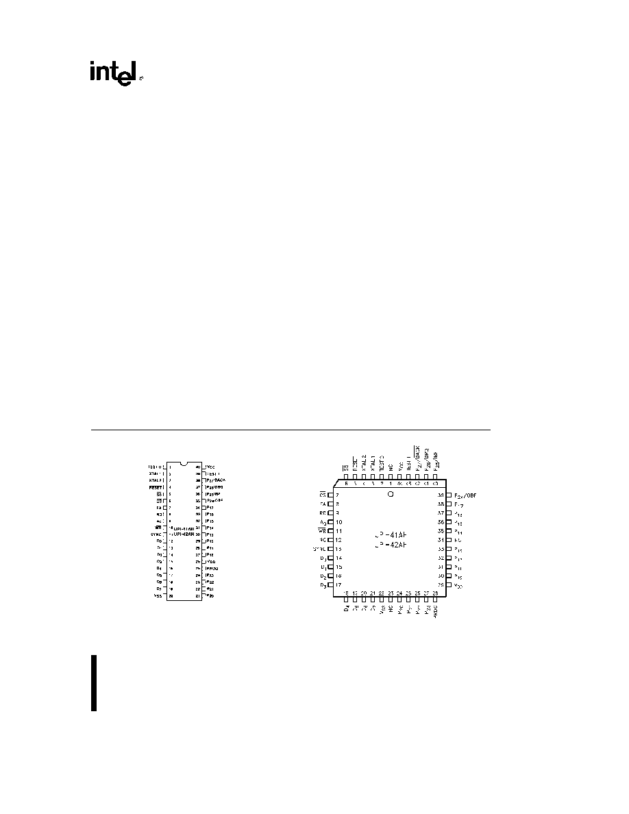
Figure 1 DIP Pin Configuration
210393 � 3
Figure 2 PLCC Pin Configuration

UPI-41AH 42AH
210393 � 1
Figure 3 Block Diagram
UPI PRODUCT MATRIX
UPI
ROM
OTP
RAM
Programming
Device
EPROM
Voltage
8042AH
2K
256
8242AH
2K
256
8742AH
2K
256
12 5V
8041AH
1K
128
8741AH
1K
128
12 5V
THE INTEL 8242
As shown in the UPI-42 product matrix the UPI-42
will be offered as a pre-programmed 8042 with sev-
eral software vendors' keyboard controller firmware
The current list of available 8242 versions include
keyboard controller firmware from both Phoenix
Technologies Ltd
IBM and Award Software Inc
The 8242 is programmed with Phoenix Technologies
Ltd keyboard controller firmware for AT-compatible
systems This keyboard controller is fully compatible
with all AT-compatible operating systems and appli-
cations The 8242PC also contains Phoenix Tech-
nologies Ltd
firmware
This keyboard controller
provides support for AT PS 2 and most EISA plat-
forms as well as PS 2-style mouse support for either
AT or PS 2 platforms
The Intel 8242BB is programmed with IBM's key-
board controller firmware The 8242BB provides an
off the shelf keyboard and auxiliary device controller
for AT PS 2 EISA and PCI architectures
The 8242WA contains Award Software Inc firm-
ware This device provides at AT-compatible key-
board controller for use in IBM PC AT compatible
computers
The 8242WB contains a version of
Award Software Inc firmware that provides PS 2
style mouse support in addition to the standard fea-
tures of the 8242WA
Contact factory for current code revision available in all versions of the 8242 product lines
2
UPI-41AH 42AH
Table 1 Pin Description
DIP
PLCC
Symbol
Pin
Pin
Type
Name and Function
No
No
TEST 0
1
2
I
TEST INPUTS
Input pins which can be directly tested using conditional branch
instructions
TEST 1
39
43
FREQUENCY REFERENCE
TEST 1 (T
1
) also functions as the event timer input (under
software control) TEST 0 (T
0
) is used during PROM programming and ROM EPROM
verification It is also used during Sync Mode to reset the instruction state to S1 and
synchronize the internal clock to PH1 See the Sync Mode Section
XTAL 1
2
3
I
INPUTS
Inputs for a crystal LC or an external timing signal to determine the internal
oscillator frequency
XTAL 2
3
4
RESET
4
5
I
RESET
Input used to reset status flip-flops and to set the program counter to zero
RESET is also used during EPROM programming and verification
SS
5
6
I
SINGLE STEP
Single step input used in conjunction with the SYNC output to step the
program through each instruction (EPROM) This should be tied to
a
5V when not used
This pin is also used to put the device in Sync Mode by applying 12 5V to it
CS
6
7
I
CHIP SELECT
Chip select input used to select one UPI microcomputer out of several
connected to a common data bus
EA
7
8
I
EXTERNAL ACCESS
External access input which allows emulation testing and
ROM EPROM verification This pin should be tied low if unused
RD
8
9
I
READ
I O read input which enables the master CPU to read data and status words from
the OUTPUT DATA BUS BUFFER or status register
A
0
9
10
I
COMMAND DATA SELECT
Address Input used by the master processor to indicate
whether byte transfer is data (A
0
e
0 F1 is reset) or command (A
0
e
1 F1 is set) A
0
e
0
during program and verify operations
WR
10
11
I
WRITE
I O write input which enables the master CPU to write data and command words
to the UPI INPUT DATA BUS BUFFER
SYNC
11
13
O
OUTPUT CLOCK
Output signal which occurs once per UPI instruction cycle SYNC can
be used as a strobe for external circuitry it is also used to synchronize single step
operation
D
0
� D
7
(BUS)
12 � 19 14 � 21
I O
DATA BUS
Three-state bidirectional DATA BUS BUFFER lines used to interface the UPI
microcomputer to an 8-bit master system data bus
P
10
� P
17
27 � 34 30 � 33
I O
PORT 1
8-bit PORT 1 quasi-bidirectional I O lines P
10
� P
17
access the signature row
and security bit
35 � 38
P
20
� P
27
21 � 24 24 � 27
I O
PORT 2
8-bit PORT 2 quasi-bidirectional I O lines The lower 4 bits (P
20
� P
23
) interface
directly to the 8243 I O expander device and contain address and data information during
35 � 38 39 � 42
PORT 4 � 7 access The upper 4 bits (P
24
� P
27
) can be programmed to provide interrupt
Request and DMA Handshake capability Software control can configure P
24
as Output
Buffer Full (OBF) interrupt P
25
as Input Buffer Full (IBF) interrupt P
26
as DMA Request
(DRQ) and P
27
as DMA ACKnowledge (DACK)
PROG
25
28
I O
PROGRAM
Multifunction pin used as the program pulse input during PROM programming
During I O expander access the PROG pin acts as an address data strobe to the 8243
This pin should be tied high if unused
V
CC
40
44
POWER
a
5V main power supply pin
V
DD
26
29
POWER
a
5V during normal operation
a
12 5V during programming operation Low
power standby supply pin
V
SS
20
22
GROUND
Circuit ground potential
3

UPI-41AH 42AH
UPI-41AH and UPI-42AH FEATURES
1
Two Data Bus Buffers one for input and one for
output This allows a much cleaner Master Slave
protocol
210393 � 4
2
8 Bits of Status
ST
7
ST
6
ST
5
ST
4
F
1
F
0
IBF OBF
D
7
D
6
D
5
D
4
D
3
D
2
D
1
D
0
ST
4
� ST
7
are user definable status bits These
bits are defined by the ``MOV STS A'' single byte
single cycle instruction Bits 4 � 7 of the acccumu-
lator are moved to bits 4 � 7 of the status register
Bits 0 � 3 of the status register are not affected
MOV STS A
Op Code 90H
1
0
0
1
0
0
0
0
D
7
D
0
3
RD and WR are edge triggered IBF OBF F
1
and
INT change internally after the trailing edge of RD
or WR
210393 � 6
During the time that the host CPU is reading the
status register the UPI is prevented from updat-
ing this register or is `locked out '
4
P
24
and P
25
are port pins or Buffer Flag pins
which can be used to interrupt a master proces-
sor These pins default to port pins on Reset
If the ``EN FLAGS'' instruction has been execut-
ed P
24
becomes the OBF (Output Buffer Full) pin
A ``1'' written to P
24
enables the OBF pin (the pin
outputs the OBF Status Bit) A ``0'' written to P
24
disables the OBF pin (the pin remains low) This
pin can be used to indicate that valid data is avail-
able from the UPI (in Output Data Bus Buffer)
If ``EN FLAGS'' has been executed P
25
becomes
the IBF (Input Buffer Full) pin A ``1'' written to P
25
enables the IBF pin (the pin outputs the inverse of
the IBF Status Bit A ``0'' written to P
25
disables
the IBF pin (the pin remains low) This pin can be
used to indicate that the UPI is ready for data
210393 � 5
Data Bus Buffer Interrupt Capability
EN FLAGS
Op Code 0F5H
1
1
1
1
0
1
0
1
D
7
D
0
4
UPI-41AH 42AH
5
P
26
and P
27
are port pins or DMA handshake pins
for use with a DMA controller These pins default
to port pins on Reset
If the ``EN DMA'' instruction has been executed
P
26
becomes the DRQ (DMA Request) pin A ``1''
written to P
26
causes a DMA request (DRQ is acti-
vated)
DRQ
is
deactivated
by
DACK
RD
DACK
WR or execution of the ``EN DMA'' in-
struction
If ``EN DMA'' has been executed P
27
becomes
the DACK (DMA ACKnowledge) pin This pin acts
as a chip select input for the Data Bus Buffer reg-
isters during DMA transfers
210393 � 7
DMA Handshake Capability
EN DMA
Op Code 0E5H
1
1
1
0
0
1
0
1
D
7
D
0
6
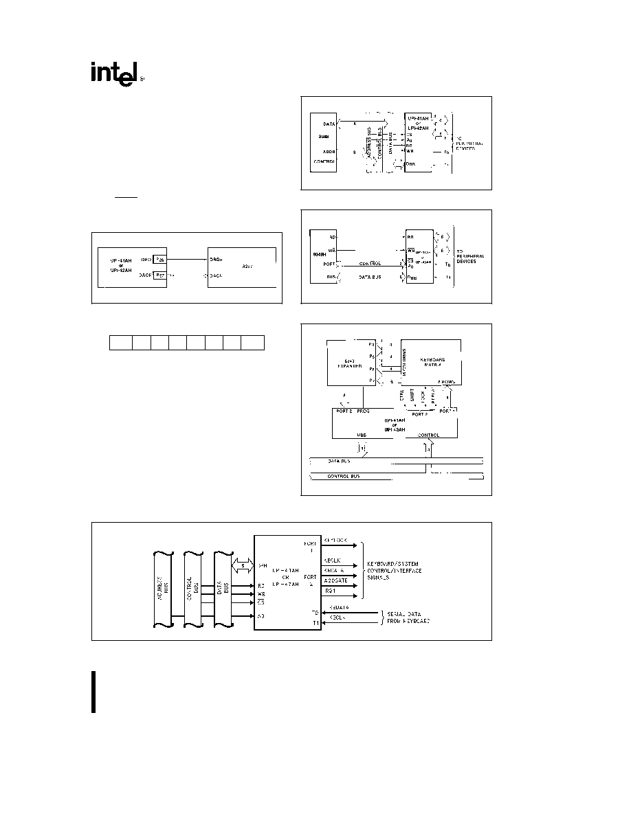
When EA is enabled on the UPI the program
counter is placed on Port 1 and the lower three
bits of Port 2 (MSB e P
22
LSB e P
10
) On the
UPI this information is multiplexed with PORT
DATA (see port timing diagrams at end of this
data sheet)
7
The 8741AH and 8742AH support the inteligent
Programming Algorithm (See the Programming
Section )
210393 � 8
Figure 5 8088-UPI-41AH 42AH Interface
210393 � 10
Figure 6 8048H-UPI-41 42 Interface
210393 � 9
Figure 7 UPI-41 42-8243 Keyboard Scanner
APPLICATIONS
210393 � 30
Figure 4 UPI-41AH 42AH Keyboard Controller
5

UPI-41AH 42AH
210393 � 11
Figure 8 UPI-41AH 42AH 80-Column
Matrix Printer Interface
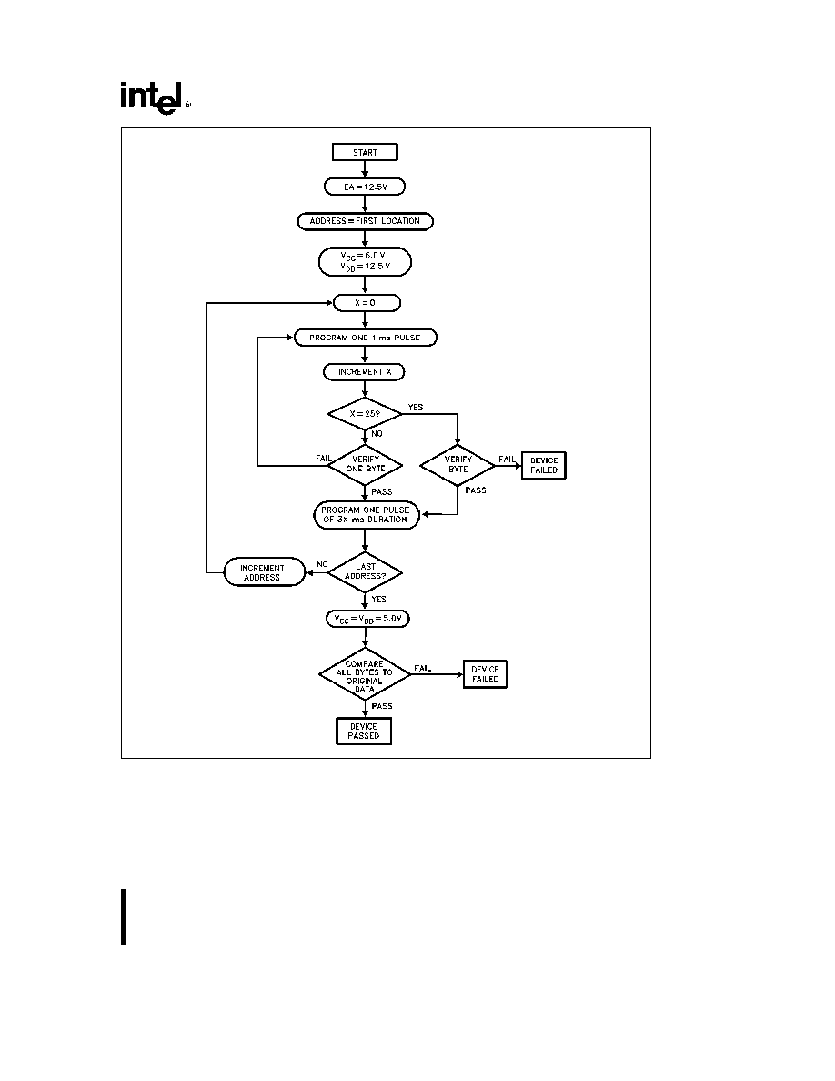
PROGRAMMING AND VERIFYING THE
8741AH AND 8742AH OTP EPROM
Programming Verification
In brief the programming process consists of acti-
vating the program mode applying an address
latching the address applying data and applying a
programming pulse Each word is programmed com-
pletely before moving on to the next and is followed
by a verification step The following is a list of the
pins used for programming and a description of their
functions
Pin
Function
XTAL 1
2 Clock Inputs
Reset
Initialization and Address Latching
Test 0
Selection of Program or Verify Mode
EA
Activation of Program Verify Signature
Row Security Bit Modes
BUS
Address and Data Input
Data Output During Verify
P
20�22
Address Input
V
DD
Programming Power Supply
PROG
Program Pulse Input
WARNING
An attempt to program a missocketed 8741AH or 8742AH will result in
severe damage to the part An indication of a properly socketed part is
the appearance of the SYNC clock output The lack of this clock may
be used to disable the programmer
The Program Verify sequence is
1 CS e 5V V
CC
e
5V V
DD
e
5V RESET e 0V
A
0
e
0V TEST 0 e 5V clock applied or internal
oscillator operating BUS floating PROG e 5V
2 Insert 8741AH or 8742AH in programming socket
3 TEST 0 e 0V (select program mode)
4 EA e 12 5V (active program mode)
5 V
CC
e
6V (programming supply)
6 V
DD
e
12 5V (programming power)
7 Address applied to BUS and P
20�22
8 RESET e 5V (latch address)
9 Data applied to BUS
10 PROG e 5V followed by one 1 ms pulse to 0V
11 TEST 0 e 5V (verify mode)
12 Read and verify data on BUS
13 TEST 0 e 0V
14 Apply overprogram pulse
15 RESET e 0V and repeat from step 6
16 Programmer should be at conditions of step 1
when 8741AH or 8742AH is removed from socket
Please follow the inteligent Programming flow chart
for proper programming procedure
inteligent Programming Algorithm
The inteligent Programming Algorithm rapidly pro-
grams Intel 8741AH 8742AH EPROMs using an effi-
cient and reliable method particularly suited to the
production programming environment Typical pro-
gramming time for individual devices is on the order
of 10 seconds Programming reliability is also en-
sured as the incremental program margin of each
byte is continually monitored to determine when it
has been successfully programmed A flowchart of
the 8741AH 8742AH inteligent Programming Algo-
rithm is shown in Figure 9
The inteligent Programming Algorithm utilizes two
different pulse types initial and overprogram The
duration of the initial PROG pulse(s) is one millisec-
ond which will then be followed by a longer overpro-
gram pulse of length 3X msec X is an iteration coun-
ter and is equal to the number of the initial one milli-
second pulses applied to a particular 8741AH
8742AH location before a correct verify occurs Up
to 25 one-millisecond pulses per byte are provided
for before the overprogram pulse is applied
6
UPI-41AH 42AH
210393 � 12
Figure 9 Programming Algorithm
7

UPI-41AH 42AH
The entire sequence of program pulses and byte
verifications is performed at V
CC
e
6 0V and V
DD
e
12 5V When the inteligent Programming cycle has
been completed all bytes should be compared to
the original data with V
CC
e
5 0 V
DD
e
5V
Verify
A verify should be performed on the programmed
bits to determine that they have been correctly pro-
grammed The verify is performed with T0 e 5V
V
DD
e
5V EA e 12 5V SS e 5V PROG e 5V
A0 e 0V and CS e 5V
SECURITY BIT
The security bit is a single EPROM cell outside the
EPROM array The user can program this bit with the
appropriate access code and the normal program-
ming procedure to inhibit any external access to the
EPROM contents Thus the user's resident program
is protected There is no direct external access to
this bit However the security byte in the signature
row has the same address and can be used to
check indirectly whether the security bit has been
programmed or not The security bit has no effect on
the signature mode so the security byte can always
be examined
SECURITY BIT PROGRAMMING
VERIFICATION
Programming
a Read the security byte of the signature mode
Make sure it is 00H
b Apply access code to appropriate inputs to put
the device into security mode
c Apply high voltage to EA and V
DD
pins
d Follow the programming procedure as per the
inteligent Programming Algorithm with known
data on the databus Not only the security bit but
also the security byte of the signature row is pro-
grammed
e Verify that the security byte of the signature
mode contains the same data as appeared on
the data bus (If DB0 � DB7 e high the security
byte will contain FFH )
f
Read two consecutive known bytes from the
EPROM array and verify that the wrong data are
retrieved in at least one verification
If the
EPROM can still be read the security bit may
have not been fully programmed though the se-
curity byte in the signature mode has
Verification
Since the security bit address overlaps the address
of the security byte of the signature mode it can be
used to check indirectly whether the security bit has
been programmed or not Therefore the security bit
verification is a mere read operation of the security
byte of the signature row (0FFH e security bit pro-
grammed 00H e security bit unprogrammed) Note
that during the security bit programming the reading
of the security byte does not necessarily indicate
that the security bit has been successfully pro-
grammed Thus it is recommended that two consec-
utive known bytes in the EPROM array be read and
the wrong data should be read at least once be-
cause it is highly improbable that random data coin-
cides with the correct ones twice
8
UPI-41AH 42AH
SIGNATURE MODE
The UPI-41AH 42AH has an additional 32 bytes of
EPROM available for Intel and user signatures and
miscellaneous purposes The 32 bytes are parti-
tioned as follows
A Test code checksum
This can accommodate
up to 25 bytes of code for testing the internal
nodes that are not testable by executing from the
external memory The test code checksum is
present on ROMs and OTPs
B Intel signature
This allows the programmer to
read from the UPI-41AH 42AH the manufacturer
of the device and the exact product name It fa-
cilitates automatic device identification and will
be present in the ROM and OTP versions Loca-
tion 10H contains the manufacturer code For In-
tel it is 89H Location 11H contains the device
code
The code is 43H and 42H for the 8042AH and
OTP 8742AH and 41H and 40H for the 8041AH
and OTP 8741AH respectively The code is 44H
for any device with the security bit set by Intel
C User signature
The user signature memory is
implemented in the EPROM and consists of 2
bytes for the customer to program his own signa-
ture code (for identification purposes and quick
sorting of previously programmed materials)
D Test signature
This memory is used to store
testing information such as test data bin num-
ber etc (for use in quality and manufacturing
control)
E Security byte
This byte is used to check
whether the security bit has been programmed
(see the security bit section)
The signature mode can be accessed by setting P10 e 0 P11 � P17 e 1 and then following the programming
and or verification procedures The location of the various address partitions are as follows
Address
Device
No of
Type
Bytes
Test Code Checksum
0
0FH
ROM OTP
25
16H
1EH
Intel Signature
10H
11H
ROM OTP
2
User Signature
12H
13H
OTP
2
Test Signature
14H
15H
ROM OTP
2
Security Byte
1FH
OTP
1
9
UPI-41AH 42AH
SYNC MODE
The Sync Mode is provided to ease the design of
multiple controller circuits by allowing the designer
to force the device into known phase and state time
The Sync Mode may also be utilized by automatic
test equipment (ATE) for quick easy and efficient
synchronizing between the tester and the DUT (de-
vice under test)
Sync Mode is enabled when SS pin is raised to high
voltage level of a12 volts To begin synchroniza-
tion T0 is raised to 5 volts at least four clock cycles
after SS T0 must be high for at least four X1 clock
cycles to fully reset the prescaler and time state
generators T0 may then be brought down during
low state of X1 Two clock cycles later with the ris-
ing edge of X1 the device enters into Time State 1
Phase 1 SS is then brought down to 5 volts 4 clocks
later after T0 RESET is allowed to go high 5 tCY (75
clocks) later for normal execution of code
SYNC MODE TIMING DIAGRAMS
210393 � 28
Minimum Specifications
SYNC Operation Time t
SYNC
e
3 5 XTAL 1 Clock cycles Reset Time t
RS
e
4 t
CY
NOTE
The rising and falling edges of T0 should occur during low state of XTAL1 clock
10

UPI-41AH 42AH
ACCESS CODE
The following table summarizes the access codes required to invoke the Sync Mode Signature Mode
and the Security Bit respectively Also the programming and verification modes are included for
comparison
Control Signals
Data Bus
Access Code
Modes
Port 2
Port 1
T0
RST SS EA PROG V
DD
V
CC
0
1
2
3
4
5
6
7
0 1 2 0
1 2 3 4 5 6 7
Programming
0
0
1 HV
1
V
DDH
V
CC
Address
Addr
a
0
a
1
X X X X X X
Mode
0
1
1 HV
STB
V
DDH
V
CC
Data In
Addr
Verification
0
0
1 HV
1
V
CC
V
CC
Address
Addr
a
0
a
1
X X X X X X
Mode
1
1
1 HV
1
V
CC
V
CC
Data Out
Addr
Sync Mode
STB
0
HV 0
X
V
CC
V
CC
X
X
X
X
X
X
X
X
X X X X X X X X X X X
High
Signature Prog
0
0
1 HV
1
V
DDH
V
CC
Addr (see Sig Mode Table)
0 0 0 0
1 1 1 1 X X 1
Mode
0
1
1 HV
STB
V
DDH
V
CC
Data In
0 0 0
Verify
0
0
1 HV
1
V
CC
V
CC
Addr (see Sig Mode Table)
0 0 0
1
1
1 HV
1
V
CC
V
CC
Data Out
0 0 0
Security
Prog
0
0
1 HV
1
V
DDH
V
CC
Address
0 0 0
Bit Byte
0
1
1 HV
STB
V
DDH
V
CC
Data In
0 0 0
Verify
0
0
1 HV
1
V
CC
V
CC
Address
0 0 0
1
1
1 HV
1
V
CC
V
CC
Data Out
0 0 0
NOTES
1 a
0
e
0 or 1 a
1
e
0 or 1 a
0
must
e
a
1
ABSOLUTE MAXIMUM RATINGS
Ambient Temperature Under Bias
0 C to a70 C
Storage Temperature
b
65 C to a150 C
Voltage on Any Pin with
Respect to Ground
b
0 5V to a7V
Power Dissipation
1 5 W
NOTICE This is a production data sheet The specifi-
cations are subject to change without notice
WARNING Stressing the device beyond the ``Absolute
Maximum Ratings'' may cause permanent damage
These are stress ratings only Operation beyond the
``Operating Conditions'' is not recommended and ex-
tended exposure beyond the ``Operating Conditions''
may affect device reliability
D C CHARACTERISTICS
T
A
e
0 C to a70 C V
CC
e
V
DD
e a
5V
g
10%
Symbol
Parameter
UPI-41AH 42AH
Units
Notes
Min
Max
V
IL
Input Low Voltage (Except XTAL1 XTAL2 RESET)
b
0 5
0 8
V
V
IL1
Input Low Voltage (XTAL1 XTAL2 RESET)
b
0 5
0 6
V
V
IH
Input High Voltage (Except XTAL1 XTAL2 RESET)
2 0
V
CC
V
V
IH1
Input High Voltage (XTAL1 RESET)
3 5
V
CC
V
V
IH2
Input High Voltage (XTAL2)
2 2
V
CC
V
V
OL
Output Low Voltage (D
0
� D
7
)
0 45
V
I
OL
e
2 0 mA
11
UPI-41AH 42AH
D C CHARACTERISTICS
T
A
e
0 C to a70 C V
CC
e
V
DD
e a
5V
g
10% (Continued)
Symbol
Parameter
UPI-41AH 42AH
Units
Notes
Min
Max
V
OL1
Output Low Voltage (P
10
P
17
P
20
P
27
Sync)
0 45
V
I
OL
e
1 6 mA
V
OL2
Output Low Voltage (PROG)
0 45
V
I
OL
e
1 0 mA
V
OH
Output High Voltage (D
0
� D
7
)
2 4
V
I
OH
e b
400 mA
V
OH1
Output High Voltage (All Other Outputs)
2 4
I
OH
e b
50 mA
I
IL
Input Leakage Current (T
0
T
1
RD WR CS A
0
EA)
g
10
m
A
V
SS
s
V
IN
s
V
CC
I
OFL
Output Leakage Current (D
0
� D
7
High Z State)
g
10
m
A
V
SS
a
0 45
s
V
OUT
s
V
CC
I
LI
Low Input Load Current (P
10
P
17
P
20
P
27
)
0 3
mA V
IL
e
0 8V
I
LI1
Low Input Load Current (RESET SS)
0 2
mA V
IL
e
0 8V
I
DD
V
DD
Supply Current
20
mA Typical e 8 mA
I
CC
a
I
DD
Total Supply Current
135
mA Typical e 80 mA
I
DD
Standby Power Down Supply Current
20
mA Typical e 8 mA
I
IH
Input Leakage Current (P
10
� P
17
P
20
� P
27
)
100
m
A
V
IN
e
V
CC
C
IN
Input Capacitance
10
pF
T
A
e
25 C
(1)
C
IO
I O Capacitance
20
pF
T
A
e
25 C
(1)
NOTE
1 Sampled not 100% tested
D C CHARACTERISTICS
PROGRAMMING
T
A
e
25 C
g
5 C V
CC
e
6V
g
0 25V V
DD
e
12 5V
g
0 5V
Symbol
Parameter
Min
Max
Units
V
DDH
V
DD
Program Voltage High Level
12
13
V
(1)
V
DDL
V
DD
Voltage Low Level
4 75
5 25
V
V
PH
PROG Program Voltage High Level
2 0
5 5
V
V
PL
PROG Voltage Low Level
b
0 5
0 8
V
V
EAH
Input High Voltage for EA
12 0
13 0
V
(2)
V
EAL
EA Voltage Low Level
b
0 5
5 25
V
I
DD
V
DD
High Voltage Supply Current
50 0
mA
I
EA
EA High Voltage Supply Current
1 0
mA
NOTES
1 Voltages over 13V applied to pin V
DD
will permanently damage the device
2 V
EAH
must be applied to EA before V
DDH
and removed after V
DDL
3 V
CC
must be applied simultaneously or before V
DD
and must be removed simultaneously or after V
DD
12
UPI-41AH 42AH
A C CHARACTERISTICS
T
A
e
0 C to a70 C V
SS
e
0V V
CC
e
V
DD
e a
5V
g
10%
DBB READ
Symbol
Parameter
Min
Max
Units
t
AR
CS A
0
Setup to RD
v
0
ns
t
RA
CS A
0
Hold After RD
u
0
ns
t
RR
RD Pulse Width
160
ns
t
AD
CS A
0
to Data Out Delay
130
ns
t
RD
RD
v
to Data Out Delay
0
130
ns
t
DF
RD
u
to Data Float Delay
85
ns
DBB WRITE
Symbol
Parameter
Min
Max
Units
t
AW
CS A
0
Setup to WR
v
0
ns
t
WA
CS A
0
Hold After WR
u
0
ns
t
WW
WR Pulse Width
160
ns
t
DW
Data Setup to WR
u
130
ns
t
WD
Data Hold After WR
u
0
ns
CLOCK
Symbol
Parameter
Min
Max
Units
t
CY
(UPI-41AH 42AH)
Cycle Time
1 2
9 20
m
s
(1)
t
CYC
(UPI-41AH 42AH)
Clock Period
80
613
ns
t
PWH
Clock High Time
30
ns
t
PWL
Clock Low Time
30
ns
t
R
Clock Rise Time
10
ns
t
F
Clock Fall Time
10
ns
NOTE
1 t
CY
e
15 f(XTAL)
A C CHARACTERISTICS
DMA
Symbol
Parameter
Min
Max
Units
t
ACC
DACK to WR or RD
0
ns
t
CAC
RD or WR to DACK
0
ns
t
ACD
DACK to Data Valid
DACK to Data Valid
0
130
ns
t
CRQ
RD or WR to DRQ Cleared
110
ns
(1)
NOTE
1 C
L
e
150 pF
13
UPI-41AH 42AH
A C CHARACTERISTICS
PROGRAMMING
T
A
e
25 C
g
5 C V
CC
e
6V
g
0 25V V
DDL
e a
5V
g
0 25V V
DDH
e
12 5V
g
0 5V
(8741AH 8742AH ONLY)
Symbol
Parameter
Min
Max
Units
t
AW
Address Setup Time to RESET
u
4t
CY
t
WA
Address Hold Time After RESET
u
4t
CY
t
DW
Data in Setup Time to PROG
v
4t
CY
t
WD
Data in Hold Time After PROG
u
4t
CY
t
PW
Initial Program Pulse Width
0 95
1 05
ms
(1)
t
TW
Test 0 Setup Time for Program Mode
4t
CY
t
WT
Test 0 Hold Time After Program Mode
4t
CY
t
DO
Test 0 to Data Out Delay
4t
CY
t
WW
RESET Pulse Width to Latch Address
4t
CY
t
r
t
f
PROG Rise and Fall Times
0 5
100
m
s
t
CY
CPU Operation Cycle Time
2 5
3 75
m
s
t
RE
RESET Setup Time Before EA
u
4t
CY
t
OPW
Overprogram Pulse Width
2 85
78 75
ms
(2)
t
DE
EA High to V
DD
High
1t
CY
NOTES
1 Typical Initial Program Pulse width tolerance
e
1 ms
g
5%
2 This variation is a function of the iteration counter value X
3 If TEST 0 is high t
DO
can be triggered by RESET
u
A C CHARACTERISTICS
PORT 2
T
A
e
0 C to a70 C V
CC
e a
5V
g
10%
Symbol
Parameter
f(t
CY
)
(3)
Min
Max
Units
t
CP
Port Control Setup Before Falling Edge of PROG
1 15 t
CY
b
28
55
ns
(1)
t
PC
Port Control Hold After Falling Edge of PROG
1 10 t
CY
125
ns
(2)
t
PR
PROG to Time P2 Input Must Be Valid
8 15 t
CY
b
16
650
ns
(1)
t
PF
Input Data Hold Time
0
150
ns
(2)
t
DP
Output Data Setup Time
2 10 t
CY
250
ns
(1)
t
PD
Output Data Hold Time
1 10 t
CY
b
80
45
ns
(2)
t
PP
PROG Pulse Width
6 10 t
CY
750
ns
NOTES
1 C
L
e
80 pF
2 C
L
e
20 pF
3 t
CY
e
1 25 ms
14

UPI-41AH 42AH
A C TESTING INPUT OUTPUT WAVEFORM
INPUT OUTPUT
210393 � 14
A C TESTING LOAD CIRCUIT
210393 � 15
DRIVING FROM EXTERNAL SOURCE-TWO OPTIONS
l
6 MHz
210393 � 16
210393 � 17
Rise and Fall Times Should Not Exceed 10 ns Resis-
tors to V
CC
are Needed to Ensure V
IH
e
3 5V if TTL
Circuitry is Used
LC OSCILLATOR MODE
L
C
NOMINAL
f e
1
2
q
0LC
45 H 20 pF
5 2 MHz
120 H 20 pF
3 2 MHz
C e
C a 3Cpp
2
Cpp j 5 � 10 pF
Pin-to-Pin Capacitance
210393 � 18
Each C Should be Approximately 20 pF including Stray Capacitance
CRYSTAL OSCILLATOR MODE
210393 � 19
C1
5 pF (STRAY 5 pF)
C2
(CRYSTAL a STRAY) 8 pF
C3
20 � 30 pF INCLUDING STRAY
Crystal Series Resistance Should
be Less Than 30X at 12 5 MHz
15
UPI-41AH 42AH
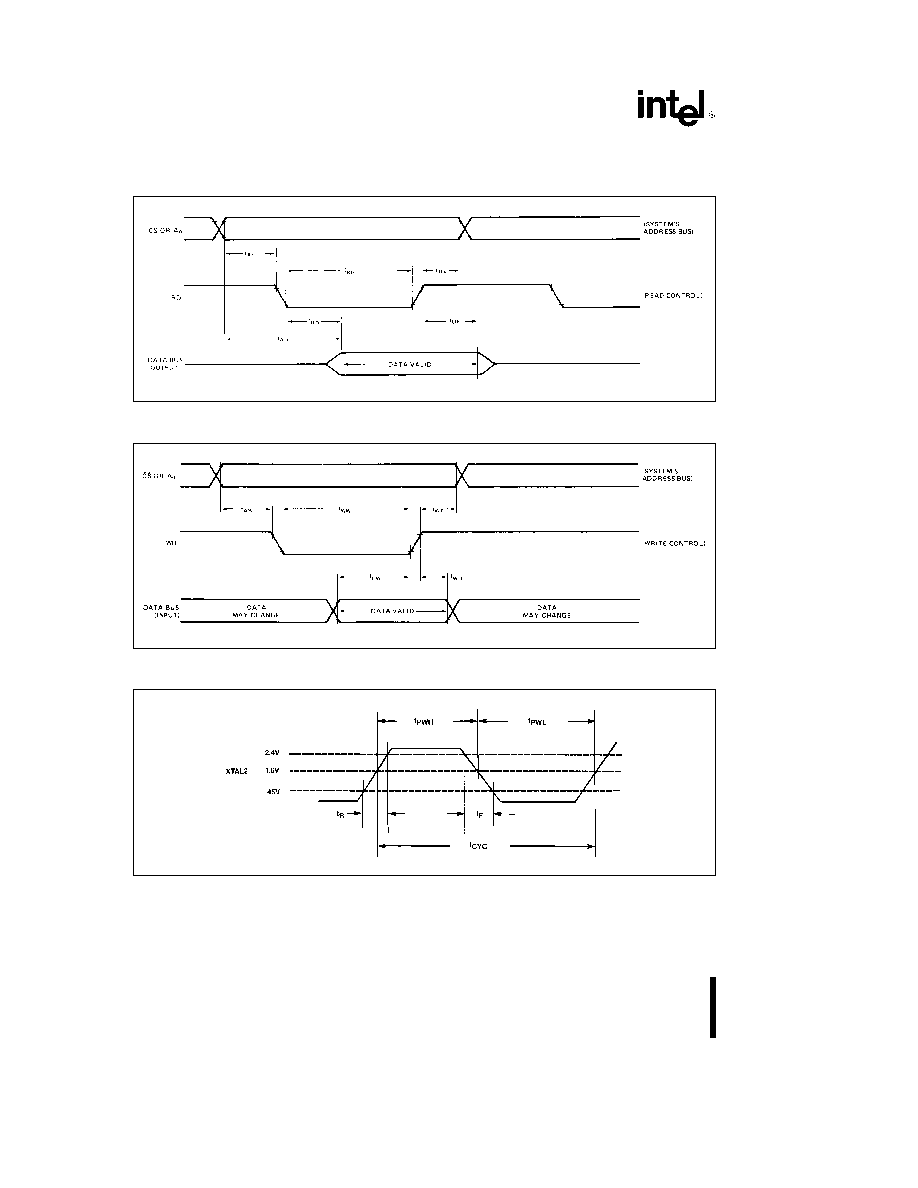
WAVEFORMS
READ OPERATION
DATA BUS BUFFER REGISTER
210393 � 20
WRITE OPERATION
DATA BUS BUFFER REGISTER
210393 � 21
CLOCK TIMING
210393 � 22
16

UPI-41AH 42AH
WAVEFORMS
(Continued)
COMBINATION PROGRAM VERIFY MODE
210393 � 23
NOTES
1 A
0
must be held low (0V) during program verify modes
2 For V
IH
V
IH1
V
IL
V
IL1
V
DDH
and V
DDL
please consult the D C Characteristics Table
3 When programming the 8741AH 8742AH a 0 1 mF capacitor is required across V
DD
and ground to suppress spurious
voltage transients which can damage the device
VERIFY MODE
210393 � 29
NOTES
1 PROG must float if EA is low
2 PROG must float or
e
5V when EA is high
3 P
10
� P
17
e
5V or must float
4 P
24
� P
27
e
5V or must float
5 A
0
must be held low during programming verify modes
17

UPI-41AH 42AH
WAVEFORMS
(Continued)
DMA
210393 � 25
PORT 2
210393 � 26
PORT TIMING DURING EXTERNAL ACCESS (EA)
210393 � 27
On the Rising Edge of SYNC and EA is Enabled Port Data is Valid and can be Strobed On the Trailing Edge of Sync
the Program Counter Contents are Available
18

UPI-41AH 42AH
Table 2 UPI Instruction Set
Mnemonic
Description
Bytes
Cycles
ACCUMULATOR
ADD A Rr
Add register to A
1
1
ADD A
Rr
Add data memory
1
1
to A
ADD A
data
Add immediate to A
2
2
ADDC A Rr
Add register to A
1
1
with carry
ADDC A
Rr
Add data memory
1
1
to A with carry
ADDC A
data
Add immediate
2
2
to A with carry
ANL A Rr
AND register to A
1
1
ANL A
Rr
AND data memory
1
1
to A
ANL A
data
AND immediate to A
2
2
ORL A Rr
OR register to A
1
1
ORL A
Rr
OR data memory
1
1
to A
ORL A
data
OR immediate to A
2
2
XRL A Rr
Exclusive OR regis-
1
1
ter to A
XRL A
Rr
Exclusive OR data
1
1
memory to A
XRL A
data
Exclusive OR imme-
2
2
diate to A
INC A
Increment A
1
1
DEC A
Decrement A
1
1
CLR A
Clear A
1
1
CPL A
Complement A
1
1
DA A
Decimal Adjust A
1
1
SWAP A
Swap nibbles of A
1
1
RL A
Rotate A left
1
1
RLC A
Rotate A left through
1
1
carry
RR A
Rotate A right
1
1
RRC A
Rotate A right
1
1
through carry
INPUT OUTPUT
IN A Pp
Input port to A
1
2
OUTL Pp A
Output A to port
1
2
ANL Pp
data
AND immediate to
2
2
port
ORL Pp
data
OR immediate to
2
2
port
IN A DBB
Input DBB to A
1
1
clear IBF
OUT DBB A
Output A to DBB
1
1
set OBF
MOV STS A
A
4
� A
7
to Bits 4 � 7 of
1
1
Status
MOVD A Pp
Input Expander
1
2
port to A
MOVD Pp A
Output A to
1
2
Expander port
ANLD Pp A
AND A to Expander
1
2
port
ORLD Pp A
OR A to Expander
1
2
port
Mnemonic
Description
Bytes
Cycles
DATA MOVES
MOV A Rr
Move register to A
1
1
MOV A
Rr
Move data memory
1
1
to A
MOV A
data
Move immediate to A
2
2
MOV Rr A
Move A to register
1
1
MOV
Rr A
Move A to data
1
1
memory
MOV Rr
data
Move immediate to
2
2
register
MOV
Rr
Move immediate to
2
2
data
data memory
MOV A PSW
Move PSW to A
1
1
MOV PSW A
Move A to PSW
1
1
XCH A Rr
Exchange A and
1
1
register
XCH A
Rr
Exchange A and
1
1
data memory
XCHD A
Rr
Exchange digit of A
1
1
and register
MOVP A
A
Move to A from
1
2
current page
MOVP3 A
A
Move to A from
1
2
page 3
TIMER COUNTER
MOV A T
Read Timer Counter
1
1
MOV T A
Load Timer Counter
1
1
STRT T
Start Timer
1
1
STRT CNT
Start Counter
1
1
STOP TCNT
Stop Timer Counter
1
1
EN TCNTI
Enable Timer
1
1
Counter Interrupt
DIS TCNTI
Disable Timer
1
1
Counter Interrupt
CONTROL
EN DMA
Enable DMA Hand-
1
1
shake Lines
EN I
Enable IBF Interrupt
1
1
DIS I
Diable IBF Inter-
1
1
rupt
EN FLAGS
Enable Master
1
1
Interrupts
SEL RB0
Select register
1
1
bank 0
SEL RB1
Select register
1
1
bank 1
NOP
No Operation
1
1
REGISTERS
INC Rr
Increment register
1
1
INC
Rr
Increment data
1
1
memory
DEC Rr
Decrement register
1
1
19

UPI-41AH 42AH
Table 2 UPI Instruction Set
(Continued)
Mnemonic
Description
Bytes
Cycles
SUBROUTINE
CALL addr
Jump to subroutine
2
2
RET
Return
1
2
RETR
Return and restore
1
2
status
FLAGS
CLR C
Clear Carry
1
1
CPL C
Complement Carry
1
1
CLR F0
Clear Flag 0
1
1
CPL F0
Complement Flag 0
1
1
CLR F1
Clear F1 Flag
1
1
CPL F1
Complement F1 Flag
1
1
BRANCH
JMP addr
Jump unconditional
2
2
JMPP
A
Jump indirect
1
2
DJNZ Rr addr
Decrement register
2
2
and jump
JC addr
Jump on Carry
e
1
2
2
JNC addr
Jump on Carry
e
0
2
2
JZ addr
Jump on A Zero
2
2
JNZ addr
Jump on A not Zero
2
2
JT0 addr
Jump on T0
e
1
2
2
JNT0 addr
Jump on T0
e
0
2
2
JT1 addr
Jump on T1
e
1
2
2
JNT1 addr
Jump on T1
e
0
2
2
JF0 addr
Jump on F0 Flag
e
1
2
2
JF1 addr
Jump on F1 Flag
e
1
2
2
JTF addr
Jump on Timer Flag
2
2
e
1 Clear Flag
JNIBF addr
Jump on IBF Flag
2
2
e
0
JOBF addr
Jump on OBF Flag
2
2
e
1
JBb addr
Jump on Accumula-
2
2
for Bit
INTEL CORPORATION 2200 Mission College Blvd Santa Clara CA 95052 Tel (408) 765-8080
INTEL CORPORATION (U K ) Ltd Swindon United Kingdom Tel (0793) 696 000
INTEL JAPAN k k Ibaraki-ken Tel 029747-8511
Printed in U S A xxxx 1196 B10M xx xx