Other brands and names are the property of their respective owners
Information in this document is provided in connection with Intel products Intel assumes no liability whatsoever including infringement of any patent or
copyright for sale and use of Intel products except as provided in Intel's Terms and Conditions of Sale for such products Intel retains the right to make
changes to these specifications at any time without notice Microcomputer Products may have minor variations to this specification known as errata
October 1989
COPYRIGHT
INTEL CORPORATION 1995
Order Number 270431-003
8XC152JA JB JC JD
UNIVERSAL COMMUNICATION CONTROLLER
8-BIT MICROCONTROLLER
X
8K Factory Mask Programmable ROM Available
Y
Superset of 80C51 Architecture
Y
Multi-Protocol Serial Communication
I O Port (2 048 Mbps 2 4 Mbps Max)
SDLC HDLC Only
CSMA CD and SDLC HDLC
User Definable Protocols
Y
Full Duplex Half Duplex
Y
MCS -51 Compatible UART
Y
16 5 MHz Maximum Clock Frequency
Y
Multiple Power Conservation Modes
Y
64KB Program Memory Addressing
Y
64KB Data Memory Addressing
Y
256 Bytes On-Chip RAM
Y
Dual On-Chip DMA Channels
Y
Hold Hold Acknowledge
Y
Two General Purpose Timer Counters
Y
5 or 7 I O Ports
Y
56 Special Function Registers
Y
11 Interrupt Sources
Y
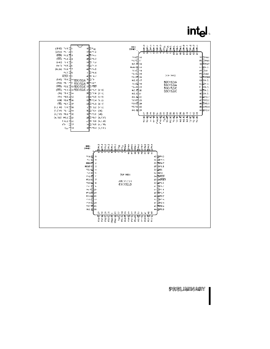
Available in 48 Pin Dual-in-Line Package
and 68 Pin Surface Mount PLCC
Package
(See Packaging Spec Order
231369)
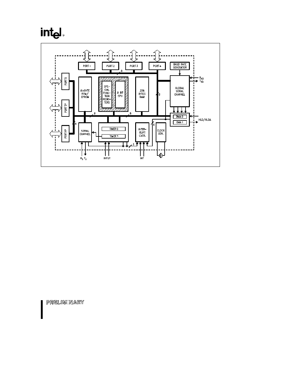
The 80C152 which is based on the MCS -51 CPU is a highly integrated single-chip 8-bit microcontroller
designed for cost-sensitive high-speed serial communications It is well suited for implementing Integrated
Services Digital Networks (ISDN) emerging Local Area Networks and user defined serial backplane applica-
tions In addition to the multi-protocol communication capability the 80C152 offers traditional microcontroller
features for peripheral I O interface and control
Silicon implementations are much more cost effective than multi-wire cables found in board level parallel-to-
serial and serial-to-parallel converters The 83C152 contains in silicon all the features needed for the serial-
to-parallel conversion Other 83C152 benefits include 1) better noise immunity through differential signaling or
fiber optic connections 2) data integrity utilizing the standard designed in CRC checks and 3) better modulari-
ty of hardware and software designs All of these
cost network parameter and real estate improvements
apply to 83C152 serial links between boards or systems and 83C152 serial links on a single board
8XC152JA JB JC JD
80C152JB JD General Description
The 80C152JB JD is a ROMless extension of the
80C152 Universal Communication controller The
80C152JB has the same five 8-bit I O ports of the
80C152 plus an additional two 8-bit I O ports Port 5
and Port 6 The 80C152JB JD also has two addi-
tional control pins EBEN (EPROM Bus ENable) and
EPSEN (EPROM bus Program Store ENable)
EBEN selects the functionality of Port 5 and Port 6
When EBEN is low these ports are strictly I O simi-
lar to Port 4 The SFR location for Port 5 is 91H and
Port 6 is 0A1H This means Port 5 and Port 6 are not
bit addressable With EBEN low all program memo-
ry fetches take place via Port 0 and Port 2 (The
80C152 is a ROMless only product) When EBEN is
high Port 5 and Port 6 form an address data bus
called the E-Bus (EPROM-Bus) for program memory
operations
EPSEN is used in conjunction with Port 5 and Port 6
program memory operations EPSEN functions like
PSEN during program memory operation but sup-
ports Port 5 and Port 6 EPSEN is the read strobe to
external program memory for Port 5 and Port 6
EPSEN is activated twice during each machine cycle
unless an external data memory operation occurs on
Port(s) 0 and Port 2 When external data memory is
accessed the second activation of EPSEN is
skipped which is the same as when using PSEN
Note that data memory fetches cannot be made
through Ports 5 and 6
When EBEN is high and EA is low all program mem-
ory operations take place via Ports 5 and 6 The high
byte of the address goes out on Port 6 and the low
byte is output on Port 5 ALE is still used to latch the
address on Port 5 Next the op code is read on Port
5 The timing is the same as when using Ports 0 and
2 for external program memory operations
Table 1 Program Memory Fetches
EBEN
EA
Program
PSEN
EPSEN
Comments
Fetch via
0
0
P0 P2
Active
Inactive
Addresses 0 � 0FFFFH
0
1
N A
N A
N A
Invalid Combination
1
0
P5 P6
Inactive
Active
Addresses 0 � 0FFFFH
1
1
P5 P6
Inactive
Active
Addresses 0 � 1FFFH
P0 P2
Active
Inactive
Addresses
t
2000H
Table 2 8XC152 Product Differences
ROMless
CSMA CD
HDLC SDLC
ROM
PLCC
PLCC
5 I O
7 I 0
Version
and
Only
Version
and
Only
Ports
Ports
HDLC SDLC
Available
DIP
80C152JA
(83C152JA)
80C152JB
80C152JC
(83C152JC)
80C152JD
NOTES
e
options available
0 standard frequency range 3 5 MHz to 12 MHz
0 ``
b
1'' frequency range 3 5 MHz to 16 5 MHz
4
8XC152JA JB JC JD
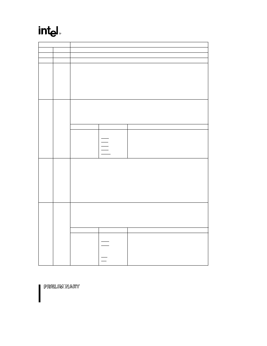
Pin
Pin Description
DIP
PLCC
(1)
48
2
V
CC
Supply voltage
24
3 33
(2)
V
SS
Circuit ground
18-21
27-30
Port 0
Port 0 is an 8-bit open drain bidirectional I O port As an output port each pin
25-28
34-37
can sink 8 LS TTL inputs Port 0 pins that have 1s written to them float and in that
state can be used as high-impedance inputs
Port 0 is also the multiplexed low-order address and data bus during accesses to
external program memory if EBEN is pulled low During accesses to external Data
Memory Port 0 always emits the low-order address byte and serves as the multiplexed
data bus In these applications it uses strong internal pullups when emitting 1s
Port 0 also outputs the code bytes during program verification External pullups are
required during program verification
1-8
4-11
Port 1
Port 1 is an 8-bit bidirectional I O port with internal pullups Port 1 pins that
have 1s written to them are pulled high by the internal pullups and in that state can be
used as inputs As inputs Port 1 pins that are externally being pulled low will source
current (I
IL
on the data sheet) because of the internal pullups
Port 1 also serves the functions of various special features of the 8XC152 as listed
below
Pin
Name
Alternate Function
P1 0
GRXD
GSC data input pin
P1 1
GTXD
GSC data output pin
P1 2
DEN
GSC enable signal for an external driver
P1 3
TXC
GSC input pin for external transmit clock
P1 4
RXC
GSC input pin for external receive clock
P1 5
HLD
DMA hold input output
P1 6
HLDA
DMA hold acknowledge input output
29-36
41-48
Port 2
Port 2 is an 8-bit bidirectional I O port with internal pullups Port 2 pins that
have 1s written to them are pulled high by the internal pullups and in that state can be
used as inputs As inputs Port 2 pins that are externally being pulled low will source
current (I
IL
on the data sheet) because of the internal pullups
Port 2 emits the high-order address byte during fetches from external Program
Memory if EBEN is pulled low During accesses to external Data Memory that use 16-
bit addresses (MOVX
DPTR and DMA operations) Port 2 emits the high-order
address byte In these applications it uses strong internal pullups when emitting 1s
During accesses to external Data Memory that use 8-bit addresses (MOVX
Ri)
Port 2 emits the contents of the P2 Special Function Register
Port 2 also receives the high-order address bits during program verification
10- 17
14-16
Port 3
Port 3 is an 8-bit bidirectional I O port with internal pullups Port 3 pins that
18 19
have 1s written to them are pulled high by the internal pullups and in that state can be
23-25
used as inputs As inputs Port 3 pins that are externally being pulled low will source
current (I
IL
on the data sheet) because of the pullups
Port 3 also serves the functions of various special features of the MCS-51 Family as
listed below
Pin
Name
Alternate Function
P3 0
RXD
Serial input line
P3 1
TXD
Serial output line
P3 2
INT0
External Interrupt 0
P3 3
INT1
External Interrupt 1
P3 4
T0
Timer 0 external input
P3 5
T1
Timer 1 external input
P3 6
WR
External Data Memory Write strobe
P3 7
RD
External Data Memory Read strobe
5