Document Outline
- 1.0. MICROPROCESSOR ARCHITECTURE OVERVIEW
- 2.0. PINOUT
- 3.0. ELECTRICAL SPECIFICATIONS
- 4.0. MECHANICAL SPECIFICATIONS
- 5.0. THERMAL SPECIFICATIONS
- 6.0. OverDrive ģ PROCESSOR SOCKET SPECIFICATION
- FIGURES
- TABLES
- Table 1. Pin Cross Reference by Pin Name
- Table 2. Quick Pin Reference
- Table 3. Bus Frequency Selections
- Table 4. Output Pins
- Table 5. Input Pins
- Table 6. Input/Output Pins
- Table 7. Inter-Processor Input/Output Pins
- Table 8. Pin Functional Grouping
- Table 9. 3.3V DC Specifications
- Table 10. 3.3V (5V-Safe) DC Specifications
- Table 11. Input and Output Characteristics
- Table 12. Power Dissipation Requirements for Thermal Solution Design
- Table 13. Pentium ģ Processor 75 and 100 MHz AC Specifications for 50-MHz Bus Operation
- Table 14. Pentium ģ Processor 75 and 100 MHz Dual Processor Mode AC Specifications for 50 MHz Bus Operation
- Table 15. Pentium ģ Processor 90, 120 and 150 MHz AC Specifications for 60-MHz Bus Operation
- Table 16. Pentium ģ Processor 90, 120 and 150 MHz Dual Processor Mode AC Specifications for 60-MHz Bus Operation
- Table 17. Pentium ģ Processor 100, 133, 166 and 200 MHz AC Specifications for 66-MHz Bus Operation
- Table 18. Pentium ģ Processor 100, 133, 166 and 200 MHz Dual Processor Mode AC Specifications for 66-MHz Bus Operation
- Table 19. Package Information Summary for Pentium Processor 75/90/100/120/133/150/166/200
- Table 20. SPGA Package Dimensions with Heat Spreader
- Table 21. SPGA Package Dimensions without Heat Spreader
- Table 22. PPGA Package Dimensions
- Table 23. Thermal Resistances for SPGA Packages with Heat Spreader
- Table 24. Thermal Resistances for SPGA Packages without Heat SpreaderĄ Pentium ģ Processor 75, 90, 100 and 120 MHz
- Table 25. Thermal Resistances for SPGA Packages without Heat SpreaderĄ Pentium ģ Processor 133, 150, 166 and 200 MHz
- Table 26. Thermal Resistances for PPGA Packages

E
June 1997
Order Number 241997-010
Max. Operating Frequency
75
MHz
90
MHz
100
MHz
120
MHz
133
MHz
150
MHz
166
MHz
200
MHz
iCOMP
ģ
Index 2.0 Rating
67
81
90
100
111
114
127
142
Note: Contact Intel Corporation for more information about iCOMP
ģ
Index 2.0 ratings.
n
Compatible with Large Software Base
MS-DOS*, Windows*, OS/2*, UNIX*
n
32-Bit CPU with 64-Bit Data Bus
n
Superscalar Architecture
Two Pipelined Integer Units Are Capable
of 2 Instructions/Clock
Pipe-lined Floating Point Unit
n
Separate Code and Data Caches
8-Kbyte Code, 8-Kbyte Write Back Data
MESI Cache Protocol
n
Advanced Design Features
Branch Prediction
Virtual Mode Extensions
n
3.3V BiCMOS Silicon Technology
n
4-Mbyte Pages for Increased TLB Hit Rate
n
IEEE 1149.1 Boundary Scan
n
Dual Processing Configuration
n
Functional Redundancy Checking Support
n
Internal Error Detection Features
n
Multi-Processor Support
Multiprocessor Instructions
Support for Second Level Cache
n
On-Chip Local APIC Controller
MP Interrupt Management
8259 Compatible
n
Upgradable with a Pentium
ģ
OverDrive
ģ
Processor
n
Power Management Features
System Management Mode
Clock Control
n
Fractional Bus Operation
200-MHz Core/66-MHz Bus
166-MHz Core/66-MHz Bus
150-MHz Core/60-MHz Bus
133-MHz Core/66-MHz Bus
120-MHz Core/60-MHz Bus
100-MHz Core/66-MHz Bus
100-MHz Core/50-MHz Bus
90-MHz Core/60-MHz Bus
75-MHz Core/50-MHz Bus
The Pentium
ģ
processor 75/90/100/120/133/150/166/200 extends the Pentium processor family, providing
performance needed for mainstream desktop applications as well as for workstations and servers. The Pentium
processor is compatible with the entire installed base of applications for DOS*, Windows*, OS/2*, and UNIX*.
The Pentium processor 75/90/100/120/133/150/166/200 superscalar architecture can execute two instructions
per clock cycle. Branch prediction and separate caches also increase performance. The pipelined floating point
unit delivers workstation level performance. Separate code and data caches reduce cache conflicts while
remaining software transparent. The Pentium processor 75/90/100/120/133/150/166/200 has 3.3 million
transistors and is built on Intel's advanced 3.3V BiCMOS silicon technology. The Pentium processor
75/90/100/120/133/150/166/200 has on-chip dual processing support, a local multiprocessor interrupt controller,
and SL power management features. The Pentium processor may contain design defects or errors known as
errata which may cause the product to deviate from published specifications. Current characterized errata are
available upon request.
PENTIUM
ģ
PROCESSOR

CONTENTS
PAGE
PAGE
1.0. MICROPROCESSOR ARCHITECTURE
OVERVIEW ....................................................... 3
1.1. Pentiumģ Processor Family Architecture...... 3
1.2. Pentiumģ Processor
75/90/100/120/133/150/166/200.................... 6
2.0. PINOUT.............................................................. 8
2.1. Pinout and Pin Descriptions........................... 8
2.2. Design Notes................................................ 12
2.3. Quick Pin Reference.................................... 12
2.4. Pin Reference Tables................................... 22
2.5. Pin Grouping According to Function............ 26
3.0. ELECTRICAL SPECIFICATIONS .................. 27
3.1. Electrical Differences Between Pentiumģ
Processor 75/90/100/120/133/150/166/200
and Pentium Processor 60/66...................... 27
3.2. Absolute Maximum Ratings..........................28
3.3. DC Specifications.........................................28
3.4. AC Specifications.........................................31
4.0. MECHANICAL SPECIFICATIONS .................56
5.0. THERMAL SPECIFICATIONS........................62
5.1. Measuring Thermal Values..........................62
6.0. OverDriveģ PROCESSOR SOCKET
SPECIFICATION .............................................69
6.1. Introduction...................................................69
6.2. Socket 5 .......................................................69
6.3. Socket 7 .......................................................70
Information in this document is provided in connection with Intel products. No license, express or implied, by estoppel or
otherwise, to any intellectual property rights is granted by this document. Except as provided in Intel's Terms and Conditions of
Sale for such products, Intel assumes no liability whatsoever, and Intel disclaims any express or implied warranty, relating to
sale and/or use of Intel products including liability or warranties relating to fitness for a particular purpose, merchantability, or
infringement of any patent, copyright or other intellectual property right. Intel products are not intended for use in medical, life
saving, or life sustaining applications.
Intel may make changes to specifications and product descriptions at any time, without notice.
Designers must not rely on the absence or characteristics of any features or instructions marked "reserved" or "undefined."
Intel reserves these for future definition and shall have no responsibility whatsoever for conflicts or incompatibilities arising from
future changes to them.
The Pentium
ģ
processor may contain design defects or errors known as errata which may cause the product to deviate from
published specifications. Current characterized errata are available on request.
Contact your local Intel sales office or your distributor to obtain the latest specifications and before placing your product order.
Copies of documents which have an ordering number and are referenced in this document, or other Intel literature, may be
obtained from:
Intel Corporation
P.O. Box 7641
Mt. Prospect IL 60056-7641
or call 1-800-879-4683
or visit Intel's website at http:\\www.intel.com
Copyright © Intel Corporation 1993, 1996, 1997.
* Third-party brands and names are the property of their respective owners.

E
PENTIUMģ PROCESSOR 75/90/100/120/133/150/166/200
3
1.0.
MICROPROCESSOR
ARCHITECTURE OVERVIEW
The Pentium
ģ
processor 75/90/100/120/133/
150/166/200 extends the Intel Pentium family of
microprocessors. It is binary compatible with the
8086/88, 80286, Intel386TM DX CPU, Intel386 SX
CPU, Intel486TM DX CPU, Intel486 SX CPU,
Intel486 DX2 CPU, and Pentium processor 60/66.
The Pentium processor family consists of the
following products.
∑
Described in this document (product code
80502). The name "Pentium processor
75/90/100/120/133/150/166/200" will be used to
refer to these products:
≠
Pentium processor at 200 MHz, iCOMP
ģ
Index 2.0 rating = 142
≠
Pentium processor at 166 MHz, iCOMP
Index 2.0 rating = 127
≠
Pentium processor at 150 MHz, iCOMP
Index 2.0 rating = 114
≠
Pentium processor at 133 MHz, iCOMP
Index 2.0 rating = 111
≠
Pentium processor at 120 MHz, iCOMP
Index 2.0 rating = 100
≠
Pentium processor at 100 MHz, iCOMP
Index 2.0 rating = 90
≠
Pentium processor at 90 MHz, iCOMP
Index 2.0 rating = 81
≠
Pentium processor at 75 MHz, iCOMP
Index 2.0 rating = 67
∑
Original Pentium processor. The name
"Pentium processor 60/66" will be used to refer
to the original 60 and 66 MHz version products:
≠
Pentium processor at 66 MHz, iCOMP
Index 2.0 rating = 57
≠
Pentium processor at 60 MHz, iCOMP
Index 2.0 rating = 51
The Pentium processor family architecture contains
all of the features of the Intel486 CPU family, and
provides significant enhancements and additions
including the following:
∑
Superscalar Architecture
∑
Dynamic Branch Prediction
∑
Pipelined Floating-Point Unit
∑
Improved Instruction Execution Time
∑
Separate 8K Code and 8K Data Caches
∑
Writeback MESI Protocol in the Data Cache
∑
64-Bit Data Bus
∑
Bus Cycle Pipelining
∑
Address Parity
∑
Internal Parity Checking
∑
Functional Redundancy Checking
∑
Execution Tracing
∑
Performance Monitoring
∑
IEEE 1149.1 Boundary Scan
∑
System Management Mode
∑
Virtual Mode Extensions
In addition to the features listed above, the Pentium
processor 75/90/100/120/133/150/166/200 offers
the following enhancements over Pentium
processor 60/66:
∑
Fractional bus operation allowing higher core
frequency operation
∑
Dual processing support
∑
SL power management features
∑
On-chip local APIC device
1.1.
Pentium
ģ
Processor Family
Architecture
The application instruction set of the Pentium
processor family includes the complete Intel486
CPU family instruction set with extensions to
accommodate some of the additional functionality of
the Pentium processors. All application software
written for the Intel386 and Intel486 family
microprocessors will run on the Pentium processors
without modification. The on-chip memory
management unit (MMU) is completely compatible
with the Intel386 family and Intel486 family of CPUs.
The Pentium processors implement several
enhancements to increase performance. The two
instruction pipelines and floating-point unit on
Pentium processors are capable of independent
operation. Each pipeline issues frequently used

PENTIUMģ PROCESSOR 75/90/100/120/133/150/166/200
E
4
instructions in a single clock. Together, the dual
pipes can issue two integer instructions in one
clock, or one floating point instruction (under certain
circumstances, two floating-point instructions) in
one clock.
Branch prediction is implemented in the Pentium
processors. To support this, Pentium processors
implement two prefetch buffers, one to prefetch
code in a linear fashion, and one that prefetches
code according to the BTB so the needed code is
almost always prefetched before it is needed for
execution.
The floating-point unit has been completely
redesigned over the Intel486 CPU. Faster
algorithms provide up to 10X speed-up for common
operations including add, multiply, and load.
Pentium processors include separate code and data
caches integrated on-chip to meet performance
goals. Each cache is 8 Kbytes in size, with a 32-
byte line size and is 2-way set associative. Each
cache has a dedicated Translation Lookaside Buffer
(TLB) to translate linear addresses to physical
addresses. The data cache is configurable to be
write back or write through on a line-by-line basis
and follows the MESI protocol. The data cache tags
are triple ported to support two data transfers and
an inquire cycle in the same clock. The code cache
is an inherently write-protected cache. The code
cache tags are also triple ported to support
snooping and split line accesses. Individual pages
can be configured as cacheable or non-cacheable
by software or hardware. The caches can be
enabled or disabled by software or hardware.
The Pentium processors have increased the data
bus to 64 bits to improve the data transfer rate.
Burst read and burst write back cycles are
supported by the Pentium processors. In addition,
bus cycle pipelining has been added to allow two
bus cycles to be in progress simultaneously. The
Pentium processors' Memory Management Unit
contains optional extensions to the architecture
which allow 2-Mbyte and 4-Mbyte page sizes.
The Pentium processors have added significant
data integrity and error detection capability. Data
parity checking is still supported on a byte-by-byte
basis. Address parity checking, and internal parity
checking features have been added along with a
new exception, the machine check exception.
In addition, the Pentium processors have
implemented functional redundancy checking to
provide maximum error detection of the processor
and the interface to the processor. When functional
redundancy checking is used, a second processor,
the "checker" is used to execute in lock step with
the "master" processor. The checker samples the
master's outputs and compares those values with
the values it computes internally, and asserts an
error signal if a mismatch occurs.
As more and more functions are integrated on chip,
the complexity of board level testing is increased.
To address this, the Pentium processors have
increased test and debug capability. The Pentium
processors implement IEEE Boundary Scan
(Standard 1149.1). In addition, the Pentium
processors have specified 4 breakpoint pins that
correspond to each of the debug registers and
externally indicate a breakpoint match. Execution
tracing provides external indications when an
instruction has completed execution in either of the
two internal pipelines, or when a branch has been
taken.
System Management Mode (SMM) has been
implemented along with some extensions to the
SMM architecture. Enhancements to the virtual
8086 mode have been made to increase
performance by reducing the number of times it is
necessary to trap to a virtual 8086 monitor.
Figure 1 shows a block diagram of the Pentium
processor 75/90/100/120/133/150/166/200.
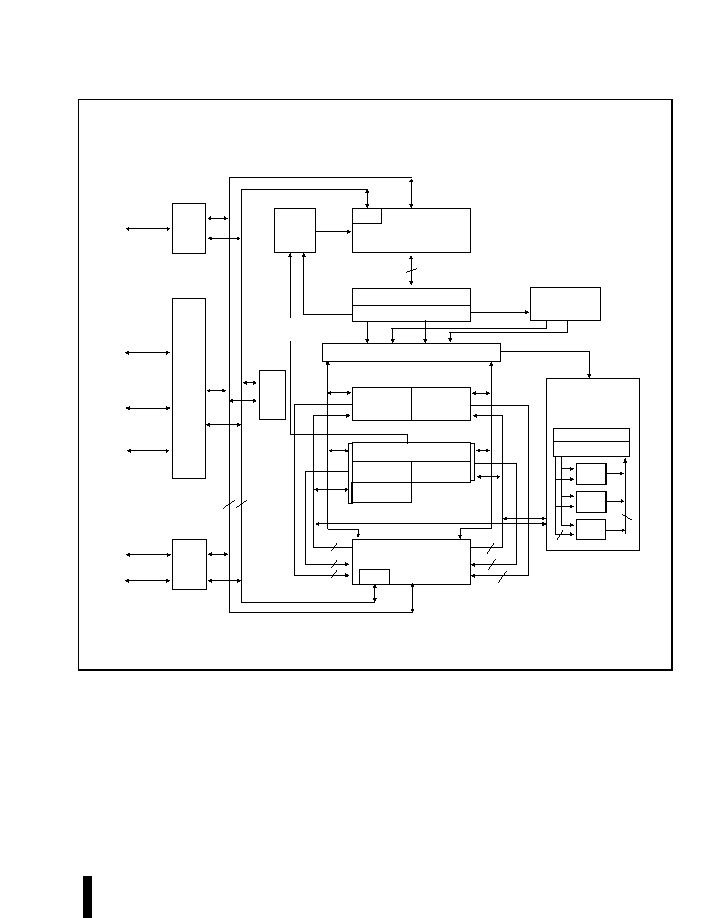
E
PENTIUMģ PROCESSOR 75/90/100/120/133/150/166/200
5
Branch
Target
Buffer
Code Cache
8 KBytes
ROM
Control Unit
Generate
Address
Generate
Data Cache
8 KBytes
256
TLB
TLB
Prefetch
Address
Prefetch Buffers
Instruction Decode
Instruction
Pointer
Integer Register File
ALU
Barrel Shifter
32
32
32
32
32
32
Page
Unit
Bus
Unit
64-Bit
Data
Bus
32-Bit
Address
Bus
Control
64-Bit
Data
Bus
32-Bit
Addr.
Bus
64
Control
Register File
Add
Multiply
Divide
Floating
Point
Unit
Pentiumģ Processor (75/90/100/120/133/150/166/200 MHz)
Control
80
80
Address
(U Pipeline)
(V Pipeline)
(U Pipeline)
(V Pipeline)
ALU
Branch Verification
and Target Address
32
DP
Logic
Control
APIC
Data
Control
199718
Figure 1. Pentium
ģ
Processor Block Diagram
The block diagram shows the two instruction
pipelines, the "u" pipe and the "v" pipe. The u-pipe
can execute all integer and floating point
instructions. The v-pipe can execute simple integer
instructions and the FXCH floating-point
instructions.
The separate code and data caches are shown.
The data cache has two ports, one for each of the
two pipes (the tags are triple ported to allow
simultaneous inquire cycles). The data cache has
a dedicated Translation Lookaside Buffer (TLB) to
translate linear addresses to the physical
addresses used by the data cache.
The code cache, branch target buffer and prefetch
buffers are responsible for getting raw instructions
into the execution units of the Pentium processor.
Instructions are fetched from the code cache or
from the external bus. Branch addresses are
remembered by the branch target buffer. The code
cache TLB translates linear addresses to physical
addresses used by the code cache.