 | –≠–ª–µ–∫—Ç—Ä–æ–Ω–Ω—ã–π –∫–æ–º–ø–æ–Ω–µ–Ω—Ç: STEL-1109 | –°–∫–∞—á–∞—Ç—å:  PDF PDF  ZIP ZIP |
Document Outline
- KEY FEATURES
- INTRODUCTION
- PIN CONFIGURATION
- POWER SUPPLY PINS
- FUNCTIONAL BLOCK DIAGRAM DESCRIPTIONS
- TIMING DIAGRAMS
- BURST TIMING EXAMPLES
- ELECTRICAL SPECIFICATIONS
- RECOMMENDED INTERFACE CIRCUITS
- EXAMPLE OUTPUT LOAD SCHEMATIC
- MECHANICAL SPECIFICATIONS

R
STEL-1109/CR
5 - 65 MHz
Burst Transmitter
STEL-1109
Data Sheet

STEL-1109
2
PRELIMINARY PRODUCT INFORMATION
TABLE OF CONTENTS
TRADEMARKS ................................................................................................................................................................
4
KEY FEATURES................................................................................................................................................................
5
INTRODUCTION ............................................................................................................................................................
6
PIN CONFIGURATION .................................................................................................................................................
7
POWER SUPPLY PINS....................................................................................................................................................
7
FUNCTIONAL BLOCK DIAGRAM DESCRIPTIONS............................................................................................
8
Overview ........................................................................................................................................................................
8
Data Path Description ...................................................................................................................................................
9
Bit Sync Block .............................................................................................................................................................
9
Bit Encoder Block.......................................................................................................................................................
10
Data Path Control (Multiplexers)........................................................................................................................
10
Scrambler ................................................................................................................................................................
11
Reed-Solomon Encoder.........................................................................................................................................
12
Symbol Mapper Block...............................................................................................................................................
13
Bit Mapper..............................................................................................................................................................
13
Differential Encoder ..............................................................................................................................................
14
Symbol Mapper......................................................................................................................................................
15
Nyquist Fir Filter .......................................................................................................................................................
18
Interpolating Filter ....................................................................................................................................................
19
Modulator ...................................................................................................................................................................
20
10-Bit DAC..................................................................................................................................................................
20
Control Unit Description..............................................................................................................................................
20
Bus Interface Unit ......................................................................................................................................................
20
Clock Generator .........................................................................................................................................................
20
NCO.............................................................................................................................................................................
21
TIMING DIAGRAMS.....................................................................................................................................................
23
Clock Timing..................................................................................................................................................................
23
Pulse Width ....................................................................................................................................................................
23
Bit Clock Synchronization............................................................................................................................................
24
Input Data and Clock Timing......................................................................................................................................
25
Write Timing ..................................................................................................................................................................
26
Read Timing ...................................................................................................................................................................
27
NCO Loading (User Controlled) .................................................................................................................................
28
NCO Loading (Automatic) ..........................................................................................................................................
28
Digital Output Timing ..................................................................................................................................................
29
DATAEN to DATAENO Timing ................................................................................................................................
30
BURST TIMING EXAMPLES........................................................................................................................................
30
Burst Timing: Full Burst (Slave Mode, QPSK) ..........................................................................................................
31
Master Mode, BPSK Burst Timing Signal Relationships .........................................................................................
32
Slave Mode, BPSK Burst Timing Signal Relationships ............................................................................................
32
Master Mode, QPSK Burst Timing Signal Relationships ........................................................................................
33
Slave Mode, QPSK Burst Timing Signal Relationships ...........................................................................................
33
Master Mode, 16QAM Burst Timing Signal Relationships ....................................................................................
34
Slave Mode, 16QAM Burst Timing Signal Relationships........................................................................................
34
ELECTRICAL SPECIFICATIONS ................................................................................................................................
35
RECOMMENDED INTERFACE CIRCUITS ..............................................................................................................
38
Slave Mode Interface.....................................................................................................................................................
38
Master Mode Interface..................................................................................................................................................
38
EXAMPLE OUTPUT LOAD SCHEMATIC ................................................................................................................
39
MECHANICAL SPECIFICATIONS .............................................................................................................................
39

PRELIMINARY PRODUCT INFORMATION
3
STEL-1109
LIST OF ILLUSTRATIONS
Figure 1.
STEL-1109 Block Diagram....................................................................................................................
9
Figure 2.
Bit Encoder Functional Diagram ........................................................................................................ 10
Figure 3.
Scrambler Block Diagram .................................................................................................................... 11
Figure 4.
DAVIC Scrambler.................................................................................................................................. 12
Figure 5.
Mapping Block Functional Diagram .................................................................................................. 13
Figure 6.
BPSK Constellation ............................................................................................................................... 15
Figure 7.
QPSK Constellation .............................................................................................................................. 16
Figure 8.
Natural Mapping Constellation.......................................................................................................... 16
Figure 9.
Gray Coded Constellation ................................................................................................................... 17
Figure 10.
Left Coded Constellation ..................................................................................................................... 17
Figure 11.
DAVIC Coded Constellation ............................................................................................................... 18
Figure 12.
Right Coded Constellation .................................................................................................................. 18
Figure 13.
Nyquist FIR Filter.................................................................................................................................. 19
Figure 14.
Interpolation Filter Block Diagram..................................................................................................... 19
Figure 15.
Duty Cycle Derating Versus Temperature (@3.3v).......................................................................... 36
Figure 16.
STEL-1109 Mechanical Characteristics .............................................................................................. 39

STEL-1109
4
PRELIMINARY PRODUCT INFORMATION
LIST OF TABLES
Table 1.
STEL-1109 Features ..............................................................................................................................
5
Table 2.
I/O Signal Pin Assignments................................................................................................................
7
Table 3.
STEL -1109 Configuration Register Data Fields...............................................................................
8
Table 4.
Data Latching Options .........................................................................................................................
9
Table 5.
Bit Encoding Data Path Options......................................................................................................... 11
Table 6.
Scrambler Parameters .......................................................................................................................... 11
Table 7.
Sample Scramble Register Values ...................................................................................................... 12
Table 8.
Reed-Solomon Encoder Parameters................................................................................................... 13
Table 9.
Bit Mapping Options............................................................................................................................ 14
Table 10.
Differential Encoder Control............................................................................................................... 14
Table 11.
Qpsk Differential Encoding and Phase Shift .................................................................................... 15
Table 12.
Symbol Mapping Selections................................................................................................................ 16
Table 13.
Symbol Mapping .................................................................................................................................. 17
Table 14.
FIR Filter Configuration Options ....................................................................................................... 18
Table 15.
FIR Filter Coefficient Storage.............................................................................................................. 18
Table 16.
Interpolation Filter Bypass Control.................................................................................................... 19
Table 17.
Interpolation Filter Signal Level Control .......................................................................................... 19
Table 18.
Signal Inversion Control...................................................................................................................... 20
Table 19.
FCW Selection ....................................................................................................................................... 22
Table 20.
Clock Timing AC Characteristics ....................................................................................................... 23
Table 21.
Pulse Width AC Characteristics ......................................................................................................... 23
Table 22.
Bit Clock Synchronization AC Characteristics ................................................................................. 24
Table 23.
Input Data and Clock AC Characteristics ......................................................................................... 25
Table 24.
Write Timing AC Characteristics ....................................................................................................... 26
Table 25.
Read Timing AC Characteristics ........................................................................................................ 27
Table 26.
NCO Loading AC Characteristics ...................................................................................................... 28
Table 27.
Digital Output Timing AC Characteristics ....................................................................................... 29
Table 28.
DATAEN to DATAENO Timing AC Characteristics...................................................................... 30
Table 29.
Absolute Maximum Ratings ............................................................................................................... 35
Table 30.
Recommended Operating Conditions ............................................................................................... 36
Table 31.
DC Characteristics ................................................................................................................................ 37
TRADEMARKS
Stanford Telecom
Æ
and STEL
Æ
are registered trademarks of Stanford Telecommunications, Incorporated.

PRELIMINARY PRODUCT INFORMATION
5
STEL-1109
KEY FEATURES
n
Complete BPSK/QPSK/16QAM modulator in
a CMOS ASIC
n
Programmable over a wide range of data
rates
n
NCO modulator provides fine frequency
resolution
n
165 MHz maximum clock rate generates a
modulated carrier at frequencies
programmable from 5 to 65 MHz
n
Operates in continuous and burst modes
n
Differential Encoder, Programmable
Scrambler, and Programmable
Reed-Solomon FEC Encoder
n
Programmable 32-tap FIR Filter for signal
shaping before modulation
n
10-bit DAC implemented on chip
n
Complete upstream modulator solution ≠
serial data in and RF signal out
n
Compatible with DAVIC, IEEE 802.14
(preliminary), Intelsat IESS-308, ITU J.83
Annex A, MCNS Standards
n
Supports low data rates for voice
applications and high data rates for
wideband applications
n
Small Footprint, Surface Mount 80-Pin
MQFP Package
Table 1. STEL-1109 Features
Feature
Characteristic
Carrier frequency:
5 to 65 MHz (maximum of approximately 40% of master clock)
Symbol rate:
From Master clock divided by 16 down to Master clock divided by
16384 (in steps of 4) yielding a maximum symbol rate of 10Msps with a
160 MHz clock.
FIR filter tap coefficients:
32 programmable taps (10 bits each), symmetric response
Modulation:
BPSK, QPSK, or 16QAM
16QAM constellation:
Eight selectable bit-to-symbol mappings
Five selectable symbol-to-constellation mappings
I and Q modulator signs / Spectral
Inversion
Signs of I and Q plus the mapping to Sine and Cosine carriers is
programmable.
Reed-Solomon encoder:
Selectable on/off
Two selectable generator polynomials
Block length shortened any amount
Error correction capability T = 1 to 10
Scrambler:
Selectable on/off
Self-synchronizing or frame synchronized (sidestream)
Location before or after RS Encoder
Programmable generator polynomial
Programmable length up to 2
24
- 1
Programmable initial seed
Differential encoder:
Selectable on/off

STEL-1109
6
PRELIMINARY PRODUCT INFORMATION
INTRODUCTION
The STEL-1109
1
is a highly integrated, maximally
flexible, burst transmitter targeted to the cable modem
market. It receives serial data, randomizes the data,
performs FEC and differential encoding, maps the data
to a constellation before modulation, and outputs an
analog RF signal.
The STEL-1109 is the latest in a series of modulator
chips that comprise the STEL-1103 through STEL-1108
modulators. Several key components (e.g., a 10-bit
DAC, FECs, etc.) have been incorporated in the
STEL-1109 and the enhancements have resulted in
significant changes to the chip’s electrical and software
interfaces.
The STEL-1109 is capable of operating at data rates of
up to 10 Mbps in BPSK mode, 20 Mbps in QPSK mode,
and 40 Mbps in 16QAM mode. It operates at clock
frequencies of up to 165 MHz, which allows its internal,
10-bit Digital-to-Analog Converter (DAC) to generate
RF carrier frequencies of 5 to 65 MHz.
The STEL-1109 also uses digital FIR filtering to
optimally shape the spectrum of the modulating data
prior to modulation. This optimizes the spectrum of
the modulated signal, and minimizes the analog
filtering required after the modulator. The filters are
1
The STEL-1109 utilizes advanced signal processing
techniques which are covered by U.S. Patent Number
5,412,352.
designed to have a symmetrical (mirror image)
polynomial transfer function, thereby making the phase
response of the filter linear. This also eliminates the
inter-symbol interference that results from group delay
distortion. In this way, it is possible to change the
carrier frequency over a wide frequency range without
having to change filters, thus providing the ability to
operate a single system in many channels.
The STEL-1109 can operate with very short gaps
between transmitted bursts to increase the efficiency of
TDMA systems. The STEL-1109 (as well as the STEL-
1103 and STEL-1108) operates properly even when the
interburst gap is less than four (4) symbols (half the
length of the FIR filter response). In this case the
postcursor of the previous burst overlaps and is
superimposed on the precursor of the following burst.
Signal level scaling is provided after the FIR filter to
allow the STEL-1109’s maximum arithmetic dynamic
range to be utilized. Signal levels can be changed over
a wide range depending on how the device is
programmed.
In addition, the STEL-1109 is designed to operate from
a 3.3 Vdc power supply and the chip can be interfaced
with logic that operates at 5 Vdc.
PRELIMINARY PRODUCT INFORMATION
7
STEL-1109
PIN CONFIGURATION
The STEL-1109 input and output signal pin
assignments are listed in Table 2. The location of the
pin numbers is shown by Figure 16 (page 39). The
STEL-1109 power supply pins are described in the
following paragraph.
Table 2. I/O Signal Pin Assignments
1
V
DD
[7]
(S)
21 FCWSEL
1
[21]
(I)
41 V
DD
[7]
(S)
61 V
SS
[7]
(T)
2
DATA
4
[20] (B)
22 V
SS
[7]
(T)
42 SYMPLS
[20]
(O)
62 V
DD
[7]
(S)
3
DATA
5
[20] (B)
23 V
SS
[7]
(T)
43 V
SS
[7]
(S)
63 V
DD
[7]
(T)
4
DATA
6
[20] (B)
24 V
SS
[7]
(T)
44 V
SS
[7]
(T)
64 V
SS
[7]
(S)
5
DATA
7
[20] (B)
25 V
DD
[7]
(S)
45 V
SS
[7]
(T)
65 V
DD
[7]
(T)
6
V
SS
[7]
(S)
26 CLKEN
[9,20] (I)
46 V
SS
[7]
(T)
66 V
SS
[7]
(S)
7
V
SS
[7]
(S)
27 V
SS
[7]
(S)
47 V
SS
[7]
(T)
67 RSTB
[20]
(I)
8
ADDR
5
[20]
(I)
28 CLK
[20]
(I)
48 V
SS
[7]
(T)
68 V
SS
[7]
(T)
9
ADDR
4
[20]
(I)
29 RDSLEN
[10]
(I)
49 V
SS
[7]
(S)
69 V
SS
[7]
(S)
10 ADDR
3
[20]
(I)
30 V
DD
[7]
(S)
50
[7] (N.C.)
70 DIFFEN
[13]
(I)
11 V
DD
[7]
(S)
31 5V
DD
[7]
(I)
51 AV
DD
[7]
(S)
71 NCO LD
[21]
(I)
12 ADDR
2
[20]
(I)
32 SCRMEN
[10]
(I)
52 OUT
[20] (AO)
72
CSEL
[20]
(I)
13 ADDR
1
[20]
(I)
33 V
SS
[7]
(S)
53 OUTN
[20] (AO)
73
DSB
[20]
(I)
14 ADDR
0
[20]
(I)
34 V
SS
[7]
(T)
54 AV
SS
[7]
(S)
74
WR
[20]
(I)
15 V
SS
[7]
(S)
35 CKSUM
[12]
(O)
55
[7] (N.C.)
75 V
DD
[7]
(S)
16 V
SS
[7]
(S)
36 V
SS
[7]
(S)
56 V
SS
[7]
(S)
76 DATA
0
[20]
(B)
17 TSDATA
[9]
(I)
37 ACLK
[20]
(O)
57 V
SS
[7]
(T)
77 DATA
1
[20]
(B)
18 DATAEN
[10]
(I)
38 V
DD
[7]
(S)
58 V
SS
[7]
(T)
78 DATA
2
[20]
(B)
19 TCLK
[9]
(I)
39 DATAENO [20]
(O)
59 V
SS
[7]
(T)
79 DATA
3
[20]
(B)
20 FCWSEL
0
[21]
(I)
40 BITCLK
[9,20] (O)
60 V
SS
[7]
(T)
80 V
SS
[7]
(S)
Notes:
1.
Pin 31 is applied to input buffers only.
2.
See Package Outline (Figure 16) for pin
identification.
Legend:
(AO)
Analog Output
(O)
Output signal
(B)
Bi-directional (I/O) signal
(S)
Source
(I)
Input signal
(T)
Factory Test Pin
(N.C.)
Not Connected
[#]
Page Reference
POWER SUPPLY PINS
There are three separate power supply systems within
the STEL-1109. The primary supply for the digital logic
circuits is nominally 3.3 volts and is input on the V
DD
pins. The digital inputs have a separate supply, 5V
DD
,
which can be connected to a 5 volt supply if the STEL-
1109 inputs are driven from 5 volt logic. If the logic
driving the STEL-1109 is run on 3.3 volts, then the 5V
DD
pin should be connected to 3.3 volts. The return for
both digital supplies is V
SS
. The DAC has a separate
analog power supply and return, AV
DD
and AV
SS
. The
3.3 volt AV
DD
input allows the user to provide a
separate well filtered supply for the DAC to prevent
spurs that might be created from digital noise on the
V
DD
supply system.

STEL-1109
8
PRELIMINARY PRODUCT INFORMATION
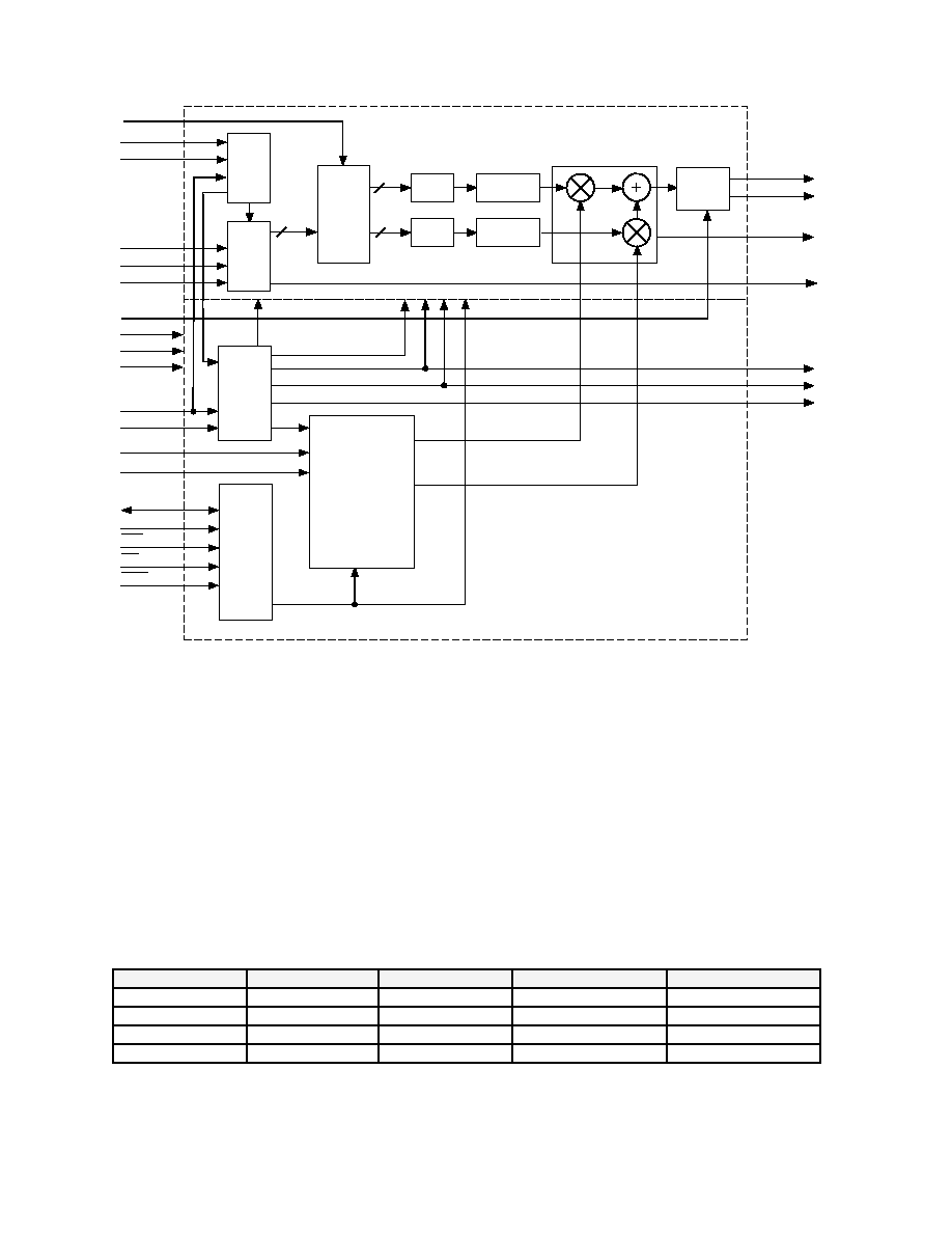
FUNCTIONAL BLOCK DIAGRAM DESCRIPTIONS
OVERVIEW
The STEL-1109 is comprised of the Data Path and
Control Unit sections shown in Figure 1. The Data Path
is comprised of a Bit Sync Block, Bit Encoder Block
(i.e., the Scrambler, Reed-Solomon Encoder, and two
Multiplexers shown in Figure 2), Symbol Mapper Block
(i.e., the Bit Mapper, Differential Encoder, and Symbol
Mapper are shown in Figure 5), two channels (one for I
and one for Q), a Combiner, and a 10-bit DAC. Each
channel consists of a Nyquist Filter, Interpolation Filter,
and Modulator. The Control Unit is comprised of a Bus
Interface Unit (BIU), Clock Generator, and NCO.
Table 1 summarizes the main features of the circuits
described by the remaining paragraphs of this section.
The STEL-1109 provides 58, programmable, read/write
registers (Configuration Registers). Table 3 provides a
graphic representation of the STEL-1109’s
Configuration Registers and their data fields. Each
register can be selected for a write or read operation
using addresses 00
H
through 39
H
.
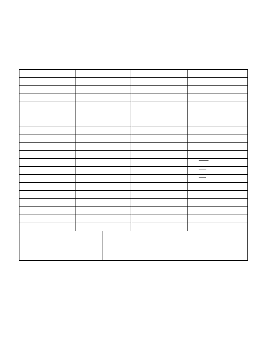
Table 3. STEL-1109 Configuration Register Data Fields
Address
Contents
(Hex)
Bit 7
Bit 6
Bit 5
Bit 4
Bit 3
Bit 2
Bit 1
Bit 0
08 - 00
NCO
21
28 - 09
FIR Filter Coefficients
18
29
LSB Sampling Rate Control (see address 39 for MSB)
20
2A
Interpolation Filter Gain Control
19
Auxiliary Clock Rate Divider
20
2B
Set To Zero
Set To Zero
Interpolation Filt. Bypass
19
Set To One
Set To Zero
Invert I/Q Chan.
20
2C
TCLK Sel.
9
Set To Zero
Set To Zero
Set To Zero
MOD
14
FIR bypass
18
Set To Zero
2D
FZSINB
21
Bit Mapping
13
Set To One
Set To Zero
PN Code Sel
9
PN On/Off
9
2E
Symbol Mapping
15
CLRFIR
18
Bit Sync Re-arm
9
2F
Set To Zero
32-30
SCRAMBLER Init Registers
11
35-33
SCRAMBLER Mask Registers
11
36
PPolynomial
13
BypassB
10
S-RS
10
Self-Sync
11
T
12
37
K
12
38
DATAENBPB
10
DATAENSEL
10
RSENBPB
10
RSENSEL
10
SCRMENBPB
10
SCRMENSEL
10
DiffDCBPB
14
DiffDCSEL
14
39
Set To Zero
Set To Zero
TRLSBF
12
LDLSBF
12
MSB Sampling Rate Control (see address 29 for LSB)
20
Note:
Superscripted numbers are page references where discussion on setting the particular register(s)
or bit(s) begins.
PRELIMINARY PRODUCT INFORMATION
9
STEL-1109
OUT
10-Bit
DAC
OUTN
Modulator
DATAENO
CKSUM
BITCLK
SYMPLS
ACLK
WCP 52981.c-5/2/97
CONTROL UNIT
SIN 2
FT
COS 2
FT
Numerically
Controlled
Oscillator
Bus
Interface
Unit
CSEL
WR
DSB
ADDR
5-0
DATA
7-0
FCWSEL
1-0
NCO LD
CLK
CLKEN
RST
VDD
5VDD
AVDD
SCRMEN
RDSLEN
DATAEN
TSDATA
TCLK
DIFFEN
BIT
Sync
Block
BIT
Encoder
Block
Clock
Generator
MASTER CLOCK
SAMPLS
4
2
I[1:0],
Q[1:0]
I[1:0]
2
Q[1:0]
Symbol
Mapper
Block
Nyquist
Filter
Nyquist
Filter
Interpolating
Filter
Interpolating
Filter
DATA PATH
Figure 1. STEL-1109 Block Diagram
DATA PATH DESCRIPTION
BIT SYNC BLOCK
The Bit Sync Block has two functions, latching input
data, and synchronizing the STEL-1109 BITCLK and
symbol counters to the user data.
Latching Input Data
Latching of input data is accomplished in three ways:
∑
Externally supplied TSDATA is latched by the
internal BITCLK.
∑
Externally supplied TSDATA is latched by an
externally provided TCLK
∑
Internally generated PN code data is latched by the
internal BITCLK
See Table 4 for register settings to implement each
mode.
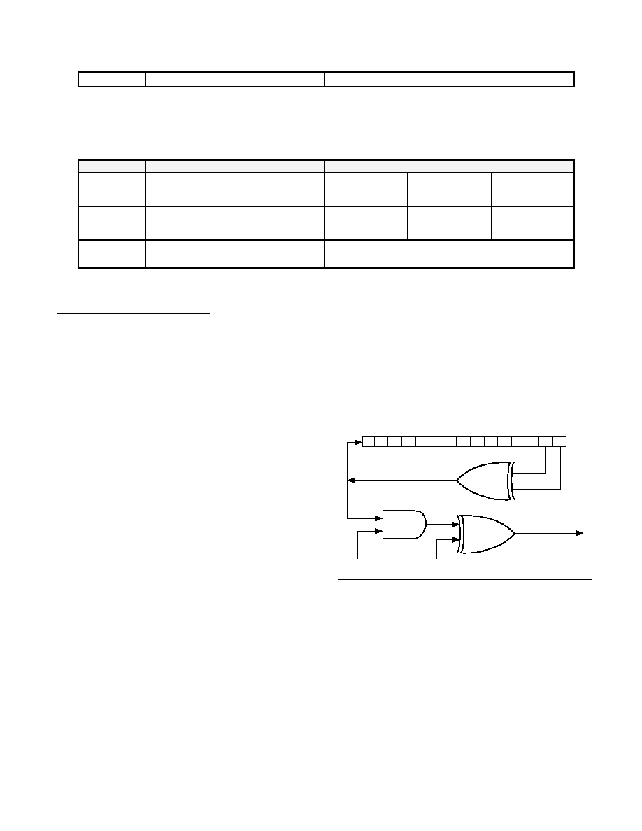
Table 4. Data Latching Options
Data Source
Latched By
Register 2C Bit 7
Register 2D Bits 1,0
Mode Name
TSDATA
BITCLK
0
X,0
Master Mode
TSDATA
TCLK
1
X,0
Slave Mode
PN Code 10, 3
BITCLK
0
0,1
Test Mode
PN Code 23, 18
BITCLK
0
1,1
Test Mode

STEL-1109
10
PRELIMINARY PRODUCT INFORMATION
BITCLK latches data on its falling edge. TCLK latches
data on its rising edge.
Whenever the CLKEN input is low, the BITCLK output
will stop. In order to provide customers with a
continuous clock, the STEL-1109 provides an auxiliary
clock (ACLK) output which is discussed later in the
clock generator section. The ACLK output is primarily
for use in master mode where users may need a clock to
run control circuits during the guard time between
bursts.
When using slave mode, the data that is latched by the
rising edge of TCLK is re-latched internally by the next
falling edge of BITCLK which re-synchronizes the data
to the internal master clock.
Synchronizing BITCLK / SYMPLS
The synchronization circuit aligns the STEL-1109
BITCLK and its SYMPLS counter circuits to the
beginning of the first user data symbol. The circuit has
two parts, an arming circuit and a trigger circuit. Once
armed, the first rising edge on the TCLK input will
activate (trigger) the synchronization process.
The circuit can be armed in two ways; taking CLKEN
from low to high, or toggling Configuration Register
2E
H
bit 0 from low to high to low again. In a normal
burst mode application, the circuit is automatically re-
armed between bursts because CLKEN goes low. For
applications that will not allow CLKEN to cycle low
between bursts, some system level precautions should
be observed to maintain synchronization of user data to
the STEL-1109 BITCLK.
Once triggered, the sync circuit re-starts the BITCLK
and SYMPLS counters. The BITCLK output starts high,
and SYMPLS resets to the start of a symbol. There is a
delay equal to about three cycles of the master clock
from the rising edge of the TCLK input before this re-
start occurs. During this brief delay period, the BITCLK
and SYMPLS counters are still free running and may or
may not have transitions.
In master mode, the rising edge of TCLK normally
marks the transition of the first user data bit (which will
be latched in by the next falling edge of BITCLK). In
slave mode, the first user data bit must already be valid
at this first rising edge of TCLK.
BIT ENCODER BLOCK
The Bit Encoder Block consists of a Scrambler, a
Reed-Solomon Encoder, and data path controls
(multiplexers), as shown in Figure 2.
SERIAL
DATA
DATAEN
ENCODED
SERIAL DATA
Reed-Solomon
Encoder
Scrambler
WCP 52982.c-4/26/97
SCRMEN
S-RS
RDSLEN
CHKSUM
SIGNAL
Input
Multiplexer
Output
Multiplexer
Figure 2. Bit Encoder Functional Diagram
Data Path Control (Multiplexers)
The STEL-1109 provides a great deal of flexibility and
control over the routing of data through or around the
encoding functions. With appropriate register
selections, data can be routed around (bypass) both
encoders, through either one and around the other,
through the scrambler then the RS Encoder, or through
the RS Encoder and then the scrambler. Control over
the bypassing can be set for software control or external
(user) input signal control. Generally, if an encoding
function will be left either on or off continuously, then
software control is appropriate. If the function must be
turned on and off dynamically (typically in order to
send the preamble ‘in the clear’ i.e. unencoded), then
external (user) input control is required. If the Reed-
Solomon encoder will not be used at all, then a separate
bypass option can be activated to remove an 8 bit delay
register from the data path that is required if the
possibility of turning on the encoder exists. Each of the
external (user) input control pins (if enabled) turns on
the encoding function when high and bypasses the
function when low.
The DATAEN input signal determines whether or not
data will advance (shift through) the encoding blocks.
The presence of a high on the DATAEN input when the
BITCLK output goes low allows the circuits to advance
data through them. The DATAEN signal is delayed

PRELIMINARY PRODUCT INFORMATION
11
STEL-1109
internally to allow the rising edge of DATAEN to
coincide with the first rising edge of TCLK.
See Table 5 for a summary of register settings required
to achieve the various data path possibilities.
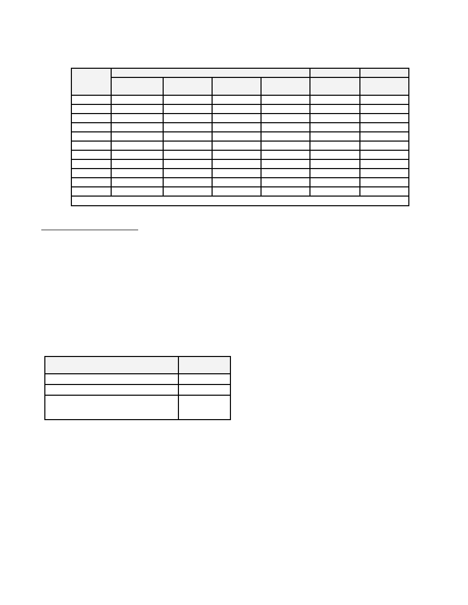
Table 5. BIT Encoding Data Path Options
Data Path
Register 36 Bits 6,5
Register 38 Bits 7-2
Data stopped (continuously)
X,X
01 XX XX
Data path on (continuously)
X,X
11 XX XX
Data path enabled by pin 18
X,X
X0 XX XX
Scrambler off (continuously)
X,X
XX XX 01
Scrambler on (continuously)
X,X
XX XX 11
Scrambler enabled by pin 32
X,X
XX XX X0
RS Encode off (continuously)
1,X
XX 01 XX
RS Encode on (continuously)
1,X
XX 11 XX
RS Encode enabled by pin 29
1,X
XX X0 XX
Scrambler then RS Encoder
1,1
XX XX XX
RS Encoder then Scrambler
1,0
XX XX XX
Bypass RS Encoder
0,X
XX XX XX
Scrambler
The scrambler can be used to randomize the serial data
in order to avoid a strong spectral component that
might otherwise arise from the occurrence of repeating
patterns in the input data. The Scrambler (Figure 3)
uses a Pseudo-Random (PN) generator to generate a PN
code pattern. All 24 registers are presettable and any
combination of the registers can be connected (tapped)
to form any polynomial of up to 24 bits. The scrambler
may be either frame synchronized or self synchronized.
Table 6 shows the registers involved.
The value in the INIT registers is loaded into the
scrambler shift registers whenever the scrambler is
disabled. The scrambler will scramble data one bit at a
time at each falling edge of BITCLK that occurs while
both the scrambler and DATAEN are active (enabled).
Internal delays on the SCRMEN control signal input
allow for a rising edge to occur coincident with the
rising edge of BITCLK that precedes the latching of the
first data bit to be scrambled.
1
2
3
22
23
24
24-bit INIT Reg
1
2
3
22
23
24
24-bit Shift Reg
1
2
3
22
23
24
24-bit Mask Reg
XOR
AND
XOR
SCRMEN
SERIAL INPUT
SSYNC
SERIAL OUTPUT
SELF
SYNC
FRAME
SYNC
MUX
WCP 52983.c-4/26/97
Figure 3. Scrambler Block Diagram
Table 6. Scrambler Parameters
Parameter
Characteristic
Configuration Register Setting
Generator
Polynomial
(Mask Reg)
p(x) = c
24
x
24
+ c
23
x
23
+ … + c
1
x
+ 1
where c
i
is a binary value (0, 1)
Register 35
Bit 7
to
Bit 0
c
24
to
c
17
Register 34
Bit 7
to
Bit 0
c
16
to
c
9
Register 33
Bit 7
to
Bit 0
c
8
to
c
1
Seed
(INIT Reg)
Any 24 bit binary value, s
24-1
Register 32
Bit 7
to
Bit 0
s
24
to
s
17
Register 31
Bit 7
to
Bit 0
s
16
to
s
9
Register 30
Bit 7
to
Bit 0
s
8
to
s
1
Scrambler
Type
Frame synchronized (sidestream)
Register 36 Bit 4
Set to zero
Scrambler
Self-synchronized
Register 36 Bit 4
STEL-1109
12
PRELIMINARY PRODUCT INFORMATION
Type
Set to one
The Mask, Init, and SSync fields can be programmed
for different scrambler configurations. For example, the
DAVIC Scrambler configuration shown in Figure 4 can
be implemented by programming the Mask, Init, and
SSync fields with the values indicated by Table 7.
Table 7. Sample Scramble Register Values
Parameter
Characteristic
Configuration Register Setting
Generator
Polynomial
(Mask Reg)
p(x) = x
15
+ x
14
+ 1
Register 35
Bit 7 to Bit 0
0000 0000
Register 34
Bit 7 to Bit 0
0110 0000
Register 33
Bit 7 to Bit 0
0000 0000
Seed
(INIT Reg)
0000A9 Hex
Register 32
Bit 7 to Bit 0
0000 0000
Register 31
Bit 7 to Bit 0
0000 0000
Register 30
Bit 7 to Bit 0
1010 1001
Scrambler
Type
Frame synchronized (sidestream)
Register 36 Bit 4
Set to zero
Reed
-
Solomon Encoder
The STEL-1109 uses a standard Reed-Solomon (RS)
Encoder for error correction encoding of the serial data
stream.
When DATAEN is high and the RS Encoder is enabled,
the serial data stream both passes straight through the
RS Encoder and also into encoding circuitry. The
encoding circuitry computes a checksum that is 2T
bytes long for every k bytes of input data. After the
last bit of each block of k bytes of input data, the RS
Encoder inserts its checksum (2T bytes of data) into the
data path. There is no adverse effect to letting TCLK or
TSDATA continue to run during the checksum; the data
input will be ignored. CKSUM (pin 35) will be asserted
high to indicate that the checksum bytes are being
inserted into the data stream and will be lowered at the
end of the checksum data insertion. The width of the
CKSUM pulse is 2T bytes.
The STEL-1109 registers include two bits for
determining the bit order for data into and checksum out
of the RS Encoder circuitry. Set these to match the
Reed-Solomon decoding circuitry along with the other
parameters.
The error correction encoding uses GF (256) and can be
programmed for an error correction capability of 1 to
10, a block length of 3 to 255, and one of two primitive
polynomials using the data fields listed in Table 8.
1
2
3
4
5
6
7
8
9
10
11
12
13
14
15
1
0
0
1
0
1
0
1
0
0
0
0
0
0
0
EX-OR
EX-OR
AND
Enable
Clear Data Input
Randomized Data
WCP 52984.c-4/26/97
Figure 4. DAVIC Scrambler

PRELIMINARY PRODUCT INFORMATION
13
STEL-1109
Table 8. Reed-Solomon Encoder Parameters
Field Name
Configuration Register
Description
PP
36
H
(bit 7)
1-bit field for selecting Primitive Polynomial:
0
p(x) = x
8
+ x
4
+ x
3
+ x
2
+ 1
1
p(x) = x
8
+ x
7
+ x
2
+ x + 1
T
36
H
(bits 3-0)
4-bit field for setting Error Correction Capability. Programmable over the range
of 1 to 10.
K
37
H
(bits 7-0)
8-bit field for setting User Data Packet Length (K) in bytes.
Programmable over the range of 1 to (255 - 2T). [ Net block length, N = K + 2T ]
LDLSBF
39
H
(bit 4)
Determines whether the first bit of the serial input is to be the MSB (bit 4 = 0) or
LSB (bit 4 = 1) of the byte applied to the RS Encoder.
TRLSBF
39
H
(bit 5)
Determines whether the MSB (bit 5 = 0) or LSB (bit 5 = 1) of the RS Encoder
checksum byte is to be the first bit of the serial output data.
Notes:
1.
GF (256).
2.
Code generator polynomial 1 is used when PP=0:
G x
x
i
i
T
( )
(
)
=
-
=
=
+
02
H
120
119 2
3.
Code generator polynomial 2 is used when PP=1.
G x
x
i
i
T
( )
(
)
=
-
=
-
0
2
1
= 02
H
SYMBOL MAPPER BLOCK
The Symbol Mapper Block (Figure 5) maps the serial
data bits output by the Bit Encoder Block to symbols,
differentially encodes the symbols, and (in 16QAM)
maps the symbols to one of five constellations. The
Symbol Mapper Block functions are modulation
dependent. The modulation mode also defines the
number of bits per symbol. The Symbol Mapper Block
outputs 2 bits for each symbol to each of the two
Nyquist (FIR) Filters.
ENCODED
SERIAL DATA
I[1:0]
**
Q[1:0]
**
I[1:0]
*
Q[1:0]
*
I[1:0]
Q[1:0]
4
Bit
Mapper
Differential
Encoder
4
2
Symbol
Mapper
2
1
DIFFEN
1
WCP 52985.c-4/26/97
Figure 5. Mapping Block Functional Diagram
Bit Mapper
The Bit Mapper receives serial data and maps the serial
data bits to output symbol bits (I
1
**
, I
0
**
, Q
1
**
, and Q
0
**
).
There are four output bits per symbol even in BPSK and
QPSK modes. In BPSK, all bits are set equal to each
other. In QPSK, each input symbol bit drives a pair of
output bits. The four symbol bits are routed to the
Differential Encoder in parallel.
For BPSK modulation, each bit (symbol = b
0
) of the
input serial data stream is mapped directly to I
1
**
, Q
1
**
,
I
0
**
, and Q
0
**
(i.e., I
1
**
= I
0
**
= Q
1
**
= Q
0
**
= b
0
). Thus, bit
mapping has no affect on the respective value of the
symbol’s four bits, as shown in Table 9.
For QPSK modulation, each pair of bits (a dibit) forms a
symbol (b
0
b
1 )
. The QPSK dibit is mapped so that
I
1
*
= I
0
**
and Q
1
**
=
Q
0
**,
as shown in Table 9.
For 16QAM, every four bits (a nibble) forms a symbol
(b
0
b
1
b
2
b
3
). The 16QAM nibble is mapped to I
1
**
, Q
1
**
, I
0
**
,
and Q
0
**
, as shown in Table 9.
STEL-1109
14
PRELIMINARY PRODUCT INFORMATION
Table 9. Bit Mapping Options
Bit-To-Symbol Mapping
Bit Mapping
Mod Mode
Mode
b
0
b
1
b
2
b
3
Register 2D
bits 6-4
Register 2C bits
3,2
BPSK
I
1
**
Q
1
**
I
0
**
Q
0
**
N/A
N/A
N/A
XXX
1X
QPSK
I
1
**
I
0
**
Q
1
**
Q
0
**
N/A
N/A
XX0
00
QPSK
Q
1
**
Q
0
**
I
1
**
I
0
**
N/A
N/A
XX1
00
16QAM
I
1
**
I
0
**
Q
1
**
Q
0
**
000
01
16QAM
Q
1
**
Q
0
**
I
1
**
I
0
**
001
01
16QAM
I
0
**
I
1
**
Q
0
**
Q
1
**
010
01
16QAM
Q
0
**
Q
1
**
I
0
**
I
1
**
011
01
16QAM
I
1
**
Q
1
**
I
0
**
Q
0
**
100
01
16QAM
Q
1
**
I
1
**
Q
0
**
I
0
**
101
01
16QAM
I
0
**
Q
0
**
I
1
**
Q
1
**
110
01
16QAM
Q
0
**
I
0
**
Q
1
**
I
1
**
111
01
Note: b
0
is the first serial data bit to arrive at the Bit Mapper
Differential Encoder
The Differential Encoder encodes the bits (i.e., I
1
**
, I
0
**
,
Q
1
**
, and Q
0
**
) of each symbol received from the Bit
Mapper to determine the output bit values (i.e., I
1
*
, Q
1
*
,
I
0
*
, and Q
0
*
), which are routed to the Symbol Mapper.
The differential encoder can be either enabled or
bypassed under the control of either a register bit or a
user supplied control signal (DIFFEN pin 70). The
selection between user input pin control or register
control is made in another register bit, as shown in
Table 10.
Table 10. Differential Encoder Control
Level/Value
Register 38
Bits 1,0
Encoding off (continuously)
0,1
Encoding on (continuously)
1,1
Encoding enabled by pin 70
high - enable the Differential Encoder
low - disable the Differential Encoder
X,0
For any modulation mode, if differential encoding is
disabled then:
I
1
*
Q
1
*
I
0
*
Q
0
*
=
I
1
**
I
0
**
Q
1
**
Q
0
**
If differential encoding is enabled, then the results are
described below for each modulation type.
BPSK
In BPSK mode, the next output bit is found by XORing
the input bit with the current output bit. The result is a
180 degree phase change if the output is high and
0 degrees if the output is low.
QPSK
In QPSK mode, the next output dibit is found by
XORing the input dibit with the current output dibit.
Table 11 shows the results of the differential encoding
performed for QPSK modulation and the resulting
phase shift. In the table, I = I
1
= I
0
and Q = Q
1
= Q
0
.
16QAM
In 16QAM mode, the differential encoding algorithm is
the same as in QPSK. Only the two MSB’s, I
1
**
and Q
1
**
are encoded. The output bits I
0
*
and Q
0
*
are set equal to
the inputs bits I
0
**
and Q
0
**
.
PRELIMINARY PRODUCT INFORMATION
15
STEL-1109
Table 11. QPSK Differential Encoding and Phase Shift
Current Input
(IQ)
Current Output
(IQ)
Next Output
(IQ)
Phase Shift
(degrees)
00
00
00
0
01
01
-90 (CW)
10
10
90 (CCW)
11
11
180
01
00
01
-90 (CW)
01
11
180
10
00
0
11
10
90 (CCW)
10
00
10
90 (CCW)
01
00
0
10
11
180
11
01
90 (CCW)
11
00
11
180
01
10
90 (CCW)
10
01
-90 (CW)
11
00
0
Symbol Mapper
The Symbol Mapper receives I
1
*
, Q
1
*
, I
0
*
, Q
0
*
of each
symbol. Based on the signal modulation and the
symbol mapping selection, the Symbol Mapper block
maps the symbol to a constellation data point
(I
1
,Q
1
,I
0
,Q
0
). The Symbol Mapping field (bits 7-5 of
Configuration Register 2E
H
) will map the four input bits
to a new value, as indicated in Table 12.
For BPSK and QPSK, the settings of the symbol to
constellation mapping bits is ignored. The
constellations for BPSK (Figure 6) and QPSK (Figure 7)
are shown below. I
1
Q
1
values are indicated by large,
bold font (
00
and
11)
and I
0
Q
0
values by the smaller
font (00 and 11).
00
11
00
11
1
3
-1
-3
-3
-1
1
3
Q
I
WCP 52999.c-10/29/97
Figure 6. BPSK Constellation
STEL-1109
16
PRELIMINARY PRODUCT INFORMATION
1
3
-1
-3
-3
-1
1
3
00
10
01
11
Q
I
00
10
11
01
WCP 52986.c-10/29/97
Figure 7. QPSK Constellation
16QAM
For 16QAM modulation, the Symbol Mapper maps
each input symbol to one of the 16QAM constellations.
The specific constellation is programmed by the Symbol
Mapping field (bits 7-5 of Configuration Register 2E
H
)
to select the type of symbol mapping. If the MSB of the
Symbol Mapping field is set to 0, the mapping will be
bypassed and I
1
Q
1
I
0
Q
0
= I
1
*
Q
1
*
I
0
*
Q
0
*
. The resulting
constellation (Figure 8) is the natural constellation for
the STEL-1109.
If the MSB of the Symbol Mapping field is set to 1, bits
6-5 can select any of four possible types of symbol
mapping (Gray, DAVIC, Left, or Right), as indicated by
Table 12.
Table 13 summarizes the symbol mapping and the
resulting constellations are shown in Figure 8 and
Figure 9. In these figures, I
1
Q
1
are indicated by large,
bold font (
00, 01, 10,
and
11)
and I
0
Q
0
by the
smaller font (00, 01, 10, and 11).
11
00
11
01
1
-3
-1
1
3
Q
I
01
10
11
00
10
11
10
01
00
10
00
11
01
00
01
WCP 52987.c-10/29/97
10
Figure 8. Natural Mapping Constellation
Table 12. Symbol Mapping Selections
Mapping
Selection
Register 2E
Bits 7-5
Natural
0XX
Gray
100
DAVIC
101
Left
110
Right
111
PRELIMINARY PRODUCT INFORMATION
17
STEL-1109
Table 13. Symbol Mapping
Input Code
Natural
Mapping
(Bypass)
Gray
DAVIC
Left
Right
Output
Code
I
1
*
Q
1
*
I
0
*
Q
0
*
I
1
*
Q
1
*
I
0
*
Q
0
*
I
1
*
Q
1
*
I
0
*
Q
0
*
I
1
*
Q
1
*
I
0
*
Q
0
*
I
1
*
Q
1
*
I
0
*
Q
0
*
I
1
Q
1
I
0
Q
0
0000
0011
0011
0011
0011
0000
0001
0010
0001
0010
0001
0001
0010
0001
0010
0001
0010
0010
0011
0000
0000
0000
0000
0011
0100
0110
0110
0101
1010
0100
0101
0111
0111
0111
1011
0101
0110
0100
0100
0100
1000
0110
0111
0101
0101
0110
1001
0111
1000
1001
1001
1010
0101
1000
1001
1000
1000
1000
0100
1001
1010
1011
1011
1011
0111
1010
1011
1010
1010
1001
0110
1011
1100
1100
1100
1100
1100
1100
1101
1101
1110
1101
1110
1101
1110
1110
1101
1110
1101
1110
1111
1111
1111
1111
1111
1111
00
11
11
01
1
-3
-1
1
3
Q
I
10
01
11
00
10
11
01
10
00
10
00
11
01
00
10
01
WCP 52988.c-10/29/97
Figure 9. Gray Coded Constellation
11
00
11
10
1
-3
-1
1
3
Q
I
01
10
11
00
01
11
01
10
00
01
00
11
10
00
10
01
WCP 52989.c-4/26/97
Figure 10. Left Coded Constellation
STEL-1109
18
PRELIMINARY PRODUCT INFORMATION
11
00
11
01
1
-3
-1
1
3
Q
I
10
10
11
00
10
11
10
01
00
10
00
11
01
00
01
10
WCP 52990.c-4/26/97
Figure 11. DAVIC Coded Constellation
11
00
11
01
1
-3
-1
1
3
Q
I
10
01
11
00
10
11
10
01
00
10
00
11
01
00
01
10
WCP 52991.c-4/26/97
Figure 12. Right Coded Constellation
NYQUIST FIR FILTER
The finite impulse response (FIR) filters are used to
shape each transmitted symbol pulse by filtering the
pulse to minimize the sidelobes of its spectrum. The
Symbol Mapper Block outputs the I
1
I
0
data to a pair of
I-channel FIR filters and the Q
1
Q
0
data to a pair of
Q-channel FIR filters. Figure 13 shows the filter block
diagram for a channel pair (I or Q). The FIR filter can
be bypassed altogether or, in BPSK or QPSK modes,
individual channels can be turned on and off which
changes the effective filter gain. Table 14 shows the
various FIR configuration options.
Table 14. FIR Filter Configuration Options
Mode
Gain
Register 2E
Bits 4-1
Register 2C
Bit 1
No FIR Filter
N/A
XXXX
1
16QAM
Unity
1010
0
BPSK/QPSK
Unity
0000
0
BPSK/QPSK
x2
1111
0
BPSK/QPSK
x3
1010
0
Each of the 32 -tap, linear phase, FIR filters use
16 ten-bit, coefficients, which are completely pro-
grammable for any symmetrical (mirror image) poly-
nomial. The FIR filter coefficients are stored in
addresses 09
H
- 28
H
, using two addresses for each 10-bit
coefficient as shown in Table. The coefficients are stored
as Two’s Complement numbers in the range -512 to
+511 (200
H
to 1FF
H
). The filter is always constrained to
have symmetrical coefficients, resulting in a linear
phase response. This allows each coefficient to be
stored once for two taps, as shown in Table 15.
Table 15. FIR Filter Coefficient Storage
MSB
(Bits 9-8)
LSB
(Bits 7-0)
Filter Taps
0A
H
09
H
Taps 0 and 31
0C
H
0B
H
Taps 1 and 30
0E
H
0D
H
Taps 2 and 29
10
H
0F
H
Taps 3 and 28
…
…
…
…
…
…
22
H
21
H
Taps 12 and 19
24
H
23
H
Taps 13 and 18
26
H
25
H
Taps 14 and 17
28
H
27
H
Taps 15 and 16
Note:
For MSB storage, only bits 1-0 are used.

PRELIMINARY PRODUCT INFORMATION
19
STEL-1109
CLRFIR
BYPASS
2
WCP-52992.c-4/26/97
I
1
/Q
1
COEFFICIENT
I
0
/Q
0
OUT
L
O
G
I
C
M
U
X
M
U
X
1
1
0
0
FIR
FIR
X2
Figure 13. Nyquist FIR Filter
INTERPOLATING FILTER
The Interpolating Filter, shown in Figure 14, is a
configurable, three-stage, interpolating filter. The filter
increases the STEL-1109’s sampling rate (to permit the
wide range of RF carrier frequencies possible) by
interpolating between the FIR filter steps at the master
clock frequency. This smoothes the digital
representation of the signal which removes spurious
signals from the spectrum.
WCP 52993.c-5/2/97
3-Stage
Integrator
11
32
G
a
i
n
16
Gain Control
Master Clock
4
3-Stage
Differentiator
16
Sample
Clock
2
Bypass
Data Enable
Figure 14. Interpolation Filter Block Diagram
The interpolation filter contains accumulators. As the
interpolation ratio grows larger, the number of
accumulations per period of time increases. If the
interpolation ratio becomes too large, the accumulator
will overflow which will destroy the output spectral
characteristics. To compensate for this, the
interpolation filter has a gain function. This gain is
normally set empirically. If the output spectrum is
broad band noise or if it appears correct but has regular
momentary “hits” of broad band spectral noise, then
the digital gain is too high. The interpolation filter gain
is the first place to adjust gain because it does not
directly affect the shape of the signal spectrum and it
has a very wide adjustment range. Overall, gain can
affected in the FIR filter function, the interpolation gain
function, and by the number of interpolation stages
(and therefore accumulators) used.
Normally, three interpolation stages are used, but there
is a bypass option for use when the interpolation is very
high. It should be used only as a last resort after all
other gain reduction options have been exercised
because of the severe impact to spurious performance.
The register bits that affect the interpolation filter
functions are shown inTable 16 and Table 17.
Table 16. Interpolation Filter Bypass Control
Number of
Interpolation Stages
Selected
Interpolation Filter Bypass
Register 2B Bits 5,4
3
0 0
2
0 1
2
1 0
1
1 1
Table 17. Interpolation Filter Signal Level Control
Gain Factor
(Relative)
Filter Gain Control
Register 2A Bits 7-4
2
0
0
H
2
1
1
H
2
2
2
H
2
3
3
H
2
4
4
H
2
5
5
H
2
6
6
H
2
7
7
H
2
8
8
H
2
9
9
H
2
10
A
H
2
11
B
H
2
12
C
H
2
13
D
H
2
14
E
H
2
15
F
H
STEL-1109
20
PRELIMINARY PRODUCT INFORMATION
MODULATOR
The interpolated I and Q data signals are input from the
Interpolation Filter, fed into two complex modulators,
and multiplied by the sine and cosine carriers which are
generated by the NCO. The I channel signal is
multiplied by the cosine output from the NCO and the
Q channel signal is multiplied by the sine output. The
resulting modulated sine and cosine carriers are
applied to an adder and either added or subtracted
together according to the register settings shown in
Table 18. This provides control over the characteristics
of the resulting RF signal by allowing either or both of
the two products to be inverted prior to the addition.
Data Enable Output. The DATAENO output pin is a
modified replica of the DATAEN input. DATAENO is
asserted as a high 2 symbols after DATAEN goes high
and it is asserted as a low 13 symbols after DATAEN
goes low. In this way, a high on the DATAENO line
indicates the active period of the DAC during
transmission of the data burst. However, if the guard
time between the current and next data burst is less
than 13 symbols, then the DATAENO line will be held
high through the next burst.
Table 18. Signal Inversion Control
Output of Adder Block
Invert I/Q Channel
Register 2B Bits 1,0
Sum = I . cos(
t) + Q . sin(
t)
0 0
Sum = –I . cos(
t) + Q . sin(
t)
0 1
Sum = I . cos(
t) – Q . sin(
t)
1 0
Sum = –I . cos(
t) – Q . sin(
t)
1 1
10-BIT DAC
The 10-bit Digital-to-Analog Converter (DAC) receives
the modulated digital data and the Master clock. The
DAC samples the digital data at the rate of the Master
clock and outputs a direct analog RF signal at a
frequency of 5 to 65 MHz. The DAC outputs, OUT and
OUTN, are complementary current sources designed to
drive double terminated 50
or 75
(25
or 37.5
total) load to ground. The nature of digitally sampled
signals creates an image spur at a frequency equal to
the Master Clock minus the output RF frequency. This
image spur should be filtered by a user supplied low
pass filter. For best overall spurious performance, the
gain of the STEL-1109 should be the highest possible
(before digital overflow occurs - see Interpolation Filter
discussion).
CONTROL UNIT DESCRIPTION
BUS INTERFACE UNIT
The Bus Interface Unit (BIU) contains the Configuration
Registers (58 programmable 8-bit registers). The Reset
(
RST
) input signal is the master reset for the
STEL-1109. Asserting a low on
RST
will reset the
contents of all Configuration Registers to 00
H
(as well as
clearing the data path registers). Asserting a high on
RST
enables normal operation. After power is applied
and prior to configuring the STEL-1109, a low should
be asserted on
RST
. Since
RST
is asynchronous, the
CLKEN input should be held low whenever
RST
is
low.
The parallel address bus (ADDR
5-0
) is used to select
one of the 58 Configuration Registers by placing its
address on the ADDR
5-0
bus lines. The data bus
(DATA
7-0
) is an 8-bit, bi-directional data bus for writing
data into or reading data from the selected
Configuration Register.
The access operation is performed using the control
signals
DSB
,
CSEL
, and
WR
. The Chip Select
(
CSEL
) input signal is used to enable or disable access
operations to the STEL-1109. When a high is asserted
on
CSEL
, all access operations are disabled and a low
is asserted to enable the access operations. The
CSEL
input only affects Configuration Register access
and has no effect on the data path.
The Data Strobe (
DSB
) input signal is used to write the
data that is on the data bus (D A T A
7-0
) into the
Configuration Register selected by ADDR
5-0
.
The
Write/Read (
WR
) input signal is used to control the
direction of the Configuration Register access
operation. When
WR
is high, the data in the selected
Configuration Register is output onto the DATA
7-0
bus.
When
WR
is low, the rising edge of
DSB
is used to
latch the data on the DATA
7-0
bus into the selected
Configuration Register. (Refer to the Write and Read
Timing diagrams in the Timing Diagrams section.)
Some of the Configuration Register data fields are used
for factory test and must be set to specific values for
normal operation. These values are noted in Table 3.
CLOCK GENERATOR
The timing of the STEL-1109 is controlled by the Clock
Generator, which uses an external master clock (CLK)
and programmable dividers to generate all of the
internal and output clocks. There are primarily two

PRELIMINARY PRODUCT INFORMATION
21
STEL-1109
clock systems, the auxiliary clock and the data path
timing signals (bit, symbol, and sampling rate signals).
The auxiliary clock (ACLK) output is primarily for use
in master mode where users may need a clock to run
control circuits during the guard time between bursts
(when CLKEN is low and BITCLK has stopped). The
output clock rate is set by the frequency (f
CLK
) of the
external master clock and the value (N) of the Auxiliary
Clock Rate Control field (bits 3-0 of Configuration
Register 2A
H
). The clock rate is set to:
ACLK =
f
N +1 2
N
15
CLK
If N is set to 1 or 0, the ACLK output will remain set
high, thereby disabling this function. If the ACLK
signal is not required, it is recommended that it be set
in this mode to conserve power consumption. The
ACLK
output is a pulse that will be high for 2 cycles of
C L K
and low for (N-1) CLK cycles. Unlike other
functions, the ACLK output is not affected by CLKEN.
The data path timing is based on the ratio of the master
clock frequency to the symbol data rate. The ratio must
be a value of four times an integer number (N+1). The
value of N must be in the range of 3 to 4095. This value
is represented by a 12 bit binary number that is
programmed by LSB and MSB Sampling Rate Control
fields [Configuration Register 29
H
(LSB) and bits 3-0 of
Configuration Register 39
H
(MSB)], which sets the
SYMPLS
frequency [based on the frequency (f
CLK
) of
the external master clock] to:
Symbol Rate =
1
4
f
N 1 3 N
4095
CLK
+
The symbol pulse (SYMPLS) signal output is intended
to allow the user to verify synchronization of the
external serial data ( TSDATA) with the STEL-1109
symbol timing. SYMPLS is normally low and pulses
high for a period of one CLK cycle at the point where
the last bit of the current symbol is internally latched by
the falling edge of the internal BIT Clock (BITCLK)
signal. (Refer to the Timing Diagrams section.)
The internal BITCLK period is a function of the MOD
field (bits 3-2 of Configuration Register 2C
H
), which
determines the signal modulation. BITCLK has a 50%
duty cycle for BPSK and QPSK modes. It also has a
50% duty cycle in 16QAM mode when N+1 is even. If
N+1 is odd, then BITCLK will be high for (N
˜
2)+1
clocks and then low for N
˜
2 clocks. (Refer to the Bit
Clock Synchronization Timing diagram in the Timing
Diagrams section.)
The BITCLK frequency is determined by :
BITCLK =
CLK
(N+1) K
K = 1 for 16QAM,
2 for QPSK,
4 for BPSK
3 N 4095
NCO
A 24-bit, Numerically Controlled Oscillator (NCO) is
used to synthesize a digital carrier for output to the
Modulator. The NCO gives a frequency resolution of
about 6 Hz at a clock frequency of 100 MHz. The NCO
also uses 12-bit sine and cosine lookup tables (LUTs) to
synthesize a carrier with very high spectral purity, typi-
cally better than -75 dBc at the digital outputs.
The STEL-1109 provides register space for three
different carrier frequencies. The carrier frequency that
will drive the modulator is selected by the FCWSEL
1-0
control pin input signals. A high on the NCO LD input
pin causes the registers selected by FCWSEL to drive
the NCO at the frequency determined by the register
value.
The NCO’s frequency is programmable using the NCO
field (Configuration Registers 08
H
-00
H
). The nine 8-bit
registers at addresses 00
H
through 08
H
are used to store
the three 24-bit frequency control words FCW ‘A’, FCW
‘B’ and FCW ‘C’ as shown in Table 19.
The output carrier frequency of the NCO (f
CARR
) will be:
f
=
f
FCW
2
CARR
CLK
.
24
where, f
CLK
is the frequency of the CLK input signal.
The FZSINB field (bit 7 Configuration Register 2D
H
)
controls the sine component output of the NCO. This
can be used in BPSK to rotate the constellation 45
degrees (to ‘on axis’ modulation). For normal
operation, it should be set to one.
STEL-1109
22
PRELIMINARY PRODUCT INFORMATION
Table 19. FCW Selection
FCW Value Bits
FCWSEL
1-0
FCW Selected
23 - 16
15 - 8
7 - 0
00
FCW A
Register 02
H
Bits 7 - 0
Register 01
H
Bits 7 - 0
Register 00
H
Bits 7 - 0
01
FCW B
Register 05
H
Bits 7 - 0
Register 04
H
Bits 7 - 0
Register 03
H
Bits 7 - 0
10
FCW C
Register 08
H
Bits 7 - 0
Register 07
H
Bits 7 - 0
Register 06
H
Bits 7 - 0
11
Zero Frequency

PRELIMINARY PRODUCT INFORMATION
23
STEL-1109
TIMING DIAGRAMS
CLOCK TIMING
tr
tCLKH
tCLK
tf
tCLKL
WCP 52787.c-3/26/97
CLK
PIN 28
Table 20. Clock Timing AC Characteristics
(V
DD
= 3.3 V
±
10%, V
SS
= 0 V, T
a
= –40
∞
to 85
∞
C)
Symbol
Parameter
Min.
Nom.
Max.
Units
Conditions
Clock Frequency (
1
t
CLK
)
165
MHz
t
CLK
Clock Period
6
nsec
t
CLKH
Clock High Period
2.5
nsec
t
CLKL
Clock Low Period
2.5
nsec
t
R
Clock Rising Time
0.5
nsec
t
F
Clock Falling Time
0.5
nsec
PULSE WIDTH
tCEL
WCP 52930.c-4/26/97
CLKEN
PIN 26
tRSTL
RSTB
PIN 67
tNLDH
NCO LD
PIN 71
Table 21. Pulse Width AC Characteristics
(V
DD
= 3.3 V
±
10%, V
SS
= 0 V, T
a
= –40
∞
to 85
∞
C)
Symbol
Parameter
Min.
Nom.
Max.
Units
Conditions
t
CEL
Clock Enable (CLKEN) Low
4
nsec
t
RSTL
Reset (RSTB) Low
5
nsec
t
NLDH
NCO Load (NCO LD) High
1
CLK cycles

STEL-1109
24
PRELIMINARY PRODUCT INFORMATION
BIT CLOCK SYNCHRONIZATION
WCP 52786.c-5/2/97
CLK
PIN 28
BITCLK
PIN 40
tCO
TCLK
PIN 19
CLKEN
PIN 26
2 (N +1) BPSK
(N +1) QPSK
N +1
2
16QAM
n = Odd
N +2
2
16QAM
n = Even
tCESU
See Note 2
See Note 1
tCO
Note 1: BITCLK will be forced high on the second rising edge of CLK following the rising edge of TCLK.
Note 2: The period of time that BITCLK is high is measured in cycles of CLK (e.g. (N + 1) in QPSK). "N" is a 12 bit
binary number formed by taking bits 3-0 of Configuration Register 39
H
as the MSB's and taking bits 7-0 of
Configuration Register 29
H
as the LSB's. The BITCLK low period is the same except for 16QAM when "N"
is even in which case the low period is (N/2) yielding the correct BITCLK period but not a perfect
squarewave.
Table 22. Bit Clock Synchronization AC Characteristics
(V
DD
= 3.3 V
±
10%, V
SS
= 0 V, T
a
= –40
∞
to 85
∞
C)
Symbol
Parameter
Min.
Nom.
Max.
Units
Conditions
t
CO
Clock to BITCLK, SYMPLS, DATAENO, or
AUXCLK edge
2
nsec
t
CESU
Clock Enable (CLKEN to TCLK Setup)
3
nsec

PRELIMINARY PRODUCT INFORMATION
25
STEL-1109
INPUT DATA AND CLOCK TIMING
TSDATA
TCLK
DON'T CARE
t
SU
t
HD
BITCLK
DON'T CARE
MASTER MODE
SLAVE MODE
WCP 52935.c -5/2/97
TCLK
TSDATA
BITCLK
NOTE 3
t
CLK
NOTE 1
NOTE 2
NOTE 1
t
SU
t
HD
Note 1: Mode is determined by setting of BIT 7 in Configuration Register 2C
H
. Bit 7 high is slave mode; Bit 7
low is master mode.
Note 2: In slave mode, even though BITCLK is shown as “Don't Care”, it should be noted that internally the
STEL 1109 will relatch the data on the next falling edge of BITCLK. Thus, avoid changing the control
signal inputs (DATAEN, DIFFEN, RDSLEN, SCRMEN) at the falling edges of BITCLK.
Note 3: In the STEL-1109, data is latched on the rising edge of the CLK that follows the falling edge of BITCLK.
Thus, the data validity window is one CLK period (t
CLK
) delayed. CLK not shown.
Table 23. Input Data and Clock AC Characteristics
(V
DD
= 3.3 V
±
10%, V
SS
= 0 V, T
a
= –40
∞
to 85
∞
C)
Symbol
Parameter
Min.
Nom.
Max.
Units
Conditions
t
CLK
Clock Period
6
nsec
t
SU
TSDATA to Clock Setup
2
nsec
t
HD
TSDATA to Clock Hold
2
nsec
STEL-1109
26
PRELIMINARY PRODUCT INFORMATION
WRITE TIMING
WCP 52717.c-5/2/97
Address
ADDR
[5-0]
CSEL
Pin 72
WR
Pin 74
tDSBL
tAVA
tDSU
tDH
DSB
Pin 73
Data
DATA
[7-0]
tWRSU
tWRHD
tCSSU
tCSHD
tWASU
tWAHD
Table 24. Write Timing AC Characteristics
(V
DD
= 3.3 V
±
10%, V
SS
= 0 V, T
a
= –40
∞
to 85
∞
C)
Symbol
Parameter
Min.
Nom.
Max.
Units
Conditions
t
WASU
Write Address Setup
10
nsec
t
WAHD
Write Address Hold
6
nsec
t
AVA
Address Valid Period
20
nsec
t
CSSU
Chip Select CSEL Setup
5
nsec
t
CSHD
Chip Select (
CSEL
) Hold
3
nsec
t
WRSU
Write Setup (
WR
)
5
nsec
t
WRHD
Write Hold (
WR
)
3
nsec
t
DSBL
Data Strobe Pulse Width
10
nsec
t
DH
Data Hold Time
1
nsec
t
DSU
Data Setup Time
3
nsec

PRELIMINARY PRODUCT INFORMATION
27
STEL-1109
READ TIMING
Address
CS
WR
tAVA
tDICSH
Data
tDVCSL
tADV
tADIV
WCP 52928.c-5/2/97
Table 25. Read Timing AC Characteristics
(V
DD
= 3.3 V
±
10%, V
SS
= 0 V, T
a
= –40
∞
to 85
∞
C)
Symbol
Parameter
Min.
Nom.
Max.
Units
Conditions
t
AVA
Address Valid Period
20
nsec
t
ADV
Address to Data Valid Delay
9
nsec
t
ADIV
Address to Data Invalid Delay
6
nsec
t
DVCSL
Data Valid After Chip Select Low
2
nsec
t
DICSH
Data Invalid After Chip Select High
1
nsec
STEL-1109
28
PRELIMINARY PRODUCT INFORMATION
NCO LOADING (USER CONTROLLED)
OUTPUT
FCWSEL
1-0
NCO_LD
OLD FREQ.
DON'T CARE
tFCWSU
VALID
DON'T CARE
tFCWHD
NEW FREQ.
tLDPIPE
NOTE 1
WCP 52909.c-5/2/97
NCO LOADING (AUTOMATIC)
OUTPUT
FCWSEL
1-0
DATAENO
ZERO
DON'T CARE
tDENHV
tDENLZ
SELECTED FREQUENCY
ZERO
VALID
DON'T CARE
tDOFCWV
tDOFCWI
WCP 52909.c-5/2/97
NOTE 1: The first rising edge of CLK after NCO LD goes high initiates the load process.
Table 26. NCO Loading AC Characteristics
(V
DD
= 3.3 V
±
10%, V
SS
= 0 V, T
a
= –40
∞
to 85
∞
C)
Symbol
Parameter
Min.
Nom.
Max.
Units
Conditions
t
LDPIPE
NCO-LD to Change in Output Frequency Pipeline
Delay
23
CLK cycles
t
FCWSU
FCWSEL
1-0
to NCO-LD Setup
3
CLK cycles
t
FCWHD
FCWSEL
1-0
to NCO-LD Hold
10
CLK cycles
t
DENLZ
DATAENO Low to Zero Frequency Out Delay
23
CLK cycles
t
DENHV
DATAENO High to Valid Frequency Out Delay
23
CLK cycles
t
DOFCWV
DATAENO to FCWSEL
1-0
Valid
3
CLK cycles
t
DOFCWI
DATAENO to FCWSEL
1-0
Invalid
10
CLK cycles

PRELIMINARY PRODUCT INFORMATION
29
STEL-1109
DIGITAL OUTPUT TIMING
WCP 52908.c-5/2/97
CLK
AUXCLK
Note 1
BITCLK
SYMPLS
DATAENO
tCO
tCO
tACKL
tACKH
tCO
tDENOD
tCO
tSPH
tCO
NOTE 1:
AUXCLK shown for "n" equal to 2: where n is the 4-bit binary value in Configuration
Register 2A
H
, BITS 3-0.
Table 27. Digital Output Timing AC Characteristics
(V
DD
= 3.3 V
±
10%, V
SS
= 0 V, T
a
= –40
∞
to 85
∞
C)
Symbol
Parameter
Min.
Nom.
Max.
Units
Conditions
t
CO
Clock to BITCLK, SYMPLS, DATAENO,
or AUXCLK edge
2
nsec
t
ACKH
Auxiliary Clock (ACLK) High
2
CLK cycles
t
ACKL
Auxiliary Clock (ACLK) Low
(n-1)
CLK cycles
Note 1
t
SPH
Symbol Pulse (SYMPLS) High
1
CLK cycles
t
DENOD
BITCLK Low to DATAENO edge
1
CLK cycles
Notes:
1.
“n” is the 4 bit binary value in Configuration Register 2A
H
,
bits 3-0.
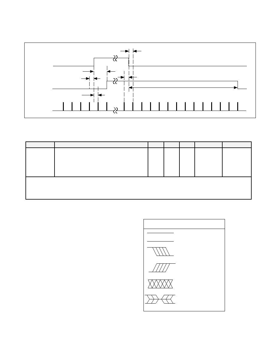
STEL-1109
30
PRELIMINARY PRODUCT INFORMATION
DATAEN TO DATAENO TIMING
WCP 52910.c-5/2/97
DATAEN
SYMPLS
tDIHDO
DATAENO
tDENSP
tSPDEN
tDLDO
tSPDEN
tDENSP
Table 28. DATAEN to DATAENO Timing AC Characteristics
(V
DD
= 3.3 V
±
10%, V
SS
= 0 V, T
a
= –40
∞
to 85
∞
C)
Symbol
Parameter
Min.
Nom.
Max.
Units
Conditions
t
DIHDO
DATAEN High to DATAENO High
2
nd
SYMPLS
Note 1
t
DLDO
DATAEN Low to DATAENO Low
13
th
SYMPLS
Note 1
t
SPDEN
SYMPLS (trailing edge) to DATAEN Setup
3
nsec
t
DENSP
DATAEN to SYMPLS (trailing edge) Setup
5
nsec
Notes:
1.
Shown for Configuration Register 36
H
, bit 6=0 (No Reed-Solomon). If bit 6 of Register 36
H
is a “1”, then the edges of
DATAENO will be delayed from those illustrated by 8, 4, or 2 SYMPLS for BPSK, QPSK, or 16QAM, respectively.
BURST TIMING EXAMPLES
The following seven timing diagrams are qualitative in
nature and meant to illustrate the functional
relationships between the control inputs and signal
outputs in various modes of burst operation. Use the
key at right to interpret the timing marks. Only the first
diagram is of a complete and realistic burst. The
remaining diagrams are too short in duration to show
DATAENO and CLKEN going low.
WCP 53036.c-5/6/97
WAVEFORM INPUTS OUTPUTS
Must be
Steady
Will be
Steady
May
Change
from H to L
Don't Care.
Any Change
Permitted
Will be
Changing
from H to L
May
Change
from L to H
Will be
Changing
from L to H
Changing.
State
Unknown
Does Not
Apply
Center
Line is High-
Impedance
"Off" State
Key:
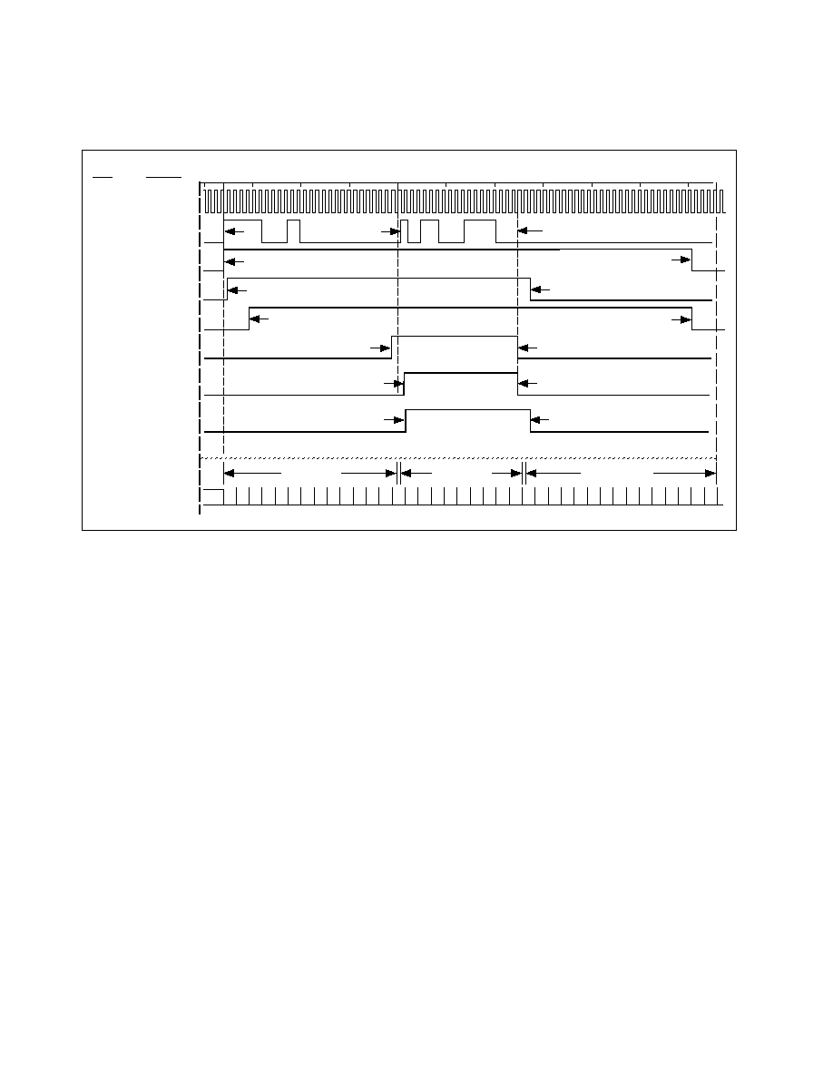
PRELIMINARY PRODUCT INFORMATION
31
STEL-1109
SLAVE MODE, QPSK
BURST TIMING: FULL BURST
WCP 52934.c -5/7/97
NAME
TCLK
(1)
TSDATA
CLKEN
DATAEN
DATAENO
(2)
DIFFEN
(3)
(B)
(F)
(E)
(I)
(G)
(H)
(A)
(C)
(D)
(J)
(K)
User Data
Guard Time
Preamble
PIN
19
17
26
18
39
70
RDSLEN
29
SCRMEN
32
SYMPLS
42
(L)
(M)
(L)
(N)
NOTES:
(1)
All input signals shown are derived from TCLK. Each edge is delayed from a TCLK edge by typically 6 to 18 nsec.
DATAENO does not depend on TCLK but its edges are synchronized to TCLK. TCLK itself can be turned off after DATAENI
goes low.
(2)
DATAENO shown at its minimum pipeline delay position. This is achieved by setting bit 6 of Configuration Register 36
H
to
zero. Reed-Solomon cannot be used in this mode. If bit 6 is set high, allowing Reed-Solomon an additional pipeline delay of
8
bits is inserted into the data path. This will shift both edges of DATAENO to the right by 8 cycles of TCLK.
(3)
If the preamble is not encoded the same as the user data, the DIFFEN control can be toggled in mid transmission as shown.
Otherwise, the DIFFEN control can be held high or low depending on encoding desired.
(A) First data bit transition on falling edge of TCLK (first of 14 preamble symbols). The data will be valid on the next rising edge of
TCLK.
(B) CLKEN rises on the same falling edge of TCLK that the data starts on. CLKEN is allowed to rise any time earlier than shown.
(C) DATAEN rises on the first rising edge of TCLK (middle of the first preamble bit).
(D) DATAENO rises on the falling edge of TCLK (at the end of the second symbol).
(E) DIFFEN rises on the rising edge of TCLK one symbol before the first user data symbol.
(F)
User data bits change on the falling edge of TCLK and must be valid during the next rising edge of TCLK.
(G) End of user data. Note that the data is allowed to go away immediately after it is latched in by the rising of TCLK which
occurs in the middle of the last user data bit.
(H) DIFFEN goes low on rising edge of TCLK (last user data symbol).
(I)
DATAEN goes low on rising edge of TCLK (on the cycle of TCLK after the last user data bit).
(J)
CLKEN must stay high until any time on or after the point where DATAENO goes low.
(K) DATAENO stays high until the 13th SYMPLS after DATAEN goes low.
(L) RDSLEN and SCRMEN go high on the first rising edge of TCLK in the User Data.
(M) RDSLEN goes low on the rising edge of TCLK (last user data symbol).
(N) SCRMEN goes low on the rising edge of TCLK (on the cycle of TCLK after the last user data bit).

STEL-1109
32
PRELIMINARY PRODUCT INFORMATION
MASTER MODE, BPSK
BURST TIMING SIGNAL RELATIONSHIPS
PI
PI
PI
PI
UI
UI
UI
UI
GI
GI
GI
GI
WCP 52911.c-5/6/97
CLKEN
BITCLK
TCLK
DATAEN
TSDATA
GUARD TIME
GUARD TIME
USER DATA
DIFFEN
RDSLEN
SCRMEN
SYMPLS
DATAENO
PREAMBLE
NOTE 1
NOTE 2
SLAVE MODE, BPSK
BURST TIMING SIGNAL RELATIONSHIPS
WCP 52912.c-5/6/97
CLKEN
BITCLK
TCLK
PI
PI
PI
PI
UI
UI
UI
UI
GI
GI
GI
GI
DATAEN
TSDATA
GUARD
TIME
GUARD TIME
USER DATA
DIFFEN
RDSLEN
SCRMEN
SYMPLS
DATAENO
PREAMBLE
NOTE 1
NOTE 2
NOTE 1:
STEL receivers differentially decode relative to the last preamble symbol. To encode the
first symbol against a "zero" symbol reference instead, bring DIFFEN high at the
leading edge of the user data packet (dotted line).
NOTE 2:
If bit 6 of Configuration Register 36
H
is a "1" then the rising edge of DATAENO will be
delayed by eight cycles of BITCLK (dotted line). This is required if the Reed-Solomon
encoder is used.
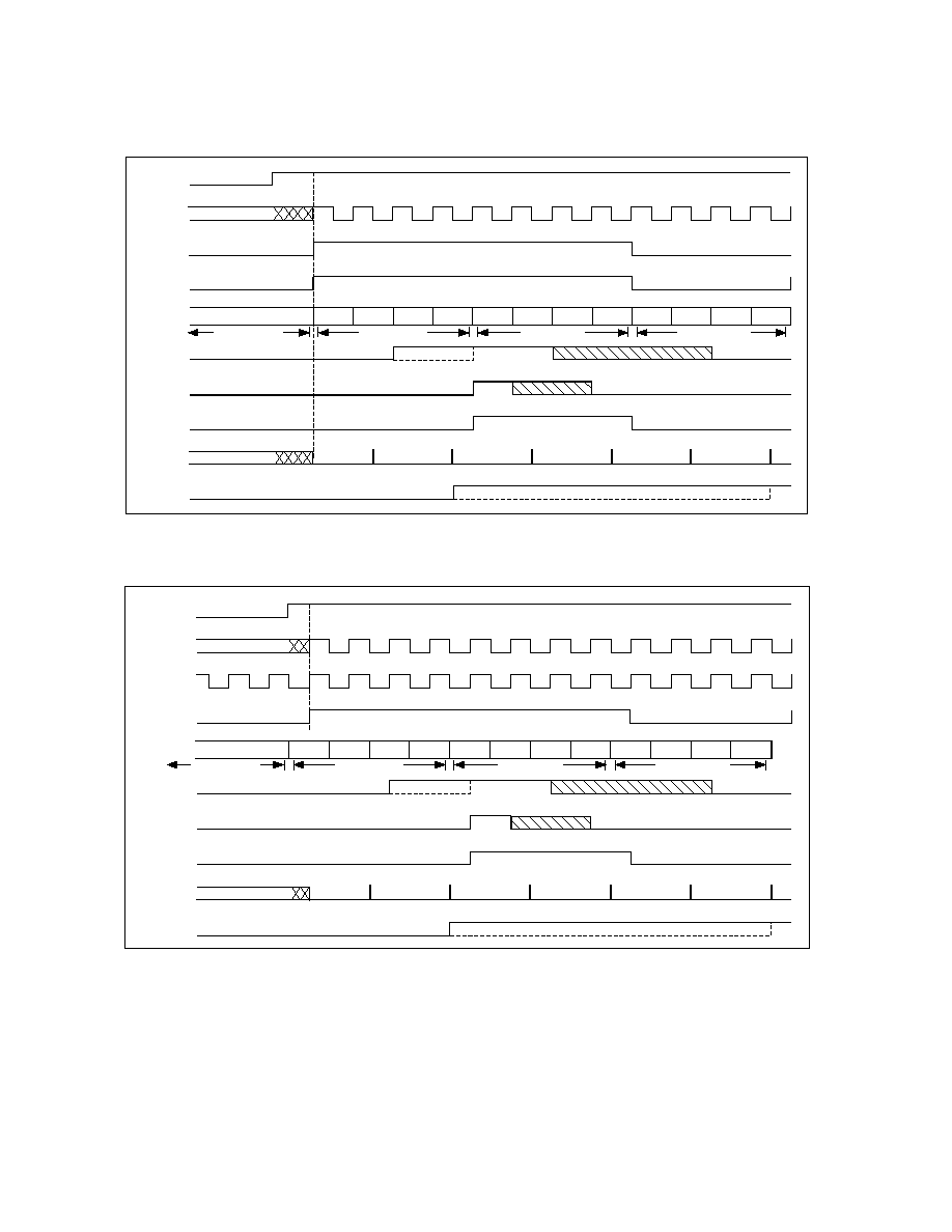
PRELIMINARY PRODUCT INFORMATION
33
STEL-1109
MASTER MODE, QPSK
BURST TIMING SIGNAL RELATIONSHIPS
CLKEN
BITCLK
TCLK
DATAEN
TSDATA
DIFFEN
RDSLEN
SCRMEN
SYMPLS
GUARD TIME
PI
PQ
PI
PQ
UI
UQ
UI
UQ
GI
GQ
GI
GQ
GUARD TIME
USER DATA
PREAMBLE
DATAENO
NOTE 1
WCP 52840.c-5/7/97
NOTE 2
SLAVE MODE, QPSK
BURST TIMING SIGNAL RELATIONSHIPS
CLKEN
BITCLK
TCLK
DATAEN
TSDATA
DIFFEN
RDSLEN
SCRMEN
SYMPLS
GUARD TIME
PI
PQ
PI
PQ
UI
UQ
UI
UQ
GI
GQ
GI
GQ
GUARD TIME
USER DATA
PREAMBLE
DATAENO
NOTE 2
NOTE 1
WCP 52839.c-5/7/97
NOTE 1:
STEL receivers differentially decode relative to the last preamble symbol. To encode the
first symbol against a "zero" symbol reference instead, bring DIFFEN high at the
leading edge of the user data packet (dotted line).
NOTE 2:
If bit 6 of Configuration Register 36
H
is a "1" then the rising edge of DATAENO will be
delayed by eight cycles of BITCLK (dotted line). This is required if the Reed-Solomon
encoder is used.

STEL-1109
34
PRELIMINARY PRODUCT INFORMATION
MASTER MODE, 16QAM
BURST TIMING SIGNAL RELATIONSHIPS
WCP 52913.c-5/6/97
CLKEN
TCLK
DATAEN
TSDATA
GUARD TIME
GUARD TIME
USER DATA
DIFFEN
RDSLEN
SCRMEN
DATAENO
PREAMBLE
BITCLK
SYMPLS
PI1 PQ1 PI0 PQ0 PI1 PQ1 PI0 PQ0 UI1 UQ1 UI0 UQ0 UI1 UQ1 UI0 UQ0 GI1 GQ1 GI0 GQ0 GI1 GQ1 GI0 GQ0
NOTE 1
NOTE 2
SLAVE MODE, 16QAM
BURST TIMING SIGNAL RELATIONSHIPS
WCP 52914.c-5/7/97
CLKEN
TCLK
DATAEN
TSDATA
GUARD TIME
GUARD TIME
USER DATA
DIFFEN
RDSLEN
SCRMEN
DATAENO
PREAMBLE
BITCLK
SYMPLS
PI1 PQ1 PI0 PQ0 PI1 PQ1 PI0 PQ0 UI1 UQ1 UI0 UQ0 UI1 UQ1 UI0 UQ0 GI1 GQ1 GI0 GQ0 GI1 GQ1 GI0 GQ0
NOTE 1
NOTE 2
NOTE 1:
STEL receivers differentially decode relative to the last preamble symbol. To encode the
first symbol against a "zero" symbol reference instead, bring DIFFEN high at the
leading edge of the user data packet (dotted line).
NOTE 2:
If bit 6 of Configuration Register 36
H
is a "1" then the rising edge of DATAENO will be
delayed by eight cycles of BITCLK (dotted line). This is required if the Reed-Solomon
encoder is used.
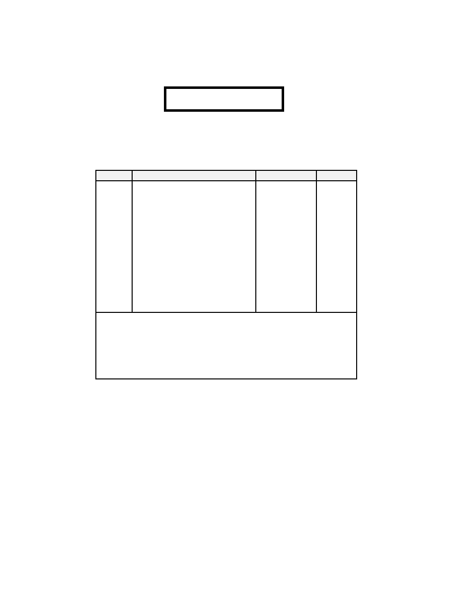
PRELIMINARY PRODUCT INFORMATION
35
STEL-1109
ELECTRICAL SPECIFICATIONS
The STEL-1109 electrical characteristics are provided by Table 29 through Table 31.
W
W
W
WA
A
A
AR
R
R
RN
N
N
NIIIIN
N
N
NG
G
G
G
Stresses greater than those shown in Table 29 may cause permanent damage to the
STEL-1109. Exposure to these conditions for extended periods may also affect the
STEL-1109’s reliability.
Table 29. Absolute Maximum Ratings
Symbol
Parameter
Range
Units
Note 1
T
stg
Storage Temperature
–40 to +125
∞
C
V
DDmax
Supply voltage on V
DD
–0.3 to +4.6
volts
AV
DDmax
Supply voltage on AV
DD
–0.3 to +4.6
volts
5V
DDmax
Supply voltage on 5V
DD
–0.3 to +7.0
volts
Note 2
AV
SS
Analog supply return for AV
DD
±
10% of V
DD
volts
V
I(max)
Input voltage
–0.3 to V
DD
+0.3
volts
I
i
DC input current
±
30
mA
P
Diss (max)
Power dissipation @ 85
o
C
690
mW
Note 3
Note:
1.
All voltages are referenced to VSS.
2. 5V
DD
must be greater than or equal to V
DD
. This rule can be violated for a
maximimum of 100 msec during power up.
3.
See Duty Cycle Derating Curves (Figure 15)
STEL-1109
36
PRELIMINARY PRODUCT INFORMATION
Ambient Temperature (degrees C)
100
90
80
70
60
50
25
30
35
40
45
50
55
60
65
70
75
80
85
Duty Cycle (%)
WCP 52994.c-4/26/97
Figure 15. Duty Cycle Derating versus Temperature (@3.3V)
Table 30. Recommended Operating Conditions
Symbol
Parameter
Range
NOTE 1
Units
AV
DD
Supply Voltage
+3.3
±
10%
volts
5V
DD
Supply Voltage
+5.0
±
10%
volts
Note 2
V
DD
Supply Voltage
+3.3
±
10%
volts
C
LOAD
DAC Load Capcitance
20
pF
R
LOAD
DAC Load Resistance
30K
ohms
Recommended DAC Load
37.5
ohms
V
LOAD
DAC Output Voltage
1.25
Volts
T
a
Operating Temperature (Ambient)
–40 to +85
∞
C
Note 3
Note:
1.
All voltages with respect to Vss and assume AV
SS
= V
SS
2.
If interface logic is to be driven by V
DD
then connect the 5V
DD
pin to the
V
DD
supply.
3.
Duty Cycle derating is required from +70 to +85 degrees.

PRELIMINARY PRODUCT INFORMATION
37
STEL-1109
Table 31. DC Characteristics
(V
DD
= 3.3 V +/-10%, V
SS
= 0 V, T
a
= -40
∞
to 85
∞
C)
Symbol
Parameter
Min.
Nom.
Max.
Units
Conditions
I
VDDQ
Supply Current, Quiescent
1.0
mA
Static, no clock
I
VDD
Supply Current, Operational, V
DD
1.9
mA/MHz
I5V
DD
Supply Current, Operational, 5V
DD
0.2
mA
IAV
DD
Supply Current, Operational, AV
DD
12.0
mA
VIH
CLK
Clock High Level Input Voltage
2.0
volts
CLK
, Logic '1'
VIL
CLK
Clock Low Level Input Voltage
0.8
volts
CLK
, Logic '0'
VIH
High Level Input Voltage
2.0
volts
Other inputs, Logic '1'
VIL
Low Level Input Voltage
0.8
volts
Other inputs, Logic '0'
IIH
High Level Input Current
10
µ
A
VIN = 5VDD
IIL
Low Level Input Current
–10
µ
A
VIN = VSS
VOH(min) High Level Output Voltage
2.4
3.0
VDD
volts
IO = –2.0 mA
VOL(max) Low Level Output Voltage
0.2
0.4
volts
IO = +2.0 mA
IOS
Output Short Circuit Current
NOTE 3
40
mA
VOUT = VDD,
VDD = max
CIN
Input Capacitance
2
pF
All inputs
COUT
Output Capacitance
4
10
pF
All outputs
I
OFS
Output Full Scale DAC Current
19.2
mA
V
O
DAC Compliance Voltage
(Differential)
±
0.96
Volts
R
O
DAC Output Resistance
TBD
Ohms
C
O
DAC Output Capacitance
TBD
pF
V
NO
DAC Output Noise Voltage Density
TBD
nV
Hz
NOTES:
1. With
V
SS
= AV
SS
, Noise coupling from supply to the DAC output.
2.
Noise coupling to DAC output when noise is common to AV
DD
and AV
SS
with respect to V
SS
of V
DD
and V
SS
with respect to
AV
SS
.
3.
Specified for digital outputs. The DAC output can survive an indefinite short circuit to AV
SS
.
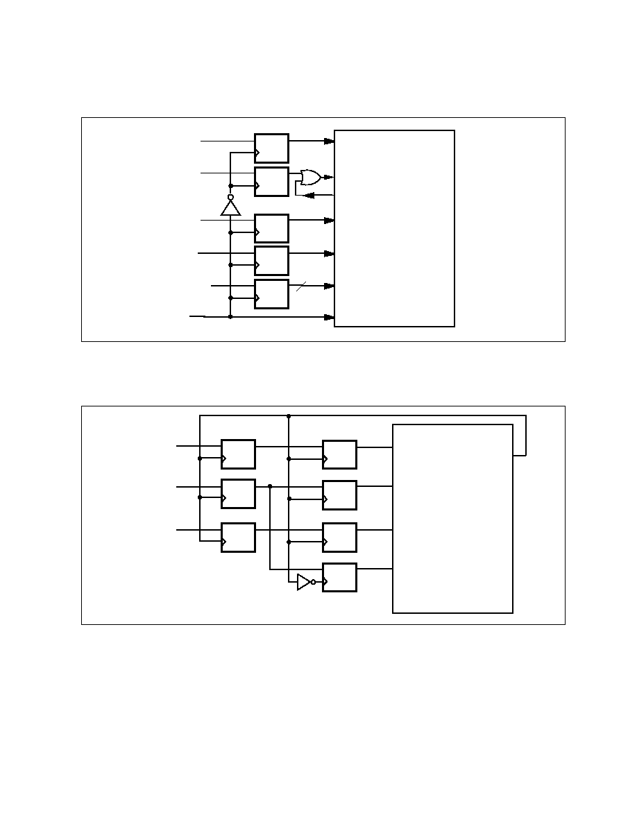
STEL-1109
38
PRELIMINARY PRODUCT INFORMATION
RECOMMENDED INTERFACE CIRCUITS
SLAVE MODE INTERFACE
STEL-1109
TSDATA
D
DIFFEN
DATAEN
TCLK
CLKEN
Q
D
Q
D
Q
D
Q
D
Q
2
TSDATA
DIFFEN
DATAEN
TCLK
CLKEN
FCWSEL
1-0
DATAENO
WCP 52995.c-5/2/97
FCWSEL
1-0
OR
MASTER MODE INTERFACE
STEL-1109
TSDATA
D
Q
D
Q
D
Q
D
Q
DATAEN
DIFFEN
CLKEN*
BITCLK
TCLK
TSDATA
DIFFEN
DATAEN
D
Q
WCP 52115.c-5/2/96
D
Q
D
Q
* CLKEN may be turned off between bursts to conserve power as long as it is kept on until after
DATAENO goes low. Note that the BITCLK output goes inactive whenever CLKEN is low.
PRELIMINARY PRODUCT INFORMATION
39
STEL-1109
EXAMPLE OUTPUT LOAD SCHEMATIC
X
T1-6TKK81
0.1
50
50
50
load
50
line Note 1
0.1
0.1
Mini-
Circuits
1:1
Iout
Ioutn
WCP-52997.c-5/6/97
AV
SS
Pin
53
Pin
52
AV
SS
Note 1: Normally some application dependant alias filtering and
amplitude control appear at this point in the circuit.
MECHANICAL SPECIFICATIONS
The STEL-1109 is packaged as a single chip. The chip’s package style, dimensions, and pin identification are shown
in Figure 16.
Top View
Pin 1 Identifier
0.012"/0.018"
0.0315"
±
0.008"
65
64
80
1
40
41
24
25
0.130" max.
Package style: 80-pin MQFP.
Thermal coefficient,
ja = 58
∞
C/W
Detail of pins
0.01" max.
0.029"/
0.041"
0.677"
±
0.008"
0.551"
±
0.008"
0.787"
±
0.008"
0.913"
±
0.008"
WCP 52998.c-4/26/97
Note:
Tolerance on pin spacing is not cumulative
Figure 16. STEL-1109 Mechanical Characteristics

WCP 970156
Copyright © Intel Corporation, December 15, 1999.
All rights reserved
Information in this document is provided in connection with
IntelÆ products. No license, express or implied, by estoppel
or otherwise, to any intellectual property rights is granted by
this document. Except as provided in Intels Terms and Con-
ditions of Sale for such products, Intel assumes no liability
whatsoever, and Intel disclaims any express or implied
warranty, relating to sale and/or use of IntelÆ products in-
cluding liability or warranties relating to fitness for a particu-
lar purpose, merchantability, or infringement of any patent,
copyright or other intellectual property right. Intel products
are not intended for use in medical, life saving, or life sus-
taining applications.
Intel may make changes to specifications and product de-
scriptions at any time, without notice.
For Further Information Call or Write
INTEL CORPORATION
Cable Network Operation
350 E. Plumeria Drive, San Jose, CA 95134
Customer Service Telephone: (408) 545-9700
Technical Support Telephone: (408) 545-9799
FAX: (408) 545-9888