Document Outline
- FEATURES
- FUNCTIONAL DESCRIPTION
- BLOCK DIAGRAM
- PIN CONFIGURATION
- FUNCTION BLOCK DESCRIPTION
- INPUT SIGNALS
- OUTPUT SIGNALS
- NCO RESET SEQUENCE
- ELECTRICAL CHARACTERISTICS
- ABSOLUTE MAXIMUM RATINGS
- RECOMMENDED OPERATING CONDITIONS
- D.C. CHARACTERISTICS
- A.C. CHARACTERISTICS
- NCO PHASE CHANGE SEQUENCE
- NCO FREQUENCY CHANGE SEQUENCE
- APPLICATIONS INFORMATION
- APPLICATIONS INFORMATION
- SPECTRAL PURITY
- TYPICAL SPECTRUM

R
STEL-1178A
Data Sheet
STEL-1178A
Dual 32-Bit Resolution
CMOS Phase Modulated
Numerically
Controlled Oscillator
STEL-1178A
2
FEATURES
s
TWO COMPLETELY INDEPENDENT
NCOs IN A SINGLE PACKAGE
s
80 MHz MAXIMUM CLOCK FREQUENCY
s
32-BIT FREQUENCY RESOLUTION
≠ 19 milli-Hz @ 80 MHz
s
WIDE OUTPUT BANDWIDTH
≠ 0 TO 32 MHz @ 80 MHz CLOCK
s
3-BIT PHASE MODULATION
s
SINE OR COSINE SIGNAL GENERATION
≠ 12-BIT OUTPUTS
s
HIGH SPECTRAL PURITY
≠ ALL SPURS < -75 dBc
s
MICROPROCESSOR COMPATIBLE
INPUTS
s
PROPRIETARY NOISE-REDUCTION
TECHNIQUES UTILIZED
s
68 PIN PLCC AND CLDCC PACKAGES
FUNCTIONAL DESCRIPTION
The STEL-1178A features two completely
independent 32-bit Numerically Controlled
Oscillators in a single package operating at up to 80
MHz. It provides a compact, low-cost solution to
applications requiring two independently controlled
precision frequency sources. Separate registers control
the functions of the two NCOs, making the device
very easy to program. In the STEL-1178A the two
NCOs also have independent 3-bit phase modulation,
making the device suitable for phase modulation
applications as well as making it possible to use an
STEL-1178A as a quadrature synthesizer. The two
NCOs also have independent clocks. The 12-bit
outputs provide ≠75 dBc purity with suitable DACs,
and DAC strobe outputs are also provided to simplify
DAC timing. The STEL-1178A uses digital techniques
to provide a cost-effective solution for low noise signal
sources. The dual NCO features high frequency
resolution with exceptional spectral purity of outputs
up to 32 MHz. The device combines low power 1.5
µ
CMOS technology with a unique architectural design
resulting in a power efficient, high-speed dual
sinusoidal waveform generator able to achieve fine
tuning resolution and exceptional spectral purity at
clock frequencies up to 80 MHz. The dual NCO is
designed to provide a simple interface to an 8-bit
microprocessor bus.
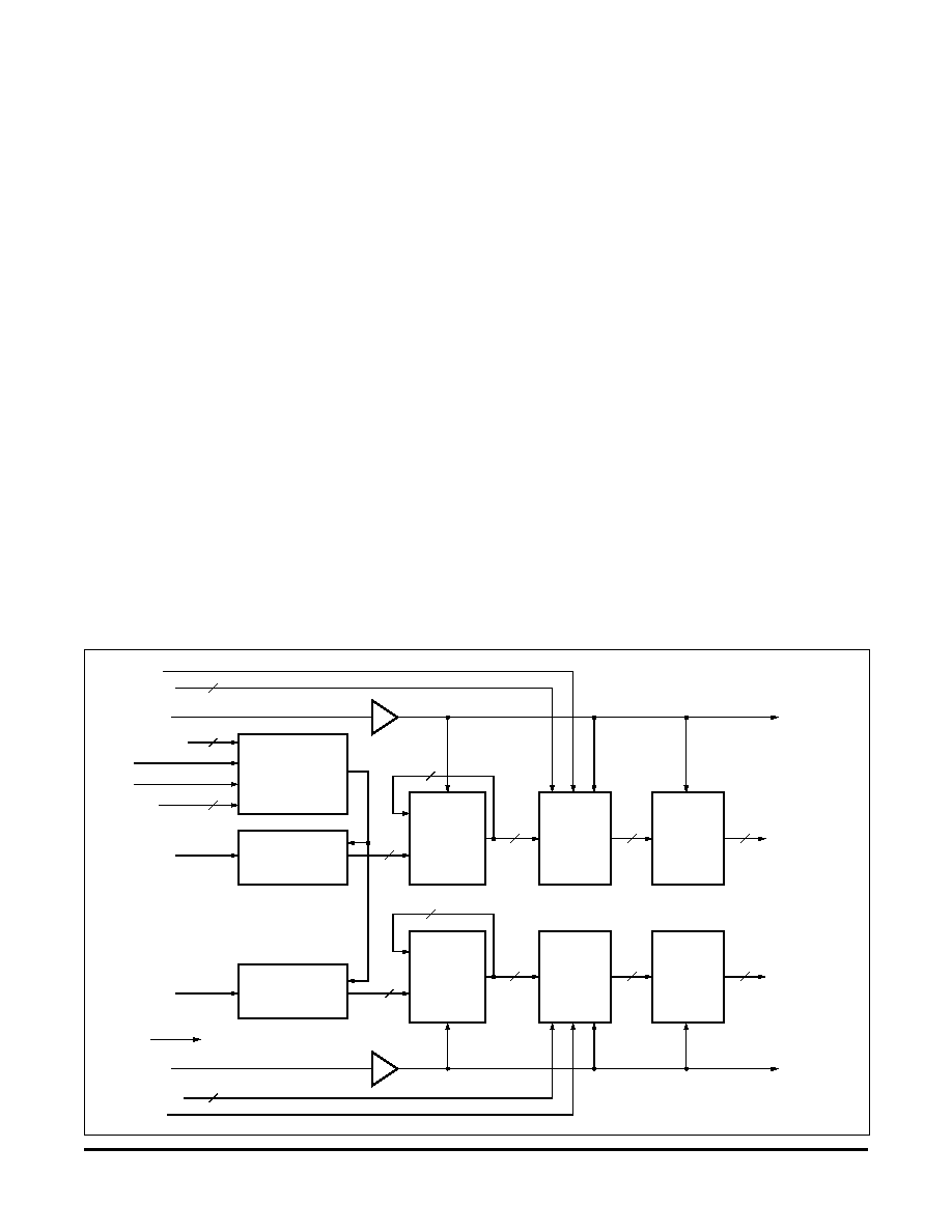
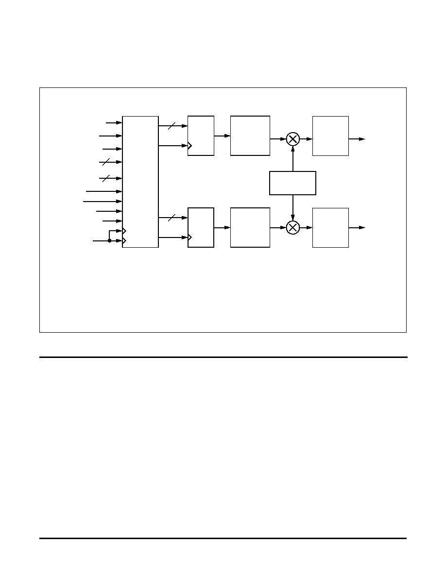
BLOCK DIAGRAM
RESET
(TO ALL REGISTERS)
ADDRESS
C S\
WR\
ADDRESS
SELEC T
LOGIC AND
BUFFER
REGISTER
DATA
-PHASE
REGISTER
A
-PHASE
REGISTER
B
PHASE
AC C UM-
ULATOR
HOP C LK1
32
SINE
LUT
13
12
DAC 1 BIT
32
PHASE
AC C UM-
ULATOR
32
SINE
LUT
13
12
DAC 2 BIT
32
DAC 1 STB
DAC 2 STB
SYSC LK1
SYSC LK2
HOP C LK2
11-0
11-0
7-0
5-0
5
8
PHASE
ALU
13
PHASE
ALU
13
PM1 BIT
PM1 C LK
3
2-0
PM2 BIT
PM2 C LK
3
2-0
3
STEL-1178A
0.145"
max.
0.990"
±
0.010"
0.035"
nomina
0.951"
±
0.009"
6 6 6 6 6 6 6 6
9 8 7 6 5 4 3 2 1 8 7 6 5 4 3 2 1
60
59
58
57
56
55
54
53
52
51
50
49
48
47
46
45
44
2 2 2 3 3 3 3 3 3 3 3 3 3 4 4 4 4
7 8 9 0 1 2 3 4 5 6 7 8 9 0 1 2 3
10
11
12
13
14
15
16
17
18
19
20
21
22
23
24
25
26
60
59
58
57
56
55
54
53
52
51
50
49
48
47
46
45
44
2 2 2 3 3 3 3 3 3 3 3 3 3 4 4 4 4
7 8 9 0 1 2 3 4 5 6 7 8 9 0 1 2 3
6 6 6 6 6 6 6 6
9 8 7 6 5 4 3 2 1 8 7 6 5 4 3 2 1
10
11
12
13
14
15
16
17
18
19
20
21
22
23
24
25
26
0.200"
max.
0.990"
±
0.005"
TOP
VIEW
0.05" (1)
0.017"
±
0.004" (2)
0.954"
±
0.004"
The sine functions are generated from the 13 most
significant bits of the phase accumulators. The
frequency of each NCO is determined by the number
stored in the
-Phase Register, which may be
programmed by an 8-bit microprocessor.
Each NCO generates a sampled sine wave where the
sampling function is the clock. The practical upper
limit of the NCO output frequency is about 40% of the
clock frequency due to spurious components that are
created by sampling. Those components are at
frequencies greater than half the clock frequency, and
become more difficult to remove by filtering.
Each NCO maintains a record of phase which is
accurate to 32 bits. At each clock cycle the number
stored in the 32-bit
-Phase register is added to the
previous value of the phase accumulator. The number
in the phase accumulator represents the current phase
of the synthesized sine function. The number in the
-
Phase register represents the phase change for each
cycle of the clock. This number is directly related to
the output frequency by the following:
f
c
x
-Phase
f
o
=
2
32
where: f
o
is the frequency of the output signal
and: f
c
is the clock frequency.
Notes: (1) Tolerances on pin spacing are not cumulative.
(2) Dimensions apply at seating plane.
(3) PLCC and CLDCC packages have different corners and may not fit into sockets designed
for the other type. Universal sockets are available without alignment locators.
Package: 68 pin CLDCC
Thermal coefficient,
ja
= 34
∞
C/W
Package: 68 pin PLCC
Thermal coefficient,
ja
= 36
∞
C/W
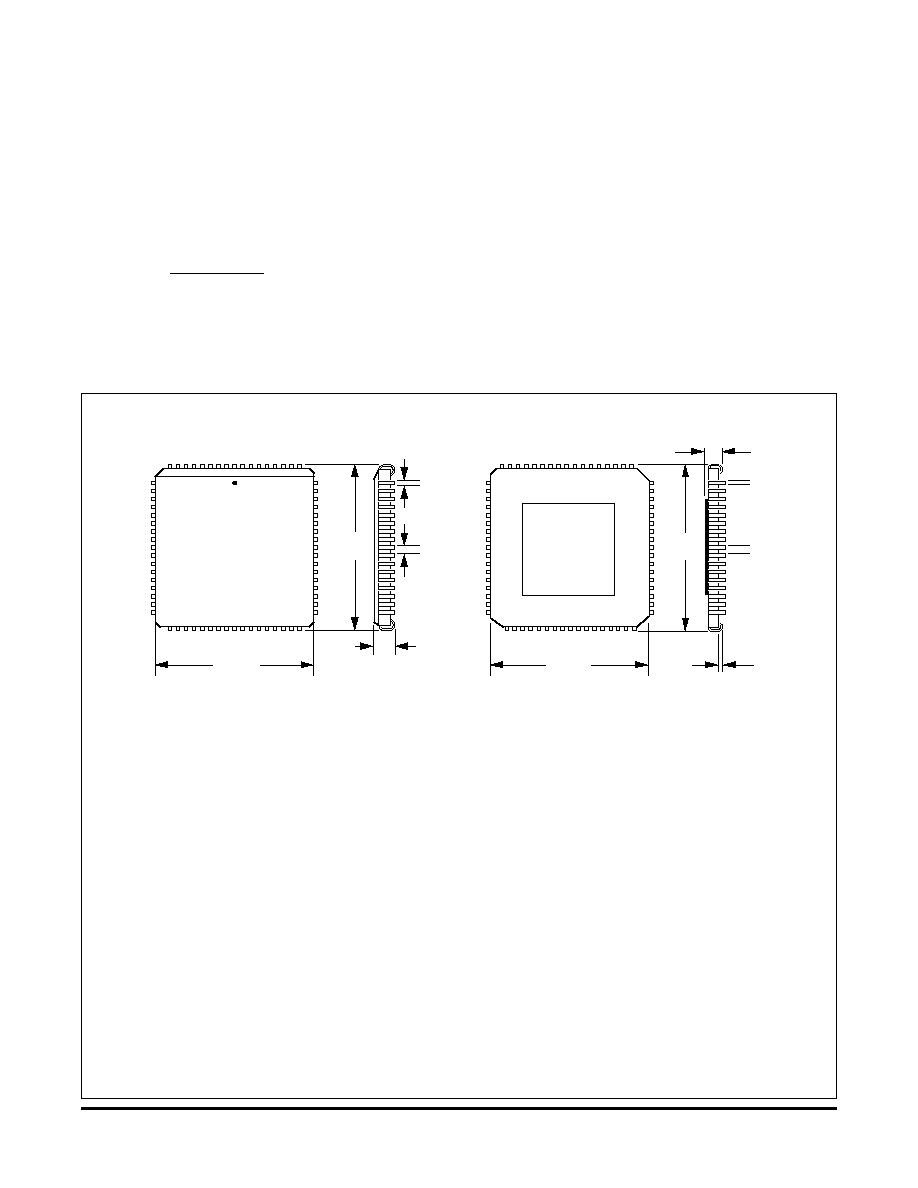
PIN CONNECTIONS
1
SYS CLK2
2
V
SS
3
ADDRESS
0
4
ADDRESS
3
5
ADDRESS
2
6
DATA
0
7
DATA
1
8
DATA
2
9
DATA
3
10 V
SS
11 DAC1 BIT11 (MSB)
12 DAC1 BIT
10
13 DAC1 BIT
9
14 DAC1 BIT
8
15 DAC1 BIT
7
16 DAC1 BIT
6
17 V
SS
18 V
DD
19 DAC1 BIT
5
20 DAC1 BIT
4
21 DAC1 BIT
3
22 DAC1 BIT
2
23 DAC1 BIT
1
24 DAC1 BIT0 (LSB)
25 V
SS
26 DAC1 STB
27 PM1 BIT
2
28 PM1 BIT
1
29 PM1 BIT
0
30 PM1 CLK
31 N.C
32 N.C
33 V
DD
34 HOP CLK1
35 SYS CLK1
36 CS\
37 WR\
38 ADDRESS
4
39 ADDRESS
1
40 DATA
7
41 DATA
6
42 DATA
5
43 DATA
4
44 V
SS
45 DAC2 BIT11
(MSB)
46 DAC2 BIT
10
47 DAC2 BIT
9
48 DAC2 BIT
8
49 DAC2 BIT
7
50 DAC2 BIT
6
51 V
SS
52 V
DD
53 DAC2 BIT
5
54 DAC2 BIT
4
55 DAC2 BIT
3
56 DAC2 BIT
2
57 DAC2 BIT
1
58 DAC2 BIT
0
59 RESET
60 DAC2 STB
61 PM2 BIT
2
62 PM2 BIT
1
63 PM2 BIT
0
64 PM2 CLK
65 N.C.
66 N.C.
67 V
DD
68 HOP CLK2
Notes: I.C. denotes Internal Connection. Do not use for vias.
N.C. denotes No Connection. May be used for vias.
TOP
VIEW
PIN CONFIGURATION

STEL-1178A
4
SINE LOOKUP TABLE BLOCKS 1 AND 2
These blocks are the sine memories. The 13 most
significant bits from the Phase Accumulator Blocks are
used to address these memories to generate the 12-bit
DAC1 BIT
11-0
and DAC2 BIT
11-0
outputs.
INPUT SIGNALS
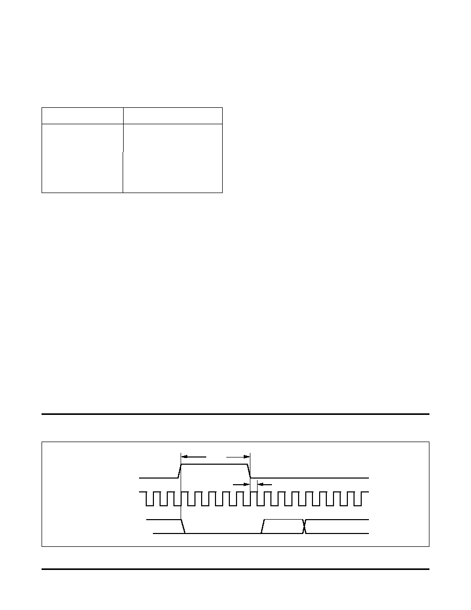
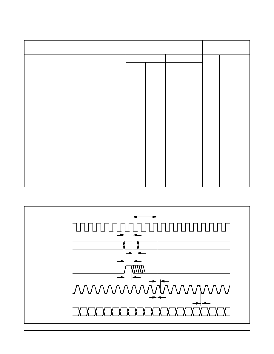
RESET
The RESET input is asynchronous and active high,
and clears all the registers in the device. When RESET
goes high all registers are cleared within 20 nsecs, and
normal operation will resume after this signal returns
low. The data on the outputs will then be invalid for 4
clock cycles, and thereafter will remain at the value
corresponding to zero phase until new frequencies are
loaded with the HOP CLK1/2 inputs after the RESET
returns low. The individual accumulators can be reset
(to set them to zero phase) without resetting the other
circuits by means of the Accumulator Reset software
command (ARST1 or 2), by writing dummy data into
addresses 0C
H
(NCO1) or 1C
H
(NCO2) as shown in
the address table. This will arm the corresponding
ARST function so that at the next HOP CLK command
(hardware or software) the accumulator will reset to
zero phase when the frequency change occurs.
SYS CLK1, SYS CLK2
All synchronous functions performed within the
NCOs are referenced to the falling edges of the
corresponding SYS CLK input. The SYS CLK1 and
SYS CLK2
signals should be nominally a square wave
at a maximum frequency of 80 MHz. Non-repetitive
SYS CLK1/2
waveforms are permissible as long as the
minimum duration positive or negative pulse on the
waveforms are always greater than 4 nanoseconds
(commercial).
CS\
The Chip Select input is used to control the writing of
data into the chip. It is active low. When this input is
high all data writing via the DATA
7-0
bus is inhibited.
WR\
The Write Strobe input is used to latch the data on the
DATA
7-0
bus into the device. On the rising edge of the
WR\
input, the information on the 8-bit data bus is
transferred to the buffer register selected by the
ADDR
3-0
bus.
DATA
7
through DATA
0
The 8-bit DATA
7-0
bus is used to program the two 32-
bit
-Phase Registers. DATA
0
is the least significant
bit of the bus. The data programmed into the
-Phase
Registers in this way determines the output
frequencies of the NCOs.
The phase noise of the NCO output signal may be
determined from the phase noise of the clock signal
input and the ratio of the output frequency to the clock
frequency. This ratio squared times the phase noise
power of the clock specified in a given bandwidth is
the phase noise power that may be expected in that
same bandwidth relative to the output frequency.
Each NCO achieves its high operating frequency by
making extensive use of pipelining in its architecture.
The pipeline delays within the NCOs represent 16
clock edges. Note that when frequency changes occur
at the outputs the changes are instantaneous, i.e., they
occur in one clock cycle, with complete phase
continuity.
FUNCTION BLOCK DESCRIPTION
ADDRESS SELECT LOGIC BLOCK
This block controls the writing of data into the device
via the DATA
7-0
inputs. The data is written into the
device on the rising edge of the WR\ input, and the
register into which the data is written is selected by
the ADDRESS
4-0
inputs. The CS\ input can be used
to selectively enable the writing of data from the bus.
-PHASE BUFFER REGISTER BLOCK
The
-Phase Buffer Register is used to temporarily
store the
-Phase data written into the device. This
allows the data to be written asynchronously as four
bytes per 32-bit
-Phase word. The data is transferred
from these registers into the
-Phase Registers after a
falling edge on the HOP CLK1 or HOP CLK2 inputs.
-PHASE REGISTER BLOCKS 1 AND 2
These blocks control the updating of the
-Phase
words used in the Accumulators. The frequency data
from the Buffer Register Block is loaded into these
blocks after a falling edge on the HOP CLK1 or HOP
CLK2
inputs.
PHASE ACCUMULATOR BLOCKS 1 AND 2
These blocks form the core of the dual NCO function.
They are high-speed, pipelined, 32-bit parallel
accumulators, generating a new sum in every clock
cycle. The overflow signal is discarded, since the
required output is the modulo (2
32
) sum only. This
represents the modulo(2
) phase angle.
PHASE ALU BLOCKS 1 AND 2
These blocks perform the modulation of the outputs
of the Phase Accumulators with the modulation
signals PM1 BIT
2-0
and PM2 BIT
2-0
. These 3-bit signals
allow the outputs of the NCOs to be modulated
independently to generate a variety of signal types.
5
STEL-1178A
ADDR
4
through ADDR
0
The five address lines ADDR
4-0
control the use of the
DATA
7-0
bus for writing frequency data to the
-
Phase Buffer Registers, as shown in the tables. When
ADDR
4
is set low all input data will program NCO1 ,
and when it is set high the data will program NCO2:
ADDR
3
- ADDR
0
Register Field
0
0
0
0
-Phase Bits 7 ≠0(LSB)
0
0
0
1
-Phase Bits15 ≠ 8
0
0
1
0
-Phase Bits 23 ≠ 16
0
0
1
1
-Phase Bits 31 ≠ 24
1
1
0
0
ARST1 or ARST2
1
1
1
0
HOP CLK1 or HOP CLK2
Addresses 0C
H
, 0E
H
, 1C
H
and 1E
H
do not contain
physical registers. The functions will be performed
whenever any data values are written into these
addresses. The remaining unspecified addresses do
not contain any physical registers and do not perform
any functions. When changing frequency data it is not
necessary to reload unchanged bytes, and the byte
loading sequence may be random.
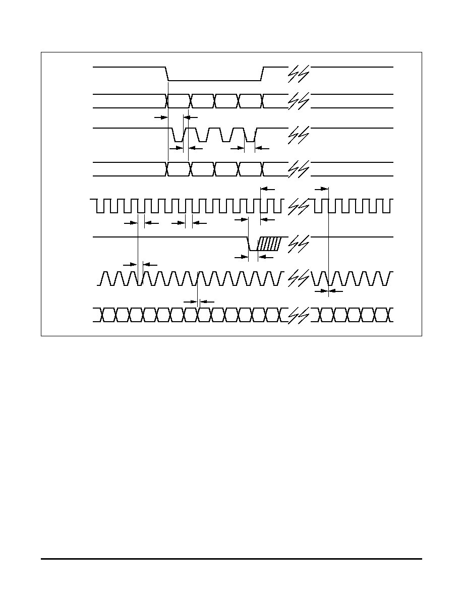
HOP CLK1 and HOP CLK2
The HOP CLK inputs are used to control the transfer
of the data from the
-Phase Buffer Registers to the
-
Phase Registers. The frequency of the NCO output
will change 16 falling clock edges after the
corresponding
HOP CLK
command due to pipelining
delays. The maximum frequency update rate is once
every 8 SYS CLK1/2 cycles. The HOP CLK function
can also be controlled by means of the FRLD software
command by writing dummy data to address 0E
H
(NCO1) or 1E
H
(NCO2), as shown in the address table.
PM1 BIT
2-0
and PM2 BIT
2-0
The two 3-bit inputs PM1 BIT
2-0
and PM2 BIT
2-0
are
used to phase modulate NCO1 and NCO2
respectively. The MSB of each input (PM1/2 BIT
2
)
corresponds to a 180
∞
phase shift at each output.
PM1 CLK and PM2 CLK
The PM1/2 CLK inputs are used to load the signals
into the Phase ALUs. The phase of the NCO output
will change 4 falling clock edges after the
corresponding PM1/2 CLK command due to
pipelining delays. The maximum phase update rate is
once every 2 SYS CLK cycles.
OUTPUT SIGNALS
DAC1 BIT
11-0
and DAC2 BIT
11-0
The signals appearing on the DAC1 BIT
11-0
and DAC2
BIT
11-0
output busses are derived from the 13 most
significant bits of the corresponding Phase
Accumulator. The 12-bit sine functions are presented
in offset binary format. The value of the output for a
given phase value follows the relationship:
DAC BIT
11-0
=2047 x sin (360 x (phase + 0.5)/8192)
∞
+
2048
The result is accurate to within 1 LSB. When the phase
accumulator is zero, e.g., after a reset, the decimal
value of the output is 2049 (801
H
).
DAC1 STB and DAC2 STB
The DAC Strobe outputs are used to clock the digital
to analog converters (DACs) used with the STEL-
1178A for optimum timing. The DAC1 BIT
11-0
and DAC2 BIT
11-0
signals change on the falling edges
of the corresponding DAC1/2 STB.
NCO RESET SEQUENCE
DAC BIT
11-0
801
H
t
RS
NOT VALID
RESET
SYSCLK
1
2
3
4
t
SR
STEL-1178A
6
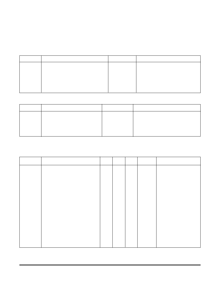
ELECTRICAL CHARACTERISTICS
ABSOLUTE MAXIMUM RATINGS
Warning: Stresses greater than those shown below may cause permanent damage to the
device. Exposure of the device to these conditions for extended periods may also affect de-
vice reliability. All voltages are referenced to V
ss
.
Symbol
Parameter
Range
Units
T
stg
Storage Temperature
≠40 to +125
∞
C (Plastic package)
≠65 to +150
∞
C (Ceramic package)
V
DDmax
Supply voltage on V
DD
≠0.3 to + 7
volts
V
I(max)
Input voltage
≠0.3 to V
DD
+0.3 volts
I
i
DC input current
±
10
mA
RECOMMENDED OPERATING CONDITIONS
Symbol
Parameter
Range
Units
V
DD
Supply Voltage
+5
±
5%
Volts
(Commercial Conditions)
+5
±
10%
Volts
(Military Conditions)
T
a
Operating Temperature (Ambient)
0 to +70
∞
C
(Commercial Conditions)
≠55 to +125
∞
C
(Military Conditions)
D.C. CHARACTERISTICS
(Operating Conditions: V
DD
= 5.0 V
±
5%, V
SS
=0 V, T
a
= 0
∞
to 70
∞
C, Commercial
V
DD
= 5.0 V
±
10%, V
SS
=0 V, T
a
=≠55
∞
to 125
∞
C, Military
Symbol
Parameter
Min. Typ. Max.
Units
Conditions
I
DD(Q)
Supply Current, Quiescent
1.0 mA
Static, no clock
I
DD
Supply Current, Operational
2.0 mA/MHz f
CLK
= 80 MHz, each NCO
V
IH(min)
High Level Input Voltage
Commercial Operating Conditions
2.0
volts
Logic '1'
Military Operating Conditions
2.25
volts
Logic '1'
V
IL(max)
Low Level Input Voltage
0.8 volts
Logic '0'
I
IH(min)
High Level Input Current
30
70
130
µ
A
CS\
, WR\, V
IN
= V
DD
I
IL(max)
Low Level Input Current
≠60
≠150
≠300
µ
A
All other inputs, V
IN
= V
SS
V
OH(min)
High Level Output Voltage
2.4
4.5
volts
I
O
= ≠4.0 mA
V
OL(max)
Low Level Output Voltage
0.2
0.4 volts
I
O
= +4.0 mA
I
OS
Output Short Circuit Current
20
65
130 mA
V
OUT
= V
DD
, V
DD
= max
≠10
≠45
≠130 mA
V
OUT
= V
SS
, V
DD
= max
C
IN
Input Capacitance
2
pF
All inputs
C
OUT
Output Capacitance
4
pF
All outputs
7
STEL-1178A
A.C. CHARACTERISTICS
(Operating Conditions: V
DD
= 5.0 V
±
5%, V
SS
=0 V, T
a
= 0
∞
to 70
∞
C, Commercial
V
DD
= 5.0 V
±
10%, V
SS
=0 V, T
a
=≠55
∞
to 125
∞
C, Military)
STEL-1178A+80
Commercial Military
Symbol Parameter
Min. Max. Min.
Max. Units Conditions
t
RS
RESET
pulse width
20
25
nsec.
t
SR
RESET
to SYSCLK Setup
10
12
nsec.
t
SU
DATA
, ADDR or CS\
5
6
nsec.
to WR\ Setup, and HOP CLK
or PM CLK to SYS CLK Setup
t
HD
DATA
, ADDR or CS\
5
6
nsec.
to WR\ Hold, and HOP CLK
or PM CLK to SYS CLK Hold
t
CH
SYS CLK
high
4
5
nsec.
f
CLK
= max.
t
CL
SYS CLK
low
4
5
nsec.
f
CLK
= max.
t
W
WR\
, HOP CLK, PM CLK
10
12
nsec.
pulse width
t
CS
SYS CLK
to DAC STB delay
4 17
3
20
nsec.
Load = 15 pF
(All outputs)
t
SD
DACSTB
to DAC BIT delay
1 3
1
5
nsec.
Load = 15 pF
(All outputs)
NCO PHASE CHANGE SEQUENCE
t
SU
PM BIT
2-0
DAC BIT
11-0
PM CLK
DAC STB
SYSCLK
DON'T CARE
4 CLOCK EDGES
OLD PHASE
NEW PHASE
DON'T CARE
t
HD
t
SU
t
W
t
CS
t
SD
STEL-1178A
8
NCO FREQUENCY CHANGE SEQUENCE
APPLICATIONS INFORMATION
Requirements for using an STEL-1178A NCO
in an application designed for the STEL-1178
The STEL-1178A is an enhanced version of the
STEL-1178 Dual NCO; the enhancement is the
addition of 3-bit phase modulation to the two NCOs.
As long as the phase modulation function is not
inadvertently operated it is possible to use an STEL-
1178A in an application that was designed around the
STEL-1178. This is easily achieved by meeting the
following criteria:
1.
Absolute minimum requirements for correct
operation:
The phase modulation is triggered by the PM1
CLK
and PM2 CLK signals on pins 30 and 64
respectively. As long as there are no active signals
connected to these edge triggered inputs an STEL-
1178A will operate in an identical manner to an
STEL-1178 in the system.
2.
For improved reliability of the STEL-1178A and its
operation in the system it is desirable that the pins
used for the phase modulation function in this
device should not be left floating. (This is true of all
unused inputs on CMOS devices.) This condition
will be met by connecting pins 27-30 and 61-64 to
either GND (V
SS
) or V
DD
. Since these pins are N.C.
(No Connection) on the STEL-1178 these
connections will not affect the operation of this
device in the system.
DATA
7-0
HOP CLK
WR\
CS\
ADDR
4-0
DON'T CARE
DON'T CARE
DON'T CARE
16 CLOCK
EDGES
OLD FREQUENCY
NEW FREQUENCY
DON'T CARE
t
SU
t
HD
t
WR
t
CH
t
CL
t
SU
t
W
DAC STB
SYS CLK
t
CS
t
SD
9
STEL-1178A
The STEL-1178A is ideally suited for modem applications since it can be used to synthesize signals
for both the transmitter and receiver sections simultaneously. In addition, the ability to modulate
the signals allows the NCO used in the transmitter synthesizer to be used as the PSK modulator as
well as the synthesizer. The NCO used in the receiver local oscillator synthesizer can be controlled
by the host processor to act as a tracking oscillator and to be phase locked to the incoming signal.
The sine or cosine signals generated by the STEL-
1178A have 12 bits of amplitude resolution and 13 bits
of phase resolution which results in spurious levels
which are theoretically at least 75 dB down. The
highest output frequency the NCO can generate is half
the clock frequency (f
c
/2), and the spurious
components at frequencies greater than f
c
/2 can be
removed by filtering. As the output frequency f
o
of the
SPECTRAL PURITY
In many applications the NCO is used with a digital
to analog converter (DAC) to generate an analog
waveform which approximates an ideal sinewave.
The spectral purity of this synthesized waveform is a
function of many variables including the phase and
amplitude quantization, the ratio of the clock
frequency to output frequency, and the dynamic
characteristics of the DAC.
APPLICATIONS INFORMATION
TYPICAL APPLICATION OF A DUAL NCO - TRANSMITTER PSK MODULATOR/
SYNTHESIZER AND RECEIVER LOCAL OSCILLATOR FOR A MODEM
DA TA
7-0
HOP CLK1
RESET
66-74 MHz
STEL-
1178A
DUA L
NCO
BPF
6-14
MHz
BPF
66-74
MHz
60 MHz
OSCILLA TOR
5
8
WR\
DA C
SY S
CLK
1 & 2
66-74 MHz
12
50-80 MHz
CLOCK
BPF
6-14
MHz
BPF
66-74
MHz
PM1 BIT
2-0
PM1 CLK
DA C
12
DA C1
BIT
11-0
HOP CLK2
DA C1
STB
DA C2
STB
CS\
PSK Tx
OUT
LO TO
MIXER
A DDR
4-0
DA C2
BIT
11-0

STEL-1178A
10
NCO approaches f
c
/2, the "image" spur at f
c
≠ f
o
(created by the sampling process) also approaches
f
c
/2 from above. If the programmed output frequency
is very close to f
c
/2 it will be virtually impossible to
remove this image spur by filtering. For this reason,
the maximum practical output frequency of the NCO
should be limited to about 40% of the clock frequency.
A spectral plot of the NCO output after conversion
with a DAC (Sony CX20202A-1) is shown below. In
this case, the clock frequency is 60 MHz and the output
frequency is programmed to 6.789 MHz. This 10-bit
DAC gives better performance than any of the
currently available 12-bit DACs at clock frequencies
higher than 10 or 20 MHz. The maximum non-
harmonic spur level observed over the entire useful
output frequency range in this case is ≠74 dBc. The
spur levels are limited by the dynamic linearity of the
DAC. It is important to remember that when the
output frequency exceeds 25% of the clock frequency,
the second harmonic frequency will be higher than the
Nyquist frequency, 50% of the clock frequency. When
this happens, the image of the harmonic at the
frequency f
c
≠ 2f
o
, which is not harmonically related to
the output signal, will become intrusive since its
frequency falls as the output frequency rises,
eventually crossing the fundamental output when its
frequency crosses through f
c
/3. It would be necessary
to select a DAC with better dynamic linearity to
improve the harmonic spur levels. (The dynamic
linearity of a DAC is a function of both its static
linearity and its dynamic characteristics, such as
settling time and slew rates.) At higher output
frequencies the waveform produced by the DAC will
have large output changes from sample to sample. For
this reason, the settling time of the DAC should be
short in comparison to the clock period. As a general
rule, the DAC used should have the lowest possible
glitch energy as well as the shortest possible settling
time.
TYPICAL SPECTRUM
Center Frequency:
6.7 MHz
Frequency Span:
10.0 MHz
Reference Level:
≠5 dBm
Resolution Bandwidth: 1 KHz
Video Bandwidth:
3 kHz
Scale:
Log, 10 dB/div
Output frequency:
6.789 MHz
Clock frequency:
60 MHz

Copyright © Intel Corporation, December 15, 1999.
All rights reserved
Information in this document is provided in connection with
IntelÆ products. No license, express or implied, by estoppel
or otherwise, to any intellectual property rights is granted by
this document. Except as provided in Intels Terms and Con-
ditions of Sale for such products, Intel assumes no liability
whatsoever, and Intel disclaims any express or implied
warranty, relating to sale and/or use of IntelÆ products in-
cluding liability or warranties relating to fitness for a particu-
lar purpose, merchantability, or infringement of any patent,
copyright or other intellectual property right. Intel products
are not intended for use in medical, life saving, or life sus-
taining applications.
Intel may make changes to specifications and product de-
scriptions at any time, without notice.
For Further Information Call or Write
INTEL CORPORATION
Cable Network Operation
350 E. Plumeria Drive, San Jose, CA 95134
Customer Service Telephone: (408) 545-9700
Technical Support Telephone: (408) 545-9799
FAX: (408) 545-9888