Document Outline
- FEATURES
- BENEFITS
- BLOCK DIAGRAM
- PACKAGE OUTLINE
- PIN CONFIGURATION
- GENERAL DESCRIPTION
- FUNCTIONAL BLOCKS
- INPUT SIGNALS
- OUTPUT SIGNALS
- CONTROL REGISTERS
- REGISTER SETTING SEQUENCE
- DECIMAL, HEX AND BINARY ADDRESS EQUIVALENTS
- REGISTER SUMMARY
- ELECTRICAL CHARACTERISTICS
- ABSOLUTE MAXIMUM RATINGS
- RECOMMENDED OPERATING CONDITIONS
- D.C. CHARACTERISTICS
- TRANSMITTER INPUT/OUTPUT TIMING
- A.C. CHARACTERISTICS
- RECEIVER INPUT/OUTPUT TIMING
- A.C. CHARACTERISTICS
- RXTEST BUS AND MICROPROCESSOR INTERFACE TIMING
- A.C. CHARACTERISTICS
- APPENDIX I: THEORY OF OPERATION
- APPENDIX II: TYPICAL APPLICATION

R
STEL-2000A
Data Sheet
STEL-2000A+45
(45 MHz)
STEL-2000A+20
(20 MHz)
Digital, Fast Acquisition
Spread Spectrum
Burst Processor

≠≠≠≠≠≠≠≠≠≠≠≠≠≠≠≠≠≠≠≠≠≠≠≠≠≠≠≠≠≠≠≠≠≠≠≠≠≠≠≠≠≠≠≠≠≠≠≠≠≠≠≠
STEL-2000A
2
FEATURES/BENEFITS .......................................................................................................................................
3
BLOCK DIAGRAM..............................................................................................................................................
3
PACKAGE OUTLINE..........................................................................................................................................
4
PIN CONFIGURATION......................................................................................................................................
4
GENERAL DESCRIPTION .................................................................................................................................
5
FUNCTIONAL BLOCKS.....................................................................................................................................
7
Transmit and Receive Clock Generator Blocks..................................................................................
7
Input and Output Processor Blocks ....................................................................................................
7
Differential Encoder Block....................................................................................................................
7
Transmitter PN Code Generator Block...............................................................................................
7
BPSK/QPSK Modulator Block.............................................................................................................
8
Frequency Control Register and NCO Block .....................................................................................
8
Downconverter Block............................................................................................................................
8
Receiver PN Code Register and PN Matched Filter Blocks.............................................................
9
Power Detector Block ............................................................................................................................
10
Symbol Tracking Processor Block........................................................................................................
11
Differential Demodulator Block ..........................................................................................................
11
Frequency Discriminator and Loop Filter Block ...............................................................................
12
INPUT SIGNALS..................................................................................................................................................
14
OUTPUT SIGNALS..............................................................................................................................................
18
TRANSMITTER AND RECEIVER TEST POINTS ..........................................................................................
20
CONTROL REGISTERS ......................................................................................................................................
21
Downconverter Registers......................................................................................................................
21
PN Matched Filter Registers.................................................................................................................
22
Power Estimator Registers....................................................................................................................
23
Acquisition and Tracking Processor Registers ..................................................................................
24
Demodulator Registers..........................................................................................................................
27
Output Processor Control Registers....................................................................................................
29
Transmit Control Registers...................................................................................................................
31
REGISTER SETTING SEQUENCE
........................................................................................................
33
DECIMAL, HEX AND BINARY ADDRESS EQUIVALENTS.......................................................................
34
REGISTER SUMMARY .......................................................................................................................................
35
ELECTRICAL CHARACTERISTICS .................................................................................................................
36
ABSOLUTE MAXIMUM RATINGS....................................................................................................
36
RECOMMENDED OPERATING CONDITIONS .............................................................................
36
D.C. CHARACTERISTICS....................................................................................................................
36
TRANSMITTER INPUT/OUTPUT TIMING ....................................................................................
37
RECEIVER INPUT/OUTPUT TIMING..............................................................................................
38
MICROPROCESSOR INTERFACE TIMING .....................................................................................
39
APPENDIX I: THEORY OF OPERATION ......................................................................................................
40
Digital Downconversion .......................................................................................................................
40
Using the STEL-2000A with a Single ADC in Direct I.F. Sampling Mode ...............................
40
Using the STEL-2000A with Two ADCs in Quadrature Sampling Mode ................................
43
Differential Demodulation ...................................................................................................................
44
BPSK Demodulation .........................................................................................................................
44
QPSK Demodulation ........................................................................................................................
44
Frequency Error Generation.................................................................................................................
45
Using the Modulator in the STEL-2000A Transmitter......................................................................
46
APPENDIX II: TYPICAL APPLICATION .......................................................................................................
48
≠≠≠≠≠≠≠≠≠≠≠≠≠≠≠≠≠≠≠≠≠≠≠≠≠≠≠≠≠≠≠≠≠≠≠≠≠≠≠≠≠≠≠≠≠≠≠≠≠≠≠≠
3
STEL-2000A
FEATURES
s
Complete direct sequence spread spectrum
burst transceiver in a single CMOS I.C.
s
Programmable functionality supports
many different operational modes
s
Supports PN chip rate of over 11
Mchips/sec. in transmit and receive modes
(STEL-2000A+45 only)
s
Acquires within one symbol duration
using digital PN Matched Filter
s
Two independent PN sequences, each up
to 64 chips long, for distinct processing of
the acquisition/preamble symbol and
subsequent data symbols
s
Power management features
s
Optional spectral whitening code
generation
s
Full or half duplex operation
s
100-Pin PQFP packaging
BENEFITS
s
High performance and high reliability
with reduced manufacturing costs
s
Ideal for a wide range of wireless
applications including data acquisition
systems, transaction systems and wireless
Local Area Networks (WLANs)
s
Supports data rates up to 2.048 Mbps in
compliance with FCC regulations
(STEL-2000A+45 only)
s
Fast response and very low overhead when
operating in burst modes
s
Allows high processing gain to maximize
the acquisition probability, then reduced
code length for increased data rate
s
Low power consumption
s
Randomizes data to meet regulatory
requirements
s
Permits dual frequency (Frequency
Division Duplex) or single frequency
(Time Division Duplex) operation
s
Small footprint, surface mount
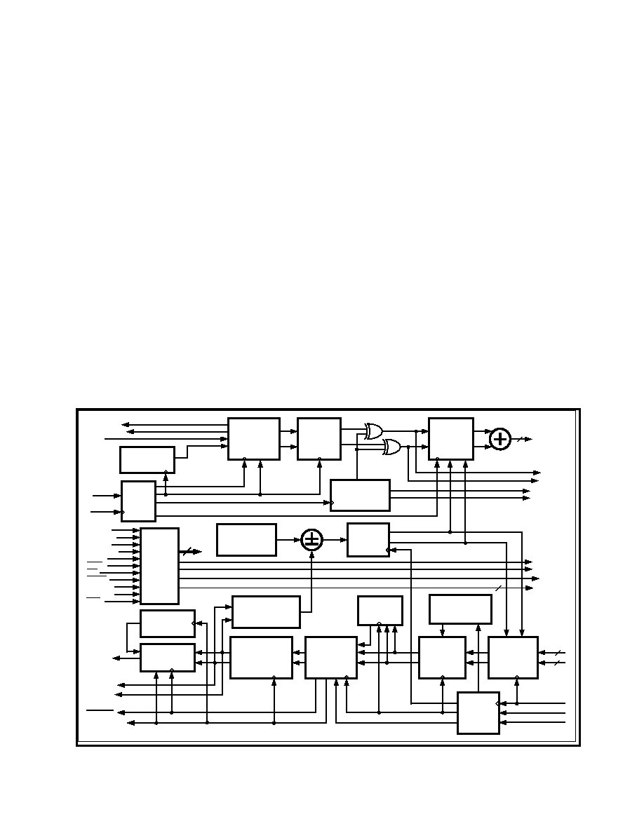
BLOCK DIAGRAM
(Figure 1)
TX
CLOCK
GENER-
ATOR
OUTPUT DATA
PROCESSOR
DIFFER-
ENTIAL
ENCODER
TX PN CODE
GENERATORS
QPSK
MODU-
LATOR
BIT CLOCK
SYMBOL CLOCK
CHIP CLOCK
TXIFCLK
NCO
DOWN
CONVERTER
MATCHED
FILTER
POWER
DETECTOR
SYMBOL
TRACKING
PROCESSOR
RX
CLOCK
GENER-
ATOR
SYMBOL CLOCK
CORRECTED BIT CLOCK
CORRECTED SYMBOL CLOCK
FREQUENCY
DISCRIMINATOR
& LOOP FILTER
SIN
COS
FREQUENCY
CONTROL
REGISTER
2x CHIP CLOCK
DIFFERENTIAL
DEMODULATOR
RX PN CODE
REGISTERS
CHI
P
CL
O
C
K
RXMABRT
MNCOEN
MTXEN
MRXEN
MFLD
DATA
7-0
ADDR
6-0
CONTROL
& µP
INTER-
FACE
RESET
WR
CSEL
TXIFCLK
TXIN
TXBITPLS
TXTRKPLS
TXMCHP
TXIFOUT
7-0
TXIOUT
TXQOUT
TXCHPPLS
TXACQPLS
RXIIN
7-0
RXQIN
7-0
RXIFCLK
RXMSMPL
RXMDET
RXOUT
RXIOUT
RXQOUT
RXDRDY
RXSYMPLS
RXACTIVE
TXACTIVE
TX OVERLAY
CODE
GENERATOR
RX OVERLAY
CODE
GENERATOR
TXTEST
RXTEST
7-0
OEN
RXIFCLK
INPUT DATA
PROCESSOR
≠≠≠≠≠≠≠≠≠≠≠≠≠≠≠≠≠≠≠≠≠≠≠≠≠≠≠≠≠≠≠≠≠≠≠≠≠≠≠≠≠≠≠≠≠≠≠≠≠≠≠≠
STEL-2000A
4
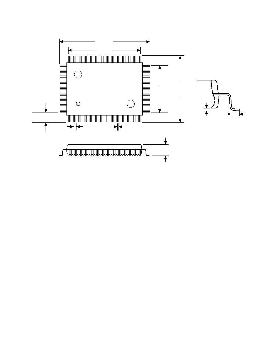
PACKAGE OUTLINE
(Figure 2)
Top View
0.941"
±
0.010"
0.742"
±
0.005"
0.487"
±
0.003"
0.705"
±
0.010"
0.11" nom.
0.122" max.
0.014"
±
0.002"
0.0256"
±
0.002"
0.031"
±
0.005"
0.009"
±
0.005"
Pin 1 Identifier
1
80
50
30
81
51
31
100
Detail of pins
Package style: 100-pin PQFP. Thermal characteristics:
ja
= 41
∞
C/W (STEL-2000A+45),
ja
= 68
∞
C/W (STEL-2000A+20)
PIN CONFIGURATION
1
V
DD
2
RXQIN
0
3
RXQIN
1
4
RXQIN
2
5
RXQIN
3
6
RXQIN
4
7
RXQIN
5
8
RXQIN
6
9
RXQIN
7
10
MRXEN
11
V
DD
12
RXIFCLK
13
V
SS
14
TXIFCLK
15
V
SS
16
RESET
––––––
17
MTXEN
18
TXIN
19
TXMCHP
20
DATA
0
21
DATA
1
22
DATA
2
23
DATA
3
24
DATA
4
25
DATA
5
26
DATA
6
27
DATA
7
28
WR
–––
29
CSEL
–––––
30
V
SS
31
V
DD
32
ADDR
0
33
ADDR
1
34
ADDR
2
35
ADDR
3
36
ADDR
4
37
ADDR
5
38
ADDR
6
39
V
SS
40
V
DD
41
RXTEST
7
42
RXTEST
6
43
RXTEST
5
44
RXTEST
4
45
RXTEST
3
46
RXTEST
2
47
RXTEST
1
48
RXTEST
0
49
OEN
––––
50
V
SS
51
V
DD
52
RXSYMPLS
53
RXSPLPLS
54
RXDRDY
–––––––––
55
RXQOUT
56
RXIOUT
57
RXOUT
58
I.C.
59
TXTEST
60
TXACQPLS
61
TXTRKPLS
62
TXCHPPLS
63
TXBITPLS
64
V
SS
65
V
DD
66
TXIFOUT
7
67
TXIFOUT
6
68
TXIFOUT
5
69
TXIFOUT
4
70
TXIFOUT
3
71
TXIFOUT
2
72
TXIFOUT
1
73
TXIFOUT
0
74
V
SS
75
V
DD
76
TXQOUT
77
TXIOUT
78
TXACTIVE
79
N.C.
80
V
SS
81
V
DD
82
N.C.
83
RXACTIVE
84
RXMSMPL
85
MFLD
86
MNCOEN
87
RXMABRT
88
RXMDET
89
V
SS
90
V
DD
91
RXIIN
0
92
RXIIN
1
93
RXIIN
2
94
RXIIN
3
95
RXIIN
4
96
RXIIN
5
97
RXIIN
6
98
RXIIN
7
99
N.C.
100 V
SS
Note: I.C. denotes Internal Connection. Do not use for vias.

≠≠≠≠≠≠≠≠≠≠≠≠≠≠≠≠≠≠≠≠≠≠≠≠≠≠≠≠≠≠≠≠≠≠≠≠≠≠≠≠≠≠≠≠≠≠≠≠≠≠≠≠
5
STEL-2000A
GENERAL DESCRIPTION
The STEL-2000A is a programmable single-chip
spread spectrum transceiver. The device performs all
the digital processing required to implement a fast
acquisition direct sequence (i.e., pseudonoise- or PN-
modulated) spread spectrum full- or half-duplex sys-
tem using differentially encoded BPSK, QPSK, or
/4
QPSK. A block diagram of the STEL-2000A is shown
in Figure 1, while the package style and pin configu-
ration are shown in Figure 2. The STEL-2000A is
available in two speed grades; the STEL-2000A+20
(20 MHz maximum clock frequency), and the
STEL-2000A+45 (45.056 MHz maximum clock fre-
quency). The 45 MHz version features a high thermal
conductivity package for superior heat dissipation,
allowing the device to operate continuously at this
speed.
The STEL-2000A integrates the capabilities of a digital
downconverter, PN matched filter, and DPSK
demodulator into a single receiver, where the receiver
input is the analog-to-digital converted I.F. signal.
STEL-2000A transmit functions include a differential
BPSK/QPSK encoder, PN modulator (spreader), and
BPSK/QPSK modulator, where the transmitter
output is a sampled digitally modulated signal ready
for external digital-to-analog conversion (or, if
preferred, the spread baseband signal may be output
to an external modulator). These transceiver
functions have been designed and integrated for the
transmission and reception of bursts of spread data.
In particular, the PN Matched Filter has two distinct
PN coefficient registers (rather than a single one) in
order to speed and improve signal acquisition
performance. The STEL-2000A is thus optimized to
provide reliable, high-speed wireless data
communications.
The STEL-2000A operates with symbol-synchronous
PN modulation in both transmit and receive modes.
Symbol-synchronous PN modulation refers to opera-
tion where the PN code is aligned with the symbol
transitions and repeats once per symbol. By synchro-
nizing a full PN code cycle over a symbol duration,
acquisition of the PN code at the receiver simultane-
ously provides symbol synchronization, thereby sig-
nificantly improving overall acquisition time.
The receiver clock rate (RXIFCLK frequency) must
be at least four times the receive PN spreading rate
and is limited to a maximum speed of 45.056 MHz
(STEL-2000A+45 only, 20 MHz in the STEL-
2000A+20)
. As a result, the maximum supported PN
chip rate is 11.264 Mchips/second (5 Mcps in the
STEL-2000A+20), where a “chip” is a single “bit” of
the PN code. Since PN modulation is symbol-syn-
chronous in the STEL-2000A, the data rate is defined
by the PN chip rate and length of the PN code; i.e., by
the number of chips per symbol. When operating
with BPSK modulation, the maximum data rate for a
PN code of length N is 11.264/N Mbps
(STEL-
2000A+45 only, 5/N Mbps in the STEL-
2000A+20)
. When operating with QPSK modulation
(or
/4 QPSK with an external modulator), two bits of
data are transmitted per symbol, and the maximum
data rate for a PN code of length N is 22.528/N Mbps
(STEL-2000A+45 only, 10/N Mbps in the STEL-
2000A+20)
. Conversely, for a given data rate Rb, the
length N of the PN code employed must be such that
the product of N x Rb is less than 11.264 (for BPSK) or
22.528 (for QPSK) Mcps (STEL-2000A+45 only).
The data rate (Rb) and the PN code length (N), how-
ever, cannot generally be arbitrarily chosen. United
States FCC Part 15.247 regulations require a minimum
processing gain of 10 dB for unlicensed operation in
the Industrial, Scientific, and Medical (ISM) bands,
implying that the value of N must be at least 10. To
implement such a short code, a Barker code of length
11 would typically be used in order to obtain desir-
able auto- and cross-correlation properties. With the
STEL-2000A, a PN code length of 11 implies that the
maximum data rate supported by the STEL-2000A in
compliance with FCC regulations is 2.048 Mbps using
differential QPSK (STEL-2000A+45 only). The STEL-
2000A further includes transmit and receive code
overlay generators to insure that signals spread with
such a short PN code length possess the spectral
properties required by FCC regulations.
The STEL-2000A receiver circuitry employs an NCO
and complex multiplier referenced to RXIFCLK to
perform frequency downconversion, where the input
I.F. sampling rate and the clock rate of RXIFCLK
must be identical. In “complex input” or Quadrature
Sampling Mode, external dual analog-to-digital con-
verters (ADCs) sample quadrature I.F. signals so that
the STEL-2000A can perform true full single sideband
downconversion directly from I.F. to baseband. At
PN chip rates less than one-eighth the value of
RXIFCLK
, downconversion may also be effected
using a single ADC in “real input” or Direct I.F.
Sampling Mode, as discussed in Appendix I.
The input I.F. frequency is not limited by the capabili-
ties of the STEL-2000A. To avoid destructive aliasing,
the NCO should not be programmed above 50% of
the I.F. sampling rate (the frequency of RXIFCLK);
moreover, the signal bandwidth, NCO frequency, and

≠≠≠≠≠≠≠≠≠≠≠≠≠≠≠≠≠≠≠≠≠≠≠≠≠≠≠≠≠≠≠≠≠≠≠≠≠≠≠≠≠≠≠≠≠≠≠≠≠≠≠≠
STEL-2000A
6
I.F. sampling rate are all interrelated, as discussed in
Appendix I. Higher I.F. frequencies, however, can be
supported by programming the NCO to operate on
in-band aliases as generated by the sampling process.
For example, a spread signal presented to the STEL-
2000A’s receiver ADCs at an I.F. frequency of f
I.F.
,
where f
RXIFCLK
< f
I.F.
< 2 x f
RXIFCLK
, can generally, as
allowed by the signal’s bandwidth, be supported by
programming the STEL-2000A’s NCO to a frequency
of (f
I.F.
- f
RXIFCLK
), as discussed in Appendix I of this
product specification. The maximum I.F. frequency is
then limited by the track-and-hold capabilities of the
ADC(s) selected. Signals at I.F. frequencies up to
about 100 MHz can be processed by currently avail-
able 8-bit ADCs, but the implementation cost as well
as the performance can typically be improved by
using an I.F. frequency of 30 MHz or lower. Down-
conversion to baseband is then accomplished digitally
by the STEL-2000A, with a programmable loop filter
provided to establish a frequency tracking loop
The STEL-2000A is designed to operate in either burst
or continuous mode: in burst mode, built-in symbol
counters allow bursts of up to 65,533 symbols to be
automatically transmitted or received, while, in con-
tinuous mode, the data is simply treated as a burst of
infinite length. The STEL-2000A’s use of a digital PN
Matched Filter for code detection and despreading
permits signal and symbol timing acquisition in just
one symbol. The fast acquisition properties of this
design are exploited by preceding each data burst
with a single Acquisition/Preamble symbol, allowing
different PN codes (at the same PN chip rate) to inde-
pendently spread the Acquisition/Preamble and data
symbols. In this way, a long PN code with high pro-
cessing gain can be used for the Acquisi-
tion/Preamble symbol to maximize the probability of
burst detection, and a shorter PN code can be used
thereafter to permit a higher data rate.
To improve performance in the presence of high noise
and interference levels, the STEL-2000A receiver’s
symbol timing recovery circuit incorporates a
“flywheel circuit” to maximize the probability of cor-
rect symbol timing. This circuit will insert a symbol
clock pulse if the correlation peak obtained by the PN
Matched Filter fails to exceed the programmed detect
threshold at the expected time during a given symbol.
During each burst, a missed detect counter tallies
each such event to monitor performance and allow a
burst to be aborted in the presence of abnormally high
interference. A timing gate circuit further minimizes
the probability of false correlation peak detection and
consequent false symbol clock generation due to noise
or interference.
To minimize power consumption, individual sections
of the device can be turned off when not in use. For
example, the receiver circuitry can be turned off dur-
ing transmission and, conversely, the transmitter cir-
cuitry can be turned off during reception when the
STEL-2000A is operating in a half-duplex/time divi-
sion duplex (TDD) system. If the NCO is not being
used as the BPSK/QPSK modulator (i.e., if an external
modulator is being used), the NCO can also be turned
off during transmission to conserve still more power.
The fast acquisition characteristics of the STEL-2000A
make it ideal for use in applications where bursts are
transmitted relatively infrequently. In such cases, the
device can be controlled so that it is in full “sleep”
mode with all receiver, transmitter, and NCO func-
tions turned off over the majority of the burst cycle,
thereby significantly reducing the aggregate power
consumption. Since the multiply operations of the
PN Matched Filter consume a major part of the
overall power required during receiver operation,
two independent power-saving techniques are also
built into the PN Matched Filter to reduce
consumption during operation by a significant factor
for both short and long PN spreading codes.
The above features make the STEL-2000A an
extremely versatile and useful device for spread spec-
trum data communications. Operating at its highest
rates, the STEL-2000A is suitable for use in wireless
Local Area Network implementations, while its pro-
grammability allows it to be used in a variety of data
acquisition, telemetry, and transaction system
applications.

≠≠≠≠≠≠≠≠≠≠≠≠≠≠≠≠≠≠≠≠≠≠≠≠≠≠≠≠≠≠≠≠≠≠≠≠≠≠≠≠≠≠≠≠≠≠≠≠≠≠≠≠
7
STEL-2000A
FUNCTIONAL BLOCKS
Transmit and Receive Clock Generators
Timing in the transmitter and receiver sections of the
STEL-2000A is controlled by the Transmit and
Receive Clock Generator Blocks. These blocks are
programmable dividers providing signals at the chip
and symbol rates (as well as at multiples and sub-
multiples of these frequencies) as programmed
through the STEL-2000A’s control registers. If
desired, the com plete independence of the transmitter
and receiver sections allows the transmit and receive
clocks to be mutually asynchronous. Additionally,
the STEL-2000A allows external signals to be
provided as references for the transmit (TXMCHP)
and receive (RXMSMPL) chip rates. Given the
transmit PN chip rate, the PN-synchronous transmit
symbol rate is then derived from the programmed
number of PN chips per transmit symbol. At the
receiver, symbol synchronization and the receive
symbol rate are determined from processing of the
PN matched filter output, or, if desired, can be
provided from the programmed number of PN chips
per receive symbol or an external symbol sync
symbol, RXMDET. Burst control is achieved by
means of the transmit and receive Symbols per Burst
counters. These programmable 16-bit counters allow
the STEL-2000A to operate automatically in burst
mode, stopping at the end of each burst without the
need of any external counters.
Input and Output Processors
When the transmitter and receiver are operating in
QPSK mode, the data to be transmitted and the
received data are processed in pairs of bits (dibits),
one bit for the in-phase (I) channel and one for the
quadrature (Q) channel. Dibits are transmitted and
received as single differentially encoded QPSK sym-
bols. Single-bit I/O data is converted to and from this
format by the Input and Output Processors, accepting
TXIN
as the serial data to be transmitted and produc-
ing RXOUT as the serial data output. If desired, the
received data is also available at the RXIOUT and
RXQOUT
pins in (I and Q) dibit format prior to dibit-
to-serial conversion. While receive timing is derived
by the STEL-2000A Symbol Tracking Processor,
transmit timing is provided by the Input Processor.
In BPSK mode, the Input Processor will generate the
TXBITPLS
signal once per symbol to request each bit
of data, while in QPSK mode it will generate the
TXBITPLS
signal twice per symbol to request the two
bits of data corresponding to each QPSK symbol.
Differential Encoder
Data to be transmitted is differentially encoded before
being spread by the transmit PN code. Differential
encoding of the signal is fundamental to operation of
the STEL-2000A’s receiver: the STEL-2000A’s DPSK
Demodulator computes “dot” and “cross” product
functions of the current and previous symbols’ down-
converted I and Q signal components in order to per-
form differential decoding as an intrinsic part of
DPSK demodulation.
The differential encoding scheme depends on
whether the modulation format is to be BPSK or
QPSK. For DBPSK, the encoding algorithm is
straightforward: output bit(k) equals input bit(k)
output bit(k–1), where
represents the logical XOR
function. For DQPSK, however, the differential
encoding algorithm, as shown in Table 1, is more
complex since there are now sixteen possible new
states depending on the four possible previous output
states and four possible new input states.
New Input
Previously Encoded OUT(I, Q)
k–1
IN(I, Q)
k
0
0
0
1
1
1
1
0
0
0
0
0
0
1
1
1
1
0
0
1
0
1
1
1
1
0
0
0
1
1
1
1
1
0
0
0
0
1
1
0
1
0
0
0
0
1
1
1
Newly Encoded OUT(I, Q)
k
Table 1. QPSK Differential Encoder Sequence
Transmitter PN Code Generation
When the STEL-2000A is used for burst signal opera-
tion, each burst is preceded by an Acquisi-
tion/Preamble symbol to facilitate acquisition. This
Acquisition/Preamble symbol is automatically gener-
ated by the STEL-2000A’s transmitter before informa-
tion data symbols are accepted for transmission. Two
separate and independent PN codes may be
employed: one for spreading the Acquisi-
tion/Preamble symbol, and one for the subsequent
information data symbols. As a result, a much higher
processing gain may be used for signal acquisition
than for signal tracking in order to improve burst
acquisition performance.
The Transmitter Acquisition/Preamble and Transmit-
ter Data Symbol PN code lengths are completely
independent of each other and can be up to 64 chips
long. Transmit PN codes are programmed in the
STEL-2000A as binary code values. The number of
Transmitter Chips per Acquisition/Preamble Symbol
is set by the value stored in bits 5-0 of address 43
H
,
and the Transmitter Acquisition/Preamble Symbol
Code coefficient values are stored in addresses 44
H
to
4B
H
. The number of Transmitter Chips per Data
≠≠≠≠≠≠≠≠≠≠≠≠≠≠≠≠≠≠≠≠≠≠≠≠≠≠≠≠≠≠≠≠≠≠≠≠≠≠≠≠≠≠≠≠≠≠≠≠≠≠≠≠
STEL-2000A
8
Symbol is set by the data stored in address 42
H
, and
the Transmitter Data Symbol Code coefficient values
are stored in addresses 4C
H
to 53
H
.
A rising edge of the MTXEN input or of bit 1 of
address 37
H
causes the STEL-2000A to begin the
transmit sequence by transmitting a single symbol
using the Acquisition/Preamble PN code. The com-
pletion of transmission of the Acquisition/Preamble
symbol is indicated with TXACQPLS, while the
ongoing transmission of data symbols is signaled
with TXTRKPLS. Data bits to be transmitted after
the Acquisition/Preamble symbol are requested with
TXBITPLS
, where a single pulse per symbol requests
data in BPSK mode and two pulses per symbol
request data in QPSK mode. The user data symbols
are then PN modulated using the Transmitter Data
Symbol PN code.
The PN spreading codes are XORed with the data bits
(in BPSK mode) or bit pairs (in QPSK mode) to
transmit one complete code sequence for every
Acquisition/Preamble and data symbol at all times.
The resulting spread I and Q channel signals are
brought out as the TXIOUT and TXQOUT signals for
use by an external modulator and are also fed into the
STEL-2000A's internal modulator. In BPSK mode,
only TXIOUT is used by the STEL-2000A’s modula-
tor. If an external QPSK modulator is used, the
carrier should be modulated as shown in Table 2 to be
compatible with the STEL-2000A receiver.
I, Q Bits
Signal Quadrant
Quadrant diagram
0
0
First
1
0
Second
2nd.
1st.
1
1
Third
3rd.
4th.
0
1
Fourth
Table 2. QPSK Differential Encoder Sequence
BPSK/QPSK Modulator
The STEL-2000A incorporates an on-chip
BPSK/QPSK modulator which modulates the
encoded and spread transmit signal with the sine and
cosine outputs of the STEL-2000A’s NCO to generate
a digitized I.F. output signal, TXIFOUT
7-0
. Since the
NCO operates at a rate defined by RXIFCLK, the
BPSK/QPSK modulator output is also generated at
this sampling rate, and, consequently, TXIFCLK must
be held common with RXIFCLK to operate the STEL-
2000A’s BPSK/QPSK Modulator. The digital
modulator output signal can then be fed into an
external 8-bit DAC (operating at RXIFCLK) to
generate an analog I.F. transmit signal, where the
chosen I.F. is the STEL-2000A's programmed NCO
frequency or one of its aliases with respect to the
output sampling rate, R X I F C L K . Note that the
maximum frequency of TXIFCLK is specified at 20
MHz when the internal modulator is being used for
both the 20 and 45 MHz versions of the STEL-2000A.
For operation at higher frequencies than this an
external BPSK or QPSK modulator should be used in
conjunction with the TXIOUT and TXQOUT signals.
When the STEL-2000A is set to transmit in BPSK
mode (by setting bit 0 of address 40
H
high), identical
signals are applied to both the I and Q channels of the
modulator so that the modulated output signal occu-
pies only the first and third quadrants of the signal
space defined in Table 2. Note that the modulator
itself cannot generate
/4 QPSK signals, but the
STEL-2000A can receive such signals and can be used
with an external modulator for their transmission.
Frequency Control Register and NCO
The STEL-2000A incorporates a Numerically Con-
trolled Oscillator (NCO) to synthesize a local oscilla-
tor signal for both the transmitter's modulator and
receiver's downconverter. The NCO is clocked by the
master receiver clock signal, RXIFCLK, and generates
quadrature outputs with 32-bit frequency resolution.
The NCO frequency is controlled by the value stored
in the 32-bit Frequency Control Register, occupying 4
bytes at addresses 03H to 06
H
. To avoid destructive
in-band aliasing, the NCO should not be programmed
to be greater than 50% of RXIFCLK. As desired by
the user, the output of the STEL-2000A receiver’s
Loop Filter can then be added or subtracted to adjust
the NCO's frequency control word and create a
closed-loop frequency tracking loop. If the receiver is
disabled, either manually or automatically at the end
of a burst, the Loop Filter output correcting the
NCO’s Frequency Control Word is disabled. When
operating the transmitter and receiver simultane-
ously, however, the receiver’s frequency tracking loop
affects the NCO signals to both the receive and
transmit sides; this can either be used to advantage or
must be compensated for in the system design.
Downconverter
The STEL-2000A incorporates a Quadrature (Single
Sideband) Downconverter which digitally downcon-
verts the sampled and digitized receive I.F. signal to
baseband. Use of the Loop Filter and the NCO's built-
in frequency tracking loop permits the received signal
to be accurately downconverted to baseband.
The Downconverter includes a complex multiplier in
which the 8-bit receiver input signal is multiplied by
the sine and cosine signals generated by the NCO. In
Quadrature Sampling Mode, two ADCs provide
quadrature (complex) inputs I
IN
and Q
IN
, while, in
Direct I.F. Sampling Mode, a single ADC provides I
IN
as a real input. The input signals can be accepted in

≠≠≠≠≠≠≠≠≠≠≠≠≠≠≠≠≠≠≠≠≠≠≠≠≠≠≠≠≠≠≠≠≠≠≠≠≠≠≠≠≠≠≠≠≠≠≠≠≠≠≠≠
9
STEL-2000A
either two’s complement or offset binary formats
according to the setting of bit 3 of address 01
H
. In
Direct I.F. Sampling Mode, the unused RXQIN Q
channel input (Q
IN
) should be held to “zero” accord-
ing to the ADC input format selected. The outputs of
the Downconverter’s complex multiplier are then:
I
OUT
= I
IN
. cos(
t) – Q
IN
. sin(
t)
Q
OUT
= I
IN
. sin(
t) + Q
IN
. cos(
t)
where
= 2
f
NCO
These outputs are fed into the I and Q channel Inte-
grate and Dump Filters. The Integrate and Dump Fil-
ters allow the samples from the complex multiplier (at
the I.F. sampling rate, the frequency of RXIFCLK) to
be integrated over a number of sample periods. The
dump rate of these filters (the baseband sampling
rate) can be controlled either by an internally gener-
ated dump clock or by an external input signal
(RXMSMPL) according to the setting of bit 0 of
address 01
H
. Note that, while the receiver will extract
exact PN and symbol timing information from the
received signal, the baseband sampling rate must be
twice the nominal PN chip rate for proper receiver
operation and less than or equal to one-half the fre-
quency of RXIFCLK. If twice the PN chip rate is a
convenient integer sub-multiple of RXIFCLK, then an
internal clock can be derived by frequency dividing
RXIFCLK
according to the divisor stored in bits 5-0 of
address 02
H
; otherwise, an external baseband sam-
pling clock provided by RXMSMPL must be used.
The I.F. sampling rate, the baseband sampling rate,
and the input signal levels determine the magnitudes
of the Integrate and Dump Filters’ accumulator out-
puts, and a programmable viewport is provided at
the outputs of the Integrate and Dump Filters to select
the appropriate output bits as the 3-bit inputs to the
PN Matched Filter. The viewport circuitry here and
elsewhere within the STEL-2000A’s receiver is
designed with saturation protection so that extreme
values above or below the selected range are limited
to the correct maximum or minimum value for the
selected viewport range. The viewports for the I and
Q channels of the Integrate and Dump Filters are con-
trolled by the values stored in bits 7-4 of address 01
H
.
Receiver PN Code Register and PN Matched Filter
THRESHOLD
REGISTERS
I DELA Y
REGISTER BLOCK
Q DELA Y
REGISTER BLOCK
COEFFICIENT
MEMORY A ND
REGISTER BLOCK
I MULTIPLIER
A RRA Y BLOCK
Q MULTIPLIER
A RRA Y BLOCK
I A DDER
Q A DDER
POST PROCESSOR BLOCK
IN
I
IN
Q
A BS
A BS
MA GNITUDE
GENERA TOR
COMP-
A RA TOR
SUM
I
SUM
Q
MA G
DET
TA P1
TA P2
TA P0
TA P63
TA P64
2T
2T
2T
2T
2T
2T
2T
2T
2T
2T
TA P62
8
8
8
+
+
+
+
+
+
+
+
+
+
+
+
+
+
FEP BLOCK
3
T
3
T
V IEWPORT
A ND SA T.
(OUTPUT
CONTROL)
10
10
10
A QU.-PRE./DA TA
COEF. SEL.
M
P
SE
L
M
D
M
P
SE
L
M
D
M
P
SE
L
M
D
SE
L
M
P
SE
L
M
D
M
P
SE
L
M
D
FEP BLOCK
Figure 3. Matched Filter Detail
As discussed for the STEL-2000A transmitter, the
STEL-2000A is designed for burst signal operation in
which each burst begins with a single Acquisi-
tion/Preamble symbol and is then followed by data
symbols for information transmittal. Complementing
operation of the STEL-2000A’s transmitter, two sepa-
rate and independent PN codes may be employed in
the receiver’s PN Matched Filter, one for despreading

≠≠≠≠≠≠≠≠≠≠≠≠≠≠≠≠≠≠≠≠≠≠≠≠≠≠≠≠≠≠≠≠≠≠≠≠≠≠≠≠≠≠≠≠≠≠≠≠≠≠≠≠
STEL-2000A
10
the Acquisition/Preamble symbol, and one for the
information data symbols. The code lengths are
completely independent of each other and can be each
up to 64 chips long. A block diagram of the PN
Matched Filter is shown in Figure 3.
The STEL-2000A contains a fully programmable 64-
tap complex (i.e., I and Q channel) PN Matched Filter
with coefficients which can be set to
±
1 or zero
according to the contents of either the Acquisi-
tion/Preamble or Data Symbol Code Coefficient Reg-
isters. By setting the coefficients of the end taps of the
filter to zero, the effective length of the filter can be
reduced for use with PN codes shorter than 64 bits.
Power consumption may also be reduced by turning
off those blocks of 7 taps for which all the coefficients
are zero, using bits 6-0 of address 39
H
. Each ternary
coefficient is stored as a 2-bit number, so that a PN
code of length N is stored as N 2-bit non-zero PN
coefficients. Note that, as a convention, throughout
this document the first PN Matched Filter tap encoun-
tered by the signal as it enters the I and Q channel
tapped delay lines is referred to as “Tap 0.” Tap 63 is
then the last tap of the PN Matched Filter.
The start of each burst is expected to be a single sym-
bol PN-spread by the Acquisition/Preamble code.
The receiver section of the STEL-2000A is automati-
cally configured into acquisition mode so that the
Matched Filter Acquisition/Preamble Coefficients
stored in addresses 07
H
to 16
H
are used to despread
the received signal. Provided that this symbol is suc-
cessfully detected, the receiver will automatically
switch from acquisition mode, and the Matched Filter
Data Symbol Coefficients stored in addresses 17
H
to
26
H
will then be used to despread subsequent
symbols.
To allow the system to sample the incoming signal
asynchronously (at the I.F. sampling rate) with
respect to the PN spreading rate, the PN Matched Fil-
ter is designed to operate with two signal samples (at
the baseband sampling rate) per chip. A front end
processor (FEP) operating on both the I and Q chan-
nels averages the incoming data over each chip
period by adding each incoming baseband sample to
the previous one:
i.e., FEP
OUT
= FEP
IN
(1 + z
–1
)
After the addition, the output of the FEP is rounded
to a 3-bit offset 2’s complement word with an
effective range of
±
3.5. such that the rounding process
does not introduce any bias to the data. The FEP can
be disabled by setting bit 0 of address 27
H
to a 1, but
for normal operation the FEP should be enabled.
The PN Matched Filter computes the cross-correlation
between the I and Q channel signals and the locally
stored PN code coefficients at the baseband sampling
rate; i.e., twice per chip. The 3-bit signals from each
tap in the PN Matched Filter are multiplied by the
corresponding coefficient in two parallel tapped delay
lines. Each delay line consists of 64 multipliers which
multiply the delayed 3-bit signals by zero or
±
1
according to the value of the tap coefficient. The
products from the I and Q tapped delay lines are
added together in the I and Q Adders to form the
sums of the products, representing the complex cross-
correlation factor. The correlation I and Q outputs are
thus:
n = 63
Output
(I, Q)
=
Data
n(I, Q)
* Coefficient
n(I, Q)
n = 0
These I and Q channel PN Matched Filter outputs are
10-bit signals, with I and Q channel programmable
viewports provided to select the appropriate output
bits as the 8-bit inputs to the Power Detector and
DPSK Demodulator blocks. Both I and Q channel
viewports are jointly controlled by the data stored in
bits 1-0 of address 28
H
and are saturation protected.
Two power saving methods are used in the PN
Matched Filter of the STEL-2000A. As discussed pre-
viously, the first method allows power to be shut off
in the unused taps of the PN Matched Filter when the
filter length is configured to be less than 64 taps. The
second method is a proprietary technique that
(transparently to the user) shuts down the entire PN
Matched Filter during portions of each symbol
period.
Power Detector
The complex output of the PN Matched Filter is fed
into a Power Detector which, for every cycle of the
internal baseband sampling clock, computes the mag-
nitude of the vector of the I and Q channel correlation
sums, I
2
(k)+Q
2
(k) , where the magnitude is approx-
imated as
Max{Abs(I),Abs(Q)} +
1/2
Min{Abs(I), Abs(Q)}.
This 10-bit value represents the power level of the
correlated signal during each chip period and is used
in the Symbol Tracking Processor.
Symbol Tracking Processor
The output of the Power Detector Block represents the
signal power during each chip period. Ideally, this
output will have a high peak value once per symbol
(i.e., once per PN code cycle) when the code sequence
of the received signal in the PN Matched Filter is the
same as (and is aligned in time with) the reference PN
code used in the PN Matched Filter. At that instant,
the I and Q channel outputs of the PN Matched Filter

≠≠≠≠≠≠≠≠≠≠≠≠≠≠≠≠≠≠≠≠≠≠≠≠≠≠≠≠≠≠≠≠≠≠≠≠≠≠≠≠≠≠≠≠≠≠≠≠≠≠≠≠
11
STEL-2000A
are, theoretically, the optimally despread I and Q
symbols.
To detect this maximum correlation in each symbol
period, the signal power value is compared against a
10-bit user-programmable threshold value. A symbol
clock pulse is generated each time the power value
exceeds the threshold value to indicate a symbol
detect. Since the Acquisition/Preamble symbol and
subsequent data symbols can have different PN codes
with different peak correlation values (which depend
on the PN code length and code properties), the
STEL-2000A is equipped with two separate threshold
registers to store the Acquisition/Preamble Threshold
value (stored in addresses 29
H
and 2A
H
) and the Data
Symbol Threshold value (stored in addresses 2B
H
and
2C
H
). The device will automatically use the appro-
priate value depending on whether it is in acquisition
mode or not.
Since spread spectrum receivers are frequently
designed to operate under extremely adverse signal-
to-noise ratio conditions, the STEL-2000A is equipped
with a “flywheel circuit” to enhance the operation of
the symbol tracking function by introducing memory
to the PN Matched Filter operation. This circuit is
designed to ignore false detects at inappropriate times
in each symbol period and to insert a symbol clock
pulse at the appropriate time if the symbol detection
is missed. The flywheel circuit operates by its a priori
knowledge of when the next detect pulse is expected.
The expected pulse will occur one symbol period after
the last correctly detected one, and a window of
±
1
baseband sample time is therefore used to gate the
detect pulse. Any detects generated outside this time
window are ignored, while a symbol detect pulse will
be inserted into the symbol clock stream if the power
level does not exceed the threshold within the win-
dow, corresponding to a missed detect. An inserted
symbol detect signal will be generated precisely one
symbol after the last valid detect, the nominal symbol
length being determined by the value of Rx Chips Per
Data Symbol stored in address 2D
H
.
The cross-correlation characteristics of a noisy
received signal with the noise-free local PN code used
in the STEL-2000A’s PN Matched Filter may result in
“smearing” of the peak power value over adjacent
chip periods. Such smearing can result in two or
three consecutive power values (typically, the on-time
and one-sample early and late values) exceeding the
threshold. A maximum power selector circuit is
incorporated in the STEL-2000A to choose the highest
of any three consecutive power levels each time this
occurs, thereby enhancing the probability that the
optimum symbol timing will be chosen in such cases.
If desired, this function can be disabled by setting bit
3 of address 30
H
high.
The STEL-2000A also includes a circuit to keep track
of missed detects; i.e., those cases where no peak
power level exceeds the set threshold. An excessively
high rate of missed detects is an indication of poor
signal quality and can be used to abort the reception
of a burst of data. The number of symbols expected
in each receive burst, up to a maximum of 65,533, is
stored in addresses 2E
H
and 30
H
. A counter is used to
count the number of missed detects in each burst, and
the system can be configured to automatically abort a
burst and return to acquisition mode if this number
exceeds the Missed Detects per Burst Threshold value
stored in address 2F
H
. Under normal operating con-
ditions, the STEL-2000A will automatically return to
acquisition mode when the number of symbols pro-
cessed in the burst is equal to the value of the data
stored in address 2E
H
and 30
H
. To permit the pro-
cessing of longer bursts or continuous data, this func-
tion can be disabled by setting bit 6 of address 30
H
high.
Differential Demodulator
Both DPSK demodulation and carrier discrimination
are supported in the STEL-2000A receiver by the cal-
culation of “dot” and “cross” products using the
despread I and Q channel information generated by
the PN Matched Filter for the current and previous
symbols. A block diagram of the DPSK Demodula-
tor’s I and Q channel processing is shown in Figure 4.
Let I
k
and Q
k
represent the I and Q channel outputs,
respectively, for the k
th
symbol. The dot and cross
products can then be defined as:
Dot(k) =
I
k
I
k-1
+ Q
k
Q
k-1
; and,
Cross(k) = Q
k
I
k-1
- I
k
Q
k-1
.
Examination of these products in the complex plane
reveals that the dot and cross products are the real
and imaginary results, respectively, of complex mul-
tiplication of the current and previous symbols. The
dot product alone thus allows determination of the
phase shift between successive BPSK symbols, while
the dot and cross products together allow

≠≠≠≠≠≠≠≠≠≠≠≠≠≠≠≠≠≠≠≠≠≠≠≠≠≠≠≠≠≠≠≠≠≠≠≠≠≠≠≠≠≠≠≠≠≠≠≠≠≠≠≠
STEL-2000A
12
T DELAY
I
k ≠ 1
≠
+
1 + j X
X = 0, +1, -1
ÿ = 0, +45∞, -45∞
+
+
17
C ROSS(k) = Q
k
. I
k ≠ 1
≠ I
k
. Q
k ≠ 1
17
DOT(k) = I
k
. I
k ≠ 1
+ Q
k
. Q
k ≠ 1
8
8
I
Q
SYMBOL
ROTATOR
Q
k ≠ 1
I
k
Q
k
Figure 4. Differential Demodulator Detail
determination of the integer number of
/2 phase
shifts between successive QPSK symbols. Differential
encoding of the source data implies that an absolute
phase reference is not required, and thus knowledge
of the phase shift between successive symbols derived
from the dot and cross products unambiguously
permits correct demodulation.
Implementation of this approach is simplified if the
polarities (i.e., the signs) alone of the dot and cross
products provide the information required to make
the correct symbol decision. For BPSK and
/4 QPSK
signals, no modifications are needed: in BPSK, the
sign of the dot product fully captures the signal con-
stellation, while, in
/4 QPSK, the signal constellation
intrinsically includes the phase rotation needed to
align the decision boundaries with the four possible
combinations of the dot and cross product polarities.
For QPSK signals, a fixed phase rotation of
/4 (45
∞
)
is introduced in the DPSK Demodulator to the previ-
ous symbol to simplify the decision algorithm. Rota-
tion of the previous symbol is controlled by the set-
tings of bits 0 and 1 of address 33
H
,allowing the pre-
vious symbol to be rotated by 0
∞
or
±
45
∞
. As noted,
for BPSK or
/4 QPSK signals, a rotation of 0
∞
should
be programmed, but, for QPSK signals, a –45
∞
signal
rotation must be programmed to optimize the constel-
lation boundaries in the comparison process between
successive symbols. Note also that introduction of a
±
45
∞
rotation introduces a scaling factor of
1
/
2
to the
signal level in the system as discussed in Appendix I,
where this factor should be taken into account when
calculating optimum signal levels and viewport set-
tings after the DPSK Demodulator.
Frequency Discriminator and Loop Filter
≠
+
QPSK
BPSK
MU
X
BPSK/
QPSK
SELEC T
17
C ROSS
DOT
SIGN
SIGN
31
VIEW -
PORT
AFC
VIEW PORT
C ONTROL
4
29
32
K1
K2
˜4
TO
NC O
29
8
INV.
LF
REG.
FRZ.
LF
FC W
Figure 5. Frequency Discriminator and Loop Filter Detail

≠≠≠≠≠≠≠≠≠≠≠≠≠≠≠≠≠≠≠≠≠≠≠≠≠≠≠≠≠≠≠≠≠≠≠≠≠≠≠≠≠≠≠≠≠≠≠≠≠≠≠≠
13
STEL-2000A
The Frequency Discriminator uses the dot and cross
products discussed above to generate the AFC signal
for the frequency acquisition and tracking loop, as
illustrated in Figure 5. The specific algorithm used
depends on the signal modulation type and is con-
trolled by the setting of bit 2 of address 33
H
. When
bit 2 is set low, the Frequency Discriminator circuit is
in BPSK mode and the following algorithm is used to
compute the Frequency Discriminator (FD) function:
FD
=
Cross x Sign[Dot],
where Sign[Dot] represents the polarity of the argu-
ment. When bit 2 is set high, the discriminator cir-
cuitry is in QPSK mode and the carrier discriminator
function is instead calculated as:
FD
=
(Cross x Sign[Dot])
–
(Dot x
Sign[Cross]).
In both cases, the Frequency Discriminator function
provides an error signal that reflects the change in
phase between successive symbols. With the symbol
period known, the error signal can equivalently be
seen as a frequency error signal. As a practical mat-
ter, the computation of the Frequency Discriminator
function results in a 17-bit signal, and a pro-
grammable saturation protected viewport is provided
to select the desired output bits as the 8-bit input to
the Loop Filter Block. The viewport is controlled by
the value stored in bits 7-4 of address 33
H
.
The Loop Filter is implemented with a direct gain
(K1) path and an integrated or accumulated (K2) path
to filter the Frequency Discriminator error signal and
correct the frequency tracking of the Downconverter.
The order of the Loop Filter transfer function can be
set by enabling or disabling the K1 and K2 paths, and
the coefficient values can be adjusted in powers of 2
from 2
0
to 2
21.
The Loop Filter transfer function is:
Transfer Fn. = K1 +
1
/
4
K2
z
–1
1 – z
–1
The factor of
1
/
4
results from truncation of the 2 LSBs
of the signal in the integrator path of the loop so that,
when added to the signal in the direct path, the LSBs
of the signals are aligned. The coefficients K1 and K2
are defined by the data stored in bits 4-0 of addresses
35
H
and 34
H
, respectively. In addition, bit 5 of
addresses 35
H
and 34
H
control whether the K1 and K2
paths, respectively, are enabled. These parameters
thus give the user full control of the Loop Filter
characteristics.

≠≠≠≠≠≠≠≠≠≠≠≠≠≠≠≠≠≠≠≠≠≠≠≠≠≠≠≠≠≠≠≠≠≠≠≠≠≠≠≠≠≠≠≠≠≠≠≠≠≠≠≠
STEL-2000A
14
INPUT SIGNALS
RXIIN
7-0
(Pins 91-98)
Receiver In-Phase Input. RXIIN
is an 8-bit input port
for in-phase data from external A/D converters. Data
may be received in either two's complement or offset
binary format as selected by bit 3 of address 01
H
. The
sampling rate of the RXIIN signals (the I.F. sampling
rate of the A/Ds) may be independent of the base-
band sampling rate (the Downconverter integrate and
dump rate) and the PN chip rate, but must be equal to
RXIFCLK
and at least two times greater than the
baseband sampling rate. Since the baseband sam-
pling rate must be set at twice the PN chip rate, the
I.F. sampling rate must thus be at least four times the
PN chip rate. Data on the pins is latched and pro-
cessed by RXIFCLK.
RXQIN
7-0
(Pins 2-9)
Receiver Quadrature-Phase Input. RXQIN
is an 8-
bit input port for quadrature-phase data from
external A/D converters. Data may be received in
either two's complement or offset binary format as
selected by bit 3 of address 01
H
. As with RXIIN, the
sampling rate of the RXQIN signals may be
independent of the baseband sampling and PN chip
rates in the receiver, but must be at least two times
greater than the baseband sample rate (or, equiva-
lently, at least four times greater than the PN chip
rate). Data on the pins is latched and processed by
RXIFCLK
.
Note that if the STEL-2000A is to be used in Direct I.F.
Sampling Mode, then the I.F. signal should be input
to the RXIIN input port only. RXQIN must then be
held to arithmetic zero according to the chosen ADC
format as selected by bit 3 of address 01
H
. In other
words, to support Direct I.F. Sampling, RXQIN must
be tied to a value of 7F
H
or 80
H
if offset binary input
format has been selected or to a value of 00
H
if two’s
complement input format has been selected.
RXMSMPL (Pin 84)
Receiver Manual Sample Clock. RXMSMPL
enables
the user to externally generate (independent of the I.F.
sampling clock, RXIFCLK) the baseband sampling
clock used for all processing after the digital down-
converter, including the dump rate of the Integrate
and Dump filters. This feature is useful in cases
where a specific baseband sample rate is required that
may not be derived by the internal sample rate timing
generator which generates clock signals at integer
sub-multiples of RXIFCLK. The signal is internally
synchronized to RXIFCLK to avoid intrinsic race or
hazard timing conditions. There must be at least two
cycles of RXIFCLK to every cycle of RXMSMPL, and
RXMSMPL
should be set to twice the nominal receive
PN chip rate.
When bit 0 of address 01
H
is set high, a rising edge on
RXMSMPL
will initiate a baseband sampling clock
pulse to the Integrate and Dump filters and subse-
quent circuitry (e.g., PN Matched Filter, DPSK
Demodulator, Power Estimator, etc.). The rising edge
of RXMSMPL is synchronized internally so that, on
the second rising edge of RXIFCLK that follows the
rising edge of RXMSMPL, a pulse is internally gener-
ated that clocks the circuitry that follows. On the
third rising RXIFCLK edge, the contents of the Inte-
grate and Dump Filters of the Downconverter are
transferred to the PN Matched Filter. The extra one
RXIFCLK
delay before transfer of the contents of the
filters enables the internally generated baseband sam-
pling clock to be free of race conditions at the inter-
face between the Downconverter and PN Matched
Filter.
RXMDET (Pin 88)
Receiver Manual Detect. RXMDET
enables the user
to externally generate symbol timing, bypassing and
overriding the internal symbol power estimation and
tracking circuitry. This function may be useful when
the dynamic characteristics of the transmission envi-
ronment require unusual adjustments to the symbol
timing.
When bit 0 of address 30
H
is set high (Manual Detect
Enable) and when bit 0 of address 31
H
is set low, a
rising edge of RXMDET will generate a symbol corre-
lation detect pulse. The function can also be per-
formed by means of bit 0 of address 31
H.
T h e
RXMDET
input and bit 0 of address 31
H
are logically
ORed together so that, when either one is held low, a
rising edge on the other triggers the manual detect
function. The rising edge of RXMDET is synchro-
nized internally so that, on the second rising edge of
the baseband sampling clock that follows the rising
edge of RXMDET, the correlated outputs of the PN
Matched Filter I and Q channels will be transferred to
the DPSK demodulator.
RXMABRT (Pin 87)
Receiver Manual Abort. RXMABRT
enables the user
to manually force the STEL-2000A to cease reception
of the current burst of data symbols and prepare for
acquisition of a new burst. This function can be used
to reset the receiver and prepare to receive a priority
transmission signal under precise timing control, giv-
ing the user the ability to control the status of the
receiver for reasons of priority, signal integrity, etc.
When bit 0 of address 32
H
is set low, a rising edge on

≠≠≠≠≠≠≠≠≠≠≠≠≠≠≠≠≠≠≠≠≠≠≠≠≠≠≠≠≠≠≠≠≠≠≠≠≠≠≠≠≠≠≠≠≠≠≠≠≠≠≠≠
15
STEL-2000A
RXMABRT
will execute the abort function. The
function can also be performed under microprocessor
control by means of bit 0 of address 32
H.
T h e
RXMABRT
input and bit 0 of address 32
H
are logi-
cally ORed together so that, when either one is held
low, a rising edge on the other triggers the abort func-
tion. The second rising edge of the baseband sam-
pling clock that follows a rising edge of RXMABRT
will execute the abort and also clear the symbols-per-
burst, samples-per-symbol, and missed-detects-per-
burst counters. The counters will be reactivated on
the detection of the next burst preamble or by a man-
ual detect signal.
RXIFCLK (Pin 12)
Receiver I.F. Clock. RXIFCLK
is the master clock of
the NCO and all the receiver blocks. All clocks in the
receiver section and the NCO, internal or external, are
generated or synchronized internally to the rising
edge of RXIFCLK. The frequency of RXIFCLK must
be at least four times the PN chip rate of the received
signal. When bit 0 of address 01
H
is set low, the base-
band sampling clock, required to be at twice the nom-
inal PN chip rate, will be derived from RXIFCLK
according to the setting of bits 5-0 of address 02
H
.
MNCOEN (Pin 86)
Manual NCO Enable. MNCOEN
allows the power
consumed by the operation of the NCO circuitry to be
minimized when the STEL-2000A is not receiving and
not transmitting data. The NCO can also be disabled
while the STEL-2000A is transmitting as long as the
STEL-2000A's on-chip BPSK/QPSK modulator is not
being used. With the instantaneous acquisition prop-
erties of the PN Matched Filter, it is often desirable to
shut down the receiver circuitry to reduce power con-
sumption, resuming reception periodically until an
Acquisition/Preamble symbol is acquired. Setting
MNCOEN
low will do this by holding the NCO in a
reset state. After MNCOEN has been set high again
to re-activate the NCO it will be necessary to reload
the frequency control word into the NCO. Note that
MNCOEN
operates independently of MTXEN and
MRXEN,
where those pins have similar control over
the transmit and receive circuitry, respectively.
MNCOEN
performs the same function as bit 0 of
address 37
H
, and these two signals are logically ORed
together to form the overall control function. When
this bit is set low, MNCOEN controls the activity of
the NCO circuitry; when MNCOEN is set low, bit 0 of
address 37
H
controls the activity of the NCO circuitry.
When either bit 0 or MNCOEN (whichever is in con-
trol, as defined above) goes low, a reset sequence
occurs on the following RXIFCLK cycle to effectively
disable all of the NCO circuitry, although the user
programmable control registers are not affected by
this power down sequence. Upon reactivation (when
either MNCOEN or bit 0 of address 37
H
return high),
the NCO must be reloaded with frequency control
information either by means of the MFLD input or by
writing 01
H
into address 00
H
.
MTXEN (Pin 17)
Manual Transmitter Enable.
A rising edge on
MTXEN
causes the transmit sequence to begin, where
the STEL-2000A first transmits a single Acquisi-
tion/Preamble symbol followed by data symbols.
MTXEN
should be set low after the last symbol has
been transmitted. When MTXEN is set low, power
consumption of the transmitter circuit is minimized.
MTXEN
operates independently of MRXEN and
MNCOEN,
where these signals have similar control
over the receive and NCO circuitry, respectively.
M T X E N
performs the same function as bit 1 of
address 37
H
. and these two signals are logically ORed
together to form the overall control function. When
bit 1 of address 37
H
is set low, MTXEN controls the
activity of the transmitter circuitry, and, when
MTXEN
is set low, bit 1 of address 37
H
controls the
activity of the transmitter circuitry. A rising edge on
either MTXEN or bit 1 (whichever is in control, as
defined above) initiates a transmit sequence. A
falling edge initiates a reset sequence on the following
TXIFCLK
cycle to disable all of the transmitter data
path, although the user programmable control regis-
ters are not affected by the power down sequence.
MRXEN (Pin 10)
Manual Receiver Enable.
MRXEN allows power
consumption of the STEL-2000A receiver circuitry to
be minimized when the device is not receiving. With
the instantaneous acquisition properties of the PN
Matched Filter, it is often desirable to shut down the
receiver circuitry to reduce power consumption,
resuming reception periodically until an Acquisi-
tion/Preamble symbol is acquired. Setting MRXEN
low reduces the power consumption substantially.
When MRXEN is set high, the receiver will automati-
cally power up in acquisition mode regardless of its
prior state when it was powered down. M R X E N
operates independently of MTXEN and MNCOEN,
where these signals have similar control over the
transmit and NCO circuitry, respectively.
M R X E N
performs the same function as bit 2 of
address 37
H
, and these two signals are logically ORed
together to form the overall control function. When
bit 2 of address 37
H
is set low, MRXEN controls the
activity of the receiver circuitry and, when MRXEN is
set low, bit 2 of address 37
H
controls the activity of
the receiver circuitry. When either MRXEN or bit 2
(whichever is in control, as defined above) goes low, a
reset sequence begins on the following RXIFCLK

≠≠≠≠≠≠≠≠≠≠≠≠≠≠≠≠≠≠≠≠≠≠≠≠≠≠≠≠≠≠≠≠≠≠≠≠≠≠≠≠≠≠≠≠≠≠≠≠≠≠≠≠
STEL-2000A
16
cycle and continues through a total of six RXIFCLK
cycles to virtually disable all of the receiver data
paths, although the user programmable control regis-
ters are not affected by the power down sequence.
Note that this reset sequence will also reset the con-
tents of address 38
H
to 0. If the R X T E S T
7-0
bus is
being used for reading any function except the
Matched Filter I and Q inputs the value required must
be re-written after re-enabling the receiver.
TXIN (Pin 18)
Transmit Input. TXIN
supports input of the informa-
tion data to be transmitted by the STEL-2000A. In
BPSK mode, the transmitter requires one bit per sym-
bol period; in QPSK mode, two bits are required per
symbol period.
To initiate and enable transmission of the data, the
user must raise MTXEN high. Data for transmission
is requested with TXBITPLS, where one or two
pulses per symbol are generated depending on
whether the device is in BPSK or QPSK mode as set
by bit 0 of address 40
H
. To allow monitoring of the
state of the transmitter, the STEL-2000A will pulse
TXACQPLS
after the initial Acquisition/Preamble
symbol is transmitted; the transmission of each sub-
sequent symbol is indicated by pulses of TXTRKPLS.
If programmed for BPSK mode, data is requested by
the STEL-2000A by a rising edge of output signal
TXBITPLS
, where TXBITPLS is generated once per
symbol, one chip period before the end of the current
symbol. At the end of the symbol duration, the TXIN
data is latched into the device. TXBITPLS falls low
immediately following the rising edge of TXIFCLK,
which latches the TXIN value, and is generated
repeatedly at the symbol rate as long as the input sig-
nal MTXEN remains high.
In QPSK mode, data is requested by the STEL-2000A
by a rising edge of output signal TXBITPLS, where
this signal is generated twice per symbol, first one
chip period before the middle of the symbol and then
one chip period before the end of the symbol.
TXBITPLS
requests the data exactly one chip cycle
before latching the T X I N data into the device.
TXBITPLS
falls low immediately following the rising
edge of TXIFCLK, which latches the TXIN value.
TXMCHP (Pin 19)
Transmit Manual Chip Pulse. TXMCHP
enables the
user to provide the PN chip rate clock pulses from an
external source. This feature is useful in cases where
a specific chip rate is required that cannot be derived
by the internal clock generator which generates clocks
of integer sub-multiples of TXIFCLK. The signal is
internally synchronized to TXIFCLK to avoid intrin-
sic race or hazard timing conditions.
When bit 2 of address 40
H
is set high, a rising edge on
TXMCHP
will generate the chip clock to the differen-
tial encoder and the following circuitry
(Acquisition/Preamble and Data Symbol PN spread-
ers, etc.). The rising edge of TXMCHP is synchro-
nized internally so that, on the third rising edge of
TXIFCLK
following the rising edge of TXMCHP, the
PN code combined with the differen tially encoded
signal will change, generating the next chip.
TXIFCLK (Pin 14)
Transmitter I.F. Clock. TXIFCLK
is the master clock
of the transmitter. All transmitter clocks, internal or
external, are generated or synchronized internally to
the rising edge of TXIFCLK. The rate of TXIFCLK
must be at least twice the transmit PN chip rate. It
may be convenient to use the same external signal for
both TXIFCLK and RXIFCLK, in which case the fre-
quency of TXIFCLK will be at least four times the PN
chip rate as required for RXIFCLK. Moreover, if the
STEL-2000A's on-chip BPSK/QPSK Modulator is to
be used, TXIFCLK and RXIFCLK must be identical
and their frequencies must not exceed 20 MHz
MFLD (Pin 85)
Manual Frequency Load. MFLD
is used to load a
frequency control value into the NCO. The NCO may
be loaded in various ways, but MFLD provides a syn-
chronized external method of updating the NCO,
while the other methods involve setting bit 0 of
address 00
H
or using the programmable loop filter
timing circuitry. MFLD is internally synchronized to
RXIFCLK
to avoid internal race or hazard timing
conditions.
The M F L D input and bit 0 of address 00
H
are
logically ORed together so that, when either one is
held low, a rising edge on the other triggers the
frequency load function manually. The rising edge of
MFLD
is synchronized internally so that, on the sixth
following rising edge of RXIFCLK, the frequency
control word is completely registered into the NCO
accumulator. The frequency load command must not
be repeated until the six RXIFCLK cycle delay is
completed.
WR
≠≠≠≠
(Pin 28)
Write Bar. WR
–––
is used to latch user-configurable
information into the control registers. It is important
to note that the control registers are transparent
latches while WR
–––
is set low. The information will be
latched when WR
–––
returns high. D A T A
7-0
and
ADDR
6-0
should be stable while W R
–––
is set low in
order to avoid undesirable effects.
DATA
7-0
(Pins 20-27)
Data Bus. DATA
7-0
is an 8-bit microprocessor inter-
face bus that provides access to all internal control

≠≠≠≠≠≠≠≠≠≠≠≠≠≠≠≠≠≠≠≠≠≠≠≠≠≠≠≠≠≠≠≠≠≠≠≠≠≠≠≠≠≠≠≠≠≠≠≠≠≠≠≠
17
STEL-2000A
register inputs for programming. DATA
7-0
is used in
conjunction with the ADDR
6-0
and WR
–––
signals to set
the values of the control registers.
ADDR
6-0
(Pins 32-38)
Address Bus.
ADDR
6-0
is a 7-bit address bus that
selects the control register location into which the
information provided on the DATA
7-0
bus will be
written. ADDR
6-0
is used in conjunction with WR
–––
and D A T A
7-0
to write the information into the
registers.
CSEL
≠≠≠≠≠≠
(Pin 29)
Chip Select Bar.
CSEL
–––––
is provided to enable or dis-
able the microprocessor operation of the STEL-2000A.
When CSEL
–––––
is set high, the A D D R
6-0
and WR
–––
become disabled and have no effect on the device.
When CSEL
–––––
is set low, the device is in its normal
mode of operation and ADDR
6-0
and WR
–––
are active.
OEN
≠≠≠≠≠
(Pin 49)
Output Enable Bar.
OEN
–––––
is provided to enable or
disable the RXTEST
7-0
output bus. When OEN
–––––
is set
high, the RXTEST
7-0
bus will have a high impedance,
allowing it to be connected to other busses, such as
DATA
7-0
. When OEN
–––––
is set low, the RXTEST
7-0
bus
will be active, allowing the RXTEST function selected
to be accessed.
RESET
≠≠≠≠≠≠≠
(Pin 16)
Reset Bar. RESET
––––––
is the master reset of the STEL-
2000A, clearing the control registers as well as the
contents within the receiver, transmitter, and NCO
data paths when it is set low. Setting RESET
––––––
high
enables operation of the circuitry.

≠≠≠≠≠≠≠≠≠≠≠≠≠≠≠≠≠≠≠≠≠≠≠≠≠≠≠≠≠≠≠≠≠≠≠≠≠≠≠≠≠≠≠≠≠≠≠≠≠≠≠≠
STEL-2000A
18
OUTPUT SIGNALS
TXIOUT (Pin 77)
Transmitter In-Phase Output. TXIOUT
is the in-
phase output transmission signal that has been differ-
entially encoded and PN spread. TXIOUT changes
on the rising edge of TXIFCLK following the falling
edge of TXCHPPLS.
TXQOUT (Pin 76)
Transmitter Quadrature-Phase Output. TXQOUT
is
the quadrature-phase output transmission signal that
has been differentially encoded and PN spread.
TXQOUT
changes on the rising edge of TXIFCLK fol-
lowing the falling edge of TXCHPPLS.
TXIFOUT
7-0
(Pins 66-73)
TXIFOUT
7-0
is the modulated transmit output signal
from the on-chip BPSK/QPSK modulator. The signal
is composed of the sum of the modulated TXIOUT
and TXQOUT signals, modulated by the NCO cosine
and sine outputs, respectively. Since the modulator is
driven by the STEL-2000A’s NCO, TXIFOUT
7-0
changes on the rising edges of RXIFCLK, and opera-
tion of the BPSK/QPSK modulator requires that
R X I F C L K
and TXIFCLK be identical and their
frequencies must not exceed 20 MHz TXIFOUT
7-0
may be in either two's complement or offset binary
format according to the setting of bit 1 of address 40
H
.
TXACQPLS (Pin 60)
Transmitter Acquisition Pulse. TXACQPLS
is an
output signal generated at the final chip of the
Acquisition/Preamble symbol. The Acquisit-
ion/Preamble symbol is generated automatically by
the STEL-2000A upon user command (either via bit 1
of address 37
H
or MTXEN input) and immediately
precedes transmission of user data. TXACQPLS is
then provided to the user to indicate when the final
chip of the Acquisition/Preamble symbol is being
transmitted.
TXBITPLS (Pin 63)
Transmitter Bit Pulse. TXBITPLS
is an output signal
used to support transmission timing of user data for
either BPSK or QPSK modes, as programmed by bit 0
of 40
H
.
In BPSK mode, user-provided data is requested by the
STEL-2000A by a rising edge of TXBITPLS once per
symbol. TXBITPLS requests the data one chip period
before the TXIN data is latched into the device, and
TXBITPLS
falls low immediately following the rising
edge of TXIFCLK, where TXIFCLK latches the TXIN
value.
In QPSK mode, user-provided data is requested by
the STEL-2000A by a rising edge of output signal
TXBITPLS
which occurs twice per symbol, first one
chip period before the middle of the symbol and then
one chip period before the end of the symbol.
TXBITPLS
requests the data exactly one chip cycle
period before the T X I N data is latched into the
device. TXBITPLS falls low immediately following
the rising edge of TXIFCLK, where TXIFCLK latches
the TXIN value.
In both modes the data must be valid on the second
rising edge of TXIFCLK after the rising edge of
TXBITPLS
.
TXCHPPLS (Pin 62)
Transmitter Chip Pulse. TXCHPPLS
is an output
signal used to support transmission timing for the
device. TXCHPPLS pulses high for one TXIFCLK
cycle at the PN chip rate defined by the user. The
chip rate is set either by programming a value in bits
5-0 of address 41
H
or through use of the external
TXMCHP
signal.
TXTRKPLS (Pin 61)
Transmitter Data Track Pulse. TXTRKPLS
is an
output signal that allows monitoring of data symbol
transmissions. A rising edge of output signal
TXTRKPLS
occurs one chip period before the end of
the current data symbol transmission. TXTRKPLS
then falls low immediately following the rising edge
of TXIFCLK.
TXACTIVE (Pin 78)
Transmitter Active. A high level on TXACTIVE indi-
cates that the transmitter is sending data symbols.
This signal will be set high at the end of the Acquisi-
tion/Preamble symbol, indicating the start of the first
chip of the first data symbol at the TXIOUT and
TXQOUT
pins. It will be set low at the end of the last
chip period of the last data symbol of the burst at the
TXIOUT
and TXQOUT pins.
RXOUT (Pin 57)
Receiver Output. RXOUT
is the output data of the
receiver following downconversion, despreading and
demodulation. In BPSK mode, one data bit is pro-
vided per symbol; in QPSK mode, two data bits are
provided per symbol with a half-symbol separation
between the bits. Note that the data will be invalid
during the first symbol of each burst
; i.e., in BPSK
mode the first bit will be invalid and in QPSK mode
the first two bits will be invalid.
RXIOUT (Pin 56)
Receiver I Channel Output
. RXIOUT is the I
channel output data before dibit-to-serial conversion.
RXIOUT
can be used in conjunction with the
RXQOUT
signal in applications where the QPSK out-

≠≠≠≠≠≠≠≠≠≠≠≠≠≠≠≠≠≠≠≠≠≠≠≠≠≠≠≠≠≠≠≠≠≠≠≠≠≠≠≠≠≠≠≠≠≠≠≠≠≠≠≠
19
STEL-2000A
put data is required as parallel bit pairs. Note that
the first bit of RXIOUT in each burst will be invalid.
RXQOUT (Pin 55)
Receiver Q Channel Output. RXQOUT
is the Q
channel output data before dibit-to-serial conversion.
RXQOUT
can be used in conjunction with the
RXIOUT
signal in applications where the QPSK data
is required as parallel bit pairs. Note that the first bit
of RXQOUT in each burst will be invalid.
RXDRDY
≠≠≠≠≠≠≠≠≠
(Pin 54)
Receiver Data Ready Bar. RXDRDY
–––––––––
is provided as
a receiver timing signal. RXDRDY
–––––––––
is normally set
high and pulses low during the baseband sampling
clock cycle when a new RXOUT signal is generated.
RXSPLPLS (Pin 53)
Receiver Sample Pulse. RXSPLPLS
is an output tim-
ing signal that provides internal timing information to
the user. RXSPLPLS is the internally generated base-
band sampling clock, referenced either externally or
internally according to the setting of bit 0 of address
01
H
. All receiver functions, excluding those in the
Downconverter, trigger internally on the rising edge
of RXSPLPLS.
RXSYMPLS (Pin 52)
Receiver Symbol Pulse. RXSYMPLS
is an output
signal that provides the user internal timing informa-
tion relative to the detection/correlation of symbols.
Symbol information from the PN Matched Filter,
DPSK Demodulator, and Output Processor is trans-
ferred on the rising edge of RXSPLPLS preceding the
falling edge of RXSYMPLS.
RXACTIVE (Pin 83)
Receiver Active. A high level on RXACTIVE indi-
cates that the receiver has detected an Acquisi-
tion/Preamble symbol and is currently receiving data
symbols. RXACTIVE will be set high one bit period
before the first rising edge of RXDRDY
–––––––––
, indicating
that the first data bit is about to appear at the
RXOUT
, RXIOUT, and RXQOUT pins. RXACTIVE
will be set low immediately following the last rising
edge of RXDRDY
–––––––––
, indicating that the last data bit of
the burst has been output at the RXOUT, RXIOUT,
and RXQOUT pins.
RXTEST
7-0
(Pins 41-48)
These pins provide access to 16 test points within the
receiver as shown in Figure 6. The pin outputs are
selected according to the value in bits 3-0 of address
38
H
and the assignments shown in Table 3. When one
of these 4-bit values is written into address 38
H
, the
corresponding function becomes available at the
RXTEST
7-0
outputs. Note that the matched filter
power output values, available when the value in bits
3-0 of address 38
H
is set to either 1
H
or 8
H
, is an
unsigned binary number, ranging from 0 to 255 (0
H
to
FF
H
). All other signal values available at this port are
in Two’s Complement, ranging from –128 to +127
(80
H
to 7F
H
). The RXTEST
7-0
bus is a 3-state bus and
is controlled by the OEN input. Note that the validity
of the RXTEST
7-0
bus signals at RXIFCLK frequencies
over 20 MHz is dependent on the function selected.
Functions that change more rapidly than once per
symbol may be indeterminate at clock frequencies
higher than 20 MHz. Note that the reset sequence
that occurs whenever the receiver is disabled will also
reset the contents of address 38
H
to 0. If the
RXTEST
7-0
bus is being used for reading any function
except the Matched Filter I and Q inputs the value
required must be re-written after disabling the
receiver.
TXTEST (Pin 59)
Transmitter test output
. TXTEST provides access to
3 test points within the transmitter as shown in Figure
6. The pin output is selected according to the state of
the two least significant bits of the address line,
ADDR
1-0
and the assignments shown in Table 4.
Note that this method of accessing the transmitter test
points is completely different than the method by
which the receiver test points are accessed. The state
of the other address lines does not affect this function,
and this function is always enabled.
ADDR
1-0
TXTEST
Description
0
H
ISYM
Unspread I symbol
1
H
QSYM
Unspread Q symbol
2
H
SCODE
Spreading code
Table 4. Transmitter test functions
Note that the validity of the TXTEST bus signals at
TXIFCLK frequencies over 20 MHz is dependent on
the function selected. Functions that change more
rapidly than once per symbol may be indeterminate
at clock frequencies higher than 20 MHz.
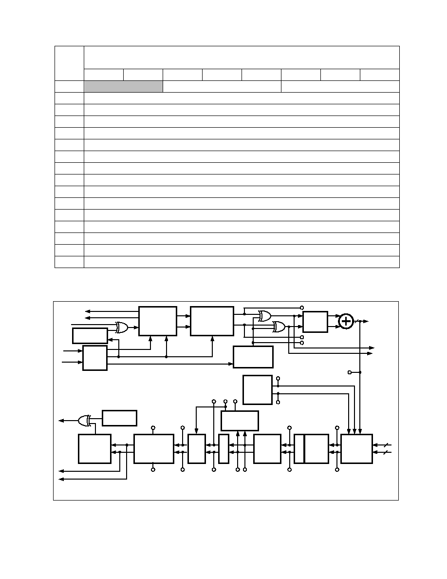
≠≠≠≠≠≠≠≠≠≠≠≠≠≠≠≠≠≠≠≠≠≠≠≠≠≠≠≠≠≠≠≠≠≠≠≠≠≠≠≠≠≠≠≠≠≠≠≠≠≠≠≠
STEL-2000A
20
Bits 3-0
of 38
H
RXTEST
7-0
output
Bit 7
Bit 6
Bit 5
Bit 4
Bit 3
Bit 2
Bit 1
Bit 0
0
H
MFQIN
2-0
Matched Filter Q input
MFIIN
2-0
Matched Filter I input
1
H
•Pk-POWER
9-2
. MF peak magnitude output, unsigned binary (changes once per symbol)
2
H
COS
7-0
. Cosine output of NCO (changes every cycle of RXIFCLK)
3
H
SIN
7-0
. Sine output of NCO (changes every cycle of RXIFCLK)
4
H
DCIOUT
16-9
. Downconverter I channel output (changes at RXIFCLK rate)
5
H
DCQOUT
16-9
. Downconverter Q output (changes at RXIFCLK rate)
6
H
ISUM
9-2
. Matched Filter I output (changes twice per chip)
7
H
QSUM
9-2
. Matched Filter Q output (changes twice per chip)
8
H
POWER
9-2
. MF magnitude output, unsigned binary (changes twice per chip)
9
H
ISUM
7-0
. MF viewport I output (changes twice per chip)
A
H
QSUM
7-0
. MF viewport Q output (changes twice per chip)
B
H
Pk-ISUM
7-0
. MF peak I channel output (changes once per symbol)
C
H
Pk-QSUM
7-0
. MF peak Q channel output (changes once per symbol)
D
H
DOT
16-9
. Dot product (changes once per symbol)
E
H
CROSS
16-9
. Cross product (changes once per symbol)
F
H
TXFBK
7-0
. Loopback test output
Table 3. Receiver test functions
R
X
T
EST
(0
)
(B
I
T
S 2
-
0
)
R
X
T
EST
(0
)
(B
I
T
S 5
-
3
)
TX
CLOCK
GENER-
ATOR
SERIAL
TO DIBIT
CONVERTER
DIFFERENTIAL
ENCODER
TX PN CODE
GENERATORS
NCO
COMPLEX
MULTIPLIER
MATCHED
FILTER
POWER
DETECTOR
VI
EW
PO
R
T
SIN
COS
DIBIT TO
SERIAL
CONVERTER
DIFFERENTIAL
DEMODULATOR
AND CARRIER
DISCRIMINATOR
TXIFCLK
TXIN
TXBITPLS
TXTRKPLS
TXMCHP
RXIIN
7-0
RXQIN
7-0
RXOUT
RXIOUT
RXQOUT
TXTEST(0)
TXTEST(2)
TXTEST(1)
I & D
FILTERS
VI
EW
PO
R
T
R
X
T
EST
(4
)
R
X
T
EST
(5
)
PEAK
HOLD
R
X
T
E
ST
(9
)
R
X
T
EST
(A
)
R
X
T
E
ST
(7
)
R
X
T
EST
(6
)
R
X
T
E
ST
(B
)
R
X
T
E
ST
(C
)
R
X
T
E
ST
(1
)
R
X
T
E
ST
(D
)
R
X
T
E
ST
(E)
R
X
T
EST
(3
)
R
X
T
E
ST
(2
)
R
X
T
EST
(8
)
TX OVERLAY
GENERATOR
RX OVERLAY
GENERATOR
QPSK
MODU-
LATOR
TXIFOUT
7-0
TXIOUT
TXQOUT
RXTEST(F)
Figure 6: Transmitter and Receiver Test Points

≠≠≠≠≠≠≠≠≠≠≠≠≠≠≠≠≠≠≠≠≠≠≠≠≠≠≠≠≠≠≠≠≠≠≠≠≠≠≠≠≠≠≠≠≠≠≠≠≠≠≠≠
21
STEL-2000A
CONTROL REGISTERS
Downconverter Registers
Address 00
H
:
Bit 0 -- Frequency Control Word Load
This bit is used to load a frequency control value into
the NCO, thereby changing its output frequency. The
signal is internally synchronized to RXIFCLK to
avoid intrinsic race or hazard timing conditions.
The loading of the NCO may be performed by
various means. Setting this bit provides a
synchronized internal means to control update of the
NCO. Alternatively, the MFLD pin or the STEL-
2000A’s programmable loop filter timing circuitry
may be used.
The M F L D input and bit 0 of address 00
H
are
logically ORed together so that, when either one is
held low, a rising edge on the other triggers the
frequency load function manually. The rising edge of
this bit is synchronized internally so that, on the
following sixth rising edge of RXIFCLK, the
frequency control word is completely registered into
the NCO accumulator. The frequency load command
must not be repeated until after a delay of six
RXIFCLK
cycles.
Address 01
H
:
Bit 0 -- Manual Sample Clock Enable
This bit selects the source of the internal baseband
sampling clock, which should be at twice the nominal
PN chip rate. The clock reference may be either sup-
plied externally by RXMSMPL or generated inter-
nally from RXIFCLK.
When this bit is set high, the baseband sampling rate
of the receiver is controlled by the external
RXMSMPL
signal. When it is set low, the sampling
clock is generated internally (at a rate determined by
the Sample Rate Control counter and set by bits 5-0 of
address 02
H
) and the RXMSMPL input is ignored.
Bit 1 -- Invert Loop Filter Value
This bit allows the sign of the output signal from the
loop filter to be inverted, thereby negating the value
of the signal. The capability to invert the loop filter
value permits the carrier frequency error component
generated in the demodulator to be either added to or
subtracted from the Frequency Control Word of the
NCO. The correct setting will depend on several fac-
tors, including whether high-side or low-side down-
conversion is used.
When this bit is set low, the loop filter output is
negated before being summed with the Frequency
Control Word of the NCO and is thus subtracted from
the FCW; when this bit is set high, the loop filter out-
put is not negated and is added to the FCW.
Bit 2 -- NCO Accumulator Carry In
This bit is primarily used as an internal test function
and should be set low for normal operation. When
this bit is set high, 1 LSB is added to the NCO accu-
mulator each clock cycle. When it is set low, the NCO
accumulator is not affected.
Bit 3 -- Two's Complement Input
The RXIIN
7-0
and RXQIN
7-0
input signals can be in
either two's complement or offset binary formats.
Since all internal processing in the device operates
with two's complement format signals, it is necessary
to convert the RXIIN
7-0
and RXQIN
7-0
inputs in offset
binary format to two’s complement format by invert-
ing the MSBs.
When this bit is set high, the device expects two's
complement format inputs on RXIIN
7-0
and RXQIN
7-
0
. When it is set low, the device expects offset binary
format on RXIIN
7-0
and RXQIN
7-0
. In two's comple-
ment format, the 8-bit input values range from –128 to
+127 (80
H
to 7F
H
); in offset binary format, the values
range from 0 to +255 (00
H
to FF
H
).
Bits 7-4 -- Integrate and Dump Filter Viewport
Control
The STEL-2000A incorporates viewport (data selector)
circuitry to select any three consecutive bits from the
14-bit output of the Integrate and Dump (I & D) Fil-
ters in the Downconverter block as the 3-bit inputs to
the dual-channel PN Matched Filter. The signal levels
of the Integrate and Dump Filter I and Q outputs
reflect the input signal levels and the number of sam-
ples integrated before the filter contents are
“dumped,” where the number of samples is deter-
mined by the baseband sampling rate (nominally,
twice the PN chip rate) and the I.F. sampling rate
(RXIFCLK). Setting the viewport thus effectively
normalizes the I & D Filter outputs before further
processing. The unsigned value, n, of bits 7-4 of
address 01
H
determines the 3-bit inputs to the PN
Matched Filter as the 14-bit I & D Filter outputs
divided by 2
n
. Equivalently, bits 7-4 control the
viewport of the Integrate and Dump Filter outputs as
shown in Table 5. Note that viewport control affects
both I and Q channels of the Integrate and Dump
Filters.
Bits 7-4
I & D bits output to Matched Filter
0
H
2-0
1
H
3-1

≠≠≠≠≠≠≠≠≠≠≠≠≠≠≠≠≠≠≠≠≠≠≠≠≠≠≠≠≠≠≠≠≠≠≠≠≠≠≠≠≠≠≠≠≠≠≠≠≠≠≠≠
STEL-2000A
22
2
H
4-2
3
H
5-3
.....
....
.....
....
A
H
12-10
B
H
13-11
Table 5. Integrate & Dump Filter Viewport Control
Saturation protection is implemented for those cases
when the Integrate and Dump Filter output signal
level overflows the scaled range selected for the PN
Matched Filter. When the scaled value range is
exceeded, the saturation protection limits the output
word to the maximum or minimum value of the
range according to whether the positive or negative
boundary was exceeded.
Address 02
H
:
Bits 5-0 -- Receiver Baseband Sampling (Dump)
Rate Control
The baseband sampling rate should be set to twice the
nominal PN chip rate of the received signal and must
be less than or equal to half the rate of RXIFCLK.
When bit 0 of address 01
H
is set low, the baseband
sampling clock for the Integrate and Dump Filter and
all subsequent receiver circuitry is referenced to
RXIFCLK
and generated internally. The receiver
baseband sampling rate is then set to the frequency of
RXIFCLK
/(n+1), where n is the value stored in bits 5-
0 and must range from 1 to 63. This feature is useful
in cases where a specific sample rate is required that
is an integer sub-multiple of f
RXIFCLK
. In cases where
a sample rate is required that is not an integer sub-
multiple of f
RXIFCLK
, an external baseband sampling
rate can be provided by the RXMSMPL input.
Addresses 03
H
through 06
H
:
NCO Frequency Control Word
The STEL-2000A’s internal NCO is driven by a fre-
quency control word that is the sum of the frequency
discriminator error value (generated in the demodula-
tor) and the 32-bit frequency control word (FCW)
stored in this location. The four 8-bit registers at
addresses 03
H
to 06
H
are used to store the 32-bit fre-
quency control word as shown in Table 6. The LSB of
each byte is stored in bit 0 of each register.
ADDR
6
ADDR
5
ADDR
4
ADDR
3
Bits 31-24
Bits 23-16
Bits 15-8
Bits 7-0
Table 6. NCO FCW Storage
The NCO frequency is then set by the FCW according
to the following formula:
f
RXIFCLK
x FCW
f
NCO
= ––––––––––––––
2
32
In order to avoid in-band aliasing, f
NCO
must not
exceed 50% of f
RXIFCLK
; normally, the FCW should be
set so that f
NCO
does not exceed ~35% of f
RXIFCLK
.
While this limitation may seem to restrict use of the
NCO, higher I.F. transmit or receive frequencies can
generally be achieved by using aliases resulting from
digital sampling. The signal bandwidth with respect
to f
RXIFCLK
, the modulation type, and the use of Direct
I.F. or Quadrature Sampling Mode also restrict the
choice of NCO frequency, as discussed in Appendix I.
Matched Filter Registers
Despreading of the received signal is accomplished in
the STEL-2000A with a dual (I and Q channel) PN
Matched Filter. Furthermore, the STEL-2000A is
designed for burst signal operation, where each data
burst begins with an Acquisition/Preamble symbol
and is then followed by the actual information data
symbols. Two separate and independent PN codes
can be employed, one for the Acquisition/Preamble
symbol, the other for the information symbols.
Accordingly, the PN Matched Filter is supported by
two PN code registers to independently allow the
programming of two distinct codes up to 64 chips in
length. The PN codes are represented as a sequence
of ternary-valued tap coefficients, each requiring 2
bits of storage according to the mapping shown in
Table 7.
Tap Bits 1,0
Tap Coeff.
X 0
0
0
1
+1
1
1
–1
Table 7. PN Matched Filter Tap Values
As a convention, Tap 0 is the first tap as the received
signal enters the PN Matched Filter, and Tap 63 is the
last. All active taps of the PN Matched Filter, from
Tap 0 up to Tap (N-1), where N is the length of the
PN code, should be programmed with tap coefficient
values of +1 or -1 according to the PN code sequence.
Setting the end coefficients of the PN Matched Filter
registers to zero values permits the effective length of
the filter to be made shorter than 64 taps.
Addresses 07
H
through 16
H
:
Matched Filter Acquisition/Preamble Symbol
Coefficients
Addresses 07
H
to 16
H
contain the 64 2-bit Acquisi-
≠≠≠≠≠≠≠≠≠≠≠≠≠≠≠≠≠≠≠≠≠≠≠≠≠≠≠≠≠≠≠≠≠≠≠≠≠≠≠≠≠≠≠≠≠≠≠≠≠≠≠≠
23
STEL-2000A
tion/Preamble PN code coefficient values. The 128
bits of information are stored in 16 8-bit registers at
addresses 07
H
to 16
H
as shown in Table 8.
Address 16
H
Bits 7,6
Bits 5,4
Bits 3,2
Bits 1,0
Coeff. 63
Coeff. 62
Coeff. 61
Coeff. 60
Address 15
H
Bits 7,6
Bits 5,4
Bits 3,2
Bits 1,0
Coeff. 59
Coeff. 58
Coeff. 57
Coeff. 56
…
…
…
…
…
…
…
…
Address 08
H
Bits 7,6
Bits 5,4
Bits 3,2
Bits 1,0
Coeff. 7
Coeff. 6
Coeff. 5
Coeff. 4
Address 07
H
Bits 7,6
Bits 5,4
Bits 3,2
Bits 1,0
Coeff. 3
Coeff. 2
Coeff. 1
Coeff. 0
Table 8. Acquisition/Preamble Coefficient Storage
Addresses 17
H
through 26
H
:
Matched Filter Data Symbol Coefficients
Addresses 17
H
to 26
H
contain the 64 2-bit Data Sym-
bol PN code coefficient values. The 128 bits of infor-
mation are stored in 16 8-bit registers at addresses 17
H
to 26
H
as shown in Table 9. The contents of addresses
17
H
to 26
H
are independent of and not affected by the
contents of addresses 07
H
to 16
H
.
Address 26
H
Bits 7,6
Bits 5,4
Bits 3,2
Bits 1,0
Coeff. 63
Coeff. 62
Coeff. 61
Coeff. 60
Address 25
H
Bits 7,6
Bits 5,4
Bits 3,2
Bits 1,0
Coeff. 59
Coeff. 58
Coeff. 57
Coeff. 56
…
…
…
…
…
…
…
…
Address 18
H
Bits 7,6
Bits 5,4
Bits 3,2
Bits 1,0
Coeff. 7
Coeff. 6
Coeff. 5
Coeff. 4
Address 17
H
Bits 7,6
Bits 5,4
Bits 3,2
Bits 1,0
Coeff. 3
Coeff. 2
Coeff. 1
Coeff. 0
Table 9. Data Symbol Coefficient Storage
Address 27
H
:
Bit 0 -- Front End Processor Disable
The Front End Processor (FEP) averages the two
baseband samples per chip by adding consecutive
pairs of samples. The function may be disabled for
test purposes by using this bit: when set low, the FEP
is enabled and in its normal mode of operation; when
set high, the FEP is disabled.
Power Estimator Registers
Address 28
H
:
Bits 1-0 -- Matched Filter Viewport Control
The STEL-2000A incorporates viewport (data selector)
circuitry to select any eight consecutive bits from the
10-bit outputs of the PN Matched Filter as the 8-bit
inputs to the Power Estimator and DPSK Demodula-
tor blocks. The Symbol Tracking Processor, however,
operates on the full 10-bit PN Matched Filter outputs
before the viewport is applied. The signal levels of
the PN Matched Filter output reflect the number of
chips per symbol and the signal-to-noise ratio of the
signal. Setting the viewport thus effectively normal-
izes the PN Matched Filter outputs prior to further
processing. The unsigned value, n, of bits 1-0 of
address 28
H
determines the 8-bit input to the Power
Estimator and DPSK Demodulator blocks as the 10-bit
PN Matched Filter output divided by 2
n
. Equiva-
lently, bits 1-0 control the viewport of the PN
Matched Filter output as shown in Table 10. Note
that viewport control affects both I and Q channels of
the PN Matched Filter output.
Bits 1-0
ISUM, QSUM
0
0
Bits 7-0
0
1
Bits 8-1
1
X
Bits 9-2
Table 10. Matched Filter Viewport Control
Saturation protection is implemented for those cases
when the PN Matched Filter output signal level over-

≠≠≠≠≠≠≠≠≠≠≠≠≠≠≠≠≠≠≠≠≠≠≠≠≠≠≠≠≠≠≠≠≠≠≠≠≠≠≠≠≠≠≠≠≠≠≠≠≠≠≠≠
STEL-2000A
24
flows the scaled range selected for the Power Estima-
tor and DPSK Demodulator. When the scaled value
range is exceeded, the saturation protection limits the
output word to the maximum or minimum value of
the range according to whether the positive or nega-
tive boundary was exceeded.
Acquisition and Tracking Processor Registers
The Acquisition and Tracking Processor Registers
allow the user to configure how the PN Matched Fil-
ter outputs for the Acquisition/Preamble symbol and
the data symbols that follow thereafter are treated in
the Symbol Tracking Processor. Since operation of
the STEL-2000A receiver presumes symbol-
synchronous PN modulation, processing of the PN
Matched Filter outputs can be used for symbol
synchronization prior to DPSK demodulation. The
Acquisition/Preamble symbol and the data symbols
may have different PN spreading codes, however,
and so the PN Matched Filter outputs may exhibit
different signal levels due to the different code
lengths and autocorrelation properties. The control
registers in this block allow such differences to be
treated, as well as permitting specification of the
number of receive data symbols per burst and other
parameters associated with burst data
communications.
The I and Q channel outputs of the PN Matched Filter
are processed to estimate the correlation signal power
at each baseband sampling instant. This estimated
signal power is compared with the contents of the
Acquisition/Preamble and Data Symbol Threshold
registers, as appropriate, to determine whether
“successful” correlation has been detected. Successful
detection in acquisition mode immediately switches
the receiver to despread and track the expected sub-
sequent data symbols, while successful detection
thereafter yields symbol synchronization. The thresh-
old register values must be set by the user to satisfac-
torily detect the correlation peak in noise obtained
when the received PN-spread signal is correlated
against a local version of the PN code by the PN
Matched Filter. Once the power estimation value
exceeds the threshold register value, a successful cor-
relation is assumed to have been detected. Further
operations in the Symbol Tracking Processor then
handle the possibility of multiple detects per symbol,
missed detects, etc.
The choice of the threshold values will be determined
by several factors. Arithmetically, the digital base-
band samples of the received signal are multiplied by
the PN Matched Filter tap coefficients each baseband
sample clock cycle and the results are summed to
provide a correlation value. The I and Q PN Matched
Filter correlated output values are then used to esti-
mate the signal power according to the following
approximation:
Max{Abs(I),Abs(Q)}+
1
/
2
Min{Abs(I), Abs(Q)}.
The magnitude of the estimated power thus depends
on several variables, including the setting of the Inte-
grate and Dump Filter viewport, the PN code length
and autocorrelation properties, and the magnitudes of
the incoming RXIIN
7-0
and RXQIN
7-0
signals. The
actual threshold values that should be programmed
will therefore vary from application to application.
Addresses 29
H
and 2A
H
:
Acquisition/Preamble Threshold
Addresses 29
H
and 2A
H
contain the unsigned Acqui-
sition/Preamble Threshold value, as shown in Table
11. This value is used for comparison with the esti-
mated signal power from the PN Matched Filter to
determine whether a successful correlation has been
detected in acquisition mode. The Acquisi-
tion/Preamble Threshold value must be set by the
user to satisfactorily detect the correlation peak in
noise obtained when the received PN-spread Acquisi-
tion/Preamble is correlated against a local version of
the Acquisition/Preamble PN code by the PN
Matched Filter. Once the power estimation value
exceeds the threshold value, a successful correlation is
assumed to have been detected. Note that the Symbol
Tracking Processor does not insert missed detect
pulses when the device is in acquisition mode.
ADDR 2A
H
ADDR 29
H
Bits 1-0
Bits 7-0
Acq. Thresh. Bits 9-8
Acq. Thresh. Bits 7-0
Table 11. Acquisition/Preamble Threshold Storage
Addresses 2B
H
and 2C
H
:
Data Symbol Threshold
Addresses 2B
H
and 2C
H
contain the Data Symbol
Threshold value, as shown in Table 12. This value is
used for comparison with the estimated signal power
from the PN Matched Filter to determine whether a
successful correlation has been detected for each data
symbol. The Data Symbol Threshold value must be
set by the user to satisfactorily detect the correlation
peak in noise obtained when the received PN-spread
data symbol is correlated against a local version of the
data symbol PN code by the PN Matched Filter. Once
the power estimation value exceeds the threshold
value, a successful correlation is assumed to have
been detected. If bit 2 of address 30
H
is set low, then
the Symbol Acquisition Processor will insert a detect
pulse at the appropriate time if a successful correla-
tion is not detected as expected a priori.

≠≠≠≠≠≠≠≠≠≠≠≠≠≠≠≠≠≠≠≠≠≠≠≠≠≠≠≠≠≠≠≠≠≠≠≠≠≠≠≠≠≠≠≠≠≠≠≠≠≠≠≠
25
STEL-2000A
Table 12. Data Symbol Threshold Storage
Address 2D
H
:
Bits 5-0 -- Rx Chips per Data Symbol
The number of PN chips per data symbol in the
receiver is controlled by address 2D
H
. The unsigned
value must range from 1 to 63 (01
H
to 3F
H
), where the
number of chips per data symbol will be this value
plus 1. The a priori number of PN chips per data sym-
bol, where this value must be equal to the number of
non-zero coefficients stored in the Data Symbol Coef-
ficient Registers (addresses 17
H
to 26
H
) for the PN
Matched Filter, is used to help control symbol timing
in the receiver. Since acquisition is purely based on
correlation of a single received Acquisition/Preamble
symbol, the corresponding number of chips per
Acquisition/Preamble symbol is not required and no
similar register is provided for such use.
Address 2E
H
:
Receiver Data Symbols per Burst (bits 7-0)
The data stored as two bytes in addresses 2E
H
(LS
Byte) and 3A
H
(MS Byte) defines the number of data
symbols per burst. This unsigned value must range
from 3 to 65,535 (0003
H
to FFFF
H
), and the number of
data symbols per burst will be this value minus 2,
giving a range of 1 to 65,533. Note that the range is
slightly different from that supported by the STEL-
2000A’s transmitter. Once the number of received
data symbols processed exceeds this number, the
burst is assumed to have ended and the receiver
immediately returns to acquisition mode, ready for
the next burst.
Address 2F
H
:
Missed Detects per Burst Threshold
To monitor the reception quality of the received burst
data symbols, the STEL-2000A incorporates a feature
within its tracking algorithm that tallies the number
of received data symbols whose PN Matched Filter
correlation output did not exceed the Data Symbol
Threshold value.
Whenever a "missed detect" occurs, the tracking algo-
rithm will generate and insert a detect signal at the
sample clock cycle corresponding to the expected cor-
relation peak in order to maintain a continuous train
of data symbols and symbol clocks. Simultaneously,
a "missed detect" pulse will be generated internally
and tallied for the current burst. When the
accumulated number of missed detects is greater than
the value stored in address 2F
H
, the device will
terminate reception of the current burst and return to
acquisition mode to await the next burst.
The unsigned value in address 2F
H
must range from 1
to 255 (01
H
to FF
H
), where this value is the maximum
number of missed detects per burst allowed before
the burst terminates. This function can be disabled by
setting bit 5 of address 30
H
high.
Address 30
H
:
Bit 0 -- Manual Detect Enable
While the receiver is in acquisition mode, valid bursts
may be ignored by setting this bit high. When it is set
low (normal operation), the detection of a burst's
Acquisition/Preamble symbol is enabled. Setting this
bit high allows the user to force the device to ignore
Acquisition/Preamble symbols that would normally
be successfully acquired. This feature could be used,
for example, in a system employing multiple receivers
with identical PN codes in a Time Division Multiple
Access scheme where time-synchronized device man-
agement could be supported through dynamic setting
of this bit.
Bit 1 -- Manual Punctual
This bit enables the user to completely disable the
internal tracking circuitry and force symbol informa-
tion to be transferred to the demodulator punctually
at the symbol rate determined by the number of chips
per data symbol information programmed into
address 2D
H
. This function overrides the symbol
tracking algorithm, although the absence of a success-
ful correlation will continue to be tallied as a missed
detect and compared against the value stored in
address 2F
H
to monitor signal quality unless disabled
by bit 5 of address 30
H
. When bit 1 is set low, the
STEL-2000A will operate in its normal mode with
symbol timing derived from the symbol tracking pro-
cessor; when set high, symbol timing is derived from
the a priori number of chips per data symbol stored in
bits 5-0 of address 2D
H
.
Bit 2 -- Force Continuous Acquisition
This bit enables the user to force the receiver to
remain in acquisition mode even after successful
detection of the Acquisition/Preamble symbol. When
so commanded, the receiver will continuously process
only Acquisition/Preamble symbols and will not
switch from acquisition mode. This function may be
used under manual control to receive a series of
repeated Acquisition/Preamble symbols in order to
increase the confidence level of burst detection before
beginning demodulation of the data symbol informa-
tion.
ADDR 2C
H
ADDR 2B
H
Bits 1-0
Bits 7-0
Data Thresh. Bits 9-8
Data Thresh. Bits 7-0

≠≠≠≠≠≠≠≠≠≠≠≠≠≠≠≠≠≠≠≠≠≠≠≠≠≠≠≠≠≠≠≠≠≠≠≠≠≠≠≠≠≠≠≠≠≠≠≠≠≠≠≠
STEL-2000A
26
When this bit is set high, the device will be locked in
acquisition mode and the Symbol Tracking Processor
will not insert missed detect pulses; when set low,
normal operation will be enabled whereby data sym-
bols are automatically processed immediately follow-
ing detection of an Acquisition/Preamble symbol.
Bit 3 -- Bypass Max. Power Selector
The STEL-2000A’s receiver acquisition and tracking
circuitry includes a function that continuously selects
the highest estimated power level out of the three
most recent consecutive estimated power levels from
the PN Matched Filter. As the contents of the sliding
3-sample window change each cycle of the baseband
sampling clock, a new determination of the highest
power level is made from the current set of the three
most recent power level values. The correlated I and
Q channel values within the 3-sample window corre-
sponding in time to the highest observed power level
are then available to be processed in the demodulator.
This function assures that, within any 3-sample
period, the I and Q channel values corresponding to
the highest estimated power level will be selected
over the two other pairs of correlated values even if
the estimated power levels of the other pairs exceed
the programmed threshold. The Maximum Power
Selector is used in normal operation of the STEL-
2000A so that the tracking algorithm discriminates by
estimated power levels rather than exact timing inter-
vals, thereby allowing the receiver to adjust to dyna-
mic changes of the symbol phase. In cases where spe-
cific correlation values are desired regardless of their
associated power level, bit 3 of address 30
H
enables
the 3-sample power discriminator to be bypassed,
thereby making the outputs of the PN Matched Filter
available directly to the demodulator.
When this bit is set high, the Maximum Power Selec-
tor is bypassed; when it is set low, the Selector is
enabled, where this is the normal operating mode.
Bit 4 -- Half Symbol Pulse Off
The STEL-2000A generates two bit clock pulses per
symbol when operating in QPSK mode, one at the
mid-point of each symbol and one at the end of each
symbol. These clocks are used by the Output Proces-
sor to manage data flow.
When this bit is set high, the mid-point pulse is sup-
pressed; when it is set low, the device operates in its
normal mode. This function is primarily used for test
purposes and should not normally be used.
Bit 5 -- Missed Detects Per Burst Off
To monitor the quality of the received burst data
symbols, the Symbol Tracking Processor keeps track
of the cumulative number of received data symbols
per burst whose estimated correlation power level did
not exceed the specified Data Symbol Threshold
value. When the accumulated number of missed
detects equals the Missed Detects per Burst Threshold
value stored in address 2F
H
, the device will terminate
the reception of the current burst with the next
missed detect and return to acquisition mode to await
the next burst.
When bit 5 is set low, the "missed detect" function
operates normally; when set high, this function is dis-
abled, allowing the device to be operated until the
end of the specified data burst even when the number
of “missed detects” exceeds the Missed Detects per
Burst Threshold.
Bit 6 -- Receiver Symbols Per Burst Off
The data stored in addresses 2E
H
and 3A
H
defines the
number of data symbols per burst that will be pro-
cessed by the receiver. This unsigned value must
range from 3 to 65,535 (0003
H
to FFFF
H
), and the
number of data symbols per burst will be this value
minus 2. Once the number of data symbols processed
by the receiver exceeds this number, the burst is
assumed to have ended and the receiver will immedi-
ately return to acquisition mode.
When bit 6 is set high, the function is disabled, pro-
viding an option to track data symbols under external
control for bursts of more than 65,533 data symbols or
indefinitely for continuous transmission; when set
low, the function will operate normally as defined by
the value stored in addresses 2E
H
and 3A
H
.
Address 31
H
:
Bit 0 -- Manual Detect Pulse
This bit provides the user a means to externally gen-
erate symbol timing, bypassing and overriding the
internal symbol power estimation and tracking cir-
cuitry. This function may be useful in applications
where the dynamic characteristics of the transmission
environment require unusual adjustments to the
symbol timing.
When bit 0 of address 30
H
is set high (Manual Detect
Enable) and when RXMDET is low, a rising edge on
this bit will generate a detect pulse. The function can
also be performed by means of the RXMDET input
signal. Bit 0 of address 31
H
and the RXMDET input
are logically ORed together so that, when either one is
held low, a rising edge on the other triggers the man-
ual detect function. The rising edge of this bit is syn-
chronized internally so that on the second rising edge
≠≠≠≠≠≠≠≠≠≠≠≠≠≠≠≠≠≠≠≠≠≠≠≠≠≠≠≠≠≠≠≠≠≠≠≠≠≠≠≠≠≠≠≠≠≠≠≠≠≠≠≠
27
STEL-2000A
of the baseband sampling clock that follows, the
rising edge of bit 0 will transfer the I and Q channel
correlated output values of the PN Matched Filter to
the DPSK Demodulator.
Address 32
H
:
Bit 0 -- Receiver Manual Abort
This bit enables the user to manually force the STEL-
2000A to cease reception of the present burst of data
symbols and prepare for acquisition of a new burst.
This function can be used to reset the receiver and
prepare to receive a priority transmission signal
under precise timing control, giving the user the abil-
ity to control the current state of the receiver as
needed.
When RXMABRT is set low, a rising edge on bit 0 of
address 32
H
will execute the abort function. The
function can also be performed by means of the
RXMABRT
input. The RXMABRT input and bit 0 of
address 32
H
are logically ORed together so that, when
either one is held low, a rising edge on the other trig-
gers the abort function. The second rising edge of the
internal baseband sampling clock that follows a rising
edge of this bit will execute the abort and also clear
the symbols-per-burst, samples-per-symbol, and
missed-detects-per-burst counters. The counters will
be reactivated on the detection of the next Acquisi-
tion/Preamble symbol or by a manual detect signal.
Demodulator Registers
Address 33
H
:
Bits 1-0 -- Signal Rotation Control
These bits control the function of the Signal Rotation
Block used in demodulation of the differentially
encoded BPSK, QPSK, or
/4 QPSK signals. The
previous symbol will be rotated in phase with respect
to the current symbol as shown in Table 13, where I
out
and Q
out
are the I and Q channel outputs of the Signal
Rotation Block and I
in
and Q
in
are the inputs. The
normal settings are 0 X (no rotation) for BPSK and
/4 QPSK signals and 1 1 (–45
∞
rotation) for
conventional QPSK signals.
Bits 1,0
I
out
Q
out
Resulting Rotation
0 X
I
in
Q
in
No rotation
1 0
I
in
– Q
in
Q
in
+ I
in
+45
∞
rotation
1 1
I
in
+ Q
in
Q
in
– I
in
–45
∞
rotation
Table 13. Signal Rotation Control
Bit 2 -- Not used
Bit 2 of address 33
H
is not used and should always be
set low.
Bit 3 -- Loop Clear Disable
The setting of this bit determines whether the Loop
Filter's K2 accumulator is reset or not when the STEL-
2000A receiver function is turned off when the input
signal MRXEN is set low.
When bit 3 is set low, the Loop Filter's K2 accumula-
tor will be reset to zero whenever MRXEN is set low
to disable the receiver function. When bit 3 is set
high, this function is disabled and the contents of the
accumulator are not affected when MRXEN transi-
tions from high to low. The optimum setting of this
bit will depend on the stability of the oscillators used
for carrier generation and frequency translation in the
system and the length of the period between bursts.
If the oscillators are stable and the period between
bursts is not very long, the optimum setting of this bit
will be low so that at the start of each burst the track-
ing loop will resume from its state at the end of the
previous burst. If the oscillators are not stable or if
the period between bursts is long with respect to the
oscillators’ stability, then the optimum setting may be
high so that the tracking loop will restart from its ini-
tial state at the start of each burst.
Bits 7-4 -- AFC Viewport Control
The STEL-2000A incorporates viewport (data selector)
circuitry to select any eight consecutive bits from the
17-bit output of the Frequency Discriminator as the
8-bit input to the Loop Filter block to implement the
STEL-2000A’s AFC function. The unsigned value, n,
of bits 7-4 of address 33
H
determines the 8-bit input to
the Loop Filter as the 17-bit Frequency Discriminator
output divided by 2
n
. Equivalently, bits 7-4 control
the viewport of the Frequency Discriminator output
as shown in Table 14.
Bits 7-4
Discrim. bits output to Loop Filter
0
H
7-0
1
H
8-1
2
H
9-2
3
H
10-3
…
…
…
…
8
H
15-8
9
H
16-9
A
H
- F
H
not used
Table 14. AFC Viewport Control
Saturation protection is implemented for those cases
when the Frequency Discriminator output signal level

≠≠≠≠≠≠≠≠≠≠≠≠≠≠≠≠≠≠≠≠≠≠≠≠≠≠≠≠≠≠≠≠≠≠≠≠≠≠≠≠≠≠≠≠≠≠≠≠≠≠≠≠
STEL-2000A
28
overflows the scaled range selected for the Loop Fil-
ter. When the scaled value range is exceeded, the sat-
uration protection limits the output word to the max-
imum or minimum value of the range according to
whether the positive or negative boundary was
exceeded.
Address 34
H
:
Bits 4-0 -- K2 Gain Value
Bits 4-0 control the gain factor K2 within the Loop Fil-
ter. The gain factor multiplies the signal before the
K2 accumulator by a value of 2
n
, where n is the 5-bit
K2 Gain Value. The value must range from 0 to 21
(15
H
) as shown in Table 15.
Bits 4-0
Gain in K2 Path
00
H
2
0
01
H
2
1
.....
....
.....
....
14
H
2
20
15
H
2
21
Table 15. K2 Gain Values
Bit 5 -- K2 On
This bit enables or disables the K2 path of the Loop
Filter. Setting this bit low resets the K2 accumulator
and keeps it reset; setting this bit high enables the
path and turns on K2.
Bit 6 -- Carry In One Half
When this bit is set high, the value of
1
/
2
of an LSB is
added to the accumulator of the K2 path of the Loop
Filter each symbol period. This function can be useful
in cases where the scale and gain functions that pre-
cede the accumulator produce quantized values with
significant error. In such cases, the processing of
two's complement numbers by the accumulator will
compound the error over time. Since truncation of
two's complement numbers leads to a negative bias of
1
/
2
of an LSB when the error is random, adding
1
/
2
of
an LSB per symbol can compensate by averaging the
error to zero.
When bit 6 of address 34
H
is set high, a value of
1
/
2
will be added to the accumulator input each symbol
cycle; when it is low, a zero will be added.
Address 35
H
:
Bits 4-0 -- K1 Gain Value
Bits 4-0 control the gain factor K1 within the Loop Fil-
ter. The gain factor multiplies the signal by a value of
2
n
, where n is the 5-bit K1 Gain Value. The value
must range from 0 to 21 (15
H
), as shown in Table 16.
Bits 4-0
Gain in K1 Path
00
H
2
0
01
H
2
1
.....
....
.....
....
14
H
2
20
15
H
2
21
Table 16. K1 Gain Values
Bit 5 -- K1 On
This bit enables or disables the K1 path of the Loop
Filter. Setting this bit low disables the K1 path; set-
ting this bit high enables the path and turns on K1.
Bit 6 -- Freeze Loop
This bit enables the Loop Filter to be held constant
during symbol cycles, thereby fixing the output fre-
quency of the NCO at the value established by the
Loop Filter when bit 6 was set high. This function can
be useful in cases where a carrier offset has been
tracked by the Loop Filter and additional Doppler off-
sets are to be ignored.
When this bit is set high, it freezes the output of the
Loop Filter; when it is set low, the Loop Filter is
enabled and processes the frequency error informa-
tion in the usual way.
Output Processor Control Registers
Address 36
H
:
Bit 0 -- Reverse I and Q
In QPSK mode, the order in which the received I and
Q bit information is output may be reversed by set-
ting this bit high. This function has the effect of inter-
changing I and Q channels. Normally, when this bit
is set low, the I-channel bit will precede the Q-channel
bit in each symbol period. When bit 0 is set high, the
Q-channel bit will precede the I-channel bit each sym-
bol period.
Bit 1 -- BPSK Enable
This bit configures the Output Processor to output
either one bit per symbol (BPSK mode) or two bits per
symbol (QPSK mode). In addition, it enables the user
to output the I-channel information only or the Q-
channel information only, depending on the value of
bit 0. Table 17 shows the configuration of the output
processor for all combinations of the values of bits 0
and 1.
Bit 1
Bit 0
Output Processor Mode
0
0
QPSK mode with I-Channel Bit
Preceding Q-Channel Bit

≠≠≠≠≠≠≠≠≠≠≠≠≠≠≠≠≠≠≠≠≠≠≠≠≠≠≠≠≠≠≠≠≠≠≠≠≠≠≠≠≠≠≠≠≠≠≠≠≠≠≠≠
29
STEL-2000A
0
1
QPSK mode with Q-Channel Bit
Preceding I-Channel Bit
1
0
BPSK mode with I-Channel
Information Output
1
1
BPSK mode with Q-Channel
Information Output
Table 17. Output Processor Modes
Bit 1 also sets the Frequency Discriminator into either
BPSK or QPSK mode. The STEL-2000A receiver uses
dot and cross product results generated within the
DPSK Demodulator to develop the error signal used
to form a closed-loop AFC for carrier frequency
acquisition and tracking.
When bit 1 is set high, the discriminator circuitry is in
BPSK mode and the Frequency Discriminator func-
tion is calculated as:
Cross
16-0
x Dot
MSB
.
When bit 1 is set low, the discriminator circuitry is in
QPSK mode and the Frequency Discriminator func-
tion is calculated as:
(Cross
16-0
x
Dot
MSB
)
–
(Dot
16-0
x
Cross
MSB
).
Bit 2 -- Invert Output
This bit inverts the output bits of both the I and Q
Channels. The inversion will occur at the output pins
RXOUT
, RXIOUT, and RXQOUT.
When this bit is set low, the outputs are not inverted;
when it is set high, the outputs are inverted.
Address 37
H
:
Bit 0 -- NCO Enable
The function of this bit is to allow the power con-
sumed by the operation of the NCO circuitry to be
minimized when the STEL-2000A is not receiving.
The NCO can also be disabled while the STEL-2000A
is transmitting provided that the STEL-2000A’s on-
chip BPSK/QPSK modulator is not being used. With
the instantaneous acquisition properties of the PN
Matched Filter, it is often desirable to shut down the
receiver circuitry to reduce power consumption,
resuming reception periodically until an Acquisi-
tion/Preamble symbol is acquired. Setting bit 0 low
will do this by holding the NCO in a reset state. After
this bit has been set high again to re-activate the NCO
it will be necessary to reload the frequency control
word into the NCO. Note that this bit operates inde-
pendently of bits 1 (Transmitter Enable) and 2
(Receiver Enable)
, which have similar control over
the transmit and receive circuits, respectively.
Bit 0 of address 37
H
performs the same function as
MNCOEN
, and these two signals are logically ORed
together to form the overall control function. When
this bit is set low, MNCOEN controls the activity of
the NCO circuitry and, when MNCOEN is set low, bit
0 controls the activity of the NCO circuitry. When
either bit 0 or MNCOEN (whichever is in control, as
defined above) goes low, a reset sequence occurs on
the following RXIFCLK cycle to virtually disable all
of the NCO circuitry, although the user pro-
grammable control registers are not affected by the
power down sequence. Upon reactivation (when
either MNCOEN or bit 0 of address 37
H
return high),
the NCO must be reloaded with frequency control
information either by means of the MFLD input or by
writing 01
H
into address 00
H
.
Bit 1 -- Transmitter Enable
A rising edge on this bit causes the transmit sequence
to begin so that the STEL-2000A first transmits a sin-
gle Acquisition/Preamble symbol followed by data
symbols. Bit 1 of address 37
H
should be set low after
the last symbol has been transmitted to minimize
power consumption of the transmitter circuit. Bit 1 of
address 37
H
operates independently of bits 2 and 0,
where those bits have similar control over the receive
and NCO circuitry, respectively.
When input signal MTXEN is set low, bit 1 of address
37
H
controls the activity of the transmit circuitry and,
when MTXEN is set low, bit 1 controls this function.
When either bit 1 or MTXEN (whichever is in control,
as defined above) goes low, a reset sequence occurs
on the following TXIFCLK cycle to virtually disable
all of the transmitter data path, although the user
programmable control registers are not affected by
the power down sequence.
Bit 2 -- Receiver Enable
The function of this bit is to allow power consumed
by the operation of the receiver circuitry to be mini-
mized when the device is not receiving. With the
instantaneous acquisition properties of the PN
Matched Filter, it is often desirable to shut down the
receiver circuitry to reduce power consumption,
resuming reception periodically until an Acquisi-
tion/Preamble symbol is acquired. Setting bit 2 low
reduces the power consumption substantially. When
bit 2 is set high, the receiver will automatically power
up in acquisition mode regardless of its prior state
when it was powered down. Bit 2 of address 37
H
operates independently of bits 1 and 0 of address
37
H
,where these signals have similar control over the
transmit and NCO circuitry, respectively.
Bit 2 of address 37
H
performs the same function as
MRXEN
, and these two signals are logically ORed
together to form the overall control function. When
bit 2 of address 37
H
is set low, MRXEN controls the
activity of the receiver circuitry and, when MRXEN is
set low, bit 2 of address 37
H
controls the activity of
the receiver circuitry. When either bit 2 or MRXEN
≠≠≠≠≠≠≠≠≠≠≠≠≠≠≠≠≠≠≠≠≠≠≠≠≠≠≠≠≠≠≠≠≠≠≠≠≠≠≠≠≠≠≠≠≠≠≠≠≠≠≠≠
STEL-2000A
30
(whichever is in control, as defined above) goes low, a
reset sequence begins on the following RXIFCLK
cycle and continues through a total of six RXIFCLK
cycles to virtually disable all of the receiver data
paths, although the user programmable control regis-
ters are not affected by the power down sequence.
Note that this reset sequence will also reset the con-
tents of address 38
H
to 0. If the R X T E S T
7-0
bus is
being used for reading any function except the
Matched Filter I and Q inputs the value required must
be re-written after re-enabling the receiver.
Address 38
H
:
Bits 3-0 -- RXTEST
7-0
Function Select
The data stored in bits 3-0 of address 38
H
selects the
signal available at the RXTEST
7-0
bus (pins 41-48).
These pins provide access to 16 test points within the
receiver according to the data stored in bits 3-0 of
address 38
H
and the assignments shown in Table 3.
Note that the validity of the RXTEST
7-0
bus signals at
RXIFCLK frequencies over 20 MHz is dependent on
the function selected. Functions that change more
rapidly than once per symbol may be indeterminate
at clock frequencies higher than 20 MHz. Note that
the reset sequence that occurs whenever the receiver
is disabled will also reset the contents of address 38
H
to 0. If the RXTEST
7-0
bus is being used for reading
any function except the Matched Filter I and Q inputs
the value required must be re-written after disabling
the receiver.
Address 39
H
:
Bits 6-0 -- Matched Filter Power Saver
The data stored in bits 6-0 of address 39
H
allows the
unused sections of the PN Matched Filter to be turned
off when the PN Matched Filter is configured to be
less than 64 taps long for data symbols. All taps are
always fully powered when the device is in
acquisition mode.
The PN Matched Filter is split into seven 9-tap sec-
tions, and the power to each section is controlled by
the settings of bits 6-0 of address 39
H
, as shown in
Table 18.
Bit in Addr. 39
H
MF Taps Controlled
0
1-9
1
10-18
2
19-27
3
28-36
4
37-45
5
46-54
6
55-63
Table 18. Matched filter tap power control
Power control is not provided for Tap 0, the first tap
of the PN Matched Filter, since Tap 0 is always used
no matter what the PN code length. Setting a bit high
in bits 6-0 of address 39
H
turns off the power to the
corresponding block of taps of the PN Matched Filter.
The power should only be turned off to those blocks
of taps for which all the tap coefficients in that block
have been set to zero
Address 3A
H
:
Receiver Data Symbols per Burst (bits 15-8)
The data stored as two bytes in addresses 2E
H
(LS
byte) and 3A
H
(MS byte) defines the number of data
symbols per burst. This unsigned value must range
from 3 to 65,535 (0003
H
to FFFF
H
), and the number of
data symbols per burst will be this value minus 2,
giving a range of 1 to 65,533. Note that the range is
slightly different from that in the transmitter. Once
the number of received data symbols processed
exceeds this number, the burst is assumed to have
ended and the STEL-2000A immediately returns to
acquisition mode to await the next burst.
Address 3B
H
:
Bit 0 -- Matched Filter Loopback Enable
The STEL-2000A incorporates a loopback capability
that feeds the encoded and spread transmit signals
TXIOUT
and TXQOUT directly into the PN Matched
Filter inputs. This test mode allows the baseband
portion of the system to be tested independently of
the BPSK/QPSK Modulator and Downconverter.
Setting bit 0 of address 3B
H
high enables this loop-
back path; setting it low puts the device into its nor-
mal operating mode.
Bit 1 -- I.F. Loopback Enable
The STEL-2000A incorporates a loopback capability
that feeds the encoded, spread and modulated trans-
mit signal TXIFOUT
7-0
directly into the receiver
RXIIN
7-0
input. This test mode allows the entire digi-
tal portion of the system to be tested. Since only the I
channel is provided as an input, I.F. loopback requires
that the PN chip rate and RXIFCLK rate be consistent
with Direct I.F. Sampling Mode.
Setting bit 1 of address 3B
H
high enables this loop-
back path; setting it low puts the device into its
normal operating mode.
Bits 3-2 -- Receiver Overlay Select
The STEL-2000A incorporates programmable overlay
code generators in both the transmitter and receiver.
When enabled, the selected receiver overlay code is
subtracted from the data symbols, one overlay bit per
symbol in both BPSK and QPSK modes. No synchro-
nization beyond the burst acquisition synchronization
that is intrinsic to operation of the STEL-2000A is

≠≠≠≠≠≠≠≠≠≠≠≠≠≠≠≠≠≠≠≠≠≠≠≠≠≠≠≠≠≠≠≠≠≠≠≠≠≠≠≠≠≠≠≠≠≠≠≠≠≠≠≠
31
STEL-2000A
required since the overlay code generators in both the
transmitter and the receiver are automatically reset at
the start of each burst. The addition of the overlay
code randomizes the transmitted data sequence to
guarantee that the spectrum of the transmitted signal
will be adequately whitened and will not contain a
small number of spectral lines even when the data
itself is not random.
Three transmit and receive overlay codes can be
selected, where they are each maximal length
sequences with lengths of 63, 511 and 1023 symbols.
The receiver overlay codes are enabled and selected
by the settings of bits 3-2 of address 3B
H
, as shown in
Table 19.
Bits 3-2 in
Addr. 3B
H
Overlay Code length
and polynomial
0
Overlay code disabled
1
63: 1 + x
2
+ x
3
+ x
5
+ x
6
2
511: 1 + x
2
+ x
3
+ x
5
+ x
9
3
1023: 1 + x
2
+ x
3
+ x
5
+ x
10
Table 19. Receiver Overlay Code Select
Addresses 3C
H
to 3F
H
are unused.
Transmit Control Registers
Address 40
H
:
Bit 0 -- Transmit BPSK
This bit configures the transmitter for either BPSK or
QPSK mode transmission. and differential encoding.
If programmed for BPSK mode, data is requested by
the STEL-2000A by a rising edge of output signal
TXBITPLS
, where TXBITPLS is generated once per
symbol, one chip period before the end of the current
symbol. At the end of the symbol duration, the TXIN
data is latched into the device. TXBITPLS falls low
immediately following the rising edge of TXIFCLK,
which latches the TXIN value, and is generated
repeatedly at the symbol rate as long as the input sig-
nal MTXEN remains high.
In QPSK mode, data is requested by the STEL-2000A
by a rising edge of output signal TXBITPLS, where
this signal is generated in this mode twice per
symbol, first one chip period before the middle of the
symbol and then one chip period before the end of the
symbol. TXBITPLS requests the data exactly one
chip cycle before latching the TXIN data into the
device. TXBITPLS falls low immediately following
the rising edge of TXIFCLK, which latches the TXIN
value.
When bit 0 of address 40
H
is set low, the transmitter is
configured in QPSK mode; when it is set high, the
transmitter is configured in BPSK mode.
Bit 1 -- Offset Binary Output
The TXIFOUT
7-0
output signals can be in either two's
complement or offset binary formats. Since all inter-
nal processing in the device uses two's complement
format signals, the MSB of the two’s complement
modulated transmitter output must be inverted if the
output is to be in offset binary format.
When this bit is set high, the TXIFOUT
7-0
output will
be in offset binary format and, when it is set low, the
signal will be in two’s complement format. In two's
complement format, the 8-bit output values range
from –128 to +127 (80
H
to 7F
H
); in offset binary for-
mat, the values range from 0 to +255 (00
H
to FF
H
).
Bit 2 -- Manual Chip Clock Enable
This bit enables the PN chip rate to be controlled by
either the internal chip rate clock generator or by the
external input signal TXMCHP. The TXMCHP input
allows the user to manually insert a single PN chip
clock pulse or continuous stream of pulses. This fea-
ture is useful in cases where a specific chip rate is
required that cannot be derived by the internal clock
generator which generates clocks of integer sub-mul-
tiples of the frequency of TXIFCLK. The signal is
internally synchronized to TXIFCLK to avoid race or
hazard timing conditions.
When this bit is set high, TXMCHP will provide the
PN chip rate clock; when it is set low, the clock will be
provided by the internal chip rate clock generator
controlled by bits 5-0 of address 41
H
.
Bit 3 -- Invert Symbol
This bit allows the user to invert the I and Q channel
bits following differential encoding and before being
spread by the PN code. This function has the same
effect as inverting the PN code, which may be useful
in some cases.
When this bit is set high, the encoded I and Q channel
bits will be inverted; when it is set low, the I and Q
channel bits will not be inverted.
Address 41
H
:
Bits 5-0 -- TXIFCLK Cycles per Chip
Bits 5-0 set the transmitter baseband PN chip rate to
the frequency of TXIFCLK/(n+1), where n is the
value stored in bits 5-0. The value of the data stored
in bits 5-0 must range from 1 to 63 (01
H
to 3F
H
). This
feature is useful when the PN chip rate required is an
integer sub-multiple of the frequency of TXIFCLK. In
cases where a chip rate is required that is not an inte-
ger sub-multiple of the frequency of TXIFCLK, the
rate may be controlled externally using TXMCHP.
Address 42
H
:
≠≠≠≠≠≠≠≠≠≠≠≠≠≠≠≠≠≠≠≠≠≠≠≠≠≠≠≠≠≠≠≠≠≠≠≠≠≠≠≠≠≠≠≠≠≠≠≠≠≠≠≠
STEL-2000A
32
Bits 5-0 -- Tx Chips per Data Symbol
The number of chips per data symbol in the transmit-
ter is stored in bits 5-0 of address 42
H
. The unsigned
value must range from 1 to 63 (01
H
to 3F
H
), and the
number of chips per data symbol will be this value
plus 1. This value controls data symbol timing in the
transmitter.
Address 43
H
:
Bits 5-0 -- Tx Chips per Acquisition/Preamble
Symbol
The number of chips per Acquisition/Preamble sym-
bol in the transmitter is stored in bits 5-0 of address
43
H
. The unsigned value must range from 1 to 63
(01
H
to 3F
H
), and the number of chips per data sym-
bol will be this value plus 1. This value controls the
Acquisition/Preamble symbol timing in the
transmitter.
Addresses 44
H
through 4B
H
:
Transmitter Acquisition/Preamble Symbol Code
Each STEL-2000A burst transmission begins with an
Acquisition/Preamble symbol and is then followed
by the actual information data symbols. Two separate
and independent PN codes can be employed, one for
the Acquisition/Preamble symbol, the other for the
information symbols. Accordingly, the STEL-2000A
Transmit PN Code Generators, like the receiver’s PN
Matched Filter, support independent PN codes up to
64 chips in length for the two modes. Addresses 44
H
to 4B
H
contain the binary Transmitter Acquisi-
tion/Preamble Symbol PN code chip values, where
the configuration of the stored bits is as shown in
Table 20.
Addr 4B
H
, Bits 7-0
Code bits 63-56
.............
.............
Addr 45
H
, Bits 7-0
Code bits 15-8
Addr 44
H
, Bits 7-0
Code bits 7-0
Table 20. Acquisition/Preamble Symbol Codes
The length, N, of the Acquisition/Preamble symbol
code is set by the value of (N-1) stored in bits 5-0 of
address 43
H
. An internal counter begins the transmis-
sion with the PN code chip corresponding to that
value. The last chip transmitted per symbol is then
code chip 0. Note that this convention agrees with
that used for the STEL-2000A’s PN Matched Filter:
for a code of length N, code chip (N-1) will be the first
chip transmitted and will first be processed by Tap 0
of the PN Matched Filter; the last chip per symbol to
be transmitted, however, will be chip 0, and at that
time chip (N-1) will be processed by Tap (N-1) and
chip 0 by Tap 0 to achieve peak correlation. Opera-
tion with the subsequent data symbols is analogous.
Address 4C
H
through 53
H
:
Data Symbol Code
Addresses 4C
H
to 53
H
contain the binary Data Symbol
PN code sequence values. The storage capacity,
assignments, and operation are similar to that of the
Acquisition/Preamble PN code sequence values. The
configuration of the bits stored is shown in Table 21.
Addr 53
H
, Bits 7-0
Code bits 63-56
.............
.............
Addr 4D
H
, Bits7-0
Code bits 15-8
Addr 4C
H
, Bits 7-0
Code bits 7-0
Table 21. Data Symbol Codes
Address 54
H
:
Bits 1-0 -- Transmitter Overlay Select
The STEL-2000A incorporates programmable overlay
code generators in both the transmitter and receiver.
When enabled, the selected transmitter overlay code
is subtracted from the data symbols, one overlay bit
per symbol in both BPSK and QPSK modes. No syn-
chronization is required since the codes in both the
transmitter and the receiver are automatically syn-
chronized by resetting the code generators at the start
of each burst. The addition of the overlay codes ran-
domizes the transmitted data sequence to guarantee
that the spectrum of the transmitted signal will be
adequately whitened and will not contain a small
number of spectral lines even when the data itself is
not random. Three transmit and receive overlay
codes can be selected, where they are each maximal
length sequences with lengths of 63, 511 and 1023
symbols. The transmitter overlay codes are enabled
and selected by the settings of bits 1-0 of address 54
H
,
as shown in Table 22.

≠≠≠≠≠≠≠≠≠≠≠≠≠≠≠≠≠≠≠≠≠≠≠≠≠≠≠≠≠≠≠≠≠≠≠≠≠≠≠≠≠≠≠≠≠≠≠≠≠≠≠≠
33
STEL-2000A
Bits 1-0 in
Addr. 54
H
Overlay Code length
and polynomial
0
Overlay code disabled
1
63: 1 + x
2
+ x
3
+ x
5
+ x
6
2
511: 1 + x
2
+ x
3
+ x
5
+ x
9
3
1023: 1 + x
2
+ x
3
+ x
5
+ x
10
Table 22. Transmitter Overlay Code Select
Bit 2 -- Not Used
This bit should be set to zero at all times.
Address 55
H
through 56
H
:
Transmitter Data Symbols per Burst (bits 15-0)
The data stored as two bytes in addresses 55
H
(LS
byte) and 56
H
(MS byte) defines the number of data
symbols per burst for the transmitter. This unsigned
value must range from 1 to 65,535 (0001
H
to FFFF
H
)
for burst mode operation, and the number of data
symbols per burst will be this value plus 1. Note that
the range is slightly different from that in the receiver.
Once the number of transmitted data symbols exceeds
this number, the burst is assumed to have ended and
the transmitter is immediately turned off. If the data
value is set to 0000
H
the symbols per burst counter is
disabled, permitting the STEL-2000A to be used for
continuous transmission of data.
≠≠≠≠≠≠≠≠≠≠≠≠≠≠≠≠≠≠≠≠≠≠≠≠≠≠≠≠≠≠≠≠≠≠≠≠≠≠≠≠≠≠≠≠≠≠≠≠≠≠≠≠≠≠≠≠≠≠≠≠≠≠≠≠≠≠
REGISTER SETTING SEQUENCE
The majority of the registers are completely indepen-
dent and can be set or modified in any order. How-
ever, there are inter-relationships between the settings
of bits 2 and 0 in address 37
H
with the data in address
38
H
, and the need to reload the NCO after enabling it,
respectively. Consequently, any time the data in
address 37
H
is modified it will be necessary to attend
to both of these functions again. Setting bit 2 low in
address 37
H
will cause the data in address 38
H
to be
set to zero. Therefore, if the RXTEST
7-0
bus is being
used for reading any function except the Matched
Filter I and Q inputs the value required must be
re-written after re-enabling the receiver. Setting the
MRXEN
input low will have the same effect as setting
bit 2 low in address 37
H
, requiring address 38
H
to be
rewritten after it is set high again. Similarly, setting
bit 0 in address 37
H
low will hold the NCO in a reset
state, and after this bit has been set high again it will
be necessary to reload the NCO either by writing 01
H
into address 00
H
or with a rising edge on the MFLD
input. Setting the MNCOEN input low will have the
same effect as setting bit 0 low in address 37
H
, requir-
ing the NCO to reloaded after it has been re-enabled.

≠≠≠≠≠≠≠≠≠≠≠≠≠≠≠≠≠≠≠≠≠≠≠≠≠≠≠≠≠≠≠≠≠≠≠≠≠≠≠≠≠≠≠≠≠≠≠≠≠≠≠≠
STEL-2000A
34
DECIMAL, HEX AND BINARY ADDRESS EQUIVALENTS
Dec.
Hex.
Binary
Dec.
Hex.
Binary
Dec.
Hex.
Binary
0
00
H
0000000
1
01
H
0000001
2
02
H
0000010
3
03
H
0000011
4
04
H
0000100
5
05
H
0000101
6
06
H
0000110
7
07
H
0000111
8
08
H
0001000
9
09
H
0001001
10
0A
H
0001010
11
0B
H
0001011
12
0C
H
0001100
13
0D
H
0001101
14
0E
H
0001110
15
0F
H
0001111
16
10
H
0010000
17
11
H
0010001
18
12
H
0010010
19
13
H
0010011
20
14
H
0010100
21
15
H
0010101
22
16
H
0010110
23
17
H
0010111
24
18
H
0011000
25
19
H
0011001
26
1A
H
0011010
27
1B
H
0011011
28
1C
H
0011100
29
1D
H
0011101
30
1E
H
0011110
31
1F
H
0011111
32
20
H
0100000
33
21
H
0100001
34
22
H
0100010
35
23
H
0100011
36
24
H
0100100
37
25
H
0100101
38
26
H
0100110
39
27
H
0100111
40
28
H
0101000
41
29
H
0101001
42
2A
H
0101010
43
2B
H
0101011
44
2C
H
0101100
45
2D
H
0101101
46
2E
H
0101110
47
2F
H
0101111
48
30
H
0110000
49
31
H
0110001
50
32
H
0110010
51
33
H
0110011
52
34
H
0110100
53
35
H
0110101
54
36
H
0110110
55
37
H
0110111
56
38
H
0111000
57
39
H
0111001
58
3A
H
0111010
59
3B
H
0111011
60
3C
H
0111100
61
3D
H
0111101
62
3E
H
0111110
63
3F
H
0111111
64
40
H
1000000
65
41
H
1000001
66
42
H
1000010
67
43
H
1000011
68
44
H
1000100
69
45
H
1000101
70
46
H
1000110
71
47
H
1000111
72
48
H
1001000
73
49
H
1001001
74
4A
H
1001010
75
4B
H
1001011
76
4C
H
1001100
77
4D
H
1001101
78
4E
H
1001110
79
4F
H
1001111
80
50
H
1010000
81
51
H
1010001
82
52
H
1010010
83
53
H
1010011
84
54
H
1010100
85
55
H
1010101
86
56
H
1010110
Table 23. Decimal, Hexadecimal and Binary Address Equivalents
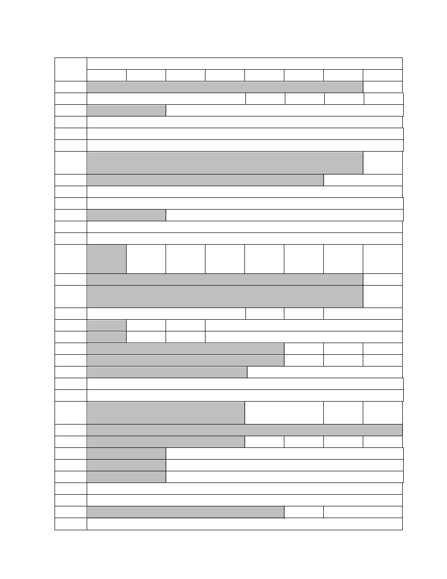
≠≠≠≠≠≠≠≠≠≠≠≠≠≠≠≠≠≠≠≠≠≠≠≠≠≠≠≠≠≠≠≠≠≠≠≠≠≠≠≠≠≠≠≠≠≠≠≠≠≠≠≠
35
STEL-2000A
REGISTER SUMMARY
Address
Contents
Bit 7
Bit 6
Bit 5
Bit 4
Bit 3
Bit 2
Bit 1
Bit 0
00
H
NCO Load
01
H
Integrate & Dump Filter Viewport Control
2’s C. Input
NCO C’In
Inv. LF
RXMSMPL
02
H
Receiver Baseband Sampling Rate Control
03-06
H
NCO Frequency Control Word (32 bits)
07-16
H
Matched Filter Acquisition/Preamble Symbol Coefficients
17-26
H
Matched Filter Data Symbol Coefficients
27
H
FEP
Disable
28
H
MF Viewport Control
29-2A
H
Acquisition/Preamble Symbol Threshold, Bits 9-0
2B-2C
H
Data Symbol Threshold, Bits 9-0
2D
H
Receiver Chips per Data Symbol
2E
H
Receiver Data Symbols per Burst, Bits 7-0
2F
H
Missed Detects per Burst Threshold
30
H
Rx Symb./
Burst Off
Missed
Det.
Per Bst. Off
Half Symb.
Pulse Off
B
’
pass
Max.
Power Sel.
Force Cont.
Acquis.
Manual
Punctual
Man. Det.
Enable
31
H
Man. Det.
32
H
Man.
Abort
33
H
AFC Viewport Control
LF Clr. Dis
Unused (0)
Signal Rotation Contrl.
34
H
Carry In
1/2
K2 On
K2 Gain Value
35
H
LF Freeze
K1 On
K1 Gain Value
36
H
Inv. O/p
BPSK En.
Rev. I & Q
37
H
Rx. En.
Tx En.
NCO En.
38
H
RXTEST
7-0
Read Address
39
H
Matched Filter Power Saver
3A
H
Receiver Data Symbols per Burst, Bits 15-8
3B
H
Receiver Overlay Sel.
IF Lpbk En
MF
LpbkEn
3C-3F
H
40
H
Inv. Symb.
TXMCHP
O’Bin. O/p
Tx BPSK
41
H
TXIFCLK Cycles per Chip
42
H
Tx Chips per Data Symbol
43
H
Tx Chips per Acquisition/Preamble Symbol
44-4B
H
Transmitter Acquisition/Preamble Symbol Code (64 bits)
4C-53
H
Transmitter Data Symbol Code (64 bits)
54
H
Set to 0
Transmitter Overlay Sel.
55-56
H
Transmitter Data Symbols per Burst, Bits 15-0

≠≠≠≠≠≠≠≠≠≠≠≠≠≠≠≠≠≠≠≠≠≠≠≠≠≠≠≠≠≠≠≠≠≠≠≠≠≠≠≠≠≠≠≠≠≠≠≠≠≠≠≠
STEL-2000A
36
Table 24. Register Summary

≠≠≠≠≠≠≠≠≠≠≠≠≠≠≠≠≠≠≠≠≠≠≠≠≠≠≠≠≠≠≠≠≠≠≠≠≠≠≠≠≠≠≠≠≠≠≠≠≠≠≠≠
37
STEL-2000A
ELECTRICAL CHARACTERISTICS
ABSOLUTE MAXIMUM RATINGS
Note: Stresses greater than those shown below may cause permanent damage to the
device. Exposure of the device to these conditions for extended periods may also affect
device reliability. All voltages are referenced to V
SS.
Symbol
Parameter
Range
Units
T
stg
Storage Temperature
–55 to +150
∞
C
V
DDmax
Supply voltage on V
DD
–0.3 to + 7
Volts
V
I(max)
Input voltage
–0.3 to V
DD
+0.3
Volts
I
i
DC input current
±
10
mA
RECOMMENDED OPERATING CONDITIONS
Symbol
Parameter
Range
Units
V
DD
Supply Voltage
+5
±
5%
Volts
T
a
Operating Temperature (Ambient)
0 to +70
∞
C
D.C. CHARACTERISTICS
Operating Conditions: V
DD
= 5.0 V
±
5%, V
SS
= 0 V, Ta = 0
∞
to 70
∞
C
Symbol
Parameter
Min.
Typ.
Max.
Units
Conditions
I
DDQ
Supply Current, Quiescent
5.0
mA
Static, no clock
I
DD
Supply Current, Operational
(Transmitter + Receiver)
380
170
mA
mA
f
RXIFCLK
= 45.056 MHz
f
RXIFCLK
= 20 MHz
I
DD
Supply Current, Operational
(Transmitter only,
f
RXIFCLK
= 0 MHz)
20
9
mA
mA
f
TXIFCLK
= 45.056 MHz
f
TXIFCLK
= 20 MHz
V
IH(min)
High Level Input Voltage
0.7 x V
DD
Volts
Logic '1'
V
IL(max)
Low Level Input Voltage
0.2 x V
DD
Volts
Logic '0'
I
IH(min)
High Level Input Current
10
µ
A
All inputs, V
IN
= V
DD
I
IL(max)
Low Level Input Current
–10
µ
A
TXIFCLK, RXIFCLK, RESET
––––––
only, V
IN
= V
SS
I
IL(max)
Low Level Input Current
–130
–45
–15
µ
A
All other inputs, V
IN
= V
SS
V
OH(min)
High Level Output Voltage
V
DD
– 0.4
V
DD
Volts
I
O
= –2.0 mA, All outputs
V
OL(max)
Low Level Output Voltage
0.2
0.4
Volts
I
O
= +2.0 mA, All outputs
C
IN
Input Capacitance
2
pF
All inputs
C
OUT
Output Capacitance
4
pF
All outputs
The typical operational supply current under various operating conditions can be calculated from the equation:
I
DD
= 5 x f
RXIFCLK
+ 13 x f
CHIP
mA
where f
RXIFCLK
is the frequency of RXIFCLK, and f
CHIP
is the chipping rate, both in MHz
Power = V
DD
x I
DD

≠≠≠≠≠≠≠≠≠≠≠≠≠≠≠≠≠≠≠≠≠≠≠≠≠≠≠≠≠≠≠≠≠≠≠≠≠≠≠≠≠≠≠≠≠≠≠≠≠≠≠≠
STEL-2000A
38
TRANSMITTER INPUT/OUTPUT TIMING
TXIFCLK
TXIN
t
CH
t
CL
t
SU
t
HD
t
CT
t
CT
TXCHPPLS
TXBITPLS,
TXTRKPLS,
TXACQPLS
DON'T CARE
VALID
DON'T CARE
TXIOUT,
TXQOUT
t
CT
TXIFOUT
A.C. CHARACTERISTICS
Operating Conditions: V
DD
= 5.0 V
±
5%, V
SS
= 0 V, T
a
= 0
∞
to 70
∞
C
Symbol
Parameter
Min.
Max.
Units
Conditions
f
TXIFCLK
TXIFCLK
Frequency (TXIFOUT not used)
45.056
20.0
MHz
MHz
STEL-2000A+45 only
STEL-2000A+20 only
f
TXIFCLK
TXIFCLK
Frequency (TXIFOUT in use)
20
MHz
Both speed grades
t
CH
TXIFCLK Pulse width, High
10
nsec.
t
CL
TXIFCLK Pulse width, Low
10
nsec.
t
SU
TXIN to TXIFCLK setup
3
nsec.
t
HD
TXIN to TXIFCLK hold
5
nsec.
t
CT
TXIFCLK to TXBITPLS , TXTRKPLS, TXACQPLS,
TXIOUT or TXQOUT delay
35
nsec.
Notes: 1. The number of TXIFCLK cycles per cycle of TXCHPPLS is determined by the data stored in bits 5-0 of
address 41
H
. It is shown as 2 in the above timing diagram but can be set from 2 to 64.
2. The width of the TXBITPLS , TXTRKPLS and TXACQPLS signal pulses is equal to the period of
TXCHPPLS; i.e., equal to the PN chip period.
3. In QPSK mode, the TXBITPLS signal pulses high twice during each symbol period, once during the center
chip and once during the last chip. If the number of chips per symbol is even, the number of chip periods
between the TXBITPLS pulse at the end of the previous symbol and the one in the center of the symbol
will be one more than the number of chip periods between the TXBITPLS pulse in the center of the symbol
and the one at the end. The falling edge of the second pulse corresponds to the end of the symbol period.
4. The TXTRKPLS signal pulses high once each symbol period, during the last chip period of that symbol.
The falling edge corresponds to the end of the symbol period.
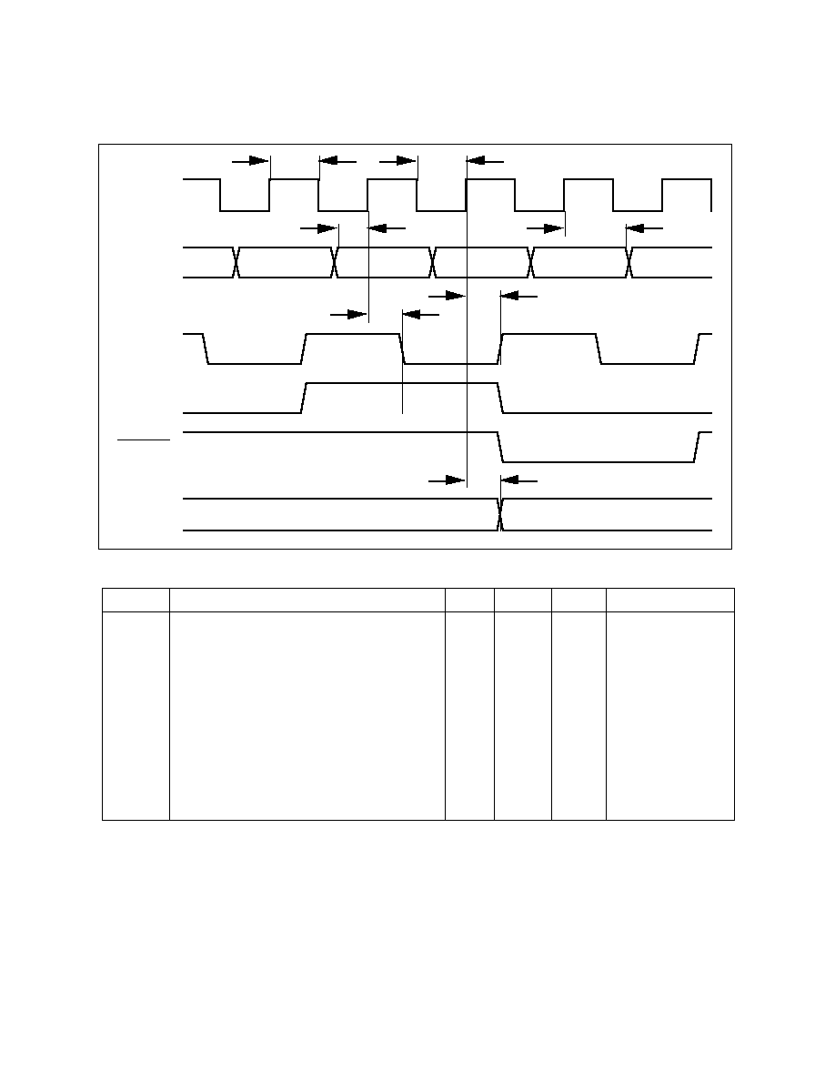
≠≠≠≠≠≠≠≠≠≠≠≠≠≠≠≠≠≠≠≠≠≠≠≠≠≠≠≠≠≠≠≠≠≠≠≠≠≠≠≠≠≠≠≠≠≠≠≠≠≠≠≠
39
STEL-2000A
5. The TXACQPLS signal pulses high once each burst, transmission, during the last chip of the Acquisi-
tion/Preamble symbol. The falling edge corresponds to the end of this symbol period.
RECEIVER INPUT/OUTPUT TIMING
RXIFCLK
RXIIN,
RXQIN
RXSPLPLS
RXSYMPLS
t
CH
t
CL
t
SU
t
HD
t
CR
t
CR
t
CD
RXDRDY
RXOUT,
RXIOUT,
RXQOUT
A.C. CHARACTERISTICS
Operating Conditions: V
DD
= 5.0 V
±
5%, V
SS
= 0 V, T
a
= 0
∞
to 70
∞
C,
Symbol
Parameter
Min.
Max.
Units
Conditions
f
RXIFCLK
RXIFCLK
Frequency
45.056
20.0
MHz
MHz
STEL-2000A+45 only
STEL-2000A+20 only
t
CH
RXIFCLK
Pulse width, High
10
nsec.
t
CL
RXIFCLK
Pulse width, Low
10
nsec.
t
SU
RXIIN
or RXQIN to RXIFCLK setup
3
nsec.
t
HD
RXIIN
or RXQIN to RXIFCLK hold
7
nsec.
t
CR
RXIFCLK
to RXSPLPLS, RXSYMPLS, or
RXDRDY
–––––––––
delay
35
nsec.
t
CD
RXIFCLK
to RXOUT, RXIOUT, or RXQOUT
delay
35
nsec.
Notes: 1. The number of RXIFCLK cycles per cycle of RXSPLPLS is determined by the data stored in bits 5-0 of
address 02
H
. It is shown as 2 in the above timing diagram but can be set from 2 to 64.
2. The rising edge of RXDRDY
–––––––––
should be used to clock out the data (RXOUT , RXIOUT, or RXQOUT).
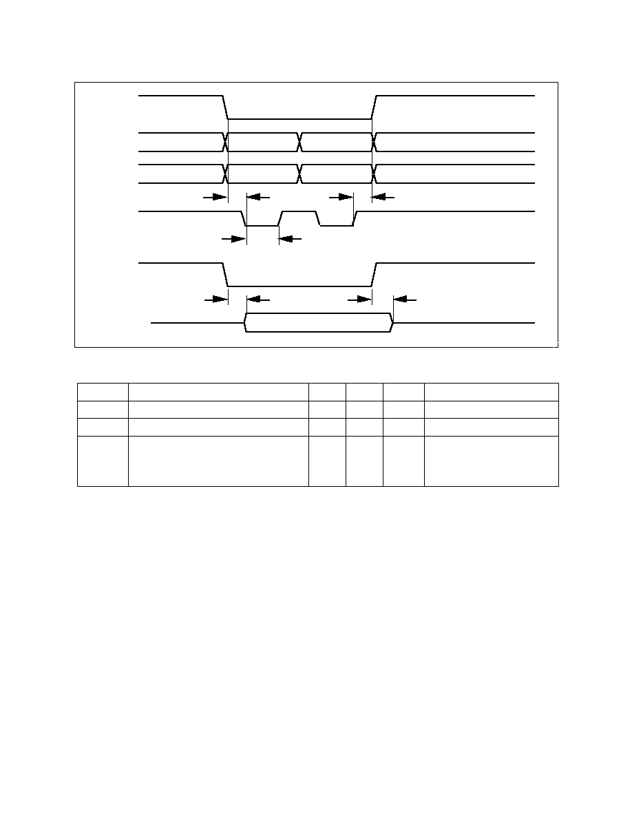
≠≠≠≠≠≠≠≠≠≠≠≠≠≠≠≠≠≠≠≠≠≠≠≠≠≠≠≠≠≠≠≠≠≠≠≠≠≠≠≠≠≠≠≠≠≠≠≠≠≠≠≠
STEL-2000A
40
RXTEST BUS AND MICROPROCESSOR INTERFACE TIMING
WRITE
CSEL
ADDR
6-0
DATA
7- 0
VALID
VALID
VALID
VALID
DON'T CARE
DON'T CARE
DON'T CARE
DON'T CARE
t
SU
t
HD
t
W
OEN
RXTEST
7-0
VALID
Hi-Z
Hi-Z
t
ZV
t
VZ
A.C. CHARACTERISTICS
Operating Conditions: V
DD
= 5.0 V
±
5%, V
SS
= 0 V, T
a
= 0
∞
to 70
∞
C,
Symbol
Parameter
Min.
Max.
Units
Conditions
t
SU
CSEL
–––––
, ADDR, DATA to WRITE setup
5
nsec.
t
HD
WRITE to CSEL
–––––
, ADDR, DATA hold
5
nsec.
t
W
WRITE
pulse width
5
nsec.
t
ZV
OEN
––––
low to RXTEST valid
3
12
nsec.
t
VZ
OEN
––––
high to RXTEST high impedance
2
8
nsec.
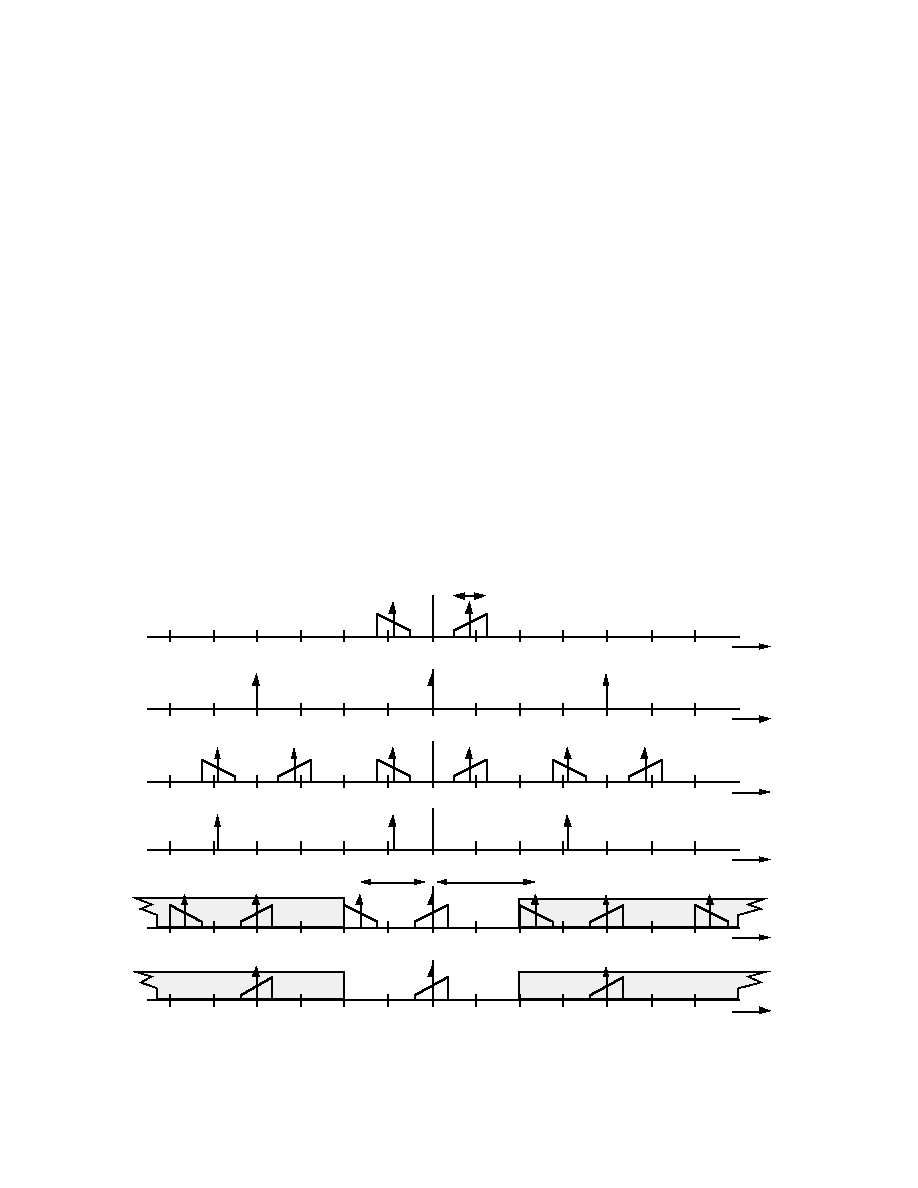
≠≠≠≠≠≠≠≠≠≠≠≠≠≠≠≠≠≠≠≠≠≠≠≠≠≠≠≠≠≠≠≠≠≠≠≠≠≠≠≠≠≠≠≠≠≠≠≠≠≠≠≠
41
STEL-2000A
APPENDIX I: THEORY OF OPERATION
Digital Downconversion
The STEL-2000A receiver’s downconverter circuitry
allows use of two distinct modes, where the mode
chosen will depend upon the application. In applica-
tions where the received PN chip rate is less than
approximately
1
/
8
of the I.F. sample clock (RXIFCLK)
rate, the STEL-2000A can be used with a single A/D
converter (ADC) and operate in Direct I.F. Sampling
Mode. For higher chip rate applications, it is neces-
sary to use the STEL-2000A in the full Quadrature
Sampling Mode; i.e., using a quadrature signal
source, two ADCs, and the on-chip NCO in its
quadrature mode.
Using the STEL-2000A with a Single ADC in Direct
I.F. Sampling Mode
Direct I.F. Sampling Mode allows one rather than two
ADCs to be used, as will be explained below. If
appropriate for the application, use of Direct I.F.
Sampling Mode can reduce the system cost since
quadrature downconversion or splitting and the sec-
ond ADC used in Quadrature Sampling Mode are not
required. The trade-off, however, is in the lower max-
imum PN chip rate that can be supported by the
STEL-2000A in Direct I.F. Sampling Mode as com-
pared to the maximum rate that can be supported by
Quadrature Sampling Mode.
In Direct I.F. Sampling Mode, the sampled signal is
presented as input to the receiver’s I channel input
(RXIIN) and the Q channel input (RXQIN) is held to
zero (where “zero” is defined by the ADC input for-
mat ). As a result, only two of the four multipliers in
the Downconverter’s complex multiplier are used and
the device does not make a true single-sideband
downconversion from I.F. to baseband. In Quadra-
ture Sampling Mode, by contrast, quadrature inputs
to two ADCs provide I and Q inputs to the STEL-
2000A and the full complex multiplier is used. An
illustration of the operation of Direct I.F. Sampling
Mode is shown in the frequency domain in Figure 7,
where the spectra have been drawn asymmetrically
so that spectral inversions can be readily identified.
The spectrum of a real input signal with center (I.F.)
frequency of f
1
and signal bandwidth B is shown in
line 1 of Figure 7. The bandwidth B is the two-sided
bandwidth, corresponding to a PN chip rate of
1/2
B
Mcps. Note that throughout this discussion it is
assumed that the signal bandwidth does not exceed
1/2
f
S A
; i.e., B <
1/2
f
SA
. Otherwise, the mixing and
sampling processes to be described will result in
destructive in-band aliasing. Also, clearly, the I.F.
frequency must be able to support the signal band-
width; i.e.,
1/2
B < f
1
.
FREQ.
INPUT SPECTRUM
BANDWIDTH: B
0
FREQ.
0
FREQ.
SPECTRUM
AFTER A/D
0
FREQ.
SPECTRUM AFTER IDEAL DIGITAL LOW PASS FILTER
0
FREQ.
QUADRATURE
NCO SPECTRUM
0
≠f
1
FREQ.
SPECTRUM AFTER MIXER
0
SPECTRUM OF
SAMPLING PROCESS
2 f
1
f
SA
≠2 f
1
f
SA
1
2
3
4
5
6
≠f
SA
f
SA
≠f
SA
f
SA
≠f
SA
f
SA
≠f
SA
f
SA
≠f
SA
≠f
1
f
1
≠f
1
f
1
Figure 7: Spectra of Signals in Direct I.F. Sampling Mode
The input signal is sampled at the frequency f
SA
,
where the sampling spectrum is shown in line 2 and
the resulting spectrum is shown in line 3. As can be
seen, the fundamental and harmonics of the sampling
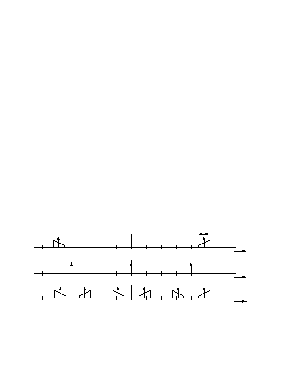
≠≠≠≠≠≠≠≠≠≠≠≠≠≠≠≠≠≠≠≠≠≠≠≠≠≠≠≠≠≠≠≠≠≠≠≠≠≠≠≠≠≠≠≠≠≠≠≠≠≠≠≠
STEL-2000A
42
frequency result in images of the input signal spec-
trum at other frequencies, where here the images are
centered about multiples of the sampling frequency.
In other words, the spectrum of the sampled signal
shown in line 3 contains aliases of the input signal at
frequencies f
1
±
n f
SA
, where n can assume both posi-
tive and negative integer values. Since the sampling
process is linear, no spectral inversion occurs; i.e., the
original spectrum is translated along the frequency
axis with no mirror reflections of the input spectrum
created.
The STEL-2000A’s NCO provides a quadrature (sine
and cosine) output that defines a complex signal.
Line 4 shows its spectrum as an impulse at frequency
-f
1
, where the minus sign reflects the signal’s use in
downconversion and the absence of a positive
impulse at frequency +f
1
results because the NCO
output is truly complex. Aliases of this impulse are
shown offset by integer multiples of f
SA
to reflect the
sampled nature of the NCO output. When the input
sampled signal of line 3 is then modulated with the
complex signal of the STEL-2000A’s quadrature NCO
of line 4, the signal spectrum after mixing is as shown
in line 5. The sections shown inside the shaded areas
are the aliases of the baseband signal beyond the
Nyquist frequency and are not of concern. The sig-
nals inside the primary baseband Nyquist region
(| f | <
1/2
f
SA
) consist of the desired signal and a
spectrally reversed or inverted image signal with cen-
ter frequency separated from that of the desired
signal by 2 f
1
, twice the I.F. frequency before
sampling. This image signal can be removed by a
subsequent ideal lowpass filter as shown in line 6.
In Figure 7 the input signal is shown at a low I.F. fre-
quency such that f
1
<
1 /2
f
SA
; i.e., the signal is only
defined inside the primary Nyquist region. Provided,
however, that B <
1 /2
f
SA
, that condition need not be
true as long as the input spectrum is only defined for
frequencies within a non-primary Nyquist region; i.e.,
defined only over frequencies f such that:
(n -
1 /2
) f
SA
< | f | < (n +
1 /2
) f
SA
for positive integer
values of n. Direct I.F. Sampling Mode with this type
of signal is shown in Figure 8, where it can be seen
that in line 3 the diagram’s high frequency input has
the same spectrum after sampling as does the low fre-
quency input in Figure 7; consequently, all subse-
quent operations are identical to those in Figure 7.
This result stems from the periodic nature of sam-
pling: sampling an input frequency f
1
is theoretically
indistinguishable from sampling an input frequency
(n f
SA
+ f
1
) for positive integer n and positive f
1
<
1/ 2
f
SA
. A slightly different result obtains, however,
when sampling an input frequency (n f
SA
- f
1
), again
for positive integer n and positive f
1
<
1/ 2
f
SA
. In this
case, the positions of the spectrally inverted and spec-
trally correct aliases will be interchanged when com-
pared with an input frequency of (n f
SA
+ f
1
). As a
consequence, the desired baseband signal after down-
conversion and filtering will also be spectrally
inverted. This phenomenon is equivalent to high-side
conversion; i.e., downconversion of a signal by means
of a local oscillator at a frequency higher than the car-
rier frequency. If the modulation type is QPSK,
demodulation of a spectrally inverted signal will
result in the inversion of the Q channel data (which
can be readily corrected); if the modulation type is
BPSK, there is no effect on the demodulated data.
The above discussion has assumed ideal lowpass fil-
tering to recover the desired signal at baseband, but,
in the STEL-2000A’s Downconverter, an ideal
lowpass filter is not available. The quadrature
Integrate and Dump filter of the Downconverter
serves this purpose instead. The Downconverter’s
I n t e g r a t e a n d D u m p
FREQ.
INPUT SPECTRUM
BANDWIDTH: B
0
FREQ.
0
FREQ.
SPECTRUM
AFTER A/D
0
SPECTRUM OF
SAMPLING PROCESS
1
2
3
≠f
SA
≠ f
1
f
SA
+ f
1
f
SA
≠f
SA
f
SA
≠f
SA
≠f
1
f
1
Figure 8: Direct I.F. Sampling Mode With I.F.
Frequency (fSA + f1) > Sampling Frequency fSA
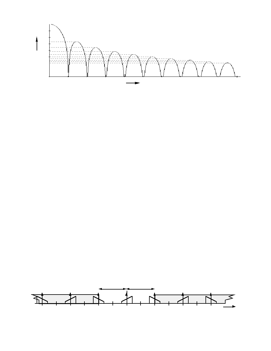
≠≠≠≠≠≠≠≠≠≠≠≠≠≠≠≠≠≠≠≠≠≠≠≠≠≠≠≠≠≠≠≠≠≠≠≠≠≠≠≠≠≠≠≠≠≠≠≠≠≠≠≠
43
STEL-2000A
Gain
dB
≠10
≠15
≠20
≠25
≠30
≠35
≠40
≠5
0
0
1
2
3
4
5
Nf / f
SA
Figure 9: G(
) = sin(
’)/
’, where
’ = (2
Nf)/f
SA
filter is a decimation filter, integrating input samples
over a programmable number of sample periods, N,
so that the output sampling rate is (
1
/
N
)
th
of the input
sampling rate and the I.F. sampling rate f
SA
is deci-
mated to the baseband sampling rate. Since the STEL-
2000A’s PN Matched Filter requires two samples per
chip, the baseband sampling rate must be at twice the
PN chip rate and N must equal f
SA
/B. When the
sampling rate is much greater than the signal band-
width (or, equivalently, the chip rate), the Integrate
and Dump filter is most effective in attenuating the
unwanted aliased image. This performance can be
seen from the transfer function G(
) of a decimation
filter, where:
G(
) = sin(
’)/
’ and
’ = (2
Nf)/f
SA
.
Figure 9 shows a plot of the gain of this transfer func-
tion as a function of the normalized frequency
(Nf/f
SA
). To effect the desired low pass filter and
eliminate the aliased image in the baseband Nyquist
region appearing in line 5 of Figure 7, the attenuation
must be suitably high for frequencies greater than, in
the worst case,
1/2
B. Given a defined signal band-
width B, however, judicious choice of f
1
and f
S A
allows a higher break frequency to be chosen, as will
be discussed. As an extreme worst case, if f
1
=
1 /4
f
SA
and B =
1/ 2
f
SA
, corresponding to the highest chip rate
that can be handled for a given value of f
SA
, then the
break frequency must be
1 /2
B (equal to
1 /4
f
SA
). In
this example, then, N = f
SA
/B = 2 and the attenuation
provided by the Integrate and Dump filter is given by
the curve of Figure 9 for values of (N f / f
SA
) greater
than
1 /2
. As can be seen, the attenuation will be at
least equal to the peak of the corresponding lobe or at
least ~13 dB. This sidelobe peak is a worst case, and
much of the alias energy outside the desired band will
be attenuated by more than 13 dB. Nonetheless, the
presence of unattenuated energy from the unwanted
alias degrades performance. It is for this reason that
Direct I.F. Sampling Mode is only recommended for
received PN chip rates less than
1 /8
f
SA
; in other
words, for B <
1/ 4
f
SA
. The attenuation realized by the
Integrate and Dump filter is then further determined
by the choice of the I.F. frequency f
1
and the I.F.
sampling rate f
SA
.
The choice of the I.F. frequency and sampling rate is
crucial so that the unwanted alias of the signal in the
baseband Nyquist region lies as far as possible from
the desired signal to permit maximum attenuation.
The optimum separation of the desired signal and the
unwanted alias occurs when the alias is centered at
the bounds of the baseband Nyquist region,
| f | =
1
/
2
f
SA
as shown in Figure 10. In this case, the
desired signal is equally spaced from the unwanted
aliases in both the positive and negative frequency
domains and f1 =
1
/
4
f
SA
. Consider, then, the worst
case appropriate for Direct I.F. Sampling Mode. If
B <
1 /4
f
SA
as has been said to be appropriate for
Direct I.F. Sampling Mode, then N = f
SA
/B = 4, the
break frequency is
3 /8
f
SA
or greater, and the attenua-
tion provided by the Integrate and Dump filter is
given by the curve of Figure 9 for values of (N f / f
SA
)
greater than
3 /2
. Here, the attenuation is at least ~21
dB, offering much better attenuation of the unwanted
alias than in the previous worst case example. Fur-
ther analysis shows that if the input SNR is 15 dB,
then the alias attenuated by 21 dB will reduce the
SNR by approximately 1 dB.
FREQ.
SPECTRUM AFTER MIXER
2 f
1
f
SA
≠ 2 f
1
5
≠f
SA
f
SA
Figure 10: Optimum Condition for Bandpass Sampling
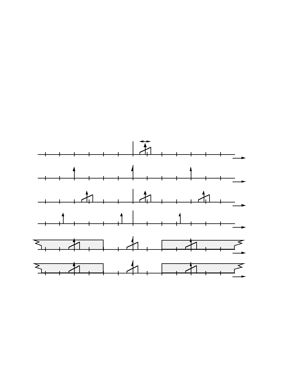
≠≠≠≠≠≠≠≠≠≠≠≠≠≠≠≠≠≠≠≠≠≠≠≠≠≠≠≠≠≠≠≠≠≠≠≠≠≠≠≠≠≠≠≠≠≠≠≠≠≠≠≠
STEL-2000A
44
The optimum choice of I.F. frequency discussed above
can be extended beyond the primary Nyquist region.
Since an I.F frequency of n f
SA
+ f
1
produces exactly
the same result for any value of n, the general condi-
tion for optimum separation of the desired signal and
the unwanted alias is:
f1 = n f
SA
+
1
/
4
f
SA
; B<
1
/
2
f
SA
for positive integer n and positive B and f
1
.
And, if care is taken to handle the effect of high side
conversion, the following I.F. frequencies also fulfill
the optimum condition:
f1 = n f
SA
-
1
/
4
f
SA
; B<
1
/
2
f
SA
for positive integer n and positive B and f
1
.
Using the STEL-2000A with Two ADCs in
Quadrature Sampling Mode
Quadrature Sampling Mode requires that quadrature
I and Q channel I.F. inputs are sampled by two ADCs
and input to the STEL-2000A’s Downconverter. All
four multipliers of the Downconverter’s complex
multiplier are then used to perform true single side-
band downconversion to baseband. Quadrature
inputs imply that the input signal is complex, and the
input signal spectrum shown in line 1 of Figure 11 is
thus only defined for positive frequencies. As a
result, the image alias within the primary Nyquist
region associated with Direct I.F. Sampling Mode
does not appear and does not have to be attenuated
by the Integrate and Dump filter. As in the prior dis-
cussion, this analysis holds as long as B <
1 /2
f
SA
,
1 /2
B
< f
1
, and the input spectrum is only defined for fre-
quencies within a single Nyquist region; i.e., defined
only over frequencies f such that:
(n -
1 /2
) f
SA
< | f | < (n +
1 /2
) f
SA
for positive integer
values of n.
FREQ.
FREQ.
FREQ.
FREQ.
FREQ.
FREQ.
INPUT SPECTRUM
BANDWIDTH: B
0
0
SPECTRUM
AFTER A/D
0
SPECTRUM AFTER IDEAL DIGITAL LOW PASS FILTER
0
QUADRATURE
NCO SPECTRUM
0
SPECTRUM AFTER MIXER
0
SPECTRUM OF
SAMPLING PROCESS
1
2
3
4
5
6
≠f
1
f
SA
≠f
SA
f
SA
≠f
SA
f
SA
≠f
SA
f
SA
≠f
SA
f
SA
≠f
SA
≠f
1
f
1
≠f
1
f
1
Figure 11: Spectra of Signals in Quadrature Sampling Mode

≠≠≠≠≠≠≠≠≠≠≠≠≠≠≠≠≠≠≠≠≠≠≠≠≠≠≠≠≠≠≠≠≠≠≠≠≠≠≠≠≠≠≠≠≠≠≠≠≠≠≠≠
45
STEL-2000A
Differential Demodulation
As noted in the preceding text, computation of the
“dot” and “cross” products is fundamental to opera-
tion of the DPSK Demodulator and Frequency Dis-
criminator. Let I
k
and Q
k
represent the I and Q chan-
nel inputs, respectively, for the k
th
symbol after
downconversion and despreading. The dot and cross
products can then be defined as:
Dot(k)
= I
k
I
k-1
+ Q
k
Q
k-1
; and,
Cross(k) = Q
k
I
k-1
- I
k
Q
k-1
.
In the complex domain, these products can be seen to
have been defined to form the complex conjugate
product between two input samples, one symbol
apart. Let the k
th
input sample, s
in
(k), be defined as:
s
in
(k)
I(k) + j Q(k),
where I(k) and Q(k) are the 8-bit peak power PN
Matched Filter I and Q channel outputs directed to
the DPSK Demodulator. In polar form, s
in
(k) may be
conveniently defined as:
s
in
(k)
A(k).e
jØ(k)
with
A(k)
I
2
(k)+Q
2
(k)
Ø(k)
arctan
Q(k)
I(k) .
Simple substitution then shows that the complex
conjugate product between consecutive symbols
(with an arbitrary phase shift introduced to the
previous symbol value) may be expressed as::
s
out
(k)
= s
in
(k) . [s
in
(k–1) .
fixed
]
*
Dot(k) + j Cross(k)
where
fixed
= arbitrary fixed phase rotation;
Dot(k)
= Re[s
out
(k)]; and,
Cross(k) = Im[s
out
(k)].
The fixed phase rotation
fixed
has been introduced to
later simplify the decision criteria, but the ability to
express real and imaginary parts of the complex con-
jugate product between consecutive symbols with the
dot and cross products is the key to their use in
DPSK demodulation.
BPSK Demodulation
In DPSK, the phase difference between successive
samples is due to the data modulation phase differ-
ences,
Ø
m o d
, plus any induced phase rotation
between symbols,
Ø
rot
, resulting from, for example,
a frequency offset between the received signal’s I.F.
and that provided by the Downconverter. For
DBPSK, the data modulation differences
Ø
mod
can
take only the values of 0
∞
or 180
∞
. Expressing the
complex phase difference [Ø(k)-Ø(k-1)] in terms of
these components, the decision can be seen to be
based on:
s
out
(k) = A(k).A(k-1).e
jØ(k).
e
-jØ(k-1)
=
A(k).A(k-1).e
j[
Ømod(k) +
Ørot(k) ]
For DBPSK, only the real part of s
out
(k), Dot(k), is
needed to determine the modulated phase transition:
Dot(k) = A(k).A(k-1).cos(
Ø
mod
(k)+
Ø
rot
(k))
=
±
A(k).A(k-1).cos(
Ø
rot
(k))
where the sign is determined by the transmitted data
since cos[
Ø
mod
(k)] =
±
1. As a result,
Dot(k)
±
A
2
(k)
if the amplitude of the signal is constant for consecu-
tive symbols and if the phase rotation
Ø
r o t
(k)
between symbols is small. The STEL-2000A DPSK
Demodulator can thus use the sign of the dot product
in order to make DBPSK symbol decisions without
the introduction of any fixed phase rotation.
QPSK Demodulation
For DQPSK modulation, the possible phase shifts
between successive symbols due to the modulation
are 0
∞
, 90
∞
, 180
∞
, and 270
∞
. Here, introduction of a
phase shift (
fixed
) of
±
45
∞
to the previous symbol in
the calculation of the dot and cross products is
desired in order shift the possible phase differences to
45
∞
, 135
∞
, 225
∞
, or 315
∞
so that the DQPSK decision
boundaries coincide with the signs of the dot and
cross products. In the STEL-2000A DPSK demodula-
tor, phase rotation is accomplished in the signal rota-
tion block by the following transformation of the I
and Q channel values::
I
rot
(k)
= [ I(k) - Q(k) ]/2 for 45
∞
rotation
I
rot
(k)
= [ I(k) + Q(k) ]/2 for -45
∞
rotation
Q
rot
(k)
= [ I(k) + Q(k) ]/2 for 45
∞
rotation
Q
rot
(k)
= -[ I(k) + Q(k) ]/2 for -45
∞
rotation
The divide by 2 is part of the signal rotation function.
This transformation is equivalent to multiplying by (1
±
j)/2 or (1/
2)ej
Ø(fixed)
where Ø
fixed
is
±
45
∞
. In this
case, s
out
(k) becomes:
s
out
(k)
= A(k).A(k-1).e
jØ(k).
e
-jØ(k-1).
[
fixed
]
*
=
A(k).A(k-1).e
j[
Ømod(k) +
Ørot(k) ].
(1/
2)ej
Ø(fixed)

≠≠≠≠≠≠≠≠≠≠≠≠≠≠≠≠≠≠≠≠≠≠≠≠≠≠≠≠≠≠≠≠≠≠≠≠≠≠≠≠≠≠≠≠≠≠≠≠≠≠≠≠
STEL-2000A
46
so that
Dot(k)
(1/
2)A(k).A(k-1).cos(
Ø
mod
(k) - Ø
fixed
)
Cross(k)
(1/
2)A(k).A(k-1).sin(
Ø
mod
(k) - Ø
fixed
)
where the phase rotation
Ø
rot
(k) due to the fre-
quency offset between symbols has been assumed
negligible.
A summary of the Dot(k) and Cross(k) products for
the possible values of
Ø
mod
(k) and Ø
fixed
is shown
below, illustrating how the sign of the dot and cross
products allow the symbol decision to be made:
Ø
fixed
= -45
∞
Ø
fixed
= +45
∞
Ø
mod
(k)
Dot(k)
Cross(k
)
Dot(k)
Cross(k
)
0
∞
+A
2
+A
2
+A
2
-A
2
90
∞
-A
2
+A
2
+A
2
+A
2
180
∞
-A
2
-A
2
-A
2
+A
2
270
∞
+A
2
-A
2
-A
2
-A
2
Table 25. Dot and Cross Product Summary
DQPSK Demodulation
The STEL-2000A DPSK Demodulator decision logic is
designed so that correct DQPSK decisions are made
with a signal rotation of Ø
Fixed
= -45
∞
. For
/4 QPSK
modulation, however, the modulator itself inserts 45
∞
between consecutive symbols, and the possible phase
shifts between successive symbols due to modulation
are 45
∞
, 135
∞
, 225
∞
, and 315
∞
. As a result, the DPSK
Demodulator should be configured for
/4 QPSK
with Ø
Fixed
= 0
∞
.
Frequency Error Signal Generation
The frequency discriminator function or error signal
can similarly be generated based on the dot and cross
products. The objective is an error signal reflecting
the sine of the phase difference between the present
and prior symbol after correcting for the estimated
phase increments due to data modulation. In the
STEL-2000A Frequency Discriminator, the frequency
error is calculated through a decision-directed cross-
product algorithm and is then used with the Loop Fil-
ter to correct the NCO frequency. Assuming an input
s
in
(k), where:
s
in
(k) = I(k) + j Q(k),
the algorithm calculates the frequency discriminator
function for DBPSK, s
AFC/BPSK
(k), as:
s
AFC/BPSK
(k) = SIGN[Dot(k)] . Cross(k)
= SIGN[Dot(k)] . A(k).A(k-1).sin(Ø(k)-Ø(k-1))
= SIGN[Dot(k)].A(k).A(k-1).sin(
Ø
mod
(k)+
Ø
rot
(k))
SIGN[Dot(k)] . A
2
(k).cos[
Ø
mod
(k)].sin[
Ø
rot
(k)]
A
2
(k).sin[
Ø
rot
(k)].
The final result assumes that the amplitude of the sig-
nal is constant over consecutive symbols and shows
that the discriminator function is directly related to
the change in phase between successive symbols.
Since the interval between successive symbols is
fixed, the discriminator function can be interpreted as
a frequency error signal.
For DQPSK signals, the STEL-2000A computes the
discriminator function s
AFC/QPSK
(k) as:
s
AFC/QPSK
(k) =
SIGN[Dot(k)].Cross(k).SIGN[Cross(k)].Dot(k)
where the above expression can be reduced to the
same as for DBPSK,
s
AFC/QPSK
(k)
A
2
(k).sin(
Ø
rot
(k)).

≠≠≠≠≠≠≠≠≠≠≠≠≠≠≠≠≠≠≠≠≠≠≠≠≠≠≠≠≠≠≠≠≠≠≠≠≠≠≠≠≠≠≠≠≠≠≠≠≠≠≠≠
47
STEL-2000A
Using the Modulator in the STEL-2000A Transmitter
The STEL-2000A incorporates a Direct Digital Synthe-
sizer (DDS) based BPSK/QPSK modulator which can
be used to generate the transmit output signal at some
IF frequency, thereby eliminating the need for a sepa-
rate modulator. Because it is a sampled data system,
like the other parts of the system, care must be taken
to ensure that the results of aliasing do not adversely
affect the transmit signal. The sampling clock for the
modulator is f
RXIFCLK
, since the NCO is driven by this
clock, and for this reason both TXIFCLK and
RXIFCLK must be common when the modulator is
being used. When a DDS is used to generate an un-
modulated signal the results are easy to predict
because the stepped sinewave generated by the DDS
has spectral lines at the frequencies n.f
CLK
±
f
OUT
for
all integer values of n. However, when the DDS sig-
nal is modulated with a series of rectangular pulses
each one of these spectral lines is replaced by a sinc
function (i.e., sin(x)/x), the spectrum of the modulat-
ing signal itself, each with a very significant band-
width. Any part of the spectrum of the baseband
component (i.e. the one where n = 0 in the equation
n.f
CLK
±
f
OUT
) above the Nyquist frequency (f
CLK
/2)
results in its first alias (i.e. the one where n = 1 in the
equation n.f
CLK
±
f
OUT
) intruding below the Nyquist
frequency, and this may interfere with the desired
signal. This is called aliasing distortion. A typical
example is shown in Figure 12.
The baseband component is shown as a the thick
curve and the first alias is shown as the lighter curve;
the higher order aliases are ignored for simplicity.
Note that in this example the nulls between the side-
lobes of the baseband signals coincide with those of
the first alias; this is simply the result of the numbers
chosen, and this will not occur in all cases. In a practi-
cal system the output signal would typically be fil-
tered to eliminate the sidelobes, as well as the signals
above the Nyquist frequency. As can be seen, the
second and third sidelobes of the first alias fall right
into this band of the spectrum, distorting the desired
signal. The magnitude of this signal at the peak of the
sidelobes is approximately –18 dBc. Clearly some
improvement can be obtained by choosing a carrier
frequency that increases the separation of the base-
band main lobe from the first alias main lobe, as
shown in Figure 13.
Nyquist
Frequency
2 x C
R
0
≠13
≠18
≠21
≠23
≠25
dB
Frequency/f
TXIFCLK
0
0.1
0.2
0.3
0.4
0.5
0.6
0.7
0.8
Figure 12: Spectrum of DDS modulated at 0.1 x f
RXIFCLK
when carrier frequency is set to 0.4 x f
RXIFCLK
Nyquist
Frequency
0
≠13
≠18
≠21
≠23
≠25
dB
Frequency/f
TXIFCLK
0
0.1
0.2
0.3
0.4
0.5
0.6
0.7
0.8
2 x C
R
Figure 13: Spectrum of DDS modulated at 0.1 x f
RXIFCLK
when carrier frequency is set to 0.25 x f
RXIFCLK
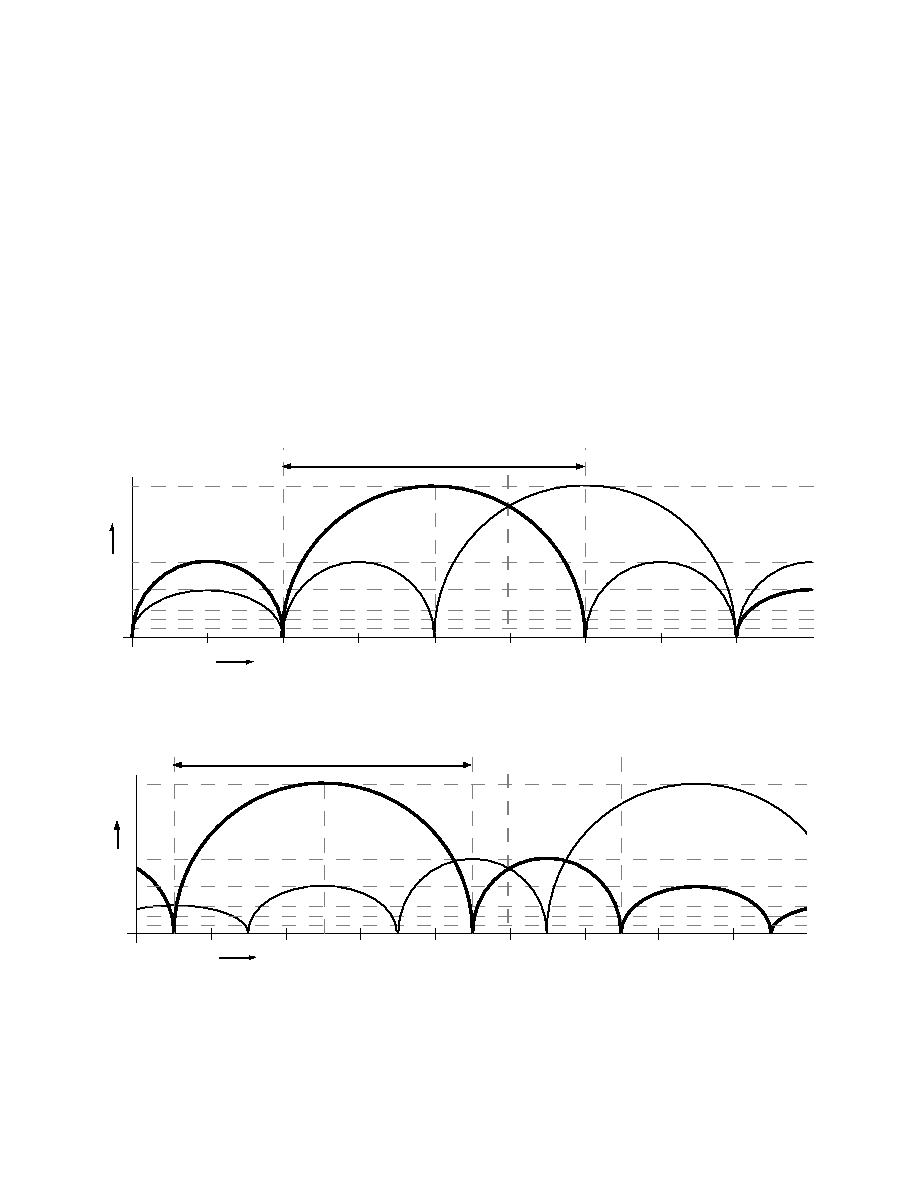
≠≠≠≠≠≠≠≠≠≠≠≠≠≠≠≠≠≠≠≠≠≠≠≠≠≠≠≠≠≠≠≠≠≠≠≠≠≠≠≠≠≠≠≠≠≠≠≠≠≠≠≠
STEL-2000A
48
In this case the carrier frequency has been reduced to
0.25 x f
RXIFCLK
and now the fourth and fifth sidelobes
of the first alias fall in the same part of the spectrum
as the baseband main lobe, reducing the distortion to
approximately –23 dBc at the peak of the sidelobe.
In both of the cases shown above, especially the sec-
ond, the level of the distortion is low enough that the
performance penalty would not be very great since
the effective distortion is reduced by the processing
gain in the despreader. However, in both of these
cases the chipping rate was a very modest 10% of the
frequency of the system clocks; if the chipping rate is
increased to 40% the situation is very different, as
shown in Figure 14.
Here, both the chipping rate and the carrier frequency
have been set at 20% of the clock frequency and now
the baseband main lobe straddles the Nyquist fre-
quency. Consequently, the first alias of the main lobe
overlaps the spectrum of the baseband main lobe,
resulting in very sig nificant aliasing distortion which
cannot be eliminated by filtering. This would
severely effect the performance of the system and in
general will be completely unacceptable. Reducing
the carrier frequency to 25% of the clock dramatically
reduces the distortion level again, as shown in Figure
15.
Although the distortion is still fairly severe, adequate
performance may still be obtainable as a result of the
processing gain, but the performance would be many
dBs off the theoretical limit. The conclusion is that as
the chipping rate of the system increases so does the
effect of the aliasing distortion in the modulator, and
the performance will degrade. A practical limit may
be in the region of 15% of the clock frequency, but in
reality every case is unique and should be evaluated
before deciding to use the internal DDS modulator.
Nyquist
Frequency
0
≠13
≠18
≠21
≠23
≠25
dB
Frequency/f
TXIFCLK
0
0.1
0.2
0.3
0.4
0.5
0.6
0.7
0.8
2 x C
R
Figure 14: Spectrum of DDS modulated at 0.4 x f
RXIFCLK
when carrier frequency is set to 0.4 x f
RXIFCLK
0
dB
Nyquist
Frequency
Frequency/f
TXIFCLK
0.1
0.2
0.3
0.4
0.5
0.6
0.7
0.8
≠13
≠18
≠21
≠23
≠25
0
2 x C
R
Figure 15: Spectrum of DDS modulated at 0.4 x f
RXIFCLK
when carrier frequency is set to 0.25 x f
RXIFCLK
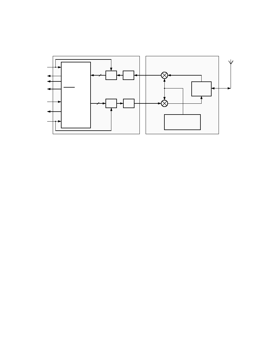
≠≠≠≠≠≠≠≠≠≠≠≠≠≠≠≠≠≠≠≠≠≠≠≠≠≠≠≠≠≠≠≠≠≠≠≠≠≠≠≠≠≠≠≠≠≠≠≠≠≠≠≠
49
STEL-2000A
APPENDIX II: TYPICAL APPLICATION
SPREAD SPECTRUM BPSK/QPSK TRANSCEIVER
STEL-2000A
LPF
A / D
R F
TR A N S-
C EIV ER
FIX ED
O SC ILLA TO R
(U p/ D ow n C onv er t er )
D A TA
O U T
D A TA
IN
TX
C LO C K
4x TX
C H IP
C LO C K
R X
C LO C K
4x R X
C LO C K
LINEAR RF MODULE
R X IIN
T X IFOUT
R X IFC LK
R X IOUT
R X D R D Y
T X IN
T X B IT P LS
T X IFC LK
R X QOUT
LPF
D / A
8
8
BASEBAND MODULE
Figure 16: Spread Spectrum BPSK/QPSK Transceiver
≠≠≠≠≠≠≠≠≠≠≠≠≠≠≠≠≠≠≠≠≠≠≠≠≠≠≠≠≠≠≠≠≠≠≠≠≠≠≠≠≠≠≠≠≠≠≠≠≠≠≠≠≠≠≠≠≠≠≠≠≠≠≠≠≠≠

Copyright © Intel Corporation, December 15, 1999.
All rights reserved
Information in this document is provided in connection with
IntelÆ products. No license, express or implied, by estoppel
or otherwise, to any intellectual property rights is granted by
this document. Except as provided in Intels Terms and Con-
ditions of Sale for such products, Intel assumes no liability
whatsoever, and Intel disclaims any express or implied
warranty, relating to sale and/or use of IntelÆ products in-
cluding liability or warranties relating to fitness for a particu-
lar purpose, merchantability, or infringement of any patent,
copyright or other intellectual property right. Intel products
are not intended for use in medical, life saving, or life sus-
taining applications.
Intel may make changes to specifications and product de-
scriptions at any time, without notice.
For Further Information Call or Write
INTEL CORPORATION
Cable Network Operation
350 E. Plumeria Drive, San Jose, CA 95134
Customer Service Telephone: (408) 545-9700
Technical Support Telephone: (408) 545-9799
FAX: (408) 545-9888