Document Outline
- FEATURES
- FUNCTIONAL DESCRIPTION
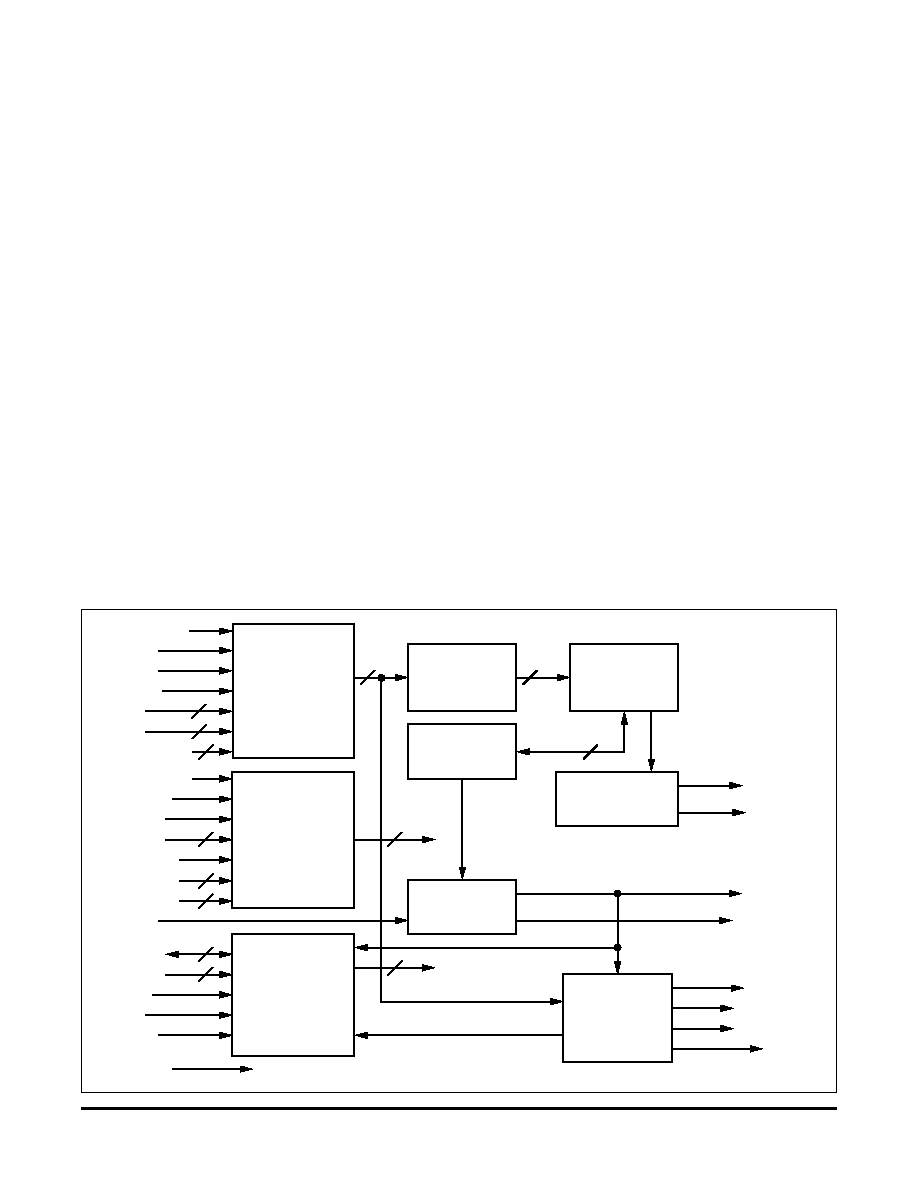
- BLOCK DIAGRAM
- PIN CONFIGURATION
- INPUT SIGNALS
- OUTPUT SIGNALS
- threshold value.
- INPUT (WRITE) FUNCTIONS
- OUTPUT (READ) FUNCTIONS
- MICROPROCESSOR INTERFACE MEMORY MAP
- PUNCTURED MODE OPERATION
- ELECTRICAL CHARACTERISTICS
- TIMING. RATE 1 /2 AND EXTERNAL DEPUNCTURING
- A.C. CHARACTERISTICS
- PUNCTURED SYMBOL SEQUENCES
- INTERNAL DEPUNCTURING TIMING. RATE 2 /3 SHOWN
- EXTERNAL DEPUNCTURING TIMING. RATE 3 /4 SHOWN
- MICROPROCESSOR INTERFACE TIMING
- NODE SYNCHRONIZATION
- NODE SYNC TIMING
- NODE SYNC SEQUENCES
- BER PERFORMANCE
- APPLICATION INFORMATION

R
STEL-2060C/CR
45 Mbps
Viterbi Decoder
STEL-2060C/CR
Data Sheet
STEL-2060C
2
FUNCTIONAL DESCRIPTION
Convolutional encoding and Viterbi decoding are used to
provide forward error correction (FEC) which improves
digital communication performance over a noisy link. The
STEL-2060C is a specialized product designed to perform
this specific communications related function. At the
encoder a stream of symbols is created which introduces a
high degree of redundancy. This enables accurate decoding
of the information despite a high symbol error rate resulting
from an impaired communications link.
The STEL-2060C contains a K = 7 Viterbi Decoder. The data
inputs can be in offset binary or offset signed-magnitude
formats, with 3-bit soft decision. Auto node sync is provided
for applications where symbol uncertainty can occur. Rate
2
/
3
,
3
/
4
,
4
/
5
,
5
/
6
,
6
/
7
and
7
/
8
punctured signals can be
decoded, as well as non-punctured, Rate
1
/
2
, signals. The
polynomials and puncturing patterns used are industry
standards. Depuncturing logic is incorporated into the
decoder to provide automatic depuncturing of received data
at rates
2
/
3
,
3
/
4
and
7
/
8
when the puncturing patterns
supported by the device are used. A BER monitor is also
provided in the device, along with a circuit for computing
the mean value of the BER over an extended period. These
circuits operate with punctured codes as well as
unpunctured. The STEL-2060C incorporates a descrambler
for signals scrambled with the "Invert G2" algorithm. (With
this method the G2 symbols are logically inverted at the
encoder. This provides a very effective level of scrambling
for the purpose of avoiding long strings of ones or zeroes in
the transmitted signal using BPSK modulation.)
FEATURES
s
45 Mbps Operating Rate
s
Constraint Length K = 7
G
1
= 171
8
G
2
= 133
8
s
Multiple Rates: Rate
1
/
2
as well as
Punctured codes at Rates
2
/
3
through
7
/
8
s
Internal Depuncturing Capability at Rates
2
/
3
,
3
/
4
and
7
/
8
s
Multiple Devices can be Multiplexed to
Give Higher Data Rates
s
Optimized Interface to Operate with BPSK
and QPSK Demodulators
s
Auto Node Sync Capability
s
Differential Decoder
s
"Invert G2" Descrambler
s
Internal BER Monitor and BER
Measurement Circuit
s
5.2 dB Coding Gain @10
-5
BER (R =
1
/
2
)
s
100-pin PQFP Package
s
0.5 Micron CMOS Technology
BLOCK DIAGRAM
SYMBOL
ALIGNMENT
AND
DEPUNCTURING
CIRCUIT
BRANCH
METRIC
ASSIGNMENT
VITERBI
DECODER
(ACS)
TRACEBACK
MEMORY
TIMING AND
CONTROL
G1
G2
PNCG1/G2
DCLKIN
DIFFERENTIAL
DECODER
DATO
AUTO
SYNC
BER
MONITOR
AND
COUNTER
BERR
SYMCKIN
G1ERR
G2ERR
OOS
ODCLK
DDIF
RESET
LDG2
PARL
OBIN
ADDR
INT
3
8
2
3
3
DATA
NODE SYNC
CONTROL
TO ALL REGISTERS
µP
INTERFACE
RD
CSEL
WR
RATE
EXTSEL
3
DSCRAM
COUNT
8
THRES
H
8
3
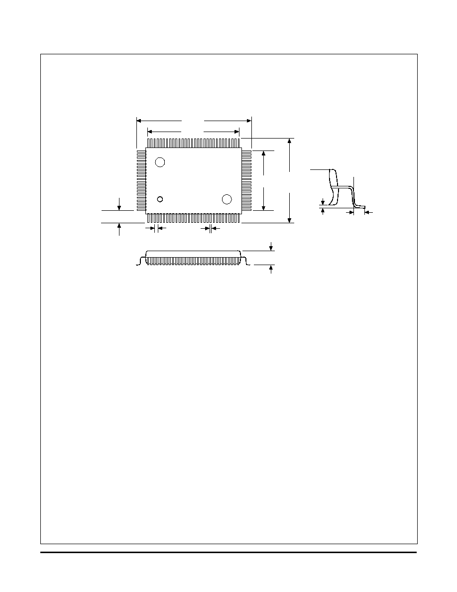
STEL-2060C
Package: 100-pin HQFP
Thermal coefficient,
ja
= 30
∞
C/W
PIN CONFIGURATION
Notes:
(1) Tolerances on pin spacing are not cumulative
(2) Dimensions shown are at seating plane
(3) I.C. denotes Internal Connection. This pin must be left unconnected. Do not use for vias.
(4) N.C. denotes No Connection. These pins can be used for vias.
21 V
SS
22 N.C.
23 PNCG1
24 PNCG2
25 DSCRAM
26 SYNC
27 LDG2
28 N.C.
29 N.C.
30 V
DD
31 V
DD
32 COUNT
0
33 COUNT
1
34 COUNT
2
35 COUNT
3
36 COUNT
4
37 COUNT
5
38 COUNT
6
39 COUNT
7
40 V
DD
41 V
SS
42 V
DD
43 PARL
44 READ
45 V
SS
46 ADDR
2
47 ADDR
1
48 ADDR
0
49 WRITE
50 CSEL
51 V
DD
52 V
DD
53 N.C.
54 DATA
7
55 DATA
6
56 DATA
5
57 DATA
4
58 DATA
3
59 DATA
2
60 DATA
1
61 DATA
0
62 N.C.
63 INT
64 N.C.
65 V
SS
66 ODCLK
67 N.C.
68 V
SS
69 DATO
70 N.C.
71 OOS
72 AUTO
73 N.C.
74 I.C.
75 N.C.
76 BERR
77 G1ERR
78 G2ERR
79 V
DD
80 V
DD
81 THR
0
82 THR
1
83 THR
2
84 THR
3
85 THR
4
86 THR
5
87 THR
6
88 THR
7
89 EXTSEL
90 V
SS
91 V
SS
92 V
SS
93 V
DD
94 V
SS
95 DDIF
96 V
SS
97 RATE
2
98 RATE
1
99 RATE
0
100 V
DD
PIN CONNECTIONS
1
V
DD
2
N.C.
3
N.C.
4
G1
0
5
G1
1
6
G1
2
7
G2
0
8
G2
1
9
G2
2
10 N.C.
11 OBIN
12 N.C.
13 V
SS
14 SYMCKIN
15 N.C.
16 V
SS
17 DCLKIN
18 N.C.
19 V
SS
20 RESET
Top View
0.941"
±
0.010"
0.742"
±
0.005"
0.487"
±
0.003"
0.705"
±
0.010"
0.11" nom.
0.122" max.
0.014"
±
0.002"
0.0256"
±
0.002"
0.031"
±
0.005"
0.009"
±
0.005"
Pin 1 Identifier
1
80
50
30
81
51
31
100
Detail of pins

STEL-2060C
4
INPUT SIGNALS
RESET
Reset
. A logic low on this asynchronous input will completely
reset all registers in the decoder to an initial condition within
20 nsec. Normal operation will commence after RESET goes
high. This will not affect the values stored in the decision
path memory but will reset the node sync state to the initial
condition.
DCLKIN
D
ecoder clock input. It is the reference clock for all internal
synchronous functions in the decoder when operating in the
Internal Puncturing mode. It should nominally be a square
wave with a maximum frequency of 45 MHz, corresponding
to a decoded data rate of 45 Mbps. When operating at Rate
1
/
2
and in the External Puncturing mode this clock will be
generated internally from SYMCKIN, and DCLKIN should
be connected to ground.
SYMCKIN
Sym
bol clock input. This is the reference clock for all
internal synchronous functions in the symbol alignment and
depuncturing circuits. It should nominally be a square wave
with a maximum frequency of 90 MHz. Its frequency should
be equal to f
DCLKIN
/2R in the parallel input mode
(PARL = 1) and equal to f
DCLKIN
/R in the sequential input
mode (PARL = 0), where R is the decoding rate when using
internal depuncturing. Please refer to the section on
Punctured Mode Operation for more detailed information.
G1
2-0
, G2
2-0
The G1
2-0
and G2
2-0
signals are the 3-bit soft decision input
symbols to the decoder. They are presented to the decoder
either sequentially or in parallel depending on the states of
the PARL and RATE
2-0
inputs. In the parallel mode
(PARL = 1) the symbols are clocked into the device on the
rising edges of SYMCKIN when RATE
2-0
= 0 (Rate
1
/
2
and
External Depuncturing) and on both edges of SYMCKIN
when RATE
2-0
0 (Internal Depuncturing). In the sequential
mode (PARL = 0) in which the
G2
2-0
inputs are not used, both
the G1 and G2 symbols are loaded via the G1
2-0
pins. The G1
symbols are then latched in on the rising edges of SYMCKIN
when LDG2 is low and the G2 symbols are latched in on the
rising edges of SYMCKIN when LDG2 is high.
LDG2
When this signal is high during a rising edge of SYMCKIN
the symbol loaded into the G1
2-0
pins will be G2. This
function is only active when PARL is set low (sequential
input mode) and RATE
2-0
is set to 000 (Rate
1
/
2
operation or
External Puncturing mode). If auto node sync is used, the
LDG2
signal can be derived by dividing the SYMCKIN
signal by two. The auto node sync will then compensate for
the phase ambiguity.
PARL
When this signal is high, the input symbols are accepted in
par
allel by the chip, using the G1
2-0
pins for the G1 symbols
and the G2
2-0
pins for the G2 symbols. When it is set low, the
inputs are accepted sequentially, using the G1
2-0
pins for
both symbols. The sequential input is most suited for BPSK
data, and the parallel input is most suited for QPSK data. The
auto node sync sequence will operate on the assumption that
the signal is BPSK modulated when PARL is set low and
QPSK modulated when it is set high. Setting PARL low adds
two cycles of ODCLK to the pipeline delay.
OBIN
The STEL-2060CCC can accept the soft-decision input data
in either offset binary or offset signed-magnitude formats.
When the OBIN input is set high, the format expected will be
offset binary; when it is set low it will be offset signed-
magnitude. The meanings of the 3-bit values for these two
codes is shown in the following table:
OBIN
= 1
OBIN
= 0
Value
111
111
Most confident +
110
110
(Data = 1)
101
101
100
100
Least confident +
011
000
Least confident ≠
010
001
001
010
(Data = 0)
000
011
Most confident ≠
When using the STEL-2060CCC with hard-decision data, the
symbols should be loaded into the G1
2
and G2
2
pins. The
other symbol inputs should be set to a logic high level and
OBIN
should be set low.
RATE
2-0
These signals select the decoding rate for unpunctured
operation (Rate
1
/
2
) and internally supported depuncturing
patterns (Rates
2
/
3
,
3
/
4
and
7
/
8
). These patterns are shown
in the following table, where a 0 in the pattern indicates a
punctured symbol:
RATE
2-0
Rate
Pattern
0 0 0
1
/
2
N.A.
0 0 1
2
/
3
G1: 10
G2: 11
1 0 0
3
/
4
G1: 101
G2: 110
0 1 0
7
/
8
G1: 1000101
G2: 1111010
Other puncturing patterns can be implemented externally
using the PNCG1 and PNCG2 inputs.
DDIF
When this input is set high, it causes the data out of the
Viterbi decoder to be differentially decoded. This adds one
cycle of ODCLK to the pipeline delay.

5
STEL-2060C
DSCRAM
When this input is set high, it causes the G2 symbols to be
inverted before they enter the Viterbi decoder, thereby
reversing the effect of the G2 inversion if an "Invert G2"
scrambler is implemented at the encoder.
PNCG1, PNCG2
The PNCG1 and PNCG2 signals are used to control the
STEL-2060CCC when operating in punctured modes not
supported by the internal puncturing logic. In normal
operation (Rate
1
/
2
and when using internal puncturing)
these pins should be set low. In the external depuncturing
mode, the PNCG1 signal must be set high to indicate that the
G1 symbol is punctured and the PNCG2 signal must be set
high to indicate that the G2 symbol is punctured. A symbol
will be depunctured when the PNCG1 or PNCG2 signals are
high during the rising edge of SYMCKIN which latches the
corresponding symbol in to the decoder. RATE
2-0
should be
set to 000 when operating in external depuncturing mode.
Zero value metrics will be substituted internally for the
actual metrics corresponding to the signals present on the
G1
2-0
and G2
2-0
pins at that time. Internal depuncturing can
be selected by the use of the RATE inputs.
SYNC
When the SYNC input is set high during the rising edge of
SYMCKIN
the internal symbol synchronization will be
changed. When auto node sync is not desired this pin should
be set low. It should be connected to the AUTO output to use
the auto node sync capability of the STEL-2060CCC. The
state of this circuit will always be set to normal after a reset.
COUNT
7-0
The 8-bit COUNT
7-0
input defines the period (number of
bits) used in the node synchronization circuit when EXTSEL
is set high. The 8-bit number N is used to set up a period of
(256N + 256) bits internally, where N is the value of
COUNT
7-0
. An out-of-sync condition is declared (i.e., the
output pin OOS is set high and AUTO pulses high) if the
renormalization count exceeds the threshold value during a
period of this number of bits.
THR
7-0
The 8-bit THR
7-0
input defines the threshold for node
synchronization when EXTSEL is set high. The 8-bit number
N is used to set up a threshold value of (8N + 6) internally,
where N is the value of THR
7-0
. An out-of-sync condition is
declared (i.e., the output pin OOS is set high and AUTO
pulses high) if the renormalization count exceeds this
threshold value.
EXTSEL
When the EXTSEL input is set high, the COUNT
7-0
and
THR
7-0
information is derived from the COUNT
7-0
and
THR
7-0
input pins. When it is set low, this information is
derived from the data written into addresses 0 and 1.
OUTPUT SIGNALS
ODCLK
O
utput data clock. All outputs change on the rising edge of
this clock. The falling edge of ODCLK can be used as a strobe
for DATO output, which is guaranteed to be valid on this
edge.
DATO
Decoded data output. This is the output of the Viterbi
decoder. This signal changes on the rising edges of ODCLK.
In Rate
1
/
2
operation there will be a pipeline delay of 526
cycles of ODCLK from the G1
2-0
/G2
2-0
inputs to the DATO
output when DDIF is set low and PARL is set high. Setting
DDIF
high adds one cycle to this value and setting PARL low
adds two cycles.
OOS
This output pin serves as a flag for the out-of-sync condition.
When it goes high it signifies that the renormalization count
in the internal node sync circuit has exceeded the threshold
value set by the THR
7-0
signal, declaring an out-of-sync
condition. It will remain high until this condition ceases to
exist. i.e., until the next time the threshold is not exceeded
during a complete count period.
AUTO
This is the feedback signal from the internal node sync
correction circuit. It will pulse high for one cycle of DCLKIN
each time the renormalization count in the internal node
sync circuit has exceeded the threshold value set by the
THR
7-0
signal and the out-of-sync condition is declared. It
should be connected to the SYNC input when using the
internal node sync facility.
BERR
The Bit Error output indicates that an error has been detected
in either the G1 or G2 symbols corresponding to the current
output bit.
G1ERR
The G1 Error output indicates that an error has been detected
in the G1 symbol corresponding to the current output bit.
G2ERR
The G2 Error output indicates that an error has been detected
in the G2 symbol corresponding to the current output bit.
Note
: The BERR, G1ERR and G2ERR signals are in NRZ
format, i.e., the signals will not return to zero between two
consecutive errors. To generate pulsed outputs, the signals
can be gated with the ODCLK signal.
MICROPROCESSOR INTERFACE
DATA
7-0
All I/O and control functions can be accessed via the
DATA
7-0
bus with the associated control signals. The
STEL-2060CCC is used as a memory or I/O mapped
peripheral to the host processor.

STEL-2060C
6
ADDR
2-0
The 3-bit address bus is used to access the various I/O
functions, as shown in the Memory Map table, below. Note
that some addresses contain both Read and Write registers.
These read and write mode registers are separate and contain
different data.
WRITE
The Write input is used to write data to the microprocessor
data bus. It is active low and is normally connected to the
write line of the host processor.
READ
The Read input is used to read data from the microprocessor
data bus. It is active low and is normally connected to the
read line of the host processor.
CSEL
The Chip Select input can be used to selectively enable the
microprocessor data bus. It is active low.
INT
The Interrupt output indicates when the Period Counter in
the BER Monitor has completed a count period, and that a
new value of BERCT is ready to be read from addresses 0
H
and 1
H
, when INT will go high for one symbol period.
INPUT (WRITE) FUNCTIONS
COUNT
7-0
The 8-bit COUNT
7-0
data defines the period (i.e., the number
of bits) used in the node synchronization circuit. The 8-bit
number N is used to set up a period of (256N + 256) internally,
where N is the value of COUNT
7-0
. If the renormalization
count exceeds the threshold value during a period of this
number of bits then an out-of-sync condition is declared (i.e.,
the output pin OOS is set high and AUTO pulses high).
Reset value 00
H
.
THR
7-0
The 8-bit THR
7-0
data defines the threshold for node
synchronization when EXTSEL is set low. The function is
identical to that of the THR
7-0
input signal. Reset value 00
H
.
BPER
23-0
The 24-bit BER Period data is used to set the period (number
of data bits) over which the mean BER is measured by the
BER Monitor. The period used is 1000 times the value of
BPER
23-0
. Reset value FFFFFF
H
.
Note:
The BER Count function incorporated in the
STEL-2060CCC uses a counter to count the number of
thousands of bits received. When the value of this counter is
equal
to the value written into BPER
23-0
the number of errors
counted is dumped into the BERCT
15-0
output register and
can be read from read addresses 0-1
H
. Simultaneously, both
the error and bit counters are reset and the process is restarted,
and an interrupt (INT) is generated to indicate that the new
value is ready to be read.
Since the default (reset) value of the BPER
23-0
register is
FF FF FF
H
a potential problem occurs if the desired value is
not written into this register before the value of the counter
has already incremented past this value. If this is not done
the equality will not be detected until after the counter
overflows and increments to the desired value once again.
Even at the maximum rate of 45 Mbps this will take over 6
minutes and, at a more modest data rate, such as 1 Mbps, it
will take over 4
1
/
2
hours! In any case, the user can easily be
misled into believing that the circuit is not operating correctly
since the interrupts will not be generated as expected. It is
therefore imperative that the BPER
23-0
value be written into
the STEL-2060CCC as soon as possible after a reset to ensure
that this condition does not take place. The maximum time
allowable is just less than the desired interrupt period itself,
since the counter begins counting right after the reset is
released.
e.g., if the desired interrupt period is one second, the
BPER
23-0
value must be written within one second of the
reset. At a data rate of 1 Mbps the period would correspond
to 10
6
bits and the correct BPER
23-0
value would be 10
3
, or
00 03 E8
H
.
If, for some reason, it is not possible to do this, a dummy
value should first be written into the STEL-2060CCC. This
should be large enough so that, at the time of writing, the bit
counter will not have exceeded the dummy value. In this
way the first interrupt will be generated within a reasonable
period of time and the dummy value can then be overwritten
with the desired value. Again, care must be taken to ensure
that the BPER
23-0
value written is greater than the
instantaneous counter value, otherwise the same problem
will occur.
e.g., in the above example, if it is not possible to write the
BPER
23-0
value until 5 seconds after the reset, then a dummy
BPER
23-0
value corresponding to >5 seconds, e.g., 6 seconds,
or 00 17 70
H
should first be written. The desired value of
00 03 E8
H
must then be written within one second of an
interrupt generated by the STEL-2060CCC, thereby ensuring
that the counter has not exceeded the new value at that time.
OUTPUT (READ) FUNCTIONS
BERCT
15-0
The 16-bit Bit Error Count data represents the mean Bit Error
Rate over the period determined by the BER Period data
BPER
23-0
. The actual BER is given by:
8 x BERCT
15-0
BER =
1000 x BPER
23-0
The value will be updated each time the period counter
completes its count. Completion is indicated by the INT
output going high for one clock cycle. If the accumulator
overflows during a measurement period its output will be
caused to saturate at a value of FFFF
H
.

7
STEL-2060C
MICROPROCESSOR INTERFACE MEMORY MAP
WRITE MODE REGISTERS
ADDR
2-0
DATA
7
DATA
6
DATA
5
DATA
4
DATA
3
DATA
2
DATA
1
DATA
0
0
COUNT
7
COUNT
6
COUNT
5
COUNT
4
COUNT
3
COUNT
2
COUNT
1
COUNT
0
1
THR
7
THR
6
THR
5
THR
4
THR
3
THR
2
THR
1
THR
0
2
3
BPER
7
BPER
6
BPER
5
BPER
4
BPER
3
BPER
2
BPER
1
BPER
0
4
BPER
15
BPER
14
BPER
13
BPER
12
BPER
11
BPER
10
BPER
9
BPER
8
5
BPER
23
BPER
22
BPER
21
BPER
20
BPER
19
BPER
18
BPER
17
BPER
16
READ MODE REGISTERS
ADDR
2-0
DATA
7
DATA
6
DATA
5
DATA
4
DATA
3
DATA
2
DATA
1
DATA
0
0
BERCT
7
BERCT
6
BERCT
5
BERCT
4
BERCT
3
BERCT
2
BERCT
1
BERCT
0
1
BERCT
15
BERCT
14
BERCT
13
BERCT
12
BERCT
11
BERCT
10
BERCT
9
BERCT
8
PUNCTURED MODE OPERATION
CONCEPT OF PUNCTURING
In punctured codes some of the symbols generated by the
convolutional encoder are deleted, or punctured, from the
transmitted sequence. For example, in a rate
1
/
2
(unpunctured) sequence, four symbols are transmitted for
every two data bits. If one symbol out of every group of
four was punctured from the sequence then only three
symbols would be transmitted for every two data bits. This
would result in a rate
2
/
3
code. The coding gain is
significantly less than that for unpunctured operation, but
this is the trade-off for the reduced bandwidth required to
transmit the information. The STEL-2060CC decoder is
designed to operate with punctured codes as well as rate
1
/
2
code. Two methods are provided for depuncturing the
symbols. The external method can be used for all rates and
patterns up to rate
7
/
8
by indicating which symbols were
punctured at the encoder (and then reinserted prior to
decoding) with the PNCG1 and PNCG2 signals. When one
of these signals is set high the input data at the corresponding
symbol input is ignored, and the internally generated metric
for the symbol pair (G1 and G2) assigns a zero weight to the
punctured symbol in the pair. This is done because the
Viterbi decoder has no way of knowing what the punctured
symbol should have been. The recommended puncturing
sequences for the various
(N-1)
/
N
rates of punctured
operation are shown in the tables. The portions shown in
boldface are the basic sequences, which are then repeated.
The use of the PNCG1 and PNCG2 signals for rate
3
/
4
is
shown in the External Puncturing timing diagrams. The
sequence for rate
3
/
4
is G1 G2 P G2 G1 P, and the punctured
symbols are marked with asterisks in the timing diagrams.
USING INTERNAL DEPUNCTURING
The internal depuncturing method supports Rates
2
/
3
,
3
/
4
and
7
/
8
using the puncturing sequences specified in the
tables, and the node sync process will automatically find the
correct places to reinsert the punctured symbols. The
puncturing sequences used for the rates supported are shown
in the tables, along with the speeds of the two input clocks,
SYMCKIN
and DCLKIN. The portions shown in boldface
are the basic sequences, which are then repeated. The
symbol sequence for rate
2
/
3
is shown in the Internal
Puncturing timing diagrams. The sequence is G1 G2 P G2;
only G1 symbols are punctured in this particular sequence.
The SYMCKIN and DCLKIN clocks are used to clock in the
symbols and to clock out the data bits. The speeds of these
two clocks vary according to the modes and rate in use.
When operating in the External Depuncturing modes the
DCLKIN
signal is not used and the SYMCKIN speed will be
equal to the data rate (D) in the parallel mode (PARL = 1) and
be equal to twice the data rate (2D) in the sequential mode
(PARL = 0). In the Internal Depuncturing modes, however,
DCLKIN
is used and the speed of SYMCKIN will be as
shown in the tables.
The depuncturing circuit in the STEL-2060CC takes symbols
synchronized to the SYMCKIN signal and depunctures them,
i.e., inserts dummy symbols into the signal stream at the
appropriate positions. To do this the circuit handles the
symbols as a group of up to four pairs, depending on the code
rate. This circuit operates at the SYMCKIN rate and, at this
point, the group of depunctured symbols is transferred into
another set of registers clocked with DCLKIN. There is an
internal timing requirement that the falling edge of DCLKIN
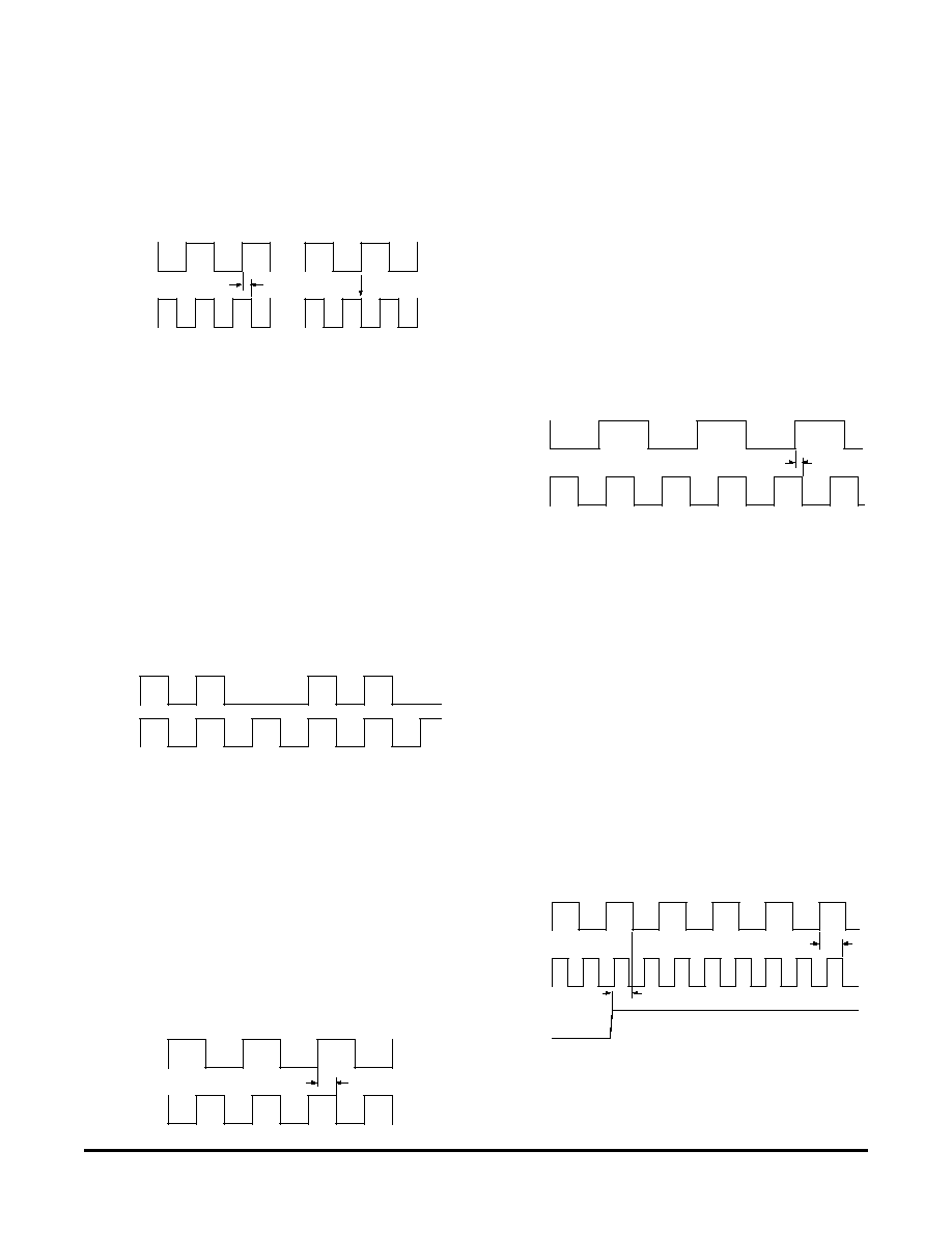
STEL-2060C
8
must follow the rising edge of SYMCKIN by a minimum of
8 nsec. at this instant, otherwise the handover will not occur
correctly. This occurs once every 4 cycles of DCLKIN at rate
7
/
8
, every 2 cycles at rate
3
/
4
and every 3 cycles at rate
2
/
3
, the
number of cycles of SYMCKIN depending on whether the
parallel or sequential input mode is used, as well as the code
rate. Two examples of clock phasing for rate
3
/
4
parallel
operation are shown below.
Here, the timing is such that the falling edges of DCLKIN
only coincide with falling edges of SYMCKIN, never with
rising edges. In this case the timing violation never occurs at
any speed, since the non-coincident falling edges of DCLKIN
will trail the rising edges of SYMCKIN by approximately 8
nsec. at a speed of 45 Mbps. Again, the same caveat regarding
jitter must be observed. However, the symbol signal setup
and hold requirements, shown in page 11 of the data sheet
make it necessary for SYMCKIN to have a minimum low
time of 12 nsec. to satisfy these requirements, so that it is not
possible for this signal to be a square wave above 40 MHz for
this reason. Since the method for eliminating the clock
timing violation presented here relies on the use of square
waves (50% mark-space ratio), it cannot be used above 40
MHz because of the setup and hold time requirements.
Again, a similar condition exists for rate
7
/
8
operation, as
shown below.
SYMCKIN
DCLKIN
Good
Bad
In the first example the falling edges of DCLKIN never
coincide with the rising edges of SYMCKIN. Thus the timing
violation will never occur provided that the delay from the
non-coincident rising edges of SYMCKIN to the following
falling edge of DCLKIN (shown by the arrows) exceeds 8
nsec. In the second case the falling edge of DCLKIN coincides
with the rising edge of SYMCKIN once every two cycles of
DCLKIN, resulting in a 50% probability that this may be the
point at which the handover occurs, creating the problem
discussed above.
There are several ways to satisfy the timing requirement,
depending on the code rate. One effective way which works
at all rates is to generate SYMCKIN from DCLKIN by
puncturing the clock to reduce its frequency while keeping
all the edges synchronized; this will require the use of a small
FIFO to buffer the input symbols to cope with the punctured
clock. The rate
3
/
4
timing is shown below as an example.
SYMCKIN
DCLKIN
For rate
3
/
4
operation it is possible to generate the two clocks
with a mutual phase relationship that can exclude the timing
violation, as was shown in the first figure. As previously
stated, provided the two clocks can be generated as shown in
the first example, where only the rising edges of DCLKIN
coincide with the edges of SYMCKIN, the timing violation
will never occur provided that the delay from the non-
coincident rising edges of SYMCKIN to the following falling
edge of DCLKIN (shown by the arrows) exceeds 8 nsec. In
the example shown this will be true at data rates up to 30
Mbps. Care must be taken to ensure that jitter between the
clocks is kept low enough to avoid the timing violation
condition. A similar condition exists for rate
2
/
3
operation,
as shown below.
SYMCKIN
DCLKIN
SYMCKIN
DCLKIN
However, in this case the timing violation will begin to occur
at speeds over 15 Mbps, so that this method of solving the
timing problem is less useful for rate
7
/
8
operation.
Note that for sequential mode operation (PARL = 0) the
frequency of the SYMCKIN signal will be doubled in every
case. This presents a problem with the synchronized clock
method presented here since it will not be possible to generate
the necessary waveforms with the correct mutual phasing
guaranteed because of the phase ambiguity of the SYMCKIN
signal itself relative to the internal handover process. In this
case it will be necessary to use either the punctured clock
approach or the synchronized reset approach.
The third method, which, while having the disadvantage
that it is susceptible to loss of sync from disturbances, is
easier to implement than clock puncturing and provides a lot
more margin than simple clock phase synchronization. It
consists of a synchronized reset generator used in conjunction
with clock phase synchronization. This is shown below for
rate
7
/
8
.
RESET
SYMCKIN
DCLKIN
15 nsec. min.
This ensures that the STEL-2060CC starts up during the
optimum phase of the SYMCKIN/DCLKIN repetition cycle,
i.e., the phase with the maximum separation between the
rising edge of SYMCKIN and the next falling edge of DCLKIN;

9
STEL-2060C
the decoder will then continue to operate correctly provided
that nothing occurs to upset this cycle. This method exploits
the fact that not all falling edges of DCLKIN have a timing
sensitivity relative to the rising edges of SYMCKIN, as was
discussed earlier. For example, in rate
7
/
8
operation only
every fourth falling edge of DCLKIN is critical, starting with
the fourth one after the reset is released. By timing the rising
edge of the reset at a point in the cycle where there is good
separation between the rising edge of SYMCKIN and the
following falling edge of DCLKIN the same situation will
occur again every four cycles of DCLKIN, which is precisely
where the timing sensitivity occurs, as shown in the figure.
This method ensures good timing margins for stable operation
at all data rates up to 40 Mbps, this limit again being set by
the symbol setup and hold time requirements and need to
use square waves for the clocks.
ELECTRICAL CHARACTERISTICS
ABSOLUTE MAXIMUM RATINGS
Warning:
Stresses greater than those shown below may cause permanent damage to the
device. Exposure of the device to these conditions for extended periods may also affect device
reliability.
Symbol
Parameter
Range
Units
T
stg
Storage Temperature
≠65 to +150
∞
C
T
a
Operating Temperature (Ambient)
≠40 to +85
∞
C
V
DDmax
Max. voltage between V
DD
and V
SS
+7 to ≠0.7
volts
V
I/O(max)
Max. voltage on any input or output pin
V
DD
+ 0.3
volts
V
I/O(min)
Min. voltage on any input or output pin
V
SS
≠ 0.3
volts
RECOMMENDED OPERATING CONDITIONS
Symbol
Parameter
Range
Units
V
DD
Supply Voltage
+5
±
10%
volts
T
a
Operating Temperature (Ambient)
0 to +70
∞
C
D.C. CHARACTERISTICS
(Operating Conditions: V
DD
= 5.0
±
5% volts, T
a
= 0
∞
to 70
∞
C)
Symbol
Parameter
Min. Typ. Max.
Units
Conditions
I
DD(Q)
Supply Current, Quiescent
1.0
mA
Static, no clock
I
DD
Supply Current, Operational
8
mA/Mbps
@ 45 Mbps (f
DATA
)
V
IH(min)
Min. High Level Input Voltage
2.0
volts
Guaranteed Logic '1'
V
IL(max)
Max. Low Level Input Voltage
0.8
volts
Guaranteed Logic '0'
V
OH(min)
Min. High Level Output Voltage
2.4
volts
I
O
= ≠4.0 mA
V
OL(max)
Max. Low Level Output Voltage
0.4
volts
I
O
= +4.0 mA
I
IH(max)
Max. High Level Input Current
10
µ
A
V
IN
= +5.0 volts
I
IL(max)
Max. Low Level Input Current
≠10
µ
A
V
IN
= 0 volts
STEL-2060C
10
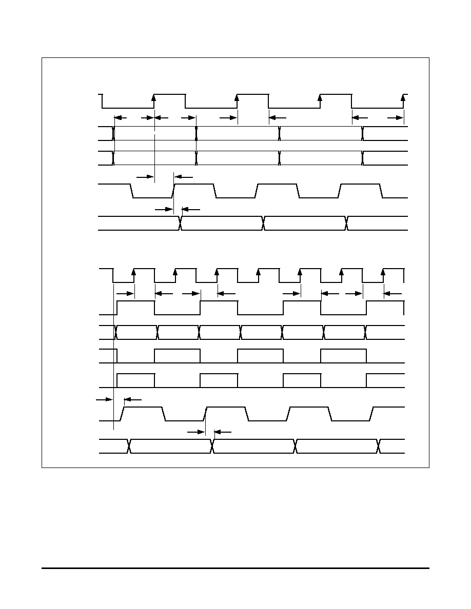
(a) PARALLEL INPUT MODE (PARL = 1)
TIMING. RATE
1
/
2
AND EXTERNAL DEPUNCTURING
(b) SEQUENTIAL INPUT MODE (PARL = 0)
G1/2
G1
G2
G2
DATO
LDG2
PNCG2
G1
G2
G1
G2
G1
ODCLK
SYMCKIN
PNCG1
t
SU
t
HD
t
SHS
t
SO
t
OD
t
SLS
G1/2
PNCG1/G2
SYMCKIN
SYMB. N
DATO
ODCLK
SYMB. N+1
SYMB. N+2
t
SHPE
t
SU
t
HD
t
SO
t
OD
t
SLPE

11
STEL-2060C
A.C. CHARACTERISTICS
(Operating Conditions: V
DD
= 5.0
±
5% volts, T
a
= 0
∞
to 70
∞
C)
Symbol
Parameter
Min.
Max.
Units
Conditions
f
DAT
Data speed, Parallel input mode (PARL = 1),
45
Mbps
PARL
= 1 and
all rates when not using Internal Depuncturing
RATE
2-0
= 0
f
DAT
Data speed, Sequential input mode (PARL = 0), Rate
1
/
2
45
Mbps
PARL
= 0 or
and all rates and modes when using Internal Depuncturing
RATE
2-0
0
t
SU
G1
, G2, PNCG1 or PCNG2, LDG2 to SYMCKIN Setup
3
nsecs.
PARL
= 0 or
t
HD
G1
, G2, PNCG1 or PCNG2, LDG2 to SYMCKIN Hold
5
nsecs.
RATE
2-0
= 0
t
SUI
G1
, G2, PNCG1 or PCNG2, LDG2 to SYMCKIN Setup
6
nsecs.
PARL
= 1 and
t
HDI
G1
, G2, PNCG1 or PCNG2, LDG2 to SYMCKIN Hold
6
nsecs.
RATE
2-0
0
t
SHPE,
t
SLPE
SYMCKIN
Pulse width (high or low), Parallel input mode,
10
nsecs.
PARL
= 1 and
all rates when not using Internal Depuncturing
RATE
2-0
= 0
t
SHPI,
t
SLPI
SYMCKIN
Pulse width (high or low), Parallel input mode,
12
nsecs.
PARL
= 1 and
all rates when using Internal Depuncturing
RATE
2-0
0
t
SHS,
t
SLS
SYMCKIN
Pulse width (high or low), Serial input mode
6
nsecs.
PARL
= 0
t
SO
SYMCKIN
to ODCLK stable delay (RATE
2-0
= 000)
3
8
nsecs.
t
DO
DCLKIN
to ODCLK stable delay (RATE
2-0
000)
3
8
nsecs.
Load = 15 pF
t
OD
ODCLK
to output stable delay, all other outputs
1
3
nsecs.
Load = 15 pF
}
}
}
}
}
}

STEL-2060C
12
PUNCTURED SYMBOL SEQUENCES
1. RATE
1
/
2
AND EXTERNAL DEPUNCTURING - SEQUENTIAL INPUTS (PARL = 0)
Rate
Symbol sequence (suffix is symbol number in sequence, all at G1
2-0
input)
SYMCKIN DCLKIN
1
/
2
G1
1
G2
1
G1
2
G2
2
G1
3
G2
3
(Not Punctured)
2 D
0
2
/
3
G1
1
G2
1
P
2
G2
2
G1
3
G2
3
P
4
G2
4
G1
5
G2
5
P
6
G2
6
2 D
0
3
/
4
G1
1
G2
1
P
2
G2
2
G1
3
P
3
G1
4
G2
4
P
5
G2
5
G1
6
P
6
G1
7
G2
7
2 D
0
4
/
5
G1
1
G2
1
P
2
G2
2
P
3
G2
3
P
4
G2
4
G1
5
G2
5
P
6
P
6
G2
7
P
7
2 D
0
5
/
6
G1
1
G2
1
P
2
G2
2
G1
3
P
3
P
4
G2
4
G1
5
P
5
G1
6
G2
6
P
7
G2
7
2 D
0
6
/
7
G1
1
G2
1
P
2
G2
2
P
3
G2
3
G1
4
P
4
P
5
G2
5
G1
6
P
6
G1
7
G2
7
2 D
0
7
/
8
G1
1
G2
1
P
2
G2
2
P
3
G2
3
P
4
G2
4
G1
5
P
5
P
6
G2
6
G1
7
P
7
2 D
0
2. RATE
1
/
2
AND EXTERNAL DEPUNCTURING - PARALLEL INPUTS (PARL = 1)
Rate
Input
Symbol sequence (suffix is symbol number in sequence)
SYMCKIN DCLKIN
1
/
2
G1
2-0
G1
1
G1
2
G1
3
G1
4
G1
5
G1
6
(Not Punctured)
D
0
G2
2-0
G2
1
G2
2
G2
3
G2
4
G2
5
G2
6
2
/
3
G1
2-0
G1
1
P
2
G1
3
P
4
G1
5
P
6
G1
7
P
8
G1
9
P
10
D
0
G2
2-0
G2
1
G2
2
G2
3
G2
4
G2
5
G2
6
G2
7
G2
8
G2
9
G2
10
3
/
4
G1
2-0
G1
1
P
2
G1
3
G1
4
P
5
G1
6
G1
7
P
8
G1
9
G1
10
D
0
G2
2-0
G2
1
G2
2
P
3
G2
4
G2
5
P
6
G2
7
G2
8
P
9
G2
10
4
/
5
G1
2-0
G1
1
P
2
P
3
P
4
G1
5
P
6
P
7
P
8
G1
9
P
10
D
0
G2
2-0
G2
1
G2
2
G2
3
G2
4
G2
5
G2
6
G2
7
G2
8
G2
9
G2
10
5
/
6
G1
2-0
G1
1
P
2
G1
3
P
4
G1
5
G1
6
P
7
G1
8
P
9
G1
10
D
0
G2
2-0
G2
1
G2
2
P
3
G2
4
P
5
G2
6
G2
7
P
8
G2
9
P
10
6
/
7
G1
2-0
G1
1
P
2
P
3
G1
4
P
5
G1
6
G1
7
P
8
P
9
G1
10
D
0
G2
2-0
G2
1
G2
2
G2
3
P
4
G2
5
P
6
G1
7
G2
8
P
9
G2
10
7
/
8
G1
2-0
G1
1
P
2
P
3
P
4
G1
5
P
6
G1
7
G1
8
P
9
P
10
D
0
G2
2-0
G2
1
G2
2
G2
3
G2
4
P
5
G2
6
P
7
G2
8
G2
9
G2
10
3. INTERNAL DEPUNCTURING - SEQUENTIAL INPUTS (PARL = 0)
Rate
Symbol sequence (suffix is symbol number in sequence, all at G1
2-0
input)
SYMCKIN DCLKIN
1
/
2
G1
1
G2
1
G1
2
G2
2
G1
3
G2
3
G1
4
G2
4
G1
5
(Not Punctured)
2 D
0
2
/
3
G1
1
G2
1
G2
2
G1
3
G2
3
G2
4
G1
5
G2
5
G2
6
G1
7
G2
7
G2
8
3
/
2
D
D
3
/
4
G1
1
G2
1
G2
2
G1
3
G1
4
G2
4
G2
5
G1
6
G1
7
G2
7
G2
8
G1
9
4
/
3
D
D
7
/
8
G1
1
G2
1
G2
2
G2
3
G2
4
G1
5
G2
6
G1
7
G1
8
G2
8
G2
9
G2
10
8
/
7
D
D
4. INTERNAL DEPUNCTURING - PARALLEL INPUTS (PARL = 1)
Rate
Input
Symbol sequence (suffix is symbol number in sequence)
SYMCKIN DCLKIN
1
/
2
G1
2-0
G1
1
G1
2
G1
3
G1
4
G1
5
G1
6
G1
7
(Not Punctured)
D
0
G2
2-0
G2
1
G2
2
G2
3
G2
4
G2
5
G2
6
G2
7
2
/
3
G1
2-0
G1
1
G2
2
G2
3
G1
5
G2
6
G2
7
G1
9
G2
10
G2
11
3
/
4
D
D
G2
2-0
G2
1
G1
3
G2
4
G2
5
G1
7
G2
8
G2
9
G1
11
G2
12
3
/
4
G1
2-0
G1
1
G2
2
G1
4
G2
5
G1
7
G2
8
G1
10
G2
11
G1
13
G2
14
2
/
3
D
D
G2
2-0
G2
1
G1
3
G2
4
G1
6
G2
7
G1
9
G2
10
G1
12
G2
13
G1
15
7
/
8
G1
2-0
G1
1
G2
2
G2
4
G2
6
G1
8
G2
9
G2
11
G1
13
G1
15
G2
16
4
/
7
D
D
G2
2-0
G2
1
G2
3
G1
5
G1
7
G2
8
G2
10
G1
12
G2
14
G2
15
G1
17

13
STEL-2060C
G1 N
G1
DATO
DCLKIN
ODCLK
SYMCKIN
*
G2 N+1
**
G2 N+2
G2 N
G2
G1 N+2
G2 N+3
***
G1 N+4
G2 N+4
**
G1 N+1 Punctured
***
G1 N+3 Punctured
Basic Pattern
t
DO
t
OD
t
SUI
t
HDI
*
Within each symbol period, rising edge of SYMCLKIN must precede falling edge, as shown
t
SHPI
t
SLPI
(a) PARALLEL INPUT MODE (PARL = 1)
INTERNAL DEPUNCTURING TIMING. RATE
2
/
3
SHOWN
(b) SEQUENTIAL INPUT MODE (PARL = 0)
t
OD
G1/2
G1 N
G2 N
G2 N+4
G2 N+1
**
G1 N+2
G2 N+2
G2 N+3
***
G1 N+4
SYMCKIN
DATO
DCLKIN
ODCLK
**
G1 N+1 Punctured
***
G1 N+3 Punctured
Basic Pattern
t
DO
t
SUI
t
HDI
t
SHS
t
SLS

STEL-2060C
14
G1/2
G2
G1
G2
G1
G2
G1
G2
G1
G2
G1
G2
G1
G2
G1
G2
PNCG1
PNCG2
*
*
*
*
*
SYMCKIN
DATO
ODCLK
LDG2
t
SU
t
HD
*
Indicates Punctured Symbols
(a) PARALLEL INPUT MODE (PARL = 1)
EXTERNAL DEPUNCTURING TIMING. RATE
3
/
4
SHOWN
G1
G2
PNCG1
PNCG2
*
*
*
*
*
SYMCKIN
DATO
ODCLK
*
Indicates Punctured Symbols
t
SU
t
HD
(b) SEQUENTIAL INPUT MODE (PARL = 0)
15
STEL-2060C
ADDR2-0
DATA 7-0
WRITE
CSEL
DON'T CARE
DON'T CARE
ADDR2-0
READ
CSEL
DATA 7-0
DON'T CARE
DON'T CARE
t
SM
t
HM
t
WW
t
HM
t
SM
t
ZV
t
VZ
1. WRITE MODE
2. READ MODE
A.C. CHARACTERISTICS
(Operating Conditions: V
DD
= 5.0
±
5% volts, T
a
= 0
∞
to 70
∞
C)
Symbol
Parameter
Min.
Max.
Units
t
SM
CSEL
, ADDR
2-0
or DATA
7-0
to WRITE or READ Setup
10
nsecs.
t
HM
CSEL
, ADDR
2-0
or DATA
7-0
to WRITE or READ Hold
5
nsecs.
t
WW
WRITE
Pulse width
5
nsecs.
t
ZV
READ
(low) to DATA
7-0
Valid
10
nsecs.
t
VZ
READ
(high) to DATA
7-0
High-Impedance
10
nsecs.
MICROPROCESSOR INTERFACE TIMING

STEL-2060C
16
NODE SYNCHRONIZATION
In a communication system using Viterbi decoding the de-
coder will only operate correctly when the symbols G1 and
G2 are loaded into the decoder in the correct order. Identi-
fying which symbol is G1 and which one is G2 is referred to
as node synchronization. The STEL-2060C contains a circuit
designed to carry out the node synchronization function
automatically. It uses the internally generated metrics of the
received sequence to do this. These constantly changing
parameters are periodically renormalized to keep them
within bounds. If renormalization occurs too frequently it is
a good indication that the system is not converging, most
likely due to lack of node synchronization. The renormal-
ization rate at which the system will decide to change the
node sync is determined by the threshold parameter. This is
an 8-bit number which is set by the THR
7-0
inputs. When the
renormalization count exceeds this value, the OOS output
will go high and the AUTO output will pulse high for one
clock cycle, as shown during Count Window N in the timing
diagram below. The counter is reset after a number of bits
determined by the number set by the COUNT
7-0
inputs, so
that the threshold must be exceeded somewhere in that
period for resynchronization to take place. OOS will be
reset if the counter then counts through an entire window
and the threshold is not exceeded, as shown during Count
Window N + 1 in the timing diagram below. The most
suitable threshold setting will depend on the value of
E
b
/N
0
, the coding rate, and the signal level at the G1 and G2
inputs. For full scale inputs, i.e., the peak signal values
almost saturate the digital inputs, suitable starting values
for the threshold will be 1% for Rate
1
/
2
, 0.5% for Rates
2
/
3
to
6
/
7
, and 0.1% for Rate
7
/
8
. e.g., for Rate
1
/
2
, if the number of
bits over which the measure is made is set to 512
(COUNT
7-0
= 01
H
) the threshold should be set to 5. Setting
THR
7-0
= 0 gives a value of 6, which is adequately close.
More reliable results will be obtained by counting over a
longer period to improve the averaging process, but this
increases the time taken to make a decision and hence to
acquire node sync. Thus, starting with a low count period
and then increasing it (and adjusting the threshold accord-
ingly to maintain a value of 1%) when OOS goes low will
result in a faster acquisition of correct node sync with a
lower probability of accidental loss of node sync once cor-
rect sync has been achieved. To use the internal node sync
the AUTO output must be connected to the SYNC input.
The synchronization sequence depends on the setting of the
PARL
input. When PARL is set low it is assumed that the
data was modulated using BPSK, and when it is set high it is
assumed that the data was modulated using QPSK. The
appropriate synchronization sequences will be invoked, as
shown in the node sync sequence tables. Note that the
pipeline delay through the device will be affected by the
node sync state. If multiple devices are used in parallel to
achieve higher data rates, it is necessary for the all devices to
have the same node sync state to equalize their pipeline
delays. It will be necessary to reset the devices together to
achieve this state
When internal depuncturing is used, additional node sync
states exist because of the uncertainty of the current symbol
position in the puncture sequence. In this case the node sync
circuit will also search through the sequence by adding
delays in the depuncturing process to precess through the
sequence. In the sequential input mode (PARL = 0) this is
simply an extension of the node sync process, since the
alternate state is achieved by delaying the symbols. In the
parallel input mode, however, this is different from the
"invert G2 and swap" process, and in this sync sequence
"invert G2 and swap" precedes the delay addition, so that
the system goes through both the initial and alternate states
for each delay addition tried. This is shown for the Rate
2
/
3
case. In each case the symbols are read into the depunc-
turing circuit in groups of three (in the BPSK mode) or six (in
the QPSK mode) and attempts are made to reinsert the
punctured symbol in all of the possible insertion positions.
The positions of the punctured symbols in the sequences are
shown by the asterisks (*). The resulting groups of four or
eight symbols are then decoded in pairs, resulting in two
decoded bits in the BPSK mode and four bits in the QPSK
mode. For higher rates the sequences will be extensions of
this procedure.
When external depuncturing is used, the determination of
which symbols were punctured, and need to be reinserted
into the symbol sequence, is part of the node sync process.
This is because the acquisition of correct node sync cannot be
completed until the punctured symbols are reinserted cor-
rectly. The AUTO and OOS outputs of the STEL-2060C can
be used as indicators of the operation of the internal node
sync process; OOS will remain high as long as node sync has
not been achieved and AUTO will pulse each time a new
node sync state is being tried. Since there are only two
possible internal node sync states, alternate pulses on the
AUTO
output can be used as an indication that the depunc-
turing is incorrect and a new depuncturing sequence should
be tried externally.
NODE SYNC TIMING
AUTO
OOS
ODCLK
Count Window N
Count Window N+1

17
STEL-2060C
Input
Initial State
Alternate States
1
2
G1
G1
n
G2
n
* G2
n+1
G2
n
* G2
n+1
G1
n+2
G2
n+1
G1
n+2
G2
n+2
*
(No delay)
(One symbol
(Two symbol
delay)
delay)
PARL
Input
Initial State
Alternate State
0
G1
G1
n
G2
n
G2
n
G1
n+1
G2
N.A.
N.A.
1
G1
G1
n
G2
n
G2
G2
n
G1
n
Input
Initial State
Alternate States
1
2
3
4
5
G1
G1
n
G2
n+1
G2
n+2
*
G2
n
* G1
n+2
G2
n+3
G2
n
* G1
n+2
G2
n+3
G2
n+1
G2
n+2
* G1
n+4
*G2
n+1
G2
n+2
*G1
n+4
G1
n+2
G2
n+3
G2
n+4
*
G2
G2
n
* G1
n+2
G2
n+3
G1
n
G2
n+1
G2
n+2
* G2
n+1
G2
n+2
* G1
n+4
G2
n
* G1
n+2
G2
n+3
G1
n+2
G2
n+3
G2
n+4
G2
n+1
G2
n+2
*G1
n+4
(No Invert/Swap (Invert/Swap
(No Invert/Swap
(Invert/Swap
(No Invert/Swap
(Invert/Swap
No delay)
No delay)
One symb. delay) One symb. delay) Two symb. delay)
Two symb. delay)
3. RATE
2
/
3
, PARL = 1 (QPSK MODE)
NODE SYNC SEQUENCES
1. RATE
1
/
2
2. RATE
2
/
3
, PARL = 0 (BPSK MODE)
BER PERFORMANCE
The coding gain obtained by the use of Convolutional coding
and Viterbi decoding is extremely dependent on many
parameters. Not surprisingly, the code rate is a primary
factor, but so are the bit error rate (BER) and amplitude of the
input signal. The BER affects the coding gain because the
error correction capability of the Viterbi decoder is
dependent on the statistics of the errors, specifically the
clustering of errors. As the BER of the input signal increases,
so does the clustering, causing a reduction in the error
correcting capability of the device, along with the coding
gain. The signal amplitude is important because of the
weighting given to the signal amplitude as an indication of
the likelihood of an error in a given symbol pair.
E
b
/N
o
BER
10
≠2
10
≠3
10
≠4
10
≠5
10
≠6
10
≠7
R =
1
/
2
R =
2
/
3
R =
3
/
4
R =
7
/
8
10
9
8
7
6
5
4
3
2
Uncoded
10
≠1
11
Consequently it is important to maintain the signal
amplitude at an optimum level in order to maximize the
performance. The performance curves shown above were
measured using a digital link simulator with the signal level
set at one half of full scale; i.e., the signal amplitude without
noise ranged from 101 to 001 in signed magnitude format, or
101 to 010 in offset binary format. The coding gain under
these conditions is about 0.2 dB less than that under
optimum signal level conditions. The performance of the
STEL-2060C is shown here for unpunctured operation
(Rate
1
/
2
) as well as punctured operation at the rates for
which internal depuncturing is supported (Rates
2
/
3
,
3
/
4
and
7
/
8
). The error rate for uncoded data is shown for
comparison.
STEL-2060C
18
QPSK Communication System Using Convolutional
Encoding and Viterbi Decoding. Rate =
1
/
2
APPLICATION INFORMATION
The STEL-2060C can be used in a variety of different
environments. One example of a system using a convolutional
encoder with the STEL-2060C Viterbi decoder is illustrated
here. The STEL-2060C cannot be used as a common decoder
in multi-channel applications because of the memory
incorporated on the chip which is dedicated to a single
channel.
The system modulates a data stream of rate 45 Mbps using
binary PSK (BPSK) or quaternary PSK (QPSK). To be able to
use convolutional coding, the system must either have
available the additional bandwidth needed to transmit
symbols at a higher rate or must be able to make use of higher
levels of modulation. e.g., by changing from BPSK to QPSK
modulation, the data can be encoded at Rate
1
/
2
without
requiring any additional bandwidth. The performance
improvement that can be expected is shown in the graph
below.
The STEL-2060C is designed to accept symbols
synchronously. SYMCKIN is supplied by the user to clock
in the symbols. The maximum data rate is 45 Mbps, using a
SYMCKIN
frequency of 45 MHz (when PARL is set high) or
90 MHz (when PARL is set low) at rate
1
/
2
, corresponding to
90 MSymbols per sec.
RATE 1/2
CONV.
ENCODER
QPSK
DEMOD.
RATE 1/2
VITERBI
DECODER
QPSK
MODULATOR
CHANNEL
BW=90 MHz
CODED DATA @ 90 Mbps
Tx DATA
45 Mbps
Rx DATA
45 Mbps
CODED DATA @ 90 Mbps
I
Q
I
Q
2
3
4
5
6
7
8
9
10
10
≠2
10
≠3
10
≠4
10
≠5
10
≠6
10
≠7
12
3
2
6
3
2
6
3
2
6
3
2
6
3
2
6
3
2
6
10
≠1
11
E
b
/N
0
dB
BER
Uncoded
Coding Gain
Coded

Copyright © Intel Corporation, December 15, 1999.
All rights reserved
Information in this document is provided in connection with
IntelÆ products. No license, express or implied, by estoppel
or otherwise, to any intellectual property rights is granted by
this document. Except as provided in Intels Terms and Con-
ditions of Sale for such products, Intel assumes no liability
whatsoever, and Intel disclaims any express or implied
warranty, relating to sale and/or use of IntelÆ products in-
cluding liability or warranties relating to fitness for a particu-
lar purpose, merchantability, or infringement of any patent,
copyright or other intellectual property right. Intel products
are not intended for use in medical, life saving, or life sus-
taining applications.
Intel may make changes to specifications and product de-
scriptions at any time, without notice.
For Further Information Call or Write
INTEL CORPORATION
Cable Network Operation
350 E. Plumeria Drive, San Jose, CA 95134
Customer Service Telephone: (408) 545-9700
Technical Support Telephone: (408) 545-9799
FAX: (408) 545-9888