 | –≠–ª–µ–∫—Ç—Ä–æ–Ω–Ω—ã–π –∫–æ–º–ø–æ–Ω–µ–Ω—Ç: STEL-9257 | –°–∫–∞—á–∞—Ç—å:  PDF PDF  ZIP ZIP |
Document Outline
- KEY FEATURES
- MAC FRIENDLY FEATURES
- HIGH PERFORMANCE UTILIZATION OF UPSTREAM SPECTRUM
- ELECTRICAL AND MECHANICAL SPECIFICATIONS
- FUNCTIONAL DESCRIPTION
- TUNER
- DIGITAL DEMOD
- MICROPROCESSOR
- INPUT LEVEL DYNAMIC RANGE
- ADAPTIVE THRESHOLD FUNCTION
- FREQUENCY ESTIMATOR
- MODE CONTROL
- RSSI
- COLLISION
- STEL-9257 BENCH TEST
- MECHANICAL CHARACTERISTICS
- MOUNTING
- SHIELDING
- INTERFACE CONNECTORS
- SERIAL I/O INTERFACE COMMANDS AND STATUS
- STATUS BYTES
- DOWNLOAD COMMANDS
- IMPLEMENTATION NOTES
- POWER-ON CONFIGURATION
- DATA AND CLOCK OUTPUTS
- SPECTRAL INVERSION
- BOARD ENABLE
- PROGRAMMABLE GAIN CONTROL
- SERIAL INTERFACE
- TIMING DIAGRAMS

R
STEL-9257
5 - 65 MHz
QPSK Burst Receiver
STEL-9257
Users Manual

STEL-9257
2
Product Information
FOREWORD
The Telecom Component Products Division of Stanford
Telecommunications, Inc., is pleased to provide its
customers with this copy of the User's Manual for the
STEL-9257 currently under development.
This User's Manual contains "Preliminary Product
Information" for the prototype STEL-9257 for usage in
high speed data, voice, and video systems.
The information in this User's Manual is subject to
change, since the STEL-9257 is still under development.

Product Information STEL-9257
3
TABLE OF CONTENTS
KEY FEATURES.......................................................................................................................................... 4
MAC FRIENDLY FEATURES ...................................................................................................................... 4
High Performance Utilization of Upstream Spectrum.................................................................................. 4
ELECTRICAL AND MECHANICAL SPECIFICATIONS.............................................................................. 5
Functional Description .............................................................................................................................. 7
Tuner ....................................................................................................................................................... 7
Digital Demod .......................................................................................................................................... 7
Microprocessor ......................................................................................................................................... 8
Input Level Dynamic Range....................................................................................................................... 8
Adaptive Threshold Function .................................................................................................................... 8
Frequency Estimator ................................................................................................................................. 8
Mode Control ........................................................................................................................................... 9
RSSI ......................................................................................................................................................... 11
Collision................................................................................................................................................... 11
STEL-9257 Bench Test............................................................................................................................... 19
Mechanical Characteristics......................................................................................................................... 20
Mounting ................................................................................................................................................. 20
Shielding.................................................................................................................................................. 20
Interface Connectors ................................................................................................................................. 20
SERIAL I/O INTERFACE COMMANDS AND STATUS .............................................................................. 22
Status Bytes .............................................................................................................................................. 22
Download Commands .............................................................................................................................. 22
Implementation Notes............................................................................................................................... 24
Power-On Configuration ........................................................................................................................... 24
Data and Clock Outputs ............................................................................................................................ 24
Spectral Inversion ..................................................................................................................................... 24
Board Enable ............................................................................................................................................ 24
Programmable Gain Control...................................................................................................................... 24
Serial Interface.......................................................................................................................................... 25
TIMING DIAGRAMS................................................................................................................................. 26
STEL-9257
4
Product Information
KEY FEATURES
n
Compatible with IEEE Specification 802.14,
MCNS, and DAVIC
n
Burst QPSK demodulation
n
Selectable Data rates
n
Tunable 5-65 MHz RF input frequency
n
Fast Acquisition time, short preamble, and
short guard time to minimize overhead
n
Tracking Bit Synchronizer for long packet
lengths
MAC FRIENDLY FEATURES
Received Signal Strength indicator (RSSI)
Noise Power Measurement
Noise Measurement Synchronization
Carrier Frequency Error Estimator
Acquisition Disable
Multiple Packet Lengths for Mini-Slot
Support
Collision Detection
Stanford Telecom's STEL-9257 QPSK Burst Receiver
provides a fast, easy solution for designing complete
headend receiver systems for high speed data, voice,
and video upstream applications.
HIGH PERFORMANCE UTILIZATION OF UPSTREAM SPECTRUM
The STEL-9257 achieves extremely fast acquisition
times to minimize overhead. It uses differential
encoding and coherent detection to provide a stable,
robust performance in the presence of impulse noise.
It will process and demodulate both fixed and
variable packet length, and TDMA and FDMA
signals over an input frequency range of 5-65 MHz.
A cable modem system may have the following burst
profiles:
1. Initial registration (maximum uncertainty): Send
long burst with data designed for frequency
acquisition.
2. Station keeping: similar to 1 for periodic re-
measurement of frequency offset.
3. Request: short burst for requesting service.
4. Short data: for sending small amount of data; use
short FEC code word.
5. Long data: word for sending large amount of
data; use long FEC code word.
The STEL-9257 can support these burst profiles using
its burst length control pins, which operate very
quickly (on adjacent bursts).

Product Information
5
STEL-9257
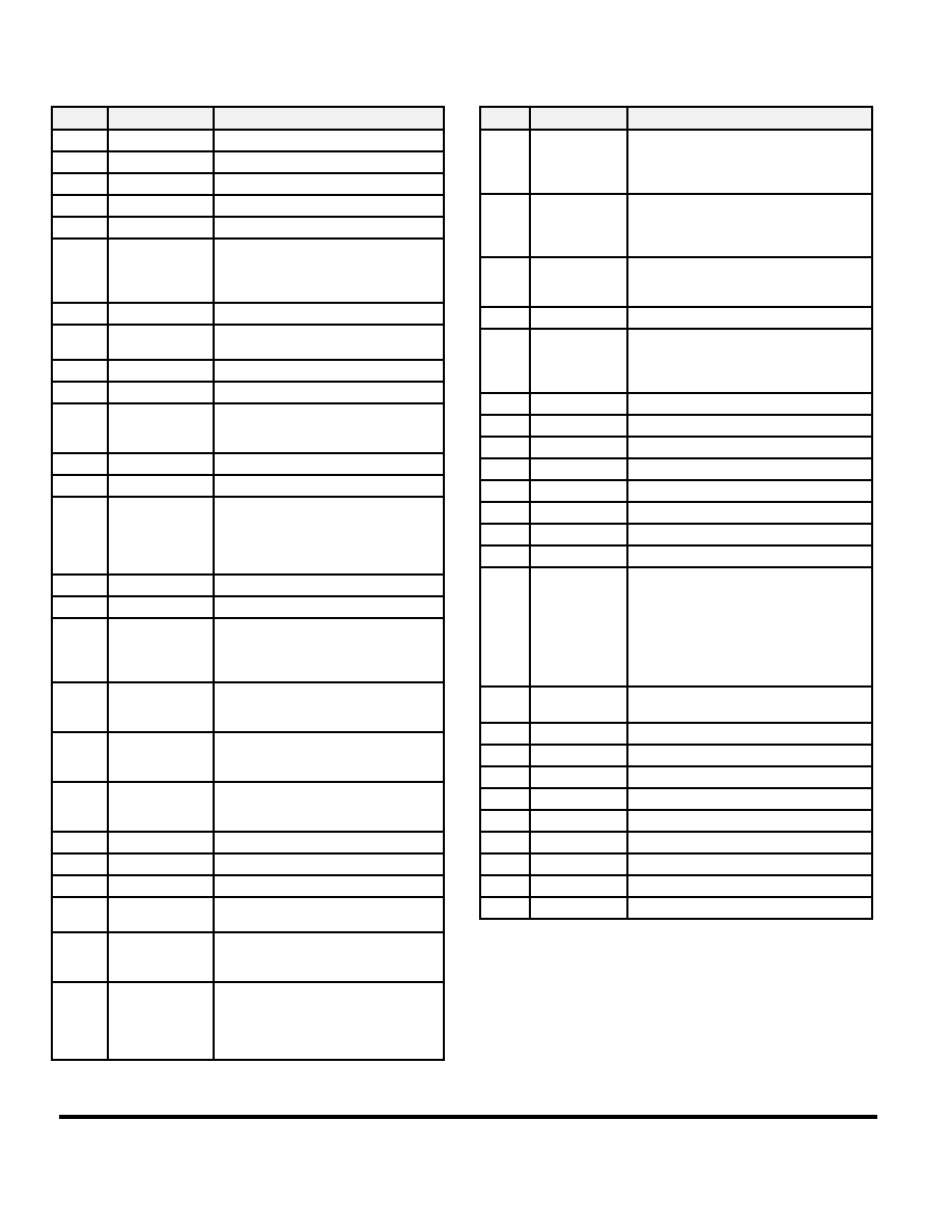
ELECTRICAL AND MECHANICAL SPECIFICATIONS
Characteristic
Value
Input Characteristics
Frequency Range
5 to 65 MHz (in 100 Hz steps)[DP1]
Modulation
Types
Differentially Encoded QPSK
Input Signal
Level
Scales with bit rate, see Table 1.
Burst-to-Burst
Variation
Greater then ±6 dB from the
nominally commanded level
Programmable
Input Level
Control
30 dB (1 dB Steps)
Input Noise
Level Max
0 dBmV
Input Impedance
75 Ohms
Return Loss
> 15 dB
PLL Tuning Time
Approx. 30 ms
Input Carrier
Freq. Accuracy
Computed using the formula:
R
s
* 1% - F
max
* 25 PPM
where:
R
s
=
±
Symbol Rate
F
max
= maximum carrier freq (in
MHz)
(e.g., for 1.28 Msps and 65 MHz
carrier, the required accuracy is
±11.8 kHz)
Composite Input
Level Maximum
TBD
Undesired Input
Power
-54 dBm for 66 to 74 MHz
-15 dBm above 74 MHz
Performance
RSSI Accuracy
±
2 dB
BER
1 x 10
-6
max. for E
b
/N
o
=13 dB
1 x 10
-9
max. for E
b
/N
o
=15 dB
Excess
Bandwidth
0.25 - 0.30
Channel Spacing
(1+
) X symbol rate
Guard Time
between Bursts
4 symbols min (See Figure 1)
11 symbols for variable packet
length mode
Preamble
14 symbols = 28 bits or
(00 00 00 00 11 11 00 00 11 11 00 11 00 11)
16 symbols = 32 bits or
(00 00 00 00 11 11 11 00 11 11 11 00 11 11 00 11)
16 symbols DAVIC or
(11 00 11 00 11 00 11 00 11 00 11 00 00 00 11 01)
14 symbols STEL-9244
(11 11 11 00 00 11 00 00 00 00 00 00 00 00)
Characteristic
Value
Data Rate
Variable with 1 kbit per second
resolution (see Table 1 for
examples)
Burst Length
Programmable from 32 to 8192
symbols (see Table 2) or variable
length
Probability of
Missed
Acquisition
10
-6
, for E
b
/N
o
= 13 dB, (signal
removed)
Signal Level = nominal
Probability of
False Acquisition
10
-6
per packet period,
for E
b
/N
o
= 13 dB,
Input Level = nominal
Carrier Frequency
Estimator
Eb/No = 9 dB:
Maximum
Carrier Offset
5% R
s
(R
s
=symbol rate)
Accuracy (mean
or bias)
mean
10% of carrier frequency
offset
Repeatability
(standard
deviation)
8% of carrier frequency offset
Eb/No = 13 dB:
Maximum
Carrier Offset
5% R
s
(R
s
=symbol rate)
Accuracy (mean
or bias)
mean
7% of carrier frequency
offset
Repeatability
(standard
deviation)
6% of carrier frequency offset
Master Clock Input
(Special Request
Option)
Frequency
25 MHz
Stability
±
25 ppm (min)
Duty Cycle
45/55
Supply Voltages
Digital (Typical)
+5 V
±
5 % @ 0.82 A
Analog (Typical)
+12 V
±
5 % @ 0.4 A
Environmental
Operating
Temperature
Range
0 to 70∞ C
Storage
Temperature
Range
-40 to +85∞ C
Mechanical
Dimensions
3.5" x 5.5" x 0.5"
Weight
< 1 pound
STEL-9257
6
Product Information
Table 1. Data Rates and Signal Levels
Burst
Allocated
Burst
Signal Level (dBmV)
Signal Level (dBmV)
Symbol
Rate
(Msps)
Bandwidth = Min
Carrier Spacing
(MHz)
Reference
Standard
QPSK Bit
Rate
(Mbps)
Min
Center
Max
Min
(including -6 dB
burst-to-burst)
Max
(including +6 dB
burst-to-burst)
0.128
0.166
DAVIC
0.256
-17
-2
13
-23
19
0.16
0.2
MCNS
0.32
-16
-1
14
-22
20
0.256
0.32
IEEE-802.14
0.512
-14
1
16
-20
22
0.32
0.4
MCNS
0.64
-13
2
17
-19
23
0.512
0.64
IEEE-802.14
1.024
-11
4
19
-17
25
0.64
0.8
MCNS
1.28
-10
5
20
-16
26
0.772
1.004
DAVIC
1.544
-9
6
21
-15
27
1.024
1.28
IEEE-802.14
2.048
-8
7
22
-14
28
1.28
1.6
MCNS
2.56
-7
8
23
-13
29
1.544
2.007
DAVIC
3.088
-6
9
24
-12
30
2.048
2.56
IEEE-802.14
4.096
-5
10
25
-11
31
2.56
3.2
MCNS
5.12
-4
11
26
-10
32
1
0.8
0.6
0.4
0.2
0
-0.2
-0.4
-0.6
-0.8
-1
Minimum Interburst Gap of 4 Symbols
0
1
2
3
4
Time after last Symbol of previous Burst
(symbols)
Figure 1. Burst Guard Time
Table 2. Mode Control Selection
Mode Control Pins
Pin 19 Pin 20
Pin 18
Mode of Operation
0
0
0
Disable Acquisition
0
0
1
"A" packet length
*
0
1
0
"B" packet length**
0
1
1
"C" packet length
1
0
0
"D" packet length
1
0
1
"E" packet length
1
1
0
"F" packet length
1
1
1
Variable Packet Length
Packet length is programmable
* Collision Length (See text)
** Default
Product Information
7
STEL-9257
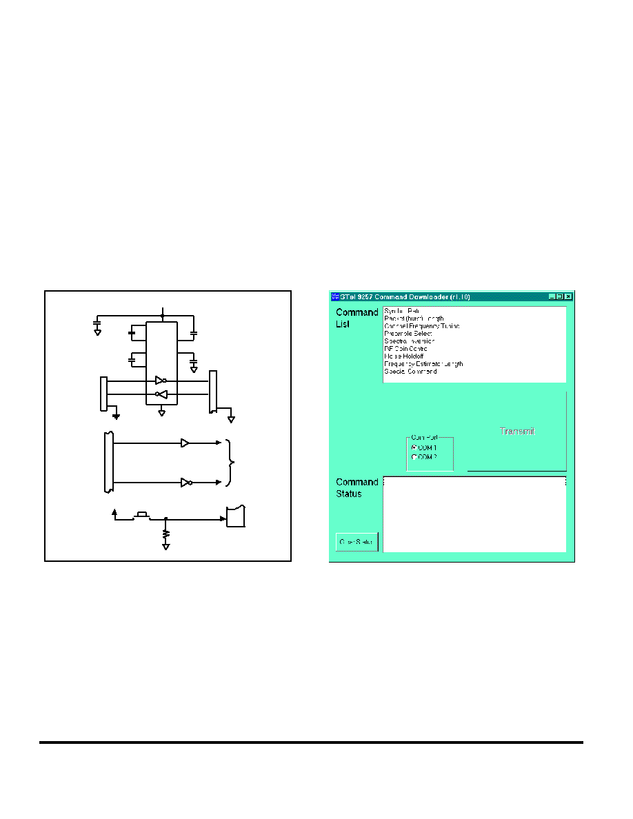
FUNCTIONAL DESCRIPTION
The STEL-9257 is a Burst QPSK Receiver designed for
fast acquisition of TDMA burst signals. Figure 2 shows
the three functional blocks of circuitry that comprise the
STEL-9257 ≠ Tuner, Digital Demod, and Microprocessor.
TUNER
The Tuner converts the RF input signal (5-65 MHz) into
an IF signal, which is then filtered by a Surface Acoustic
Wave (SAW) filter.
DIGITAL DEMOD
The Digital Demod is comprised of circuits that perform
four functions: Digital Preprocessing, Demodulation,
Synchronization and Estimation, and Timing and
Control.
The Digital Preprocessing circuitry samples the IF
signal, filters and decimates the samples, and then
outputs digital samples to the subsequent processing
blocks.
A FIR filter is used to filter the digital samples. The
STEL-9257 transmit spectrum is designed for
alpha = 0.25 - 0.30 (25% - 30% excess bandwidth)
square root raised cosine. The transmit FIR filter
coefficients shown in Figure 3 form a shaped/matched
filter for use with the STEL-1108 and STEL-1109 digital
QPSK Modulator chip.
5 - 65 MHz
Serial Control and Status
RESET
+5 VDC
Tuner
IF Signal
MODE0
DATAVAL
DATA
CLK
RSSI Bus
RSSIVAL
RSSI TYPE
RSSIEN
WCP 52710.c - 1/21/97
RSSINHOFF
GATED CLK
MODE1
+12 VDC
GND
MODE2
Digital
Demod
Board Enable
Microprocessor
FREQ EST. BUS
FREQVAL
Figure 2. Receiver Block Diagram
STEL-9257
8
Product Information
WCP 53701.c-10/29/97
0, 31
1, 30
2, 29
3, 28
4, 27
5, 26
6, 25
7, 24
8, 23
9, 22
10, 21
11, 20
12, 19
13, 18
14, 17
15, 16
9
-1
-16
-22
-10
18
43
41
2
-58
-99
-76
34
211
394
511
Figure 3. FIR Filter Coefficients (
= 0.25)
MICROPROCESSOR
Upon external reset, the Microprocessor configures the
Tuner and Digital Demod circuitry for operation. The
Microprocessor then waits for external serial port
commands. Each STEL-9257 is selected and enabled by
asserting the Board Enable control signal (BEN) low.
INPUT LEVEL DYNAMIC RANGE
The input level dynamic range of the receiver is a
function of E
b
/N
o
. In a typical data-over-CATV system,
the E
b
/N
o
ratio will increase as the transmit level is
increased. The STEL-9257 contains a programmable
gain amp to permit nominal input signal level
adjustment. The function can be controlled over a
30 dB range in 1 dB steps. Table 3 shows the values to
be downloaded to the 9257 using the RF Gain Control
command.
The STEL-9257 can maintain proper reception over an
approximate
±
6 dB range from nominal. Figure 4
shows the typical operational area. The S/N ratio can
be derived from the chart by subtracting the noise level
from the signal level. For QPSK modulation the E
b
/N
o
ratio can be calculated by subtracting 3 dB from the
S/N ratio.
ADAPTIVE THRESHOLD FUNCTION
(Patent Pending)
In order for the adaptive threshold function to operate
correctly, an occasional measurement of the
background channel noise must be made by the
STEL-9257. The measurement need only be performed
frequently enough (on the order of minutes) to allow
the STEL-9257 to track the average background channel
noise level. The measurement period is a function of
the RSSI integration length, which is a fixed at 191
symbols.
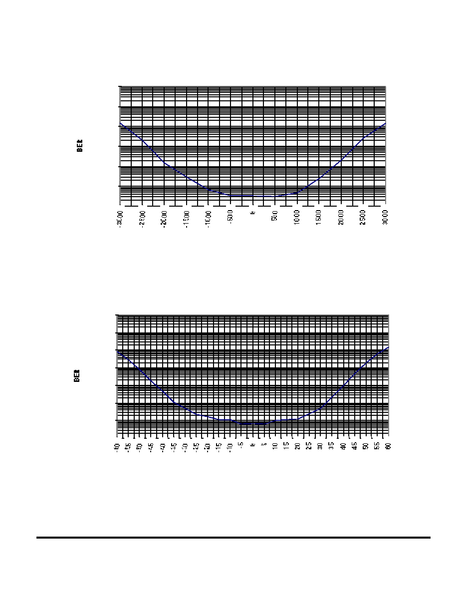
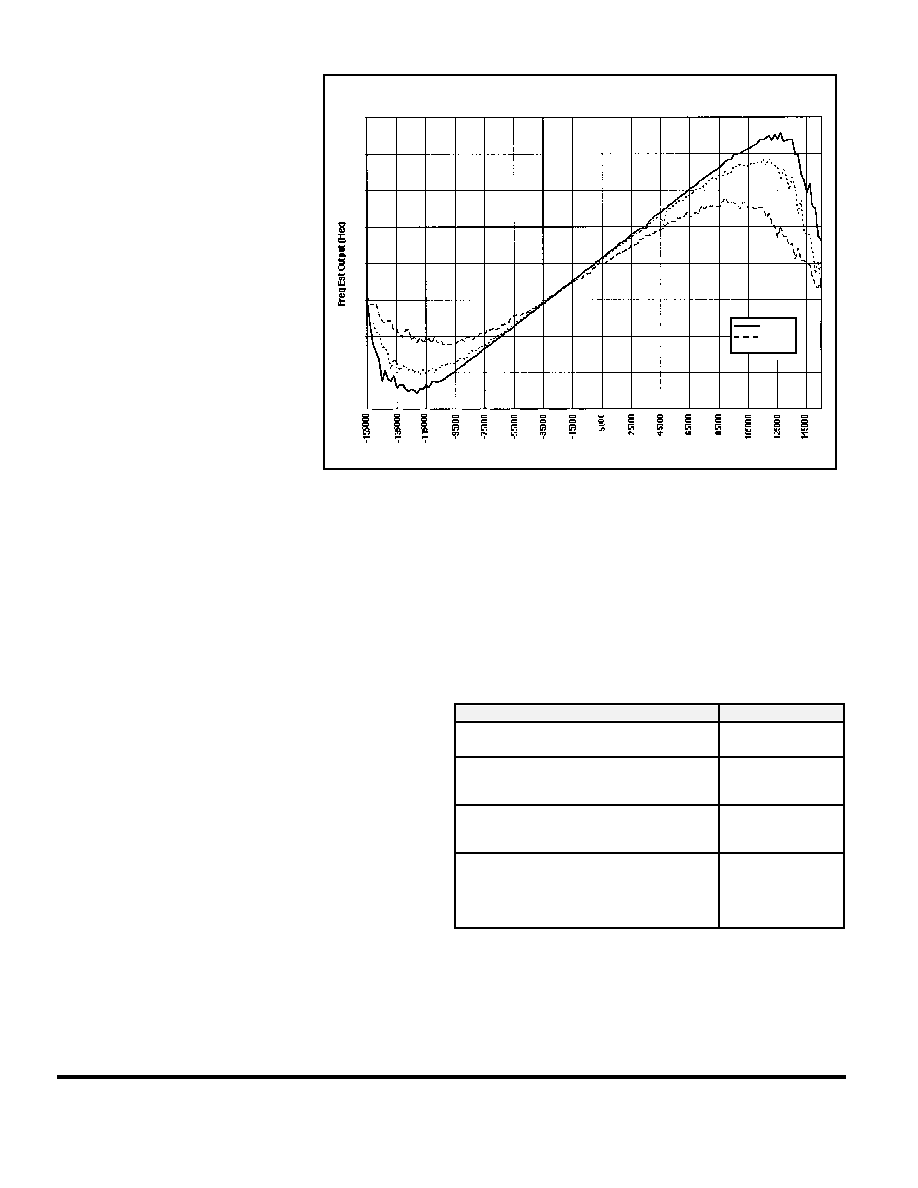
FREQUENCY ESTIMATOR
Since the bit error rate performance degrades as the
carrier frequency varies from ideal (See Figure 5 and
Figure 6), the 9257 incorporates a frequency estimator
function. The Frequency Estimator function provides
the user with an estimate of the received signal's
frequency error in the form 8 bit signed number. If the
received signal's frequency error is less than 5% of the
symbol rate, the Frequency Estimator bus will output a
frequency correction estimate that is accurate to within
7% of ideal. This function can be used to servo the
transmitter to the correct transmission frequency. See
the specification table for performance details. For a
performance example see Figure 7.
For net-entry, a registration burst consisting of BPSK-
like data, i.e. double each bit, can be used to improve
the performance of the Frequency Estimator. Note:
Frequency Estimator Output codes 127, 128, & 129
should be discarded and not used.
30
Signal
Level
20
10
0
-4
-50
-40
-30
-20
-10
0
Noise Level
(dBmV in Symbol Rate BW)
(dBmV)
Too Little Signal
Operational Area
Excessive
Noise
Signal Compression
WCP 52741.c-2/21/97
6
e-3
e-4
e-5
e-6
e-7
Figure 4. Burst Demod Dynamic Range (0.5 Msps case) (Preliminary)
Product Information
9
STEL-9257
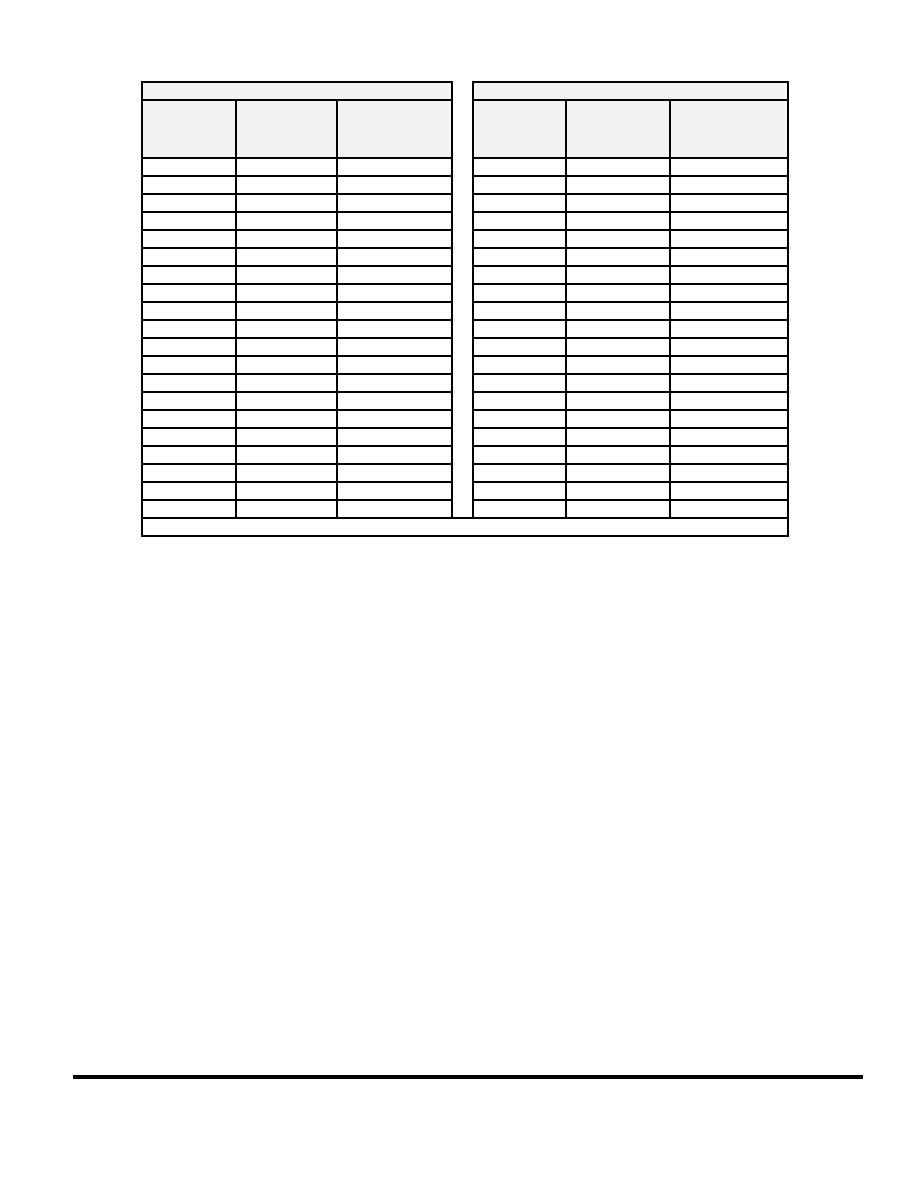
Table 3. Gain Setting Table
Nominal
RF Gain Setting For Symbol Rate =
Signal
Level
(dBmV)
.128
Msps
.160
Msps
.256
Msps
.320
Msps
.512
Msps
.640
Msps
.772
Msps
1.024
Msps
1.280
Msps
1544
Msps
2.048
Msps
2.560
Msps
26
54
25
57
59
24
60
62
64
23
62
65
67
69
22
64
67
70
72
74
21
67
69
72
75
77
79
20
68
72
74
77
80
82
84
19
69
73
77
79
82
85
87
89
18
74
78
82
84
87
90
92
94
17
72
79
83
87
89
92
95
97
99
16
73
77
84
88
92
94
97
100
102
104
15
78
82
89
93
97
99
102
105
107
109
14
74
83
87
94
98
102
104
107
110
112
114
13
75
79
88
92
99
103
107
109
112
115
117
119
12
80
84
93
97
104
108
112
114
117
120
122
124
11
85
89
98
102
109
113
117
119
122
125
127
129
10
90
94
103
107
114
118
122
124
127
130
132
134
9
95
99
108
112
119
123
127
129
132
135
137
139
8
100
104
113
117
124
128
132
134
137
140
142
144
7
105
109
118
122
129
133
137
139
142
145
147
149
6
110
114
123
127
134
138
142
144
147
150
152
154
5
115
119
128
132
139
143
147
149
152
155
157
159
4
120
124
133
137
144
148
152
154
157
160
162
164
3
125
129
138
142
149
153
157
159
162
165
167
169
2
130
134
143
147
154
158
162
164
167
170
172
174
1
135
139
148
152
159
163
167
169
172
175
177
179
0
140
144
153
157
164
168
172
174
177
180
182
184
-1
145
149
158
162
169
173
177
179
182
185
187
189
-2
150
154
163
167
174
178
182
184
187
190
192
194
-3
155
159
168
_172
179
183
187
189
192
195
197
199
-4
160
164
173
177
184
188
192
194
197
200
202
204
-5
165
169
178
182
189
193
197
199
202
205
207
-6
170
174
183
187
194
198
202
204
207
210
-7
175
179
188
192
199
203
207
209
212
-8
180
184
193
197
204
208
212
214
-9
185
189
198
202
209
213
217
-10
190
194
203
207
214
218
-11
195
199
208
212
219
-12
200
204
213
217
-13
205
209
218
222
-14
210
214
223
-15
215
219
-16
220
224
-17
225
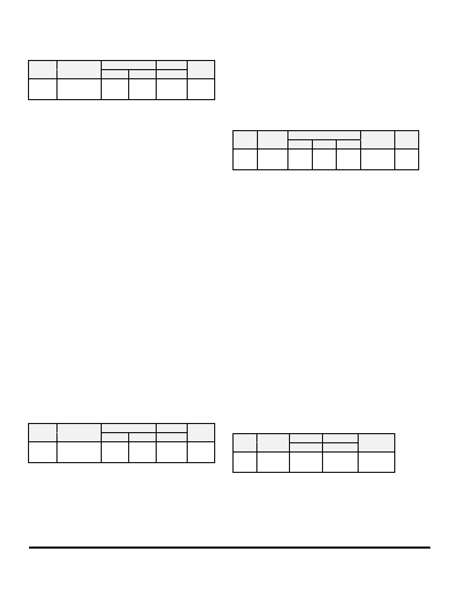
MODE CONTROL
The STEL-9257 can be disabled, operated in the fixed
packet length mode, or operated in the variable
packet length mode. The mode control signals (Mode
0, Mode 1, and Mode 2) must be set as for the desired
mode of operation.
In the fixed packet length mode, the user may select
six different packet lengths for the expected input
signal packet length.
In the variable packet length mode, the STEL-9257
automatically detects the end of the data transmission
burst (EOB). The EOB detection process prevents the
DataValid signal from precisely framing the end of
the packet, and also requires the guard time between
data packets be set to a minimum of 11 symbols. See
Table 2 for more details.
Note that, per the MCNS spec, the headend MAC
always knows the length of each upstream packet
and should give this information to the headend
receiver.
STEL-9257
10
Product Information
Example of Frequency Offset Performance,
Signal Level = Nominal - 6 dB, Eb/No = 12.5 dB, 0.128 Msps
1.00E-06
1.00E-05
1.00E-04
1.00E-03
1.00E-02
1.00E-01
1.00E+00
Offset(Hz)
Figure 5. Example of BER vs Frequency Offset for .128 Msps
Example of Frequency Offset Performance, 2.56 Msps,
Signal Level = Nominal, Eb/No = 12.5 dB
1.00E-07
1.00E-06
1.00E-05
1.00E-04
1.00E-03
1.00E-02
1.00E-01
1.00E+00
Offset(kHz)
Figure 6. Example of BER vs Frequency Offset for 2.56 Msps
Product Information
11
STEL-9257
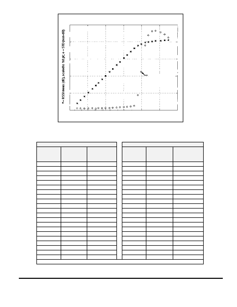
RSSI
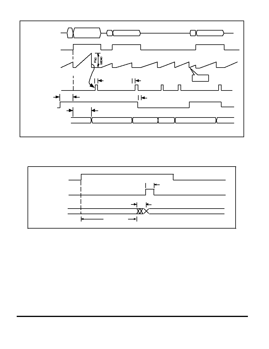
Figure 13 shows the timing
relationship between the RF input
signal into the STEL-9257 and the
received signal strength indicator
(RSSI) signals output from the
STEL-9257.
An RSSI Signal/Noise Accumulator
measures the RF input signal
power during a burst and the noise
power between bursts. The
accumulator integrates a sample of
the RF input signal for a period of
M1 symbols and the noise for a
period of M2 symbols (M1 and M2
default values are both fixed at 191
symbols). The RF input signal path
is temperature compensated, and
the analog supply has local
regulation, in order to provide an
RSSI measurement accuracy of ± 2
dB over a temperature range of 0 to
70∞C. The RSSI DATA bus outputs
the RSSI measurement as a parallel,
8-bit value (RSSI0-RSSI7). Use the
RSSI signal and noise strength look-up tables (Table 4
through Table 15) to convert the resulting hexadecimal
(8 bit) RSSI value to an absolute power reading. (Note:
The Standard Deviation is the expected variation in the
RSSI measurement in units of LSB's. The absolute
power values are based on a 75-ohm system.)Driving
the RSSI Enable (RSSIEN) signal low enables the RSSI
outputs. The RSSIVAL pulse latches in the RSSI DATA.
Read the RSSI TYPE to determine if the value is a signal
or noise measurement.
The absolute power measured is determined relative to
the amount of gain that the 9257's variable gain amp. is
programmed for. For example: for 0.128 Msps and a
programmed nominal input level of + 10 dBmV (gain
setting = 90), G = 13 - 10 = 3. If the RSSI Value = 72 hex,
then the absolute power is 17- G = 17-3 = 14 dBmV.
For an example of the RSSI measurement behavior see
Figure 8.
Noise measurements can be turned off by asserting
noisehold (pin 17). They also may be delayed for the
purpose of synchronization to time-slot boundries by
asserting RSSINHOFF (Pin 23), or by programming the
Noise Holdoff register to a non-zero value.
COLLISION
The collision output signal, Pin 40, is asserted when RF
input energy is detected, but a valid signal is either not
present, or is somehow corrupted. The following
scenarios may cause collision to be asserted.
Condition
Action
1) A strong noise burst occurs when no
CM is transmitting
Ignore collision
2) A noise burst occurs during the
preamble of a CM transmission. No
Data Valid is asserted.
Retransmit
Packet
3) A CM transmits during the preamble
of another CM packet. No Data Valid
is asserted.
Resync CM and
request
retransmission
4) A CM transmits during the data
portion of another CM packet, thus
corrupting the desired data and
continuing transmission after the first
packet ends. Data Valid is asserted
Resync CM and
request
retransmission
The collision signal stays high for the length of time
programmed into the collision register (command
ID = 0Bh).
TPG 53234.c-7/11/97
Example of Frequency Estimator Performance
For 1.28 Msps (100 Point Average)
Freq Offset (Hz)
80
60
40
20
0
-20
-40
-60
-80
No Noise
9 Eb/No
13 Eb/No
∑ ∑ ∑ ∑ ∑ ∑
Figure 4A
Figure 7. Example for 1.28 Msps (100 point averages)
STEL-9257
12
Product Information
TPG 53235.c-7/11/97
0
5
10
15
20
25
30
Input level (dBmV), 128 ksps
0
5
10
15
20
25
Standard Deviation
of Measurement
Increases When
Internal Bus Limits.
Example of 9257 Signal RSSI Measurement Behavior
Figure 8. Example of STEL-9257 Signal RSSI Measurement Behavior
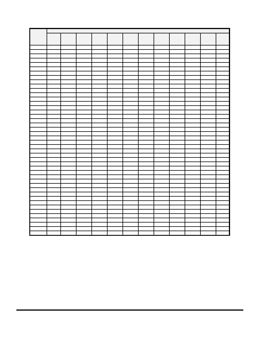
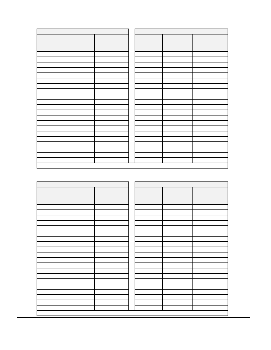
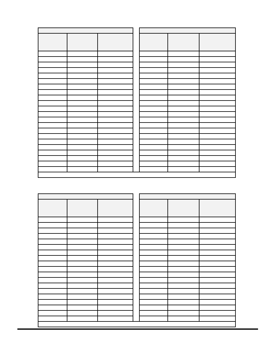
Table 4. 0.128 Msps, RSSI Signal Conversion Table
Signal
Noise
RSSI Value
(Hex)
Typical
Standard
Deviation
(LSB)
Absolute Power
(dBmV)
RSSI Value
(Hex)
Typical
Standard
Deviation
(LSB)
Absolute Power
(dBmV)
15
0.5
3-G
15
1.0
-9-G
18
0.5
4-G
17
1.0
-8-G
1B
0.5
5-G
1A
1.0
-7-G
1E
0.5
6-G
1D
1.0
-6-G
22
0.5
7-G
21
1.5
-5-G
27
0.5
8-G
24
1.5
-4-G
2C
0.5
9-G
29
2.0
-3-G
31
0.5
10-G
2E
2.0
-2-G
39
0.5
11-G
34
2.0
-1-G
41
0.5
12-G
3A
2.0
0-G
47
0.5
13-G
42
2.5
1-G
51
0.5
14-G
49
3.0
2-G
5B
0.5
15-G
52
3.0
3-G
66
0.5
16-G
5B
3.0
4-G
72
0.5
17-G
68
4.0
5-G
83
0.5
18-G
74
5.0
6-G
8C
0.5
19-G
9D
0.5
20-G
B1
0.5
21-G
C2
1.0
22-G
CD
1.5
23-G
G = 13 - Nominal Input Signal Level Corresponding to RF Gain Setting (dBmV)
Product Information
13
STEL-9257
Table 5. 0.160 Msps, RSSI Signal Conversion Table
Signal
Noise
RSSI Value
(Hex)
Typical
Standard
Deviation
(LSB)
Absolute Power
(dBmV)
RSSI Value
(Hex)
Typical
Standard
Deviation
(LSB)
Absolute Power
(dBmV)
13
0.5
2-G
C
0.5
-15-G
15
0.5
3-G
C
0.5
-14-G
17
0.0
4-G
D
0.5
-13-G
1B
0.5
5-G
F
0.5
-12-G
1E
0.5
6-G
10
1.0
-11-G
22
0.5
7-G
12
1.0
-10-G
27
0.5
8-G
14
0.5
-9-G
2B
0.5
9-G
17
1.0
-8-G
31
0.5
10-G
19
1.0
-7-G
37
0.5
11-G
1C
1.0
-6-G
3E
0.5
12-G
20
1.5
-5-G
45
0.5
13-G
23
1.0
-4-G
4F
0.5
14-G
28
1.5
-3-G
58
0.5
15-G
2F
2.0
-2-G
63
0.5
16-G
34
2.5
-1-G
6F
0.5
17-G
3B
2.0
0-G
81
1.0
18-G
42
2.5
1-G
92
1.0
19-G
48
2.5
2-G
A3
1.0
20-G
50
3.0
3-G
B5
1.0
21-G
5A
3.5
4-G
C5
4.5
22-G
65
3.5
5-G
G = 14 - Nominal Input Signal Level Corresponding to RF Gain Setting (dBmV)
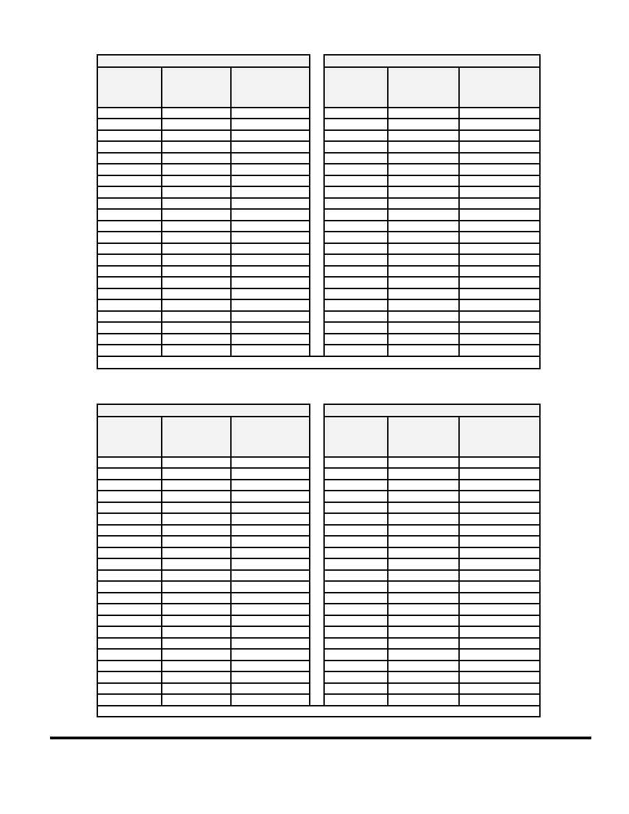
Table 6. 0.256 Msps, RSSI Signal Conversion Table
Signal
Noise
RSSI Value
(Hex)
Typical
Standard
Deviation
(LSB)
Absolute Power
(dBmV)
RSSI Value
(Hex)
Typical
Standard
Deviation
(LSB)
Absolute Power
(dBmV)
18
0.5
4-G
F
1.0
-13-G
1A
0.0
5-G
F
0.5
-12-G
1D
0.5
6-G
10
0.5
-11-G
21
0.5
7-G
12
1.0
-10-G
26
0.5
8-G
14
1.0
-9-G
2A
0.5
9-G
16
1.0
-8-G
2F
0.5
10-G
19
1.0
-7-G
36
0.5
11-G
1C
1.0
-6-G
3C
0.5
12-G
1F
1.0
-5-G
44
0.5
13-G
23
1.5
-4-G
4C
0.5
14-G
27
1.5
-3-G
56
0.5
15-G
2C
2.0
-2-G
61
0.5
16-G
34
2.0
-1-G
6C
0.5
17-G
3A
2.5
0-G
7A
1.0
18-G
41
2.5
1-G
87
1.0
19-G
49
3.0
2-G
97
1.0
20-G
4E
2.5
3-G
A9
1.0
21-G
58
3.5
4-G
BB
1.0
22-G
63
4.0
5-G
6F
3.5
6-G
G = 16 - Nominal Input Signal Level Corresponding to RF Gain Setting (dBmV)
STEL-9257
14
Product Information
Table 7. 0.320 Msps, RSSI Signal Conversion Table
Signal
Noise
RSSI Value
(Hex)
Typical
Standard
Deviation
(LSB)
Absolute Power
(dBmV)
RSSI Value
(Hex)
Typical
Standard
Deviation
(LSB)
Absolute Power
(dBmV)
12
0.5
2-G
E
1.0
-15-G
14
0.0
3-G
C
0.5
-14-G
17
0.5
4-G
E
1.0
-13-G
19
0.5
5-G
E
0.5
-12-G
1D
0.5
6-G
10
0.5
-11-G
21
0.5
7-G
11
1.0
-10-G
24
0.5
8-G
14
1.0
-9-G
29
0.5
9-G
15
1.0
-8-G
2E
0.5
10-G
18
1.0
-7-G
34
0.5
11-G
1B
1.0
-6-G
3A
0.5
12-G
1E
1.0
-5-G
42
0.5
13-G
22
1.5
-4-G
4B
0.5
14-G
26
1.5
-3-G
53
0.5
15-G
2A
2.0
-2-G
5E
3.0
16-G
32
2.0
-1-G
69
0.5
17-G
39
2.5
0-G
75
1.0
18-G
3F
2.5
1-G
82
0.5
19-G
43
2.5
2-G
93
1.0
20-G
4C
3.0
3-G
A4
1.0
21-G
56
3.0
4-G
B6
1.5
22-G
60
3.5
5-G
C7
6.5
23-G
G = 17 - Nominal Input Signal Level Corresponding to RF Gain Setting (dBmV)
Table 8. 0.512 Msps, RSSI Signal Conversion Table
Signal
Noise
RSSI Value
(Hex)
Typical
Standard
Deviation
(LSB)
Absolute Power
(dBmV)
RSSI Value
(Hex)
Typical
Standard
Deviation
(LSB)
Absolute Power
(dBmV)
15
0.5
4-G
D
0.5
-13-G
17
0.5
5-G
D
0.5
-12-G
1A
0.5
6-G
10
0.5
-11-G
1E
0.5
7-G
11
1.0
-10-G
21
0.5
8-G
12
1.0
-9-G
26
0.5
9-G
14
1.0
-8-G
2B
0.5
10-G
16
1.0
-7-G
30
0.5
11-G
19
1.0
-6-G
36
0.5
12-G
1C
1.0
-5-G
3D
0.5
13-G
1F
1.5
-4-G
44
0.5
14-G
23
1.5
-3-G
4D
0.5
15-G
27
1.5
-2-G
56
0.5
16-G
2C
2.0
-1-G
61
0.5
17-G
31
2.0
0-G
6D
1.0
18-G
3B
2.5
1-G
79
0.5
19-G
3E
2.5
2-G
87
1.0
20-G
46
2.5
3-G
98
1.0
21-G
4F
2.5
4-G
A9
1.0
22-G
59
3.0
5-G
C1
4.0
23-G
64
4.0
6-G
C9
7.0
24-G
70
4.0
7-G
D4
14.5
25-G
G = 19 - Nominal Input Signal Level Corresponding to RF Gain Setting (dBmV)
Product Information
15
STEL-9257
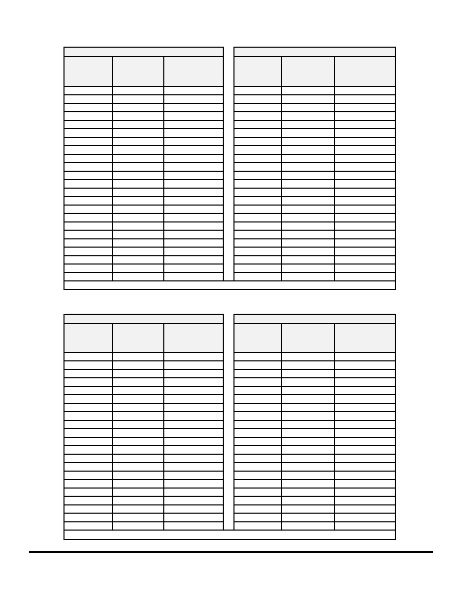
Table 9. 0.640 Msps, RSSI Signal Conversion Table
Signal
Noise
RSSI Value
(Hex)
Typical
Standard
Deviation
(LSB)
Absolute Power
(dBmV)
RSSI Value
(Hex)
Typical
Standard
Deviation
(LSB)
Absolute Power
(dBmV)
12
0.0
9-G
9
0.5
-8-G
14
0.5
10-G
A
0.5
-7-G
17
0.0
11-G
C
0.5
-6-G
1A
0.5
12-G
E
0.5
-5-G
1D
0.0
13-G
F
0.5
-4-G
21
0.5
14-G
11
0.5
-3-G
25
0.5
15-G
13
1.0
-2-G
29
0.5
16-G
15
1.0
-1-G
2F
0.5
17-G
18
1.0
0-G
35
0.5
18-G
1B
1.0
1-G
3A
0.5
19-G
1E
1.0
2-G
41
0.5
20-G
23
1.5
3-G
49
0.5
21-G
26
1.5
4-G
52
0.5
22-G
2A
2.0
5-G
5D
1.0
23-G
30
2.0
6-G
67
0.5
24-G
39
2.0
7-G
73
0.5
25-G
40
2.5
8-G
82
1.0
26-G
44
2.5
9-G
8C
1.5
27-G
4C
3.5
10-G
99
3.0
28-G
56
3.0
11-G
AB
2.5
29-G
60
3.5
12-G
D4
14.5
25-G
6B
4.0
13-G
7E
6.5
14-G
G = 20 - Nominal Input Signal Level Corresponding to RF Gain Setting (dBmV)
Table 10. 0.772 Msps, RSSI Signal Conversion Table
Signal
Noise
RSSI Value
(Hex)
Typical
Standard
Deviation
(LSB)
Absolute Power
(dBmV)
RSSI Value
(Hex)
Typical
Standard
Deviation
(LSB)
Absolute Power
(dBmV)
1C
0.0
13-G
F
0.5
-4-G
20
0.0
14-G
10
0.5
-3-G
24
0.5
15-G
12
1.0
-2-G
29
0.5
16-G
15
1.0
-1-G
2E
0.5
17-G
17
1.0
0-G
33
0.5
18-G
1A
1.0
1-G
39
0.5
19-G
1D
1.0
2-G
42
0.5
20-G
21
1.0
3-G
47
0.5
21-G
25
1.5
4-G
4F
0.5
22-G
2A
1.5
5-G
5A
0.5
23-G
2F
1.5
6-G
65
0.5
24-G
35
2.0
7-G
70
0.5
25-G
3B
2.5
8-G
74
1.0
26-G
42
2.5
9-G
81
1.0
27-G
4B
3.0
10-G
96
2.5
28-G
54
3.5
11-G
A1
4.5
29-G
5D
3.5
12-G
AB
6.5
30-G
6A
4.5
13-G
76
5.0
14-G
84
5.0
15-G
8E
6.5
16-G
G = 21 - Nominal Input Signal Level Corresponding to RF Gain Setting (dBmV)
STEL-9257
16
Product Information
Table 11. 1.024 Msps, RSSI Signal Conversion Table
Signal
Noise
RSSI Value
(Hex)
Typical
Standard
Deviation
(LSB)
Absolute Power
(dBmV)
RSSI Value
(Hex)
Typical
Standard
Deviation
(LSB)
Absolute Power
(dBmV)
17
0.5
12-G
C
0.5
-5-G
1A
0.5
13-G
E
0.5
-4-G
1E
0.5
14-G
F
1.0
-3-G
22
0.5
15-G
11
1.0
-2-G
26
0.5
16-G
13
1.0
-1-G
2A
0.5
17-G
15
1.0
0-G
30
0.5
18-G
19
1.0
1-G
34
0.5
19-G
1B
1.0
2-G
3B
0.5
20-G
1F
1.0
3-G
43
0.5
21-G
22
1.5
4-G
4A
0.5
22-G
27
2.0
5-G
54
0.5
23-G
2C
1.5
6-G
61
0.5
24-G
31
2.0
7-G
68
1.0
25-G
39
2.0
8-G
75
1.0
26-G
41
2.5
9-G
82
1.0
27-G
46
3.0
10-G
8F
1.5
28-G
4E
3.0
11-G
9A
3.5
29-G
59
3.5
12-G
63
4.0
13-G
6F
4.0
14-G
G = 22 - Nominal Input Signal Level Corresponding to RF Gain Setting (dBmV)
Table 12. 1.280 Msps, RSSI Signal Conversion Table
Signal
Noise
RSSI Value
(Hex)
Typical
Standard
Deviation
(LSB)
Absolute Power
(dBmV)
RSSI Value
(Hex)
Typical
Standard
Deviation
(LSB)
Absolute Power
(dBmV)
16
0.5
12-G
C
0.5
-5-G
19
0.5
13-G
D
0.5
-4-G
1C
0.5
14-G
E
0.5
-3-G
20
0.5
15-G
10
0.5
-2-G
24
0.5
16-G
12
1.0
-1-G
29
0.5
17-G
14
1.0
0-G
2D
0.5
18-G
17
1.0
1-G
32
0.5
19-G
1A
1.0
2-G
38
0.5
20-G
1D
1.0
3-G
41
0.5
21-G
21
1.5
4-G
47
0.5
22-G
25
1.5
5-G
50
0.5
23-G
29
1.5
6-G
59
1.0
24-G
31
2.0
7-G
64
1.0
25-G
37
2.0
8-G
70
1.0
26-G
3B
2.0
9-G
7F
1.0
27-G
42
2.5
10-G
89
1.0
28-G
4A
2.5
11-G
95
2.5
29-G
53
3.0
12-G
A2
5.0
30-G
5E
3.5
13-G
68
4.0
14-G
G = 23 - Nominal Input Signal Level Corresponding to RF Gain Setting (dBmV)
Product Information
17
STEL-9257
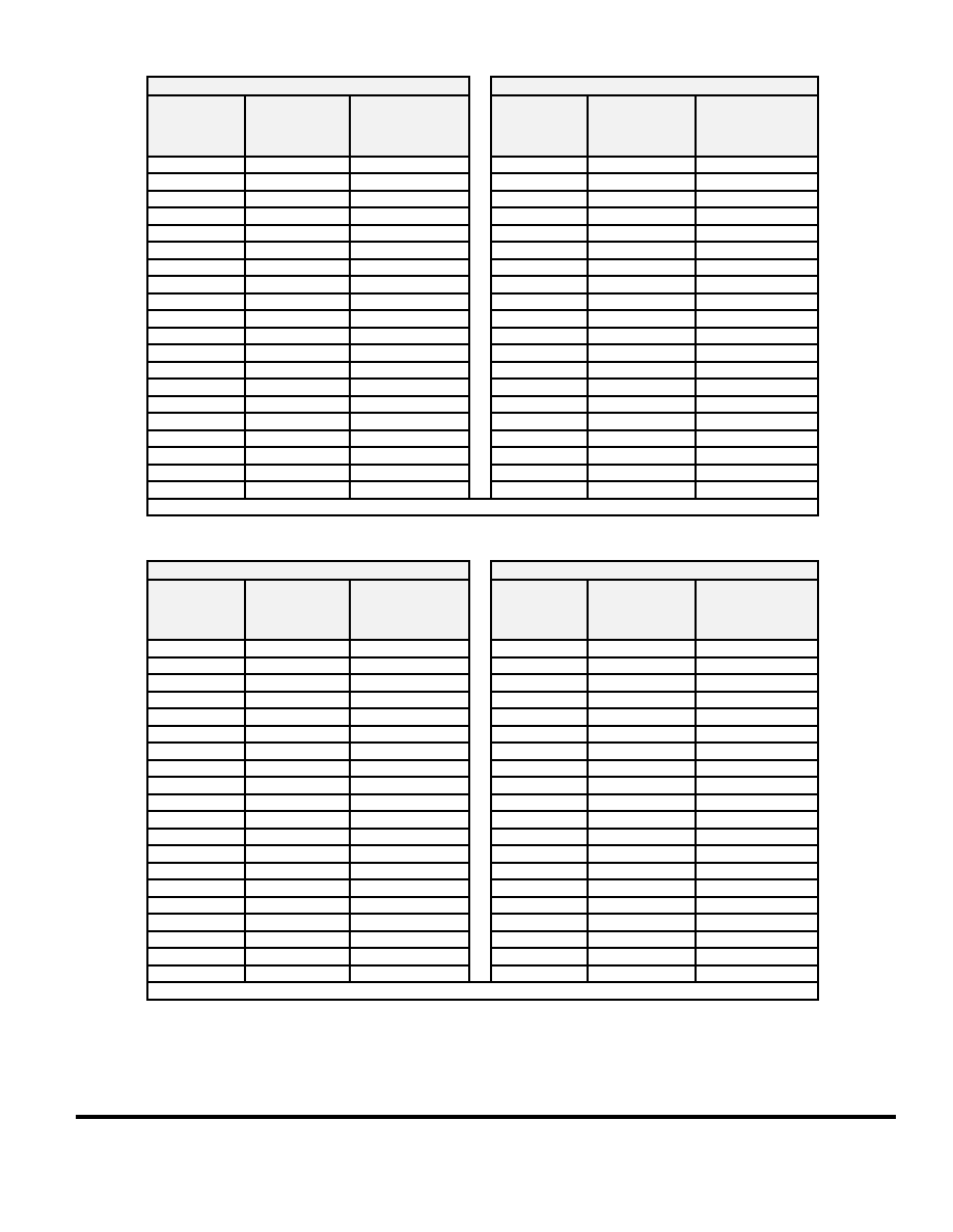
Table 13. 1.544 Msps, RSSI Signal Conversion Table
Signal
Noise
RSSI Value
(Hex)
Typical
Standard
Deviation
(LSB)
Absolute Power
(dBmV)
RSSI Value
(Hex)
Typical
Standard
Deviation
(LSB)
Absolute Power
(dBmV)
18
0.5
12-G
B
0.5
-6-G
1B
0.5
13-G
D
0.5
-5-G
1F
0.5
14-G
E
0.5
-4-G
22
0.5
15-G
10
0.5
-3-G
26
0.5
16-G
12
1.0
-2-G
2C
0.5
17-G
14
1.0
-1-G
31
0.5
18-G
16
1.0
0-G
36
0.5
19-G
19
1.0
1-G
3D
0.5
20-G
1C
1.0
2-G
44
0.5
21-G
1F
1.5
3-G
4C
0.5
22-G
24
1.5
4-G
57
0.5
23-G
28
1.5
5-G
62
1.0
24-G
2C
1.5
6-G
6C
1.0
25-G
32
2.0
7-G
78
1.0
26-G
39
2.5
8-G
84
1.0
27-G
3F
2.0
9-G
93
1.0
28-G
47
3.0
10-G
A4
1.5
29-G
50
3.5
11-G
BC
1.0
30-G
5A
3.5
12-G
C9
6.5
31-G
65
4.0
13-G
71
4.0
14-G
84
5.5
15-G
G = 24 - Nominal Input Signal Level Corresponding to RF Gain Setting (dBmV)
Table 14. 2.048 Msps, RSSI Signal Conversion Table
Signal
Noise
RSSI Value
(Hex)
Typical
Standard
Deviation
(LSB)
Absolute Power
(dBmV)
RSSI Value
(Hex)
Typical
Standard
Deviation
(LSB)
Absolute Power
(dBmV)
1C
0.5
14-G
F
0.5
-3-G
20
0.5
15-G
11
1.0
-2-G
24
0.5
16-G
12
1.0
-1-G
28
0.5
17-G
15
1.0
0-G
2D
0.5
18-G
18
1.0
1-G
32
0.5
19-G
19
1.0
2-G
38
0.5
20-G
1E
1.0
3-G
4
0.5
21-G
21
1.5
4-G
46
0.5
22-G
25
1.5
5-G
4F
0.5
23-G
29
2.0
6-G
58
0.5
24-G
2F
2.0
7-G
62
1.0
25-G
34
2.0
8-G
72
1.0
26-G
3D
2.5
9-G
7B
1.0
27-G
42
2.5
10-G
89
1.0
28-G
49
2.5
11-G
99
1.0
29-G
52
3.0
12-G
A9
1.5
30-G
5D
4.0
13-G
B8
4.5
31-G
69
4.0
14-G
76
4.5
15-G
G = 25 - Nominal Input Signal Level Corresponding to RF Gain Setting (dBmV)
STEL-9257
18
Product Information
Table 15. 2.560 Msps, RSSI Signal Conversion Table
Signal
Noise
RSSI Value
(Hex)
Typical
Standard
Deviation
(LSB)
Absolute Power
(dBmV)
RSSI Value
(Hex)
Typical
Standard
Deviation
(LSB)
Absolute Power
(dBmV)
17
0.5
13-G
D
0.5
-4-G
1A
0.5
14-G
E
0.5
-3-G
1D
0.5
15-G
10
0.5
-2-G
21
0.5
16-G
11
1.0
-1-G
25
0.5
17-G
14
1.0
0-G
29
0.5
18-G
14
1.0
1-G
2E
0.5
19-G
18
1.0
2-G
33
0.5
20-G
1A
1.0
3-G
3A
0.5
21-G
1D
1.0
4-G
41
0.5
22-G
22
1.0
5-G
48
0.5
23-G
25
1.5
6-G
52
1.0
24-G
2B
1.5
7-G
5C
1.0
25-G
30
2.0
8-G
66
1.0
26-G
36
2.0
9-G
72
1.0
27-G
40
2.5
10-G
84
1.0
28-G
43
3.0
11-G
8E
1.0
29-G
4C
3.0
12-G
9C
4.0
30-G
56
3.0
13-G
B3
4.5
31-G
60
3.5
14-G
BA
5.0
32-G
6C
4.5
15-G
G = 26 - Nominal Input Signal Level Corresponding to RF Gain Setting (dBmV)
Product Information
19
STEL-9257
STEL-9257 BENCH TEST
Configure the STEL-9257 for bench tests by removing
it from the host system. Attach a test fixture to the
STEL-9257 (see the schematic diagram, Figure 9). The
test fixture interfaces the STEL-9257 to a Bit Error
Rate Tester and Computer. Additional test equipment
is also required for DC power and RF input signal
generation.
The computer may use a factory supplied Graphical
User Interface (GUI) (see Figure 10) to format and
send commands from an external PC to the STEL-
9257 and to display command status bytes.
∑
The user selects an available PC COM Port (COM
1 or COM 2). If all COM ports are busy, an error
message will display on the PC monitor.
∑
The Command List displays the list of available
commands. Mouse-clicking on one of the
commands allows the user to select from a list of
options or to input parameter values in an input
field.
∑
The parameter units are displayed to the left of
the input field.
∑
The Transmit button sends the input command
values.
∑
The Command Status window displays the status
bytes from the STEL-9257.
∑
The Clear Status button clears the Command
Status window.
WCP 52712.c-9/10/97
+
0.1 uf
0.1 uf
1
+
Max
232A
0.1 uf
4
5
+
16
0.1 uf
2
6
0.1 uf
+
+
8
7
9
10
J3
15
3
2
5
6
8
To STEL-9257
UART Serial
Data Input/Output
DATAOUT
J3
24
31
GATEDCLK
To Bit Error
Rate Tester
From STEL-9257
Data and Gated
Clock Outputs
9 Pin "D" Female
From Computer
RS-232 Port
(or other Control
Device)
RESET
+5V
J3-11
To STEL-9257
Reset Input
100
+5V
3
14
Board
Enable
Figure 9. STEL-9257 Simple Test Fixture
Figure 10. GUI
STEL-9257
20
Product Information
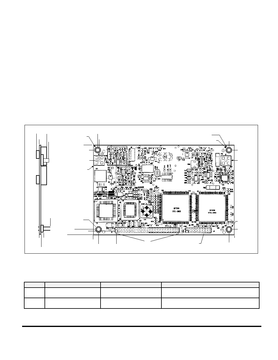
MECHANICAL CHARACTERISTICS
Figure 11 shows the layout dimensions of the
STEL-9257.
MOUNTING
The STEL-9257's overall dimensions of 3.5" x 5.5" x 0.5"
allow mounting as a daughter card. There are four
mounting holes, one at each corner of the circuit card.
A bottom clearance of 0.125 inches is required so
standoffs are required when mounting the STEL-9257
as a daughter board or in a chassis. Note the mounting
hardware dimensions (standoffs, washers, etc.) to
ensure that the adjacent traces, pads, and component
leads are not shorted out by exceeding the mounting
pads' diameters (0.25 in). In allocating mounting space,
the primary factors to consider are air flow for cooling
and clearance for the interconnecting cable connectors
and cable bend radii.
SHIELDING
RF shielding is provided for portions of the STEL-9257
circuitry, however if used in an EMI environment,
additional shielding may be required due to the low
signal sensitivity of the STEL-9257.
INTERFACE CONNECTORS
Table 15 lists the STEL-9257 interface connectors by
reference designator, and provides the part number
(P/N) and purpose of each connector. Pin-out data for
multi-contact connectors is provided by Table 16.
0.125
0
0
0.064
0.120
0.318
0.250
0.300
0
0.200
0.900
5.300
5.500
0.200
0.200
0.200
0.120 in. dia, 4 places
0.175
0.225
3.500
3.300
2.900
TPG 53452.c-9/8/97
Ground
Not Grounded
0.250 in. clearance
For test,
not loaded
Not Grounded
J1
J3
For test,
not loaded
0
0.200
Ground
0.125
Figure 11. Board Mechanical Layout
Table 15. I/O Connectors
Ref. Des.
P/N
Purpose/Signal Name
Remarks
J1
Applied Engineering,
2009-1511-000
SIGNAL IN (5-65 MHz Input)
SMB
J3
Digikey, S2211-25-ND
Digital I/O and Power
A single 50-pin connector, see Table 16 for pin
definitions.
Product Information
21
STEL-9257
Table 16. J3 Pin Definitions
Pin #
Signal Name
Description
1
+5V
Digital Power
2
+5V
Digital Power
3
+12V
Analog Power
4
GND
Ground
5
+12V
Analog Power
6
RXDATA
Input. Serial Data Input for
configuring the STEL-9257 (i.e.,
download commands). 10 K
pullup.
7
GND
Ground
8
TXDATA
Output. Serial status data from
STEL-9257.
9
+5V
Digital Power
10
GND
Ground
11
RESET
Input. Active high. Must be held
high for >100 us after STEL-9257
is powered up. 10 K pullup.
12
GND
Ground
13
+5V
Digital Power
14
BEN
Input. Board Enable, Active Low.
For each serial command byte
sent, BEN is polled. Command
bytes are ignored if BEN is high.
10 K pullup.
15
GND
Ground
16
GND
Ground
17
NOISEHOLD
Input. Active high. Noise
measurements are disabled when
NOISEHOLD is asserted. 1 K
pulldown.
18
MODE0
Input. Mode control signal for
selection of burst length. 1 K
pulldown.
19
MODE2
Input. Mode control signal for
selection of burst length. 1 K
pulldown.
20
MODE1
Input. Mode control signal for
selection of burst length. 1 K
pullup.
21
RESERVED
Reserved.
22
RESERVED
Reserved.
23
RESERVED
Reserved.
24
DATAOUT
Output. Demodulated data
extracted from the data packet.
25
DATAVAL
Output. Data Valid. Active high
output that frames entire data
packet.
26
RSSITYPE
Output. Type of RSSI
measurement data available on
RSSI data bus (high for signal
measurement data and low for
noise measurement data).
Pin #
Signal Name
Description
27
CLKOUT
Output. Recovered clock output.
Runs continuously with the rising
edge occurring at the center of each
demodulated data bit.
28
RSSIVAL
Output. Valid RSSI data pulse
(width = 1 symbol). Rising edge
occurs after a new RSSI signal or
noise measurement is completed.
29
RSSIEN
Input. Active low input that enables
the RSSI output lines. 10 K
pulldown.
30
RESERVED
Reserved. 1 K pulldown
31
GATEDCLK
Output. Gated clock output that is
only present while valid data if
being output [i.e., CLKOUT (pin 27)
gated by DataVal (pin 25)].
32
RSSI7
Output. RSSI Bus bit (msb)
33
RSSI6
Output. RSSI Bus bit
34
RSSI5
Output. RSSI Bus bit
35
RSSI4
Output. RSSI Bus bit
36
RSSI3
Output. RSSI Bus bit
37
RSSI2
Output. RSSI Bus bit
38
RSSI1
Output. RSSI Bus bit
39
RSSI0
Output. RSSI Bus bit (lsb)
40
COLLISION
Output. Presence of a signal was
detected, but the STEL-9257 failed to
locate the signal's preamble or
unique word within the specified
time-out period. The collision signal
goes high and stays high for the
time programmed into the collision
register.
41
FREQVAL
Output. Valid Frequency Estimator
data pulse.
42
FREQ7
Output. Frequency Estimator bit 7
43
FREQ6
Output. Frequency Estimator bit 6
44
FREQ5
Output. Frequency Estimator bit 5
45
FREQ4
Output. Frequency Estimator bit 4
46
FREQ3
Output. Frequency Estimator bit 3
47
FREQ2
Output. Frequency Estimator bit 2
48
FREQ1
Output. Frequency Estimator bit 1
49
FREQ0
Output. Frequency Estimator bit 0
50
RESERVED
Reserved.

STEL-9257
22
Product Information
SERIAL I/O INTERFACE COMMANDS AND STATUS
STATUS BYTES
The STEL-9257 outputs the status bytes to the
command source as described below.
Acknowledge Command, "A" (0x41)
The STEL-9257 received a valid command.
Bad Checksum, "S" (0x53)
The STEL-9257 received a command packet whose
checksum was different from a microprocessor
computed checksum.
Bad Command, "C" (0x43)
The STEL-9257 received an invalid command.
DOWNLOAD COMMANDS
The STEL-9257 is factory set to default operating
values prior to shipment. The user may change these
values using the download commands described
below. Note that changing the default values may
adversely affect the performance of the STEL-9257.
Stanford Telecom includes a graphical user interface
(GUI) program for user communications with the
STEL-9257. The GUI accepts each user command
selection, then constructs and transmits the command
packet.
Users with their own STEL-9257 interface program
may construct the command packets using the format
described below.
Each command packet consists of:
1. A start transmission byte (STX = 0x02)
2. Two data bytes representing the command ID.
The first data byte has an ASCII value
corresponding to the character representing the
upper nibble of the command ID. The second data
byte has an ASCII value corresponding to the
character representing the lower nibble of the
command ID.
3. Up to eight data bytes - each pair of bytes have
ASCII values corresponding to the characters
representing the upper and lower nibble of up to
four Parameters. The Parameter definitions vary
for each command ID. For some command IDs,
Parameter 0 through 3 may mean a 32 bit word
value from least significant to most significant
byte. For other command IDs, Parameter 0 may be
the only parameter needed to specify a toggle
condition. For still other command IDs, Parameter 0
may specify one of several indexed items.
4. Two data bytes representing the checksum. The first
data byte has an ASCII value corresponding to the
character representing the upper nibble of the
checksum, the second data byte has an ASCII value
corresponding to the character representing the
lower nibble of the checksum. The checksum equals
the sum of ASCII values in (2) and (3) modulo 256.
5. An end of transmission byte (ETX = 0x03).
For example, to turn Spectral Inversion ON, construct an
8 byte command packet consisting of:
1. A start transmission byte (STX = 0x02)
2. Two data bytes. The command ID for Spectral
Inversion is 0x18. Thus, the first data byte has an
ASCII value = 0x31 corresponding to the character
`1' representing the upper nibble of the command
ID. The second data byte has an ASCII value = 0x38
corresponding to the character `8' representing the
lower nibble of the command ID.
3. Two data bytes representing either an ON condition
(0x01) or OFF condition. If Spectral Inversion is to
be commanded ON, then the lone Parameter value is
set to 0x01. The first data byte has an ASCII value =
0x30 corresponding to the character `0' representing
the upper nibble of this Parameter. The second data
byte has an ASCII value = 0x31 corresponding to the
character `1' representing the lower nibble of this
Parameter.
4. Two data bytes representing the checksum value.
Adding the ASCII values in (2) and (3) above yields
a checksum of 0xCA. The first data byte has an
ASCII value = 0x43 corresponding to the
upper case
character `C' representing the upper nibble of the
checksum. The second data byte has an ASCII value
= 0x41 corresponding to the
upper case character `A'
representing the lower nibble of the checksum.
5. An end of transmission byte (ETX = 0x03).
Symbol Rate Command (ID = 26
h
)
Default = 1.28 Msps
The Symbol Rate command allows the user to enter a
data rate from 0.128 through 3.125 megasymbols/sec.
To enter a symbol rate of 1.234 megasymbols/sec, scale
the value by 1000 so that the input value becomes 1234-=
4D2h. Thus:
Parameter 0 = 0xD2 (least significant byte)
Parameter 1 = 0x04 (most significant byte)
Product Information
23
STEL-9257
For the above example, the transmitted command
packet is as follows:
PARAM
CHECK
STX
CMD ID
0
1
SUM
ETX
0x02
0x32
0x36
0x44
0x32
0x30
0x34
0x34
0x32
0x03
Packet (Burst) Length Command (ID = 0Bh)
Default = 512 symbols
The user may program the STEL-9257 to six different
data transmission lengths by using the Packet Length
command.
Set the three most significant bits (MSBs) of Parameter
1 as follows:
000 for Packet Length A / Collision Length*
001 for Packet Length B (Default)
010 for Packet Length C
011 for Packet Length D
100 for Packet Length E
101 for Packet Length F
* Setting 000 is used for Collision Length also. Collision
Length is the length of time in symbols that the
demodulator waits after detecting a collision condition
before it re-enters the Acquisition State in order to
acquire a new burst. 9257 users may want to use the
000 setting for Collision Length exclusively.
The 5 least significant bits (LSBs) of Parameter 1
together with all 8 bits of Parameter 0 comprise a 13 bit
unsigned integer corresponding to the Packet Length
from 0 through 8191 in symbols.
To transmit the Packet Length command for Packet
Length B (3 MSBs of Parameter 1 = 1 * 2^13 = 8192)
and a packet length of 7450 symbols (Parameter value
= 8192 + 7450 = 15642):
PARAM
CHECK
STX
CMD ID
0
1
SUM
ETX
0x02
0x30
0x42
0x31
0x41
0x33
0x44
0x35
0x42
0x03
RF Tuning Frequency Command (ID = 1D
h
)
Default = 10 MHz
The user may tune the STEL-9257 to any RF input
frequency between 5.0000 and 65.0000 MHz with a
resolution of 100 Hz. The RF Tuning Frequency
Command sets the signal carrier's center frequency.
The default frequency is 10.0 MHz.
For example, to configure the STEL-9257 to receive a 58.5
MHz RF input, scale the value by 10000 so that the input
value is 585000 = 8ED28h. Thus:
Parameter 0 = 0x28 (least significant byte)
Parameter 1 = 0xED
Parameter 2 = 0x08 (most significant byte)
For the above example, the transmitted command packet
is as follows:
PARAM
CHECK
STX CMD ID
0
1
2
SUM
ETX
0x02
0x31
0x44
0x32
0x38
0x45
0x44
0x30
0x38
0x44
0x30
0x03
Preamble Select Command (ID = 25
h
)
Default = 16 symbol NH
The Preamble Select Command defines the unique word
bit pattern. Each data burst consists of a preamble
followed by a data packet.
The user can select one of four predefined preambles:
1.
Newman Hoffman 16 symbol
00 00 00 00 11 11 11 00 11 11 11 00 11 11 00 11
For this preamble, the parameter value = 0
2.
Newman Hoffman 14 symbol
00 00 00 00 11 11 00 00 11 11 00 11 00 11
For this preamble, the parameter value = 1
3.
DAVIC 16 symbol
11 00 11 00 11 00 11 00 11 00 11 00 00 00 11 01
For this preamble, the parameter value = 2
4.
STEL-9244 14 symbol
11 11 11 00 00 11 00 00 00 00 00 00 00 00
For this preamble, the parameter value = 3
To choose the Newman Hoffman 14 symbol preamble,
the transmitted command packet is as follows:
PARAM
CHECK
STX
CMD ID
0
SUM
ETX
0x02
0x32
0x35
0x30
0x31
0x43
0x38
0x03
Spectral Inversion Command (ID = 18
h
)
Default = Off
The user may send the Spectral Inversion command to
toggle the spectral relationship of the I and Q data if the
data is out-of-phase. Thus,
STEL-9257
24
Product Information
Parameter value = 0 for spectral inversion OFF
Parameter value = 1 for spectral inversion ON
To specify spectral inversion OFF, transmit the
following command packet:
PARAM
CHECK
STX
CMD ID
0
SUM
ETX
0x02
0x31
0x38
0x30
0x30
0x43
0x39
0x03
Set Gain Command (ID = 2C
h
)
Default = 137
10
Refer to the Gain Setting Table (Table 3) for the
appropriate RF gain setting as a function of both the
nominal signal value and symbol rate. Note that the
table specifies input value as a decimal integer.
At a nominal signal level of 17 dBmV with a symbol
rate of 1.024 Msps, the appropriate RF gain value is
89 = 59h.
For the above example, the transmitted command
packet is as follows:
PARAM
CHECK
STX
CMD ID
0
SUM
ETX
0x02
0x32
0x43
0x35
0x39
0x45
0x33
0x03
Noise Holdoff Command (ID = 21
h
)
Default = 0 symbols
The user may specify the number of symbols to wait
between noise measurements.
To send the Noise Holdoff command with a holdoff of
28 = 1Ch symbols, thus,
Parameter 0 = 0x1C (least significant byte)
Parameter 1 = 0x00 (most significant byte)
For the above example, the transmitted command
packet is as follows:
PARAM
CHECK
STX
CMD ID
0
1
SUM
ETX
0x02
0x32
0x31
0x31
0x43
0x30
0x30
0x33
0x37
0x03
Frequency Estimator Length Command (ID =
24
h
)
Default = 203 symbol
The Frequency Estimator Length Command specifies
the number of symbols to average in determining the
reference frequency offset.
If the number of symbols = 230 = E6h, the transmitted
command packet is as follows:
PARAM
CHECK
STX
CMD ID
0
SUM
ETX
0x02
0x32
0x34
0x45
0x36
0x45
0x31
0x03
IMPLEMENTATION NOTES
When integrating the STEL-9257 with other circuitry, the
following factors should be taken into consideration.
POWER-ON CONFIGURATION
After power is applied to the STEL-9257, the RESET
input must be asserted for > 1ms.
DATA AND CLOCK OUTPUTS
During input signal demodulation, the STEL-9257
outputs the data and the data clock to the host on the
DATA and CLK lines. The data bits will be framed by
the Data Valid (DATAVAL) signal.
SPECTRAL INVERSION
If the host detects that the spectral relationship of the I
and Q data is inverted, it can send the Spectral Inversion
command. This command inverts the Q channel relative
to the I channel.
The net effect is to interchange the I and Q data bits after
differential decoding.
BOARD ENABLE
The Board Enable command allows multiple boards to
be connected to the serial bus. A board is enabled for
serial communication by asserting the BEN control line
low, and while it is held low, multiple I/O operations
can be performed. A board is disabled for serial
communications by asserting the BEN control line high.
PROGRAMMABLE GAIN CONTROL
The Programmable Gain Control command allows
control of the input level dynamic range over a 30 dB
range in 1 dB steps. See gain setting table on the next
page.
Product Information
25
STEL-9257
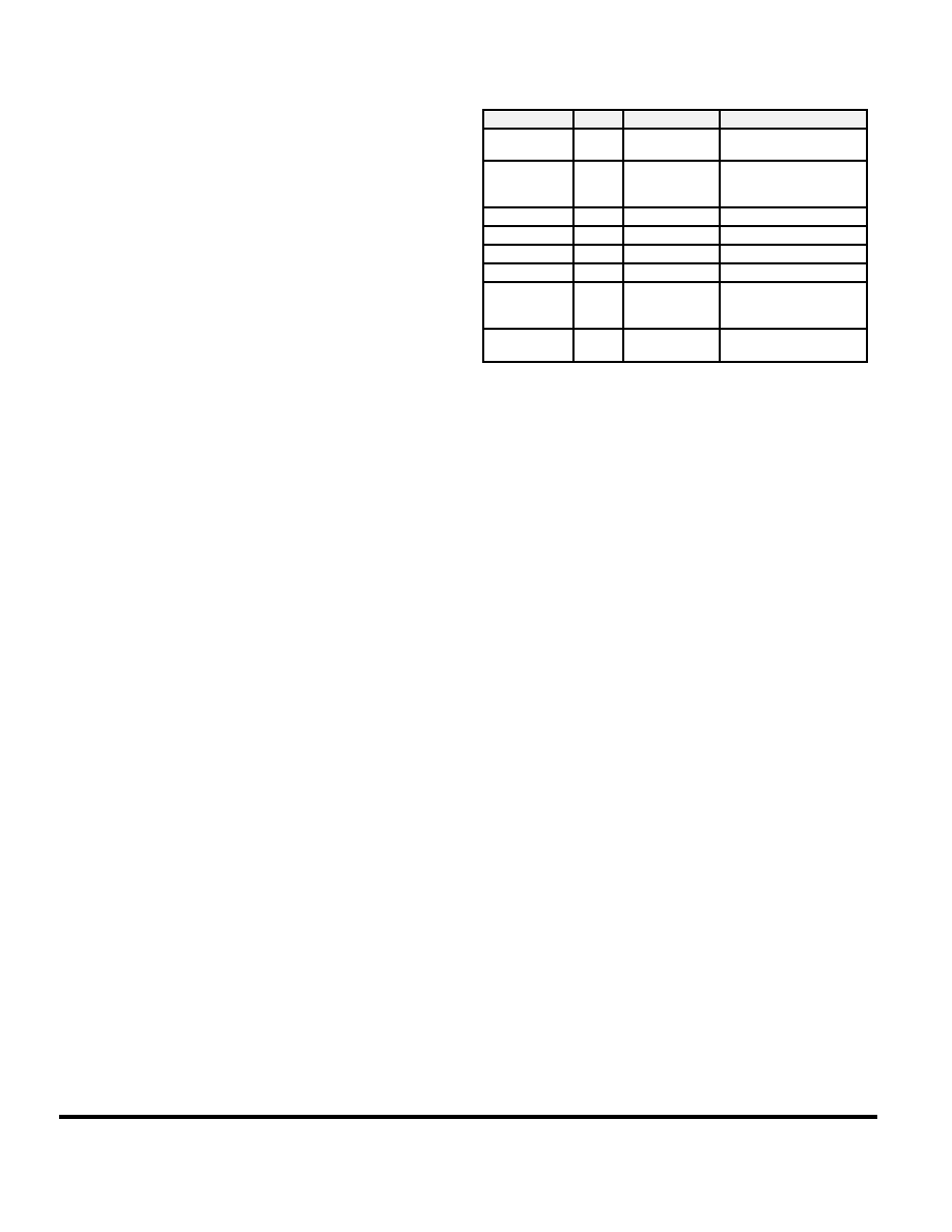
SERIAL INTERFACE
The STEL-9257 is configured by sending download
commands from an external PC over the serial
interface to a micro-processor, which in turn
configures the internal circuitry. The microprocessor
responds to each command by outputting a status
byte. The interface is a serial TTL interface that uses
industry standard UART timing at a baud rate of 19200
bps with 1 start bit, 8 data bits, 1 stop bit, and no parity
checking. To send a command to the microprocessor,
construct a data packet using the following format:
Field
Bytes
Range
Notes
STX
1
0x02
Start transmission
(value fixed)
Cmd ID
2
"00" to "2E"
ASCII
representation of
BCD hex value
Param 0
2
"00" to "FF"
Param 1
2
"00" to "FF"
Param 2
2
"00" to "FF"
Param 3
2
"00" to "FF"
Checksum
1
0x00 to 0xFF
Excludes STX,
checksum, and ETX
bytes
ETX
1
0x03
End transmission
(value fixed)
Refer to the Download Commands Section for
examples.
STEL-9257
26
Product Information
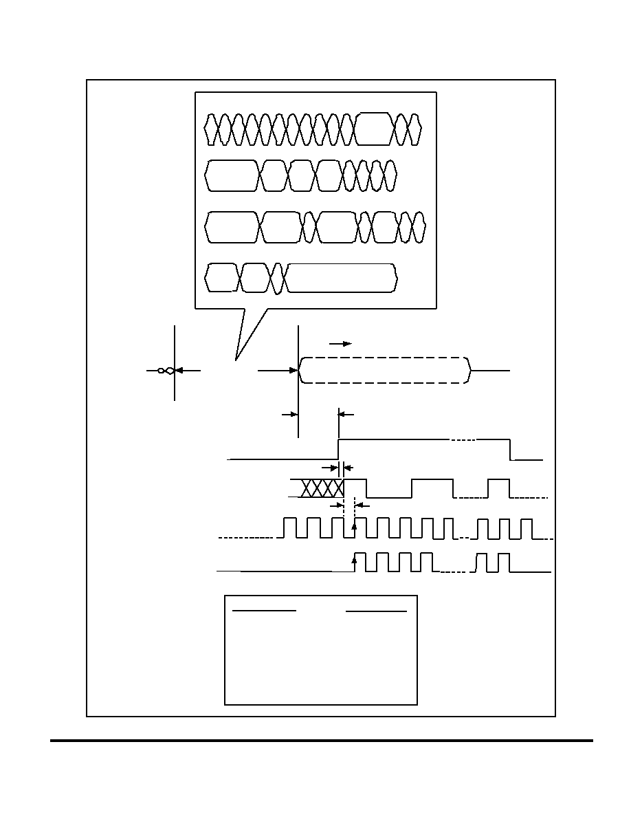
TIMING DIAGRAMS
1
1
DATA
Tx RF
DATA VALID/COLLISION*
DATA
GATED CLOCK OUT
CLOCK OUT (Continuous)
TPG 53450.c-10/29/97
1/2 BIT PERIOD
tdav SYMBOL PERIODS (see Table Below)
PREAMBLE
16 Symbol
14 Symbol
1
0
1
0
1
1
0
0
1
1
0
0
0
0
1
0
1
0
1
1
0
0
1
1
0
0
0
0
DAVIC
1
0
1
0
1
0
1
0
1
0
1
1
1
0
0
0
0
0
0
1
1
1
0
0
0
0
1
1
1
1
1
1
1
0
1
0
1
0
1
0
1
0
1
1
0
0
0
0
0
0
0
1
1
1
0
0
0
0
1
1
1
1
1
1
STEL-9244 PREAMBLE
1 1 1
0
0
0
0
0
0
0
0
0
0
ANY OF THE ABOVE PREAMBLES CAN BE SELECTED
1 1 1
0
0
0
0
0
0
0
0
0
0
4ns
Symbol Rate
0.128 -> 0.320 Msps
0.512 -> 0.772 Msps
1.024
1.28
1.544
2.048
2.56
tdav
39 symbols
40 symbols
41 symbols
42 symbols
43 symbols
44 symbols
45 symbols
Figure 12. Data Timing Diagram
Product Information
27
STEL-9257
WCP 52709.c-10/28/97
RF INPUT
DATA VALID
RSSI
ACCUMULATOR
CONTENTS
RSSI VALID
RSSI TYPE
RSSI DATA
SIGNAL 1
SIGNAL 2
SIGNAL 3
NOISE 3
NOISE 2
191 SYMBOLS
SIGNAL 1
SIGNAL 2
SIGNAL 3
NOISE 3
NOISE 2
PR
DATA BURST 1
PR
DATA BURST 3
NOISE 0
(ABORTED)
SIGNAL 1
NOISE 1
(ABORTED)
SIGNAL 2
NOISE 2
NOISE 3
NOISE 4
(INVALID)
SIGNAL 3
PR
DATA BURST 2
NOISE 5
(ABORTED)
NOISE 6
TRT SYMBOLS
1 SYMBOLS
*
TRT = 27 SYMBOLS FOR NH16 AND STEL 14 PREAMBLE, OR 35 SYMBOLS FOR DAVIC PREAMBLE
*
2 SYMBOLS
10 SYMBOLS
Figure 13. RSSI Timing Diagram*
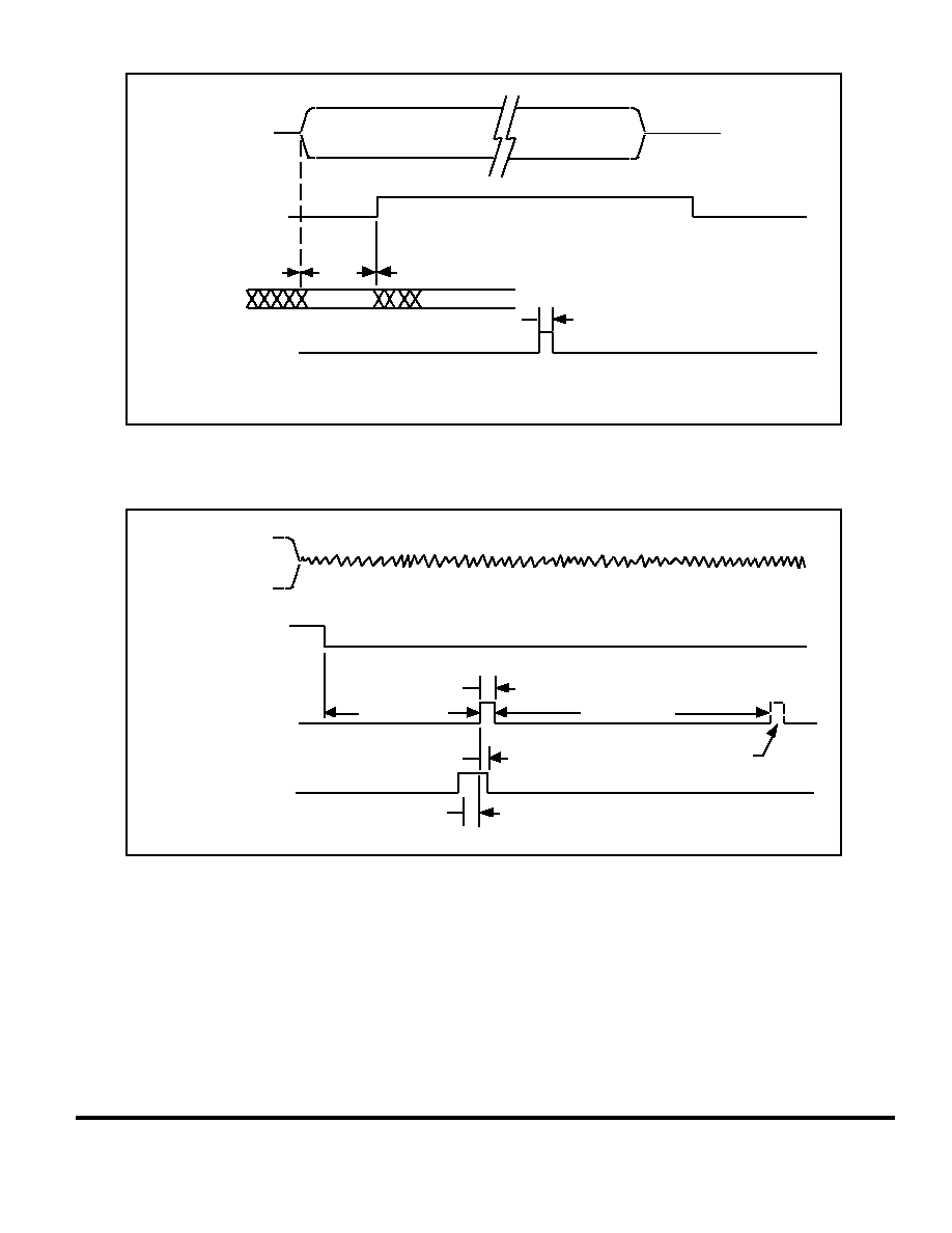
TPG 53472.c-10/24/97
DATA VALID
FREQ VALID
1 SYMBOL
FREQ DATA
1 SYMBOL UNKNOWN VALUE
Previous Value
185 Symbols
Next Value
Figure 14. Frequency Estimator Timing Diagram*
* Note: Jitter on all outputs signals is ± 40 ns.
STEL-9257
28
Product Information
TPG 53473.c-10/27/97
DATA VALID
thold = 0 ns
MODE 2,1,0
RSSI VALID
RF INPUT
*The Mode Pins should be stable before the burst arrives and should be held until Data Valid goes high.
The Mode Pins may be changed any time before the burst arrives, or after Data Valid goes high.
tsetup = 0 ns
1 S Y M B O L
*
Figure 15. Input Control Signals Timing Diagram
TPG 53680.c-10/28/97
DATA VALID
RSSI VALID
RF INPUT
NOISE HOLD
(Effective on next
noise measurement)
thold = 20 ns
tsetup = 50 ns
1 S Y M B O L
1 8 4 S Y M B O L S
1 9 3 S Y M B O L S
T h i s N o i s e M e a s u r e m e n t
i s i n h i b i t e d b y
N o i s e H o l d
Figure 16. Noise Hold Control Signals Timing Diagram

WCP 970050
Copyright © Intel Corporation, December 15, 1999.
All rights reserved
Information in this document is provided in connection with
IntelÆ products. No license, express or implied, by estoppel
or otherwise, to any intellectual property rights is granted by
this document. Except as provided in Intels Terms and Con-
ditions of Sale for such products, Intel assumes no liability
whatsoever, and Intel disclaims any express or implied
warranty, relating to sale and/or use of IntelÆ products in-
cluding liability or warranties relating to fitness for a particu-
lar purpose, merchantability, or infringement of any patent,
copyright or other intellectual property right. Intel products
are not intended for use in medical, life saving, or life sus-
taining applications.
Intel may make changes to specifications and product de-
scriptions at any time, without notice.
For Further Information Call or Write
INTEL CORPORATION
Cable Network Operation
350 E. Plumeria Drive, San Jose, CA 95134
Customer Service Telephone: (408) 545-9700
Technical Support Telephone: (408) 545-9799
FAX: (408) 545-9888