
Other brands and names are the property of their respective owners
Information in this document is provided in connection with Intel products Intel assumes no liability whatsoever including infringement of any patent or
copyright for sale and use of Intel products except as provided in Intel's Terms and Conditions of Sale for such products Intel retains the right to make
changes to these specifications at any time without notice Microcomputer Products may have minor variations to this specification known as errata
November 1994
COPYRIGHT
INTEL CORPORATION 1996
Order Number 231428-006
UPI-452
CHMOS PROGRAMMABLE I O PROCESSOR
83C452 - 8K
c
8 Mask Programmable Internal ROM
80C452 - External ROM EPROM
Y
83C452 80C452 3 5 to 14 MHz Clock
Rate
Y
Software Compatible with the MCS-51
Family
Y
128-Byte Bi-Directional FIFO Slave
Interface
Y
Two DMA Channels
Y
256
c
8-Bit Internal RAM
Y
34 Additional Special Function
Registers
Y
40 Programmable I O Lines
Y
Two 16-Bit Timer Counters
Y
Boolean Processor
Y
Bit Addressable RAM
Y
8 Interrupt Sources
Y
Programmable Full Duplex Serial
Channel
Y
64K Program Memory Space
Y
64K Data Memory Space
Y
68-Pin PGA and PLCC
(See Packaging Spec Order
231369)
The Intel UPI-452 (Universal Peripheral Interface) is a 68 pin CHMOS Slave I O Processor with a sophisticated
bi-directional FIFO buffer interface on the slave bus and a two channel DMA processor on-chip The UPI-452
is the newest member of Intel's UPI family of products It is a general-purpose slave I O Processor that allows
the designer to grow a customized interface solution
The UPI-452 contains a complete 80C51 with twice the on-chip data and program memory The sophisticated
slave FIFO module acts as a buffer between the UPI-452 internal CPU and the external host CPU To both the
external host and the internal CPU the FIFO module looks like a bi-directional bottomless buffer that can both
read and write data The FIFO manages the transfer of data independent of the UPI-452 core CPU and
generates an interrupt or DMA request to either CPU host or internal as a FIFO service request
The FIFO consists of two channels the Input FIFO and the Output FIFO The division of the FIFO module
array 128 bytes between Input channel and Output channel is programmable by the user Each FIFO byte
has an additional logical ninth bit to distinguish between a data byte and a Data Stream Command byte
Additionally Immediate Commands allow direct interrupt driven bi-directional communication between the
UPI-452 internal CPU and external host CPU bypassing the FIFO
The on-chip DMA processor allows high speed data transfers from one writeable memory space to another
As many as 64K bytes can be transferred in a single DMA operation Three distinct memory spaces may be
used in DMA operations Internal Data Memory External Data Memory and the Special Function Registers
(including the FIFO IN FIFO OUT and Serial Channel Special Functions Registers)

UPI-452
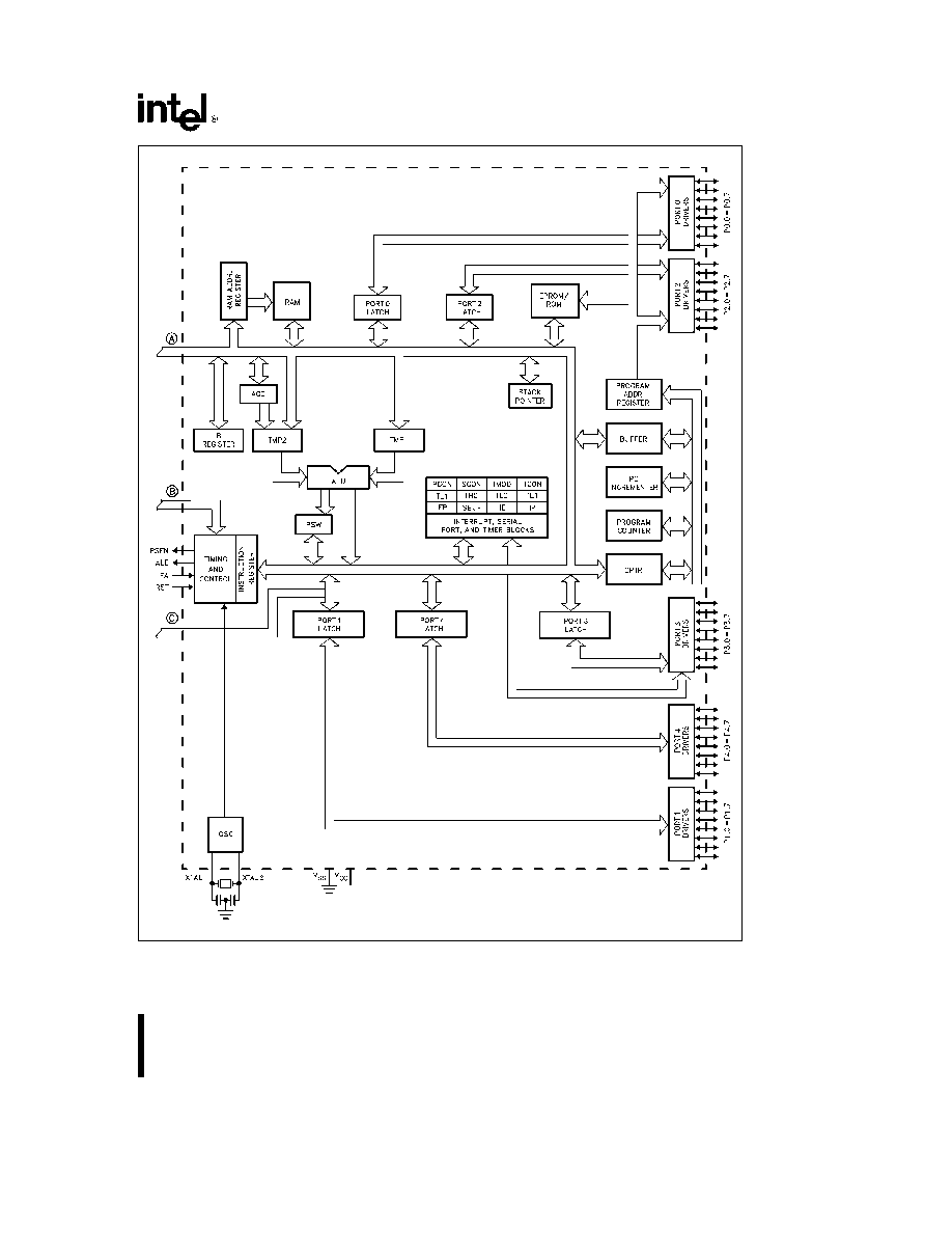
231428 � 1
Figure 1 Architectural Block Diagram
2
UPI-452
231428 � 2
Figure 1 Architectural Block Diagram
(Continued)
3

UPI-452
TABLE OF CONTENTS
CONTENTS
PAGE
Introduction
1
Table of Contents
4
List of Tables and Figures
5
Pin Description
7
Architectural Overview
10
Introduction
10
FIFO Buffer Interface
10
FIFO Programmable Features
11
Immediate Commands
12
DMA
12
FIFO Slave Interface Functional Description
12
Overview
12
Input FIFO Channel
13
Output FIFO Channel
14
Immediate Commands
16
Host
Slave Interface Special Function Registers
18
Slave Interface Special Function Registers
18
External Host Interface Special Function Registers
20
FIFO Module
External Host Interface
22
Overview
22
Slave Interface Address Decoding
22
Interrupts to the Host
22
DMA Requests to the Host
24
FIFO Module
Internal CPU Interface
24
Overview
24
Internal CPU Access to FIFO via Software Instructions
24
General Purpose DMA Channels
25
Overview
25
Architecture
25
DMA Special Function Registers
26
DMA Transfer Modes
27
External Memory DMA
29
Latency
29
DMA Interrupt Vectors
29
Interrupts When DMA is Active
30
DMA Arbitration
30
Interrupts
32
Overview
32
FIFO Module Interrupts to Internal CPU
32
Interrupt Enabling and Priority
33
FIFO
External Host Interface FIFO DMA Freeze Mode
35
Overview
35
Initialization
35
Invoking FIFO DMA Freeze Mode During Normal Operation
36
FIFO Module Special Function Register Operation During FIFO DMA Freeze Mode
37
Internal CPU Read
Write of the FIFO During FIFO DMA Freeze Mode
41
Memory Organization
41
Accessing External Memory
41
Miscellaneous Special Function Register Descriptions
43
4

UPI-452
LIST OF TABLES AND FIGURES
Figures
1
Architectural Block Diagram
2
2
UPI 452 68-Pin PLCC Pinout Diagram
6
3
UPI-452 Conceptual Block Diagram
10
4
UPI-452 Functional Block Diagram
11
5
Input FIFO Channel Functional Block Diagram
13
6
Output FIFO Channel Functional Block Diagram
15
7a Handshake Mechanisms for Handling Immediate Command IN Flowchart
17
7b Handshake Mechanisms for Handling Immediate Command OUT Flowchart
17
8
DMA Transfer from External to External Memory
31
9
DMA Transfer from External to Internal Memory
31
10
DMA Transfer from Internal to External Memory
31
11
DMA Transfer Waveform Internal to Internal Memory
32
12
Disabling FIFO to Host Slave Interface Timing Diagram
36
Tables
1
Input FIFO Channel Registers
13
2
Output FIFO Channel Registers
15
3
UPI-452 Address Decoding
23
4
DMA Accessible Special Function Registers
26
5
DMA Mode Control - PCON SFR
29
6
Interrupt Priority
32
7
Interrupt Vector Addresses
32
8
Slave Bus Interface Status During FIFO DMA Freeze Mode
35
9
FIFO SFR's Characteristics During FIFO DMA Freeze Mode
38
10
Threshold SFRs Range of Values and Number of Bytes to be Transferred
39
11a Internal Memory Addressing
41
11b 80C51 Special Function Registers
42
11c UPI-452 Additional Special Function Registers
42
12
Program Status Word (PSW)
44
13
PCON Special Function Register
44
5

UPI-452
P C Board View
As Viewed from the Component Side of the P C Board
(Underside of Socket)
231428 � 32
Figure 2 UPI 452 68-Pin PLCC Pinout Diagram
6
UPI-452
UPI MICROCONTROLLER FAMILY
The UPI-452 joins the current members of the UPI
microcontroller family UPI's are derivatives of the
MCS
TM
family of microcontrollers Because of their
on-chip system bus interface UPI's are designed to
be system bus ``slaves'' while their microcontroller
counterparts are intended as system bus ``masters''
These UPI Microcontrollers are fully supported by
Intel's development tools (ICE ASM and PLM)
Packaging
The 80C452 83C452 is available in a 68-pin PLCC
package
UPI Family
MCS Family
RAM
ROM
(Slave
(Master
Speed
(Bytes)
(Bytes)
Configuration)
Configuration)
80C452
80C51
12 MHz
256
83C452
80C51
12 MHz
256
8K
80C452-1
80C51
14 MHz
256
83C452-1
80C51
14 MHz
256
8K
UPI-452 PIN DESCRIPTIONS
Symbol
Pin
Type
Name and Function
V
SS
9 43
I
Circuit Ground
V
CC
60
I
a
5V power supply during normal and idle mode operation It is also
the standby power pin for power down mode
XTAL1
38
I
Input to the oscillator's high gain amplifier A crystal or external
source can be used
XTAL2
39
O
Output from the high gain amplifier
Port 0
I O
Port 0 is an 8-bit open drain bi-directional I O port Port 0 can sink
(AD0 � AD7)
eight LS TTL inputs It is also the multiplexed low-order address and
P0 0
8
data local expansion bus during accesses to external memory
1
10
2
11
3
12
4
13
5
14
6
15
P0 7
16
7
UPI-452
UPI-452 PIN DESCRIPTIONS
(Continued)
Symbol
Pin
Type
Name and Function
Port 1
I O
Port 1 is an 8-bit quasi-bi-directional I O port Port 1 can sink four
(A0 � A7)
LS TTL inputs The alternate functions can only be activated if the
(HLD HLDA)
corresponding bit latch in the port SFR contains a 1 Otherwise the
P1 0
7
port pin is stuck at 0 Pins P1 5 and P1 6 are multiplexed with HLD
and HLDA respectively whose functions are defined as below
1
6
Port Pin
Alternate Function
2
5
P1 5
HLD
Local bus hold
3
4
input output signal
4
3
P1 6
HLDA
Local bus hold
5
2
acknowledge input
6
1
P1 7
68
Port 2
I O
Port 2 is an 8-bit quasi-bi-directional I O port It also emits the high-
(A8 � A15)
order 8 bits of address when accessing local expansion bus
P2 0
29
external memory Port 2 can sink four LS TTL inputs
1
28
2
27
3
25
4
24
5
23
6
22
7
21
Port 3
I O
Port 3 is an 8-bit quasi-bi-directional I O port It is also multiplexed
P3 0
67
with the interrupt timer local serial channel RD and WR
1
66
functions that are used by various options The alternate functions
2
65
can only be activated if the corresponding bit latch in the port SFR
3
64
contains a 1 Otherwise the port pin is stuck at 0 Port 3 can sink
4
63
four LS TTL inputs The alternate functions assigned to the pins of
5
62
Port 3 are as follows
6
61
Port Pin
Alternate Function
P3 7
59
P3 0
RxD
Serial input port
P3 1
TxD
Serial output port
P3 2
INT0
Interrupt 0 Input
P3 3
INT1
Interrupt 1 Input
P3 4
T0
Input to counter 0
P3 5
T1
Input to counter 1
P3 6
WR
The write control signal latches the
data from Port 0 outputs into the
External Data Memory on the
local bus
P3 7
RD
The read control signal latches the
data from Port 0 outputs on the
local bus
8

UPI-452
UPI-452 PIN DESCRIPTIONS
(Continued)
Symbol
Pin
Type
Name and Function
Port 4
I O
Port 4 is an 8-bit quasi-bi-directional I O port Port 4 can sink
P4 0
30
source four TTL inputs
1
2
32
3
33
4
34
5
35
6
36
7
37
RST
20
I
A high level on this pin for two machine cycles while the oscillator is
running resets the device An internal pulldown resistor permits
Power-on reset using only a capacitor connected to V
CC
This pin does not receive the power down voltage as is the case for
HMOS MCS-51 family members This function has been transferred
to the V
CC
pin
ALE
18
O
Provides Address Latch Enable output used for latching the
address into external memory during normal operation ALE can
sink source eight LS TTL inputs
PSEN
19
O
The Program Store Enable output is a control signal that enables
the external Program Memory to the bus during normal fetch
operation PSEN can sink source eight LS TTL inputs
EA
17
I
When held at TTL high level the UPI-452 executes instructions
from the internal ROM when the PC is less than 8192 (8K 2000H)
When held at a TTL low level the UPI-452 fetches all instructions
from external Program Memory
DB0
58
I O
Host Bus Interface is an 8-bit bi-directional bus It is used to transfer
DB1
57
data and commands between the UPI-452 and the host processor
DB2
56
This bus can sink source eight LS TTL inputs
DB3
55
DB4
54
DB5
53
DB6
52
DB7
51
CS
44
I
This pin is the Chip Select of the UPI-452
A0
40
I
These three address lines are used to interface with the host
A1
41
system They define the UPI-452 operations The interface is
A2
42
compatible with the Intel microprocessors and the MULTIBUS
READ
46
I
This pin is the read strobe from the host CPU Activating this pin
causes the UPI-452 to place the contents of the Output FIFO (either
a command or data) or the Host Status Control Special Function
Register on the Slave Data Bus
WRITE
47
I
This pin is the write strobe from the host Activating this pin will
cause the value on the Slave Data Bus to be written into the register
specified by A0 � A2
DRQIN
49
O
This pin requests an input transfer from the host system whenever
INTRQIN
the Input Channel requires data
DRQOUT
48
O
This output pin requests an output transfer whenever the Output
INTRQOUT
Channel requires service If the external host to UPI-452 DMA is
enabled and a Data Stream Command is at the Output FIFO
DRQOUT is deactivated and INTRQ is activated (see `GENERAL
PURPOSE DMA CHANNELS' section)
9

UPI-452
UPI-452 PIN DESCRIPTIONS
(Continued)
Symbol
Pin
Type
Name and Function
INTRQ
50
O
This output pin is used to interrupt the host processor when an
Immediate Command Out or an error condition is encountered It is
also used to interrupt the host processor when the FIFO requests
service if the DMA is disabled and INTRQIN and INTRQOUT are
not used
DACK
45
I
This pin is the DMA acknowledge for the host bus interface Input
and Output Channels When activated a write command will cause
the data on the Slave Data Bus to be written as data to the Input
Channel (to the Input FIFO) A read command will cause the Output
Channel to output data (from the Output FIFO) on to the Slave Data
Bus This pin should be driven high (a5V) in systems which do not
have a DMA controller (see Address Decoding)
V
CC
26
I
a
5V power supply during operation
ARCHITECTURAL OVERVIEW
Introduction
The UPI-452 slave microcontroller incorporates an
80C51 with double the program and data memory a
slave interface which allows it to be connected di-
rectly to the host system bus as a peripheral a FIFO
buffer module a two channel DMA processor and a
fifth I O port (Figure 3) The UPI-452 retains all of
the 80C51 architecture and is fully compatible with
the MCS-51 instruction set
The Special Function Register (SFR) interface con-
cept introduced in the MCS-51 family of microcon-
trollers has been expanded in the UPI-452 To the
20 Special Function Registers of the MCS-51 the
UPI-452 adds 34 more These additional Special
Function Registers like those of the MCS-51 pro-
vide access to the UPI-452 functional elements in-
cluding the FIFO DMA and added interrupt capabili-
ties Several of the 80C51 core Special Function
Registers have also been expanded to support add-
ed features of the UPI-452
This data sheet describes the unique features of the
UPI-452 Refer to the 80C51 data sheet for a de-
scription of the UPI-452's core CPU functional
blocks including
Timers Counters
I O Ports
Interrupt timing and control (other than FIFO and
DMA interrupts)
Serial Channel
Local Expansion Bus
Program Data Memory structure
Power-Saving Modes of Operation
CHMOS Features
Instruction Set
Figure 3 contains a conceptual block diagram of the
UPI-452 Figure 4 provides a functional block dia-
gram
FIFO Buffer Interface
A unique feature of the UPI-452 is the incorporation
of a 128 byte FIFO array at the host-slave interface
The FIFO allows asynchronous bi-directional trans-
fers between the host CPU and the internal CPU
231428 � 7
Figure 3 UPI-452 Conceptual Block Diagram
10

UPI-452
231428 � 8
Figure 4 UPI-452 Functional Block Diagram
The division of the 128 bytes between Input and
Output channels is user programmable allowing
maximum flexibility If the entire 128 byte FIFO is
allocated to the Input channel a high performance
Host can transfer up to 128 bytes at one time then
dedicate its resources to other functions while the
internal CPU processes the data in the FIFO Vari-
ous handshake signals allow the external Host to
operate independently and without frequent monitor-
ing of the UPI-452 internal CPU The FIFO Buffer
insures that the slave processor receives data in the
same order that it was sent by the host without the
need to keep track of addresses Three slave bus
interface handshake methods are supported by the
UPI-452 DMA Interrupt and Polled
The FIFO is nine bits wide The ninth bit acts as a
command data flag Commands written to the FIFO
by either the host or internal CPU are called Data
Stream Commands or DSCs DSCs are written to
the input FIFO by the Host via a unique external
address DSCs are written to the output FIFO by the
internal CPU via the COMMAND OUT Special Func-
tion Register (SFR) When encountered by the host
or internal CPU a Data Stream Command can be
used as an address vector to user defined service
routines DSCs provide synchronization of data and
commands between the Host and internal CPU
FIFO PROGRAMMABLE FEATURES
Size of Input Output Channels
The 128 bytes of FIFO space can be allocated be-
tween the Input and Output channels via the Chan-
nel Boundary Pointer (CBP) SFR This register con-
tains the number of address locations assigned to
the Input channel The remaining address locations
are automatically assigned to the Output FIFO The
CBP SFR can only be programmed by the internal
CPU during FIFO DMA Freeze Mode (See FIFO-Ex-
ternal Host Interface FIFO DMA Freeze Mode de-
scription) The CBP is initialized to 40H (64 bytes)
upon reset
The number in the Channel Boundary Pointer SFR is
actually the first address location of the Output
FIFO Writing to the CBP SFR reassigns the Input
and Output FIFO address space Whenever the CBP
is written the Input FIFO pointers are reset to zero
and the Output FIFO pointers are set to the value in
the CBP SFR
All of the FIFO space may be assigned to one chan-
nel In such a situation the other channel's data path
consists of a single SFR (FIFO IN COMMAND IN or
FIFO OUT COMMAND OUT SFR) location
CBP
Input FIFO
Output FIFO
Register
Size
Size
0
1
128
1
1
128
2
2
126
3
3
125
4
4
124
7B
123
5
7C
124
4
7D
125
3
7E
128
1
7F
128
1
11

UPI-452
FIFO Read Write Pointers
These normally operate in auto-increment (and auto-
rollover) mode but can be reassigned by the internal
CPU during FIFO DMA Freeze Mode (See FIFO-Ex-
ternal Host Interface FIFO DMA Freeze Mode de-
scription)
Threshold Register
The Input FIFO Threshold SFR contains the number
of empty bytes that must be available in the Input
FIFO to generate a Host interrupt The Output FIFO
Threshold SFR contains the number of bytes data
and or DSC(s) that must be in the FIFO before an
interrupt is generated The Threshold feature pre-
vents the Host from being interrupted each time the
FIFO needs to load or unload one byte of data The
thresholds therefore allow the FIFO's operation to
be adjusted to the speed of the Host optimizing the
overall interface performance
NOTE
DSC's should be allowed to be written into the out-
put FIFO by the UPI-452 code only when the serv-
ice request is law The service request can be mon-
itored by b7 of OTHR This guideline will elimate
the possibility of a DSC being written to the output
FIFO with the intention of setting the service re-
quest while having the number of bytes in the out-
put FIFO below the threshold This condition can
occur if the FIFO contains at least two bytes the
service request is being asserted and the host
reads from the output FIFO until one byte remains
Immediate Commands
The UPI-452 provides in addition to data and DSCs
a third direct means of communication between the
external Host and internal CPU called Immediate
Commands As the name implies an Immediate
Command is available to the receiving CPU immedi-
ately via an interrupt without being entered into the
FIFO as are Data Stream Commands Like Data
Stream Commands Immediate Commands are writ-
ten either via a unique external address by the host
CPU or via dedicated SFR by the internal CPU
The DSC and or Immediate Command interface
may be defined as either Interrupt or Polled under
user program control via the Interrupt Enable (IE)
Slave Control Register (SLCON) and Interrupt En-
able Priority (IEP) Special Function Registers for the
internal CPU and via the Host Control SFR for the
external Host CPU
DMA
The UPI-452 contains a two channel internal DMA
controller which allows transfer of data between any
of the three writeable memory spaces Internal Data
Memory External Load Expansion Bus Data Memo-
ry and the Special Function Register array The Spe-
cial Function Register array appears as a set of
unique dedicated memory addresses which may be
used as either the source or destination address of a
DMA transfer Each DMA channel is independently
programmable via dedicated Special Function Reg-
isters for mode source and destination addresses
and byte count to be transferred Each DMA channel
has four programmable modes
Alternate Cycle Mode
Burst Mode
FIFO or Serial Channel Demand Mode
External Demand Mode
A complete description of each mode and DMA op-
eration may be found in the section titled ``General
Purpose DMA Channels''
FIFO SLAVE INTERFACE
FUNCTIONAL DESCRIPTION
Overview
The FIFO is a 128 Byte RAM array with recirculating
pointers to manage the read and write accesses
The FIFO consists of an Input and an Output chan-
nel Access cycles to the FIFO by the internal CPU
and external Host are interleaved and appear to be
occurring concurrently to both the internal CPU and
external Host Interleaving access cycles ensures
efficient use of this shared resource The internal
CPU accesses the FIFO in the same way it would
access any of the Special Function Registers e g
direct and register indirect addressing as well as ar-
ithmetric and logical instructions
12
UPI-452
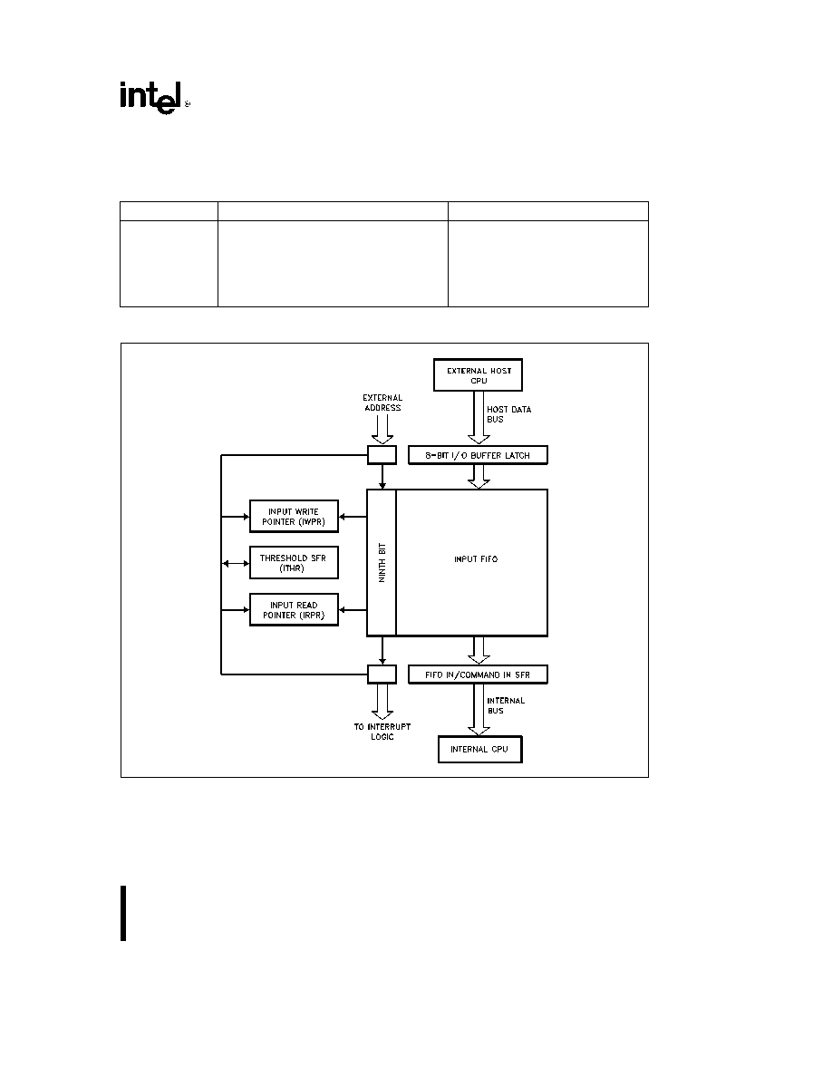
Input FIFO Channel
The Input FIFO Channel provides for data transfer from the external Host to the internal CPU (Figure 5) The
registers associated with the Input Channel during normal operation are listed in Table 1
Table 1 Input FIFO Channel Registers
Register Name
Description
1)
Input Buffer Latch
Host CPU Write only
2)
FIFO IN SFR
Internal CPU Read only
3)
COMMAND IN SFR
Internal CPU Read only
4)
Input FIFO Read Pointer SFR
Internal CPU Read only
5)
Input FIFO Write Pointer SFR
Internal CPU Read only
6)
Input FIFO Threshold SFR
Internal CPU Read only
See ``FIFO-EXTERNAL HOST INTERFACE FIFO DMA FREEZE MODE'' section for FIFO DMA Freeze Mode SFR characteristics description
231428 � 9
Figure 5 Input FIFO Channel Functional Block Diagram
13

UPI-452
The host CPU writes data and Data Stream Com-
mands into the Input Buffer Latch on the rising edge
of the external WR signal External addressing de-
termines whether the byte is a data byte or Data
Stream Command and the FIFO logic sets the ninth
bit of the FIFO accordingly as the byte is moved
from the Input Buffer Latch into the FIFO A ``1'' in
the ninth bit indicates that the incoming byte is a
Data Stream Command The internal CPU reads
data bytes via the FIFO IN SFR and Data Stream
Commands via the COMMAND IN SFR
A Data Stream Command will generate an interrupt
to the internal CPU prior to being read and after
completion of the previous operation The DSC can
then be read via the COMMAND IN SFR Data can
only be read via the FIFO IN SFR and Data Stream
Commands via the COMMAND IN SFR Attempting
to read Data Stream Commands as data by address-
ing the FIFO IN SFR will result in ``0FFH'' being
read and the Input FIFO Read Pointer will remain
intact (This prevents accidental misreading of Data
Stream Commands ) Attempting to read data as
Data Stream Commands will have the same conse-
quence
The Input FIFO Channel addressing is controlled by
the Input FIFO Read and Write Pointer SFRs These
SFRs are read only registers during normal opera-
tion However during FIFO DMA Freeze Mode (See
FIFO-External Host Interface FIFO DMA Freeze
Mode description) the internal CPU has write ac-
cess to them Any write to these registers in normal
mode will have no effect The Input Write Pointer
SFR contains the address location to which data
commands are written from the Input Buffer Latch
The write pointer is automatically incremented after
each write and is reset to zero if equal to the CBP
as the Input FIFO operates as a circular buffer
If a write is performed on an empty FIFO the first
byte is also written into the FIFO IN or COMMAND
IN SFR If the Host continues writing while the Input
FIFO is full an external interrupt if enabled is sent
to the host to signal the overrun condition The
writes are ignored by the FIFO control logic Similar-
ly an internal CPU read of an empty FIFO will cause
an underrun error interrupt to be generated to the
internal CPU and a value of ``0FFH'' will be read by
the internal CPU
The Read Pointer SFR holds the address of the next
byte to be read from the Input FIFO An Input FIFO
read operation post-increments the Input Read
Pointer SFR and loads a new data byte into the
FIFO IN SFR or a Data Stream Command into the
COMMAND IN SFR at the end of the read cycle
An Input FIFO Request for Service (via DMA Inter-
rupt or a flag) is generated to the Host whenever
more data can be written into the Input FIFO For
efficient utilization of the Host a ``threshold'' value
can be programmed into the Input FIFO Threshold
SFR The range of values of the Input FIFO Thresh-
old SFR can be from 0 to (CBP-3) The Request for
Service Interrupt is generated only after the Input
FIFO has room to accommodate a threshold number
of bytes or more The threshold is equal to the total
number of bytes assigned to the Input FIFO (CBP)
minus the number of bytes programmed in the Input
FIFO Threshold SFR With this feature the Host is
assured that it can write at least a threshold number
of bytes to the Input FIFO channel without worrying
about an overrun condition Once the Request for
Service is generated it remains active until the Input
FIFO becomes full
Output FIFO Channel
The Output FIFO Channel provides data transfer
from the UPI-452 internal CPU to the external Host
(Figure 6)
The registers associated with the Output Channel
during normal operation are listed in Table 2
14

UPI-452
231428 � 10
Figure 6 Output FIFO Channel Functional Block Diagram
Table 2 Output FIFO Channel Registers
Register Name
Description
1)
Output Buffer Latch
Host CPU Read only
2)
FIFO OUT SFR
Internal CPU Read and Write
3)
COMMAND OUT SFR
Internal CPU Read and Write
4)
Output FIFO Read Pointer SFR
Internal CPU Read only
5)
Output FIFO Write Pointer SFR
Internal CPU Read only
6)
Output FIFO Threshold SFR
Internal CPU Read only
See ``FIFO-EXTERNAL HOST INTERFACE FIFO DMA FREEZE MODE'' section for FIFO DMA Freeze Mode register characteristics description
15

UPI-452
The UPI-452 internal CPU transfers data to the Out-
put FIFO via the FIFO OUT SFR and commands via
the COMMAND OUT SFR If the byte is written to
the COMMAND OUT SFR the ninth bit is automati-
cally set (e1) to indicate a Data Stream Command
If the byte is written to the FIFO OUT SFR the ninth
bit is cleared (e0) Thus the FIFO OUT and COM-
MAND OUT SFRs are the same but the address de-
termines whether the byte entered in the FIFO is a
DSC or data byte
The Output FIFO preloads a byte into the Output
Buffer Latch When the Host issues a RD
signal
the data is immediately read from the Output Buffer
Latch The next data byte is then loaded into the
Output Buffer Latch a flag is set and an interrupt if
enabled is generated if the byte is a DSC (ninth bit
is set) The operation is carefully timed such that an
interrupt can be generated in time for it to be recog-
nized by the Host before its next read instruction
Internal CPU write and external Host read opera-
tions are interleaved at the FIFO so that they appear
to be occurring concurrently
The Output FIFO read and write pointer operation is
the same as for the Input Channel Writing to the
FIFO OUT or COMMAND OUT SFRs will increment
the Output Write Pointer SFR but reading from it will
leave the write pointer unchanged A rollover of the
Output FIFO Write Pointer causes the pointer to be
reset to the value in the Channel Boundary Pointer
(CBP) SFR
If the external host attempts to read a Data Stream
Command as a data byte it will result in invalid data
(0FFH) being read The DSC is not lost because the
invalid read does not increment the pointer Similarly
attempting to read a data byte as a Data Stream
Command has the same result
A Request for Service is generated to the external
Host under the following two conditions
1 ) Whenever the internal CPU has written a thresh-
old number of bytes or more into the Output FIFO
(threshold e (OTHR) a 1) The threshold num-
ber should be chosen such that the bus latency
time for the external Host does not result in a
FIFO overrun error condition on the internal CPU
side The threshold limit should be large enough
to make a bus request by the UPI-452 to the ex-
ternal host CPU worthwhile Once a request for
service is generated the request remains active
until the Output FIFO becomes empty The range
of values of the FIFO Output Threshold (OTHR)
SFR is from 2 to (80H-CBP)-1
The threshold
number can be programmed via the OTHR SFR
2 ) The second type of Request for Service is called
``Flush Mode'' and occurs when the internal CPU
writes a Data Stream Command into the Output
FIFO Its purpose is to ensure that a data block
entered into the Output FIFO which is less than
the programmed threshold will generate a Re-
quest for Service interrupt if enabled and be
read or ``Flushed'' from the Output FIFO by the
external host CPU regardless of the status of the
OTHR SFR
NOTE
The host port read or write strobe (TPW) should be
limited to a maximum of 4 TCLCL This guideline
will eliminate a potential output FIFO Request lock-
up from occurring if the host reads the last byte
from the output FIFO while the UPI-452 is begin-
ning to write another byte to the output FIFO
Immediate Commands
Immediate Commands provide direct communica-
tion between the external Host and UPI-452 Unlike
Data Stream Commands which are entered into the
FIFO the Immediate Command is available to the
receiving CPU directly bypassing the FIFO The Im-
mediate Command can serve as a program vector
pointing into a jump table in the recipients software
Immediate Command Interrupts are generated if en-
abled and a bit in the appropriate Status Register is
set when an Immediate Command is input or output
A similar bit is provided to acknowledge when an
Immediate Command has been read and whether
the register is available to receive another com-
mand The bits are reset when the Immediate Com-
mands are read Two Special Function Registers are
dedicated to the Immediate Command interface Ex-
ternal addressing determines whether the Host is
accessing the Input FIFO or the Immediate Com-
mand IN (IMIN) SFR The internal CPU writes Imme-
diate Commands to the Immediate Command OUT
(IMOUT) SFR
Both processors have the ability to enable or disable
Immediate Command Interrupts By disabling the in-
terrupt the recipient of the Immediate Command
can poll the status SFR and read the Immediate
Command at its convenience
Immediate Com-
mands should only be written when the appropriate
Immediate Command SFR is empty (as indicated in
the appropriate status SFR HSTAT SSTAT) Simi-
larly the Immediate Command SFR should only be
read when there is data in the Register
The flowcharts in Figure 7a and 7b illustrate the
proper handshake mechanisms between the exter-
nal Host and internal CPU when handling Immediate
Commands
16
UPI-452
231428 � 11
Figure 7a Handshake Mechanisms for Handling
Immediate Command IN Flowchart
231428 � 12
Figure 7b Handshake Mechanisms for Handling
Immediate Command OUT Flowchart
17
UPI-452
HOST
SLAVE INTERFACE SPECIAL FUNCTION REGISTERS
Slave Interface Special Function Registers
The Internal CPU interfaces with the FIFO slave module via the following registers
1) Mode Special Function Register (MODE)
2) Slave Control Special Function Register (SLCON)
3) Slave Status Special Function Register (SSTAT)
Each register resides in the SFR Array and is accessible via all direct addressing modes except bit Only the
Slave Control Register (SLCON) is bit addressable
1) MODE Special Function Register (MODE)
The MODE SFR provides the primary control of the external host-FIFO interface It is included in the SFR
Array so that the internal CPU can configure the external host-FIFO interface should the user decide that the
UPI-452 slave initialize itself independent of the external host CPU
The MODE SFR can be directly modified by the internal CPU through direct address instructions It can also be
indirectly modified by the external host CPU by setting up a MODE SFR service routine in the UPI-452 program
memory and having the host issue a Command either Immediate or DSC to vector to that routine
Symbolic
Physical
Address
Address
MODE
MD6
MD5
MD4
0F9H
(MSB)
(LSB)
Status On Reset
1
0
0
0
1
1
1
1
MD7
(reserved)
MD6
Request for Service to external CPU via
1 e DMA (DRQIN DRQOUT) request to external host when the Input or Output FIFO channel re-
quests service
0 e Interrupt (INTRQIN INTRQOUT or INTRQ) to external host when the Input or Output FIFO
channel requests service or a DSC is encountered in the I O Buffer Latch
MD5
Configure DRQIN INTRQIN and DRQOUT INTRQOUT to be either
1 e Enable (Actively driven)
0 e Disable (Tri-state)
MD4
Configure INTRQ to be either
1 e Enable (Actively driven)
0 e Disable (Tri-state)
MD3
(reserved)
MD2
(reserved)
MD1
(reserved)
MD0
(reserved)
2) Slave Control SFR (SLCON)
The Slave Control SFR is used to configure the FIFO-internal CPU interface All interrupts are to the internal
CPU
18

UPI-452
Symbolic
Physical
Address
Address
SLCON
IFI
OFI
ICII
ICOI
FRZ
IFRS
OFRS
0E8H
(MSB)
(LSB)
Status On Reset
0
0
0
0
0
1
0
0
IFI
Enable Input FIFO Interrupt (due to Underrun Error Condition Data Stream Command or Request
Service)
1 e Enable
0 e Disable
OFI
Enable Output FIFO Interrupt (due to Overrun Error Condition or Request Service)
1 e Enable
0 e Disable
Note If the DMA is configured to service a FIFO demand then the Request for Service Interrupt is
not generated
ICII
Generate Interrupt when a command is written to the Immediate Command in Register
1 e Enable
0 e Disable
ICOI
Generate Interrupt when Immediate Command Out Register is Available
1 e Enable
0 e Disable
FRZ
Enable FIFO DMA Freeze Mode
1 e Normal operation
0 e FIFO DMA Freeze Mode
SC2
(reserved)
IFRS
Input FIFO Channel Request for Service
1 e Request when Input FIFO not empty
0 e Request when Input FIFO full
OFRS
Output FIFO Channel Request for Service
1 e Request when Output FIFO not full
0 e Channel Request when Output FIFO empty
NOTES
A `1' will be read from all SFR reserved locations except HCON SFR HC0 and HC2
`reserved'
these locations are reserved for future use by Intel Corporation
3) Slave Status SFR (SSTAT)
The bits in the Slave Status SFR reflect the status of the FIFO-internal CPU interface It can be read during an
internal interrupt service routine to determine the nature of the interrupt or read during a polling sequence to
determine a course of action
Symbolic
Physical
Address
Address
SSTAT
SST7
SST6
SST5
SST4
SST3
SST2
SST1
SST0
0E9H
w
Output FIFO Status
x
w
Input FIFO Status
x
Status On Reset
1
0
0
0
1
1
1
1
(MSB)
(LSB)
19

UPI-452
SST7
Output FIFO Overrun Error Condition
1 e No Error
0 e Error (latched until Slave Status SFR is read)
SST6
Immediate Command Out Register Status
1 e Full (i e Host CPU has not read previous Immediate Command Out sent by internal CPU)
0 e Available
SST5
FIFO DMA Freeze Mode Status
1 e Normal Operation
0 e FIFO DMA Freeze Mode in Progress
SST4
Output FIFO Request for Service Flag
1 e Output FIFO does not request service
0 e Output FIFO requests service
SST3
Input FIFO Underrun Error Condition Flag
1 e No Underrun Error
0 e Underrun Error (latched until Slave Status SFR is read)
SST2
Immediate Command In SFR Status
1 e Empty
0 e Immediate Command received from host CPU
SST1
Data Stream Command Data at Input FIFO Flag
1 e Data (not DSC)
0 e DSC (at COMMAND IN SFR)
SST0
Input FIFO Request For Service Flag
1 e Input FIFO Does Not Request Service
0 e Input FIFO Request for Service
EXTERNAL HOST INTERFACE SPECIAL FUNCTION REGISTERS
The external host CPU has direct access to the following SFRs
1) Host Control Special Function Register
2) Host Status Special Function Register
It can also access other SFRs by commanding the internal CPU to change them accordingly via Data Stream
Commands or Immediate Commands The protocol for implementing this is entirely determined by the user
1) Host Control SFR (HCON)
By writing to the Host Control SFR the host can enable or disable FIFO interrupts and DMA requests and can
reset the UPI-452
Symbolic
Physical
Address
Address
HCON
HC7
HC6
HC5
HC4
HC3
HC1
0E7H
(MSB)
(LSB)
Status On Reset
0
0
0
0
0
0
0
0
20
UPI-452
HC7
Enable Output FIFO Interrupt due to Underrun Error Condition Data Stream Command or Service
Request
1 e Enable
0 e Disable
HC6
Enable Input FIFO Interrupt due to Overrun Error Condition or Service Request
1 e Enable
0 e Disable
HC5
Enable the generation of the Interrupt due to Immediate Command Out being present
1 e Enable
0 e Disable
HC4
Enable the Interrupt due to the Immediate Command In Register being Available for a new Immediate
Command byte
1 e Enable
0 e Disable
HC3
Reset UPI-452
1 e Software RESET
0 e Normal Operation
HC2
(reserved)
HC1
Select between INTRQ and INTRQIN INTRQOUT as Request for Service interrupt signal when DMA is
disabled
1 e INTRQ
0 e INTRQIN or INTRQOUT
HC0
(reserved)
NOTES
A `1' will be read from all SFR reserved locations except HCON SFR HC0 and HC2
`reserved'
these locations are reserved for future use by Intel Corporation
2) Host Status SFR (HSTAT)
The Host Status SFR provides information on the FIFO-Host Interface and can be used to determine the
source of an external interrupt during polling Like the Slave Status SFR the Host Status SFR reflects the
current status of the FIFO-external host interface
Symbolic
Physical
Address
Address
HSTAT
HST7
HST6
HST5
HST4
HST3
HST2
HST1
HST0
0E6H
w
Output FIFO Status
x
w
Input FIFO Status
x
Status On Reset
1
1
1
1
1
1 0
1
1
(MSB)
(LSB)
21

UPI-452
HST7 Output FIFO Underrun Error Condition
1 e No Underrun Error
0 e Underrun Error (latched until Host
Status Register is read)
HST6 Immediate Command Out SFR Status
1 e Empty
0 e Immediate Command Present
HST5 Data Stream Command Data at Output
FIFO Status
1 e Data (not DSC)
0 e DSC (present at Output FIFO COM-
MAND OUT SFR)
(Note Only if HST4e0 if HST4e1 then un-
determined)
HST4 Output FIFO Request for Service Status
1 e No Request for Service
0 eOutput FIFO Request for Service due to
a Output FIFO containing the threshold
number of bytes or more
b Internal CPU sending a block of data ter-
minated by a DSC (DSC Flush Mode)
HST3 Input FIFO Overrun Error Condition
1 e No Overrun Error
0 e Overrun Error (latched until Host Status
Register is read)
HST2 Immediate Command In SFR Status
1 e Full (i e Internal CPU has not read pre-
vious Immediate Command sent by Host)
0 e Empty
Reset value
`1'
if read by the external Host
`0'
if read by internal CPU (reads shadow
latch - see FIFO DMA Freeze Mode descrip-
tion)
HST1 FIFO DMA Freeze Mode Status
1 e Freeze Mode in progress
(In Freeze Mode the bits of the Host Status
SFR are forced to a `1' initially to prevent the
external Host from attempting to access the
FIFO The definition of the Host Status SFR
bits during FIFO DMA Freeze Mode can be
found in FIFO DMA Freeze Mode descrip-
tion)
0 e Normal Operation
HST0 Input FIFO Request Service Status
1 e Input FIFO does not request service
0 e Input FIFO request service due to the
Input FIFO containing enough space for the
host to write the threshold number of bytes
or more
FIFO MODULE - EXTERNAL HOST
INTERFACE
Overview
The FIFO-external Host interface supports high
speed asynchronous bi-directional 8-bit data trans-
fers The host interface is fully compatible with Intel
microprocessor local busses and with MULTIBUS
The FIFO has two specialized DMA request pins for
Input and Output FIFO channel DMA requests
These are multiplexed to provide a dedicated Re-
quest
for
Service
interrupt
(DRQIN INTRQIN
DRQOUT INTRQOUT)
The external Host can program under user defined
protocol thresholds into the FIFO Input and Output
Threshold SFRs which determine when the FIFO
Request for Service interrupt is generated to the
Host CPU The FIFO module external Host interface
is configured by the internal CPU via the MODE
SFR ``The external Host can enable and disable
Host interface interrupts via the Host Control SFR ''
Data Stream Commands in the Input FIFO channel
allow the Host to influence the processing of data
blocks and are sent with the data flow to maintain
synchronization
Data Stream Commands in the
Output FIFO Channel allow the internal CPU to per-
form the same function and also to set the Output
FIFO Request Service status logic to the host CPU
regardless of the programmed value in the Thresh-
old SFR
Slave Interface Address Decoding
The UPI-452 determines the desired Host function
through address decoding The lower three bits of
the address as well as the READ WRITE Chip Se-
lect (CS) and DMA Acknowledge (DACK) are used
for decoding Table 3 shows the pin states and the
Read or Write operations associated with each con-
figuration
Interrupts to the Host
The UPI-452 interrupts the external Host via the
INTRQ pin In addition the DRQIN and DRQOUT
pins can be multiplexed as interrupt request lines
INTRQIN and INTRQOUT respectively when DMA
is disabled This provides two special FIFO ``Re-
quest for Service'' interrupts
There are eight FIFO-related interrupt sources two
from The Input FIFO three from The Output FIFO
one from the Immediate Command Out SFR one
from the Immediate Command IN SFR and one due
to FIFO DMA Freeze Mode
INPUT FIFO The Input FIFO interrupt is generated
whenever
a The Input FIFO contains space for a threshold
number of bytes
22

UPI-452
Table 3 UPI-452 Address Decoding
DACK CS A2 A1 A0
Read
Write
1
1
X
X
X
No Operation
No Operation
1
0
0
0
0
Data or DMA from Output FIFO Channel
Data or DMA to Input FIFO Channel
1
0
0
0
1
Data Stream Command from Output FIFO Channel Data Stream Command to Input FIFO Channel
1
0
0
1
0
Host Status SFR Read
Reserved
1
0
0
1
1
Host Control SFR Read
Host Control SFR Write
1
0
1
0
0
Immediate Command SFR Read
Immediate Command to SFR Write
1
0
1
1
X
Reserved
Reserved
0
X
X
X
X
DMA Data from Output FIFO Channel
DMA Data to Input FIFO Channel
1
0
1
0
1
Reserved
Reserved
NOTES
1 Attempting to read a DSC as a data byte will result in invalid data being read The read pointers are not incremented so
that the DSC is not lost Attempting to read a data byte as a DSC has the same result
2 If DACK is active the UPI-452 will attempt a DMA operation when RD or WR becomes active regardless of the DMA
enable bit (MD6) in the MODE SFR Care should be taken when using DACK For proper operation DACK must be driven
high (
a
5V) when not using DMA
b When an Input FIFO overrun error condition ex-
ists The appropriate bits in the Host Status SFR
are set and the interrupt is generated only if en-
abled
OUTPUT FIFO The Output FIFO Request for Serv-
ice Interrupt operates in a similar manner as the In-
put FIFO interrupt
a When the FIFO contains the threshold number of
bytes or more
b Output FIFO error condition interrupts are gener-
ated when the Output FIFO is underrun
c Data Stream Command present in the Output
Buffer Latch
A Data Stream Command interrupt is used to halt
normal processing using the command as a vector
to a service routine When DMA is disabled the user
may program (through HC1) INTRQ to include FIFO
Request for Service Interrupts or use INTRQIN and
INTRQOUT as Request for Service Interrupts
IMMEDIATE COMMAND INTERRUPTS
a An Immediate Command Out Interrupt is generat-
ed if enabled to the Host and the corresponding
Host Status SFR bit (HSTAT HST6) is cleared
when the internal CPU writes to the Immediate
Command OUT (IMOUT) SFR When the Host
reads the Immediate Command OUT (IMOUT)
SFR the corresponding bit in the Host Status
(HSTAT) SFR is set This causes the Slave Status
Immediate Command OUT Status bit (SSTAT
SST6) to be cleared indicating that the Immediate
Command OUT (IMOUT) SFR is empty If en-
abled a FIFO-Slave Interface will also be gener-
ated to the internal CPU (See Figure 7b Immedi-
ate Command OUT Flowchart )
b An Immediate Command IN interrupt is generat-
ed if enabled to the Host when the internal CPU
has read a byte from the Immediate Command IN
(IMIN) SFR The read operation clears the Host
Status SFR Immediate Command IN Status bit
(HSTAT HST2) indicating that the Immediate
Command IN SFR is empty The corresponding
Slave Status (SSTAT) SFR bit is also set to indi-
cate an empty status Setting the Slave Status
SFR bit generates a FIFO-Slave Interface inter-
rupt if enabled to the internal CPU (See Figure
7a Immediate Command IN Flowchart )
NOTE
Immediate Command IN and OUT interrupts are ac-
tually specific Request For Service interrupts to the
Host
FIFO DMA FREEZE MODE When the internal CPU
invokes FIFO DMA Freeze Mode for example at re-
set or to reconfigure the FIFO interface INTRQ is
activated The INTRQ can only be deactivated by
the external Host reading the Host Status SFR
(HST1 remains active until FIFO DMA Freeze Mode
is disabled by the internal CPU)
Once an interrupt is generated INTRQ will remain
high until no interrupt generating condition exists
For a FIFO underrun overrun error interrupt the in-
terrupt condition is deactivated by the external Host
reading the Host Status SFR An interrupt is serv-
iced by reading the Host Status SFR to determine
the source of the interrupt and vectoring the appro-
priate service routine
23

UPI-452
DMA Requests to the Host
The UPI-452 generates two DMA requests DRQIN
and DRQOUT to facilitate data transfer between the
Host and the Input and Output FIFO channels A
DMA acknowledge DACK is used as a chip select
and initiates a data transfer The external READ and
WRITE signals select the Input and Output FIFO re-
spectively The CS and address lines can also be
used as a DMA acknowledge for processors with
onboard DMA controllers which do not generate a
DACK signal
The internal CPU can configure the UPI-452 to re-
quest service from the external host via DMA or in-
terrupts by programming Mode SFR MD6 bit In ad-
dition the external Host enables DMA requests
through bits 6 and 7 of the Host Control SFR When
a DMA request is invoked the number of bytes trans-
ferred to the Input FIFO is the total number of bytes
in the Input FIFO (as determined by the CBP SFR)
minus the value programmed in the Input FIFO
Threshold SFR The DMA request line is activated
only when the Input FIFO has a threshold number of
bytes that can be transferred
The Output FIFO DMA request is activated when a
DSC is written by the internal CPU at the end of a
less than threshold size block of data (Flush Mode)
or when the Output FIFO threshold is reached The
request remains active until the Input FIFO becomes
full or the Output FIFO becomes empty If a DSC is
encountered during an Output FIFO DMA transfer
the DMA request is dropped until the DSC is read
The DMA request will be reactivated after the DSC is
read and remains active until the Output FIFO be-
comes empty or another DSC is encountered
FIFO MODULE - INTERNAL CPU
INTERFACE
Overview
The Input and Output FIFOs are accessed by the
internal CPU through direct addressing of the FIFO
IN COMMAND IN and FIFO OUT COMMAND OUT
Special Function Registers All of the 80C51 instruc-
tions involving direct addressing may be used to ac-
cess the FIFO's SFRs The FIFO IN COMMAND IN
and Immediate Command In SFRs are actually read
only registers and their Output counterparts are
write only Internal DMA transfers data between In-
ternal memory External Memory and the Special
Function Registers The Special Function Registers
appear as another group of dedicated memory ad-
dresses and are programmed as the source or desti-
nation via the DMA0 DMA1 Source Address or Des-
tination Address Special Function Registers The
FIFO module manages the transfer of data between
the external host and FIFO SFRs
Internal CPU Access to FIFO Via
Software Instructions
The internal CPU has access to the Input and Out-
put FIFOs via the FIFO IN COMMAND IN and FIFO
OUT COMMAND OUT SFRs which reside in the
Special Function Register Array At the end of every
instruction that involves a read of the FIFO IN COM-
MAND IN SFR the SFR is written over by a new
byte from the Input FIFO channel when available At
the end of every instruction that involves a write to
the FIFO OUT COMMAND OUT SFR the new byte
is written into the Output FIFO channel and the write
pointer is incremented after the write operation (post
incremented)
The internal CPU reads the Input FIFO by using the
FIFO IN COMMAND IN SFR as the source register
in an instruction Those instructions which read the
Input FIFO are listed below
ADD A FIFO IN COMMAND IN
ADDC A FIFO IN COMMAND IN
PUSH FIFO IN COMMAND IN
ANL A FIFO IN COMMAND IN
ORL A FIFO IN COMMAND IN
XRL A FIFO IN COMMAND IN
CJNE A FIFO IN COMMAND IN rel
SUBB A FIFO IN COMMAND IN
MOV direct FIFO IN COMMAND IN
MOV
Ri FIFO IN COMMAND IN
MOV Rn FIFO IN COMMAND IN
MOV A FIFO IN COMMAND IN
After each access to these registers they are over-
written by a new byte from the FIFO
NOTE
Instructions which use the FIFO IN or COMMAND
IN SFR as both a source and destination register
will have the data destroyed as the next data byte
is rewritten into the FIFO IN register at the end of
the instruction These instructions are not support-
ed by the UPI-452 FIFO Data can only be read
through the FIFO IN SFR and DSCs through the
COMMAND IN SFR Data read through the COM-
MAND IN SFR will be read as 0FFH and DSCs
read through the FIFO IN SFR will be read as
OFFH The Immediate Command in SFR is read
with the same instructions as the FIFO IN and
COMMAND IN SFRs
24

UPI-452
The FIFO IN COMMAND IN and Immediate Com-
mand In SFRs are read only registers Any write op-
eration performed on these registers will be ignored
and the FIFO pointers will remain intact
The internal CPU uses the FIFO OUT SFR to write
to the Output FIFO and any instruction which uses
the FIFO OUT or COMMAND OUT SFR as a desti-
nation will invoke a FIFO write DSCs are differenti-
ated from data by writing to the COMMAND OUT
SFR In the FIFO Data Stream Commands have the
ninth bit associated with the command byte set to
``1'' The instructions used to write to the Output
FIFO are listed below
MOV FIFO OUT COMMOUT A
MOV FIFO OUT COMMOUT direct
MOV FIFO OUT COMMOUT Rn
POP FIFO OUT COMMOUT
MOV FIFO OUT COMMOUT
data
MOV FIFO OUT COMMOUNT
Ri
NOTE
Instructions which use the FIFO OUT COMMAND
OUT SFRs as both a source and destination regis-
ter cause invalid data to be written into the Output
FIFO These instructions are not supported by the
UPI-452 FIFO
GENERAL PURPOSE DMA CHANNELS
Overview
There are two identical General Purpose DMA Chan-
nels on the UPI-452 which allow high speed data
transfer from one writeable memory space to anoth-
er As many as 64K bytes can be transferred in a
single DMA operation
The following memory
spaces can be used with DMA channels
Internal Data Memory
External Data Memory
Special Function Registers
The Special Function Register array appears as a
limited group of dedicated memory addresses The
Special Function Registers may be used in DMA
transfer operations by specifying the SFR as the
source or destination address The Special Function
Registers which may be used in DMA transfers are
listed in Table 4 Table 4 also shows whether the
SFR may be used as Source or Destination only or
both
The FIFO can be accessed during DMA by using the
FIFO IN SFR as the DMA Source Address Register
(SAR) or the FIFO OUT SFR as the Destination Ad-
dress Register (DAR) (Note Since the FIFO IN SFR
is a read only register the DMA transfer will be ig-
nored if it is used as a DMA DAR This is also true if
the FIFO OUT SFR is used as a DMA SAR )
Each DMA channel is software programmable to op-
erate in either Block Mode or Demand Mode In the
Block Mode DMA transfers can be further pro-
grammed to take place in Burst Mode or Alternate
Cycle mode In Burst Mode the processor halts its
execution and dedicates its resources to the DMA
transfer In Alternate Cycle Mode DMA cycles and
instruction cycles occur alternately
In Demand Mode a DMA transfer occurs only when
it is demanded Demands can be accepted from an
external device (through External Interrupt pins
EXT0 EXT1) or from either the Serial Channel or
FIFO flags In this way a DMA transfer can be syn-
chronized to an external device the FIFO or the Se-
rial Port If the External Interrupt is configured in
Edge Mode a single byte transfer occurs per tran-
sition The external interrupt itself will occur if en-
abled If the External Interrupt is configured in Level
Mode DMA transfers continue until the External In-
terrupt request goes inactive or the byte count be-
comes zero The following flags activate Demand
Mode transfers of one byte to from the FIFO or Seri-
al Channel
RI - Serial Channel Receiver Buffer Full
TI - Serial Channel Transmitter Buffer Empty
Architecture
There are three 16 bit and one 8 bit Special Function
Registers associated with each DMA channel
The 16 bit Source Address SFR (SAR) points to
the source byte
The 16 bit Destination Address SFR (DAR) points
to the destination
The 16 bit Byte Count SFR (BCR) contains the
number of bytes to be transferred and is decre-
mented when a byte transfer is accomplished
The DMA Control SFR (DCON) is eight bits wide
and specifies the source memory space destina-
tion memory space and the mode of operation
In Auto Increment mode the Source Address and
or Destination Address is incremented when a byte
is transferred When a DMA transfer is complete
(BCR e 0) the DONE bit is set and a maskable
interrupt is generated The GO bit must be set to
start any DMA transfer (also the Slave Control SFR
FRZ bit must be set to disable FIFO DMA Freeze
Mode) The two DMA channels are designated as
DMA0 and DMA1 and their corresponding registers
are suffixed by 0 or 1 e g SAR0 DAR1 etc
25
UPI-452
Table 4 DMA Accessible Special Function Registers
SFR
Symbol
Address
Source
Destination
Either
Only
Only
Accumulator
A ACC
0E0H
Y
B Register
B
0F0H
Y
FIFO IN
FIN
0EEH
Y
COMMAND IN
CIN
0EFH
Y
FIFO OUT
FOUT
0FEH
Y
COMMAND OUT
COUT
0FFH
Y
Serial Data Buffer
SBUF
099H
Y
Port 0
P0
080H
Y
Port 1
P1
090H
Y
Port 2
P2
0A0H
Y
Port 3
P3
0B0H
Y
Port 4
P4
0C0H
Y
DMA Special Function Registers
DMA Control SFR DCON0 DCON1
Symbolic
Physical
Address
Address
DCON0
DAS
IDA
SAS
ISA
DM
TM
DONE
GO
092H
DCON1
DAS
IDA
SAS
ISA
DM
TM
DONE
GO
093H
(MSB)
(LSB)
Reset Status DCON0 and DCON1 e 00H
Bit Definition
DAS
IDA
Destination Address Space
0
0
External Data Memory without Auto-Increment
0
1
External Data Memory with Auto-Increment
1
0
Special Function Register
1
1
Internal Data Memory
SAS
ISA
Source Address Space
0
0
External Data Memory without Auto-Increment
0
1
External Data Memory with Auto-Increment
1
0
Special Function Register
1
1
Internal Data Memory
DM
TM
DMA Transfer Mode
0
0
Alternate-Cycle Transfer Mode
0
1
Burst Transfer Mode
1
0
FIFO or Serial Channel Demand Mode
1
1
External Demand Mode
26

UPI-452
DONE
DMA transfer Flag
0
DMA transfer is not completed
1
DMA transfer is complete
NOTE
This flag is set when contents of the Byte Count
SFR decrements to zero It is reset automatically
when the DMA vectors to its interrupt routine
GO
Enable DMA Transfer
0
Disable DMA transfer (in all modes)
1
Enable DMA transfer If the DMA is in
the Block mode start DMA transfer if
possible If it is in the Demand mode
enable the channel and wait for a de-
mand
NOTE
The GO bit is reset when the BCR decrements to
zero
DMA Transfer Modes
The following four modes of DMA operation are pos-
sible in the UPI-452
1 ALTERNATE-CYCLE MODE
General
Alternate cycle mode is useful when CPU process-
ing must occur during the DMA transfers In this
mode a DMA cycle and an instruction cycle occur
alternately The interrupt request is generated (if en-
abled) at the end of the process i e when BCR dec-
rements to zero The transfer is initiated by setting
the GO bit in the DCON SFR
Alternate-Cycle FIFO Demand Mode
Alternate cycle demand mode is useful for FIFO
transfers of a less urgent nature As mentioned be-
fore CPU instruction cycles are interleaved with
DMA transfer cycles allowing true parallel process-
ing
This mode differs from FIFO Demand Mode in that
CPU instruction cycles must be interleaved with
DMA transfers even if the FIFO is demanding DMA
In FIFO Demand Mode CPU cycles would never oc-
cur if the FIFO demand was present
Input Channel
The DMA is configured as in FIFO Demand Mode
and transfers are initiated whenever an Input FIFO
service request is generated DMA transfer cycles
are alternated with instruction execution cycles
DMA transfers are terminated as in FIFO Demand
Mode
Output Channel
The DMA is configured as in FIFO Demand Mode
and transfers are initiated whenever an Output FIFO
requests service DMA transfer cycles are alternated
with instruction execution cycles DMA transfers are
terminated as in FIFO Demand Mode
The FIFO logic resets the interrupt flag after trans-
ferring the byte so the interrupt is never generated
Once the DMA is programmed to service the FIFO
the request for service interrupt for the FIFO is inhib-
ited until the DMA is done (BCR e 0)
2 BURST MODE
In BURST mode the DMA is initiated by setting the
GO bit in the DCON SFR The DMA operation con-
tinues until BCR decrements to zero (zero byte
count) then an interrupt is generated (if enabled)
No interrupts are recognized during this DMA opera-
tion once it has started
Input Channel
The FIFO Input Channel can be used in burst mode
by specifying the FIFO IN SFR as the DMA Source
Address DMA transfers begin when the GO bit in
the DMA Control SFR is set The number of bytes to
be transferred must be specified in the Byte Count
SFR (BCR) and auto-incrementing of the SAR must
be disabled Once the GO bit is set nothing can in-
terrupt the transfer of data until the BCR is zero In
this mode a Data Stream Command encountered in
the FIFO will be held in the COMMAND IN SFR with
the pointers frozen and invalid data (FFH) will be
read through the FIFO IN SFR If the input FIFO
becomes empty during the block transfer an 0FFH
will be read until BCR decrements to zero
Output Channel
The Output FIFO Channel can be used in burst
mode by specifying the FIFO OUT or COMMAND
OUT SFR as the DMA Destination Address DMA
transfers begin when the GO bit is set This mode
can be used to send a block of data or a block of
Data Stream Commands If the FIFO becomes full
during the block transfer the remaining data will be
lost
27

UPI-452
NOTE
All interrupts including FIFO interrupts are not rec-
ognized in Burst Mode
Burst Mode transfers
should be used to service the FIFO only when the
user is certain that no Data Stream Commands are
in the block to be transferred (Input FIFO) and that
the FIFO contains enough space to store the block
to be transferred In all other cases Alternate Cycle
or Demand Mode should be used
3 FIFO AND SERIAL CHANNEL DEMAND
MODES
NOTES
1 If the output FIFO is configured as a one byte
buffer and the user program consists of two-cycle
instructions only then Alternate-Cycle Mode should
be used
2 In non-auto increment mode for internal to exter-
nal or external to internal transfers the lower 8 bits
of the external address should not correspond to
the FIFO or Serial Port address
FIFO Demand Mode
Although any DMA mode is possible using the FIFO
buffer only FIFO Demand and Alternate Cycle FIFO
Demand Modes are recommended FIFO Demand
Mode DMA transfers using the input FIFO Channel
are set-up by setting the GO bit and specifying the
FIFO IN register as the DMA Source Address Regis-
ter The BCR should be set to the maximum number
of expected transfers The user must also program
bit 1 of the Slave Control Register (SC1) to deter-
mine whether the Slave Status (SSTAT) SFR FIFO
Request For Service Flag will be activated when the
FIFO becomes not empty or full Once the Request
For Service Flag is activated by the FIFO the DMA
transfer begins and continues until the request flag
is deactivated While the request is active nothing
can interrupt the DMA (i e it behaves like burst
mode) The DMA Request is held active until one of
the following occurs
1) The FIFO becomes empty
2) A Data Stream Command is encountered (this
generates a FIFO interrupt and DMA operation
resumes after the Data Stream Command is
read)
3) BCR e 0 (this generates a DMA interrupt and
sets the DONE bit)
DMA transfers to the Output FIFO Channel are simi-
lar The FIFO OUT or COMMAND OUT SFR is the
DMA Destination Address SFR and a transfer is
started by setting the GO bit The user programs bit
0 of the Slave Control SFR (SC0) to determine
whether a demand occurs when the Output FIFO
is not full or empty DMA transfers begin when the
Request For Service Flag is activated by the FIFO
logic and continue as long as the flag is active The
Flag remains active until one of the following occurs
1) The FIFO becomes full
2) BCR e 0 (this generates a DMA interrupt and
sets the DONE bit)
As in Alternate Cycle FIFO Demand Mode the FIFO
logic resets the interrupt flag after transferring the
byte so the interrupt is never generated
After the GO bit is set the DMA is activated if one of
the following conditions takes place
SAR(0 1) e FIFO IN and HIFRS flag is set
DAR(0 1) e FIFO OUT and HOFRS flag is set
The HIFRS and HOFRS signals are internal flags
which are not accessible by software These flags
are similar to the SST0 and SST4 flags in the Slave
Status Register except that they are of the opposite
polarity and once set they are not cleared until the
Input FIFO becomes empty (HIFRS) or the Output
FIFO becomes full (HOFRS)
Serial Channel Demand Mode
Serial Channel Demand Mode is the logical choice
when using the Serial Port The DMAs can be acti-
vated by one of the Serial Channel Flags Receiver
interrupt (RI) or Transmitter Interrupt (TI)
SAR(0 1) e SBUF and RI flag is set
DAR(0 1) e SBUF and TI flag is set
NOTE
TI flag must be set by software to initiate the first
transfer
When the DMA transfer begins only one byte is
transferred at a time The serial port hardware auto-
matically resets the flag after completion of the
transfer so an interrupt will not be generated unless
DMA servicing is held off due to the DMA being
done (BCR e 0) or when the Hold Hold Acknowl-
edge logic is used and the DMA does not own the
bus In this case a Serial Port interrupt may be gen-
erated if enabled because of the status of the RI or
TI flags
In FIFO demand mode Alternate cycle FIFO de-
mand mode or Serial Port demand mode only one of
the following registers (SBUF FIN or FOUT) should
be used as either the SAR or DAR registers to pre-
vent undesired transfers For example if SAR0 e
FIN and DAR0 e SBUF in demand mode the DMA
transfer will start if either the HIFRS or TI flags are
set
28

UPI-452
4 EXTERNAL DEMAND MODE
The DMA can be initiated by an external device via
External interrupt 0 and 1 (INT0 INT1) pins The
INT0 pin demands DMA0 (Channel 0) and INT1 de-
mands DMA1 (Channel 1) If the interrupts are con-
figured in edge mode a single byte transfer is ac-
complished for every request Interrupts also result
(INT0 and INT1) after every byte transfer (if en-
abled) If the interrupts are configured in level mode
the DMA transfer continues until the request goes
inactive or BCR e 0 In either case a DMA interrupt
is generated (if enabled) when BCR e 0 The GO bit
must be set for the transfer to begin
EXTERNAL MEMORY DMA
When transferring data to or from external memory
via DMA the HOLD (HLD) and HOLD-ACKNOWL-
EDGE (HLDA) signals are used for handshaking
The HOLD and HOLD-ACKNOWLEDGE are active
low signals which arbitrate control of the local bus
The UPI-452 can be used in a system where multi-
masters are connected to a single parallel Address
Data bus The HLD HLDA signals are used to share
resources (memory peripherals etc ) among all the
processors on the local bus The UPI-452 can be
configured in any of three different External Memory
Modes controlled by bits 5 and 6 (REQ
ARB) in
the PCON SFR (Table 5) Each mode is described
below
REQUESTER MODE In this mode the UPI-452 is
not the bus master but must request the bus from
another device The UPI-452 configures port pin
P1 5 as a HLD output and pin P1 6 as a HLDA input
The UPI-452 issues a HLD signal when it needs ex-
ternal access for a DMA channel It uses the local
bus after receiving the HLDA signal from the bus
master and will not release the bus until its DMA
operation is complete
ARBITER MODE In this mode the UPI-452 is the
bus master It configures port pin P1 5 as HLD input
and pin P1 6 as HLDA output When a device as-
serts the HLD signal to use the local bus the UPI-
452 asserts the HLDA signal after current instruction
execution is complete If the UPI-452 needs an ex-
ternal access via a DMA channel it waits until the
requester releases the bus HLD goes inactive
DISABLE MODE When external program memory is
accessed by an instruction or by program counter
overflow beyond the internal ROM address or exter-
nal data memory is accessed by MOVX instructions
it is a local memory access and the HLD HLDA logic
is not initiated When a DMA channel attempts data
transfer to from the external data memory
the
HLD HLDA logic is initiated as described below
DMA transfers from the internal memory space to
the internal memory space does not initiate the
HLD HLDA logic
The balance of the PCON SFR bits are described in
the ``80C51 Register Description Power Control
SFR'' section below
Latency
When the GO bit is set the UPI-452 finishes the
current instruction before starting the DMA opera-
tion Thus the maximum latency is 3 5 microseconds
(at 14 MHz)
DMA Interrupt Vectors
Each DMA channel has a unique vectored interrupt
associated with it There are two vectored interrupts
associated with the two DMA channels The DMA
interrupts are enabled and priorities set via the Inter-
rupt Enable and Priority SFR (see ``Interrupts'' sec-
tion) The interrupt priority scheme is similar to the
scheme in 80C51
Table 5 DMA MODE CONTROL - PCON SFR
Symbolic
Physical
Address
Address
PCON
ARB
REQ
87H
(MSB)
(LSB)
Defined as per MLS-51 Data Sheet
Reset Status 00H
Definition
ARB
REQ
0
0
HLD HLDA logic is disabled
0
1
The UPI-452 is in the Requester Mode
1
0
The UPI-452 is in the Arbiter Mode
1
1
Invalid
29

UPI-452
When a DMA operation is complete (BCR decre-
ments to zero) the DONE flag in the respective
DCON (DCON0 or DCON1) SFR is set If the DMA
interrupt is enabled the DONE flag is reset automat-
ically upon vectoring to the interrupt routine
Interrupts When DMA is Active
If a Burst Mode DMA transfer is in progress the in-
terrupts are not serviced until the DMA transfer is
complete This is also true for level activated Exter-
nal Demand DMA transfers During Alternate Cycle
DMA transfers however the interrupts are serviced
at the end of the DMA cycle After that DMA cycles
and instruction execution cycles occur alternately In
the case of edge activated External Demand Mode
DMA transfers the interrupt is serviced at the end of
DMA transfer of that single byte
DMA Arbitration
Only one of the two DMA channels is active at a
time except when both are configured in the Alter-
nate Cycle mode In this case the DMA cycles and
Instruction Execution cycles occur in the following
order
1 DMA Cycle 0
2 Instruction execution
3 DMA Cycle 1
4 Instruction execution
DMA0 has priority over DMA1 during simultaneous
activation of the two DMA channels If one DMA
channel is active the other DMA channel if activat-
ed waits until the first one is complete
If DMA0 is already in the Alternate Cycle mode and
DMA1 is activated in Alternate Cycle Mode it will
take two instruction cycles before DMA1 is activated
(due to the priority of DMA0) Once DMA1 becomes
active the execution will follow the normal se-
quence
If DMA0 is already in the Alternate Cycle mode and
DMA1 is activated in Burst Mode the DMA1 Burst
transfer will follow the DMA0 Alternate Cycle trans-
fer (after the completion of the next instruction)
If the UPI-452 (as a Requester) asserts a HLD signal
to request a DMA transfer (see ``External Memory
DMA'')and its other DMA Channel requests a trans-
fer before the HLDA signal is received the channel
having higher priority is activated first A Burst Mode
transfer on channel 0 can not be interrupted since
DMA0 has the highest priority A Demand Mode
transfer on channel 0 is the only type of activity that
can interrupt a block transfer on DMA1
If while executing a DMA transfer the Arbiter re-
ceives a HLD signal and then before it can acknowl-
edge its other DMA Channel requests a transfer it
then completes the second DMA transfer before
sending the HLDA signal to release the bus to the
HLD request
DMA transfers may be held off under the following
conditions
1 A write to any of the DMA registers inhibits the
DMA for one instruction cycle
NOTE
An instruction cycle may be executed in 1 2 or 4
machine cycles dependent on the instruction being
executed DMA transfers are only executed after
the completion of an instruction cycle never be-
tween machine cycles of a single instruction cycle
Similarly instruction cycles are only executed upon
completion of a DMA transfer whether it be a one
machine cycle transfer or two machine cycles (for
ext to ext memory transfers)
2 A single machine cycle DMA register read opera-
tion (i e MOV A DCON0) will inhibit the DMA for
one instruction cycle However a two cycle DMA
register read operation will not inhibit the DMA
(i e MOV P1 DCON0)
If the HOLD HOLD Acknowledge logic is enabled in
requestor mode the hold request will go active once
the go bit has been set (for burst mode) and once
the demand flag is set (for demand mode) regard-
less of whether the DMA is held off by one of the
above conditions
The DMA Transfer waveforms are in Figures 8-11
30

UPI-452
231428 � 13
Figure 8 DMA Transfer from External Memory to External Memory
231428 � 14
Figure 9 DMA Transfer from External Memory to Internal Memory
231428 � 15
Figure 10 DMA Transfer from Internal Memory to External Memory
31

UPI-452
231428 � 16
Figure 11 DMA Transfer from Internal Memory to Internal Memory
INTERNAL INTERRUPTS
Overview
The UPI-452 provides a total of eight interrupt sourc-
es (Table 6) Their operation is the same as in the
80C51 with the addition of three new interrupt
sources for the UPI-452 FIFO and DMA features
These added interrupts have their enable and priori-
ty bits in the Interrupt Enable and Priority (IEP) SFR
The IEP SFR is in addition to the 80C51 Interrupt
Enable (IE) and Interrupt Priority (IP) SFRs The add-
ed interrupt sources are also globally enabled or dis-
abled by the EA bit in the Interrupt Enable SFR Ta-
ble 6 lists the eight interrupt sources in order of pri-
ority Table 7 lists the eight interrupt sources and
their respective address vector location in program
memory (DMA interrupts are discussed in the ``Gen-
eral Purpose DMA Channels'' section Additional in-
terrupt information for Timer Counter Serial Chan-
nel External Interrupt may be found in the Microcon-
troller Handbook for the 80C51 )
FIFO Module Interrupts to Internal CPU
The FIFO module generates interrupts to the inter-
nal CPU whenever the FIFO requests service or
when a Data Stream Command is in the COMMAND
IN SFR The Input FIFO will request service whenev-
er it becomes full or not empty depending on bit 1 of
the Slave Control SFR (IFRS) Similarly the Output
Table 6 Interrupt Priority
Interrupt Source
Priority Level
(highest)
External Interrupt 0
0
Internal Timer Counter 0
1
DMA Channel 0 Request
2
External Interrupt 1
3
DMA Channel 1 Request
4
Internal Timer Counter 1
5
FIFO - Slave Bus Interface
6
Serial Channel
7
(lowest)
Table 7 Interrupt Vector Addresses
Interrupt Source
Starting Address
External Interrupt 0
3 (003H)
Internal Timer Counter 0
11 (00BH)
External Interrupt 1
19 (013H)
Internal Timer Counter 1
27 (01BH)
Serial Channel
35 (023H)
FIFO - Slave Bus Interface
43 (02BH)
DMA Channel 0 Request
51 (033H)
DMA Channel 1 Request
59 (03BH)
FIFO requests service when it becomes empty or
not full as determined by bit 0 of the Slave Control
SFR (OFRS) Request for Service interrupts are
generated only if enabled by the internal CPU via the
Interrupt Enable SFR and the Slave Control Regis-
ter
32

UPI-452
A Data Stream Command Interrupt is generated
whenever there is a Data Stream Command in the
COMMAND IN SFR The interrupt is generated to
ensure that the internal interrupt is recognized be-
fore another instruction is executed
Immediate Command Interrupts
a An Immediate Command IN interrupt is generat-
ed if enabled to the internal CPU when the Host
has written to the Immediate Command IN (IMIN)
SFR The write operation clears the Slave Status
SFR bit (SSTAT SST2) and sets the Host Status
SFR bit (HSTAT HST2) to indicate that a byte is
present in the Immediate Command IN SFR
When the internal CPU reads the Immediate Com-
mand IN (IMIN) SFR the Slave Status SFR status
bit is set and the Host Status SFR status bit is
cleared indicating the IMIN SFR is empty Clear-
ing the Host Status SFR bit will cause a Request
For Service (INTRQ) interrupt if enabled to signal
the Host that the IMIN SFR is empty (See Figure
7a Immediate Command IN Flowchart )
b An Immediate Command OUT interrupt is gener-
ated if enabled to the internal CPU when the
Host has read the Immediate Command OUT
SFR The Host read causes the Slave Status
Immediate Command OUT bit (SSTAT SST6) to
be set and the corresponding Host Status bit
(HSTAT HST6) to be cleared indicating the SFR is
empty When the internal CPU writes to the Imme-
diate Command OUT SFR the Host Status bit is
set and Slave Status bit is cleared to indicate the
SFR is full (See Figure 7b Immediate Command
OUT Flowchart )
NOTE
Immediate Command IN and OUT interrupts are ac-
tually specific FIFO-Slave Interface interrupts to the
internal CPU
One instruction from the main program is executed
between two consecutive interrupt service routines
as in the 80C51 However if the second interrupt
service routine is due to a Data Stream Command
Interrupt the main program instruction is not execut-
ed (to prevent misreading of invalid data)
Interrupt Enabling and Priority
Each of the three interrupt special function registers
(IE IP and IEP) is listed below with its corresponding
bit definitions
Interrupt Enable SFR (IE)
Symbolic
Physical
Address
Address
IE
EA
ES
ET1
EX1
ET0
EX0
0A8H
(MSB)
(LSB)
Symbol
Position
Function
EA
IE 7
Enables all interrupts If EA e 0 no interrupt will be
acknowledged If EA e 1 each interrupt source is
individually enabled or disabled by setting or clearing its
enable bit
IE 6
(reserved)
IE 5
(reserved)
ES
IE 4
Serial Channel interrupt enable
ET1
IE 3
Internal Timer Counter 1 Overflow Interrupt
EX1
IE 2
External Interrupt Request 1
ET0
IE 1
Internal Timer Counter 0 Overflow Interrupt
EX0
IE 0
External Interrupt Request 0
33

UPI-452
Interrupt Priority SFR (IP)
A priority level of 0 or 1 may be assigned to each interrupt source with 1 being higher priority level through the
IP and the IEP (Interrupt Enable and Priority) SFR A priority level of 1 interrupt can interrupt a priority level 0
service routine to allow nesting of interrupts
Symbolic
Physical
Address
Address
IP
PS
PT1
PX1
PT0
PX0
0B8H
(MSB)
(LSB)
Symbol
Position
Function
Priority Within
A Level
(lowest)
IP 7
(reserved)
IP 6
(reserved)
IP 5
(reserved)
PS
IP 4
Local Serial Channel
0 7
PT1
IP 3
Internal Timer Counter 1
0 5
PX1
IP 2
External Interrupt Request 1
0 3
PT0
IP 1
Internal Timer Counter 0
0 1
PX0
IP 0
External Interrupt Request 0
0 0
(highest)
Interrupt Enable and Priority SFR (IEP)
The Interrupt Enable and Priority Register establishes the enabling and priority of those resources not covered
in the Interrupt Enable and Interrupt Priority SFRs
Symbolic
Physical
Address
Address
IEP
PFIFO
EDMA0
EDMA1
PDMA0
PDMA1
EFIFO
0F8H
(MSB)
(LSB)
Priority
Symbol
Position
Function
Within a
Level
IEP 7
(reserved)
IEP 6
(reserved)
PFIFO
IEP 5
FIFO Slave Bus Interface Interrupt Priority
0 6
EDMA0
IEP 4
DMA Channel 0 Interrupt Enable
EDMA1
IEP 3
DMA Channel 1 Interrupt Enable
PDMA0
IEP 2
DMA Channel 0 Priority
0 2
PDMA1
IEP 1
DMA Channel 1 Priority
0 4
EFIFO
IEP 0
FIFO Slave Bus Interface Interrupt Enable
34

UPI-452
FIFO-EXTERNAL HOST INTERFACE
FIFO DMA FREEZE MODE
Overview
During FIFO DMA Freeze Mode the internal CPU
can reconfigure the FIFO interface
FIFO DMA
Freeze Mode is provided to prevent the Host from
accessing the FIFO during a reconfiguration se-
quence
The internal CPU invokes FIFO DMA
Freeze Mode by clearing bit 3 of the Slave Control
SFR (SC3) INTRQ becomes active whenever FIFO
DMA Freeze Mode is invoked to indicate the freeze
status The interrupt can only be deactivated by the
Host reading the Host Status SFR
During FIFO DMA Freeze Mode only two operations
are possible by the Host to the UPI-452 slave the
balance are disabled as shown in Table 8 The in-
ternal DMA is disabled during FIFO DMA Freeze
Mode and the internal CPU has write access to all
of the FIFO control SFRs (Table 9)
Initialization
At power on reset the FIFO Host interface is auto-
matically frozen The Slave Control Enable FIFO
DMA Freeze Mode bit defaults to FIFO DMA Freeze
Mode (SLCON FRZe0) Below is a list of the FIFO
Special Function Registers and their default power
on reset values
SFR Name
Label
Value
Channel Boundary Pointer
CBP
40H
64D
Output Channel Read Pointers ORPR
40H
64D
Output Channel Write Pointers OWPR 40H
64D
Input Channel Read Pointers
IRPR
00H
00D
Input Channel Write Pointers
IWPR
00H
00D
Input Threshold
ITHR
80H
128D
Output Threshold
OTHR
01H
1D
The Input and Output FIFO channels can be recon-
figured by programming any of these SFRs while the
UPI-452 is in the Freeze Mode The Host is notified
when the Freeze Mode is active by a ``1'' in HST1 of
the Host Status Register (HSTAT) The Host should
interrogate HST1 to determine the status of the
FIFO interface following reset before attempting to
read from or write to the UPI-452 FIFO buffer
NOTE
During the initialization sequence of the UPI-452
FIFO SFRs the OTHR should be changed from the
default setting of 1 to a value between 2 and
(80H-CBP)-1
Please refer to the section on Input
and Output FIFO threshold SFRs for further infor-
mation
Table 8 Slave Bus Interface Status During FIFO DMA Freeze Mode
Interface Pins
CS A2 A1 A0 READ WRITE
Operation In
Status In
DACK
Normal Mode
FIFO DMA Freeze Mode
1
0
0
1
0
0
1
Read Host Status SFR
Operational
1
0
0
1
1
0
1
Read Host Control SFR
Operational
1
0
0
1
1
1
0
Write Host Control SFR
Disabled
1
0
0
0
0
0
1
Data or DMA Data from
Disabled
Output Channel
1
0
0
0
0
1
0
Data or DMA Data to
Disabled
Input Channel
1
0
0
0
1
0
1
Data Stream Command from Disabled
Output Channel
1
0
0
0
1
1
0
Data Stream Command to
Disabled
Input Channel
1
0
1
0
0
0
1
Read Immediate Command
Disabled
Out from Output Channel
1
0
1
0
0
1
0
Write Immediate Command
Disabled
In to Input Channel
0
X
X
X
X
0
1
DMA Data from Output
Disabled
Channel
0
X
X
X
X
1
0
DMA Data to Input Channel
Disabled
35

UPI-452
The UPI-452 can also be programmed to interrupt
the Host following power on reset in order to indi-
cate to the Host that FIFO DMA Freeze Mode is in
progress This is done by enabling the INTRQ inter-
rupt output pin via the MODE SFR (MD4) before the
Slave Control SFR Enable FIFO DMA Freeze Mode
bit is set to Normal Mode At power on reset the
Mode SFR is forced to zero This disables all inter-
rupt and DMA output pins (INTRQ
DRQIN
INTRQIN and DRQOUT INTRQOUT) Because the
Host Status SFR FIFO DMA Freeze Mode In Prog-
ress bit is set a Request For Service INTRQ inter-
rupt is pending until the Host Status SFR is read
This is because the FIFO DMA Freeze Mode inter-
rupt is always enabled If the Slave Control FIFO
DMA Freeze Mode bit (SLCON FRZ) is set to Nor-
mal Mode before the MODE SFR INTRQ bit is en-
abled the INTRQ output will not go active when the
MODE SFR INTRQ bit is enabled if the Host Status
SFR has been read
The default values for the FIFO and Slave Interface
represents minimum UPI-452 internal initialization
No specific Special Function Register initialization is
required to begin operation of the FIFO Slave Inter-
face The last initialization instruction must always
set the UPI-452 to Normal Mode This causes the
UPI-452 to exit FIFO DMA Freeze Mode and en-
ables Host read write access of the FIFO
Following reset either hardware (via the RST pin) or
software (via HCON SFR bit HC3) the UPI-452 re-
quires 2 internal machine cycles (24 TCLCL) to up-
date all internal registers
Invoking FIFO DMA Freeze Mode
During Normal Operation
When the UPI-452 is in normal operation FIFO DMA
Freeze Mode should not be arbitrarily invoked by
clearing SC3 (SC3e0) because the external Host
runs asynchronously to the internal CPU Invoking
FIFO DMA Freeze Mode without first stopping the
external Host from accessing the UPI-452 will not
guarantee a clean break with the external Host
The proper way to invoke FIFO DMA Freeze Mode is
by issuing an Immediate Command to the external
host indicating that FIFO DMA Freeze Mode will be
invoked Upon receiving the Immediate Command
the external Host should complete servicing all
pending interrupts and DMA requests then send an
Immediate Command back to the UPI-452 acknowl-
edging the FIFO DMA Freeze Mode request After
issuing the first Immediate Command the internal
CPU should not perform any action on the FIFO until
FIFO DMA Freeze Mode is invoked
If FIFO DMA Freeze Mode is invoked without stop-
ping the Host during Host transfers only the last two
bytes of data written into or read from the FIFO will
be valid The timing diagram for disabling the FIFO
module to the external Host interface is illustrated in
Figure 12 Due to this synchronization sequence the
UPI-452 might not go into FIFO DMA Freeze Mode
immediately after SC3 is cleared A special bit in the
Slave Status Register (SST5) is provided to indicate
the status of the FIFO DMA Freeze Mode The FIFO
DMA Freeze Mode operations described in this sec-
tion are only valid after SST5 is cleared
As FIFO DMA Freeze Mode is invoked the DRQIN
or DRQOUT will be deactivated (stopping the trans-
ferring of data) bit 1 of the Host Status SFR will be
set (HST1e1) and SST5 will be cleared (SST5e0)
to indicate to the external Host and internal CPU
that the slave interface has been frozen After the
freeze becomes effective any attempt by the exter-
nal Host to access the FIFO will cause the overrun
and underrun bits to be activated (bits HST7 (for
reads) or HST3 (for writes)) These two bits HST3
and HST7 will be set (deactivated) after the Host
Status SFR has been read If INTRQ is used to re-
quest service the FIFO interface is frozen upon
completion of any Host read or write operation in
progress
231428 � 17
Figure 12 Disabling FIFO to Host Slave Interface Timing Diagram
36

UPI-452
External Host writing to the Immediate Command In
SFR and the Host Control SFR is also inhibited
when the slave bus interface is frozen Writing to
these two registers after FIFO DMA Freeze Mode is
invoked will also cause HST3 (overrun) to be activat-
ed (HST3e0)
Similarly
reading the Immediate
Command Out Register by the external Host is dis-
abled during FIFO DMA Freeze Mode and any at-
tempt to do so will cause the clearing (deactivating
``0'') of HST7 bit (underrun)
After the slave bus interface is frozen the internal
CPU can perform the following operations on the
FIFO Special Function Registers (these operations
are allowed only during FIFO DMA Freeze Mode)
For FIFO
1 Changing the Channel
Reconfiguration
Boundary Pointer SFR
2 Changing the Input and
Output Threshold SFR
To Enhance the
3 Writing to the read and write
Testability
pointers of the Input and
Output FIFO's
4 Writing to and reading the
Host Control SFRs
5 Controlling some bits of Host
and Slave Status SFRS
6 Reading the Immediate
Command Out SFR and
Writing to the Immediate
Comand In SFR
Description of each of these special
functions are as follows
FIFO Module SFRs During
FIFO DMA Freeze Mode
Table 9 summarizes the characteristics of all the
FIFO Special Function Registers during normal and
FIFO DMA Freeze Modes The registers that require
special treatment in FIFO DMA Freeze Mode are
HCON
IWPR
IRPR
OWPR
ORPR
HSTAT
SSTAT MIN
MOUT SFRs They can be described
in detail as follows
Host Control SFR (HCON)
During normal operation this register is written to or
read by the external Host However in FIFO DMA
Freeze Mode (i e SST5e0) the UPI-452 internal
CPU has write access to the Host Control SFR and
write operations to this SFR by the external Host will
not be accepted If the Host attempts to write to
HCON
the Input Channel error condition flag
(HST3) will be cleared
Input FIFO Pointer Registers
(IRPR
IWPR)
Once the FIFO module is in FIFO DMA Freeze
Mode error flags due to overrun and underrun of the
Input FIFO pointers will be disabled Any attempt to
create an overrun or underrun condition by changing
the Input FIFO pointers would result in an inconsist-
ency in performance between the status flag and the
threshold counter
To enhance the speed of the UPI-452 read opera-
tions on the Input FIFO will look ahead by two bytes
Hence every time the IRPR is changed during FIFO
DMA Freeze Mode two NOPs need to be executed
so that the two byte pipeline can be updated with the
new data bytes pointed to by the new IRPR The
Threshold Counter SFR also needs to change by the
same number of bytes as the IRPR (increase
Threshold Counter if IRPR goes forward or decrease
if IRPR goes backward) This will ensure that future
interrupts will still be generated only after a thresh-
old number of bytes are available (See ``Input and
Output FIFO Threshold SFR'' section below )
In FIFO DMA Freeze Mode the internal CPU can
also change the content of IWPR and each change
of IWPR also requires an update of the Threshold
Counter SFR
Normally the internal CPU cannot write into the In-
put FIFO It can however during FIFO DMA Freeze
Mode by first reconfiguring the FIFO as an Output
FIFO (Refer to ``Input and Output FIFO Threshold
SFR'' section below) Changing the IRPR to be
equal to IWPR generates an empty condition while
changing IWPR to be equal to IRPR generates a full
condition The order in which the pointers are written
determines whether a full or empty condition is gen-
erated
Output FIFO Pointer SFR
(ORPR and OWPR)
In FIFO DMA Freeze Mode the contents of OWPR
can be changed by the internal CPU but each
change of OWPR or ORPR requires the Threshold
Counter SFR to be updated as described in the next
section A NOP must be executed whenever a new
value is written into ORPR as just described for
changes to IRPR As before changing ORPR to be
equal to OWPR will generate an empty condition
Output FIFO overrun or underrun condition cannot
be generated though The FIFO pointers should not
be set to a value outside of its range
37

UPI-452
Table 9 FIFO SFR's Characteristics During FIFO DMA Freeze Mode
Normal
FIFO DMA Freeze Mode
Label
Name
Operation
Operation
(SST5 e 1)
(SST5 e 0)
HCON
Host Control
Not Accessible
Read
Write
HSTAT
Host Status
Read Only
Read
Write 4
SLCON
Slave Control
Read
Write
Read
Write
SSTAT
Slave Status
Read Only
Read
Write 4
IEP
Interrupt Enable
Priority
Read
Write
Read
Write
MODE
Mode Register
Read
Write
Read
Write
IWPR
Input FIFO Write Pointer
Read Only
Read
Write 5
IRPR
Input FIFO Read Pointer
Read Only
Read
Write 1 5
OWPR
Output FIFO Write Pointer
Read Only
Read
Write 6
ORPR
Output FIFO Read Pointer
Read Only
Read
Write 2 6
CBP
Channel Boundary Pointer
Read Only
Read
Write 3
IMIN
Immediate Command In
Read Only
Read
Write
IMOUT
Immediate Command Out
Read
Write
Read
Write
FIN
FIFO IN
Read Only
Read Only
CIN
COMMAND IN
Read Only
Read Only
FOUT
FIFO OUT
Read
Write
Read
Write
COUT
COMMAND OUT
Read
Write
Read
Write
ITHR
Input FIFO Threshold
Read Only
Read
Write
OTHR
Output FIFO Threshold
Read Only
Read
Write
NOTES
1 Writing of IRPR will automatically cause the FIFO IN SFR to load the contents of the Input FIFO from that location
2 Writing to ORPR will automatically cause the IOBL SFR to load the contents of the Output FIFO at that ORPR address
3 Writing to the CBP SFR will cause automatic reset of the four pointers of the Input and Output FIFO channels
4 The internal CPU cannot directly change the status of these registers However by changing the status of the FIFO
channels the internal CPU can indirectly change the contents of the status registers
5 Changing the Input FIFO Read Write Pointers also requires that a consistent update of the Input FIFO Threshold Counter
SFR
6 Changing the Output FIFO Read Write Pointers also requires that a consistent update of the Output FIFO Threshold
Counter SFR
38

UPI-452
Input and Output FIFO Threshold SFR
(ITHR
OTHR)
The Input and Output FIFO Threshold SFRs are also
programmable by the internal CPU during FIFO DMA
Freeze Mode For proper operation of the Threshold
feature the Threshold SFR should be changed only
when the Input and Output FIFO channels are emp-
ty since they reflect the current number of bytes
available to read write before an interrupt is gener-
ated
Table 10 illustrates the Threshold SFRs range of
values and the number of bytes to be transferred
when the Request For Service Flag is activated
Table 10 Threshold SFRs Range of Values and
Number of Bytes to be Transferred
ITHR
No of Bytes
OTHR
No of Bytes
(lower
Available to
(lower
Available to
seven bits) be Written seven bits)
be Read
0
CBP
2
3
1
CBP-1
3
4
2
CBP-2
(80H-CBP)-3 (80H-CBP)-2
CBP-3
3
(80H-CBP)-2 (80H-CBP)-1
(80H-CBP)-1 (80H-CBP)
The eighth bit of the Input and Output FIFO Thresh-
old SFR indicates the status of the service requests
regardless of the freeze condition If the eighth bit is
a ``1'' the FIFO is requesting service from the exter-
nal Host In other words when the Threshold SFR
value goes below zero (2's complement) a service
request is generated
The 8th bit of the ITHR SFR
must be set during initialization if the Host interrupt
request is desired immediately upon leaving Freeze
Mode Normally the ITHR SFR is decremented after
each external Host write to the Input FIFO and incre-
mented after each internal CPU read of the Input
FIFO The OTHR SFR is decremented by internal
CPU writes and incremented by external Host reads
Thus if the pointers are moved when the FIFO's are
not empty these relationships can be used to calcu-
late the offset for the Threshold SFRs It is best to
change the Threshold SFRs only when the FIFO's
are empty to avoid this complication The threshold
registers should also be updated after the pointers
have been manipulated
NOTE
The ITHR should only be programmed in the range
from 0 to (CBP-3) An ITHR value of (CBP-2) could
result in a failure to set the Input FIFO service re-
quest signal after the Input FIFO has been emptied
Correspondingly the OTHR should be programmed
in the range from 2 to
(80H-CBP)-1
An OTHR
value of 1 could result in a failure to set the Output
FIFO service request after subsequent writes by the
UPI-452 have filled the Output FIFO
NOTE
When programming the ITHR SFR the eighth bit
should be set to 1 (OR'd with 80H) This causes
HSTAT SFR HST0 e 0 Input FIFO Request For
Service If ITHR bit 7 e 0 then HSTAT HST0 e 1
Input FIFO Does Not Request Service and no in-
terrupt will be generated
Host Status SFR (HSTAT)
When in FIFO DMA Freeze Mode some bits in the
Host Status SFR are forced high and will not reflect
the new status until the system returns to normal
operation The definition of the register in FIFO DMA
Freeze Mode is as follows
NOTE
The internal CPU reads this shadow latch value
when reading the Host Status SFR The shadow
latch will keep the information for these bits so nor-
mal operation can be resumed with the right status
The following bits are set (e 1) when FIFO DMA
Freeze Mode is invoked
HST7 Output FIFO Error Condition Flag
1 e No error
0 e An invalid read has been done on the
output FIFO or the Immediate Command
Out Register by the host CPU
NOTE
The normal underrun error condition status is dis-
abled
If an Immediate Command Out (IMOUT)
SFR read is attempted during FIFO DMA Freeze
Mode the contents of the IMOUT SFR is output on
the Data Buffer and the error status is cleared
(e 0)
HST6 Immediate Command Out SFR Status
During normal operation this bit is cleared
(e0) when the IMOUT SFR is written by the
UPI-452 internal CPU and set (e 1) when the
IMOUT SFR is read by the external Host
Once the host-slave interface is frozen (i e
SST5 e 0) this bit will be read as a 1 by the
host CPU A shadow latch will keep the infor-
mation for this bit so normal operation can be
resumed with the correct status
Shadow latch
1 e Internal CPU reads the IMOUT SFR
0 e Internal CPU writes to the IMOUT SFR
39

UPI-452
HST5 Data Stream Command at Output FIFO
This bit is forced to a ``1'' during FIFO DMA
Freeze Mode to prevent the external host
CPU from trying to read the DSC Once nor-
mal operation is resumed HST5 will reflect
the Data Command status of the current byte
in the Output FIFO
Shadow Latch (read by the internal CPU)
1 e No Data Stream Command (DSC)
0 e Data Stream Command at Output FIFO
HST4 Output FIFO Service Request Status
When FIFO DMA Freeze Mode is invoked
this bit no longer reflects the Output FIFO Re-
quest Service Status This bit wll be forced to
a ``1''
HST3 Input FIFO Error Condition Flag
1 e No error
0 e One of the following operations has
been attempted by the external host and
is invalid
1) Write into the Input FIFO
2) Write into the Host Control SFR
3) Write into the Immediate Command In
SFR
NOTE
The normal Input FIFO overrun condition is dis-
abled
HST2 Immediate Command In SFR Status
This bit is normally cleared when the internal
CPU reads the IMIN SFR and set when the
external host CPU writes into the IMIN SFR
When the host-slave interface is frozen read-
ing and writing of the IMIN by the internal
CPU will change the shadow latch of this bit
This bit will be read as a ``1'' by the external
Host
Shadow latch
1 e Internal CPU writes into IMIN SFR
0 e Internal CPU reads the IMIN SFR
HST1 FIFO DMA Freeze Mode Status
1 e FIFO DMA Freeze Mode
0 e Normal
Operation
(non-FIFO
DMA
Freeze Mode)
NOTE
This bit is used to indicate to the external Host that
the host-slave interface has been frozen and hence
the external Host functions are now reduced as
shown in Table 8
HST0 Input FIFO Request Service Satus
When slave interface is frozen this bit no
longer reflects the Input FIFO Request Serv-
ice Status This bit will be forced to a ``1''
Slave Status SFR (SSTAT)
The Slave Status SFR is a read-only SFR However
once the slave interface is frozen most of the bits of
this SFR can be changed by the internal CPU by
reconfiguring the FIFO and accessing the FIFO Spe-
cial Function Registers
SST7 Output FIFO Overrun Error Flag
Inoperative in FIFO DMA Freeze Mode
SST6 Immediate Command Out SFR Status
In FIFO DMA Freeze Mode this bit will be
cleared when the internal CPU reads the Im-
mediate Command Out SFR and set when
the internal CPU writes to the Immediate
Command Out Register
SST5 FIFO-External Interface FIFO DMA Freeze
Mode Status
This bit indicates to the internal CPU that
FIFO DMA Freeze Mode is in progress and
that it has write access to the FIFO Control
Host control and Immediate Command SFRs
SST4 Output FIFO Request Service Status
During normal operation this bit indicates to
the internal CPU that the Output FIFO is
ready for more data The status of this bit re-
flects the position of the Output FIFO read
and write pointers
Hence
in FIFO DMA
Freeze Mode this flag can be changed by the
internal CPU indirectly as the read and write
pointers change
SST3 Input FIFO Underrun Flag
Inoperative during FIFO DMA Freeze Mode
During normal operation a read operation
clears (e0) this bit when there are no data
bytes in the Input FIFO and deactivated (e1)
when the Slave Status SFR is read In FIFO
DMA Freeze Mode this bit will not be cleared
by an Input FIFO read underrun error condi-
tion nor will it be reset by the reading of the
Slave Status SFR
SST2 Immediate Command In SFR Status
This bit is normally activated (e0) when the
external host CPU writes into the Immediate
Command In SFR and deactivated (e1)
when it is read by the internal CPU In FIFO
DMA Freeze Mode this bit will not be activat-
ed (e0) by the external Host's writing of the
Immediate Command IN SFR since this func-
tion is disabled However this bit will be
cleared (e0) if the internal CPU writes to the
Immediate Command In SFR and it will be set
e
1) if it reads from the register
40

UPI-452
SST1 Data Stream Command at Input FIFO Flag
In FIFO DMA Freeze Mode this bit operates
normally It indicates whether the next byte of
data from the Input FIFO is a DSC or data
byte If it is a DSC byte reading from the
FIFO IN SFR will result in reading invalid data
(FFH) and vice versa In FIFO DMA Freeze
Mode this bit still reflects the type of data
byte available from the Input FIFO
SST0 Input FIFO Service Request Flag
During normal operation this bit is activated
(e0) when the Input FIFO contains bytes that
can be read by the internal CPU and deacti-
vated (e1) when the Input FIFO does not
need any service from the internal CPU In
FIFO DMA Freeze Mode the status of this bit
should not change unless the pointers of the
Input FIFO are changed In this mode the in-
ternal CPU can indirectly change this bit by
changing the read and write pointers of the
Input FIFO but cannot change it directly
Immediate Command In Out SFR
(IMIN IMOUT)
If FIFO DMA Freeze Mode is in progress writing to
the Immediate Command In SFR by the external
host will be disabled and any such attempt will
cause HST3 to be cleared (e0) Similarly the Imme-
diate Command Out SFR read operation (by the
host) will be disabled internally and read attempts
will cause HST7 to be cleared (e0)
Internal CPU Read and Write of the
FIFO During FIFO DMA Freeze Mode
In normal operation the Input FIFO can only be read
by the internal CPU and similarly the Output FIFO
can only be written by the internal CPU During FIFO
DMA Freeze Mode the internal CPU can read the
entire contents of the Input FIFO by programming
the CBP SFR to 7FH setting the IRPR SFR to zero
and then the IWPR SFR to zero Programming the
pointer registers in this order generates a FIFO full
signal to the FIFO logic and enables internal CPU
read operations If the IWPR and IRPR are already
zero the write pointer should be changed to a non-
zero value to clear the empty status then the point-
ers can be set to zero Writing to the IRDR SFR
automatically updates the look ahead registers
In a similar manner the internal CPU can write to all
128 bytes of the FIFO by setting the CBP SFR to
zero setting OWPR SFR to zero and then setting
ORPR SFR to zero This generates a FIFO empty
signal and allows internal CPU write operations to all
128 bytes of the FIFO The Threshold registers also
need to be adjusted when the pointers are changed
(See ``Input and Output FIFO Threshold SFR'' sec-
tion below )
MEMORY ORGANIZATION
The UPI-452 has separate address spaces for Pro-
gram Memory and Data Memory like the 80C51 The
Program Memory can be up to 64K bytes The lower
8K of Program Memory may reside on-chip The
Data Memory consists of 256 bytes of on-chip RAM
up to 64K bytes of off-chip RAM and a number of
``SFRs'' (Special Function Registers) which appear
as yet another set of unique memory addresses
Table 11a Internal Memory Addressing
Memory Space
Addressing Method
Lower 128 Bytes of
Direct or Indirect
Internal RAM
Upper 128 Bytes
Indirect Only
of Internal RAM
UPI-452 SFR's
Direct Only
The 80C51 Special Function Registers are listed in
Table 11a and the additional UPI-452 SFRs are list-
ed in Table 11b A brief description of the 80C51
core SFRs is also provided below
Accessing External Memory
As in the 80C51 accesses to external memory are
of two types Accesses to external Program Memory
and accesses to external Data Memory
External Program Memory is accessed under two
conditions
1) Whenever signal EA e 0 or
2) Whenever the program counter (PC) contains a
number that is larger than 1FFFH
This requires that the ROMless versions have EA
wired low to enable the lower 8K program bytes to
be fetched from external memory
External Data Memory is accessed using either the
MOVX
DPTR (16 bit address) or the MOVX
Ri (8
bit address) instructions or during external data
memory transfers
41
UPI-452
Table 11b 80C51 Special Function Registers
Symbol
Name
Address Contents
ACC
Accumulator
0E0H
00H
B
B Register
0F0H
00H
PSW
Program Status
0D0H
00H
Word
SP
Stack Pointer
81H
07H
DPTR
Data Pointer
82H
0000H
(consisting of DPH
and DPL)
P0
Port 0
80H
0FFH
P1
Port 1
90H
0FFH
P2
Port 2
0A0H
0FFH
P3
Port 3
0B0H
0FFH
IP
Interrupt Priority
0B8H
0E0H
Control
IE
Interrupt Enable
0A8H
60H
Control
TMOD
Timer Counter
89H
00H
Mode Control
TCON
Timer Counter
88H
00H
Control
TH0
Timer Counter
8CH
00H
0 (high byte)
TL0
Timer Counter
8AH
00H
0 (low byte)
TH1
Timer Counter
8DH
00H
1 (high byte)
TL1
Timer Counter
8BH
00H
1 (low byte)
SCON
Serial Control
98H
00H
SBUF
Serial Data Buff
99H
I
PCON
Power Control
87H
I0H
I
e
Indeterminate
The SFRs marked with an asterisk ( ) are both bit- and
byte- addressable The functions of the SFRs are as fol-
lows
Table 11c UPI-452 Additional
Special Function Registers
Symbol
Name
Address Contents
BCRL0
DMA Byte
0E2H
I
Count Low Byte
BCRH0
High Byte
0E3H
I
Channel 0
BCRL1
Low Byte
0F2H
I
BCRH1
Hi Byte
0F3H
I
Channel 1
CBP
Channel Boundary
0ECH
40H
Pointer
CIN
COMMAND IN
0EFH
I
COUT
COMMAND OUT
0FFH
I
DMA Destination
Address
Table 11c UPI-452 Additional Special
Function Registers
(Continued)
Symbol
Name
Address Contents
DARL0
Low Byte
0C2H
I
DARH0 Hi Byte
0C3H
I
Channel 0
DARL1
Low Byte
0D2H
I
DARH1 Hi Byte
0D3H
I
Channel 1
DCON0 DMA0 Control
92H
00H
DCON1 DMA1 Control
93H
00H
FIN
FIFO IN
0EEH
I
FOUT
FIFO OUT
0FEH
I
HCON
Host Control
0E7H
00H
HSTAT
Host Status
0E6H
0FBH
IEP
Interrupt Enable
0F8H
0C0H
and Priority
IMIN
Immediate Command
0FCH
I
In
IMOUT
Immediate Command
0FDH
I
Out
IRPR
Input Read
0EBH
00H
Pointer
ITHR
Input FIFO
0F6H
80H
Threshold
IWPR
Input Write
0EAH
00H
Pointer
MODE
Mode Register
0F9H
8FH
ORPR
Output Read
0FAH
40H
Pointer
OTHR
Output FIFO
0F7H
01H
Threshold
OWPR
Output Write
0FBH
40H
Threshold
P4
Port 4
0C0H
0FFH
DMA Source Address
SARL0
Low Byte
0A2H
I
SARH0
Hi Byte
0A3H
I
Channel 0
SARL1
Low Byte
0B2H
I
SARH1
Hi Byte
0B3H
I
Channel 1
SLCON Slave Control
0E8H
04H
SSTAT
Slave Status
0E9H
08FH
I
e
Indeterminate
The SFRs marked with an asterisk ( ) are both bit- and
byte- addressable The functions of the SFRs are as fol-
lows
42

UPI-452
Miscellaneous Special Function
Register Description
80C51 SFRs
ACCUMULATOR
ACC is the Accumuator SFR The mnemonics for
accumulator-specific instructions however refer to
the accumulator simply as A
B REGISTER
The B SFR is used during multiply and divide opera-
tions For other instructions it can be treated as an-
other scratch pad register
PROGRAM STATUS WORD
The PSW SFR contains program status information
as detailed in Table 12
STACK POINTER
The Stack Pointer register is 8 bits wide It is incre-
mented before data is stored during PUSH and
CALL executions While the stack may reside any-
where in on-chip RAM the Stack Pointer is initialized
to 07H after a reset This causes the stack to begin
at location 08H
DATA POINTER
The Data Pointer (DPTR) consists of a high byte
(DPH) and a low byte (DPL) Its intended function is
to hold a 16-bit address It may be manipulated as a
16-bit register or as two independent 8-bit registers
PORTS 0 TO 4
P0 P1 P2 P3 and P4 are the SFR latches of Ports
0 1 2 3 and 4 respectively
SERIAL DATA BUFFER
The Serial Data Buffer is actually two separate regis-
ters a transmit buffer and a receive buffer register
When data is moved to SBUF it goes to the transmit
buffer where it is held for serial transmission (Mov-
ing a byte to SBUF is what initiates the transmis-
sion ) When data is moved from SBUF it comes
from the receive buffer
TIMER COUNTER SFR
Register pairs (TH0 TL0) and (TH1 TL1) are the
16-bit counting registers for Timer Counters 0 and 2
POWER CONTROL SFR (PCON)
The PCON Register (Table 13) controls the power
down and idle modes in the UPI-452 as well as pro-
viding the ability to double the Serial Channel baud
rate There are also two general purpose flag bits
available to the user Bits 5 and 6 are used to set the
HOLD HOLD Acknowledge mode (see ``General
Purpose DMA Channels'' section) and bit 4 is not
used
43
UPI-452
Table 12 Program Status Word
Symbolic
Physical
Address
Address
PSW
CY
AC
FO
RS1
RS0
OV
P
0D0H
(MSB)
(LSB)
Symbol
Position
Name
CY
PSW 7
Carry Flag
AC
PSW 6
Auxiliary Carry (For BCD operations)
F0
PSW 5
Flag 0 (user assignable)
RS1
PSW 4
Register Bank Select bit 1
RS0
PSW 3
Register Bank Select bit 0
OV
PSW 2
Overflow Flag
PSW 1
(reserved)
P
PSW 0
Parity Flag
(RS1 RS0) enable internal RAM register banks as follows
RS1
RS0
Internal RAM Register Bank
0
0
Bank 0
0
1
Bank 1
1
0
Bank 2
1
1
Bank 3
Table 13 PCON Special Function Register
Symbolic
Physical
Address
Address
PCON
SMOD
ARB
REQ
GF1
GF0
PD
IDL
087H
(MSB)
(LSB)
Symbol
Position
Function
SMOD
PCON7
Double Baud rate bit When set to a
1 the baud rate is doubled when the
serial port is being used in either
Mode 1 2 or 3
ARB
PCON6
HLD HLDA Arbiter control bit
REQ
PCON5
HLD HLDA Requestor control bit
PCON4
(reserved)
GF1
PCON3
General-purpose flag bit
GF0
PCON2
General-purpose flag bit
PD
PCON1
Power Down bit Setting this bit
activates power down operation
IDL
PCON0
Idle Mode bit Setting this bit
activates idle mode operation
See ``Ext Memory DMA'' description
NOTE
If 1's are written to PD and IDL at the same time PD takes precedence The reset value of PCON is (000X0000)
44
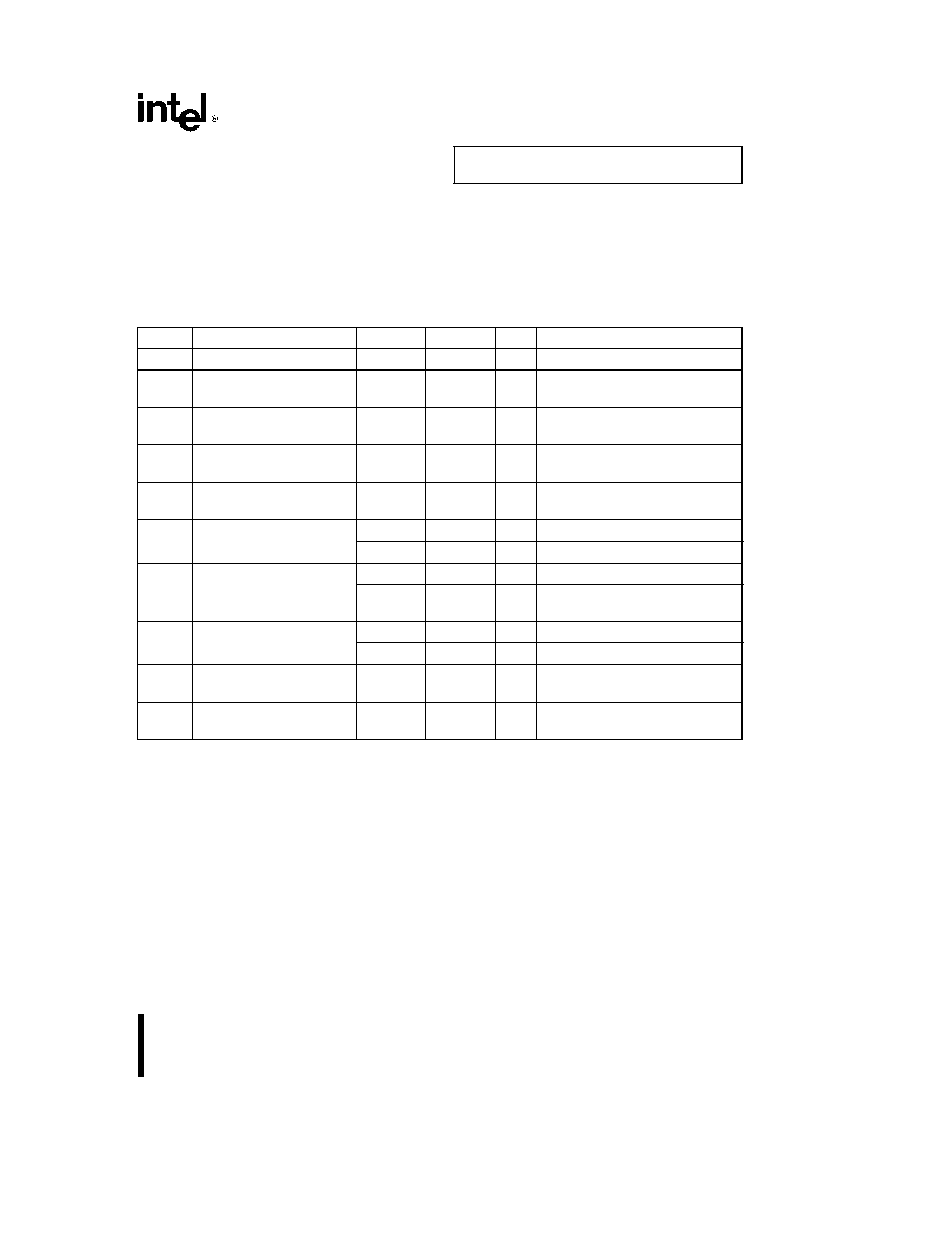
UPI-452
ABSOLUTE MAXIMUM RATINGS
Ambient Temperature Under Bias
0 C to 70 C
Storage Temperature
b
65 C to a150 C
Voltage on Any
Pin to V
SS
b
0 5V to V
CC
a
0 5V
Voltage on V
CC
to V
SS
b
0 5V to a6 5V
Power Dissipation
1 0W
NOTICE This is a production data sheet The specifi-
cations are subject to change without notice
WARNING Stressing the device beyond the ``Absolute
Maximum Ratings'' may cause permanent damage
These are stress ratings only Operation beyond the
``Operating Conditions'' is not recommended and ex-
tended exposure beyond the ``Operating Conditions''
may affect device reliability
D C CHARACTERISTICS
T
A
e
0 C to 70 C V
CC
e
5V
g
10% V
SS
e
0V
Symbol
Parameter
Min
Max
Units
Test Conditions
V
IL
Input Low Voltage
b
0 5
0 8
V
V
IH
Input High Voltage
2 0
V
CC
a
0 5
V
(except XTAL1 RST)
V
IH1
Input High Voltage
3 9
V
CC
a
0 5
V
(XTAL1 RST)
V
OL
Output Low Voltage
0 45
V
I
OL
e
1 6 mA (Note 1)
(Ports 1 2 3 4)
V
OL1
Output Low Voltage
0 45
V
I
OL
e
3 2 mA (Note 1)
(except Ports 1 2 3 4)
V
OH
Output High Voltage
2 4
V
I
OH
e b
60 mA V
CC
e
5V
g
10%
(Ports 1 2 3 4)
0 9 V
CC
V
I
OH
e b
10 mA
V
OH1
Output High Voltage
2 4
V
I
OH
e b
400 mA V
CC
e
5V
g
10%
(except Ports 1 2 3 4 and
0 9 V
CC
V
I
OH
e b
40 mA (Note 2)
Host Interface (Slave) Port)
V
OH2
Output High Voltage
2 4
V
I
OH
e b
400 mA V
CC
e
5V
g
10%
(Host Interface (Slave) Port)
V
CC
b
0 4
V
I
OH
e b
10 mA
I
IL
Logical 0 Input Current
b
50
m
A
V
IN
e
0 45V
(Ports 1 2 3 4)
I
TL
Logical 1 to 0 Transition
b
650
m
A
V
IN
e
2V
Current (Ports 1 2 3 4)
45
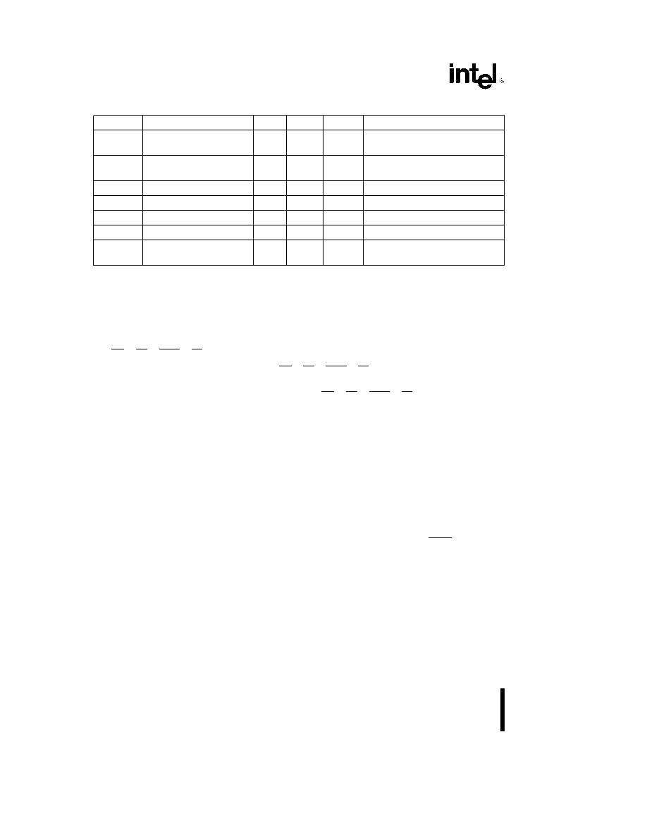
UPI-452
D C CHARACTERISTICS
T
A
e
0 C to 70 C V
CC
e
5V
g
10% V
SS
e
0V (Continued)
Symbol
Parameter
Min
Max
Units
Test Conditions
I
LI
Input Leakage Current
g
10
m
A
0 45V
k
V
IN
k
V
CC
(except Ports 1 2 3 4)
I
OZ
Output Leakage Current
g
10
m
A
0 45V
k
V
OUT
k
V
CC
(except Ports 1 2 3 4)
I
CC
Operating Current
50
mA
V
CC
e
5 5V 14 MHz (Note 4)
I
CCI
Idle Mode Current
25
mA
V
CC
e
5 5V 14 MHz (Note 5)
I
PD
Power Down Current
100
m
A
V
CC
e
2V (Note 3)
RRST
Reset Pulldown Resistor
50
150
KX
CIO
Pin Capacitance
20
pF
1 MHz T
A
e
25 C
(sampled not tested on all parts)
NOTES
1 Capacitive loading on Ports 0 and 2 may cause spurious noise pulses to be superimposed on the V
OLS
of ALE and Ports
1 and 3 The noise is due to external bus capacitance discharging into the Port 0 and Port 2 pins when these pins make 1-
to-0 transitions during bus operations In the worst cases (capacitive loading
l
100 pF) the noise pulse on the ALE line may
exceed 0 8V In such cases it may be desirable to qualify ALE with a Schmitt Trigger or use an address latch with a Schmitt
Trigger STROBE input
2 Capacitive loading on Ports 0 and 2 may cause the V
OH
on ALE and PSEN to momentarily fall before the 0 9 V
CC
specification when the address bits are stabilizing
3 Power DOWN I
CC
is measured with all output pins disconnected EA
e
Port 0
e
V
CC
XTAL2 N C RST
e
V
SS
DB
e
V
CC
WR
e
RD
e
DACK
e
CS
e
A0
e
A1
e
A2
e
V
CC
Power Down Mode is not supported on the 87C452P
4 I
CC
is measured with all output pins disconnected XTAL1 driven with TCLCH TCHCL
e
5 ns V
IL
e
V
SS
a
0 5V V
IH
e
V
CC
b
0 5V XTAL2 N C EA
e
RST
e
Port 0
e
V
CC
WR
e
RD
e
DACK
e
CS
e
A0
e
A1
e
A2
e
V
CC
I
CC
would be
slightly higher if a crystal oscillator is used
5 Idle I
CC
is measured with all output pins disconnected XTAL1 driven with TCLCH TCHCL
e
5 ns V
IL
e
V
SS
a
0 5V
V
IH
e
V
CC
b
0 5V XTAL2 N C Port 0
e
V
CC
EA
e
RST
e
V
SS
WR
e
RD
e
DACK
e
CS
e
A0
e
A1
e
A2
e
V
CC
EXPLANATION OF THE AC SYMBOLS
Each timing symbol has 5 characters The first char-
acter is always a `T' (stands for time) The other
characters depending on their positions stand for
the name of a signal or the logical status of that
signal The following is a list of all the characters and
what they stand for
A Address
C Clock
D Input data
H Logic level HIGH
I
Instruction (program memory contents)
L
Logic level LOW or ALE
P PSEN
Q Output data
R READ signal
T Time
V Valid
W WRITE signal
X No longer a valid logic level
Z Float
EXAMPLE
TAVLL e Time for Address Valid to ALE Low
TLLPL e Time for ALE Low to PSEN Low
46
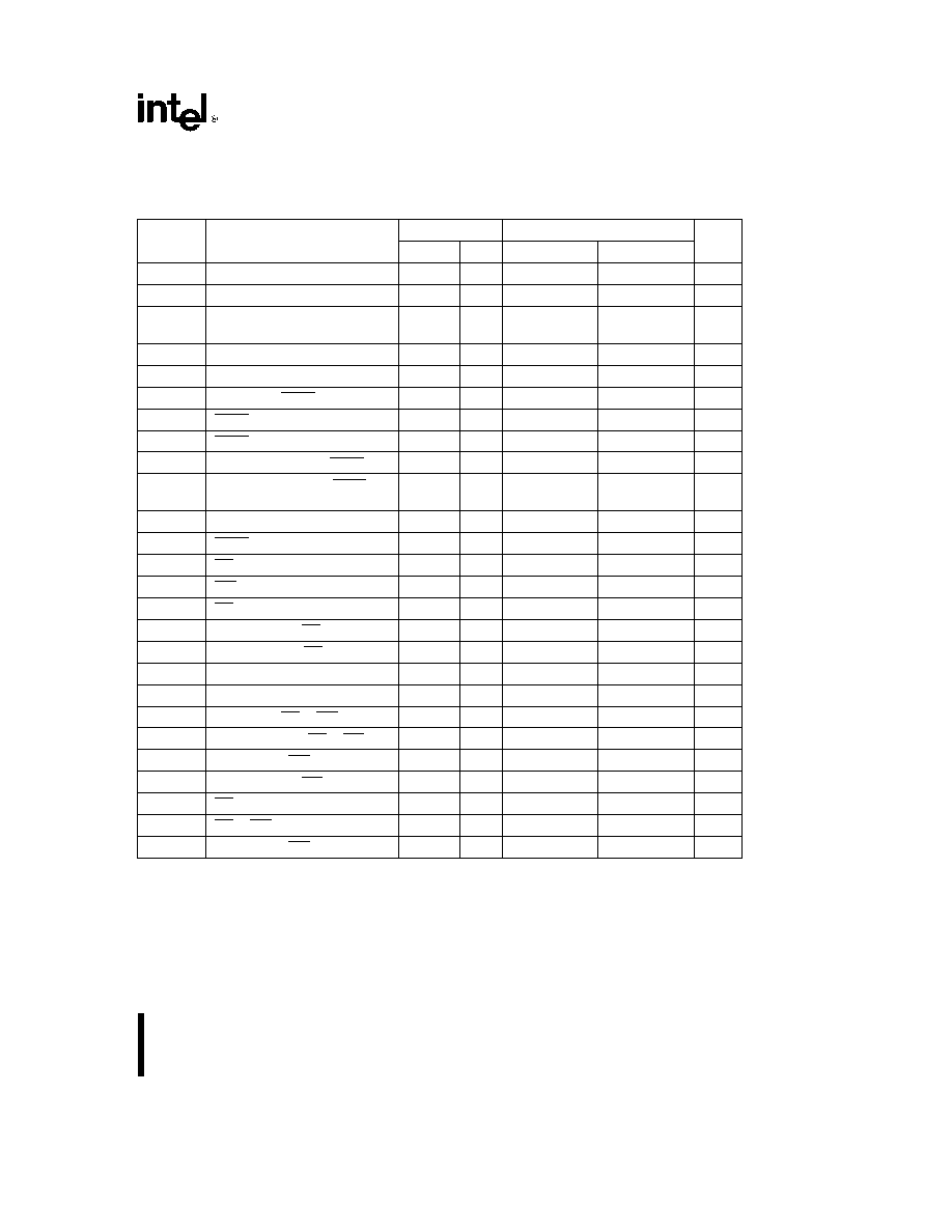
UPI-452
A C CHARACTERISTICS
T
A
e
0 C to 70 C V
CC
e
5V
g
10% V
SS
e
0V Load Capacitance for
Port 0 ALE and PSEN e 100 pF Load Capacitance for All Other Outputs e 80 pF
EXTERNAL PROGRAM AND DATA MEMORY CHARACTERISTICS
Symbol
Parameter
14 MHz Osc
Variable Oscillator
Units
Min
Max
Min
Max
1 TCLCL
Oscillator Frequency
3 5
14
MHz
TLHLL
ALE Pulse Width
103
2TCLCLb40
ns
TAVLL
Address Valid to ALE Low
25
TCLCLb55
ns
(Note 1)
TLLAX
Address Hold after ALE Low
36
TCLCLb35
ns
TLLIV
ALE Low to Valid Instr In
185
4TCLCLb100
ns
TLLPL
ALE Low to PSEN Low
31
TCLCLb40
ns
TPLPH
PSEN Pulse Width
169
3TCLCLb45
ns
TPLIV
PSEN Low to Valid Instr In
110
3TCLCLb105
ns
TPXIX
Input Instr Hold after PSEN
0
0
ns
TPXIZ
Input Instr Float after PSEN
57
TCLCLb25
ns
(Note 1)
TAVIV
Address to Valid Instr In
252
5TCLCLb105
ns
TPLAZ
PSEN Low to Address Float
10
10
ns
TRLRH
RD Pulse Width
329
6TCLCLb100
ns
TWLWH
WR Pulse Width
329
6TCLCLb100
ns
TRLDV
RD Low to Valid Data In
192
5TCLCLb165
ns
TRHDX
Data Hold after RD
0
0
ns
TRHDZ
Data Float after RD
73
2TCLCLb70
ns
TLLDV
ALE Low to Valid Data In
422
8TCLCLb150
ns
TAVDV
Address to Valid Data In
478
9TCLCLb165
ns
TLLWL
ALE Low to RD or WR Low
164
264
3TCLCLb50
3TCLCLa50
ns
TAVWL
Address Valid to RD or WR Low
156
4TCLCLb130
ns
TQVWX
Data Valid to WR Transition
11
TCLCLb60
ns
TWHQX
Data Hold after WR
21
TCLCLb50
ns
TRLAZ
RD Low to Address Float
0
0
ns
TWHLH
RD or WR High to ALE High
31
111
TCLCLb40
TCLCLa40
ns
TQVWH
Data Valid to WR (Setup Time)
350
7TCLCLb150
ns
NOTE
1 Use the value of 14 MHz specification or variable oscillator specification whichever is greater
47
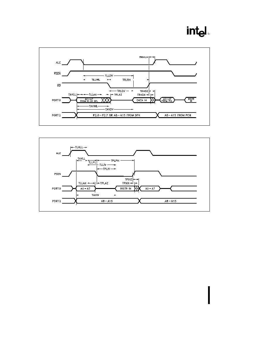
UPI-452
EXTERNAL DATA MEMORY READ CYCLE
231428 � 19
EXTERNAL PROGRAM MEMORY READ CYCLE
231428 � 20
48
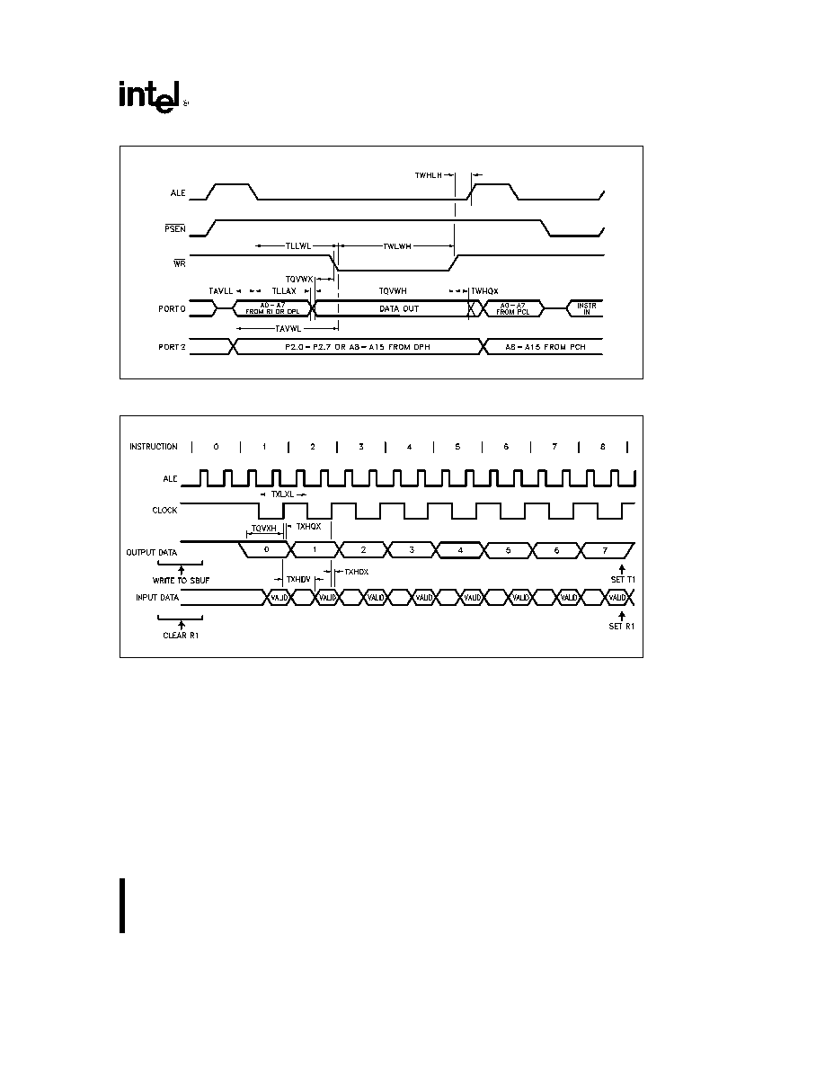
UPI-452
EXTERNAL DATA MEMORY WRITE CYCLE
231428 � 21
SHIFT REGISTER MODE TIMING WAVEFORMS
231428 � 22
49
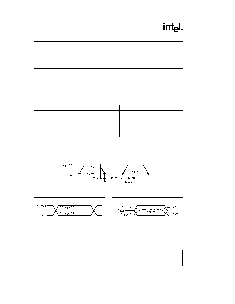
UPI-452
EXTERNAL CLOCK DRIVE
Symbol
Parameter
Min
Max
Units
1 TCLCL
Oscillator Frequency
3 5
14
MHz
TCHCX
High Time
20
ns
TCLCX
Low Time
20
ns
TCLCH
Rise Time
20
ns
TCHCL
Fall Time
20
ns
NOTE
External clock timings are sampled not tested on all parts
SERIAL PORT TIMING
SHIFT REGISTER MODE
Test Conditions T
A
e
0 C to 70 C V
CC
e
5V
g
10% V
SS
e
0V Load Capacitance e 80 pF
Symbol
Parameter
14 MHz Osc
Variable Oscillator
Units
Min
Max
Min
Max
TXLXL
(1)
Serial Port Clock Cycle Time
857
12TCLCL
ns
TQVXH
Output Data Setup to Clock Rising Edge
581
10TCLCLb133
ns
TXHQX
Output Data Hold after Clock Rising Edge
26
2TCLCLb117
ns
TXHDX
Input Data Hold after Clock Rising Edge
0
0
ns
TXHDV
Clock Rising Edge to Input Data Valid
581
10TCLCLb133
ns
NOTE
1 The tolerance of this signal is a function of the input oscillator frequency (TXLXL
e
12TCLCL)
EXTERNAL CLOCK DRIVE WAVEFORM
231428 � 23
AC TESTING INPUT OUTPUT WAVEFORMS
231428 � 24
AC inputs during testing are driven at V
CC
b
0 5V for a logic ``1''
and 0 45V for a logic ``0'' Timing measurements are made at V
IH
min for a logic ``1'' and V
IL
max for a logic ``0''
FLOAT WAVEFORMS
231428 � 25
For timing purposes a port pin is no longer floating when a
100 mV change from load voltage occurs and begins to float
when a 100 mV change from the loaded V
OH
V
OL
level occurs
I
OL
I
OH
t
g
20 mA
50
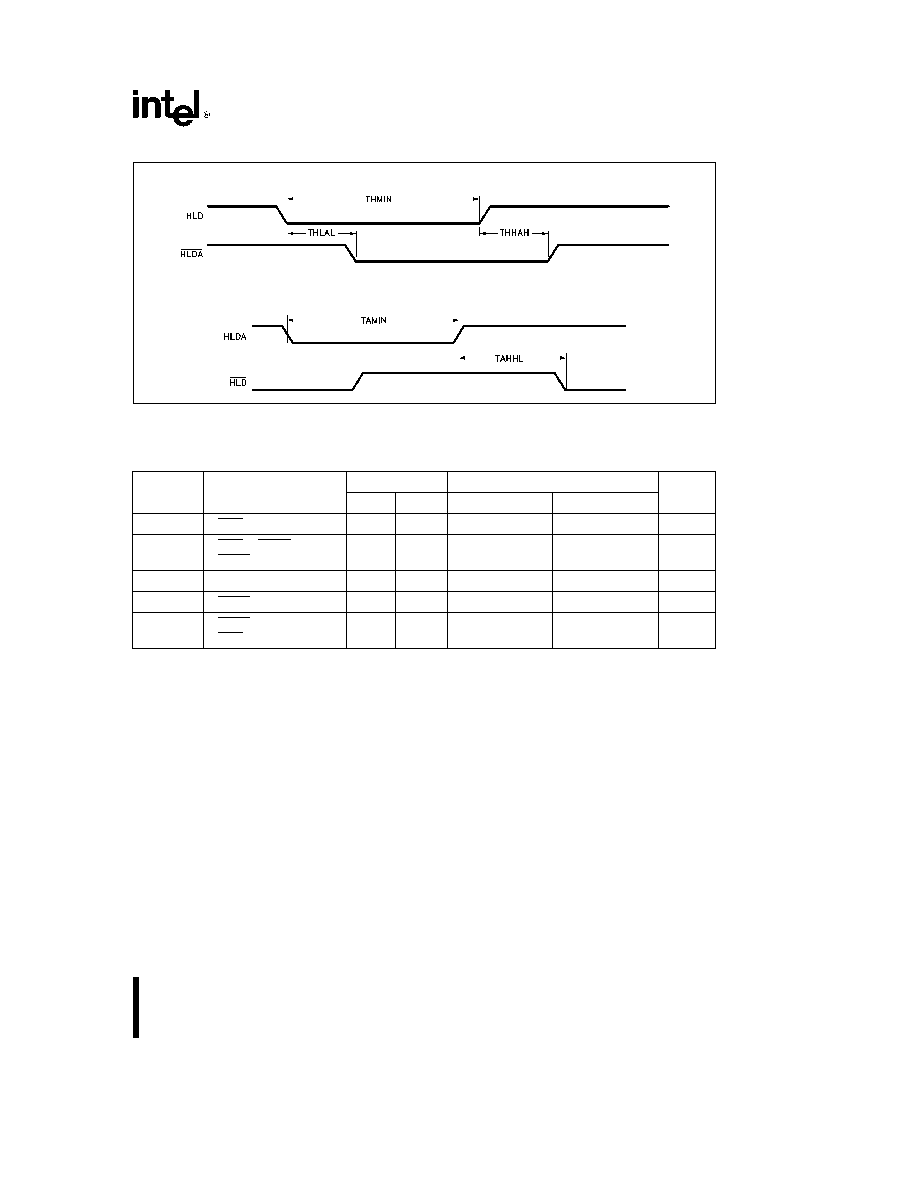
UPI-452
HLD HLDA WAVEFORMS
Arbiter Mode
231428 � 26
Requestor Mode
231428 � 31
HLD HLDA TIMINGS
Test Conditions T
A
e
0 C to a70 C V
CC
e
5V
g
10% V
SS
e
0V Load Capacitance e 80 pF
Symbol
Parameter
14 MHz Osc
Variable Oscillator
Units
Min
Max
Min
Max
THMIN
HLD Pulse Width
386
4TCLCLa100
ns
THLAL
HLD to HLDA Delay if
186
672
4TCLCLb100
8TCLCLa100
ns
HLDA is Granted
THHAH
HLD to HLDA Delay
186
672
4TCLCLb100
8TCLCLa100
ns
TAMIN
HLDA Pulse Width
386
4TCLCLa100
ns
TAHHL
HLDA Inactive to
186
4TCLCLb100
ns
HLD Active
51

UPI-452
HOST PORT WAVEFORMS
231428 � 27
HOST PORT TIMINGS
Test Conditions T
A
e
0 C to 70 C V
CC
e
5V
g
10% V
SS
e
0V Load Capacitance e 80 pF
Symbol
Parameter
14 MHz Osc
Variable Oscillator
Units
Min
Max
Min
Max
TCC
Cycle Time
429
6TCLCL
ns
TPW
Command Pulse Width
100
100
ns
TRV
Recovery Time
60
60
ns
TAS
Address Setup Time
5
5
ns
TAH
Address Hold Time
30
30
ns
TDS
WRITE Data Setup Time
30
30
ns
TDHW
WRITE Data Hold Time
5
5
ns
TDHR
READ Data Hold Time
7
40
7
40
ns
TDV
READ Active to Read
92
92
ns
Data Valid Delay
TDR
WRITE Inactive to Read
343
4 8TCLCL
ns
Data Valid Delay
(Applies only to Host
Control SFR)
TRQ
READ or WRITE Active
150
150
ns
to DRQIN or DRQOUT
Inactive Delay
52

UPI-452
REVISION HISTORY
DOCUMENT
UPI-452 Data Sheet
OLD REVISION NUMBER
231428-005
NEW REVISION NUMBER
231428-006
1 Maximum Clock Rate was changed from 16 MHz to 14 MHz This change is reflected in all Maximum Timing
specifications
2 The proper range of values for ITHR has been changed from 0 to (CBP-2)
to
0 to (CBP-3)
to ensure
proper setting of the Input FIFO request for service bit See the following sections INPUT FIFO CHANNEL
and INPUT AND OUTPUT FIFO THRESHOLD SFR (ITHR
OTHR)
3 The proper range of values for OTHR has been changed from 1 to (80H-CBP)-1
to 2 to (80-CBP)-1
to ensure proper setting of the Output FIFO request for service bit See the following sections OUTPUT
FIFO CHANNEL FIFO-EXTERNAL HOST INTERFACE FIFO DMA FREEZE MODE and INPUT AND OUT-
PUT FIFO THRESHOLD SFR (ITHR
OTHR)
4 The following D C Characteristics were deleted from the data sheet
V
OH
e
0 75 V
CC
I
OH
e b
25 mA
V
OH1
e
0 75 V
CC
I
OH
e
150 mA
V
OH2
e
3 0V
I
OH
e
1 mA and
I
CC1
e
15 mA
V
CC
e
5 5V (87C452P)
See D C CHARACTERISTICS TABLE
5 The parameter descriptions for THHAH and THLAL has been reversed and their maximum specification for
clock rates less than 14 MHz has been changed from 4TCLC a 100 ns to 8TCLC a 100 ns
See
HLD HLDA TIMINGS
6 TAMIN specification has been removed from the Arbiter Mode waveform diagram and added to the Request-
or Mode waveform diagram See HLD HLDA WAVEFORMS
7 Minimum TDHR timing changed from 5 ns to 7 ns
53