01/99
B-5
2N3954, 2N3955, 2N3956
N-Channel Dual Silicon Junction Field-Effect Transistor
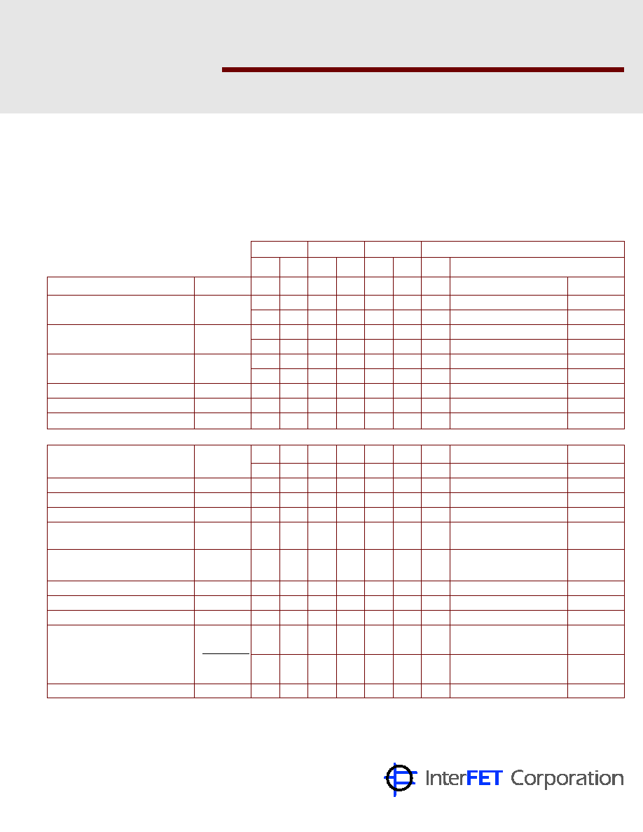
Absolute maximum ratings at T
A
= 25°C
Reverse Gate Source & Reverse Gate Drain Voltage
≠ 50 V
Gate Current
50 mA
Total Device Power Dissipation (each side)
250 mW
@ 85∞C Case Temperature (both sides)
500 mW
Power Derating (both sides)
4.3 mW/∞C
TO–71 Package
See Section G for Outline Dimensions
Pin Configuration
1 Source, 2 Drain, 3 Gate,
5 Source, 6 Drain, 7 Gate
At 25∞C free air temperature:
2N3954
2N3955
2N3956
Process NJ16
Static Electrical Characteristics
Min
Max
Min
Max
Min
Max
Unit
Test Conditions
Gate Source Breakdown Voltage
V
(BR)GSS
≠ 50
≠ 50
≠ 50
V
I
G
= ≠ 1µA, V
DS
= ÿV
Gate Reverse Current
I
GSS
≠ 100
≠ 100
≠ 100
pA
V
GS
= ≠ 30V, V
DS
= ÿV
≠ 500
≠ 500
≠ 500
nA
V
GS
= ≠ 30V, V
DS
= ÿV
T
A
= 125∞C
Gate Operating Current
I
G
≠ 50
≠ 50
≠ 50
pA
V
DS
= 20V, I
D
= 200 µA
≠ 250
≠ 250
≠ 250
nA
V
DS
= 20V, I
D
= 200 µA
T
A
= 125∞C
Gate Source Voltage
V
GS
≠ 4.2
≠ 4.2
≠ 4.2
V
V
DS
= 20V, I
D
= 50 µA
≠ 0.5
≠ 4
≠ 0.5
≠ 4
≠ 0.5
≠ 4
V
V
DS
= 20V, I
D
= 200 µA
Gate Source Cutoff Voltage
V
GS(OFF)
≠ 1
≠ 4.5
≠ 1
≠ 4.5
≠ 1
≠ 4.5
V
V
DS
= ≠ 20V, I
G
= 1 nA
Gate Source Forward Voltage
V
GS(F)
2
2
2
V
V
DS
= ÿV, I
G
= 1 mA
Drain Saturation Current (Pulsed)
I
DSS
0.5
5
0.5
5
0.5
5
mA
V
DS
= 20V, V
GS
= ÿV
Dynamic Electrical Characteristics
Common Source Forward
g
fs
1000
3000
1000
3000
1000
3000
µS
V
DS
= 20V, V
GS
= ÿV
f = 1 kHz
Transconductance
1000
1000
1000
µS
V
DS
= 20V, V
GS
= ÿV
f = 200 MHz
Common Source Output Capacitance
g
os
35
35
35
µS
V
DS
= 20V, V
GS
= ÿV
f = 1 kHz
Common Source Input Capacitance
C
iss
4
4
4
pF
V
DS
= 20V, V
GS
= ÿV
f = 1 MHz
Drain Gate Capacitance
C
dgo
1.5
1.5
1.5
pF
V
dg
= 10V, I
S
= ÿA
f = 1 MHz
Common Source Reverse
C
rss
1.2
1.2
1.2
pF
V
DS
= 20V, V
GS
= ÿV
f = 1 MHz
Transfer Capacitance
Noise Figure
NF
0.5
0.5
0.5
dB
V
DS
= 20V, V
GS
= ÿV,
f = 100 Hz
R
g
= 10 M
Differential Gate Current
| I
G1
≠ I
G2
|
10
10
10
nA
V
DS
= 20V, I
D
= 200µA
T
A
= 125∞C
Saturation Drain Current Ratio
I
DSS1
/I
DSS2
0.95
1
0.95
1
0.95
1
V
DS
= 20V, V
GS
= ÿV
Differential Gate Source Voltage
| V
GS1
≠ V
GS2
|
5
10
15
mV
V
DS
= 20V, I
D
= 200µA
T
A
= 25∞C
Differential Gate Source Voltage
V
GS1
≠ V
GS2
0.8
2
4
mV/∞C
V
DS
= 20V, I
D
= 200µA
to = ≠ 55∞C
with Temperature
T
T
A
= 25∞C
1
2.5
5
mV/∞C
V
DS
= 20V, I
D
= 200µA
to = +125∞C
Transconductance Ratio
g
fs1
/g
fs2
0.97
1
0.97
1
0.97
1
V
DS
= 20V, I
D
= 200µA
f = 1 kHz
• Low and Medium Frequency
Differential Amplifiers
• High Input Impedance
Amplifiers
1000 N. Shiloh Road, Garland, TX 75042
(972) 487-1287
FAX
(972) 276-3375
www.interfet.com
Databook.fxp 1/14/99 11:29 AM Page B-5