D-4
01/99
IFN112
N-Channel Silicon Junction Field-Effect Transistor
• Low-Noise, High Gain
• Equivalent to Japanese 2SK112
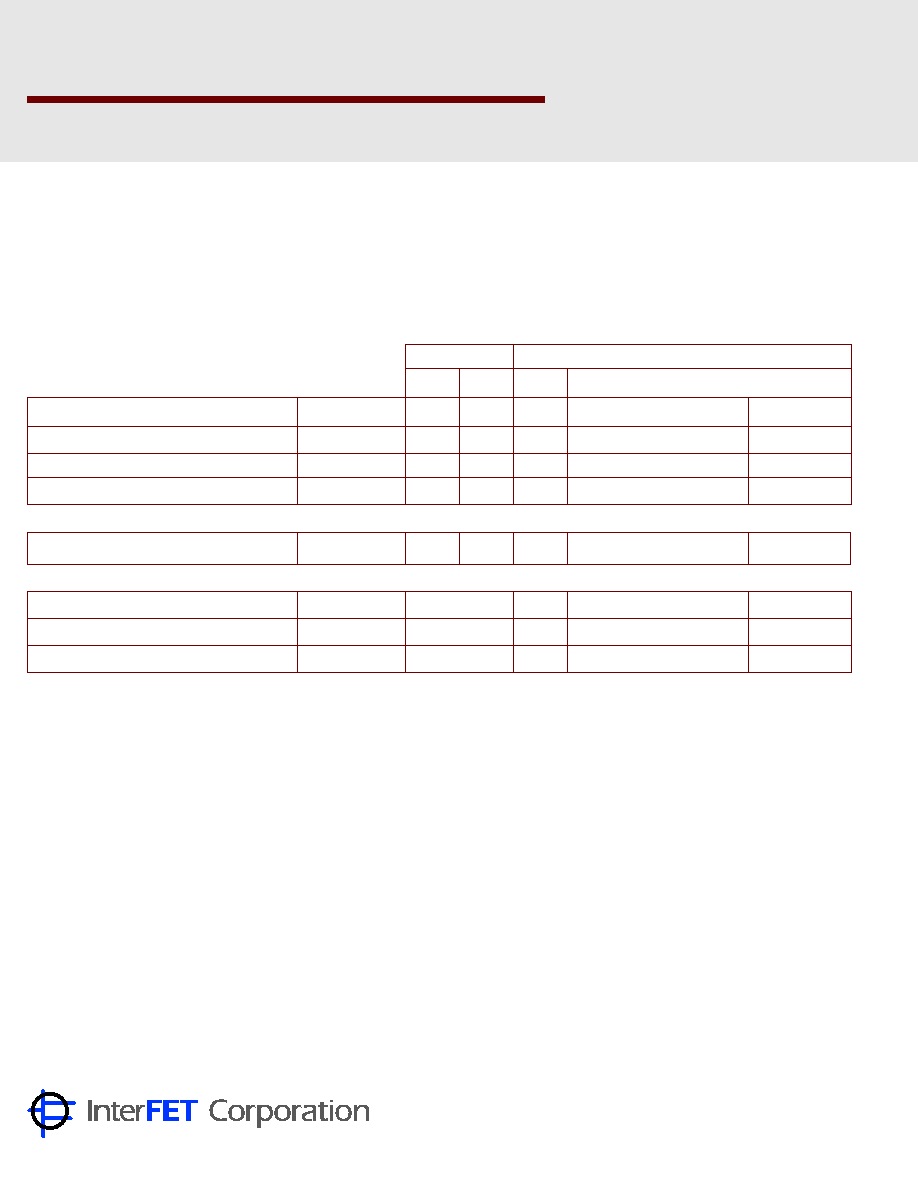
Absolute maximum ratings at T
A
= 25°C
Reverse Gate Source & Reverse Gate Drain Voltage
≠ 50 V
Continuous Forward Gate Current
10 mA
Continuous Device Power Dissipation
360 mW
Power Derating
2.88 mW/įC
Storage Temperature Range
≠ 65įC to 200įC
TO–18 Package
Dimensions in Inches (mm)
Pin Configuration
1 Source, 2 Drain, 3 Gate & Case
At 25įC free air temperature:
IFN112
Process NJ132H
Static Electrical Characteristics
Min
Max
Unit
Test Conditions
Gate Source Breakdown Voltage
V
(BR)GSS
≠ 50
V
I
G
= ≠ 1 ĶA, V
DS
= ōV
Gate Reverse Current
I
GSS
≠ 0.1
nA
V
DS
= ōV, V
GS
= ≠ 30V
Gate Source Cutoff Voltage
V
GS(OFF)
≠ 0.25
≠ 1.2
V
V
DS
= 15V, I
D
= 100 nA
Drain Saturation Current (Pulsed)
I
DSS
1.2
9.0
mA
V
DS
= 15V, V
GS
= ōV
Dynamic Electrical Characteristics
Common Source Forward Transconductance
g
fs
7
34
mS
V
DS
= 15V, V
GS
= ōV
f = 1 kHz
Typ
Common Source Input Capacitance
C
iss
12
pF
V
DS
= 15V, V
GS
= ōV
f = 1 MHz
Common Source Reverse Transfer Capacitance
C
rss
3
pF
V
DS
= 15V, V
GS
= ōV
f = 1 MHz
Equivalent Short Circuit Input Noise Voltage
Įe
N
2.5
nV/
Hz
V
DS
= 10V, I
D
= 5.0 mA
f = 1 kHz
1000 N. Shiloh Road, Garland, TX 75042
(972) 487-1287
FAX
(972) 276-3375
www.interfet.com
Databook.fxp 1/13/99 2:09 PM Page D-4