 | –≠–ª–µ–∫—Ç—Ä–æ–Ω–Ω—ã–π –∫–æ–º–ø–æ–Ω–µ–Ω—Ç: MHE1212S | –°–∫–∞—á–∞—Ç—å:  PDF PDF  ZIP ZIP |

MODELS
VDC O
UTPUT
SINGLE
5
12
15
DUAL
±12
±15
DESCRIPTION
The MHE SeriesTM and the MLP SeriesTM DC/DC converters offer
the high efficiencies associated with switching regulators, yet have
full isolation and the excellent regulation typical of linear regulators.
No external components are required for operation. MHE Series and
MLP Series converters are built using thick-film hybrid technology,
and are sealed in metal packages for military, aerospace, and other
high-reliability applications. Unscreened models are solder sealed
and are guaranteed to pass a gross leak test (maximum leak rate of
1 x 10
-3
atm.-cc/sec). Environmentally screened models are
hermetically sealed and are screened as described in Section C2.
The MHE Series and MLP Series converters are pulse-width modu-
lated switching regulators operating in the forward mode, with a
nominal switching frequency of 125 to 140 kHz. Isolation is achieved
through the use of a transformer in the forward power circuit, and an
optocoupler is used in the feedback/control loop. The full load output
power is available over the full input voltage range. Short-term tran-
sients of 50 volts will not impair normal operation for 28 volt input
models.
The efficiency is typically greater than 80% over the entire input
voltage range and from approximately 25% of full load to full load.
This feature makes the MHE/MLP Series converters ideal for either
battery or aircraft power applications.
An inhibit function is provided on MHE/MLP Series converters to
allow power shutdown and startup from a logic input. The unit is
inhibited when the inhibit input pin (pin 2) is connected to the input
common (pin 10). The open circuit voltage of the inhibit pin is 8 to
10 VDC for 12 V input models or 11 to 13 VDC for 28 V input
models. During inhibit, the input inhibit pin must sink approximately
1 mA. In the inhibit mode, converter output drops to less than 1 V
and the input current is typically 8 mA.
Automatic current limiting circuitry protects the MHE/MLP Series
converters against short circuits.
MHE/MLP Series converters are rated to operate at full load up to a
case temperature of 85∞C, with the output power derated linearly to
zero at 115∞C. Because of the unit's high efficiency, heat sinking
requirements are minimized, but due consideration should be given
to removing self-generated heat when operating the device at
maximum ratings. To increase dissipation, heat conducting material
(PCB, copper sheet, heat sink, etc.) should be brought into contact
with the converter's baseplate.
When the MHE/MLP Series converters are used in applications
requiring full power operation for extended periods of time, or in
shock and vibration environments, it is highly recommended that the
flange-mount option be used. This option provides improved thermal
transfer capabilities as well as a mechanically secure mounting
configuration.
DC/DC C
ONVERTERS
12
AND
28 V
OLT
I
NPUT
MHE/MLP SERIES
20 WATT
B4-13
Size (max.): Non-flanged 2.125 x 1.125 x 0.495 MHE (case H6) inches
or 0.417 MLP (case H4)
(53.98 x 28.58 x 12.57 (MHE) or 10.59 (MLP) mm)
Flanged 2.910 x 1.125 x 0.495 MHE (case K7) inches
or 0.417 MLP (case K5)
(73.91 x 28.58 x 12.57 (MHE) or 10.59 (MLP) mm)
See Section B8, cases H4, H6, K5, and K7, for dimensions.
Weight:
50 grams typical
Screening: Standard or ES. See Section C2 for screening options, see
Section A5 for ordering information.
F
EATURES
∑ ≠55∞C to +85∞C operation
∑ 10 to 16 VDC input or
16 to 36 VDC input typical
∑ Fully isolated
∑ Opto-coupler feedback
∑ Fixed frequency 125 kHz typical
∑ Topology ≠ Push-Pull Forward
∑ Transient protection
50 V for up to 50 ms 28 Vin models
∑ Inhibit function
∑ Indefinite short circuit protection
∑ Trimmable output on single models
∑ Up to 83% efficiency

TYPICAL CHARACTERISTICS
ABSOLUTE MAXIMUM RATINGS
RECOMMENDED OPERATING CONDITIONS
INHIBIT
Output Power
∑ 10 to 20 watts depending on model
Lead Soldering Temperature (10 sec per lead)
∑ 300∞C
Storage Temperature Range (Case)
∑ ≠55∞C to +125∞C
B4-14
MHE/MLP SERIES
20 WATT
DC/DC C
ONVERTERS
Output Voltage Temperature Coefficient
∑ 150 ppm/∞C, typical
Input to Output Capacitance
∑ 60 pF, typical
Current Limit
∑ 125% of full load, typical
Isolation
∑ 100 megohm minimum at 500 V
Conversion Frequency
∑ 125 kHz, typical
Inhibit Pin Voltage (unit enabled)
∑ 11 to 13 V MHE28XXX, MLP28XXX
∑ 8 to 10 V MHE12XXX
Input Voltage Range
Continuous
∑ 17 to 40 VDC MHE28XXX
∑ 10 to 16 VDC MHE12XXX
∑ 16 to 40 VDC MLP28XXX
Transient
∑ 50 V for 50 msec on 28 V input models
Case Operating Temperature (Tc)
∑ ≠55∞C to +85∞C full power
Derating Output Power/Current
∑ Linearly from 100% at 85∞C to 0% at 115∞ C
∑ MHE28XXX models derate by 33% at 16 Vin
Inhibit TTL Open Collector
∑ Logic low (output disabled)
Logic low voltage
0.8 V
∑ Referenced to input common
∑ Logic high (output enabled)
Open collector
Electrical Characteristics: 25∞C Tc, 28 VDC Vin, 100% load, unless otherwise specified.
SINGLE OUTPUT MHE12XX MODELS
MHE1205S
MHE1212S
MHE1215S
PARAMETER
CONDITION
MIN
TYP
MAX
MIN
TYP
MAX
MIN
TYP
MAX
UNITS
OUTPUT VOLTAGE
4.95
5.00
5.05
11.88
12.00
12.12
14.85
15.00
15.15
VDC
OUTPUT CURRENT
≠55∞C TO +85∞C
--
--
3
--
--
1.25
--
--
1.0
A
OUTPUT POWER
≠55∞C TO +85∞C
--
--
15
--
--
15
--
--
15
W
OUTPUT RIPPLE
VOLTAGE
0 TO 1 MHz
--
35
70
--
35
70
--
35
70
mV p-p
LINE REGULATION
V
IN
MIN TO MAX
--
2
5
--
3
10
--
3
10
mV
LOAD REGULATION
NO LOAD TO FULL
--
10
20
--
5
15
--
10
20
mV
INPUT VOLTAGE
CONTINUOUS
10
12
16
10
12
16
10
12
16
VDC
TRANSIENT 50 ms
--
--
--
--
--
--
--
--
--
V
INPUT CURRENT
NO LOAD
--
--
24
--
--
32
--
--
32
mA
INPUT RIPPLE
CURRENT
10 kHz ≠ 2 MHz
--
30
80
--
30
80
--
30
80
mA p-p
EFFICIENCY
78
81
--
79
82
--
80
83
--
%
SINGLE AND DUAL MLP MODELS
MLP2805S
MLP2812S
MLP2815S
MLP2812D
MLP2815D
PARAMETER
CONDITIONS
MIN TYP MAX
MIN TYP MAX
MIN
TYP MAX
MIN
TYP
MAX
MIN
TYP
MAX
UNITS
OUTPUT VOLTAGE
4.95 5.00 5.05
11.88 12.00 12.12 14.85 15.00 15.15
±11.88 ±12.00 ±12.12 ±14.85 ±15.00 ±15.15
VDC
OUTPUT CURRENT
1
≠55 TO +85∞C
--
--
2
--
--
1.25
--
--
1
--
--
±0.41
--
--
±0.33
A
OUTPUT POWER
1
≠55 TO +85∞C
--
--
10
--
--
15
--
--
15
--
--
10
--
--
10
W
OUTPUT RIPPLE
VOLTAGE
0 - 1 MHz
--
25
60
--
30
50
--
30
50
--
30
60
--
30
60
mV p-p
LINE REGULATION
V
IN
MIN TO MAX
--
2
5
--
3
10
--
3
10
--
3
10
--
3
10
mV
LOAD REGULATION
NO LOAD TO FULL
--
10
20
--
5
15
--
5
15
--
5
15
--
5
15
mV
INPUT VOLTAGE
CONTINUOUS
16
28
40
16
28
40
16
28
40
16
28
40
16
28
40
VDC
TRANSIENT 50 ms
--
--
50
--
--
50
--
--
50
--
--
50
--
--
50
V
INPUT CURRENT
NO LOAD
--
--
20
--
--
30
--
--
30
--
--
30
--
--
30
mA
INPUT RIPPLE
CURRENT
10 kHz - 2 MHz
--
20
50
--
25
50
--
25
50
--
25
50
--
25
50
mA p-p
EFFICIENCY
78
81
--
79
82
--
80
83
--
78
81
--
78
81
--
%
B4-15
MHE/MLP SERIES
20 WATT
DC/DC C
ONVERTERS
Note
1. On dual output models at least 25% of the load should be on the positive output.
Electrical Characteristics: 25∞C Tc, 28 VDC Vin (12 Vin for 12 V models), 100% load, unless otherwise specified.
SINGLE AND DUAL MHE28XX MODELS
MHE2805S
MHE2812S
MHE2815S
MHE2812D
MHE2815D
PARAMETER
CONDITIONS
MIN TYP MAX
MIN TYP MAX
MIN
TYP MAX
MIN
TYP
MAX
MIN
TYP
MAX
UNITS
OUTPUT VOLTAGE
4.95 5.00 5.05
11.88 12.00 12.12 14.85 15.00 15.15
±11.88 ±12.00 ±12.12 ±14.85 ±15.00 ±15.15
VDC
OUTPUT CURRENT
1
≠55 TO +85∞C
--
--
3.0
--
--
1.67
--
--
1.33
--
--
±0.63
--
--
±0.5
A
OUTPUT POWER
1
≠55 TO +85∞C
--
--
15
--
--
20
--
--
20
--
--
15
--
--
15
W
OUTPUT RIPPLE
VOLTAGE
0 - 1 MHz
--
35
60
--
60
80
--
30
60
--
30
50
--
30
50
mV p-p
LINE REGULATION
V
IN
MIN TO MAX -- 2 5 -- 3 10 -- 3 10 -- 3 10 -- 3 1
5
mV
LOAD REGULATION
NO LOAD TO FULL
--
10
20
--
5
15
--
5
15
--
5
15
--
5
15
mV
INPUT VOLTAGE
CONTINUOUS
17
28
40
17
28
40
17
28
40
17
28
40
17
28
40
VDC
TRANSIENT 50 ms
--
--
50
--
--
50
--
--
50
--
--
50
--
--
50
V
INPUT CURRENT
NO LOAD
--
--
18
--
--
30
--
--
30
--
--
35
--
--
35
mA
INPUT RIPPLE
CURRENT
10 kHz - 2 MHz
--
20
50
--
25
50
--
25
50
--
25
50
--
25
50
mA p-p
EFFICIENCY
78
81
--
79
82
--
80
83
--
76
79
--
76
79
--
%
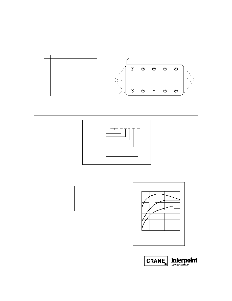
TYPICAL PERFORMANCE CURVE
OUTPUT ADJUSTMENT RESISTOR VALUES
FOR MHE2805S AND MLP2805S
B4-16
MHE/MLP SERIES
20 WATT
DC/DC C
ONVERTERS
F
IGURE
2
Output Power (Watts)
MLP2815S Efficiency
E
ffic
ie
n
c
y
(%
)
72
84
82
80
76
74
2.5
15.0
5.0
7.5
10.0
12.5
78
86
18 V
28 V
36 V
MODEL NUMBERING KEY
MHE 28 12 S F / ES
Base Model
Input Voltage
Output Voltage
Screening
Number of Outputs
Case Option
(Non-flanged case has no designator in
this position)
(S = single, D = dual)
(Standard screening has no designator
in this position.)
PIN OUT
Pin
Single Output
Dual Output
1
Positive Input
Positive Input
2
Inhibit
Inhibit
3
Output Adjust
Positive Output
4
Output Common
Output Common
5
Positive Output
Negative Output
6
No connection
No connection
7
No connection
No connection
8
Case Ground
Case Ground
9
No connection
No connection
10
Input Common
Input Common
BOTTOM VIEW
MHE and MLP
Squared corner and dot on
top of cover indicate pin one.
Dotted line outlines flanged package option.
1
2
6
10
3
4
5
7
8
9
See Section B8, case H4, H6, K5 and K7 for dimensions.
Output Adjustment all single output models:
The output can be adjusted upward by using the output
adjust (pin3). The resistance between output adjust (pin 3)
and output common (pin 4) will determine the magnitude of
the increase in the output. The table above is applicable
only to MHE2805S and MLP2805S.
Resistance
Output Voltage
Pin 3 to 4
Increase (%)
0
390K
+1%
145K
+2%
63K
+3%
22K
+4%
0
+5%
F
IGURE
1: P
IN
O
UT
22820-001-DTS Rev
B
All technical information is believed to be accurate, but no responsibility is assumed for
errors or omissions. Interpoint reserves the right to make changes in products or spec-
ifications without notice. MHE Series and MLP Series are trademarks of Interpoint.
Copyright © 1995 - 1999 Interpoint. All rights reserved.

B8-17
CASE H
C
ASES
CASE H
BOTTOM VIEW
See Figures 29 ≠ 34
for pin configurations.
2.125 max
(53.98)
1.125 max
(28.58)
Materials
Header Cold Rolled Steel/Nickel/Gold
cases H1 and H2
Cold Rolled Steel/Nickel/Tin
cases H3, H4, and H5
Cover Kovar/Nickel
cases H1 and H2
Cold Rolled Steel/Nickel/Tin
cases H3, H4, and H5
Pins #52
alloy
ceramic seal
case H1
case H2 (except MHV Series Single and Dual)
compression glass seal
MHV Series Single and Dual
case H3, H4, H5
Case dimensions in inches (mm)
Tolerance
±
0.005 (0.13) for three decimal places
±
0.01 (0.3) for two decimal places
unless otherwise specified
CAUTION
Heat from reflow or wave soldering may damage
the device. Solder pins individually with heat
application not exceeding 300
∞
C for 10 seconds
per pin.
Dot on top of case indicates pin one
0.155 (3.94)
0.955 (24.26)
Seam Seal
0.000
0.040 dia
(1.02)
0.000
0.000
0.400 max.
(10.16)
0.25
±
0.03
(6.4
±
0.8)
0.555 (14.1)
0.245
(6.22)
1.845
(46.86)
2.090
(53.01)
1.110 (28.19)
1
2
3
4
5
FMC EMI Filter: Screening ≠ Standard, ES, or 883
SFMC EMI Filter: Screening ≠ Space Standard, H, or K
BOTTOM VIEW CASE H1
Squared corner and dot on top
of case indicate pin one.
F
IGURE
29: C
ASE
H1
F
IGURE
28: C
ASE
H M
AXIMUM
D
IMENSIONS
Note: Although every effort has been made to render the case drawings at actual size, variations in the printing process may cause some distortion. Please refer
to the numerical dimensions for accuracy.