
1
Size (max.): Non flanged 1.460 x 1.130 x 0.330 (37.08 x 28.70 x 8.38 mm)
Flanged 2.005 x 1.130 x 0.330 (50.93 x 28.70 x 8.38 mm)
Weight:
30 grams maximum.
Screening: Standard, ES, or 883 (Class H).
DESCRIPTION
The MHF+ SeriesTM of high frequency DC/DC converters offers a
wide input voltage range of 16 to 40 volts and up to 15 watts of
output power. The units are capable of withstanding short term tran-
sients up to 50 volts. The package is a hermetically sealed, welded
metal case. Flanged and non-flanged models are available.
C
ONVERTER
D
ESIGN
The MHF+ converters are switching regulators that use a quasi-
square wave, single-ended forward converter design with a constant
switching frequency of 550 kHz. Isolation between input and output
circuits is provided with a transformer in the forward path and a
temperature compensated optical link in the feedback control loop.
For the MHF+ dual output models, good cross regulation is main-
tained by tightly coupled output magnetics. Up to 90% of the total
output power (80% on 2805D) is available from either output,
providing the opposite output is simultaneously carrying 10% of the
total output power (20% on 2805D models). Predictable current limit
is accomplished by directly monitoring the output load current and
providing a constant current output above the overload point.
H
IGHER
P
OWER
D
ENSITY
The MHF+ Series offers a new standard of performance for small
size and high power density. At just 0.33 inch high and a total foot-
print of 1.7 in
2,
this low profile package offers a total power density
of up to 28 watts per cubic inch.
L
OW
N
OISE
, H
IGH
A
UDIO
R
EJECTION
The MHF+ converters' feed-forward compensation system provides
excellent dynamic response and noise rejection. Audio rejection is
typically 50 dB. Typical output voltage response for a 50% to 100%
step load transient is as low as 1.3% with a 150 msec recovery time.
Input ripple current is typically 35 mA p-p with output ripple voltage
typically 30 mV p-p .
I
NHIBIT
F
UNCTION
MHF+ converters provide an inhibit terminal that can be used to
disable internal switching, resulting in no output and very low quies-
cent input current. The converter is inhibited when a TTL compatible
low (
0.8 ≠ output disabled) is applied to the inhibit pin. The unit is
enabled when the pin, which is internally connected to a pull-up
resistor, is left unconnected or is connected to an open-collector
gate. The open circuit output voltage associated with the inhibit pin
is 8.5 to 12 V. In the inhibit mode, a maximum of 4 mA must be sunk
from the inhibit pin.
S
YNCHRONIZATION
A synchronization feature is included with the MHF+ Series that
allows the user to match the switching frequency of the converter to
the frequency of the system clock. An external synchronization
feature is included that allows the user to adjust the nominally 550
kHz operating frequency to any frequency within the range of 500
kHz to 600 kHz. This is initiated by applying a TTL compatible input
of the desired frequency to pin 5.
S
HORT
C
IRCUIT
P
ROTECTION
MHF+ Series converters provide short circuit protection by
restricting the output current to approximately 115% of the full load
output current. The output current is sensed in the secondary stage
to provide highly predictable and accurate current limiting, and to
eliminate foldback characteristics.
U
NDERVOLTAGE
L
OCKOUT
Undervoltage lockout prevents the units from operating below
approximately 12 VDC input voltage to keep system current levels
smooth, especially during initialization or re-start operations.
DC/DC C
ONVERTERS
28 V
OLT
I
NPUT
MHF+ SERIES
SINGLE & DUAL
15 WATT
F
EATURES
∑ ≠55∞ to +125∞C operation
∑ 16 to 40 VDC input
∑ Fully isolated
∑ Optocoupler feedback
∑ Fixed frequency, 550 kHz typical
∑ Topology ≠ Single Ended Forward
∑ 50 V for up to 50 ms transient protection
∑ Inhibit and sync functions
∑ Indefinite short circuit protection
∑ Undervoltage lockout
∑ Up to 84% efficiency, 28 W/in
3
MODELS
VDC O
UTPUT
SINGLE
3.3
5
5.2
12
15
28
DUAL
±5
±12
±15

RECOMMENDED OPERATING CONDITIONS
TYPICAL CHARACTERISTICS
SYNC AND INHIBIT
ABSOLUTE MAXIMUM RATINGS
Input Voltage
∑ 16 to 40 VDC
Power Dissipation (Pd)
∑ 6 W
Output Power
∑ 12 to 15 watts depending on model
Lead Soldering Temperature (10 sec per lead)
∑ 300∞C
Storage Temperature Range (Case)
∑ ≠65∞C to +150∞C
2
DC/DC C
ONVERTERS
Output Voltage Temperature Coefficient
∑ 100 ppm/∞C typical
∑ 150 ppm/∞C maximum
Input to Output Capacitance
∑ 60 pF typical
Undervoltage Lockout
∑ 12 V input typical
Current Limit
∑ 115% of full load typical
Isolation
∑ 100 megohm minimum at 500 V
Audio Rejection
∑ 50 dB typical
Conversion Frequency (55∞C to +125∞C Tc)
∑ Free run 550 kHz typical
480 kHz min, 620 kHz max
Inhibit Pin Voltage (unit enabled)
∑ 8.5 to 12 V
Input Voltage Range
∑ 16 to 40 VDC continuous
∑ 50 V for up to 50 msec transient
Case Operating Temperature (Tc)
∑ ≠55∞C to +125∞C full power
∑ ≠55∞C to +135∞C absolute
Derating Output Power/Current (Tc)
∑ Linearly from 100% at 125∞C to 0% at 135∞C
MHF+ SERIES
SINGLE AND DUAL
15 WATT
SINGLE OUTPUT MODELS
MHF+283R3S
MHF+2805S
MHF+285R2S
PARAMETER
CONDITION
MIN TYP MAX
MIN
TYP MAX
MIN
TYP MAX
UNITS
OUTPUT VOLTAGE
3.27
3.30
3.33
4.95
5.00
5.05
5.16
5.20
5.24
VDC
OUTPUT CURRENT
V
IN
= 16 to 40 VDC
0
--
2.4
0
--
2.4
0
--
2.4
A
OUTPUT POWER
V
IN
= 16 to 40 VDC
0
--
8
0
--
12
0
--
12.48
W
OUTPUT RIPPLE
10 kHz - 2 MHz
--
30
80
--
30
80
--
30
50
mV p-p
VOLTAGE
Tc = ≠55∞C to +125∞C
--
50
120
--
60
100
--
60
100
LINE REGULATION
Vin = 16 to 40 VDC
--
5
100
--
5
50
--
5
35
mV
LOAD REGULATION
NO LOAD TO FULL
--
20
50
--
20
50
--
20
35
mV
INPUT VOLTAGE
CONTINUOUS
16
28
40
16
28
40
16
28
40
VDC
NO LOAD TO FULL
TRANSIENT 50 ms
--
--
50
--
--
50
--
--
50
V
INPUT CURRENT
NO LOAD
--
25
65
--
25
40
--
25
42
FULL LOAD
--
--
397
--
560
624
--
560
605
mA
INHIBITED
--
5
12
--
5
12
--
5
12
INPUT RIPPLE
10 kHz - 10 MHz
--
45
80
--
35
80
--
35
100
CURRENT
Tc = ≠55∞C to +125∞C
--
--
120
--
--
100
--
--
100
mA pp
EFFICIENCY
72
75
--
75
77
--
75
77
--
%
LOAD FAULT
1
SHORT CIRCUIT
POWER DISSIPATION
--
5
8
--
3.5
6
--
3.5
6
W
RECOVERY
2
--
7.5
30
--
7.5
30
--
7.5
30
ms
STEP LOAD RESP.
50% ≠ 100% ≠ 50%
TRANSIENT
≠400
150
500
≠400
150
400
≠400
150
400
mV pk
RECOVERY
2
--
150
300
--
150
300
--
150
300
µs
STEP LINE RESP.
16 ≠ 40 ≠ 16 VDC
TRANSIENT
3
≠800
550
800
≠800
550
800
≠800
550
800
mV pk
RECOVERY
2
--
0.8
1.2
--
0.8
1.2
--
0.8
1.2
ms
START-UP
DELAY
--
10
25
--
10
25
--
10
25
ms
OVERSHOOT
4
--
200
300
--
100
600
--
100
600
mV pk
Electrical Characteristics: 25∞C Tc, 28 VDC Vin, 100% load, free run, unless otherwise specified.
Notes
1. Indefinite short circuit protection not guaranteed above 125∞C (case)
2. Recovery time is measured from application of the transient
to the point at which Vout is within regulation.
3. Input step transition time >10 µs.
4. Input step transition time <100 µs.
Sync In (500 to 600 kHz)
∑ Duty cycle 40% to 60%
∑ Logic low 0.8 V max
∑ Logic high 4.5 V min, 5 V max
∑ Referenced to input common
∑ If not used, connect to input common
Inhibit TTL Open Collector
∑ Logic low (output disabled)
Logic low voltage
0.8 V
Inhibit pin current 4.0 mA max
∑ Referenced to input common
∑ Logic high (output enabled)
Open collector or unconnected

3
DC/DC C
ONVERTERS
MHF+ SERIES
SINGLE AND DUAL
15 WATT
SINGLE OUTPUT MODELS
MHF+2812S
MHF+2815S
MHF+2828S
PARAMETER
CONDITION
MIN TYP MAX
MIN
TYP MAX
MIN
TYP MAX
UNITS
OUTPUT VOLTAGE
11.88 12.00 12.12
14.85 15.00 15.15
27.72 28.00 28.28
VDC
OUTPUT CURRENT
V
IN
= 16 to 40 VDC
0
--
1.25
0
--
1.00
0
--
0.54
A
OUTPUT POWER
V
IN
= 16 to 40 VDC
0
--
15
0
--
15
0
--
15
W
OUTPUT RIPPLE
10 kHz - 2 MHz
--
30
80
--
30
80
--
60
120
mV p-p
VOLTAGE
Tc = ≠55∞C to +125∞C
--
50
120
--
50
120
--
100
180
LINE REGULATION
Vin = 16 to 40 VDC
--
5
50
--
5
50
--
50
150
mV
LOAD REGULATION
NO LOAD TO FULL
--
20
50
--
20
50
--
50
150
mV
INPUT VOLTAGE
CONTINUOUS
16
28
40
16
28
40
16
28
40
VDC
NO LOAD TO FULL
TRANSIENT 50 ms
--
--
50
--
--
50
--
--
50
V
INPUT CURRENT
NO LOAD
--
25
50
--
25
62
--
25
60
FULL LOAD
--
680
752
--
670
752
--
640
760
mA
INHIBITED
--
5
12
--
5
12
--
5
12
INPUT RIPPLE
10 kHz - 10 MHz
--
35
80
--
35
80
--
35
80
CURRENT
Tc = ≠55∞C to +125∞C
--
--
120
--
--
120
--
--
120
mA pp
EFFICIENCY
78
79
--
78
80
--
82
84
--
%
LOAD FAULT
1
SHORT CIRCUIT
POWER DISSIPATION
--
3.5
6
--
3.5
6
--
3.5
6
W
RECOVERY
2
--
7.5
30
--
7.5
30
--
7.5
30
ms
STEP LOAD RESP.
50% ≠ 100% ≠ 50%
TRANSIENT
≠500
150
500
≠600
200
600
≠800
600
800
mV pk
RECOVERY
2
--
150
300
--
150
300
--
200
400
µs
STEP LINE RESP.
16 ≠ 40 ≠ 40 VDC
TRANSIENT
3
≠800
550
800
≠800
550
800
≠1200 1100 1200
mV pk
RECOVERY
2
--
0.8
1.2
--
0.8
1.2
--
0.8
1.2
ms
START-UP
DELAY
0
10
25
0
10
25
0
10
25
ms
OVERSHOOT
4
0
200
1200
0
200
1500
0
200
280
mV pk
Electrical Characteristics: 25∞C Tc, 28 VDC Vin, 100% load, free run, unless otherwise specified.
Notes
1. Indefinite short circuit protection not guaranteed above 125∞C (case)
2. Recovery time is measured from application of the transient to point at
which Vout is within regulation.
3. Input step transition time >10 µs.
4. Input step transition time <100 µs.

4
DC/DC C
ONVERTERS
MHF+ SERIES
SINGLE AND DUAL
15 WATT
Electrical Characteristics: 25∞C Tc, 28 VDC Vin, 100% load, free run, unless otherwise specified.
DUAL OUTPUT MODELS
MHF+2805D
MHF+2812D
MHF+2815D
PARAMETER
CONDITIONS
MIN
TYP
MAX
MIN
TYP
MAX
MIN
TYP
MAX
UNITS
OUTPUT VOLTAGE
+V
OUT
4.95
5.00
5.05
11.88
12.00
12.12
14.85
15.00
15.15
VDC
≠V
OUT
4.92
5.00
5.08
11.82
12.00
1218
14.78
15.00
15.23
OUTPUT CURRENT
1
V
IN
= 16 to 40 VDC
--
±1.2
1.92
--
±0.625
1.125
--
±0.500
0.900
A
OUTPUT POWER
1
V
IN
= 16 to 40 VDC
--
--
12
--
--
15
--
--
15
W
OUTPUT RIPPLE
10 kHz - 2 MHz
--
30
80
--
30
80
--
30
80
VOLTAGE ±V
OUT
Tc = ≠55∞C to +125∞C
--
60
120
--
60
120
--
50
120
mV p-p
LINE REGULATION
BALANCED +V
OUT
--
5
50
--
5
50
--
5
50
mV
Vin = 16 to 40 VDC
LOAD
≠V
OUT
--
--
80
--
--
100
--
--
100
LOAD REGULATION
BALANCED +V
OUT
--
20
50
--
20
50
--
20
50
mV
LOAD
≠V
OUT
--
--
100
--
--
100
--
--
100
CROSS REGULATION
2
NEGATIVE V
OUT
--
6
7.5
--
3
6
--
3
6
%
INPUT VOLTAGE
CONTINUOUS
16
28
40
16
28
40
16
28
40
VDC
NO LOAD TO FULL
TRANSIENT 50 msec
--
--
50
--
--
50
--
--
50
V
INPUT CURRENT
NO LOAD
--
20
40
--
25
50
--
25
50
FULL LOAD
--
540
600
--
645
754
--
638
754
mA
INHIBITED
--
6
12
--
5
12
--
5
12
INPUT RIPPLE
10 kHz - 10 MHz
--
20
50
--
35
60
--
35
60
CURRENT
Tc = ≠55∞C to +125∞C
--
40
80
--
50
100
--
50
100
mA p-p
EFFICIENCY
77
79
--
76
83
--
76
84
--
%
LOAD FAULT
SHORT CIRCUIT
3
POWER DISSIPATION
--
3
6
--
3
6
--
3
6
W
RECOVERY
4
--
7.5
30
--
7.5
50
--
7.5
50
ms
STEP LOAD RESP.
5
50% ≠ 100% ≠ 50%
BALANCED LOADS
TRANSIENT
+V
OUT
≠600
200
600
≠600
300
600
≠600
300
600
mV pk
≠V
OUT
≠600
150
600
≠600
100
500
≠600
100
600
RECOVERY
4
--
150
500
--
200
400
--
200
500
µs
STEP LINE RESP.
16 ≠ 40 ≠ 40 VDC
± V
OUT
TRANSIENT
6
≠800
600
800
≠750
550
750
≠750
550
750
mV pk
RECOVERY
4
--
0.8
1.2
--
0.8
1.2
--
0.8
1.2
ms
START-UP
DELAY
--
12
20
--
12
25
--
12
25
ms
OVERSHOOT
7
0
100
250
0
200
750
0
200
750
mV pk
Notes
1. Up to 13.5 watts, 90% (9.6W, 80% for 2805D) of the total output power is
available from either output providing the opposite output is simultaneously
carrying 10% (20% for 2805D) of the total output power. Each
output must carry a minimum of 10% (20% for 2805D) of the total output
power in order to maintain regulation on the negative output.
2. Effect on ≠Vout for the following conditions:
+Po = 50% to 10% and ≠Po = 50%
+Po = 50% and ≠Po = 50% to 10%
3. Indefinite short circuit protection not guaranteed above 125∞C (case)
4. Recovery time is measured from application of the transient to point at
which Vout is within regulation.
5. Response of either output with the opposite output held at half of the total
output power.
6. Input step transition time >10 µs.
7. Input step transition time <100 µs.

5
DC/DC C
ONVERTERS
MHF+ SERIES
SINGLE AND DUAL
15 WATT
PWM
Controller
I
D
I
C
Limit
Ref.
Output
Common
Positive
Output
Positive
Input
Inhibit
Input
Common
5
µH
2
µF
BLOCK DIAGRAM
F
IGURE
1: MHF+ S
INGLE
O
UTPUT

PIN OUT
MHF+ 28 12 D F / 883
Base Model
Input Voltage
Output Voltage
Screening
Number of Outputs
(S = single, D = dual)
(R = decimal point, 3R3 = 3.3 Vout)
(Standard screening has no designator
in this position.)
Case Option
(Non-flanged case has no designator in
this position)
6
MHF+ SERIES
SINGLE AND DUAL
15 WATT
DC/DC C
ONVERTERS
SMD NUMBERS
MODEL NUMBERING KEY
Pin
Single Output
MHF+2828S
Dual Output
(Except MHF+2828S)
1
Inhibit
Inhibit
Inhibit
2
No connection
Positive Output
Positive Output
3
Output Common
(See note 1, below)
Output Common
4
Positive Output
Output Common
Negative Output
5
2
Sync Sync
Sync
6
Case Ground
Case Ground
Case Ground
7
Input Common
Input Common
Input Common
8
Positive Input
Positive Input
Positive Input
1. Pin 3 of MHF+2828S will provide 14 Vout referenced to output common (pin 4).
2. If Sync is not used, pin 5 should be connected to input common.
F
IGURE
2: P
IN
O
UT
S
TANDARD
M
ICROCIRCUIT
D
RAWING
(SMD)
IN PROCESS
5962-9213901HXC
IN PROCESS
5962-9166401HXC
5962-9160101HXC
5962-9689801HXC
5962-9555901HXC
5962-9214401HXC
5962-9161401HXC
MHF+
S
IMILAR
P
ART
MHF+283R3S/883
MHF+2805S/883
MHF+285R2S/883
MHF+2812S/883
MHF+2815S/883
MHF+2828S/883
MHF+2805D/883
MHF+2812D/883
MHF+2815D/883
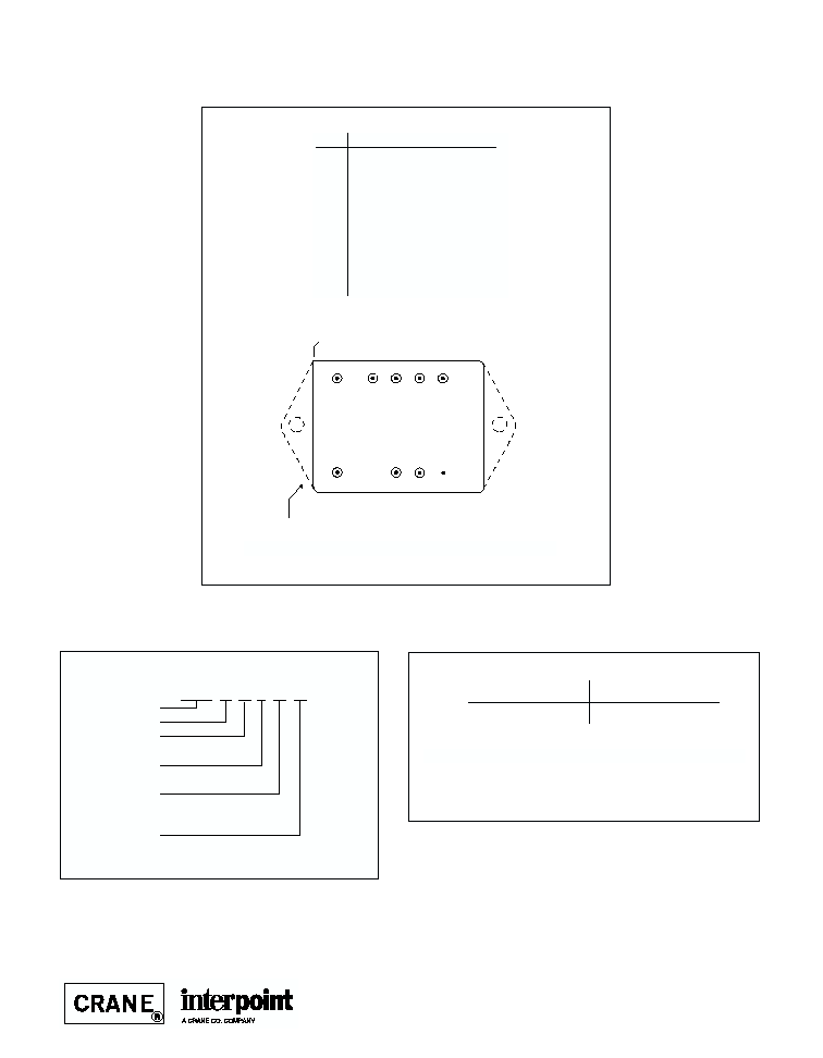
BOTTOM VIEW
MHF+ SINGLE AND DUAL
NON-FLANGED OR FLANGED
Dot on top of cover
indicates pin one.
Dotted line outlines flanged package option.
1
2
3
4
5
8
7
6
For exact specifications for an SMD product, refer to the SMD
drawing. Call your Interpoint representative for status on the
MHF+ SMD releases which are "in process". SMDs can be
downloaded from
http://www.dscc.dla.mil/programs/smcr
See pages 9 and 10 for dimensions.
Flanged SMDs have the suffix HZC instead of HXC.

7
MHF+ SERIES
SINGLE AND DUAL
15 WATT
DC/DC C
ONVERTERS
Typical Performance Curves: 25∞C Tc , 28 VDC Vin, 100% load, free run, unless otherwise specified.
F
IGURE
6
F
IGURE
8
OUTPUT POWER (Watts)
MHF+2805D EFFICIENCY
E
F
F
IC
IE
N
C
Y
(
%
)
40
90
80
70
60
50
2
4
6
8
10
12
40V
28V
16V
OUTPUT POWER (Watts)
MHF+2815D EFFICIENCY
E
F
F
IC
IE
N
C
Y
(
%
)
40
90
80
70
60
50
2
4
6
8
10
12
14
40V
28V
16V
OUTPUT POWER (Watts)
MHF+2805S EFFICIENCY
E
F
F
IC
IE
N
C
Y
(
%
)
40
90
80
70
60
50
2
4
6
8
10
12
16V
28V
40V
F
IGURE
3
OUTPUT POWER (Watts)
MHF+2812S EFFICIENCY
E
F
F
IC
IE
N
C
Y
(
%
)
40
90
80
70
60
50
2
4
6
8
10
12
14
16V
40V
28V
15
F
IGURE
4
OUTPUT POWER (Watts)
MHF+2812D EFFICIENCY
E
F
F
IC
IE
N
C
Y
(
%
)
40
90
80
70
60
50
2
4
6
8
10
12
14
40V
28V
16V
15
F
IGURE
7
F
IGURE
5
OUTPUT POWER (Watts)
MHF+2815S EFFICIENCY
E
F
F
IC
IE
N
C
Y
(%
)
40
90
80
70
60
50
2
4
6
8
10
12
14
16V
40V
15
28V
FREQUENCY (kHz)
MHF+ SERIES AUDIO REJECTION
A
T
T
E
N
U
A
T
IO
N
(d
B
)
≠100
0.1
1
10
100
≠90
≠80
≠70
≠60
≠50
≠40
≠20
≠10
0
≠30
F
IGURE
9
1ms/div
16V TO 40V
MHF+2805S STEP LINE RESPONSE
5
0
0
m
V
/d
iv
.
VIN
2
0
V
/d
iv
.
VOUT
F
IGURE
10
F
IGURE
11
50
µs/div
50% 100%
MHF+2805S STEP LOAD RESPONSE
100mV/div.
50% to 100%
100% to 50%

MHF+ SERIES
SINGLE AND DUAL
15 WATT
DC/DC C
ONVERTERS
8
Typical Performance Curves: 25∞C Tc , 28 VDC Vin, 100% load, free run, unless otherwise specified.
F
IGURE
18
F
IGURE
20
POSITIVE OUTPUT LOAD (% OF TOTAL LOAD)
≠V
OUT
WITH SHIFT IN LOAD BALANCE
CROSS REGULATION
≠
V
OUT
V
O
L
T
A
G
E
C
H
A
N
G
E
(
%
)
≠10
100
0
20
40
60
80
≠5
0
5
10
2812D
2815D
2805D
OUTPUT POWER (Watts)
50 mV DROP
LOW LINE DROPOUT VS. LOAD
IN
P
U
T
V
O
L
T
A
G
E
(
V
o
lts
)
10
11
12
13
14
15
14
15
16
MHF+2812S&D
MHF+2815S&D
MHF+2805S&D
13
12
50
µs/div
50% 100%
MHF+2815D +V
OUT
STEP LOAD RESPONSE
100mV/div.
50% to 100%
100% to 50%
PO= 7.5 W
F
IGURE
15
50
µs/div
20% 100%
MHF+2815D +VOUT STEP LOAD RESPONSE
1
0
0
m
V
/d
iv
.
20% to 100%
100% to 20%
PO= 7.5 W
F
IGURE
16
OUTPUT LOAD (%)
COND. A: 50% LOAD +V; 50% to 10% ≠V
COND. B: 50% LOAD ≠V; 50% to 10% +V
MHF+2805D/MHF+2812D/MHF+2815D
CROSS REGULATION
≠
V
O
U
T
V
O
L
T
A
G
E
C
H
A
N
G
E
(%
)
≠10
0
10
10
20
30
40
50
≠8
≠6
≠4
≠2
2
4
6
8
2815D
2812D
2812D
COND B
COND A
2805D
2805D
F
IGURE
19
F
IGURE
17
2 ms/div
MHF+2815D TURN-ON INTO FULL LOAD
2
0
V
/d
iv
.
VIN
5
V
/d
iv
.
+VOUT
≠VOUT
F
IGURE
12
F
IGURE
14
200
µs/div
10% 100%
MHF+2805S STEP LOAD RESPONSE
100mV/div.
10% to 100%
100% to 10%
1 ms/div
16V TO 40V
MHF+2815D STEP LINE RESPONSE
2
0
0
m
V
/d
iv
.
VIN
2
0
V
/d
iv
.
+VOUT
2 ms/div
MHF+2805S TURN-ON INTO FULL LOAD
1V/div.
VIN
20V/div.
VOUT
POUT= 12W
F
IGURE
13

9
DC/DC C
ONVERTERS
MHF+ SERIES
SINGLE AND DUAL
15 WATT
Note: Although every effort has been made to render the case drawings at actual size, variations in the printing process may cause some distortion. Please refer
to the numerical dimensions for accuracy.
CASE E
BOTTOM VIEW
See Figure 22
for pin configurations.
Squared corner and dot on top
of case indicate pin one.
1.460 max
(37.08)
1.130 max
(28.70)
Materials
Header Cold Rolled Steel/Nickel/Gold
Cover Kovar/Nickel
(SMHF Series
Cold Rolled Steel/Nickel/Gold)
Pins #52
alloy/Gold
compression glass seal
Case dimensions in inches (mm)
Tolerance
±0.005 (0.13) for three decimal places
±0.01 (0.3) for two decimal places
unless otherwise specified
CAUTION
Heat from reflow or wave soldering may damage
the device. Solder pins individually with heat
application not exceeding 300
∞C for 10 seconds
per pin.
F
IGURE
21: C
ASE
E M
AXIMUM
D
IMENSIONS
0.000
0.205
(5.21)
0.505
(12.83)
0.705
(17.91)
0.905
(22.99)
1.105
(28.07)
0.330 max
(8.38)
0.000
0.25 (6.35)
0.000
0.160
(4.06)
0.960
(24.38)
1
2
3
4
5
0.030 dia.
(0.76)
8
7
6
MHF+ Series Single and Dual: Screening ≠ Standard, ES, or 883
BOTTOM VIEW CASE E1
0.330 max
(8.38)
0.000
0.25 (6.35)
Projection Weld
Seam Seal
Squared corner and dot on top
of case indicate pin one.
F
IGURE
22: C
ASE
E1

10
DC/DC C
ONVERTERS
MHF+ SERIES
SINGLE AND DUAL
15 WATT
Materials
Header Cold Rolled Steel/Nickel/Gold
Cover
MHF+ Series and FMH Filter
Kovar/Nickel
SMHF
Cold Rolled Steel/Nickel
Pins
#52 alloy (all cases)
compression glass seal
Case dimensions in inches (mm)
Tolerance
±0.005 (0.13) for three decimal places
±0.01 (0.2) for two decimal places
unless otherwise specified
CASE G
BOTTOM VIEW
Flanged package
See Figure 24
for pin configuration
2.005 max
(50.93)
1.130 max
(28.70)
Squared corner and dot on top
of case indicate pin one.
CAUTION
Heat from reflow or wave soldering may damage
the device. Solder pins individually with heat
application not exceeding 300
∞C for 10 seconds
per pin.
Flange Thickness: 0.047 (1.19)
F
IGURE
23: C
ASE
G M
AXIMUM
D
IMENSIONS

11
DC/DC C
ONVERTERS
MHF+ SERIES
SINGLE AND DUAL
15 WATT
1.590 (40.39)
0.128 dia
(3.25)
0.030 dia.
(0.76)
Flanged cases: Designator "F" required in Case Option position of model number
MHF+ Series Single and Dual: Screening ≠ Standard, ES, or 883
BOTTOM VIEW CASE G1
0.000
0.205 (5.21)
0.505 (12.83)
0.705 (17.91)
0.905 (22.99)
1.105 (28.07)
0.000
0.160
(4.06)
0.960
(24.38)
1
2
3
4
5
8
7
6
0.140 (3.56)
0.560
(14.22)
0.330 max.
(8.38)
0.000
0.25 (6.35)
0.330 max.
(8.38)
0.000
0.25 (6.35)
Squared corner and dot on top
of case indicate pin one.
Projection Weld
Seam Seal
F
IGURE
24: C
ASE
G1

12
DC/DC C
ONVERTERS
MHF+ SERIES
SINGLE AND DUAL
15 WATT
TEST
STANDARD
/ES
/883 (Class H)*
PRE-CAP INSPECTION
Method 2017, 2032
yes
yes
yes
TEMPERATURE CYCLE (10 times)
Method 1010, Cond. C, -65∞C to 150∞C
no
no
yes
Method 1010, Cond. B, -55∞C to 125∞C
no
yes
no
CONSTANT ACCELERATION
Method 2001, 3000 g
no
no
yes
Method 2001, 500 g
no
yes
no
BURN-IN
Method 1015, 160 hours at 125∞C
no
no
yes
96 hours at 125∞C case (typical)
no
yes
no
FINAL ELECTRICAL TEST MIL-PRF-38534, Group A
Subgroups 1 through 6: -55∞C, +25∞C, +125∞C
no
no
yes
Subgroups 1 and 4: +25∞C case
yes
yes
no
HERMETICITY TESTING
Fine Leak, Method 1014, Cond. A
no
yes
yes
Gross Leak, Method 1014, Cond. C
no
yes
yes
Gross Leak, Dip (1 x 10
-3
)
yes
no
no
FINAL VISUAL INSPECTION
Method 2009
yes
yes
yes
Test methods are referenced to MIL-STD-883 as determined by MIL-PRF-38534.
*883 products are built with element evaluated components and are 100% tested and guaranteed over the full military temperature
range of ≠55∞C to +125∞C.
T
ABLE
1: E
NVIRONMENTAL
S
CREENING
21621-001-DTS Rev B This revision supercedes all previous releases.
All technical information is believed to be accurate, but no responsibility is
assumed for errors or omissions. Interpoint reserves the right to make changes in
products or specifications without notice. MHF+ Series is a trademark of Interpoint.
Copyright © 1999-2000 Interpoint. All rights reserved.
Contact Information:
Interpoint Headquarters USA
Phone:
1-800-822-8782
+425-882-3100
Email:
power@intp.com
www.interpoint.com
Interpoint UK
Phone:
+44-1252-815511
Email:
poweruk@intp.com
Interpoint France
Phone:
+33-134285455
Email:
powerfr@intp.com

1
Size (max.): Non flanged, case E2, 1.460 x 1.130 x 0.330 inches (37.08 x 28.70 x 8.38 mm)
Flanged , case G2, 2.005 x 1.130 x 0.330 inches (50.93 x 28.70 x 8.38 mm)
See Figures 13 - 16 for dimensions.
Weight:
32 grams maximum.
Screening: Standard, ES, or 883 (Class H). See Table 1 for screening options.
DESCRIPTION
Interpoint's MHF+ SeriesTM Triple DC/DC converters provide a wide
input voltage range of 16 to 48 VDC delivering 15 watts of total
output power with output voltages of +5 and ±12 or +5 and ±15
VDC. The main output, +5 VDC, will supply up to 7.5 watts and the
auxiliaries will supply up to 7.5 watts of combined power. Full power
operation at -55∞ C to +125∞C plus the ability to withstand transients
of up to 80 V for up to 120 milliseconds make these converters an
ideal choice for your high reliability systems.
C
ONVERTER
D
ESIGN
MHF+ Triple Series of DC/DC converters incorporate dual-phase,
phase-shifted technology with a continuous flyback topology. This
design eliminates a minimum load requirement on the main output
and eliminates cross regulation effects between the main output
voltage and the auxiliary output voltages. The phase-shifted design
offers a further benefit in reduced input and output ripple.
I
NHIBIT
F
UNCTION
An open collector, TTL compatible, inhibit terminal (pin 1) provides
shut-down and start-up control. Applying a logic level low (<0.8 V),
referenced to input common, will disable the output of the converter.
When inhibited input current is reduced to 5 mA or less and there is
no generation of switching noise. The inhibit terminal typically sinks
3 mA when the converter is inhibited.
Leaving the terminal open or pulling it high will enable the converter.
Use an open collector interface for logic high voltages of up to 11
volts. (Refer to Figure 2 for a connection diagram.) An open collector
interface is not required if the logic high is in excess of the open
circuit voltage of the inhibit terminal, 11 volts, but less than 40 volts.
S
OFT
S
TART
F
EATURE
The soft-start feature provides a controlled 20 milliseconds turn-on
to minimize inrush current and reduce overshoot at initial start-up or
when inhibit is released.
S
YNCHRONIZATION
To synchronize the converter's switching frequency to a system
clock apply the clock signal to the sync terminal (pin 7). When
multiple converters are powered from a single power source, asyn-
chronous (free run) operation will result in lower peak noise for
common spectral peaks, but synchronous operation will eliminate
any possibility of interference frequencies in the low audio band.
Source impedance of the signal should be less than 100 ohms and
the transition time should be less than 100 nanoseconds. The
capacitively coupled sync input will synchronize on a differential
signal of as low as 4 volts to as high as 10 volts. If the sync function
is not used, the terminal should be left open.
S
HORT
C
IRCUIT
P
ROTECTION
Internal current limiting circuitry protects all three outputs against
short circuits. When output power exceeds approximately 130% of
maximum output power, the output currents are limited. In addition,
separate current limiting circuitry protects each output individually
resulting in normal operation of either the main or the auxiliaries,
whichever is not in a shorted condition.
P
ACKAGING
MHF+ Triple converters are packaged in hermetically sealed metal
cases. MHF+ Triple converters can be purchased in a flanged or
non-flanged case. The flanged option provides increased heat dissi-
pation and also provides greater stability when mechanically
secured.
DC/DC C
ONVERTERS
28 V
OLT
I
NPUT
MHF+ SERIES TRIPLE
15 WATT
F
EATURES
∑ ≠55∞ to +125∞C operation
∑ 16 to 48 VDC input
∑ Fully Isolated
∑ Optocoupler feedback
∑ Fixed frequency 450 kHz
∑ Topology ≠ Current Mode Flyback
∑ Transient protection 80 V/120 ms
∑ Inhibit and sync functions
∑ Indefinite short circuit protection
∑ Undervoltage lockout
∑ Up to 76% efficiency
MODELS
VDC O
UTPUT
TRIPLE OUTPUT
+5 and ±12
+5 and ±15

RECOMMENDED OPERATING CONDITIONS
TYPICAL CHARACTERISTICS
ABSOLUTE MAXIMUM RATINGS
Input Voltage
∑ 16 to 48 VDC
Power Dissipation (Pd)
∑ 12 watts
Output Power
∑ 15 watts
Lead Soldering Temperature (10 sec per pin)
∑ 300∞C
Storage Temperature Range (Case)
∑ ≠65∞C to +150∞C
2
MHF+ SERIES TRIPLE
15 WATT
DC/DC C
ONVERTERS
Output Voltage Temperature Coefficient
∑ 150 ppm/∞C typical
Current Limit
∑ 130% typical
Isolation
∑ 100 megohm minimum at 500 V
Conversion Frequency
∑ Free run 375 minimum, 500 kHz maximum
∑ External sync range 400 to 600 kHz
Inhibit Pin Voltage (unit enabled)
∑ 10 V typical
Input Voltage Range
∑ 16 to 48 VDC continuous
∑ 80 V for up to 120 msec
Case Operating Temperature (Tc)
∑ ≠55∞C to +125∞C full power
∑ ≠55∞C to +135∞C absolute
Derating Output Power/Current
∑ Linearly from 100% at 125∞C to 0% at 135∞C
SYNC AND INHIBIT
Sync 400 to 600 kHz
∑ Duty cycle 40% to 60%
∑ Logic low 0.8 V max
∑ Logic high 4.5 V min, 10.0 V max
∑ If not used, leave unconnected
∑ Referenced to input common
Inhibit: TTL Open Collector
∑ Logic low (output disabled)
Logic low voltage
0.8 V max
Inhibit pin current 3.0 typ, 5.0 max
∑ Referenced to input common
Logic high (output enabled)
Open collector
Unconnected or 11 to 40 V
PWM CM
CONTROLLER
0
∞
180
∞
PWM CM
CONTROLLER
INPUT
COMMON
FEEDBACK ISOLATOR
FEEDBACK ISOLATOR
OUTPUT
COMMON
+ AUX.
OUTPUT
≠AUX.
OUTPUT
POSITIVE
INPUT
SYNC
+5 OUTPUT
F
IGURE
1: B
LOCK
D
IAGRAM

3
MHF+ SERIES TRIPLE
15 WATT
DC/DC C
ONVERTERS
Electrical Characteristics: 25∞C Tc, 28 VDC Vin, 100% load, free run, unless otherwise specified.
MHF+28512T
MHF+28515T
PARAMETER
CONDITION
MIN
TYP
MAX
MIN
TYP
MAX
UNITS
OUTPUT VOLTAGE
MAIN
4.95
5.0
5.05
4.925
5.0
5.05
+ AUXILIARY
11.64
12.0
12.36
14.55
15.0
15.45
VDC
≠ AUXILIARY
11.64
12.0
12.36
14.55
15.0
15.45
OUTPUT CURRENT
1
MAIN
0
--
1.5
0
--
1.5
+ AUXILIARY
--
--
0.416
--
--
0.333
A
≠ AUXILIARY
--
--
0.416
--
--
0.333
TOTAL
--
--
2.125
--
--
2.0
OUTPUT POWER
2
MAIN
--
--
7.5
--
--
7.5
+ AUXILIARY
--
--
5
--
--
5
W
≠ AUXILIARY
--
--
5
--
--
5
TOTAL
--
--
15
--
--
15
OUTPUT RIPPLE
10 kHz to 2 MHz MAIN
--
20
75
--
20
75
VOLTAGE
10 kHz to 2 MHz ± AUXILIARY
--
30
90
--
30
112
mV p-p
LINE REGULATION
3
MAIN
--
25
75
--
25
75
mV
V
IN
= MIN. TO MAX.
±AUXILIARY
--
120
240
--
150
300
LOAD REGULATION
3, 4
MAIN
--
25
60
--
25
60
mV
± AUXILIARY
--
120
240
--
150
300
CROSS REGULATION
5
≠ AUXILIARY
--
--
1200
--
--
1500
mV
INPUT VOLTAGE
CONTINUOUS
16
28
48
16
28
48
VDC
TRANSIENT 120 ms
--
--
80
--
--
80
V
INPUT CURRENT
NO LOAD
3
--
20
35
--
20
35
FULL LOAD
--
705
724
--
705
724
mA
INHIBITED
3
--
3
5
--
3
5
INPUT RIPPLE CURRENT
10 kHz to 10 MHz
--
20
50
--
20
50
mA p-p
EFFICIENCY
74
76
--
74
76
--
%
LOAD FAULT
6
POWER DISSIPATION
MAIN
3
--
--
12
--
--
12
W
±AUXILIARY
--
--
12
--
--
12
STEP LOAD
TRANSIENT
RESPONSE
3, 7, 8
MAIN
--
--
850
--
--
850
mV pk
± AUXILIARY
--
--
750
--
--
750
RECOVERY MAIN
--
5
8
--
5
8
ms
RECOVERY ±AUX.
--
2
3
--
2
3
START-UP
3,
DELAY EACH OUTPUT
--
10
25
--
10
25
ms
Notes
1. The sum of the 12 volt auxiliary output currents may not exceed 625 mA.
The sum of the 15 volt auxiliary output currents may not exceed 500 mA.
2. The sum of the auxiliary output power may not exceed 7.5 watts.
3. Case temperature ≠55∞C to +125∞C.
4. Load regulation for the +5 is specified at 0.0 to 1.5 A with the aux. both held
at 3.76 W (313 mA for the ±12, 250 mA for the ±15). Load regulation for the
aux. is specified as both aux. from 0.0 to 3.76 W (313 mA for ±12, 250 mA
for ±15) at the same time with the +5 held at 1.5 A.
5. Cross regulation only occurs between the two auxiliaries and is measured on
≠aux. +5 is held constant at 1.0 A. Cross regulation is specified for two
conditions:
Negative aux.= 3.76 W; positive aux.= 0.37 W to 3.76 W.
Negative aux. = 0.37 W to 3.76 W; positive aux. = 3.76 W.
6. Load fault = <0.05
.
7. Transition time is 2 ≠ 10 µs.
8. Time to settle to within 1% of Vout final value.

Positive Input
1
5
28V
Input Common
FMH-461
EMI FILTER
Positive Output
Output Common
3
Positive Input
9
8
Input Common
MHF+ TRIPLE
2
4
Case*
*The case ground connection should be as low an impedance as possible to minimize EMI.
Direct contact of baseplate to chassis ground provides the lowest impedance.
Chassis Ground
6
+5
Load
Positive Input
9
7
1
8
2
4
5
28V
Sync In
Inhibit
Input Common
+5 Output
Output Common
≠ Aux. Output
+ Aux.
Load
3
≠ Aux.
Load
+ Aux. Output
0.01 F
5.1k
9
1
8
200 pF
3.9 K
10 K
INHIBIT
MHF+ Triple
INPUT
COMMON
POSITIVE INPUT
10 k
1N4148
2N3501
4
MHF+ SERIES TRIPLE
15 WATT
DC/DC C
ONVERTERS
CONNECTION DIAGRAMS
F
IGURE
2: I
NHIBIT
I
NTERFACE
F
IGURE
3: AC C
OUPLING OF
S
YNC
S
IGNAL
F
IGURE
4: EMI F
ILTER
C
ONNECTION
If the sync terminal ([pin 7) is not used, it must be left floating.
The ac coupling shown will prevent sync signal failure.
SMD NUMBERS
PIN OUT
MHF+ 28 512 T F / ES
Base Model
Input Voltage
Output Voltage
Screening
Number of Outputs
(T = triple)
(Main and aux. Vout)
Case Option
(Non-flanged case has no designator in
this position)
(Standard screening has no designator
in this position.)
5
MHF+ SERIES TRIPLE
15 WATT
DC/DC C
ONVERTERS
MODEL NUMBERING KEY
Pin
Description
1
Inhibit
2
Main (+5 V) Output
3
Output Common
4
Positive Auxiliary Output
5
Negative Auxiliary Output
6
Case Ground
7
Sync In
8
Input Common
9
Positive Input
If Sync is not used, leave it unconnected.
F
IGURE
5: P
IN
O
UT
B
OTTOM
V
IEW
S
TANDARD
M
ICROCIRCUIT
D
RAWING
(SMD)
5962-9560101HXC
5962-9560201HXC
MHF+
S
IMILAR
P
ART
MHF+28512T/883
MHF+28515T/883
Dotted line outlines flanged package option.
1
2
3
4
5
9
8
6
7
Squared corner and dot on top
of package indicate pin one.
BOTTOM VIEW
MHF+ Triple
For exact specifications for an SMD product, refer to the SMD drawing. SMDs
can be downloaded from
http://www.dscc.dla.mil/programs/smcr
Refer to Figures 13 - 16 for dimensions.
Flanged SMDs have the suffix HZC instead of HXC.

6
MHF+ SERIES TRIPLE
15 WATT
DC/DC C
ONVERTERS
Typical Performance Curves: 25∞C Tc , 28 VDC Vin, 100% load, free run, unless otherwise specified.
F
IGURE
9
F
IGURE
11
MHF+28512T TURN ON INTO FULL LOAD
MAIN
5 ms / div.
+5 VDC
2 V / div.
MHF+28515T has a similar response
10 V / div.
VIN
INPUT
GND
+5
GND
MHF+28512T TURN ON INTO FULL LOAD
AUXILIARIES
5 ms / div.
≠12 VDC
5 V / div.
+12 VDC
MHF+28515T has a similar response
10 V / div.
VIN
16
EFFICIENCY
55
80
60
65
70
75
4
6
8
10
12
14
16 V
28 V
48 V
2
MHF+28512T EFFICIENCY
OUTPUT POWER (W)
F
IGURE
6
16
EFFICIENCY
55
80
60
65
70
75
2
4
6
8
10
12
14
16 V
48 V
MHF+28515T EFFICIENCY
OUTPUT POWER (W)
28 V
F
IGURE
7
MHF+28512T TURN ON INTO FULL LOAD
MAIN
5 ms / div.
+5 VDC
2 V / div.
MHF+28515T has a similar response
10 V / div.
VIN
INPUT
GND
+5
GND
F
IGURE
10
F
IGURE
8
MHF+28512T has a similar response
MHF+ 28515T STEP LINE RESPONSE
500 mV / div.
5 ms / div.
≠15 VDC
±15 = 250 mA EACH, +5 = 1.5 A
200 mV / div.
INPUT V: 16 TO 40 VDC,
+15 VDC
5 VDC
MAXIMUM OUTPUT POWER (W)
INPUT VOLTAGE
LOW LINE DROPOUT
MHF+28515T
MHF+28512T
11.5
11
10.5
9.5
9
8.5
10
2
4
6
8
10
12
14
16
F
IGURE
12

7
DC/DC C
ONVERTERS
Note: Although every effort has been made to render the case drawings at actual size, variations in the printing process may cause some distortion. Please refer
to the numerical dimensions for accuracy.
CASE E
BOTTOM VIEW
See Figure 14
for pin configurations.
Squared corner and dot on top
of case indicate pin one.
1.460 max
(37.08)
1.130 max
(28.70)
Materials
Header Cold
Rolled
Steel/Nickel/Gold
Cover Kovar/Nickel
(SMHF
Series
Cold
Rolled
Steel/Nickel/Gold)
Pins
#52 alloy/Gold
compression glass seal
Case dimensions in inches (mm)
Tolerance
±0.005 (0.13) for three decimal places
±0.01 (0.3) for two decimal places
unless otherwise specified
CAUTION
Heat from reflow or wave soldering may damage
the device. Solder pins individually with heat
application not exceeding 300
∞C for 10 seconds
per pin.
F
IGURE
13: C
ASE
E M
AXIMUM
D
IMENSIONS
0.000
0.205
(5.21)
0.505
(12.83)
0.705
(17.91)
0.905
(22.99)
1.105
(28.07)
0.000
0.160
(4.06)
0.960
(24.38)
0.030 dia.
(0.76)
MHF+ Series Triple: Screening ≠ Standard, ES, or 883
1
2
3
4
5
8
7
6
9
BOTTOM VIEW CASE E2
0.330 max
(8.38)
0.000
0.25 (6.35)
0.330 max
(8.38)
0.000
0.25 (6.35)
Projection Weld
Seam Seal
Squared corner and dot on top
of case indicate pin one.
F
IGURE
14: C
ASE
E2
MHF+ SERIES TRIPLE
15 WATT

8
DC/DC C
ONVERTERS
Note: Although every effort has been made to render the case drawings at actual size, variations in the printing process may cause some distortion. Please refer
to the numerical dimensions for accuracy.
Materials
Header Cold Rolled Steel/Nickel/Gold
Cover MHF+ Series and FMH Filter
Kovar/Nickel
Pins
#52 alloy (all cases)
compression glass seal
Case dimensions in inches (mm)
Tolerance
±0.005 (0.13) for three decimal places
±0.01 (0.2) for two decimal places
unless otherwise specified
CASE G
BOTTOM VIEW
Flanged package
See Figure 16
for pin configuration
2.005 max
(50.93)
1.130 max
(28.70)
Squared corner and dot on top
of case indicate pin one.
CAUTION
Heat from reflow or wave soldering may damage
the device. Solder pins individually with heat
application not exceeding 300
∞C for 10 seconds
per pin.
Flange Thickness: 0.047 (1.19)
F
IGURE
15: C
ASE
G M
AXIMUM
D
IMENSIONS
1.590 (40.39)
0.128 dia
(3.25)
0.030 dia.
(0.76)
Flanged case: Designator (F) required in Case Option position of model number.
MHF+ Series Triple: Screening ≠ Standard, ES, or 883
BOTTOM VIEW CASE G2
0.000
0.205 (5.21)
0.505 (12.83)
0.705 (17.91)
0.905 (22.99)
1.105 (28.07)
0.000
0.160
(4.06)
0.960
(24.38)
1
2
3
4
5
9
8
6
7
0.140 (3.56)
0.560
(14.22)
0.330 max.
(8.38)
0.000
0.25 (6.35)
0.330 max.
(8.38)
0.000
0.25 (6.35)
Projection Weld
Seam Seal
Squared corner and dot on top
of case indicate pin one.
F
IGURE
17: C
ASE
G2
MHF+ SERIES TRIPLE
15 WATT

9
DC/DC C
ONVERTERS
MHF+ SERIES TRIPLE
15 WATT
TEST
STANDARD
/ES
/883 (Class H)*
PRE-CAP INSPECTION
Method 2017, 2032
yes
yes
yes
TEMPERATURE CYCLE (10 times)
Method 1010, Cond. C, -65∞C to 150∞C
no
no
yes
Method 1010, Cond. B, -55∞C to 125∞C
no
yes
no
CONSTANT ACCELERATION
Method 2001, 3000 g
no
no
yes
Method 2001, 500 g
no
yes
no
BURN-IN
Method 1015, 160 hours at 125∞C
no
no
yes
96 hours at 125∞C case (typical)
no
yes
no
FINAL ELECTRICAL TEST MIL-PRF-38534, Group A
Subgroups 1 through 6: -55∞C, +25∞C, +125∞C
no
no
yes
Subgroups 1 and 4: +25∞C case
yes
yes
no
HERMETICITY TESTING
Fine Leak, Method 1014, Cond. A
no
yes
yes
Gross Leak, Method 1014, Cond. C
no
yes
yes
Gross Leak, Dip (1 x 10
-3
)
yes
no
no
FINAL VISUAL INSPECTION
Method 2009
yes
yes
yes
Test methods are referenced to MIL-STD-883 as determined by MIL-PRF-38534.
*883 products are built with element evaluated components and are 100% tested and guaranteed over the full military temperature
range of ≠55∞C to +125∞C.
T
ABLE
1: E
NVIRONMENTAL
S
CREENING
Contact Information:
www.interpoint.com
Interpoint Headquarters USA
Phone:
1-800-822-8782
+425-882-3100
Email:
power@intp.com
Interpoint UK
Phone:
+44-1252-815511
Email:
poweruk@intp.com
Interpoint France
Phone:
+33-134285455
Email:
powerfr@intp.com
21623-002-DTS Rev B This revision supercedes all previous releases.
All technical information is believed to be accurate, but no responsibility is
assumed for errors or omissions. Interpoint reserves the right to make changes in
products or specifications without notice. MHF+ Series is a trademark of Interpoint.
Copyright © 1995 - 1999 Interpoint. All rights reserved.