 | –≠–ª–µ–∫—Ç—Ä–æ–Ω–Ω—ã–π –∫–æ–º–ø–æ–Ω–µ–Ω—Ç: MHV2815S | –°–∫–∞—á–∞—Ç—å:  PDF PDF  ZIP ZIP |

1
Size (max.): Non flanged Single and dual output models, case H2, 2.125 x 1.125 x 0.400 inches (53.98 x 28.58 x 10.16 mm)
Triple output models, case F1, 1.950 x 1.350 x 0.405 inches (49.53 x 34.29 x 10.29 mm)
Flanged Single and dual output models, case K3, 2.910 x 1.125 x 0.400 inches (73.91 x 28.58 x 10.16 mm)
Triple output models, case J1, 2.720 x 1.350 x 0.405 inches (69.09 x 34.29 x 10.29 mm)
See Section B8, cases H2, F1, K3, and J1 for dimensions.
Weight:
60 grams maximum.
Screening: Standard, ES, or 883 (Class H). See Section C2 for
screening options, see Section A5 for ordering information.
DESCRIPTION
Interpoint's MHV SeriesTM of DC/DC converters offer a wide input
voltage range of 16 to 50 VDC and a choice of nine different output
voltage configurations comprised of single, dual or triple outputs.
The converters will withstand transients of up to 80 V for up to 120
milliseconds while maintaining output voltages (with the exception of
the 12 volt single and dual outputs which will withstand transients up
to 75 volts and the 15 volt single and dual outputs which will with-
stand up to 60 volts). The MHV Series operates at a full 15 watts of
output power (10 watts for the 3.3 volt single output) over the mili-
tary temperature range of ≠55∞C to +125∞C while maintaining low
input and output noise.
C
ONVERTER
D
ESIGN
MHV Series DC/DC converters are switching regulators that use
continuous flyback conversion topology with a clock frequency of
approximately 600 kHz. MHV Series converters incorporate two
internal converters with one converter phase shifted 180∞ from the
other to create a dual phase/phase-shifted operation. Each of the
internal converters operates at approximately one-half of the clock
frequency. This proprietary technology eliminates cross regulation,
minimizes input ripple, greatly reduces output ripple and improves
efficiency. On the triple output models, this design provides
completely independent regulation with no cross regulation effect
between the main and auxiliary outputs and no minimum loading
required on the main output.
I
NHIBIT
F
UNCTION
Open collector TTL levels control the inhibit circuit. The converter is
enabled when the inhibit terminal is left unconnected or when the
inhibit terminal is connected to a voltage between 11.5 and 50 V.
When a low (0.8 V) is applied to the inhibit terminal the converter
shuts down, typically drawing 8.4 mA of input current. Inhibit
terminal resistance is 3.3 k ohms and draws 8.4 mA, typical.
S
YNCHRONIZATION
F
UNCTION
Applying an external signal of 40% to 60% duty cycle and 500 to
700 kHz will synchronize the converter to your system requirements.
Free run clock frequency is approximately 600 kHz. If not used, the
sync terminal must be left unconnected.
T
RIM
Single output converters feature a trim range of as low as 80% to
as high as 110% of Vout nominal, depending on the model. To trim
up, connect a resistor from output common (pin 4) to the trim
terminal (pin 3). To trim down, connect a resistor from the positive
output (pin 5) to the trim terminal (pin 3). See Figure 4 and trim
tables for more information.
U
NDERVOLTAGE
L
OCKOUT
An undervoltage lockout of approximately 7 VDC keeps system
current levels low during startup.
S
HORT
C
IRCUIT
P
ROTECTION
Under short circuit conditions of 130% or more of full load current,
the converter will protect itself by shutting down. Short circuit dura-
tion should be brief because power dissipation may cause internal
temperatures to rise rapidly. Restart is automatic upon removal of
the short circuit.
DC/DC C
ONVERTERS
28 V
OLT
I
NPUT
MHV SERIES
15 WATT
F
EATURES
∑ ≠55∞ to +125∞C operation
∑ 16 to 50 VDC input
∑ Fully Isolated
∑ Optocoupler feedback
∑ Fixed switching frequency
600 kHz typical,
∑ Topology ≠
Dual Single Ended Flybacks
∑ 80 V / 120 ms transient protection
(12 Vout single and dual to 75 V,
15 Vout single and dual to 60V)
∑ Inhibit and sync functions
∑ Trim on single output models
∑ Up to 84% efficiency
∑ Low output noise
MODELS
VDC O
UTPUT
SINGLE
3.3
5
12
15
DUAL
±5
±12
±15
TRIPLE
+5 & ±12
+5 & ±15
TYPICAL CHARACTERISTICS
SYNC AND INHIBIT
RECOMMENDED OPERATING CONDITIONS
ABSOLUTE MAXIMUM RATINGS
Input Voltage
∑ 16 to 50 VDC
Output Power
∑ 15 watts (10 watts MHV283R3S)
Lead Soldering Temperature (10 sec per lead)
∑ 300∞C
Storage Temperature Range (Case)
∑ ≠65∞C to +150∞C
2
MHV SERIES
15 WATT
DC/DC C
ONVERTERS
Output Voltage Temperature Coefficient
∑ 100 ppm/∞C typical
Undervoltage Lockout
∑ 7 V input typical
Current Limit
∑ 130% of full load typical at 25∞C
Isolation
∑ 100 megohm minimum at 500 V
Audio Rejection
∑ 30 dB typical
Conversion (Switching) Frequency
∑ Free run mode 300 kHz
typical 245 kHz. min, 355 kHz. max
Clock Frequency
∑ External sync range 500 to 700 kHz.
Inhibit Pin Voltage (unit enabled)
∑ 11 V typical
Input Voltage Range
∑ 16 to 50 VDC continuous
∑ Transient: see Electrical Characteristics tables
Case Operating Temperature (Tc)
∑ ≠55∞C to +125∞C full power
∑ ≠55∞C to +130∞C absolute
Derating Output Power/Current
∑ Linearly from 100% at 125∞C to 0% at 130∞C
Electrical Characteristics: 25∞C Tc, 28 VDC Vin, 100% load, free run, unless otherwise specified.
Sync In (500 to 700 kHz)
∑ Duty cycle 40% min, 60% max
∑ Logic low 0.8 V max
∑ Logic high 4.5 V min, 10 V max
∑ Referenced to input common
∑ If not used, leave unconnected
Inhibit TTL Open Collector
∑ Logic low (output disabled)
Logic low voltage
0.8 V
Inhibit pin current
8.4 mA typical, 10 mA maximum
∑ Referenced to input common
∑ Logic high (output enabled)
Open collector
Unconnected or 11.5 to 50 V
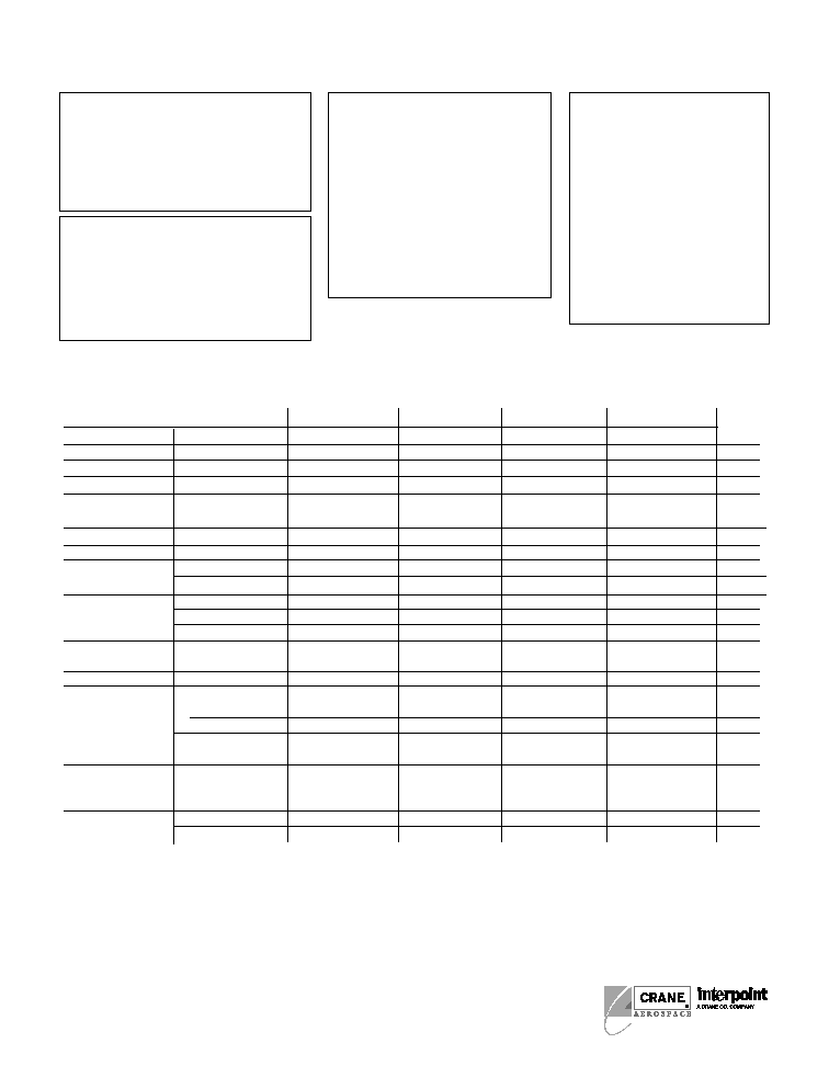
SINGLE OUTPUT MODELS
MHV283R3S
MHV2805S
MHV2812S
MHV2815S
PARAMETER
CONDITIONS
MIN TYP MAX
MIN
TYP
MAX
MIN
TYP
MAX
MIN
TYP
MAX
UNITS
OUTPUT VOLTAGE
3.27
3.30
3.33
4.95
5.00
5.05
11.88
12.00 12.12
14.85 15.00
15.15
VDC
OUTPUT CURRENT
V
IN
= 16 to 50 VDC
0
--
3.03
0
--
3.0
0
--
1.25
0
--
1.0
A
OUTPUT POWER
V
IN
= 16 to 50 VDC
0
--
10
0
--
15
0
--
15
0
--
15
W
OUTPUT RIPPLE
10 kHz - 2 MHz
VOLTAGE
Tc = ≠55∞C to +125∞C
--
5
60
--
10
60
--
7
60
--
5
60
mV p-p
LINE REGULATION
V
IN
= 16 to 50 VDC
--
0
20
--
0
20
--
0
20
--
0
20
mV
LOAD REGULATION
NO LOAD TO FULL
--
15
45
--
15
40
--
5
35
--
5
40
mV
INPUT VOLTAGE
CONTINUOUS
16
28
50
16
28
50
16
28
50
16
28
50
VDC
NO LOAD TO FULL
TRANSIENT 120 ms
--
--
80
--
--
80
--
--
75
--
--
60
V
INPUT CURRENT
NO LOAD
--
23
45
--
29
52
--
26
51
--
28
57
mA
FULL LOAD
--
489
518
--
687
724
--
638
678
--
638
687
mA
INHIBITED
--
8.4
10
--
8.4
10
--
8.4
10
--
8.4
10
mA
INPUT RIPPLE
10 kHz - 20 MHz
CURRENT
1
Tc = ≠55∞C to +125∞C
--
10
50
--
10
50
--
10
50
--
10
50
mA pp
EFFICIENCY
69
73
--
74
78
--
79
84
--
78
84
--
%
LOAD FAULT
2
POWER DISSIPATION
SHORT CIRCUIT
2
--
--
9.5
--
--
11
--
--
11
--
--
10.5
W
RECOVERY
--
--
20
--
--
20
--
--
20
--
--
20
ms
OUTPUT CURRENT
TRIP POINT
3.97
--
--
3.93
--
--
1.64
--
--
1.31
--
--
A
STEP LOAD
50% ≠ 100% ≠ 50%
RESPONSE
3
TRANSIENT
--
--
250
--
--
300
--
--
300
--
--
350
mV pk
RECOVERY
--
--
700
--
--
1500
--
--
900
--
--
700
µs
START-UP
DELAY
--
5
20
--
5
20
--
5
20
--
5
20
ms
0 TO 28 V
IN
OVERSHOOT
--
50
100
--
0
50
--
0
120
--
0
150
mV pk
Notes
1. Lin = 5.5 µH.
2. Load fault is a short circuit (<50 m
). Recovery is into a resistive load.
3. Load step transition
10 µs. Recovery = time to settle to within 1% of Vout final value.
4. Input step transition
10 µs. Recovery = time to settle to within 1% of Vout final value.

3
MHV SERIES
15 WATT
DC/DC C
ONVERTERS
Electrical Characteristics: 25∞C Tc, 28 VDC Vin, 100% load, free run, unless otherwise specified.
DUAL OUTPUT MODELS
MHV2805D
MHV2812D
MHV2815D
PARAMETER
CONDITIONS
MIN
TYP
MAX
MIN
TYP
MAX
MIN
TYP
MAX
UNITS
OUTPUT VOLTAGE
+V
OUT
4.95
5.00
5.05
11.88
12.00
12.12
14.85
15.00
15.15
VDC
≠V
OUT
4.95
5.00
5.05
11.88
12.00
12.12
14.85
15.00
15.15
OUTPUT CURRENT
V
IN
= 16 TO 50 VDC
--
--
±1.50
--
--
±0.625
--
--
±0.500
A
OUTPUT POWER
1
V
IN
= 16 TO 50 VDC
--
±7.5
15
--
±7.5
15
--
±7.5
15
W
OUTPUT RIPPLE
10 kHz- 2 MHz
VOLTAGE
Tc = ≠55∞C to +125∞C
+V
OUT
/ ≠V
OUT
--
15
120
--
10
60
--
20
80
mVp-p
LINE REGULATION
V
IN
= 16 TO 50 VDC ±V
OUT
--
0
20
--
0
20
--
0
20
mV
LOAD REGULATION
NO LOAD TO FULL ±V
OUT
--
5
40
--
5
40
--
5
40
mV
INPUT VOLTAGE
CONTINUOUS
16
28
50
16
28
50
16
28
50
VDC
NO LOAD TO FULL
TRANSIENT 120 msec
--
--
80
--
--
75
--
--
60
V
INPUT CURRENT
NO LOAD
--
18
25
--
30
40
--
35
45
FULL LOAD
--
670
705
--
634
670
--
635
670
mA
INHIBITED --
8.4
10
--
8.4
10
--
8.4
10
INPUT RIPPLE
10 kHz - 20 MHz
CURRENT
2
Tc = ≠55∞C to +125∞C
--
10
200
--
10
200
--
10
200
mA p-p
EFFICIENCY
76
80
--
80
85
--
80
84
--
%
LOAD FAULT
3
POWER DISSIPATION
SHORT CIRCUIT
--
--
9
--
--
10
--
--
10
W
RECOVERY
--
--
15
--
--
25
--
--
25
ms
OUTPUT CURRENT
TRIP POINT
1.97
--
--
0.819
--
--
0.655
--
--
A
STEP LOAD
50% ≠ 100% -- 50%
RESPONSE
4
± V
OUT
TRANSIENT
--
--
200
--
--
300
--
--
400
mV pk
RECOVERY
--
--
500
--
--
700
--
--
900
µs
START-UP
DELAY
--
5
12
--
10
18
--
12
20
ms
0 TO 28 V
IN
OVERSHOOT
--
0
50
--
0
120
--
0
150
mV pk
Notes
1. Up to 7.5 watts is available from either output.
2. Lin = 2 µH.
3. Load fault is a short circuit (<50 m
). Recovery is into a resistive load.
4. Load step transition
10 µs. Recovery = time to settle to within 1% of Vout final value.
5. Input step transition
10 µs. Recovery = time to settle to within 1% of Vout final value.

4
MHV SERIES
15 WATT
DC/DC C
ONVERTERS
Electrical Characteristics: 25∞C Tc, 28 VDC Vin, 100% load, free run, unless otherwise specified.
TRIPLE OUTPUT MODELS
MHV28512T
MHV28515T
PARAMETER
CONDITION
MIN
TYP
MAX
MIN
TYP
MAX
UNITS
OUTPUT VOLTAGE
MAIN
4.95
5.0
5.05
4.95
5.0
5.05
+ AUXILIARY
11.88
12.0
12.12
14.85
15.0
15.15
VDC
≠ AUXILIARY
11.82
12.0
12.18
14.77
15.0
15.23
OUTPUT CURRENT
1
MAIN
0
--
2.0
0
--
2.0
V
IN
= 16 TO 50
+ AUXILIARY
--
--
0.333
--
--
0.267
A
≠ AUXILIARY
--
--
0.333
--
--
0.267
TOTAL
--
--
2.416
--
--
2.333
OUTPUT POWER
2
MAIN
--
--
10
--
--
10
V
IN
= 16 TO 50
+ AUXILIARY
--
--
4
--
--
4
W
≠ AUXILIARY
--
--
4
--
_
4
TOTAL
--
--
15
--
--
15
OUTPUT RIPPLE
10 kHz to 2 MHz MAIN
--
5
30
--
10
35
VOLTAGE
10 kHz to 2 MHz ± AUXILIARY
--
5
30
--
10
35
mV p-p
LINE REGULATION
MAIN
--
0
20
--
0
20
V
IN
= MIN. TO MAX.
+AUXILIARY
--
1
35
--
5
35
mV
≠ AUXILIARY
--
1
35
--
5
35
LOAD REGULATION
MAIN
--
10
25
--
10
25
+AUXILIARY
--
10
45
--
15
55
mV
≠ AUXILIARY
--
10
65
--
15
80
CROSS REGULATION
3
CONDITION A
--
300
500
--
300
500
mV
≠ AUXILIARY
CONDITION B
--
400
700
--
400
700
INPUT VOLTAGE
CONTINUOUS
16
28
50
16
28
50
VDC
TRANSIENT 120 ms
--
--
80
--
--
80
INPUT CURRENT
NO LOAD
--
23
32
--
28
37
FULL LOAD
--
670
705
--
670
705
mA
INHIBITED
--
8.4
10
--
8.4
10
INPUT RIPPLE CURRENT
10 kHz to 10 MHz
--
10
40
--
15
40
mA p-p
EFFICIENCY
76
80
--
76
80
--
%
LOAD FAULT
4
SHORT CIRCUIT
POWER DISSIPATION
MAIN
--
--
9
--
--
9
W
W
± AUXILIARY
--
--
8
--
--
8
STEP LOAD RESPONSE
5, 6
TRANSIENT
MAIN
--
--
250
--
--
250
± AUXILIARY
--
--
500
--
--
500
mV
RECOVERY
MAIN
--
--
2.5
--
--
2.5
ms
± AUXILIARY
--
--
4
--
--
3.5
START-UP
6
0 TO 28 V
IN
DELAY EACH OUTPUT
--
5
12
--
5
12
ms
Notes
1. The sum of the 12 volt auxiliary output currents may not exceed 416 mA.
The sum of the 15 volt auxiliary output currents may not exceed 333 mA.
2. The sum of the auxiliary output power may not exceed 5 watts.
3. Cross regulation occurs between the two auxiliaries and is measured on ≠aux.
+5 is held constant at 2.0 A. Cross regulation is specified for two conditions:
A. Positive aux. = 2.5 W; negative aux. = 2.5 W to 0.5 W.
B. Negative aux. = 4 W to 1 W; positive aux. = 1 W to 4 W, simultaneous.
4. Load fault is a short circuit (<50 m
). Recovery is into a resistive load.
5. Load step transition
10 µs. Recovery = time to settle to within 1% of Vout
final value.
6. Input step transition
10 µs. Recovery = time to settle to within 1% of Vout
final value.
7. Lin = 5.5 µH.

TRIM ≠ SINGLE OUTPUT MODELS ONLY
Formula Values by Model
3.3V
5V
12V
15V
A
3.7
3.7
14
18.2
B
10
10
30
30
Positive
Input
0
o
180
o
Input
Common
Sync.
Positive
Output,
Main (+5)
Output
Common
Positive
Output,
Auxiliary
Negative
Output,
Auxiliary
Feedback Isolator
Feedback Isolator
PWM CM
Controller
PWM CM
Controller
Trim down: R
T
(k
) =
(
(V
o
≠ 2.5)
)
A ≠ B
V
o nominal
≠ V
0
Trim up:
R
T
(k
) =
(
2.5A
)
≠B
V
o ≠
V
o nominal
V
o
= desired output voltage
Positive Input
1
10
Input Common
MHV
2
4
Case*
*The case ground connection should be as low an impedance as possible to minimize EMI.
Direct contact of baseplate to chassis ground provides the lowest impedance.
Chassis Ground
6, 7, 8
Positive Input
1
5
28V
Input Common
FMC-461
or FMH-461
EMI FILTER
Positive Output
Output Common
3
M
ODEL
% V
OUT
N
OMINAL
110
106
102
95
90
80
MHV283R3S
18
36
128
4
n/a
n/a
MHV2805S
8
20
81
23
5
n/a
MHV2812S
n/a
19
116
177
67
11
MHV2815S
0.3
21
122
255
104
28
5
MHV SERIES
15 WATT
DC/DC C
ONVERTERS
DIAGRAMS
F
IGURE
1: MHV T
RIPLE
B
LOCK
D
IAGRAM
F
IGURE
3: EMI F
ILTER
C
ONNECTION
Positive Input
1
9
2
10
28V
Sync In
Inhibit (pin 8 on triple
output models)
Input Common
MHV
F
IGURE
4: MHV S
INGLE
O
UTPUT
T
RIM
Notes
If calculated result is a negative value, the desired output voltage is outside the allowed trim range.
Calculated values of R
T
are ±15%.
When trimming up, do not exceed the maximum output power.
When trimming down, do not exceed the maximum output current.
Calculated Trim
Quick Reference Trim Table
R
TRIM (
(R
T
) k ohms
3
TRIM
R
T
5
4
+V
O
OUTPUT
COMMON
MHV
SINGLE
OUTPUT
TRIM DOWN
TRIM UP
F
IGURE
2: T
YPICAL
C
ONNECTIONS