 | –≠–ª–µ–∫—Ç—Ä–æ–Ω–Ω—ã–π –∫–æ–º–ø–æ–Ω–µ–Ω—Ç: MTO2812T | –°–∫–∞—á–∞—Ç—å:  PDF PDF  ZIP ZIP |

MODELS
VDC O
UTPUT
B4-23
F
EATURES
∑ ≠55∞C to +85∞ C operation
∑ 9 to 16 or 16 to 36 VDC input
∑ Fully isolated
∑ Opto-coupler feedback
∑ Fixed frequency, 250 kHz typical
∑ Topology ≠ Push-Pull Forward
∑ 50 V for 50 ms transient protection
∑ Inhibit function
∑ Indefinite short circuit protection
∑ Up to 79% efficiency
TRIPLE
+5 & ±12
+5 & ±15
DESCRIPTION
Interpoint's MTO SeriesTM of DC/DC converters delivers 15 watts of
output power with three output voltages and a choice of two input
voltage ranges. The MTO Series converters are packaged in
hermetically sealed metal cases and operate at full load over a case
temperature range of -55∞C to +85∞C (measured at the base plate
of the converter).
C
ONVERTER
D
ESIGN
The push-pull forward topology coupled with pulse-width modulation
minimizes output noise and maintains good regulation. Nominal
switching frequency is 250 kHz. Although an internal input filter
reduces input ripple current, for applications requiring conformance
to MIL-STD-461C, CE03, use the MTO in conjunction with
Interpoint's FM-461 EMI filter.
Operating at maximum ratings may require removing self-generated
heat. To increase heat dissipation, heat conducting material can be
used in contact with the converter's base plate. Interpoint's Thermal
Mounting Pad (TMP), model TMP-002, is designed for use with the
MTO converter.
F
EATURES
An inhibit terminal, pin 8, provides shut-down and start-up control.
Applying a logic low (<0.8 V) will disable the output of the converter
reducing input current to 8 mA, typical. Leaving the terminal uncon-
nected or connecting it to Vin will enable the converter. The inhibit
pin has an open circuit voltage of approximately 10 volts.
Soft-start provides a controlled 20 milliseconds turn-on to minimize
inrush current and reduce overshoot at initial start-up or when inhibit
is released.
Internal current limiting circuitry protects all three outputs against
short circuits. When output power exceeds approximately 125% of
maximum output power, the output currents are limited. In addition,
separate current limiting circuitry protects each output individually.
P
ACKAGING
MTO converters are packaged in hermetically sealed metal cases.
The cases are constructed of cold-rolled steel with a fused tin finish.
MTO converters can be purchased in a flanged or non-flanged case.
The flanged option provides increased heat dissipation and also
provides greater stability when mechanically secured.
DC/DC C
ONVERTERS
12 & 28 V
OLT
I
NPUT
MTO SERIES
15 WATT
Size (max.): Non-flanged, case F4, 1.950 x 1.350 x 0.505 inches (49.53 x 34.29 x 12.83 mm)
Flanged, case J5, 2.720 x 1.350 x 0.505 inches (69.09 x 34.29 x 12.83 mm)
See Section B8, cases F4 and J5, for dimensions.
Weight:
53 grams typical
Screening: Standard or ES. See Section C2 for screening options, see Section A5 for
ordering information.

TYPICAL CHARACTERISTICS
INHIBIT
RECOMMENDED OPERATING CONDITIONS
ABSOLUTE MAXIMUM RATINGS
Inhibit TTL Open Collector
∑ Logic low (output disabled)
V = <0.8 V
Inhibit pin current < 2.0 mA
∑ Referenced to input common
∑ Logic high (output enabled)
Unconnected or connected to Vin
Output Power
∑ 15 watts
Lead Soldering Temperature (10 sec per lead)
∑ 300∞C
Storage Temperature Range (Case)
∑ ≠65∞C to +125∞C
B4-24
MTO SERIES
15 WATT
DC/DC C
ONVERTERS
Output Voltage Temperature Coefficient
∑ 150 ppm/∞C typical
Input to Output Capacitance
∑ 80 pF typical
Current Limit
∑ 125% of full load typical
Isolation
∑ 100 megohm minimum at 500 V
Conversion Frequency
∑ 250 kHz typical
Inhibit Pin Voltage (unit enabled)
∑ 10 V typical
Input Voltage Range
∑ MTO12XXT 9 to 16 VDC continuous
∑ MTO28XXT 16 to 36 VDC continuous
∑ MTO12XXT 25 V for 50 msec transient
∑ MTO28XXT 50 V for 50 msec transient
Case Operating Temperature (Tc)
∑ ≠55∞C to +85∞C full power
∑ ≠55∞C to +115∞C absolute
Derating Output Power/Current
∑ Linearly from 100% at 85∞C to 0% at 115∞ C
Note
1. Minimum load required for full output capability on auxiliary outputs. Minimum current can be reduced when dual outputs are used at reduced loads.
MTO1212T
MTO1215T
MTO2812T
MTO2815T
PARAMETER
CONDITION
MIN TYP MAX
MIN
TYP
MAX
MIN
TYP
MAX
MIN
TYP
MAX
UNITS
MAIN
4.95
5.0
5.05
4.95
5.0
5.05
4.95
5.0
5.05
4.95
5.0
5.05
OUTPUT VOLTAGE
+ AUXILIARY
11.88
12.0
12.12
14.85
15.0
15.15
11.88
12.0
12.12
14.85
15.0
15.15
VDC
≠ AUXILIARY
11.88
12.0
12.12
14.85
15.0
15.15
11.88
12.0
12.12
14.85
15.0
15.15
OUTPUT CURRENT
MAIN
1
100
--
2000
100
--
2000
100
--
2000
100
--
2000
mA
AUXILIARY
--
--
±208
--
--
±167
--
--
±208
--
--
±167
MAIN
--
--
10.0
--
--
10.0
--
--
10.0
--
--
10.0
OUTPUT POWER
+ AUXILIARY
--
--
2.5
--
--
2.5
--
--
2.5
--
--
2.5
W
≠ AUXILIARY
--
--
2.5
--
--
2.5
--
--
2.5
--
--
2.5
TOTAL
--
--
15
--
--
15
--
--
15
--
--
15
OUTPUT RIPPLE
MAIN
--
--
80
--
--
80
--
--
80
--
--
80
VOLTAGE, BW = 1 MHZ
± AUXILIARY
--
--
30
--
--
30
--
--
30
--
--
30
mV p-p
LINE REGULATION
MAIN
--
5
10
--
5
10
--
5
10
--
5
10
mV
V
in
= MIN. TO MAX.
±AUXILIARY
--
30
48
--
30
60
--
30
48
--
30
60
LOAD REGULATION
MAIN
--
10
20
--
10
20
--
10
20
--
10
20
mV
NO LOAD TO FULL
± AUXILIARY
--
30
48
--
30
60
--
30
48
--
30
60
INPUT VOLTAGE
CONTINUOUS
9
12
16
9
12
16
16
28
36
16
28
36
VDC
TRANSIENT 50 ms
--
--
25
--
--
25
--
--
50
--
--
50
V
NO LOAD
--
--
60
--
--
60
--
--
30
--
--
30
INPUT CURRENT
FULL LOAD
--
--
1670
--
--
1670
--
--
700
--
--
700
mA
INHIBITED
--
8
10
--
8
10
--
8
10
--
8
10
INPUT RIPPLE
CURRENT
--
50
100
--
50
100
--
20
50
--
20
50
mA p-p
EFFICIENCY
76
79
--
76
79
--
76
79
--
76
79
--
%
Electrical Characteristics: 25∞C Tc, 28 VDC Vin (12 VDC for 12V models), 100% load, unless otherwise specified.

Positive
Input
10K
3.9K
2N3904
Optional
Pullup
(1)
(2)
(10)
13V
3K
9K
BIAS
Input
Common
Inhibit
7
Short Circuit Amp
Linear
Regulator
Linear
Regulator
Pass Transistor
Pass Transistor
Pulse
Width
Modulator
Pre-
Regulator
Case Ground
Error
Amp
8
Inhibit
1
Positive
Input
10
Input
Common
2
3
5
4
+5 V
out
Output
Common
Positive
Auxiliary
Output
Negative
Auxiliary
Output
F
IGURE
2: I
NHIBIT
I
NTERFACE
E
XAMPLE
B4-25
MTO SERIES
15 WATT
DC/DC C
ONVERTERS
F
IGURE
1: S
IMPLIFIED
S
CHEMATIC
B4-26
MTO SERIES
15 WATT
DC/DC C
ONVERTERS
F
IGURE
4
MTO2815T Efficiency
Representative of all models
EFFICIENCY (%)
66
70
72
78
82
6
10
12
68
74
76
80
2
4
8
14
16
18 VIN
28 VIN
36 VIN
Output Power (Watts)
Typical Performance Curve: 25∞C Tc
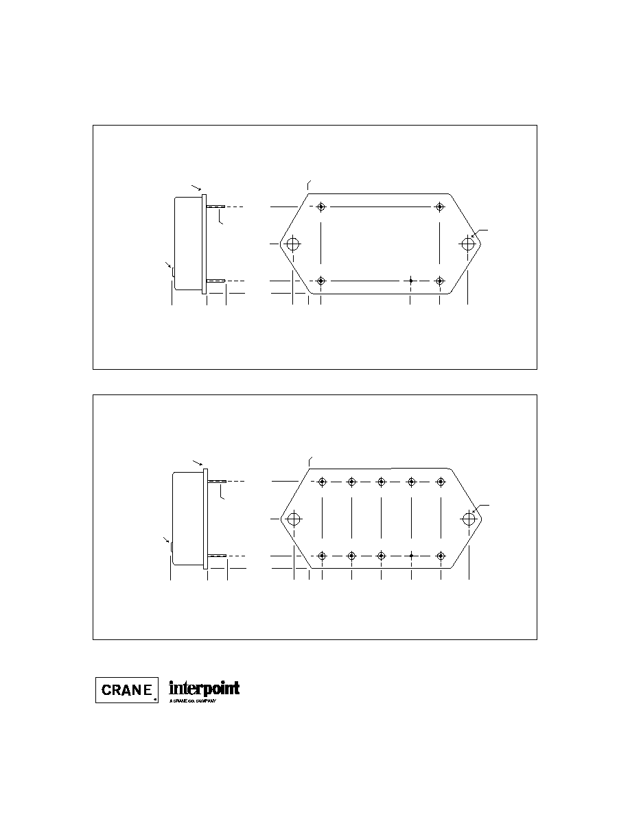
PIN OUT
Pin
Designation
1
Positive Input
2
+5 VDC Output
3
Output Common
4
Negative Aux. Output
5
Positive Aux. Output
6
No Connection
7
Case Ground
8
Inhibit
9
No Connection
10
Input Common
BOTTOM VIEW
MTO
10
9
8
7
6
1
2
3
4
5
Squared corner and dot on
top of cover indicate pin one.
Dotted line outlines flanged package option.
See Section B8, Cases F4 and J5, for dimensions
F
IGURE
3: P
IN
O
UT
MTO 12 12 T F / ES
Base Model
Input Voltage
Output Voltage
Number of Outputs
(T = triple)
(Aux. Vout)
Screening
Case Option
(Non-flanged case has no designator in
this position)
(Standard screening has no designator
in this position.)
MODEL NUMBERING KEY
24223-001-DTS Rev A
DQ# 1021
All technical information is believed to be accurate, but no responsibility is
assumed for errors or omissions. Interpoint reserves the right to make changes in
products or specifications without notice. MTO Series is a trademark of Interpoint.
Copyright © 1990 - 1999 Interpoint. All rights reserved.
B8-12
CASE F
C
ASES
Materials
Header Case F1
Cold Rolled Steel/Nickel/Gold
Cases F2 - F4
Cold Rolled Steel/Nickel/Tin
Cover Case
F1
Kovar/Nickel
Cases F2 - F4
Cold Rolled Steel/Nickel/Tin
Pins
#52 alloy (all cases)
MHV Series Triple ≠ compression glass seal
MTR Series Triple, case F1 ≠ ceramic seal
MTR Series Triple, case F2 ≠ compression glass seal
HUM40 ≠ compression glass seal or ceramic seal
Case F3 ≠ compression glass seal
Case F4 ≠ compression glass seal or ceramic seal
Case dimensions in inches (mm)
Tolerance
±
0.005 (0.13) for three decimal places
±
0.01 (0.2) for two decimal places
unless otherwise specified
CASE F
BOTTOM VIEW
See Figures 20 - 23 for pin configuration
1.350 max
(34.29)
1.950 max
(49.53)
CAUTION
Heat from reflow or wave soldering may damage
the device. Solder pins individually with heat
application not exceeding 300
∞
C for 10 seconds
per pin.
Dot on top of case indicates pin one
10
9
8
7
6
0.000
0.170
(4.32)
1.170
(29.72)
0.000
0.170
(4.32)
0.570
(14.48)
0.970
(24.64)
1.370
(34.80)
1.770
(44.96)
1
2
3
4
5
0.040 dia.
(1.02)
0.000
0.25 (6.4)
MTR
Series
MHV
Series
0.405 max
(10.29)
0.000
0.405 max
(10.29)
Bathtub
Platform
MTR Series Triple and MHV Series Triple: Screening ≠ Standard, ES, or 883
BOTTOM VIEW CASE F1
Seam Seal
0.25 (6.4)
Dot on top of case indicates pin one
F
IGURE
20: C
ASE
F1
F
IGURE
19: C
ASE
F M
AXIMUM
D
IMENSIONS
Note: Although every effort has been made to render the case drawings at actual size, variations in the printing process may cause some distortion. Please refer
to the numerical dimensions for accuracy.

B8-14
CASE F
C
ASES
0.000
0.170
(4.32)
1.170
(29.72)
0.000
0.170
(4.32)
0.570
(14.48)
0.970
(24.64)
1.370
(34.80)
1.770
(44.96)
0.040 dia.
(1.02)
0.000
MTO and MHL Series: Screening ≠ Standard or ES
HR153 Series: no screening options
BOTTOM VIEW CASE F4
0.250/0.300
(6.35/7.62)
Solder Seal
0.505 max
(12.83)
Solder Tip-off
10
9
8
7
6
1
2
3
4
5
Squared corner and dot on top
of case indicate pin one.
F
IGURE
23: C
ASE
F4

B8-22
CASE J
C
ASES
Materials
Header Case J1
Cold Rolled Steel/Nickel/Gold
Cases J2 - J5
Cold Rolled Steel/Nickel/Tin
Cover Case
J1
Kovar/Nickel
Case J2 - J5
Cold Rolled Steel/Nickel/Tin
Pins
#52 alloy (all cases)
Case J1
MHV Series Triple ≠ compression glass seal
MTR Series Triple ≠ ceramic seal
Cases J2 - J5
compression glass seal
Case dimensions in inches (mm)
Tolerance
±
0.005 (0.13) for three decimal places
±
0.01 (0.2) for two decimal places
unless otherwise specified
CASE J
BOTTOM VIEW
See Figures 36 - 40
for pin configuration
1.350 max
(34.29)
CAUTION
Heat from reflow or wave soldering may damage
the device. Solder pins individually with heat
application not exceeding 300
∞
C for 10 seconds
per pin.
Flange Thickness:
Cases J1 and J5
0.060 (1.52)
Case J2
0.073 (1.85) max
Cases J3 and J4
0.067 +0.005/-0.007 (1.70 +0.13/-0.8)
2.720 max
(69.09)
Dot on top of case indicates pin one
F
IGURE
35: C
ASE
J M
AXIMUM
D
IMENSIONS
Note: Although every effort has been made to render the case drawings at actual size, variations in the printing process may cause some distortion. Please refer
to the numerical dimensions for accuracy.
B8-25
CASE J
C
ASES
0.040 dia.
(1.02)
0.000
0.25 (6.4)
5
4
3
0.000
0.170
(4.32)
0.210
(5.33)
1.370
(34.80)
1.770
(44.96)
1.980
(50.29)
1
2
0.173
(4.39)
0.000
1.173
(29.79
0.673
(17.09)
0.162 dia
(4.11)
Flanged cases: Designator required in Case Option position of model number.
FMD28-461 EMI Filter (down-leaded): Screening ≠ Standard or ES
BOTTOM VIEW CASE J4
Solder Seal
Solder Tip-off
0.505 max
(12.83)
Squared corner and dot on top
of case indicate pin one.
F
IGURE
39: C
ASE
J4
0.040 dia.
(1.02)
0.000
0.25 (6.4)
10
9
8
7
6
0.000
0.170
(4.32)
0.210
(5.33)
0.570
(14.48)
0.970
(24.64)
1.370
(34.80)
1.770
(44.96)
1.980
(50.29)
1
2
3
4
5
0.173
(4.39)
0.000
1.173
(29.79
0.673
(17.09)
0.162 dia
(4.11)
Flanged cases: Designator required in Case Option position of model number
for MHL Series and MTO Series only.
MHL Series, MTO Series, MTW Series: Screening ≠ Standard or ES
HR300 Series: no screening options
BOTTOM VIEW CASE J5
Solder Seal
Solder Tip-off
0.505 max
(12.83)
Squared corner and dot on top
of case indicate pin one.
F
IGURE
40: C
ASE
J5

C2-12
QA SCREENING
85∞C PRODUCTS
TEST (85∞C Products excluding HR products)
STANDARD
/ES
PRE-CAP INSPECTION
Method 2017
yes
yes
TEMPERATURE CYCLE (10 times)
Method 1010, Cond. B, -55∞C to 125∞C
no
yes
CONSTANT ACCELERATION
Method 2001, 500 g
no
yes
BURN-IN
96 hours at 70∞C ambient (typical)
no
yes
FINAL ELECTRICAL TEST MIL-PRF-38534, Group A
Subgroups 1 and 4: +25∞C case
yes
yes
HERMETICITY TESTING
Fine Leak, Method 1014, Cond. A
no
yes
Gross Leak, Method 1014, Cond. C
no
yes
Gross Leak, Dip (1 x 10
-3
)
yes
no
FINAL VISUAL INSPECTION
Method 2009
yes
yes
Test methods are referenced to MIL-STD-883 as determined by MIL-PRF-38534.
MFW Series
MTW Series
MHE/MLP Series
MHL Series
MRH Series
MTO Series
MSR Series
DCH Series
FM/FMA/FMB EMI Filters
MSF EMI Filter
85∞C P
RODUCTS
Applies to the following products: