
Engineering Specification
Type 15.0 XGA Color TFT/LCD Module
Model Name:N150X4-L01
Document Control Number : OEM N150X4-L01-01
Note:Specification is subject to change without notice. Consequently it is better to contact to
International Display Technology before proceeding with the design
of your product incorporating this module.
Sales Support
International Display Technology
Engineering Specification
(C) Copyright International Display Technology 2002 All Rights reserved.
February 06,2003
OEM N150X4-L01-01
1/29

i Contents
i Contents
ii Record of Revision
1.0 Handling Precautions
2.0 General Description
2.1 Characteristics
2.2 Functional Block Diagram
3.0 Absolute Maximum Ratings
4.0 Optical Characteristics
5.0 Signal Interface
5.1 Connectors
5.2 Interface Signal Connector
5.3 Interface Signal Description
5.3.1 E-EDUD
5.4 Interface Signal Electrical Characteristics
5.4.1 Signal Electrical Characteristics for LVDS Receiver
5.4.2 LVDS Receiver Internal Circuit
5.4.3 Recommended Guidelines for Motherboard PCB Design and Cable Selection
5.5 Signal for Lamp connector
6.0 Pixel format image
7.0 Parameter guide line for CFL Inverter
8.0 Interface Timings
8.1 Timing Characteristics
8.2 Timing Definition
9.0 Power Consumption
10.0 Power ON/OFF Sequence
11.0 Mechanical Characteristics
12.0 National Test Lab Requirement
Engineering Specification
(C) Copyright International Display Technology 2002 All Rights reserved.
February 06,2003
OEM N150X4-L01-01
2/29
ii Record of Revision
First Edition for customer.
Based on Internal Spec."N150X4-IPI-01"
All
OEM N150X4-L01-01
February 06,2003
Summary
Page
Document Revision
Date
Engineering Specification
(C) Copyright International Display Technology 2002 All Rights reserved.
February 06,2003
OEM N150X4-L01-01
3/29
1.0 Handling Precautions
O
If any signals or power lines deviate from the power on/off sequence, it may cause shorten the life of the
LCD module.
O
The LCD panel and the CFL are made of glass and may break or crack if dropped on a hard surface, so
please handle them with care.
O
CMOS ICs are included in the LCD panel. They should be handled with care, to prevent electrostatic
discharge.
O
Do not press the reflector sheet at the LCD module to any directions.
O
Do not stick the adhesive tape on the reflector sheet at the back of the LCD module.
O
Please handle with care when mount in the system cover. Mechanical damage for lamp cable/lamp
connector may cause safety problems.
O
Small amount of materials having no flammability grade is used in the LCD module. The LCD module
should be supplied by power complied with requirements of Limited Power Source (2.5, IEC60950 or
UL60950), or be applied exemption conditions of flammability requirements (4.7.3.4, IEC60950 or
UL60950) in an end product.
O
The LCD module is designed so that the CFL in it is supplied by Limited Current Circuit (2.4, IEC60950 or
UL60950).
O
The fluorescent lamp in the liquid crystal display(LCD) contains mercury. Do not put it in trash that is
disposed of in landfills. Dispose of it as required by local ordinances or regulations.
O
Never apply detergent or other liquid directly to the screen.
O
Wipe off water drop immediately. Long contact with water may cause discoloration or spots.
O
When the panel surface is soiled, wipe it with absorbent cotton or other soft cloth; do not use solvents or
abrasives.
O
Do not touch the front screen surface in your system, even bezel.
O
Gently wipe the covers and the screen with a soft cloth.
The information contained herein may be changed without prior notice. It is therefore
advisable to contact International Display Technology before proceeding with the design of
equipment incorporating this product.
O
The information contained herein is presented only as a guide for the applications of our
products. No responsibility is assumed by International Display Technology for any
infringements of patents or other right of the third partied which may result from its use. No
license is granted by implication or otherwise under any patent or patent rights of International
Display Technology or others.
O
Engineering Specification
(C) Copyright International Display Technology 2002 All Rights reserved.
February 06,2003
OEM N150X4-L01-01
4/29

2.0 General Description
This specification applies to the Type 15.0 Color TFT/LCD Module 'N150X4-L01'.
This module is designed for a display unit of a notebook style personal computer.
The screen format and electrical interface are intended to support the XGA (1024(H) x 768(V)) screen.
Support color is native 262k colors ( RGB 6-bit data driver ).
All input signals are LVDS(Low Voltage Differential Signaling) interface compatible.
This module does not contain an inverter card for backlight.
Engineering Specification
(C) Copyright International Display Technology 2002 All Rights reserved.
February 06,2003
OEM N150X4-L01-01
5/29
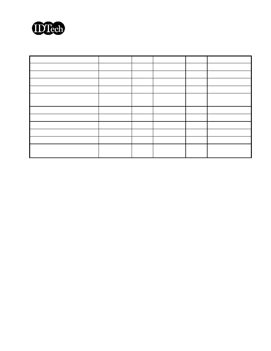
2.1 Characteristics
The following items are characteristics summary on the table under 25 degree C condition:
60 mm
CFL cable length
0 to +50 (Operating)
-20 to +60 (Storage, Shipping)
Temperature Range [deg. C]
Native 262K colors ( RGB 6-bit data driver )
Support Color
4 pairs Single LVDS(Single)
Electrical Interface
317.3(W) x 242.0(H) x 6.2(D) Typ.
Physical Size [mm]
585 Max.
Weight [grams]
4.1Typ.(@ICFL=6.5mA)
CFL Power Consumption [watt]
1.6 Typ. (All White Pattern), 2.2 Max (worst pattern)
Logic Power Consumption [watt]
+3.3 V
Nominal Input Voltage [VDD]
60msec Typ.; 120ms Max. (@25degC)
Optical Rise + Fall Time
Anti-Glare,AG160
Surface Treatment
x:0.313 , y:0.329
Color Chromaticity
CR>=10:1 H: +/-85 deg., V:+/-85 deg. Typ.
CR>=100:1 H: +/-40 deg., V:+/-40 deg. Typ.
Viewing Angle
400 : 1 Typ. 300:1 Min
Contrast Ratio
215 Typ. (Screen Center, ICFL = 6.5mA)
White Luminance [cd/m
2
]
Normally Black
Display Mode
R.G.B. Vertical Stripe
Pixel Arrangement
0.297(per one triad) x 0.297
Pixel Pitch [mm]
1024(x3) x 768
Pixels H x V [pixels]
304.128(H) x 228.096(V)
Active Area [mm]
38
Screen Diagonal [cm]
SPECIFICATIONS
CHARACTERISTICS ITEMS
Engineering Specification
(C) Copyright International Display Technology 2002 All Rights reserved.
February 06,2003
OEM N150X4-L01-01
6/29
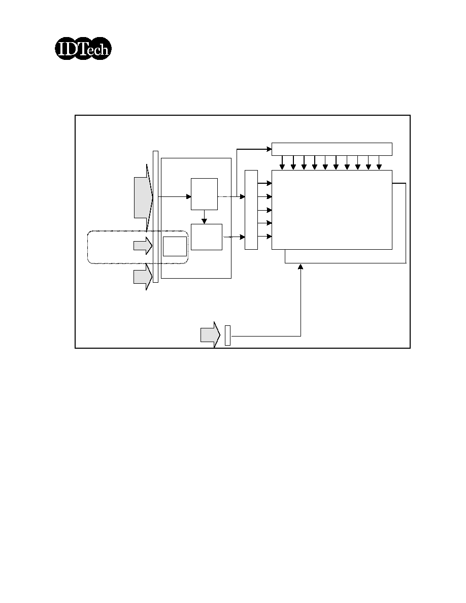
2.2 Functional Block Diagram
The following diagram shows the functional block of the Type 15.0 Color TFT/LCD Module.
TFT ARRAY/CELL
VDD
LCD
Controller
LCD DRIVE
CARD
Backlight Unit
1024(R/G/B) x 768
GND
DC-DC
Converter
Ref circuit
Y-Driver
X-Driver
<4 pairs LVDS>
RxIN1
RxIN0
RxIN2
RxCLKIN
FI-XB30SL-HF10
BHSR-02VS-1 (JST)
CCFL High Voltate
CCFL Low Voltage
Signal Connector
CCFL Connector
VDD
VDD
VDD
EEDID
Chip
VEEDID
CLCEEDID
DataEEDID
Engineering Specification
(C) Copyright International Display Technology 2002 All Rights reserved.
February 06,2003
OEM N150X4-L01-01
7/29
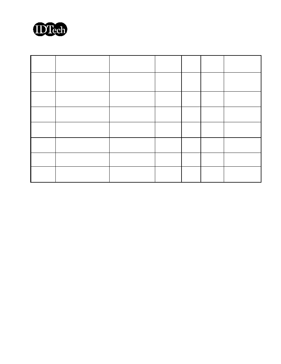
3.0 Absolute Maximum Ratings
Absolute maximum ratings of the module is as follows :
Rectangle wave
G ms
50 18
Shock
G Hz
1.5 10-200
Vibration
(Note 1)
%RH
95
5
HST
Storage Relative Humidity
(Note 1)
deg.C
+60
-20
TST
Storage Temperature
(Note 1)
%RH
95
8
HOP
Operating Relative Humidity
(Note 1)
deg.C
+50
0
TOP
Operating Temperature
A single pulse
20mA / 50ms
-
ICFLP
CFL Peak Inrush Current
mArms
7
-
ICFL
CFL Current
Vrms
2,000
-
Vinv
Lamp Ignition Voltage
V
VDD+0.3
-0.3
Other Inputs
Input Voltage of Signal
V
+4.0
-0.3
VDD
Supply Voltage
Conditions
Unit
Max
Min
Symbol
Item
Note :
1.
Maximum Wet-Bulb should be 39 degree C and No condensation.
Engineering Specification
(C) Copyright International Display Technology 2002 All Rights reserved.
February 06,2003
OEM N150X4-L01-01
8/29

4.0 Optical Characteristics
The optical characteristics are measured under stable conditions as follows under 25 degree C condition:
160Min
Center
200Typ.
Center
White Luminance (cd/m
2
)
ICFL 6.0 mA
-
0.329
White y
-
0.313
White x
-
-
Blue y
-
-
Blue x
-
-
Green y
-
-
Green x
(CIE)
-
-
Red y
Chromaticity
-
-
Red x
Color
(ms)
120 Max.
60
Rising + Falling
Response Time
-
400
Contrast ratio
-
-
85
85
Vertical (Upper)
K
P
10 (Lower)
K:Contrast Ratio
-
-
85
85
Horizontal (Right)
K
P
10 (Left)
Viewing Angle
(Degrees)
Note
Typ.
Specification
Conditions
Item
Engineering Specification
(C) Copyright International Display Technology 2002 All Rights reserved.
February 06,2003
OEM N150X4-L01-01
9/29
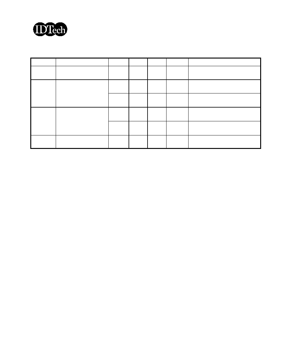
5.0 Signal Interface
5.1 Connectors
Physical interface is described as for the connector on module.
These connectors are capable of accommodating the following signals and will be following components.
FI-X30M, FI-X30C2L
Mating Receptacle/Part Number
FI-XB30SL-HF10
Type / Part Number
JAE
Manufacturer
For Signal Connector
Connector Name / Designation
SM02B-BHSS-1
Mating Type / Part Number
BHSR-02VS-1
Type / Part Number
JST
Manufacturer
For Lamp Connector
Connector Name / Designation
Engineering Specification
(C) Copyright International Display Technology 2002 All Rights reserved.
February 06,2003
OEM N150X4-L01-01
10/29
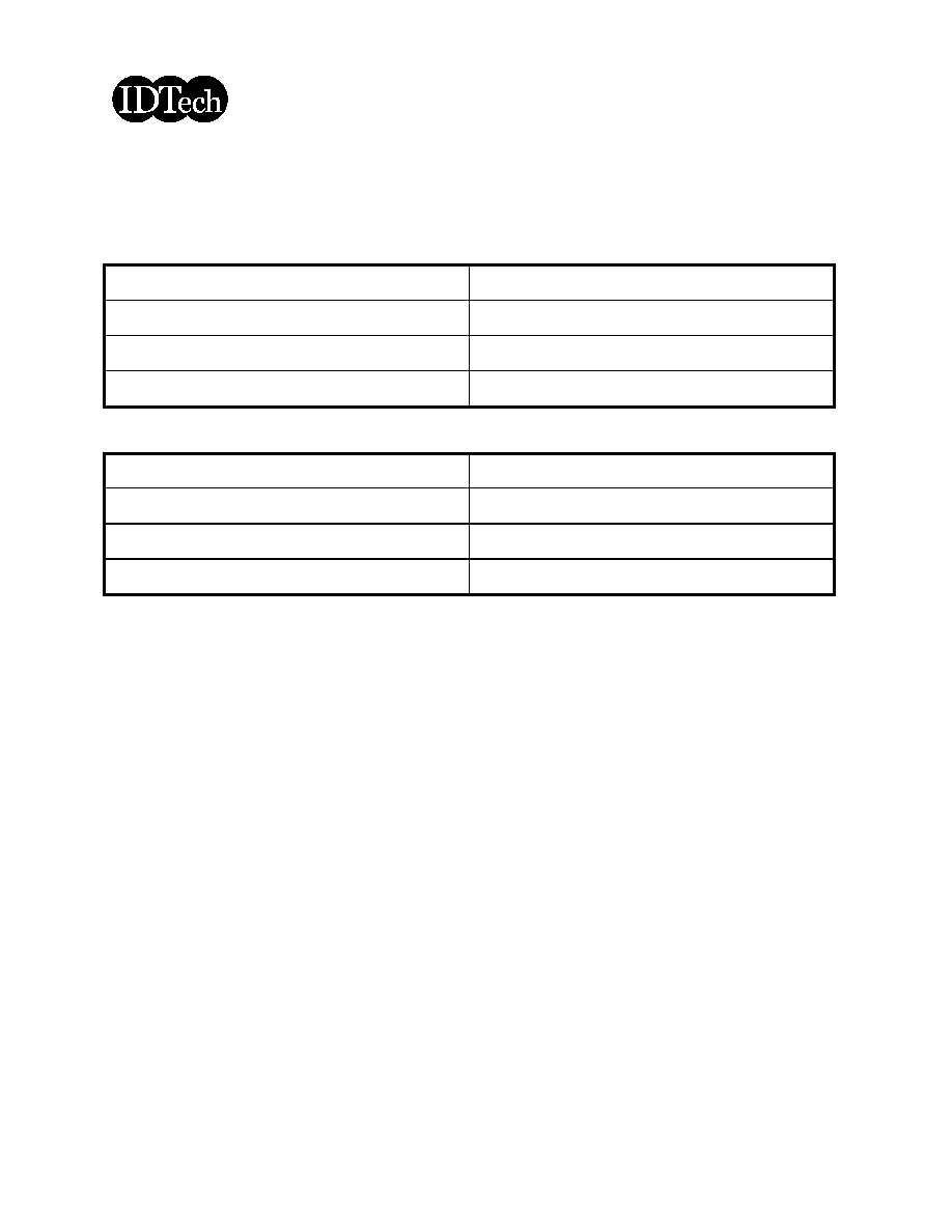
5.2 Interface Signal Connector
NC
30
RxIN2+
15
NC
29
RxIN2-
14
GND
28
GND
13
NC
27
RxIN1+
12
NC
26
RxIN1-
11
GND
25
GND
10
NC
24
RxIN0+
9
NC
23
RxIN0-
8
GND
22
Data
EEDID
(Note 2, 4)
7
NC
21
CLK
EEDID
(Note 2, 4)
6
NC
20
Reserved (Note 1)
5
GND
19
V
EDID
(Note 2, 3)
4
RxCLKIN+
18
VDD
3
RxCLKIN-
17
VDD
2
GND
16
GND
1
Signal Name
Pin #
Signal Name
Pin #
Note :
1.
'Reserved' pins are not allowed to connect any other line.
2.
This LCD Module complies with "VESA ENHANCED EXTENDED DISPLAY IDENTIFICATION DATA
STANDARD Release A, Revision 1" and supports "EEDID version 1.3".
3.
V
EEDID
power source shall be the limited current circuit which has not exceeding 1A. (Reference Document :
"Enhanced Display Data Channel (E-DDC
TM
) Proposed Standard", VESA)
4.
Both CLK
EEDID
line and DATA
EEDID
line are pulled up with 10k ohm resistor to V
EEDID
power source line at LCD
panel, respectively.
Voltage levels of all input signals are LVDS compatible (except VDD, EEDID). Refer to "Signal Electrical
Characteristics for LVDS Receiver", for voltage levels of all input signals.
5.3 Interface Signal Description
Signal Description
Ground
GND
+3.3V Power Supply
VDD
LVDS differential clock input
RxCLKIN+, RxCLKIN-
LVDS differential data input (Blue2-Blue5, HSync, VSync, DSPTMG)
RxIN2+, RxIN2-
LVDS differential data input (Green1-Green5,Blue0-Blue1)
RxIN1+, RxIN1-
LVDS differential data input (Red0-Red5, Green0)
RxIN0+, RxIN0-
Description
Signal Name
Note :
O
Input signals shall be low or Hi-Z state when VDD is off.
Engineering Specification
(C) Copyright International Display Technology 2002 All Rights reserved.
February 06,2003
OEM N150X4-L01-01
11/29
EEDID Data
Data
EEDID
EEDID Clock
CLK
EDID
EEDID 3.3 V Power Supply
V
EEDID
Ground
GND
Power Supply
VDD
Horizontal Sync:The signal is synchronized with DTCLK . Both active high/low
signals are acceptable.
HSYNC(H-S)
Vertical Sync:The signal is synchronized to DTCLK . Both active high/low
signal acceptable.
VSYNC(V-S)
When the signal is high, the pixel data shall be valid to be displayed.
+DSPTMG(DSP)
Data Clock:The typical frequency is 65.0 MHz.
The signal is used to strobe the pixel data and the DSPTMG .
DTCLK
Blue Data 5 (MSB)
Blue Data 4
Blue Data 3
Blue Data 2
Blue Data 1
Blue Data 0 (LSB)
Blue-pixel Data: Each blue pixel's brightness data consists of these 6 bits pixel data.
+BLUE 5
+BLUE 4
+BLUE 3
+BLUE 2
+BLUE 1
+BLUE 0
Green Data 5 (MSB)
Green Data 4
Green Data 3
Green Data 2
Green Data 1
Green Data 0 (LSB)
Green-pixel Data: Each green pixel's brightness data consists of these 6 bits pixel data.
+GREEN 5
+GREEN 4
+GREEN 3
+GREEN 2
+GREEN 1
+GREEN 0
Red Data 5 (MSB)
Red Data 4
Red Data 3
Red Data 2
Red Data 1
Red Data 0 (LSB)
Red-pixel Data: Each red pixcel's brightness data consists of these 6 bits pixel data.
+RED5
+RED4
+RED3
+RED2
+RED1
+RED0
Description
SIGNAL NAME
Note : Output signals except V
EEDID
, CLK
EEDID
and Data
EEDID
from any system shall be Hi-Z state when VDD is
off.
Engineering Specification
(C) Copyright International Display Technology 2002 All Rights reserved.
February 06,2003
OEM N150X4-L01-01
12/29
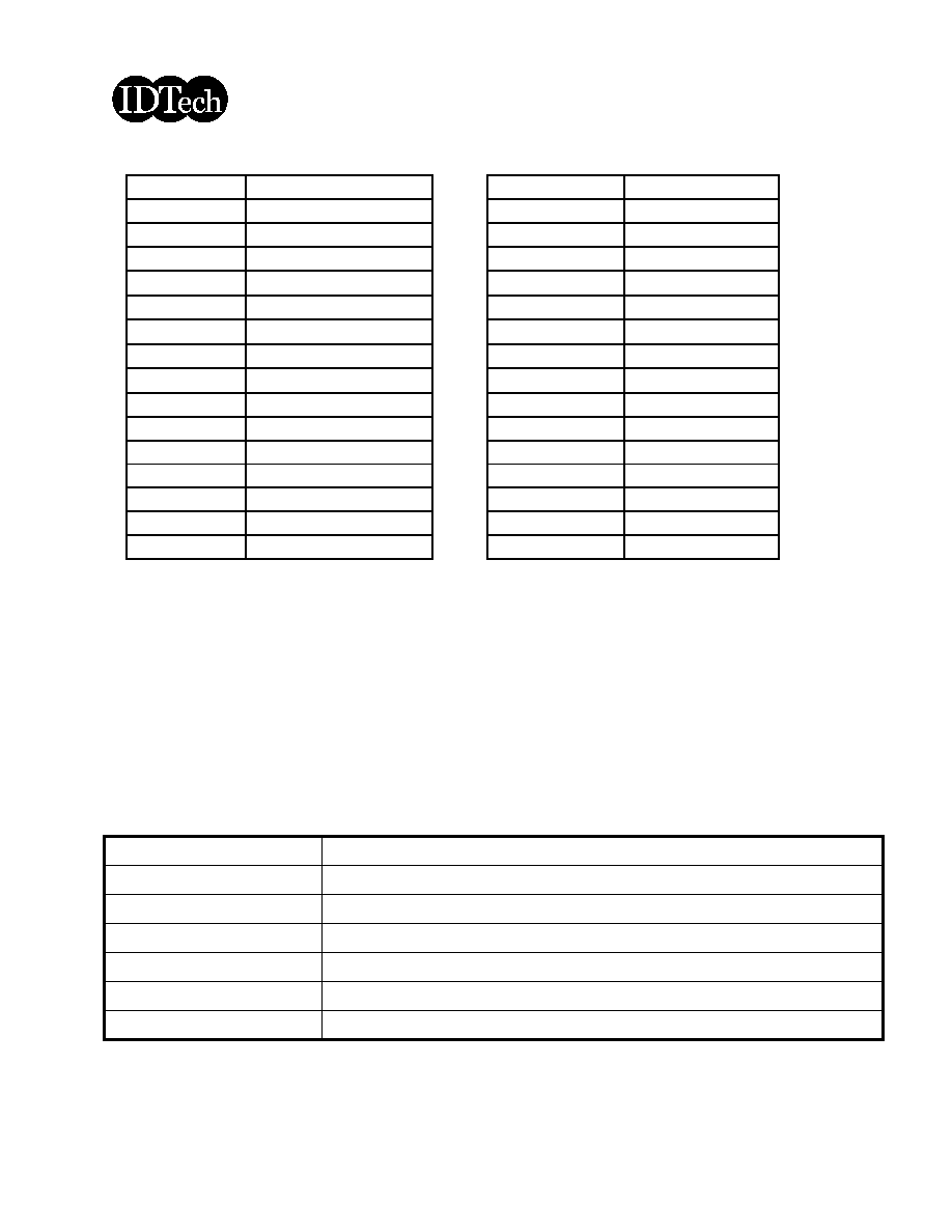
5.3.1
E-EDID
E-EDID detail in this LCD module is in the following table.
(Note 1)
Checksum
7F
No extension
00
Extension Flag
7E
Manufacturer P/N
"N150X4"
00 00 00 FE 00 4E 31
35 30 58 34 0A 20 20
20 20 20 20
Detailed Timing /
Monitor Description #4
6C - 7D
Manufactuerer name
"IDT"
00 00 00 FE 00 49 44
54 0A 20 20 20 20 20
20 20 20 20
Detailed Timing /
Monitor Description #3
5A - 6B
(Note 1)
Detailed Timing /
Monitor Description #2
48 - 59
Typical Timing
64 19 00 40 41 00 26
30 18 88 36 00 30 E4
10 00 00 18
Detailed Timing /
Monitor Description #1
36 - 47
Unused
01 01 01 01 01 01 01
01 01 01 01 01 01 01
01 01
Standard Timing
Identification
26 - 35
Unused
00 00 00
Established Timing
23 - 25
(Note 1)
Color Characteristics
19 - 22
Active Area : 30.41cm x
22.81cm,
Gamma : 2.2
80 1E 17 78 0A
Basic Display
Parameter / Features
14 - 18
Ver1.3
01 03
EDID Structure Version
/ Revision
12 - 13
Unused
00
Year of Manufacture
11
Unused
00
Week of Manufacture
10
Unused
00 00 00 00
ID Serial Number
0C - 0F
Product Code
0D 00
ID Product Code
0A - 0B
"IDT"
24 94
ID Manufacturer Name
08 - 09
Header, Fixed
00 FF FF FF FF FF FF
00
Header
00 - 07
Remark
Data (hex)
Description
Address
(hex)
Note:
1.Detail data contents shall be determined with concurrence between user and International Display Technology(IDTech).
Engineering Specification
(C) Copyright International Display Technology 2002 All Rights reserved.
February 06,2003
OEM N150X4-L01-01
13/29
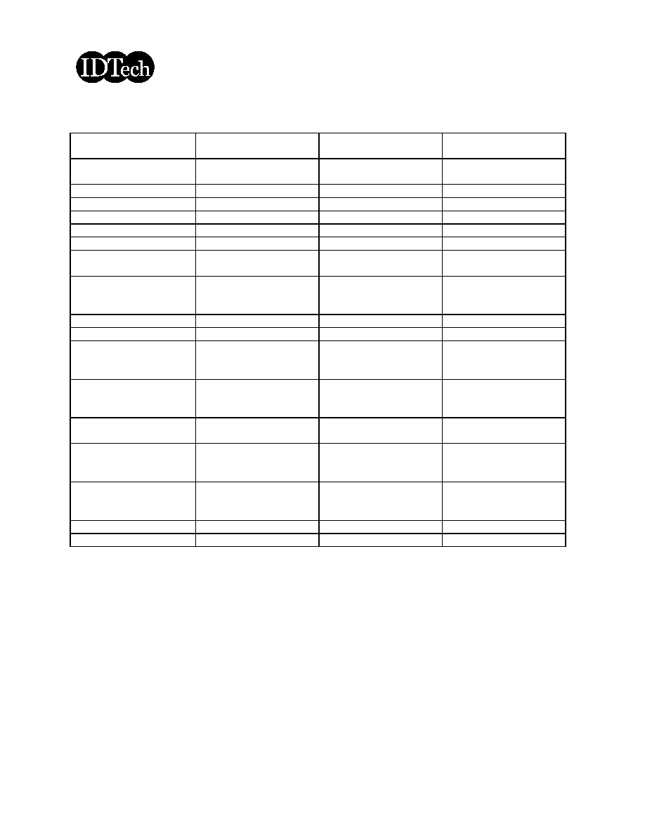
5.4 Interface Signal Electrical Characteristics
5.4.1 Signal Electrical Characteristics for LVDS Receiver
The LVDS receiver equipped in this LCD module is compatible with ANSI/TIA/TIA-644 standard.
Electrical Characteristics
Vth - Vtl = 200mV
mV
+50
-50
Vcm
Common Mode Voltage Offset
Vth - Vtl = 200mV
V
1.5
1.2
1.0
Vcm
Common Mode Voltage
mV
600
100
|Vid|
Magnitude Differential Input Voltage
Vcm=+1.2V
mV
-100
Vtl
Differential Input Low Threshold
Vcm=+1.2V
mV
+100
Vth
Differential Input High Threshold
Conditions
Unit
Max
Typ
Min
Symbol
Parameter
Note :
O
Input signals shall be low or Hi-Z state when VDD is off.
Voltage Definitions
Engineering Specification
(C) Copyright International Display Technology 2002 All Rights reserved.
February 06,2003
OEM N150X4-L01-01
14/29
Measurement System
Timming Requirements
fc = 65MHz, Tsu=Thd=900ps
ps/clk
20
tCJavg
Cycle Modulation Rate (Note 4)
fc = 65MHz, Tsu=Thd=900ps
ps
+150
-150
tCCJ
Cycle-to-cycle jitter (Note 3)
ps
500
Thd
Data Hold Time (Note 2)
fc = 65MHz, tCCJ < 50ps,
Vth-Vtl = 400mV,
Vcm = 1.2V,
Vcm = 0
ps
500
Tsu
Data Setup Time (Note 1)
ns
20.00
15.38
14.93
tc
Cycle Time
MHz
67
65
50
fc
Clock Frequency
Conditions
Unit
Max
Typ
Min
Symbol
Parameter
Note :
1.
All values are at VDD=3.3V, Ta=25 degree C.
2.
See figure "Timing Definition" and "Timing Definition(detail A)" for definition.
3.
Jitter is the magnitude of the change in input clock period.
4.
This specification defines maximum average cycle modulation rate in peak-to-peak transition within any 100
clock cycles. Figure "Cycle Modulation Rate" illustrates a case against this requirement.
This specification is applied only if input clock peak jitter within any 100 clock cycles is greater than 300ps.
Engineering Specification
(C) Copyright International Display Technology 2002 All Rights reserved.
February 06,2003
OEM N150X4-L01-01
15/29
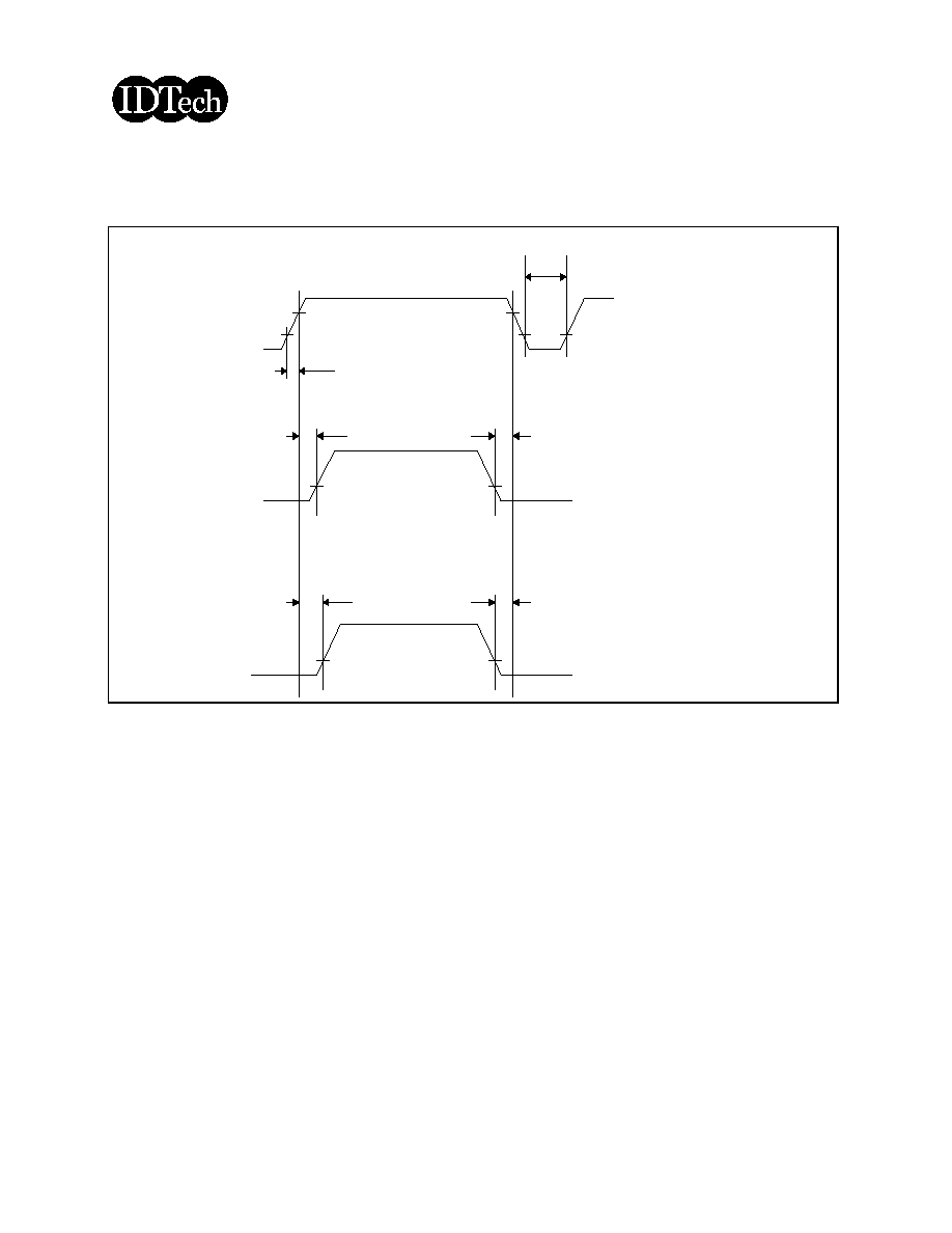
Timing Definition
Engineering Specification
(C) Copyright International Display Technology 2002 All Rights reserved.
February 06,2003
OEM N150X4-L01-01
16/29
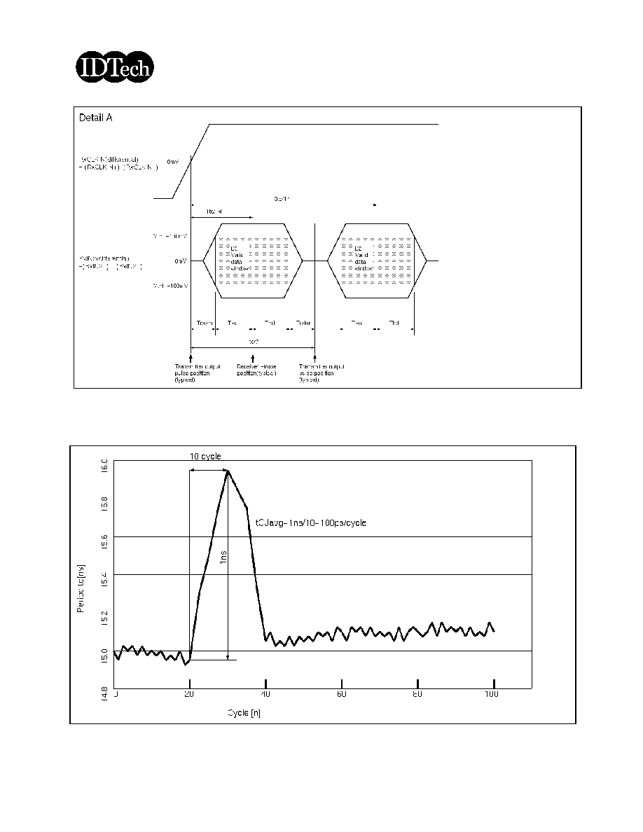
Timing Definition(detail A)
Note: Tsu and Thd are internal data sampling window of receiver. Trskm is the system skew margin; i.e., the sum
of cable skew, source clock jitter, and other inter-symbol interference, shall be less than Trskm.
Cycle Modulation Rate
Engineering Specification
(C) Copyright International Display Technology 2002 All Rights reserved.
February 06,2003
OEM N150X4-L01-01
17/29
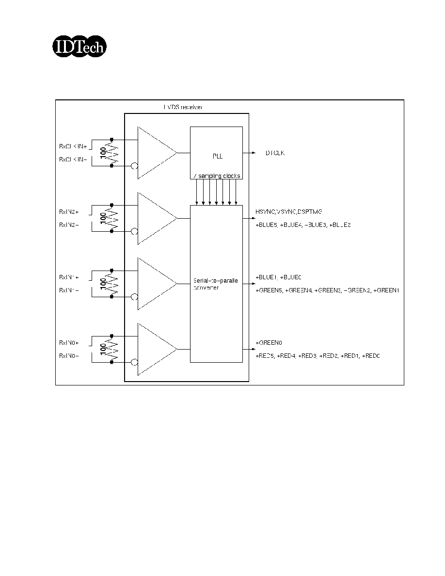
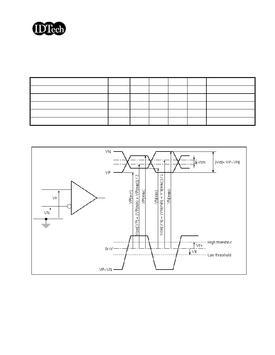
5.4.2 LVDS Receiver Internal Circuit
The following figure shows the internal block diagram of the LVDS receiver. This LCD module equips termination
resistors for LVDS link.
5.4.3 Recommended Guidelines for Motherboard PCB Design and Cable Selection
Following the suggestions below will help to achieve optimal results.
O
Use controlled impedance media for LVDS signals. They should have a matched differential
impedance of 100 ohm.
O
Match electrical lengths between traces to minimize signal skew.
O
Isolate TTL signals from LVDS signals.
O
For cables, twisted pair, twin, or flex circuit with close coupled differential traces are recommended.
Engineering Specification
(C) Copyright International Display Technology 2002 All Rights reserved.
February 06,2003
OEM N150X4-L01-01
18/29
5.5 Signal for Lamp Connector
Lamp Low Voltage
2
Lamp High Voltage
1
Signal Name
Pin #
Engineering Specification
(C) Copyright International Display Technology 2002 All Rights reserved.
February 06,2003
OEM N150X4-L01-01
19/29
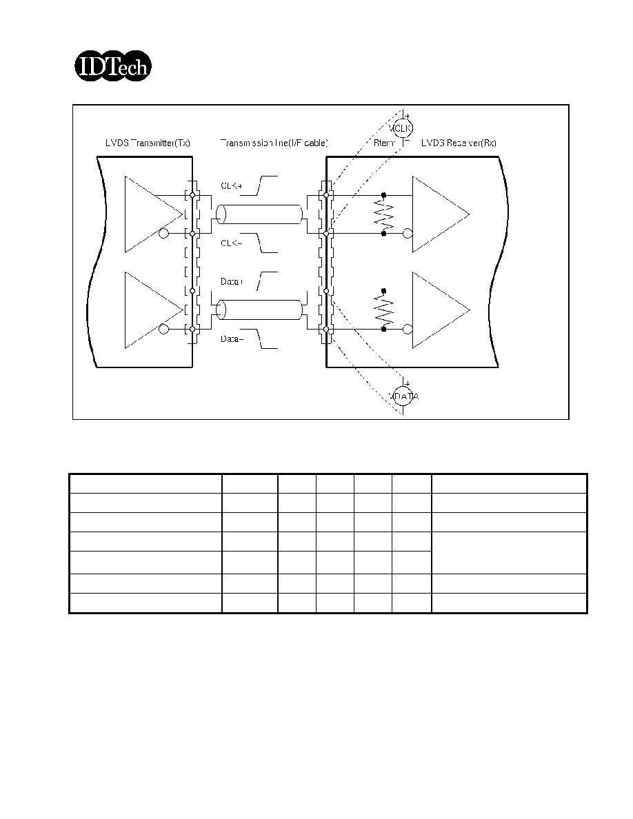
6.0 Pixel format image
Following figure shows the relationship of the input signals and LCD pixel format image. Even and odd pair of
RGB data are sampled at a time
.
0
R
1
1022 1023
1st Line
768th Line
GB
RG
RG B
B R G B
RG B R G B
RG B RG B
Engineering Specification
(C) Copyright International Display Technology 2002 All Rights reserved.
February 06,2003
OEM N150X4-L01-01
20/29
7.0 Parameter guide line for CFL Inverter
Ta=25[deg. C]
(Note 4)
[W]
4.1
CFL Power
consumption
PCFL
Ta=25[deg. C]
[Vrms]
630
CFL Voltage
(Reference)
VCFL
Ta=0[deg. C]
[Vrms]
1,600
Inverter Ignition Voltage
VCFLi
Ta=25[deg. C]
(Note 3)
[kHz]
70
40
CFL Frequency
FCFL
Ta=25[deg. C]
(Note 2,6)
[mA]
20
CFL Peak Inrush
Current
ICFLP
Ta=25[deg. C]
(Note 2,5)
[mArms]
7.0
6.5
3.0
CFL current
ICFL
Ta=25[deg. C]
[cd/m
2
]
-
-
215
-
-
White Luminance
(Center)
(L63)
CONDITION
UNITS
MAX
D.P
(Note 1)
MIN
PARAMETER
SYMBOL
Note :
1.
Design Point
2.
If it exceeds MIN/MAX values, then"CFL Life" , "ON/OFF Cycle", and "SAFETY" will not be guaranteed.
3.
CFL Frequency should be carefully determined to avoid interference between inverter and TFT LCD.
4.
Calculated value for reference (ICFL x VCFL = PCFL).
5.
It should be employed the inverter which has `Duty Dimming`, if ICFL is less than 4[mA].
6.
Duration: 50msec MAX
Engineering Specification
(C) Copyright International Display Technology 2002 All Rights reserved.
February 06,2003
OEM N150X4-L01-01
21/29

The following chart is Luminance versus Lamp Current for your reference.
Engineering Specification
(C) Copyright International Display Technology 2002 All Rights reserved.
February 06,2003
OEM N150X4-L01-01
22/29

8.0 Interface Timings
Basically, interface timings should match the VESA 1024x768 / 60 Hz (VG901101) manufacturing guide line
timing. These timings described here are not actual input timings of LCD module but output timings of
SN75LVDS86DGG(Texas Instruments) or equivalent.
8.1 Timing Characteristics
1
tx
63
29
7
V-sync back porch
Vbp
tx
3
1
V-sync front porch
Vfp
tx
6
1
V-sync Width
Vw
Hz
61
60
55
Frame rate
Vsync
tx
768
768
768
Y active time
tacy
tx
1023
806
777
Y total time
ty
tck
24
0
H front porch
Hfp
2
tck
510
160
8
H back porch
Hbp
2
tck
136
8
H-Sync width
Hsw
KHz
48.363
H frequency
Hsync
tck
1024
1024
1024
X active time
tacx
tck
2047
1344
1206
X total time
tx
nsec
20.00
15.38
14.93
DTCLK cycle time
tck
MHz
67.00
65.00
50.00
DTCLK Frequency
fdck
Note
Unit
MAX
TYP
MIN
Symbol
Note1 : Vbp should be static.
Note2 : Hsw+Hbp> 32 [tck]
- The timing interval between V-Sync falling edge and H-Sync rising edge should be fixed between each
V-Frame.(V-Sync and H-Sync polarity are assumed to be positive in this case.)
Engineering Specification
(C) Copyright International Display Technology 2002 All Rights reserved.
February 06,2003
OEM N150X4-L01-01
23/29

8.2 Timing Definition
1344 dot
136 dot
160 dot
24 dot
1024 dot
H-Sync
DSPTMG
38H
3H
29H
6H
768H
V-Sync
DSPTMG
Engineering Specification
(C) Copyright International Display Technology 2002 All Rights reserved.
February 06,2003
OEM N150X4-L01-01
24/29
9.0 Power Consumption
Input power specifications are as follows;
[mVp-p]
100
Allowable Logic/LCD
Drive Ripple Voltage
VDDrp
Max Pattern,
VDD=3.0[V]
[mA]
640
(TBD)
All Black Pattern,
VDD=3.3[V]
[mA]
490
(TBD)
VDD Current
IDD
Max. Pattern,
VDD=3.6[V]
[W]
2.2
(TBD)
All Black Pattern
VDD=3.3[V]
[W]
1.6
(TBD)
VDD Power
PDD
Load Capacitance 20[uF]
[V]
3.6
3.3
3.0
Logic/LCD Drive
Voltage
VDD
CONDITION
UNITS
Max
Typ
Min
PARAMETER
SYMBOL
Engineering Specification
(C) Copyright International Display Technology 2002 All Rights reserved.
February 06,2003
OEM N150X4-L01-01
25/29
10.0 Power ON/OFF Sequence
VDD power and lamp on/off sequence is as follows. Interface signals are also shown in the chart. Signals from
any system shall be Hi-Z state or low level when VDD is off.
90%
10%
10%
10%
90%
0.1ms min.
0 min.
0 min.
0 V
0 V
VDD
Signals
10%
10%
200ms min.
0 min.
0 V
Lamp On
10%
10%
30ms max.
30ms min.
Engineering Specification
(C) Copyright International Display Technology 2002 All Rights reserved.
February 06,2003
OEM N150X4-L01-01
26/29
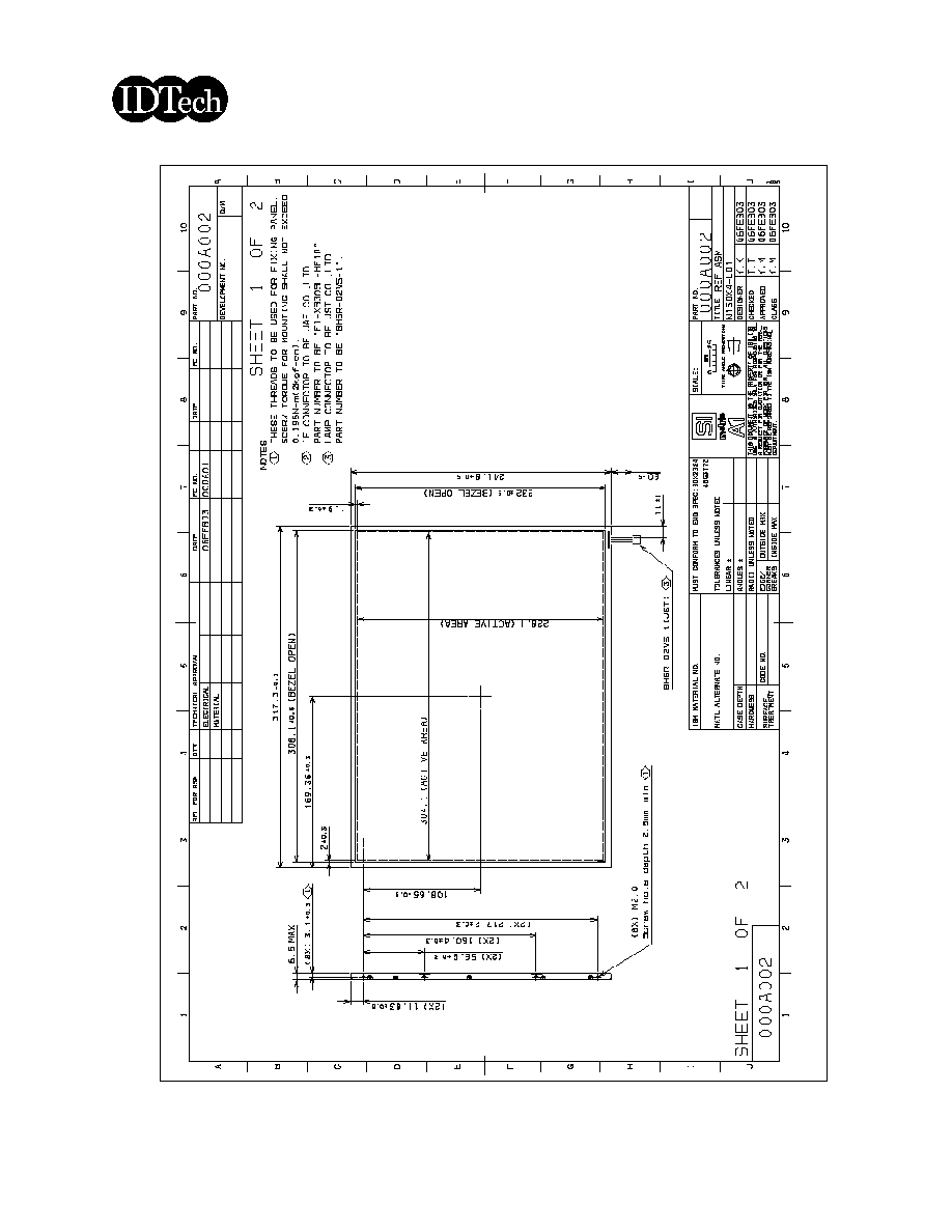
11.0 Mechanical Characteristics
Engineering Specification
(C) Copyright International Display Technology 2002 All Rights reserved.
February 06,2003
OEM N150X4-L01-01
27/29
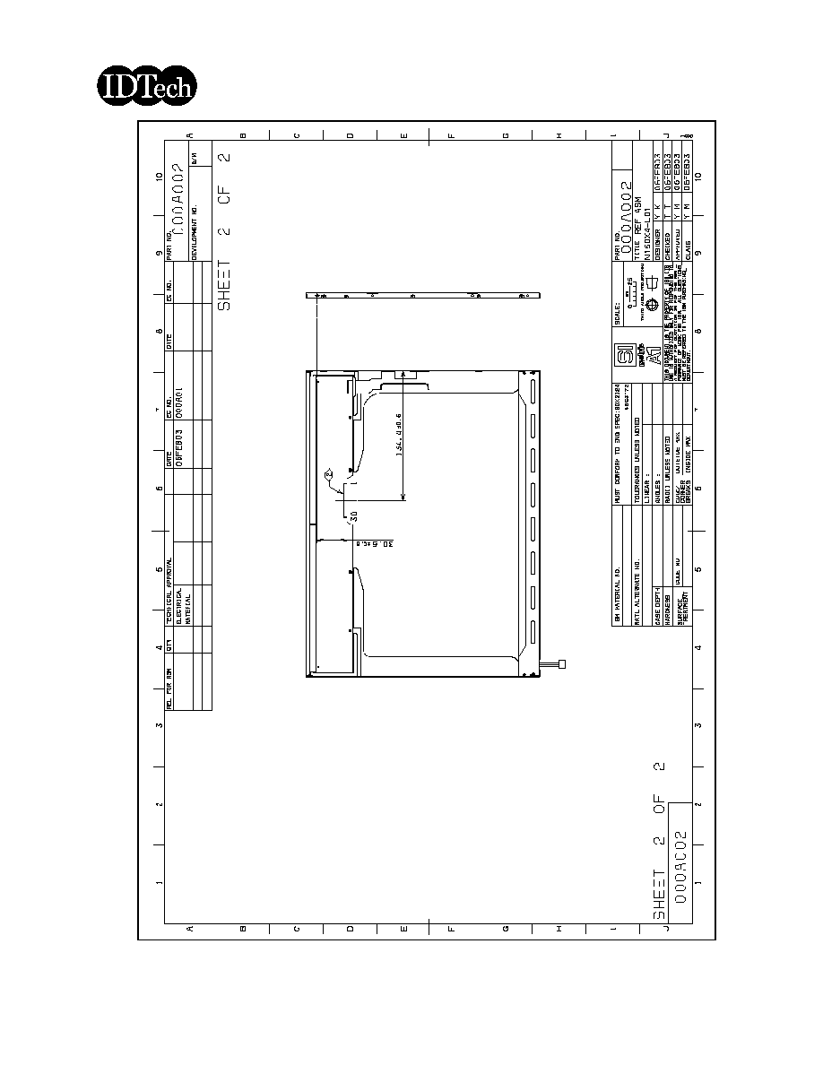
Engineering Specification
(C) Copyright International Display Technology 2002 All Rights reserved.
February 06,2003
OEM N150X4-L01-01
28/29

12.0 National Test Lab Requirement
The display module will satisfy all requirements for compliance to
UL 60950, 3rd Edition U.S.A. Information Technology Equipment
CAN/CSA-C22.2 No. 60950-00 Canada, Information Technology Equipment
IEC 60950 (3rd. Ed.) International, Information Technology Equipment
EN 60950 (3rd. Ed.) International, Information Technology Equipment
(European Norm for IEC60950)
****** End Of Page ******
Engineering Specification
(C) Copyright International Display Technology 2002 All Rights reserved.
February 06,2003
OEM N150X4-L01-01
29/29