1
File Number
3977.2
HS-0508RH, HS-0509RH
Radiation Hardened Single 8/Differential
4-Channel CMOS Analog Multiplexers
These radiation hardened monolithic CMOS multiplexers
each include an array of eight analog switches, a digital
decode circuit for channel selection, a voltage reference for
logic thresholds, and an ENABLE input for device selection
when several multiplexers are present.
The Dielectric Isolation (DI) process used in fabrication of
these devices eliminates the problem of latch-up. Also, DI
offers much lower substrate leakage and parasitic
capacitance than conventional junction-isolated CMOS.
Switches are guaranteed to break-before-make, so that two
channels are never shorted together. The switching
threshold for each digital input is established by an internal
+5V reference, providing a guaranteed minimum 2.4V for
logic "1" and maximum 0.8 for logic "0". This allows direct
interface without pull-up resistors to signals from most logic
families: CMOS, TTL, DTL and some PMOS. For protection
against transient overvoltage, the digital inputs include a
series 200
resistor and a diode clamp to each supply. The
HS-0508RH is an eight channel single-ended multiplexer,
and the HS-0509RH is a four channel differential version. If
input overvoltage protection is needed, the HS-0548RH and
HS-0549RH multiplexers are recommended.
Specifications for Rad Hard QML devices are controlled
by the Defense Supply Center in Columbus (DSCC). The
SMD numbers listed here must be used when ordering.
Detailed Electrical Specifications for these devices are
contained in SMD 5962-95692. A "hot-link" is provided
on our homepage for downloading.
http://www.intersil.com/spacedefense/space.htm
Features
∑ Electrically Screened to SMD # 5962-95692
∑ QML Qualified per MIL-PRF-38535 Requirements
∑ Gamma Dose . . . . . . . . . . . . . . . . . . . . . . 1 x 10
4
RAD(Si)
∑ No Latch-Up
∑ No Channel Interaction During Overvoltage
∑ Low On Resistance . . . . . . . . . . . . . . . . . . . . <200
(Typ)
∑ 44V Maximum Power Supply
∑ Break-Before-Make Switch
∑ Analog Signal Range . . . . . . . . . . . . . . . . . . . . . . . .
±
15V
∑ Access Time. . . . . . . . . . . . . . . . . . . . . . . . . <300ns (Typ)
Applications
∑ Data Acquisition Systems
∑ Control Systems
∑ Telemetry
Pinouts
HS-0508RH GDIP1-T16 (CERDIP)
OR CDIP2-T16 (SBDIP)
TOP VIEW
HS-0509RH GDIP1-T16 (CERDIP)
OR CDIP2-T16 (SBDIP)
TOP VIEW
Ordering Information
ORDERING NUMBER
INTERNAL
MKT. NUMBER
TEMP. RANGE
(
o
C)
5962D9569201VEA
HS1-0508RH-Q
-55 to 125
5962D9569201VEC
HS1B-0508RH-Q
-55 to 125
5962D9569202VEA
HS1-0509RH-Q
-55 to 125
5962D9569202VEC
HS1B-0509RH-Q
-55 to 125
14
15
16
9
13
12
11
10
1
2
3
4
5
7
6
8
A0
ENABLE
-VSUPPLY
IN 1
IN 2
IN 3
OUT
IN 4
A1
GND
+VSUPPLY
IN 5
IN 6
IN 7
IN 8
A2
14
15
16
9
13
12
11
10
1
2
3
4
5
7
6
8
A0
ENABLE
-VSUPPLY
IN 1A
IN 2A
IN 3A
OUTA
IN 4A
A1
+VSUPPLY
IN 1B
IN 2B
IN 3B
IN 4B
OUT B
GND
Data Sheet
August 1999
CAUTION: These devices are sensitive to electrostatic discharge; follow proper IC Handling Procedures.
http://www.intersil.com or 407-727-9207
|
Copyright
©
Intersil Corporation 1999

3
Schematic Diagrams
FIGURE 1. ADDRESS INPUT BUFFER AND LEVEL SHIFTER
FIGURE 2. ADDRESS DECODER
FIGURE 3. MULTIPLEX SWITCH
N
N
N
V-
N
P
V+
N
P
N
P
P
P
LEVEL SHIFTER
ADD
IN.
200
V-
V+
D1
D2
R1
N
N
N
N
P
P
P
P
R5
R6
R7
R8
R2
R3
R4
OVERVOLTAGE
PROTECTION
V+
R10
R9
Q1
Q4
D3
TTL REFERENCE CIRCUIT
LEVEL
SHIFTED
ADDRESS
TO
DECODE
P
LEVEL
SHIFTED
ADDRESS
TO
DECODE
P
N
A0 OR A0
A1 OR A1
A2 OR A2
A3 OR A3
ENABLE
P
P
P
P
P
P
+V
V-
N
N
N
N
N
N
DELETE A3 OR A3 INPUT FOR HI-507
DELETE A3 OR A3 INPUT FOR HI-508
DELETE A2 OR A2 INPUT FOR HI-509
T
O
P-CHANNED DEVICE
OF THE SWITCH
T
O
N-CHANNED DEVICE
OF THE SWITCH
FROM DECODE
V+
N18
N19
P17
N17
V-
P18
OUT
FROM DECODE
IN
HS-0508RH, HS-0509RH

4
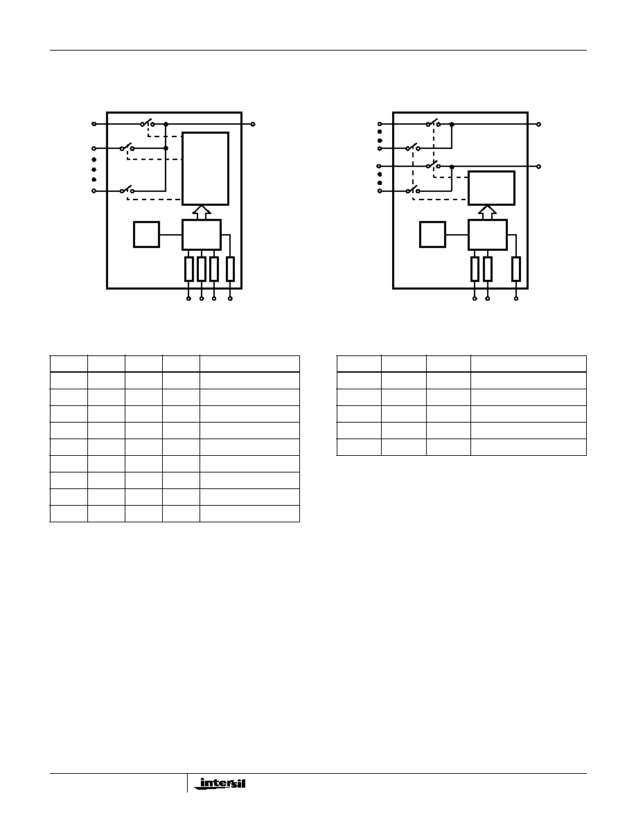
Burn-In/Life Test Circuits
HS-0508RH
DYNAMIC BURN-IN AND LIFE TEST CIRCUIT
V1 = -15V maximum, -16V minimum
V2 = +15V minimum, +16V maximum
R1 = 10k
±
5% 1/4W
C1 = C2 = 0.01
µ
F minimum (per socket) or 0.1
µ
F minimum (per row)
D1 = D2 = 1N4002 (or equivalent)
F0 = 100kHz 50% duty cycle; VIL = 0.8V max; VIH = 4.0V min.
F1 = F0/2
F2 = F1/2
F3 = F2/2
HS-0508RH
STATIC BURN-IN TEST CIRCUIT
V1 = 5V minimum, 6V maximum
V2 = -15V maximum, -16V minimum
V3 = +15V minimum, +16V maximum
R1 = 10k
±
5% 1/4W
C1 = C2 = 0.01
µ
F minimum (per socket) or 0.1
µ
F minimum (per row)
D1 = D2 = 1N4002 (or equivalent)
HS-0509RH
DYNAMIC BURN-IN AND LIFE TEST CIRCUIT
V2 = +15.5V,
±
.0.5V
V3 = -15.5V,
±
0.5V
R1 = 10k
,
±
5%
C1 = 0.1
µ
F minimum (per socket)
D1 = 1N4002 or equivalent (per board)
F0 = 100kHz,
±
10%; F1 = F0/2; F2 = F1/2, 50% duty cycle,
VIL = 0.8V max.; VIH = 4.0V min.
HS-0509RH
STATIC BURN-IN TEST CIRCUIT
V1 = +5.5V,
±
0.5V
V2 = +15.5V,
±
0.5V
V3 = -15.5V,
±
0.5V
R1 = 10k
,
±
10%
C1 = 0.1
µ
F minimum (per socket)
D1 = 1N4002 or equivalent (per board)
14
15
16
9
13
12
11
10
1
2
3
4
5
7
6
8
F0
F3
V1
D1
C1
R1
F1
F2
V2
D2
C2
14
15
16
9
13
12
11
10
1
2
3
4
5
7
6
8
V2
D1
C1
R1
V1
V3
D2
C2
14
15
16
9
13
12
11
10
1
2
3
4
5
7
6
8
F0
F2
V2
V3
D1
C1
R1
R1
D1
C1
F1
V2
V3
D1
C1
R1
R1
D1
C1
V1
14
15
16
9
13
12
11
10
1
2
3
4
5
7
6
8
HS-0508RH, HS-0509RH