1
File Number
4100.2
HS-1100RH
Radiation Hardened, Ultra High Speed
Current Feedback Amplifier
The HS-1100RH is a radiation hardened high speed,
wideband, fast settling current feedback amplifier. Built with
Intersil's proprietary, complementary bipolar UHF-1 (DI
bonded wafer) process, it is the fastest monolithic amplifier
available from any semiconductor manufacturer. These
devices are QML approved and are processed and screened
in full compliance with MIL-PRF-38535.
The HS-1100RH's wide bandwidth, fast settling characteristic,
and low output impedance make this amplifier ideal for driving
fast A/D converters.
Component and composite video systems will also benefit
from this amplifier's performance, as indicated by the
excellent gain flatness, and 0.03%/0.05 Deg. Differential
Gain/Phase specifications (R
L
= 75
).
Specifications for Rad Hard QML devices are controlled
by the Defense Supply Center in Columbus (DSCC). The
SMD numbers listed here must be used when ordering.
Detailed Electrical Specifications for these devices are
contained in SMD 5962-94676. A "hot-link" is provided
on our homepage for downloading.
http://www.intersil.com/spacedefense/space.htm
Features
∑ Electrically Screened to SMD # 5962-94676
∑ QML Qualified per MIL-PRF-38535 Requirements
∑ Low Distortion (HD3, 30MHz). . . . . . . . . . . . -84dBc (Typ)
∑ Wide -3dB Bandwidth. . . . . . . . . . . . . . . . . 850MHz (Typ)
∑ Very High Slew Rate . . . . . . . . . . . . . . . . 2300V/
µ
s (Typ)
∑ Fast Settling (0.1%) . . . . . . . . . . . . . . . . . . . . . 11ns (Typ)
∑ Excellent Gain Flatness (to 50MHz) . . . . . . . 0.05dB (Typ)
∑ High Output Current . . . . . . . . . . . . . . . . . . . 65mA (Typ)
∑ Fast Overdrive Recovery . . . . . . . . . . . . . . . . <10ns (Typ)
∑ Total Gamma Dose. . . . . . . . . . . . . . . . . . . . 300kRAD(Si)
∑ Latch Up . . . . . . . . . . . . . . . . . . . . . None (DI Technology)
Applications
∑ Video Switching and Routing
∑ Pulse and Video Amplifiers
∑ Wideband Amplifiers
∑ RF/IF Signal Processing
∑ Flash A/D Driver
∑ Imaging Systems
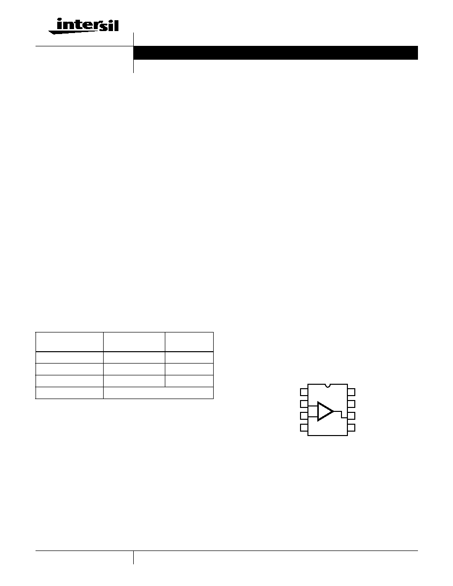
Pinout
HS-1100RH
GDIP1-T8 (CERDIP)
OR CDIP2-T8 (SBDIP)
TOP VIEW
Ordering Information
ORDERING NUMBER
INTERNAL
MKT. NUMBER
TEMP. RANGE
(
o
C)
5962F9467602VPA
HS7-1100RH-Q
-55 to 125
5962F9467602VPC
HS7B-1100RH-Q
-55 to 125
HFA1100IJ (Sample)
HFA1100IJ
-40 to 85
HFA11XXEVAL
Evaluation Board
NC
-IN
+IN
V-
1
2
3
4
8
7
6
5
NC
V+
OUT
NC
-
+
Data Sheet
August 1999
CAUTION: These devices are sensitive to electrostatic discharge; follow proper IC Handling Procedures.
1-888-INTERSIL or 321-724-7143 | Copyright © Intersil Corporation 1999
2
Typical Applications
Optimum Feedback Resistor
The enclosed plots of inverting and non-inverting frequency
response illustrate the performance of the HS-1100RH in
various gains. Although the bandwidth dependency on
closed loop gain isn't as severe as that of a voltage
feedback amplifier, there can be an appreciable decrease
in bandwidth at higher gains. This decrease may be
minimized by taking advantage of the current feedback
amplifier's unique relationship between bandwidth and R
F
.
All current feedback amplifiers require a feedback resistor,
even for unity gain applications, and R
F
, in conjunction with
the internal compensation capacitor, sets the dominant
pole of the frequency response. Thus, the amplifier's
bandwidth is inversely proportional to R
F
. The HS-1100RH
design is optimized for a 510
R
F
at a gain of +1.
Decreasing R
F
in a unity gain application decreases
stability, resulting in excessive peaking and overshoot. At
higher gains the amplifier is more stable, so R
F
can be
decreased in a trade-off of stability for bandwidth.
The table below lists recommended R
F
values for various
gains, and the expected bandwidth.
PC Board Layout
The frequency response of this amplifier depends greatly on
the amount of care taken in designing the PC board. The
use of low inductance components such as chip
resistors and chip capacitors is strongly recommended,
while a solid ground plane is a must!
Attention should be given to decoupling the power supplies.
A large value (10
µ
F) tantalum in parallel with a small value
(0.1
µ
F) chip capacitor works well in most cases.
Terminated microstrip signal lines are recommended at the
input and output of the device. Capacitance directly on the
output must be minimized, or isolated as discussed in the
next section.
Care must also be taken to minimize the capacitance to
ground seen by the amplifier's inverting input (-IN). The
larger this capacitance, the worse the gain peaking, resulting
in pulse overshoot and possible instability. To this end, it is
recommended that the ground plane be removed under
traces connected to -IN, and connections to -IN should be
kept as short as possible.
An example of a good high frequency layout is the
Evaluation Board shown in Figure 2.
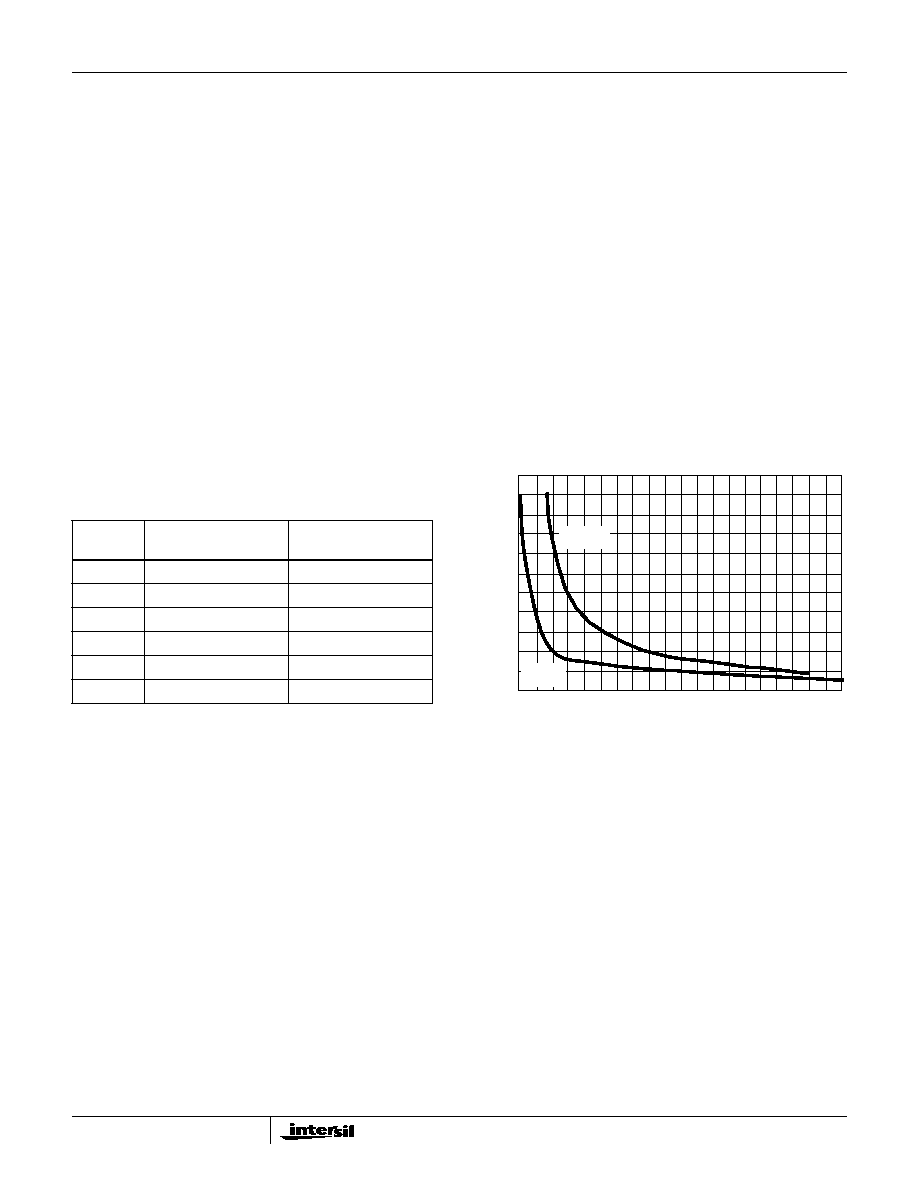
Driving Capacitive Loads
Capacitive loads, such as an A/D input, or an improperly
terminated transmission line will degrade the amplifier's
phase margin resulting in frequency response peaking and
possible oscillations. In most cases, the oscillation can be
avoided by placing a resistor (R
S
) in series with the output
prior to the capacitance.
Figure 1 details starting points for the selection of this
resistor. The points on the curve indicate the R
S
and C
L
combinations for the optimum bandwidth, stability, and
settling time, but experimental fine tuning is recommended.
Picking a point above or to the right of the curve yields an
overdamped response, while points below or left of the curve
indicate areas of underdamped performance.
R
S
and C
L
form a low pass network at the output, thus
limiting system bandwidth well below the amplifier bandwidth
of 850MHz. By decreasing R
S
as C
L
increases (as
illustrated in the curves), the maximum bandwidth is
obtained without sacrificing stability. Even so, bandwidth
does decrease as you move to the right along the curve. For
example, at A
V
= +1, R
S
= 50
, C
L
= 30pF, the overall
bandwidth is limited to 300MHz, and bandwidth drops to
100MHz at A
V
= +1, R
S
= 5
, C
L
= 340pF.
Evaluation Board
The performance of the HS-1100RH may be evaluated using
the HFA11XXEVAL Evaluation Board.
The layout and schematic of the board are shown in
Figure 2. To order evaluation boards, please contact your
local sales office.
GAIN
(ACL)
R
F
(
)
BANDWIDTH
(MHz)
-1
430
580
+1
510
850
+2
360
670
+5
150
520
+10
180
240
+19
270
125
R
S
(
)
LOAD CAPACITANCE (pF)
50
45
40
35
30
25
20
15
10
5
0
0
40
80
120
160
200
240
280
320
360 400
A
V
= +1
A
V
= +2
FIGURE 1. RECOMMENDED SERIES OUTPUT RESISTOR vs
LOAD CAPACITANCE
HS-1100RH
3
FIGURE 2A. TOP LAYOUT
FIGURE 2B. BOTTOM LAYOUT
FIGURE 2C. SCHEMATIC
FIGURE 2. EVALUATION BOARD SCHEMATIC AND LAYOUT
VH
+IN
VL
V+
GND
1
V-
OUT
1
2
3
4
8
7
6
5
+5V
10
µ
F
0.1
µ
F
V
H
50
GND
GND
R
1
-5V
0.1
µ
F
10
µ
F
50
IN
OUT
V
L
500
500
Typical Performance Characteristics
Device Characterized at: V
SUPPLY
=
±
5V, R
F
= 360
, A
V
= +2V/V, R
L
= 100
, Unless Otherwise Specified
PARAMETERS
CONDITIONS
TEMPERATURE
TYPICAL
UNITS
Input Offset Voltage (Note 1)
V
CM
= 0V
25
o
C
2
mV
Average Offset Voltage Drift
Versus Temperature
Full
10
µ
V/
o
C
V
IO
CMRR
V
CM
=
±
2V
25
o
C
46
dB
V
IO
PSRR
V
S
=
±
1.25V
25
o
C
50
dB
+Input Current (Note 1)
V
CM
= 0V
25
o
C
25
µ
A
Average +Input Current Drift
Versus Temperature
Full
40
nA/
o
C
- Input Current (Note 1)
V
CM
= 0V
25
o
C
12
µ
A
Average -Input Current Drift
Versus Temperature
Full
40
nA/
o
C
+Input Resistance
V
CM
=
±
2V
25
o
C
50
k
- Input Resistance
25
o
C
16
Input Capacitance
25
o
C
2.2
pF
Input Noise Voltage (Note 1)
f = 100kHz
25
o
C
4
nV/
Hz
+Input Noise Current (Note 1)
f = 100kHz
25
o
C
18
pA/
Hz
-Input Noise Current (Note 1)
f = 100kHz
25
o
C
21
pA/
Hz
Input Common Mode Range
Full
±
3.0
V
Open Loop Transimpedance
A
V
= -1
25
o
C
500
k
HS-1100RH
4
Output Voltage
A
V
= -1, R
L
= 100
25
o
C
±
3.3
V
A
V
= -1, R
L
= 100
Full
±
3.0
V
Output Current (Note 1)
A
V
= -1, R
L
= 50
25
o
C to 125
o
C
±
65
mA
A
V
= -1, R
L
= 50
-55
o
C to 0
o
C
±
50
mA
DC Closed Loop Output Resistance
25
o
C
0.1
W
Quiescent Supply Current (Note 1)
R
L
= Open
Full
24
mA
-3dB Bandwidth (Note 1)
A
V
= -1, R
F
= 430
, V
OUT
= 200mV
P-P
25
o
C
580
MHz
A
V
= +1, R
F
= 510
, V
OUT
= 200mV
P-P
25
o
C
850
MHz
A
V
= +2, R
F
= 360
, V
OUT
= 200mV
P-P
25
o
C
670
MHz
Slew Rate
A
V
= +1, R
F
= 510
, V
OUT
= 5V
P-P
25
o
C
1500
V/
µ
s
A
V
= +2, V
OUT
= 5V
P-P
25
o
C
2300
V/
µ
s
Full Power Bandwidth
V
OUT
= 5V
P-P
25
o
C
220
MHz
Gain Flatness (Note 1)
To 30MHz, R
F
= 510
25
o
C
±
0.014
dB
To 50MHz, R
F
= 510
25
o
C
±
0.05
dB
To 100MHz, R
F
= 510
25
o
C
±
0.14
dB
Linear Phase Deviation (Note 1)
To 100MHz, R
F
= 510
25
o
C
±
0.6
Degrees
2nd Harmonic Distortion (Note 1)
30MHz, V
OUT
= 2V
P-P
25
o
C
-55
dBc
50MHz, V
OUT
= 2V
P-P
25
o
C
-49
dBc
100MHz, V
OUT
= 2V
P-P
25
o
C
-44
dBc
3rd Harmonic Distortion (Note 1)
30MHz, V
OUT
= 2V
P-P
25
o
C
-84
dBc
50MHz, V
OUT
= 2V
P-P
25
o
C
-70
dBc
100MHz, V
OUT
= 2V
P-P
25
o
C
-57
dBc
3rd Order Intercept (Note 1)
100MHz, R
F
= 510
25
o
C
30
dBm
1dB Compression
100MHz, R
F
= 510
25
o
C
20
dBm
Reverse Isolation (S12)
40MHz, R
F
= 510
25
o
C
-70
dB
100MHz, R
F
= 510
25
o
C
-60
dB
600MHz, R
F
= 510
25
o
C
-32
dB
Rise and Fall Time
V
OUT
= 0.5V
P-P
25
o
C
500
ps
V
OUT
= 2V
P-P
25
o
C
800
ps
Overshoot (Note 1)
V
OUT
= 0.5V
P-P
, Input t
R
/t
F
= 550ps
25
o
C
11
%
Settling Time (Note 1)
To 0.1%, V
OUT
= 2V to 0V, R
F
= 510
25
o
C
11
ns
To 0.05%, V
OUT
= 2V to 0V, R
F
= 510
25
o
C
19
ns
To 0.02%, V
OUT
= 2V to 0V, R
F
= 510
25
o
C
34
ns
Differential Gain
A
V
= +2, R
L
= 75
, NTSC
25
o
C
0.03
%
Differential Phase
A
V
= +2, R
L
= 75
, NTSC
25
o
C
0.05
Degrees
Overdrive Recovery Time
R
F
= 510
, V
IN
= 5V
P-P
25
o
C
7.5
ns
NOTE:
1. See Typical Performance Curves for more information.
Typical Performance Characteristics
(Continued)
Device Characterized at: V
SUPPLY
=
±
5V, R
F
= 360
, A
V
= +2V/V, R
L
= 100
, Unless Otherwise Specified
PARAMETERS
CONDITIONS
TEMPERATURE
TYPICAL
UNITS
HS-1100RH
5
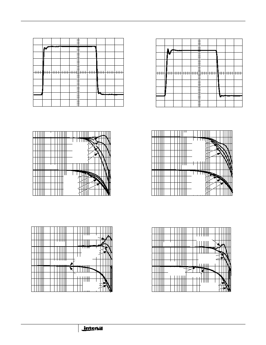
Typical Performance Curves
V
SUPPLY
=
±
5V, R
F
= 510
, R
L
= 100
, T
A
= 25
o
C, Unless Otherwise Specified
FIGURE 3. SMALL SIGNAL PULSE RESPONSE (A
V
= +2)
FIGURE 4. LARGE SIGNAL PULSE RESPONSE (A
V
= +2)
FIGURE 5. NON-INVERTING FREQUENCY RESPONSE
(V
OUT
= 200mV
P-P
)
FIGURE 6. INVERTING FREQUENCY RESPONSE
(V
OUT
= 200mV
P-P
)
FIGURE 7. FREQUENCY RESPONSE FOR VARIOUS LOAD
RESISTORS (A
V
= +1, V
OUT
= 200mV
P-P
)
FIGURE 8. FREQUENCY RESPONSE FOR VARIOUS LOAD
RESISTORS (A
V
= +2, V
OUT
= 200mV
P-P
)
120
5ns/DIV.
90
60
30
0
-30
-60
-90
-120
OUTPUT V
O
L
T
A
GE (mV)
5ns/DIV.
OUTPUT V
O
L
T
A
GE (V)
1.2
0.9
0.6
0.3
0
-0.3
-0.6
-0.9
-1.2
FREQUENCY (MHz)
0
-3
-6
-9
-12
GAIN (dB) NORMALIZED
0.3
1
10
100
1K
0
-90
-180
-270
-360
PHASE
GAIN
A
V
= +1
A
V
= +11
A
V
= +2
A
V
= +6
PHASE (DEGREES)
A
V
= +1
A
V
= +11
A
V
= +2
A
V
= +6
FREQUENCY (MHz)
PHASE
GAIN
0
-3
-6
-9
-12
GAIN (dB) NORMALIZED
0.3
1
10
100
1K
180
90
0
-90
-180
A
V
= -1
A
V
= -1
A
V
= -20
A
V
= -5
A
V
= -10
A
V
= -20
A
V
= -5
A
V
= -10
PHASE (DEGREES)
FREQUENCY (MHz)
+6
+3
0
-3
-6
GAIN (dB)
0.3
1
10
100
1K
0
-90
-180
-270
-360
PHASE
GAIN
R
L
= 1k
R
L
= 100
R
L
= 50
R
L
= 1k
PHASE (DEGREES)
R
L
= 50
R
L
= 100
R
L
= 1k
R
L
= 100
FREQUENCY (MHz)
PHASE
GAIN
+3
0
-3
-6
GAIN (dB) NORMALIZED
0.3
1
10
100
1K
0
-90
-180
-270
-360
PHASE (DEGREES)
R
L
= 100
R
L
= 1k
R
L
= 50
R
L
= 100
R
L
= 1k
R
L
= 50
R
L
= 100
R
L
= 1k
HS-1100RH