
1
CAUTION: These devices are sensitive to electrostatic discharge; follow proper IC Handling Procedures.
www.intersil.com or 407-727-9207
|
Copyright
©
Intersil Corporation 1999
Satellite Applications FlowTM (SAF) is a trademark of Intersil Corporation.
HS-6617RH-T
Radiation Hardened 2K x 8 CMOS PROM
Intersil's Satellite Applications Flow
TM
(SAF) devices are fully
tested and guaranteed to 100kRAD total dose. These QML
Class T devices are processed to a standard flow intended
to meet the cost and shorter lead-time needs of large
volume satellite manufacturers, while maintaining a high
level of reliability.
The Intersil HS-6617RH-T is a radiation hardened 16k
CMOS PROM, organized in a 2K word by 8-bit format. The
chip is manufactured using a radiation hardened CMOS
process, and is designed to be functionally equivalent to the
HM-6617. Synchronous circuit design techniques combine
with CMOS processing to give this device high speed
performance with very low power dissipation.
On chip address latches are provided, allowing easy
interfacing with recent generation microprocessors that use
multiplexed address/data bus structure, such as the
HS-80C86RH. The output enable control (G) simplifies
microprocessor system interfacing by allowing output data
bus control, in addition to, the chip enable control.
Synchronous operation of the HS-6617RH-T is ideal for high
speed pipe-lined architecture systems and also in
synchronous logic replacement functions.
Specifications
Specifications for Rad Hard QML devices are controlled by
the Defense Supply Center in Columbus (DSCC). The SMD
numbers listed below must be used when ordering.
Detailed Electrical Specifications for the HS-6617RH-T
are contained in SMD 5962-95708. A "hot-link" is provided
from our website for downloading.
www.intersil.com/spacedefense/newsafclasst.asp
Intersil's Quality Management Plan (QM Plan), listing all
Class T screening operations, is also available on our
website.
www.intersil.com/quality/manuals.asp
Features
∑ QML Class T, Per MIL-PRF-38535
∑ Radiation Performance
- Gamma Dose (
) 1 x 10
5
RAD(Si)
- SEU LET 16MeV/mg/cm
2
- SEL LET 100MeV/mg/cm
2
∑ Field Programmable Nicrome Fuse Links
∑ Low Standby Power 1.1mW Max
∑ Low Operating Power 137.5mW/MHz Max
∑ Fast Access Time 100ns Max
∑ TTL Compatible Inputs/Outputs
∑ Synchronous Operation
∑ On Chip Address Latches, Three-State Outputs
Pinouts
HS1-6617RH-T (SBDIP), CDIP2-T24
TOP VIEW
HS9-6617RH-T (FLATPACK), CDFP4-F24
TOP VIEW
Ordering Information
ORDERING
NUMBER
PART NUMBER
TEMP.
RANGE
(
o
C)
5962R9570801TJC
HS1-6617RH-T
-55 to 125
HS1-6617RH/Proto
HS1-6617RH/Proto
-55 to 125
5962R9570801TXC
HS9-6617RH-T
-55 to 125
HS9-6617RH/Proto
HS9-6617RH/Proto
-55 to 125
NOTE:
Minimum order quantity for -T is 150 units through
distribution, or 450 units direct.
1
2
3
4
5
6
7
8
9
10
11
12
A7
A6
A5
A4
A3
A2
A1
A0
Q0
Q1
Q2
GND
16
17
18
19
20
21
22
23
24
15
14
13
V
DD
A9
P
G
A10
Q7
Q5
Q4
Q3
A8
E
Q6
A7
A6
A5
A4
A3
A2
A1
A0
Q0
Q1
Q2
GND
V
DD
A8
A9
P
G
A10
E
Q7
Q6
Q5
Q4
Q3
2
3
4
5
6
7
8
9
10
11
12
1
24
23
22
21
20
19
18
17
16
15
14
13
P must be hardwired at all times to V
DD
, except during
programming.
Data Sheet
July 1999
File Number
4608.1
3
All Intersil semiconductor products are manufactured, assembled and tested under ISO9000 quality systems certification.
Intersil semiconductor products are sold by description only. Intersil Corporation reserves the right to make changes in circuit design and/or specifications at any time with-
out notice. Accordingly, the reader is cautioned to verify that data sheets are current before placing orders. Information furnished by Intersil is believed to be accurate and
reliable. However, no responsibility is assumed by Intersil or its subsidiaries for its use; nor for any infringements of patents or other rights of third parties which may result
from its use. No license is granted by implication or otherwise under any patent or patent rights of Intersil or its subsidiaries.
For information regarding Intersil Corporation and its products, see web site http://www.intersil.com
Die Characteristics
DIE DIMENSIONS:
(4166
µ
m x 6350
µ
m x 483
µ
m
±
25.4
µ
m)
164 x 250 x 19mils
±
1mil
METALLIZATION:
Type: Silicon - Aluminum
Thickness: 13.0k
≈
±
2k
≈
SUBSTRATE POTENTIAL:
V
DD
BACKSIDE FINISH:
Silicon
PASSIVATION:
Type: Silox (S
i
O
2
)
Thickness: 8.0k
≈
±
1k
≈
WORST CASE CURRENT DENSITY:
< 2.0e5 A/cm
2
PROCESS:
SSAJIIV-RH
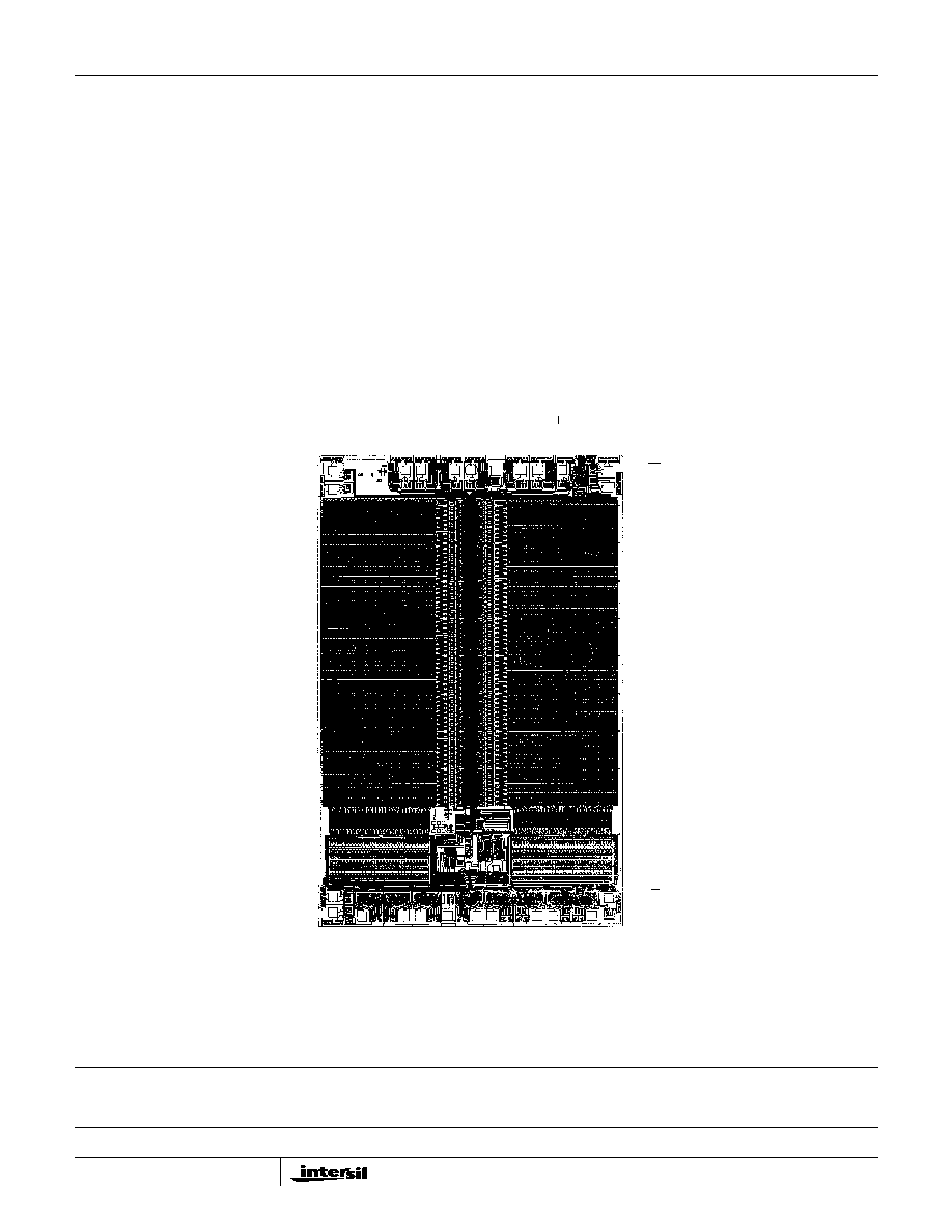
Metallization Mask Layout
HS-6617RH-T
A2 (6)
A1 (7)
A0 (8)
Q0 (9)
Q1 (10)
Q2 (11)
GND (12)
Q3 (13)
Q4 (14)
Q5 (15)
Q6 (16)
Q7 (17)
(20) G
(19) A10
(18) E
(5) A3
(4) A4
(3)A5
(2) A6
(1) A7
(24)V
DD
(23) A8
(22) A9
(21)
P
HS-6617RH-T
