1
CAUTION: These devices are sensitive to electrostatic discharge; follow proper IC Handling Procedures.
http://www.intersil.com or 407-727-9207
|
Copyright
©
Intersil Corporation 1999
HS-80C85RH
Radiation Hardened
8-Bit CMOS Microprocessor
Description
The HS-80C85RH is an 8-bit CMOS microprocessor fabri-
cated using the Intersil radiation hardened self-aligned junc-
tion isolated (SAJI) silicon gate technology. Latch-up free
operation is achieved by the use of epitaxial starting material
to eliminate the parasitic SCR effect seen in conventional
bulk CMOS devices.
The HS-80C85RH is a functional logic emulation of the
HMOS 8085 and its instruction set is 100% software com-
patible with the HMOS device. The HS80C85RH is designed
for operation with a single 5 volt power supply. Its high level
of integration allows the construction of a radiation hardened
microcomputer system with as few as three ICs (HS-
80C85RH CPU, HS83C55RH ROM I/O, and the HS-81C55/
56RH RAM I/O.
Features
∑ Devices QML Qualified in Accordance With
MIL-PRF-38535
∑ Detailed Electrical and Screening Requirements are
Contained in SMD# 5962-95824 and Intersil' QM Plan
∑ Radiation Hardened EPI-CMOS
- Parametrics Guaranteed 1 x 10
5
RAD(Si)
- Transient Upset > 1 x 10
8
RAD(Si)/s
- Latch-up Free > 1 x 10
12
RAD(Si)/s
∑ Low Standby Current 500
µ
A Max
∑ Low Operating Current 5.0mA/MHz (X
1
Input)
∑ Electrically Equivalent to Sandia SA 3000
∑ 100% Software Compatible with INTEL 8085
∑ Operation from DC to 2MHz, Post Radiation
∑ Single 5 Volt Power Supply
∑ On-Chip Clock Generator and System Controller
∑ Four Vectored Interrupt Inputs
∑ Completely Static Design
∑ Self Aligned Junction Isolated (SAJI) Process
∑ Military Temperature Range -55
o
C to +125
o
C
February 1996
Spec Number
518054
File Number
3036.2
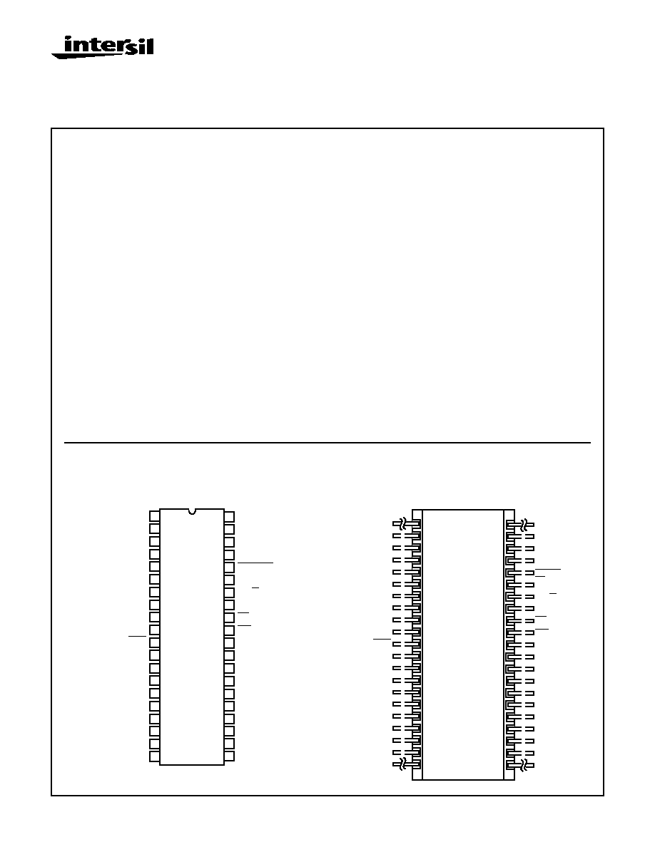
Pinouts
40 LEAD CERAMIC DUAL-IN-LINE
METAL SEAL PACKAGE (SBDIP)
MIL-STD-1835, CDIP2-T40
TOP VIEW
42 LEAD CERAMIC METAL SEAL
FLATPACK PACKAGE (FLATPACK)
INTERSIL OUTLINE K42.A
TOP VIEW
33
34
35
36
37
38
39
40
32
31
30
29
24
25
26
27
28
21
22
23
HLDA
HOLD
READY
RD
IO / M
ALE
WR
VDD
S1
S0
A15
A14
A13
A12
A11
A10
A9
A8
13
1
2
3
4
5
6
7
8
9
10
11
12
14
15
16
17
18
19
20
INTR
INTA
SOD
SID
TRAP
RST 7.5
RST 6.5
RST 5.5
GND
X1
X2
AD0
AD1
AD2
AD3
AD4
AD5
AD6
AD7
RESET OUT
RESET IN
CLOCK OUT
HLDA
HOLD
READY
RD
IO / M
ALE
WR
VDD
S1
S0
A15
A14
A13
A12
A11
A10
A9
A8
RESET
CLOCK
GND
OUT
IN
INTR
INTA
SOD
SID
TRAP
RST 7.5
RST 6.5
RST 5.5
X1
X2
AD0
AD1
AD2
AD3
AD4
AD5
AD6
AD7
RESET
OUT
NC
NC
33
32
39
38
37
36
35
34
42
41
31
30
29
28
27
24
23
22
40
26
25
10
11
4
5
6
7
8
9
1
2
12
13
14
15
16
19
20
21
3
17
18

2
HS-80C85RH
Functional Diagram
Ordering Information
PART NUMBER
TEMPERATURE RANGE
SCREENING LEVEL
PACKAGE
5962R9582401QQC
-55
o
C to +125
o
C
MIL-PRF-38535 Level Q
40 Lead SBDIP
5962R9582401QXC
-55
o
C to +125
o
C
MIL-PRF-38535 Level Q
42 Lead Ceramic Flatpack
5962R9582401VQC
-55
o
C to +125
o
C
MIL-PRF-38535 Level V
40 Lead SBDIP
5962R9582401VXC
-55
o
C to +125
o
C
MIL-PRF-38535 Level V
42 Lead Ceramic Flatpack
HS1-80C85RH/SAMPLE
+25
o
C
Sample
40 Lead SBDIP
HS9-80C85RH/SAMPLE
+25
o
C
Sample
42 Lead Ceramic Flatpack
ACCUMU-
LATOR (8)
TEMP REG
(8)
FLAG (5)
FLIP FLOPS
INSTRUCTION
REGISTER (8)
ARITHMETIC
LOGIC
UNIT
(ALU) (8)
POWER
SUPPLY
VDD
GND
INSTRUCTION
DECODER
AND MACHINE
CYCLE
ENCODING
X1
X2
CLK
GEN
CONTROL
STATUS
DMA
RESET
TIMING AND CONTROL
ADDRESS
A15-A8
CLK
OUT
READY
RD
WR
ALE
S0
S1
IO/M
HLDA
RESET
IN
RESET
OUT
HOLD
BUFFER (8)
ADDRESS
BUS
B REG (8)
D REG (8)
H REG (8)
STACK POINTER (16)
C REG (8)
E REG (8)
L REG (8)
PROGRAM COUNTER (16)
INCREMENTER
ADDRESS LATCH (16)
DECREMENTER
DATA ADDRESS
BUFFER (8)
AD1-AD0
ADDRESS
BUS
INTERRUPT CONTROL
SERIAL I/O CONTROL
8-BIT
INTERNAL DATA BUS
INTA
INTR
RST
TRAP
SID
SOD
5.5
RST
6.5
RST
7.5
REGISTER ARRA
Y
Spec Number
518054
3
HS-80C85RH
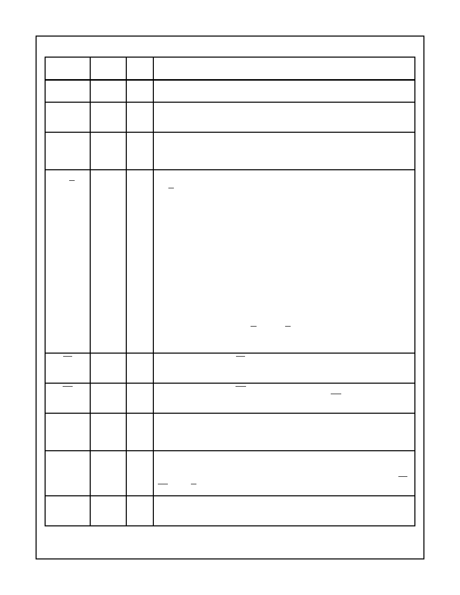
Pin Description
SYMBOL
PIN
NUMBER
TYPE
DESCRIPTION
A8 - A15
21-28
O
Address Bus: The most significant 8 bits of the memory address or the 8 bits of the I/O address,
3-stated during Hold and Halt modes and during RESET.
AD0-7
12-19
I/O
Multiplexed Address/Data Bus: Lower 8 bits of the memory address (or I/O address) appear on
the bus during the first clock cycle (T state) of a machine cycle. It then becomes the data bus
during the second and third clock cycles.
ALE
32
O
Address Latch Enable: It occurs during the first clock state of a machine cycle and enables the
address to get latched into the on-chip latch of peripherals. The falling edge of ALE is set to guar-
antee setup and hold times for the address information. The falling edge of ALE can also be used
to strobe the status information. ALE is never 3-stated.
S0, S1, and
IO/M
31, 35,
& 36
O
Machine Cycle Status:
IO/M
S1
S0
Status
0
0
1
Memory write
0
1
0
Memory write
1
0
1
I/O write
1
1
0
I/O read
0
1
1
Opcode fetch
1
1
1
Opcode fetch
1
1
1
Interrupt acknowledge
T
0
0
Halt
T
X
X
Hold
T
X
X
Reset
T = 3-State (high impedance)
X = Unspecified
S1 can be used as an advanced R/W status. IO/M, S0 and S1 become valid at the beginning of
a machine cycle and remain stable throughout the cycle. The falling edge of ALE may be used
to latch the state of these lines.
RD
34
O
Read Control: A low level on RD indicates the selected memory or I/O device is to be read and
that the Data Bus is available for the data transfer, 3-stated during Hold and Halt modes and dur-
ing RESET.
WR
33
O
Write Control: A low level on WR indicates the data on the Data Bus is to be written into the se-
lected memory or I/O location. Data is set up at the trailing edge of WR, 3-stated during Hold and
Halt modes and during RESET.
READY
35
I
Ready: If READY is high during a read or write cycle, it indicates that the memory or peripheral
is ready to send or receive data. If READY is low, the cpu will wait an integral number of clock
cycles for READY to go high before completing the read or write cycle. READY must conform to
specified setup and hold times.
HOLD
39
I
Hold: Indicates that another master is requesting the use of the address and data buses. The
cpu, upon receiving the hold request, will relinquish the use of the bus as soon as the completion
of the current bus transfer. Internal processing can continue. The processor can regain the bus
only after the HOLD is removed. When the HOLD is acknowledged, the Address, Data Bus, RD,
WR, and IO/M lines are 3-stated.
HLDA
38
O
Hold Acknowledge: Indicates that the cpu has received the HOLD request and that it will relin-
quish the bus in the next clock cycle. HLDA goes low after the Hold request is removed. The cpu
takes the bus one half clock cycle after HLDA goes low.
Spec Number
518054
4
HS-80C85RH
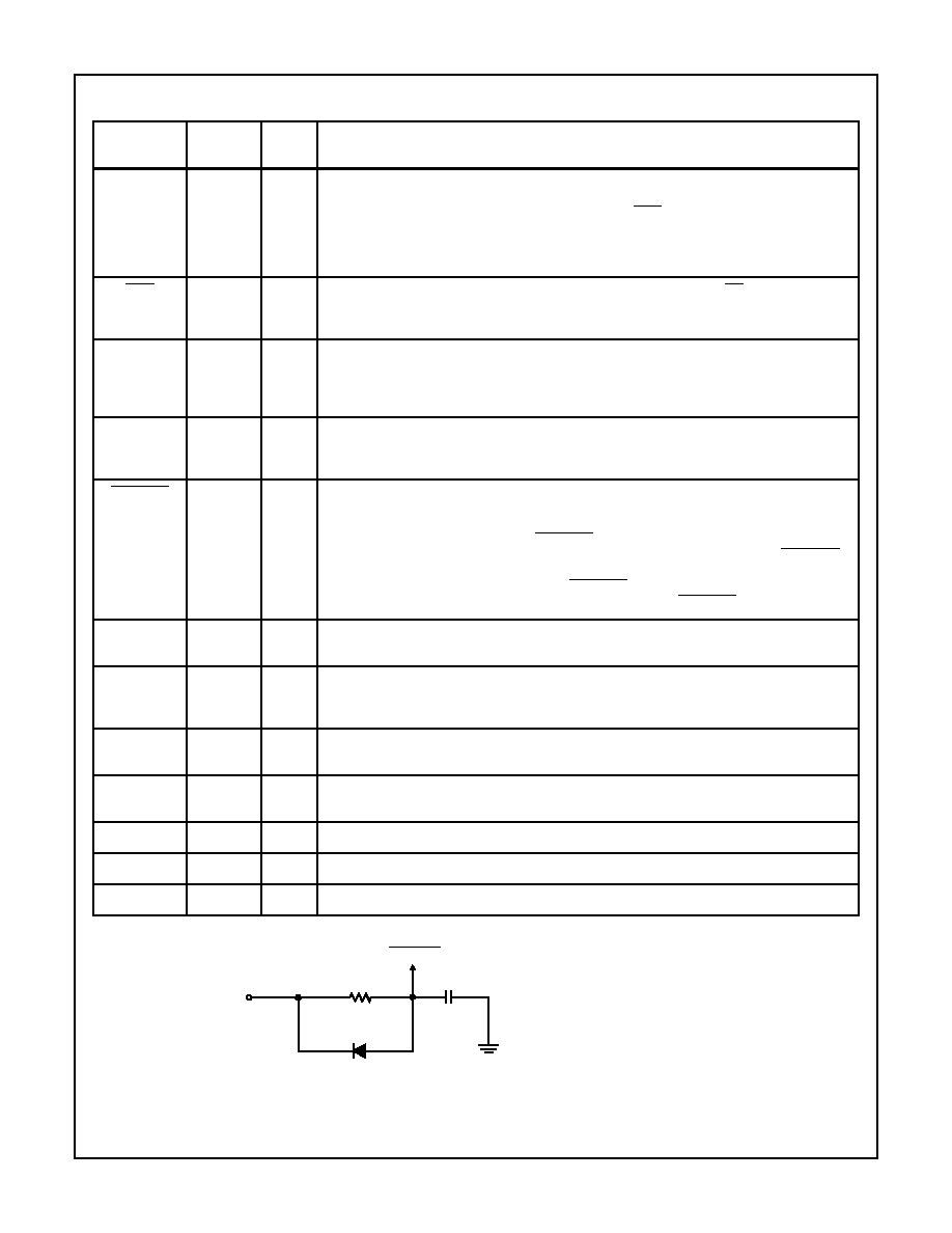
FIGURE 1. POWER-ON RESET CIRCUIT
INTR
10
I
Interrupt Request: Is used as a general purpose interrupt. It is sampled only during the next to
the last clock cycle of an instruction and during Hold and Halt states. If it is active, the Program
Counter (PC) will be inhibited from incrementing and an INTA will be issued. During this cycle a
RESTART or CALL instruction can be inserted to jump to the interrupt service routine. The INTR
is enabled and disabled by software. It is disabled by Reset and immediately after an interrupt is
accepted.
INTA
11
O
Interrupt Acknowledge: Is used instead of (and has the same timing as) RD during the Instruc-
tion cycle after an INTR is accepted. It can be used to activate an 8259A Interrupt chip or some
other interrupt port.
RST 5.5
RST 6.5
RST 7.5
9
8
7
I
Restart Interrupts: These three inputs have the same timing as INTR except they cause an
internal RESTART to be automatically inserted.
The priority of these interrupts is ordered as shown in Table 6. These interrupts have a higher
priority than INTR. In addition, they may be individually masked out using the SIM instruction.
TRAP
6
I
Trap: Trap interrupt is a non-maskable RESTART interrupt. It is recognized at the same time as
INTR or RST 5.5-7.5. It is unaffected by any mask or Interrupt Enable. It has the highest priority
of any interrupt. (See Table 6.)
RESET IN
36
I
Reset In: Sets the Program Counter to zero and resets the Interrupt Enable and HLDA flip-flops.
The data and address buses and the control lines are 3-stated during RESET and because of
the asynchronous nature of RESET the processor's internal registers and flags may be altered
by RESET with unpredictable results. RESET IN is a Schmitt-triggered input, allowing connec-
tion to an R-C network for power-on RESET delay (see Figure 1). Upon power-up, RESET IN
must remain low for at least 10 "clock cycle" after minimum VDD has been reached. For proper
reset operation after the power-up duration, RESET IN should be kept low a minimum of three
clock periods. The CPU is held in the reset condition as long as RESET IN is applied.
RESET OUT
3
O
Reset Out: Reset Out indicates cpu is being reset. Can be used as a system reset. The signal
is synchronized to the processor clock and lasts an integral number of clock periods.
X1
X2
1
2
I
O
X1 and X2: Are connected to a crystal, LC, or RC network to drive the internal clock generator.
X, can also be an external clock Input from a logic gate. The input frequency is divided by 2 to
give the processor's internal operating frequency.
CLK
37
O
Clock: Clock output for use as a system clock. The period of CLK is twice the X1, X2 input
period.
SID
5
I
Serial Input Data Line: The data on this line is loaded into accumulator bit 7 whenever a RIM
instruction is executed.
SOD
4
O
Serial Output Data Line: The output SOD is set or reset as specified by the SlM instruction.
VCC
40
I
Power: +5V supply.
GND
20
I
Ground: Reference.
Pin Description
(Continued)
SYMBOL
PIN
NUMBER
TYPE
DESCRIPTION
R1
VDD
RESET IN
C1
TYPICAL POWER-ON RESET RC VALUES
R1 = 75K
C1 = 1
µ
F
Values may have to vary due to applied power supply ramp up time.
Spec Number
518054
5
Specifications HS-80C85RH
Absolute Maximum Ratings
Reliability Information
Supply Voltage . . . . . . . . . . . . . . . . . . . . . . . . . . . . . . . . . . . . . +7.0V
Input, Output or I/O Voltage . . . . . . . . . . . . GND-0.3V to VCC+0.3V
Storage Temperature Range . . . . . . . . . . . . . . . . . -65
o
C to +150
o
C
Junction Temperature . . . . . . . . . . . . . . . . . . . . . . . . . . . . . . +175
o
C
Lead Temperature (Soldering 10s) . . . . . . . . . . . . . . . . . . . . +300
o
C
Typical Derating Factor. . . . . . . . . . .2.0mA/MHz Increase in IDDOP
ESD Classification . . . . . . . . . . . . . . . . . . . . . . . . . . . . . . . . Class 1
Thermal Resistance
JA
JC
SBDIP Package. . . . . . . . . . . . . . . . . . . .
45
o
C/W
10
o
C/W
Ceramic Flatpack Package . . . . . . . . . . .
77
o
C/W
13
o
C/W
Maximum Package Power Dissipation at +125
o
C Ambient
SBDIP Package. . . . . . . . . . . . . . . . . . . . . . . . . . . . . . . . . . 1.11W
Ceramic Flatpack Package . . . . . . . . . . . . . . . . . . . . . . . . . 0.65W
If device power exceeds package dissipation capability, provide heat
sinking or derate linearly at the following rate:
SBDIP Package. . . . . . . . . . . . . . . . . . . . . . . . . . . . . . 22.2mW/
o
C
Ceramic Flatpack Package . . . . . . . . . . . . . . . . . . . . . 13.0mW/
o
C
CAUTION: Stresses above those listed in "Absolute Maximum Ratings" may cause permanent damage to the device. This is a stress only rating and operation
of the device at these or any other conditions above those indicated in the operational sections of this specification is not implied.
Operating Conditions
Operating Supply Voltage Range (VDD) . . . . . . . +4.75V to +5.25V
Operating Temperature Range (T
A
) . . . . . . . . . . . . -55
o
C to +125
o
C
Input Low Voltage . . . . . . . . . . . . . . . . . . . . . . . . . . . . . .0V to +0.8V
Input High Voltage. . . . . . . . . . . . . . . . . . . . . . . . VDD -0.5V to VDD
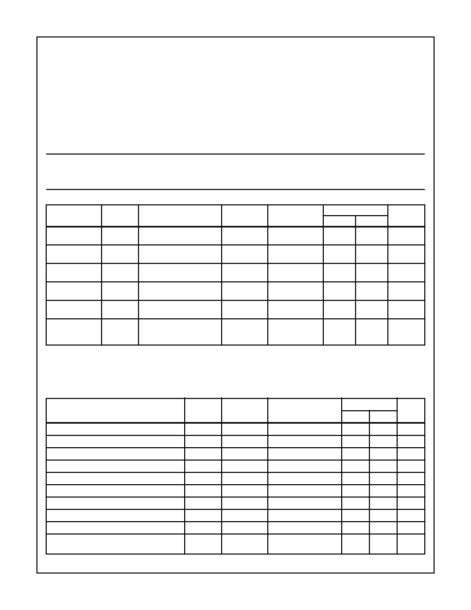
TABLE 1. DC ELECTRICAL PERFORMANCE CHARACTERISTICS
PARAMETER
SYMBOL
CONDITIONS
GROUP A
SUBGROUPS
TEMPERATURE
LIMITS
UNITS
MIN
MAX
Input Leakage
Current
IIH or
IIL
VDD = 5.25V, VI = VDD
or GND
1, 2, 3
-55
o
C, +25
o
C, or
+125
o
C
-1.0
1.0
µ
A
High Level Output
Voltage
VOH
VDD = 4.75V, IOH = -1.0mA
1, 2, 3
-55
o
C, +25
o
C, or
+125
o
C
VDD -0.5
-
V
Low Level Output
Voltage
VOL
VDD = 5.25V, IOL = 1.0mA,
1, 2, 3
-55
o
C, +25
o
C, or
+125
o
C
-
0.5
V
Static Current
IDDSB
VDD = 5.25V, Clock Out = Hi
and Low
1, 2, 3
-55
o
C, +25
o
C, or
+125
o
C
-
500
µ
A
Operating Supply
Current (Note 2)
IDDOP
VDD = 5.25V, f = 1MHz
(Note 2)
1, 2, 3
-55
o
C, +25
o
C, or
+125
o
C
-
5.0
mA/MHz
Functional Tests
FT
VDD = 4.75V and 5.25V,
TCYC = 500ns,
VOL
VDD/2, VOH
VDD/2
7, 8A, 8B
-55
o
C, +25
o
C, or
+125
o
C
-
-
-
NOTES:
1. All devices guaranteed at worst case limits and over radiation.
2. Operating supply current (IDDOP) is proportional to crystal frequency. Parts are tested at 1MHz
TABLE 2. AC ELECTRICAL PERFORMANCE CHARACTERISTICS
PARAMETER
SYMBOL
GROUP A
SUBGROUPS
TEMPERATURE
LIMITS
UNITS
MIN
MAX
CLK Low Time (Standard CLK Loading)
T1
9, 10, 11
-55
o
C, +25
o
C, +125
o
C
40
-
ns
CLK High Time (Standard CLK Loading)
T2
9, 10, 11
-55
o
C, +25
o
C, +125
o
C
100
-
ns
CLK Rise Time
Tr
9, 10, 11
-55
o
C, +25
o
C, +125
o
C
-
115
ns
CLK Fall Time
Tf
9, 10, 11
-55
o
C, +25
o
C, +125
o
C
-
115
ns
X1 Rising to CLK Rising
TXKR
9, 10, 11
-55
o
C, +25
o
C, +125
o
C
30
250
ns
X1 Rising to CLK Falling
TXKF
9, 10, 11
-55
o
C, +25
o
C, +125
o
C
50
275
ns
A8-15 Valid to Leading Edge of Control (Note 5)
TAC
9, 10, 11
-55
o
C, +25
o
C, +125
o
C
300
-
ns
A0-7 Valid to Leading Edge of Control
TACL
9, 10, 11
-55
o
C, +25
o
C, +125
o
C
300
-
ns
A0-15 Valid to Valid Data In
TAD
9, 10, 11
-55
o
C, +25
o
C, +125
o
C
875
-
ns
Address Float After Leading Edge of READ
(INTA)
TAFR
9, 10, 11
-55
o
C, +25
o
C, +125
o
C
-
70
ns
Spec Number
518054