1
CAUTION: These devices are sensitive to electrostatic discharge; follow proper IC Handling Procedures.
http://www.intersil.com or 407-727-9207
|
Copyright
©
Intersil Corporation 1999
Ordering Information
PART NUMBER
TEMPERATURE RANGE
SCREENING LEVEL
PACKAGE
5962R9582501QEC
-55
o
C to +125
o
C
MIL-PRF-38535 Level Q
16 Lead SBDIP
5962R9582501QXC
-55
o
C to +125
o
C
MIL-PRF-38535 Level Q
16 Lead Ceramic Flatpack
5962R9582501VEC
-55
o
C to +125
o
C
MIL-PRF-38535 Level V
16 Lead SBDIP
5962R9582501VXC
-55
o
C to +125
o
C
MIL-PRF-38535 Level V
16 Lead Ceramic Flatpack
HS1-54C138RH/SAMPLE
+25
o
C
Sample
16 Lead SBDIP
HS9-54C138RH/SAMPLE
+25
o
C
Sample
16 Lead Ceramic Flatpack
HS-54C138RH
Radiation Hardened
3-Line to 8-Line Decoder/Demultiplexer
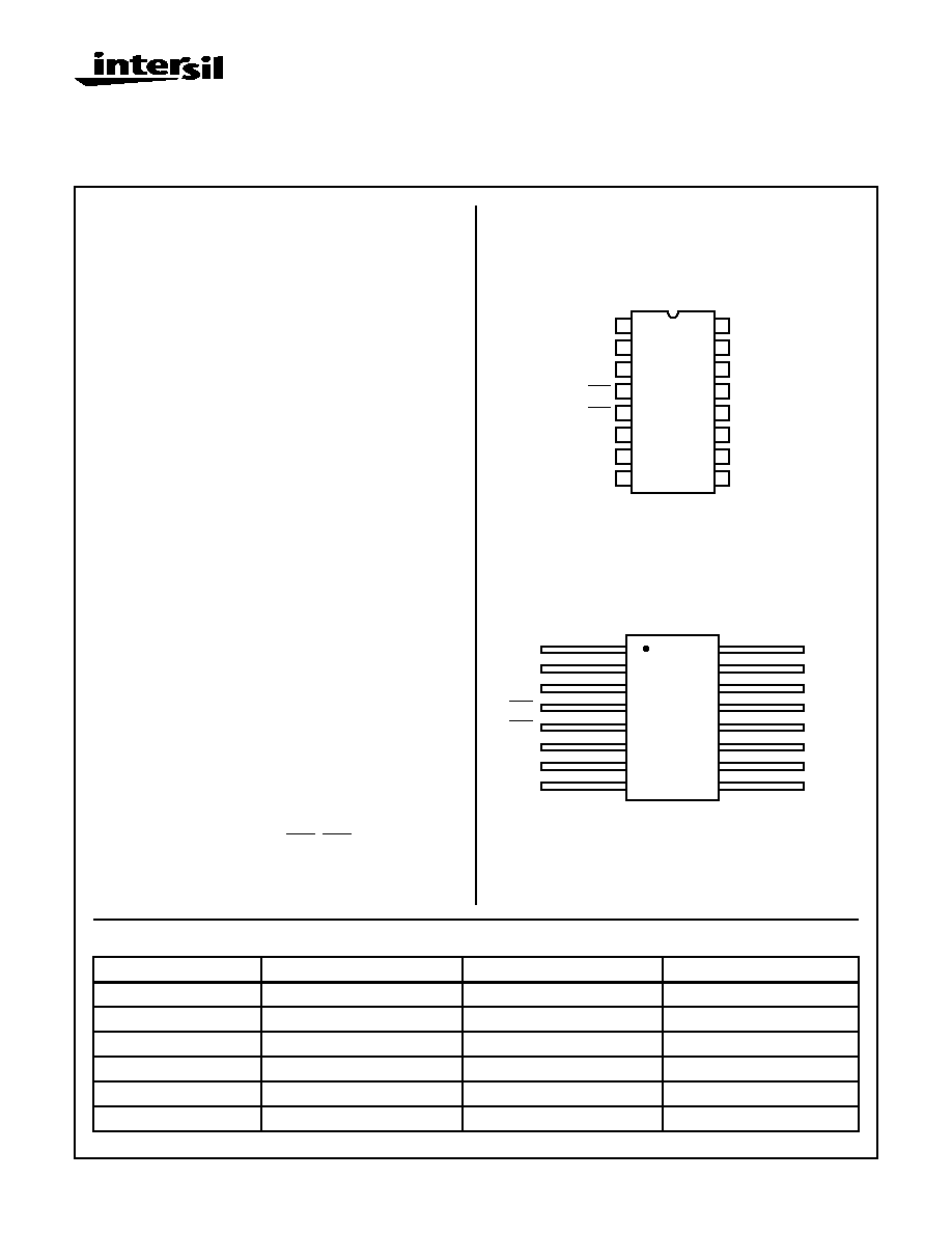
Pinouts
16 LEAD CERAMIC DUAL-IN-LINE
METAL SEAL PACKAGE (SBDIP)
MIL-STD-1835 CDIP2-T16
TOP VIEW
16 LEAD CERAMIC METAL SEAL
FLATPACK PACKAGE (FLATPACK)
MIL-STD-1835 CDFP4-F16
TOP VIEW
14
15
16
9
13
12
11
10
1
2
3
4
5
7
6
8
A
B
C
G2A
G2B
G1
GND
Y7
VDD
Y1
Y2
Y3
Y4
Y5
Y6
Y0
A
B
C
G2A
G2B
G1
Y7
GND
2
3
4
5
6
7
8
1
16
15
14
13
12
11
10
9
VDD
Y0
Y1
Y2
Y3
Y4
Y5
Y6
Features
∑ Devices QML Qualified in Accordance With
MIL-PRF-38535
∑ Detailed Electrical and Screening Requirements are
Contained in SMD# 5962-95825 and Intersil' QM Plan
∑ Radiation Hardened EPI-CMOS
- Total Dose 1 x 10
5
RAD (Si)
- Latch-Up Immune > 1 x 10
12
RAD (Si)/s
∑ Multiple Input Enable for Easy Expansion
∑ Single Power Supply +5V
∑ Outputs Active Low
∑ Low Standby Power (0.5mW Max at +5V)
∑ High Noise Immunity
∑ Equivalent to Sandia SA2995
∑ Bus Compatible with Intersil Rad-Hard 80C85RH
∑ Full Military Temperature Range -55
o
C to +125
o
C
Description
The Intersil HS-54C138RH is a radiation hardened 3- to 8-line
decoder fabricated using a radiation hardened EPI-CMOS pro-
cess. It features low power consumption, high noise immunity,
and high speed. Also featured are pin and function compatibility
with the 54LS138 industry standard part. The HS-54C138RH is
ideally suited for high speed memory chip select address
decoding. It is intended for use with the Intersil HS-80C85RH
radiation hardened microprocessor, but it can also be utilized as
a demultiplexer in any low power rad-hard application.
The HS-54C138RH contains a one of eight binary decoder.
A three bit binary input is used to select and activate each of
the eight outputs, provided the three chip enable inputs are
also present (see truth table).
The HS-54C138RH has an on-chip enable gate. The active
high (G1) and both active low (G2A, G2B) inputs are Anded
together to provide a single enable input to the device. The
use of both active high and active low inputs minimizes the
need for external gates when expanding a system.
February 1996
Spec Number
518053
File Number
3037.2
2
Specifications HS-54C138RH
Absolute Maximum Ratings
Reliability Information
Supply Voltage . . . . . . . . . . . . . . . . . . . . . . . . . . . . . . . . . . . . . +7.0V
I/O Voltage Applied. . . . . . . . . . . . . . . . . . GND -0.3V to VDD +0.3V
Storage Temperature Range . . . . . . . . . . . . . . . . . -65
o
C to +150
o
C
Junction Temperature . . . . . . . . . . . . . . . . . . . . . . . . . . . . . . +175
o
C
Lead Temperature (Soldering 10s) . . . . . . . . . . . . . . . . . . . . +300
o
C
ESD Classification . . . . . . . . . . . . . . . . . . . . . . . . . . . . . . . . Class 1
Thermal Resistance
JA
JC
SBDIP Package . . . . . . . . . . . . . . . . . . . .
73
o
C/W
24
o
C/W
Ceramic Flatpack Package . . . . . . . . . . .
114
o
C/W
29
o
C/W
Maximum Package Power Dissipation at +125
o
C Ambient
SBDIP Package . . . . . . . . . . . . . . . . . . . . . . . . . . . . . . . . . . 0.68W
Ceramic Flatpack Package . . . . . . . . . . . . . . . . . . . . . . . . . 0.44W
If device power exceeds package dissipation capability, provide heat
sinking or derate linearly at the following rate:
SBDIP Package . . . . . . . . . . . . . . . . . . . . . . . . . . . . . . 13.7mW/
o
C
Ceramic Flatpack Package . . . . . . . . . . . . . . . . . . . . . . 8.8mW/
o
C
CAUTION: Stresses above those listed in "Absolute Maximum Ratings" may cause permanent damage to the device. This is a stress only rating and operation
of the device at these or any other conditions above those indicated in the operational sections of this specification is not implied.
Operating Conditions
Operating Voltage Range . . . . . . . . . . . . . . . . . . . +4.75V to +5.25V
Operating Temperature Range . . . . . . . . . . . . . . . . -55
o
C to +125
o
C
Input Low Voltage . . . . . . . . . . . . . . . . . . . . . . . . . . . . . . . 0V to 1.0V
Input High Voltage . . . . . . . . . . . . . . . . . . . . . . . . . VDD-1.0V to VDD
TABLE 1. DC ELECTRICAL PERFORMANCE CHARACTERISTICS
PARAMETER
SYMBOL
CONDITIONS
GROUP A
SUBGROUPS
TEMPERATURE
LIMITS
UNITS
MIN
MAX
Input Leakage Current
High
IIH
VDD = 5.25V, VIN = 0V,
Pin Under Test = VDD
1, 2, 3
-55
o
C, +25
o
C,
+125
o
C
-
1
µ
A
Input Leakage Current
Low
IIL
VDD = 5.25V, VIN = 5.25V,
Pin Under Test = 0V
1, 2, 3
-55
o
C, +25
o
C
-1
-
µ
A
High Level Output
Voltage
VOH
VDD = 4.75V, IIN = -2mA
1, 2, 3
-55
o
C, +25
o
C,
+125
o
C
4.25
-
V
Low Level Output
Voltage
VOL
VDD = 5.25V, IIN = 2mA
1, 2, 3
-55
o
C, +25
o
C,
+125
o
C
0.5
-
V
Static Current
SIDD
VDD = 5.25V, VIN = GND
1, 2, 3
-55
o
C, +25
o
C,
+125
o
C
-
100
µ
A
Functional Tests
FT
VDD = 5.25V and 4.75V,
VIH = VDD - 1.0V, VIL = 1.0V
7, 8A, 8B
-55
o
C, +25
o
C,
+125
o
C
-
-
-
NOTE: All devices are guaranteed at worst case limits and conditions.
TABLE 2. AC ELECTRICAL PERFORMANCE CHARACTERISTICS
PARAMETER
SYMBOL
GROUP A SUB-
GROUPS
TEMPERATURE
LIMITS
UNITS
MIN
MAX
SELECT TO OUTPUT PROPAGATION DELAY TIME
Low to high level input, High to
low level output
TPHL11
9, 10, 11
-55
o
C, +25
o
C, +125
o
C
-
110
ns
Low to high level input, Low to
high level output
TPLH11
9, 10, 11
-55
o
C, +25
o
C, +125
o
C
-
65
ns
High to low level input, Low to
high level output
TPLH12
9, 10, 11
-55
o
C, +25
o
C, +125
o
C
-
75
ns
High to low level input, high to
low level output
TPHL12
9, 10, 11
-55
o
C, +25
o
C, +125
o
C
-
90
ns
ENABLE TO OUTPUT PROPAGATION DELAY TIME
Low to high level input, Low to
high level output
TPLH21
9, 10, 11
-55
o
C, +25
o
C, +125
o
C
-
70
ns
Spec Number
518053
3
HS-54C138RH
Low to high level input, High to
low level output
TPHL21
9, 10, 11
-55
o
C, +25
o
C, +125
o
C
-
105
ns
High to low level input, Low to
high level output
TPLH22
9, 10, 11
-55
o
C, +25
o
C, +125
o
C
-
70
ns
High to low level input, High to
low level output
TPHL22
9, 10, 11
-55
o
C, +25
o
C, +125
o
C
-
105
ns
NOTE: Output timings are measured with a capacitive load, CL = 100pF, VIH = 3.75V, and VIL = 1.0V.
TABLE 3. ELECTRICAL PERFORMANCE CHARACTERISTICS
PARAMETER
SYMBOL
CONDITIONS
TEMPERATURE
LIMITS
UNITS
MIN
MAX
Input Capacitance
CIN
VDD = Open, f = 1MHz, All Measurements
Referenced to Device Ground
+25
o
C
-
10
pF
Output Capacitance
COUT
VDD = Open, f = 1MHz, All Measurements
Referenced to Device Ground
+25
o
C
-
10
pF
NOTE: The parameters listed in Table 3 are controlled via design or process parameters and are not directly tested. These parameters are
characterized upon initial design release and upon design changes which would affect these characteristics.
TABLE 4. POST 100K RAD ELECTRICAL PERFORMANCE CHARACTERISTICS
NOTE:
The Post Irradiation test conditions and limits are the same as those listed in Table 1 and Table 2.
TABLE 5. BURN-IN DELTA PARAMETERS (+25
o
C; In Accordance With SMD)
TABLE 2. AC ELECTRICAL PERFORMANCE CHARACTERISTICS (Continued)
PARAMETER
SYMBOL
GROUP A SUB-
GROUPS
TEMPERATURE
LIMITS
UNITS
MIN
MAX
Spec Number
518053
4
HS-54C138RH
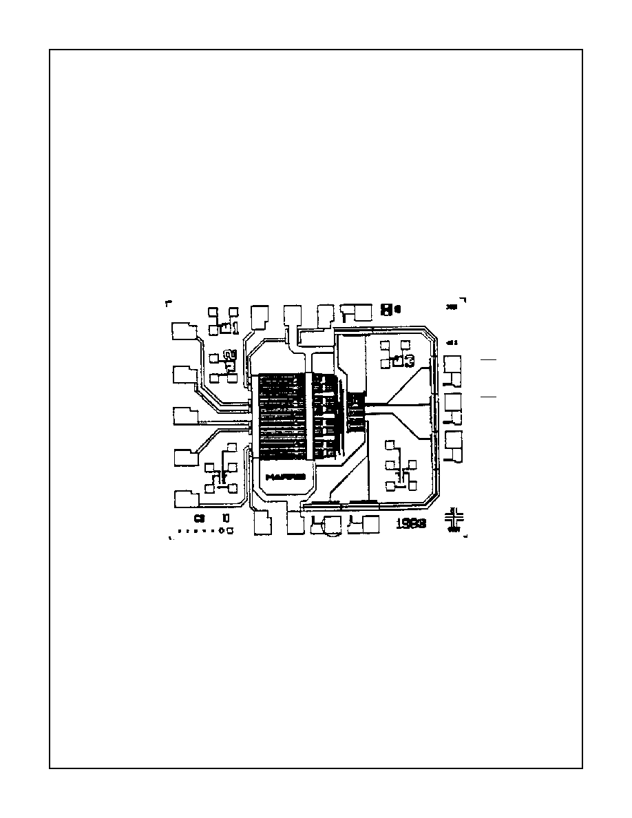
Metallization Topology
DIE DIMENSIONS:
76 mils x 63 mils x 14 mils
±
1 mil
METALLIZATION:
Type: AlSi
Thickness: 11k
≈
±
2k
≈
GLASSIVATION:
Type: SiO2
Thickness: 8k
≈
±
1k
≈
Metallization Mask Layout
HS-54C138RH
Y5 (10)
(5) G2B
(4) G2A
(3) C
Y4 (11)
Y3 (12)
Y2 (13)
Y1 (14)
(9) Y6
(8) GND
(7) Y7
(6) G1
Y0 (15)
VDD (16)
A (1)
B (2)
Spec Number
518053
5
HS-54C138RH
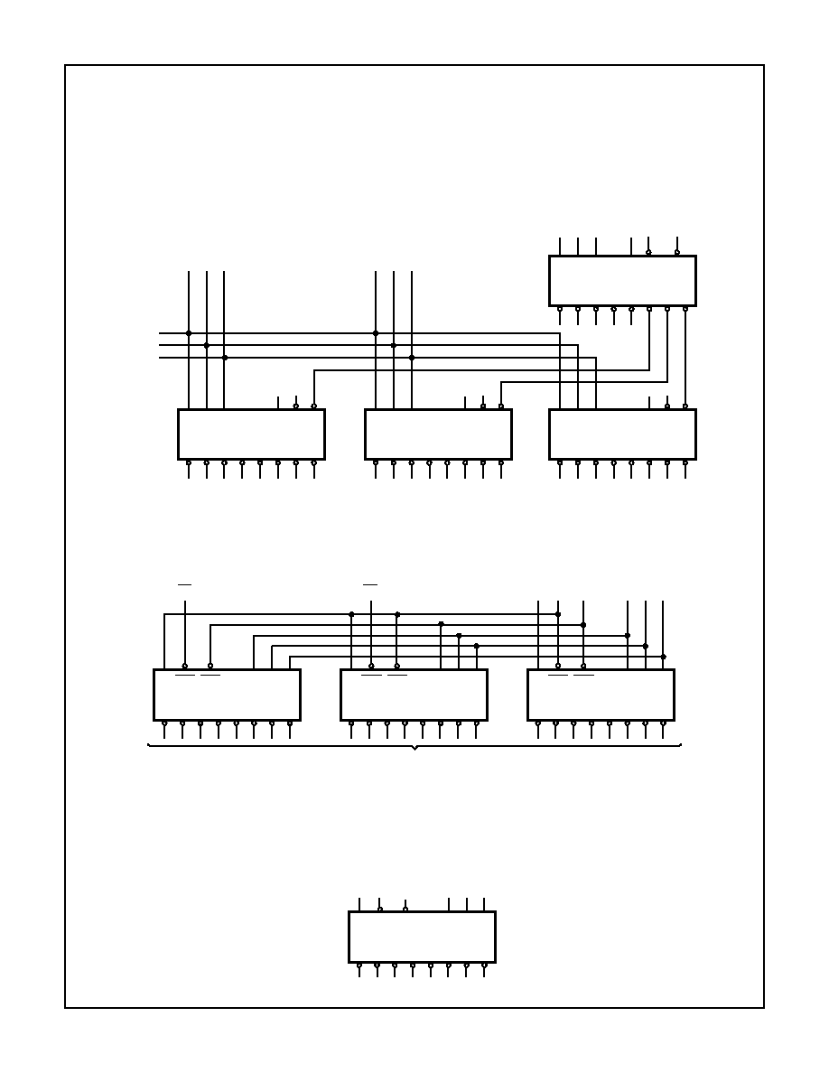
Typical applications include systems which require multiple
input/output ports and memories. When the HS-54C138RH
is enabled one of the eight outputs will go low. This output
can be used to select a particular device or a group of
devices. The HS-54C138RH can also be cascaded to
provide an enabling scheme for larger systems and allow
one decoder to control eight other decoders as in Figure 1.
Figure 2 shows a configuration that can be used to enable
multiple I/O ports or memory devices. Up to 24 memory
devices or I/O ports can be controlled using this circuit.
For demultiplexer operation, one of the three enable inputs is
used as the data input while the other two inputs are enable.
The transmitted data is distributed to the proper output as
determined by the 3-line select inputs. See Figure 3.
FIGURE 1
FIGURE 2
FIGURE 3
Y7 Y6 Y5 Y4 Y3 Y2 Y1 Y0
SELECT A
ENABLE
HS-54C138RH
Y7 Y6 Y5 Y4 Y3 Y2 Y1 Y0
HS-54C138RH
Y7 Y6 Y5 Y4 Y3 Y2 Y1 Y0
HS-54C138RH
Y7 Y6 Y5 Y4 Y3 Y2 Y1 Y0
HS-54C138RH
"0"
"1"
"0"
"1"
"0"
"1"
TO OTHER
DEVICES
SELECT B
ENABLE
ENABLE
ENABLE
Y7 Y6 Y5 Y4 Y3 Y2 Y1 Y0
G1 G2B G2A
C
B
A
Y7 Y6 Y5 Y4 Y3 Y2 Y1 Y0
G1 G2B G2A
C
B
A
Y7 Y6 Y5 Y4 Y3 Y2 Y1 Y0
G1 G2B G2A
C
B
A
EN
EN
EN A4
A3
A2 A1 A0
PORT NUMBERS OR CHIP SELECTS
Y7 Y6 Y5 Y4 Y3 Y2 Y1 Y0
G1 G2B G2A
C
B
A
DATA
INPUT
EN
EN
SELECT
Spec Number
518053