 | –≠–ª–µ–∫—Ç—Ä–æ–Ω–Ω—ã–π –∫–æ–º–ø–æ–Ω–µ–Ω—Ç: 631Z | –°–∫–∞—á–∞—Ç—å:  PDF PDF  ZIP ZIP |

1
Æ
FN7370.1
ISL97631
White LED Boost Regulator With
Integrated Schottky Diode
The ISL97631 represents a high efficiency, constant
frequency PWM regulator with integrated boost diode and
FET. Designed for use in white LED driving applications, the
ISL97631 features efficiencies up to 85%. It operates at
1.35MHz switching frequency and operates from an input
voltage of between 2.7V and 5.5V. The maximum output
voltage of 27V enables the ISL97631 to drive up to 6 LEDs in
series. It is also possible to use the ISL97631 to drive LEDs
in series/parallel combination for applications requiring up to
15 LEDs.
Available in the 6 Ld TSOT package, the ISL97631 offers
high efficiency, constant frequency operation. It is specified
for operation over the -40∞C to +85∞C ambient temperature
range.
Pinout
ISL97631
(6 LD TSOT)
TOP VIEW
Features
∑ Up to 6 LEDs in series
∑ 27V maximum output
∑ 2.7V to 5.5V input
∑ Up to 85% efficient
∑ 1.35MHz constant frequency
∑ Enable/PWM dimming control
∑ Pb-free plus anneal available (RoHS compliant)
Applications
∑ LED backlighting
∑ Cell phones
∑ PDAs
∑ Handheld games
∑ MP3 players
∑ GPS
∑ Other handheld devices
1
2
3
6
4
VOUT
GND
LX
VIN
ENAB
5 FB
Ordering Information
PART NUMBER
PART
MARKING
PCS.
TAPE &
REEL
PACKAGE
(TAPE AND REEL)
PKG. DWG. #
ISL97631IHTZ-T7 (See Note)
631Z
3,000
7"
6 Ld TSOT (Pb-free)
MDP0049
ISL97631IHTZ-T7A (See Note)
631Z
270
7"
6 Ld TSOT (Pb-free)
MDP0049
NOTE: Intersil Pb-free plus anneal products employ special Pb-free material sets; molding compounds/die attach materials and 100% matte tin plate
termination finish, which are RoHS compliant and compatible with both SnPb and Pb-free soldering operations. Intersil Pb-free products are MSL
classified at Pb-free peak reflow temperatures that meet or exceed the Pb-free requirements of IPC/JEDEC J STD-020.
Data Sheet
December 21, 2005
CAUTION: These devices are sensitive to electrostatic discharge; follow proper IC Handling Procedures.
1-888-INTERSIL or 1-888-468-3774
|
Intersil (and design) is a registered trademark of Intersil Americas Inc.
Copyright Intersil Americas Inc. 2005. All Rights Reserved
All other trademarks mentioned are the property of their respective owners.
2
FN7370.1
December 21, 2005
Absolute Maximum Ratings
(T
A
= 25∞C)
Thermal Information
Input Voltage (V
IN
) . . . . . . . . . . . . . . . . . . . . . . . . . . . . . -0.3V to +6V
LX, Vout Voltage . . . . . . . . . . . . . . . . . . . . . . . . . . . . . -0.3V to +27V
FB Voltage . . . . . . . . . . . . . . . . . . . . . . . . . . . . . . . . . . . -0.3V to +6V
ENAB Voltage . . . . . . . . . . . . . . . . . . . . . . . . . . . . . . . . -0.3V to +6V
Operating Temperature . . . . . . . . . . . . . . . . . . . . . . .-40∞C to +85∞C
Thermal Resistance (Typical, Note 1)
JA
(∞C/W)
6 Ld TSOT . . . . . . . . . . . . . . . . . . . . . . . . . . . . . . . .
190
Maximum Junction Temperature (Plastic Package . . . . . . . . . 150∞C
Maximum Storage Temperature Range . . . . . . . . . .-65∞C to +150∞C
Maximum Lead Temperature (Soldering, 10s). . . . . . . . . . . . +300∞C
(TSOT - Lead Tips Only)
CAUTION: Stresses above those listed in "Absolute Maximum Ratings" may cause permanent damage to the device. This is a stress only rating and operation of the
device at these or any other conditions above those indicated in the operational sections of this specification is not implied.
IMPORTANT NOTE: All parameters having Min/Max specifications are guaranteed over the specified temperature range. All parameters are based on pulsed tests,
therefore: T
J
= T
C
= T
A
NOTE:
1.
JA
is measured with the component mounted on a high effective thermal conductivity test board in free air. See Tech Brief TB379 for details.
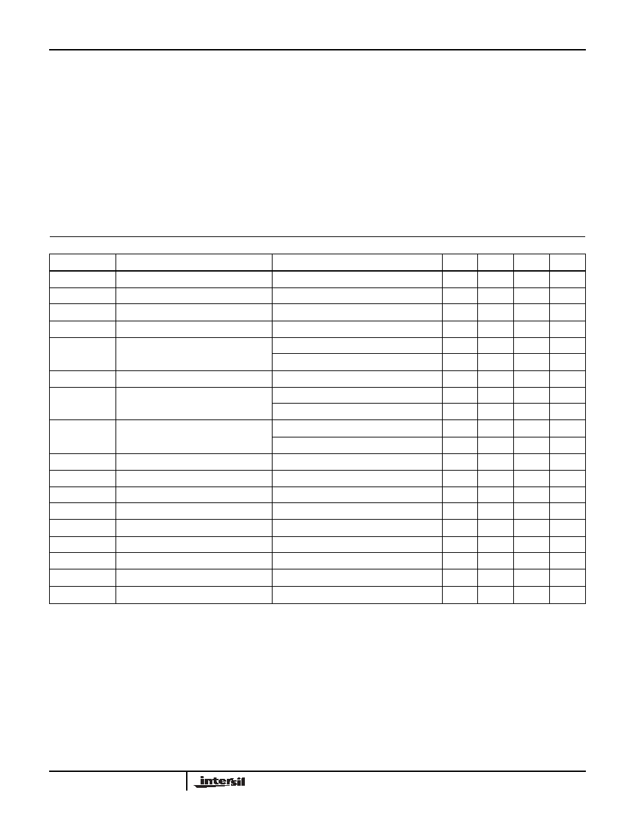
Electrical Specifications
V
IN
= 3V, V
ENAB
= 3V, T
A
= -40∞C to 85∞C unless otherwise specified.
PARAMETER
DESCRIPTION
CONDITION
MIN
TYP
MAX
UNIT
V
IN-MIN
Minimum Operating Voltage
V
OUT
= 16V, I
LED
= 20mA
2.7
V
V
IN-MAX
Maximum Operating Voltage
V
OUT
= 25V, I
LED
= 20mA
5.5
V
V
FB
Feedback Voltage
80
100
120
mV
I
FB
FB Pin Bias Current
100
nA
I
IN
Supply Current
ENAB = 3V, output not switching
0.6
1.0
mA
ENAB = 0V
1
µA
F
OSC
Switching Frequency
0.8
1.35
1.8
MHz
D
MAX
Maximum Duty Cycle
T
A
= 25∞C
85
90
%
82
90
%
I
LIM
Switch Current Limit
T
A
= 25∞C
280
350
mA
250
350
mA
r
DS(ON)
Switch On Resistance
I
LX
= 100mA
750
m
I
LEAK(LX)
Switch Leakage Current
V
LX
= 27V, Vout = 27V
0.01
1
µA
I
LEAK(VOUT)
Diode Leakage Current
V
OUT
= 27V
0.01
1
µA
V
DIODE
LX-V
OUT
Diode Forward Voltage
I
DIODE
= 100mA, T
A
= 25∞C
0.75
0.9
V
V
ENAB-HI
ENAB Voltage High
2.5
V
V
ENAB-LO
ENAB Voltage Low
0.6
V
I
ENAB
ENAB Pin Bias Current
1
µA
I
LED
/
V
IN
Line Regulation
V
IN
= 2.7V to 5V
0.2
%/V
Eff
Efficiency
I
LED
= 20mA, 3 LEDs
85
%
ISL97631

3
FN7370.1
December 21, 2005
Typical Application
FIGURE 1. TYPICAL APPLICATION CIRCUIT
FIGURE 2. EFFICIENCY vs LED CURRENT (V
IN
= 4V)
ISL97631
C1
L1
22µH
C2
0.22µF
R
SET
4.75
2.7V~5.5V
OFF/ON
LEDs
1µF
V
IN
LX
ENAB
FB
GND
V
IN
V
OUT
50
55
60
65
70
75
80
85
90
0
5
10
15
20
25
30
I
LED
(mA)
EFFICIENCY (%)
22µH, V
IN
= 4V
Typical Performance Curves
FIGURE 3. QUIESCENT CURRENT vs V
IN
(ENAB = hi)
FIGURE 4. LOAD REGULATION (V
IN
= 4V)
FIGURE 5. LINE REGULATION
FIGURE 6. SWITCHING FREQUENCY vs TEMPERATURE
0
100
200
300
400
500
600
700
0
2
4
Iq
(µ
A)
6
V
IN
(V)
18.228
18.230
18.232
18.234
18.236
18.238
18.240
18.242
18.244
0
5
10
15
20
V
OUT
(V)
I
O
(mA)
18.23
18.24
18.25
18.26
18.27
18.28
18.29
18.30
18.31
18.32
18.33
2.5
3.5
4.5
5.5
V
IN
(V)
I
O
(mA)
1.27
1.28
1.29
1.30
1.31
1.32
1.33
1.34
1.35
1.36
1.37
-60
-40
-20
0
20
40
60
80
100
TEMPERATURE (∞C)
FRE
Q
UENCY (MHz)
ISL97631
4
FN7370.1
December 21, 2005
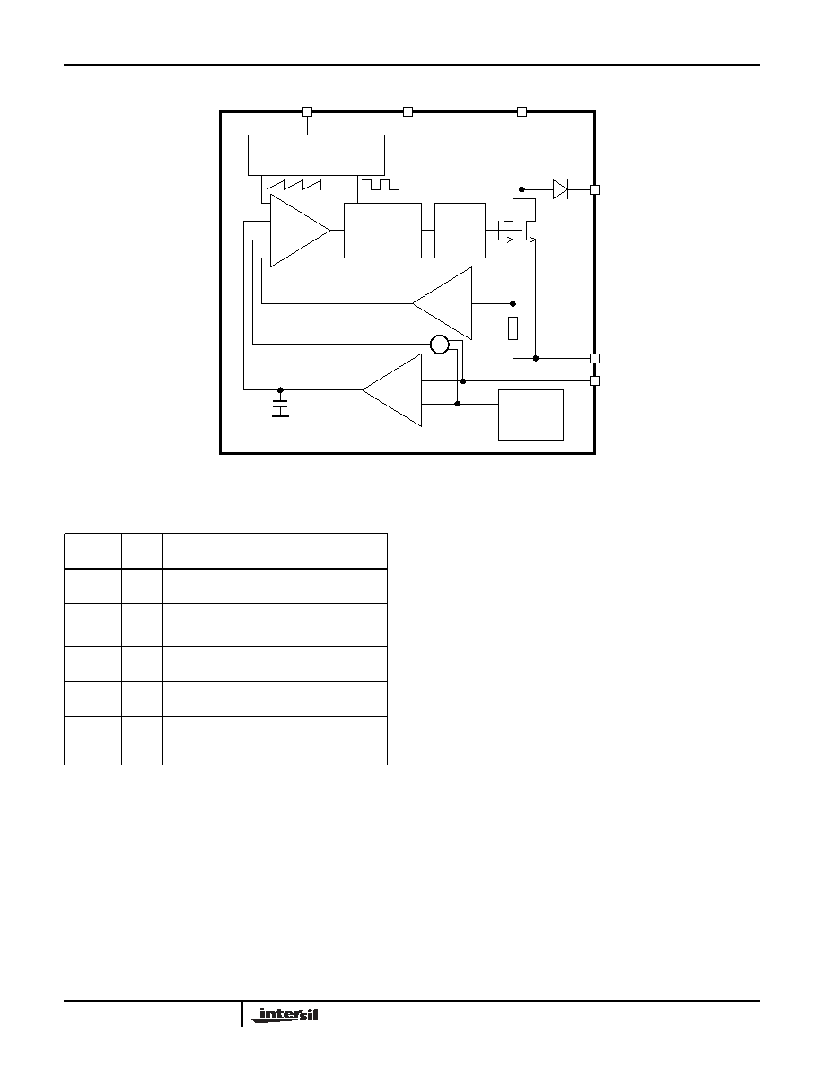
Block Diagram
Detailed Description
The ISL97631 uses a constant frequency, current mode
control scheme to provide excellent line and load
regulation. It can drive up to 6 LEDs in series or 15 LEDs in
parallel/series configuration, with efficiencies of up 85%.
The ISL97631 operates from an input voltage of 2.7V to
5.5V and can boost up to 27V.
Steady-State Operation
The ISL97631 operates with constant frequency PWM. The
switching frequency is around 1.35MHz. Depending on the
input voltage, inductance, number of LEDs and the LED
current, the converter operates in either continuous
conduction mode or discontinuous conduction mode. Both
are normal. The forward current of the LED is set using the
R
SET
resistor. In steady state mode, this current is given by
the equation:
Shut-Down
When taken low the ENAB pin places the ISL97631 into
power down mode. When in power down, the supply current
is reduced to less than 1µA.
Dimming Control
PWM DIMMING
The ENAB pin also doubles as a brightness control. There
are two different possible dimming control methods. The
first dimming method is controlled through the duty-cycle of
the ENAB input PWM waveform, which can operate at
frequencies up to 1kHz. For frequencies greater than 1kHz,
see Analog Dimming. The LEDs operate at either zero or
full current. This is the PWM dimming control method. The
relationship between the average LED current and the
duty-cycle (D) of the ENAB pin's waveform is as follows:
FIGURE 7. ISL97631 BLOCK DIAGRAM
FET
Driver
PWM Logic
Controller
Current
Sense
GM
Amplifier
1.2MHz Oscillator and Ramp
Generator
Bandgap
Reference
Generator
95mV
GM Amp
Compensation
PWM
Comparator
Vin
Enable
LX
GND
FB
ISL97631
Vout
-
FET
Driver
PWM Logic
Controller
Current
Sense
GM
Amplifier
1.2MHz Oscillator and Ramp
Generator
Bandgap
Reference
Generator
95mV
GM Amp
Compensation
PWM
Comparator
Vin
Enable
LX
GND
FB
ISL97631
Vout
-
1.35MHz
Pin Descriptions
PIN
NUMBER
PIN
NAME
DESCRIPTION
1
VOUT Output Pin. Connect to the anode of the top
LED and the output filter capacitor .
2
GND
Ground Pin. Connect to local ground.
3
LX
Switching Pin. Connect to inductor.
4
ENAB Enable Pin. Connect to enable signal to turn-on
or off the device.
5
FB
Feedback Pin. Connect to the cathode of
bottom LED and the sense resistor.
6
VIN
Input Supply Pin. Connect to the input supply
voltage, the inductor and the input supply
decoupling capacitor.
I
LED
V
FB
R
SET
---------------
=
(EQ. 1)
average I
LED
V
FB
R
SET
--------------- D
=
(EQ. 2)
ISL97631

5
FN7370.1
December 21, 2005
The magnitude of the PWM signal should be higher than the
minimum ENAB voltage high. The bench PWM dimming test
results are shown in Figure 8. In the test, two PWM
frequencies 400Hz and 1kHz are chosen to compare the
linear dimming range. It is clear that there is a wider linear
dimming range for the lower PWM frequency than for the
higher one, due to the self discharge of the output capacitor
through the LEDs during the low ENAB periods. To achieve
a better linearity with high frequencies an NMOS FET can be
placed between the FB pin and the LED stack, with its gate
driven by the same signal as ENAB. This acts to prevent self
discharge of the output capacitor during the off periods. In
the PWM dimming test, the output capacitor is 0.22µF.
ANALOG DIMMING
The second dimming method applies a variable DC voltage
(V
Dim
) at FB pin (see Figure 9) to adjust the LED current. As
the DC dimming signal voltage increases above V
FB
, the
voltages drop on R
1
and R
2
increase and the voltage drop
on R
SET
decreases. Thus, the LED current decreases.
The DC dimming signal voltage can be a variable DC voltage
or a DC voltage generated by filtering a high frequency PWM
control signal.
As brightness is directly proportional to LED currents, V
Dim
may be calculated for any desired "relative brightness" (F)
using Equation 4.
Where F = I
LED
(dimmed)/I
LED
(undimmed).
These equations are valid for values of R1 and R2 such that
both R1>>RSET and R2>>RSET.
The analog dimming circuit can be tailored to a desired
relative brightness for different V
Dim
ranges using
Equation 5.
Where V
Dim_max
is the maximum V
Dim
voltage and F
min
is
the minimum relative brightness (i.e., the brightness with
V
Dim_max
applied).
i.e., V
Dim_max
= 5V, F
min
= 10% (i.e., 0.1), R
2
= 189k
i.e., V
Dim_max
= 1V, F
min
= 10% (i.e., 0.1), R
2
= 35k
Open-Voltage Protection
In some applications, it is possible that the output is
opened, e.g. when the LEDs are disconnected from the
circuit or the LEDs fail. In this case the feedback voltage
will be zero. The ISL97631 will then switch to a high duty
cycle resulting in a high output voltage, which may cause
the LX pin voltage to exceed its maximum 27V rating. To
implement overvoltage protection, a zener diode Dz and a
resistor R
1
can be used at the output and FB pin to limit the
voltage on the LX pin as shown in Figure 10. It is clear that
as the zener is turned on, due to the overvoltage, the zener
diode's current will set up a voltage on R
1
and R
SET
and this
voltage is applied on FB pin as the feedback node. This
feedback will prevent the output from reaching the
overvoltage condition. In the overvoltage protection circuit
design, the zener voltage should be larger than the
maximum forward voltage of the LED string.
FIGURE 8. PWM DIMMING LINEAR RANGE (FOR 400Hz AND
1kHz PWM FREQUENCIES CONDITION,
C
OUT
= 0.22µF)
0
2
4
6
8
10
12
14
16
18
20
0
20
40
60
80
100
DUTY-CYCLE (%)
I
O
(mA)
400Hz
1kHz
I
LED
V
FB
R
1
R
2
+
(
) V
Dim
R
1
≠
R
2
R
SET
--------------------------------------------------------------------------
=
(EQ. 3)
V
Dim
R
2
R
1
------- V
FB
1
R
1
R
2
------- F
≠
+
=
(EQ. 4)
FIGURE 9. ANALOG DIMMING CONTROL APPLICATION
CIRCUIT
ISL97631
C1
V
IN
LX
ENAB
FB
GND
L1
22µH
C2
0.22µF
R
SET
4.75
OFF/ON
LEDs
1µF
LX
V
IN
2.7V~5.5V
R1
R2
V
Dim
V
OUT
3.3k
R
2
V
Dim_max
V
FB
≠
(
) R
1
∑
[
]
V
FB
1 F
min
≠
(
)
∑
[
]
-------------------------------------------------------------------
=
(EQ. 5)
ISL97631